EP2437303A1 - Transistor avec plaque de champ. - Google Patents
Transistor avec plaque de champ. Download PDFInfo
- Publication number
- EP2437303A1 EP2437303A1 EP11183655A EP11183655A EP2437303A1 EP 2437303 A1 EP2437303 A1 EP 2437303A1 EP 11183655 A EP11183655 A EP 11183655A EP 11183655 A EP11183655 A EP 11183655A EP 2437303 A1 EP2437303 A1 EP 2437303A1
- Authority
- EP
- European Patent Office
- Prior art keywords
- gate
- field plate
- transistor
- spacer layer
- layer
- Prior art date
- Legal status (The legal status is an assumption and is not a legal conclusion. Google has not performed a legal analysis and makes no representation as to the accuracy of the status listed.)
- Ceased
Links
- 125000006850 spacer group Chemical group 0.000 claims abstract description 136
- 239000000758 substrate Substances 0.000 claims abstract description 34
- 239000004065 semiconductor Substances 0.000 claims abstract description 16
- 230000004888 barrier function Effects 0.000 claims description 45
- 230000006911 nucleation Effects 0.000 claims description 19
- 238000010899 nucleation Methods 0.000 claims description 19
- 229910002601 GaN Inorganic materials 0.000 claims description 17
- HBMJWWWQQXIZIP-UHFFFAOYSA-N silicon carbide Chemical group [Si+]#[C-] HBMJWWWQQXIZIP-UHFFFAOYSA-N 0.000 claims description 16
- 229910010271 silicon carbide Inorganic materials 0.000 claims description 16
- 238000002161 passivation Methods 0.000 claims description 12
- 229910052751 metal Inorganic materials 0.000 claims description 11
- 239000002184 metal Substances 0.000 claims description 11
- 230000005684 electric field Effects 0.000 claims description 7
- 230000005669 field effect Effects 0.000 claims description 6
- 150000004767 nitrides Chemical class 0.000 claims description 5
- 230000005533 two-dimensional electron gas Effects 0.000 claims description 4
- 230000009467 reduction Effects 0.000 claims description 3
- JMASRVWKEDWRBT-UHFFFAOYSA-N Gallium nitride Chemical compound [Ga]#N JMASRVWKEDWRBT-UHFFFAOYSA-N 0.000 claims description 2
- 239000000463 material Substances 0.000 description 34
- 229910002704 AlGaN Inorganic materials 0.000 description 15
- 239000003989 dielectric material Substances 0.000 description 12
- 238000000034 method Methods 0.000 description 9
- 230000015572 biosynthetic process Effects 0.000 description 8
- JBRZTFJDHDCESZ-UHFFFAOYSA-N AsGa Chemical compound [As]#[Ga] JBRZTFJDHDCESZ-UHFFFAOYSA-N 0.000 description 6
- 229910052581 Si3N4 Inorganic materials 0.000 description 6
- 230000008901 benefit Effects 0.000 description 6
- 238000000151 deposition Methods 0.000 description 6
- HQVNEWCFYHHQES-UHFFFAOYSA-N silicon nitride Chemical compound N12[Si]34N5[Si]62N3[Si]51N64 HQVNEWCFYHHQES-UHFFFAOYSA-N 0.000 description 6
- 229910001218 Gallium arsenide Inorganic materials 0.000 description 5
- 239000004020 conductor Substances 0.000 description 5
- 230000008021 deposition Effects 0.000 description 5
- PXHVJJICTQNCMI-UHFFFAOYSA-N Nickel Chemical compound [Ni] PXHVJJICTQNCMI-UHFFFAOYSA-N 0.000 description 4
- 230000015556 catabolic process Effects 0.000 description 3
- 230000008878 coupling Effects 0.000 description 3
- 238000010168 coupling process Methods 0.000 description 3
- 238000005859 coupling reaction Methods 0.000 description 3
- 230000000694 effects Effects 0.000 description 3
- 230000006872 improvement Effects 0.000 description 3
- 229910016920 AlzGa1−z Inorganic materials 0.000 description 2
- KDLHZDBZIXYQEI-UHFFFAOYSA-N Palladium Chemical compound [Pd] KDLHZDBZIXYQEI-UHFFFAOYSA-N 0.000 description 2
- XUIMIQQOPSSXEZ-UHFFFAOYSA-N Silicon Chemical compound [Si] XUIMIQQOPSSXEZ-UHFFFAOYSA-N 0.000 description 2
- 229910001069 Ti alloy Inorganic materials 0.000 description 2
- XLOMVQKBTHCTTD-UHFFFAOYSA-N Zinc monoxide Chemical compound [Zn]=O XLOMVQKBTHCTTD-UHFFFAOYSA-N 0.000 description 2
- 229910052782 aluminium Inorganic materials 0.000 description 2
- PCHJSUWPFVWCPO-UHFFFAOYSA-N gold Chemical compound [Au] PCHJSUWPFVWCPO-UHFFFAOYSA-N 0.000 description 2
- 229910052737 gold Inorganic materials 0.000 description 2
- 239000010931 gold Substances 0.000 description 2
- 238000004519 manufacturing process Methods 0.000 description 2
- 229910052759 nickel Inorganic materials 0.000 description 2
- BASFCYQUMIYNBI-UHFFFAOYSA-N platinum Chemical compound [Pt] BASFCYQUMIYNBI-UHFFFAOYSA-N 0.000 description 2
- 229910052594 sapphire Inorganic materials 0.000 description 2
- 239000010980 sapphire Substances 0.000 description 2
- 229910052710 silicon Inorganic materials 0.000 description 2
- 239000010703 silicon Substances 0.000 description 2
- 238000012360 testing method Methods 0.000 description 2
- ZXEYZECDXFPJRJ-UHFFFAOYSA-N $l^{3}-silane;platinum Chemical compound [SiH3].[Pt] ZXEYZECDXFPJRJ-UHFFFAOYSA-N 0.000 description 1
- VYZAMTAEIAYCRO-UHFFFAOYSA-N Chromium Chemical compound [Cr] VYZAMTAEIAYCRO-UHFFFAOYSA-N 0.000 description 1
- RTAQQCXQSZGOHL-UHFFFAOYSA-N Titanium Chemical compound [Ti] RTAQQCXQSZGOHL-UHFFFAOYSA-N 0.000 description 1
- 229910001080 W alloy Inorganic materials 0.000 description 1
- 229910045601 alloy Inorganic materials 0.000 description 1
- 239000000956 alloy Substances 0.000 description 1
- XAGFODPZIPBFFR-UHFFFAOYSA-N aluminium Chemical compound [Al] XAGFODPZIPBFFR-UHFFFAOYSA-N 0.000 description 1
- 230000003321 amplification Effects 0.000 description 1
- 230000001413 cellular effect Effects 0.000 description 1
- 238000005229 chemical vapour deposition Methods 0.000 description 1
- 229910052804 chromium Inorganic materials 0.000 description 1
- 239000011651 chromium Substances 0.000 description 1
- PMHQVHHXPFUNSP-UHFFFAOYSA-M copper(1+);methylsulfanylmethane;bromide Chemical compound Br[Cu].CSC PMHQVHHXPFUNSP-UHFFFAOYSA-M 0.000 description 1
- 239000013078 crystal Substances 0.000 description 1
- 238000013461 design Methods 0.000 description 1
- 238000011161 development Methods 0.000 description 1
- 238000004870 electrical engineering Methods 0.000 description 1
- 238000010893 electron trap Methods 0.000 description 1
- 238000000407 epitaxy Methods 0.000 description 1
- 238000005530 etching Methods 0.000 description 1
- 229910052733 gallium Inorganic materials 0.000 description 1
- 238000013101 initial test Methods 0.000 description 1
- 150000002500 ions Chemical class 0.000 description 1
- 229910052741 iridium Inorganic materials 0.000 description 1
- GKOZUEZYRPOHIO-UHFFFAOYSA-N iridium atom Chemical compound [Ir] GKOZUEZYRPOHIO-UHFFFAOYSA-N 0.000 description 1
- 238000002955 isolation Methods 0.000 description 1
- 238000001465 metallisation Methods 0.000 description 1
- 238000001451 molecular beam epitaxy Methods 0.000 description 1
- 238000003199 nucleic acid amplification method Methods 0.000 description 1
- 229910052763 palladium Inorganic materials 0.000 description 1
- 238000005424 photoluminescence Methods 0.000 description 1
- 229910052697 platinum Inorganic materials 0.000 description 1
- 229910021339 platinum silicide Inorganic materials 0.000 description 1
- 230000000284 resting effect Effects 0.000 description 1
- 239000007787 solid Substances 0.000 description 1
- -1 spinet Chemical compound 0.000 description 1
- 230000007480 spreading Effects 0.000 description 1
- 238000003892 spreading Methods 0.000 description 1
- 229910052719 titanium Inorganic materials 0.000 description 1
- 239000010936 titanium Substances 0.000 description 1
- WFKWXMTUELFFGS-UHFFFAOYSA-N tungsten Chemical compound [W] WFKWXMTUELFFGS-UHFFFAOYSA-N 0.000 description 1
- 239000010937 tungsten Substances 0.000 description 1
Images

Classifications
-
- H—ELECTRICITY
- H01—ELECTRIC ELEMENTS
- H01L—SEMICONDUCTOR DEVICES NOT COVERED BY CLASS H10
- H01L29/00—Semiconductor devices specially adapted for rectifying, amplifying, oscillating or switching and having potential barriers; Capacitors or resistors having potential barriers, e.g. a PN-junction depletion layer or carrier concentration layer; Details of semiconductor bodies or of electrodes thereof ; Multistep manufacturing processes therefor
- H01L29/66—Types of semiconductor device ; Multistep manufacturing processes therefor
- H01L29/68—Types of semiconductor device ; Multistep manufacturing processes therefor controllable by only the electric current supplied, or only the electric potential applied, to an electrode which does not carry the current to be rectified, amplified or switched
- H01L29/76—Unipolar devices, e.g. field effect transistors
- H01L29/772—Field effect transistors
- H01L29/778—Field effect transistors with two-dimensional charge carrier gas channel, e.g. HEMT ; with two-dimensional charge-carrier layer formed at a heterojunction interface
-
- H—ELECTRICITY
- H01—ELECTRIC ELEMENTS
- H01L—SEMICONDUCTOR DEVICES NOT COVERED BY CLASS H10
- H01L29/00—Semiconductor devices specially adapted for rectifying, amplifying, oscillating or switching and having potential barriers; Capacitors or resistors having potential barriers, e.g. a PN-junction depletion layer or carrier concentration layer; Details of semiconductor bodies or of electrodes thereof ; Multistep manufacturing processes therefor
- H01L29/40—Electrodes ; Multistep manufacturing processes therefor
- H01L29/402—Field plates
-
- H—ELECTRICITY
- H01—ELECTRIC ELEMENTS
- H01L—SEMICONDUCTOR DEVICES NOT COVERED BY CLASS H10
- H01L29/00—Semiconductor devices specially adapted for rectifying, amplifying, oscillating or switching and having potential barriers; Capacitors or resistors having potential barriers, e.g. a PN-junction depletion layer or carrier concentration layer; Details of semiconductor bodies or of electrodes thereof ; Multistep manufacturing processes therefor
- H01L29/40—Electrodes ; Multistep manufacturing processes therefor
- H01L29/41—Electrodes ; Multistep manufacturing processes therefor characterised by their shape, relative sizes or dispositions
- H01L29/423—Electrodes ; Multistep manufacturing processes therefor characterised by their shape, relative sizes or dispositions not carrying the current to be rectified, amplified or switched
- H01L29/42312—Gate electrodes for field effect devices
- H01L29/42316—Gate electrodes for field effect devices for field-effect transistors
-
- H—ELECTRICITY
- H01—ELECTRIC ELEMENTS
- H01L—SEMICONDUCTOR DEVICES NOT COVERED BY CLASS H10
- H01L29/00—Semiconductor devices specially adapted for rectifying, amplifying, oscillating or switching and having potential barriers; Capacitors or resistors having potential barriers, e.g. a PN-junction depletion layer or carrier concentration layer; Details of semiconductor bodies or of electrodes thereof ; Multistep manufacturing processes therefor
- H01L29/66—Types of semiconductor device ; Multistep manufacturing processes therefor
- H01L29/68—Types of semiconductor device ; Multistep manufacturing processes therefor controllable by only the electric current supplied, or only the electric potential applied, to an electrode which does not carry the current to be rectified, amplified or switched
- H01L29/76—Unipolar devices, e.g. field effect transistors
- H01L29/762—Charge transfer devices
- H01L29/765—Charge-coupled devices
- H01L29/768—Charge-coupled devices with field effect produced by an insulated gate
-
- H—ELECTRICITY
- H01—ELECTRIC ELEMENTS
- H01L—SEMICONDUCTOR DEVICES NOT COVERED BY CLASS H10
- H01L29/00—Semiconductor devices specially adapted for rectifying, amplifying, oscillating or switching and having potential barriers; Capacitors or resistors having potential barriers, e.g. a PN-junction depletion layer or carrier concentration layer; Details of semiconductor bodies or of electrodes thereof ; Multistep manufacturing processes therefor
- H01L29/66—Types of semiconductor device ; Multistep manufacturing processes therefor
- H01L29/68—Types of semiconductor device ; Multistep manufacturing processes therefor controllable by only the electric current supplied, or only the electric potential applied, to an electrode which does not carry the current to be rectified, amplified or switched
- H01L29/76—Unipolar devices, e.g. field effect transistors
- H01L29/772—Field effect transistors
- H01L29/778—Field effect transistors with two-dimensional charge carrier gas channel, e.g. HEMT ; with two-dimensional charge-carrier layer formed at a heterojunction interface
- H01L29/7786—Field effect transistors with two-dimensional charge carrier gas channel, e.g. HEMT ; with two-dimensional charge-carrier layer formed at a heterojunction interface with direct single heterostructure, i.e. with wide bandgap layer formed on top of active layer, e.g. direct single heterostructure MIS-like HEMT
- H01L29/7787—Field effect transistors with two-dimensional charge carrier gas channel, e.g. HEMT ; with two-dimensional charge-carrier layer formed at a heterojunction interface with direct single heterostructure, i.e. with wide bandgap layer formed on top of active layer, e.g. direct single heterostructure MIS-like HEMT with wide bandgap charge-carrier supplying layer, e.g. direct single heterostructure MODFET
-
- H—ELECTRICITY
- H01—ELECTRIC ELEMENTS
- H01L—SEMICONDUCTOR DEVICES NOT COVERED BY CLASS H10
- H01L29/00—Semiconductor devices specially adapted for rectifying, amplifying, oscillating or switching and having potential barriers; Capacitors or resistors having potential barriers, e.g. a PN-junction depletion layer or carrier concentration layer; Details of semiconductor bodies or of electrodes thereof ; Multistep manufacturing processes therefor
- H01L29/66—Types of semiconductor device ; Multistep manufacturing processes therefor
- H01L29/68—Types of semiconductor device ; Multistep manufacturing processes therefor controllable by only the electric current supplied, or only the electric potential applied, to an electrode which does not carry the current to be rectified, amplified or switched
- H01L29/76—Unipolar devices, e.g. field effect transistors
- H01L29/772—Field effect transistors
- H01L29/80—Field effect transistors with field effect produced by a PN or other rectifying junction gate, i.e. potential-jump barrier
- H01L29/812—Field effect transistors with field effect produced by a PN or other rectifying junction gate, i.e. potential-jump barrier with a Schottky gate
-
- H—ELECTRICITY
- H01—ELECTRIC ELEMENTS
- H01L—SEMICONDUCTOR DEVICES NOT COVERED BY CLASS H10
- H01L29/00—Semiconductor devices specially adapted for rectifying, amplifying, oscillating or switching and having potential barriers; Capacitors or resistors having potential barriers, e.g. a PN-junction depletion layer or carrier concentration layer; Details of semiconductor bodies or of electrodes thereof ; Multistep manufacturing processes therefor
- H01L29/02—Semiconductor bodies ; Multistep manufacturing processes therefor
- H01L29/12—Semiconductor bodies ; Multistep manufacturing processes therefor characterised by the materials of which they are formed
- H01L29/16—Semiconductor bodies ; Multistep manufacturing processes therefor characterised by the materials of which they are formed including, apart from doping materials or other impurities, only elements of Group IV of the Periodic Table
- H01L29/1608—Silicon carbide
-
- H—ELECTRICITY
- H01—ELECTRIC ELEMENTS
- H01L—SEMICONDUCTOR DEVICES NOT COVERED BY CLASS H10
- H01L29/00—Semiconductor devices specially adapted for rectifying, amplifying, oscillating or switching and having potential barriers; Capacitors or resistors having potential barriers, e.g. a PN-junction depletion layer or carrier concentration layer; Details of semiconductor bodies or of electrodes thereof ; Multistep manufacturing processes therefor
- H01L29/02—Semiconductor bodies ; Multistep manufacturing processes therefor
- H01L29/12—Semiconductor bodies ; Multistep manufacturing processes therefor characterised by the materials of which they are formed
- H01L29/20—Semiconductor bodies ; Multistep manufacturing processes therefor characterised by the materials of which they are formed including, apart from doping materials or other impurities, only AIIIBV compounds
- H01L29/2003—Nitride compounds
Definitions
- the present invention relates to transistors and particularly to transistors utilizing field plates.
- High electron mobility transistors are a common type of solid state transistor that are regularly fabricated from semiconductor materials such as Silicon (Si) or Gallium Arsenide (GaAs).
- Si Silicon
- GaAs Gallium Arsenide
- One disadvantage of Si is that it has low electron mobility (600 - 1450 cm 2 /V-s), which produces a high source resistance. This resistance can degrade the Si based HEMT's high performance gain.
- GaAs based HEMTs have become the standard for signal amplification in civil and military radar, handset cellular, and satellite communications.
- GaAs has a higher electron mobility (approximately 6000 cm 2 /V-s) and a lower source resistance than Si, which allows GaAs based devices to function at higher frequencies.
- GaAs has a relatively small bandgap (1.42 eV at room temperature) and relatively small breakdown voltage, which prevents GaAs based HEMTs from providing high power at high frequencies.
- AlGaN/GaN has large bandgaps, as well as high peak and saturation electron velocity values [ B. Belmont, K. Kim and M. Shur, J.Appl.Phys. 74, 1818 (1993 )].
- AlGaN/GaN HEMTs can also have two dimensional electron gas (2DEG) sheet densities in excess of 10 13/ cm 2 and relatively high electron mobility (up to 2019 cm 2 /Vs) [ R. Gaska, J.W. Yang, A. Osinsky, Q. Chen, M.A.
- 2DEG two dimensional electron gas
- AlGaN/GaN HEMTs to provide very high voltage and high power operation at RF, microwave and millimeter wave frequencies.
- AlGaN/GaN HEMTs have been grown on sapphire substrates and have shown a power density of 4.6 W/mm and a total power of 7.6 W [ Y.F. Wu et al., IEICE Trans.Electron., E-82-C, 1895 (1999 )]. More recently, AlGaN/GaN HEMTs grown on SiC have shown a power density of 9.8 W/mm at 8 GHz [ Y.F. Wu, D. Kapolnek, J.P. Ibbetson, P. Parikh, B.P. Keller and U.K.
- U.S. Patent number 5,192,987 to Khan et al. discloses GaN/AlGaN based HEMTs grown on a buffer and a substrate.
- Other AlGaN/GaN HEMTs and field effect transistors (FETs) have been described by Gaska et al., "High-Temperature Performance of AlGaN/GaN HFET's on SiC substrates," IEEE Electron Device Letters, Vol. 18, No 10, October 1997, Page 492 ; and Ping et al., "DC and Microwave Performance of High Current AlGaN Heterostructure Field Effect Transistors Grown on P-type SiC Substrates," IEEE Electron Devices Letters, Vol. 19, No. 2, February 1998, Page 54 .
- Electron trapping and the resulting difference between DC and RF characteristics have been a limiting factor in the performance of GaN based transistors, such as AlGaN/GaN HEMTs.
- Silicon Nitride (SiN) passivation has been successfully employed to alleviate this trapping problem, which has resulted in high performance devices with power densities over 10W/mm at 10 Ghz.
- U.S. Patent No. 6,586,781 discloses methods and structures for reducing the trapping effect in GaN-based transistors. However, due to the high electric fields existing in these structures, charge trapping can still be an issue.
- One transistor according to the present invention comprises a plurality of active semiconductor layers formed on a substrate.
- a source contact is formed in electrical contact with the plurality of active layers, and a drain contact is also formed in electrical contact with the plurality of active layers with space between the source and drain contacts on the topmost of the plurality of active layers.
- a gate is formed in electrical contact with the topmost of the plurality of active layers, between the source and drain contacts.
- a spacer layer of epitaxial material is formed on the surface of the topmost of the plurality of active layers, between the gate and the drain contact, wherein the gate is not covered by the spacer layer.
- a field plate is formed on the spacer layer integral to the gate.
- Another embodiment of a transistor according to the present invention comprises a plurality of active semiconductor layers formed on a substrate.
- a source contact is formed in electrical contact with the plurality of active layers.
- a drain contact is also formed in electrical contact with the plurality of active layers with space between the source and drain contacts on the topmost of the plurality of active layers.
- a gate is formed in electrical contact with the topmost of the plurality of active layers, between the source and drain contacts.
- a spacer layer is formed on the surface of the topmost of the plurality of active layers, between the gate and the drain contact, and covering the gate contact.
- a field plate is formed on the spacer layer and is electrically connected to the gate.
- Another embodiment of a transistor according to the present invention' comprises a plurality of active semiconductor layers formed on a substrate.
- Source and drain contacts are formed in electrical contact with the plurality of active layers.
- a gate is formed in electrical contact with the topmost of the plurality of active layers, between the source and drain contacts.
- a first spacer layer formed on the surface of the topmost of the plurality of active layers, between the gate and the drain contact, wherein the gate is not covered by the spacer layer.
- a first field plate formed on the spacer layer integral to the gate and extending toward the drain contact on the spacer layer.
- a second spacer layer covering the field plate and the surface of the spacer layer between the field plate and drain contact, and further comprising a second field plate on the second spacer layer and extending from the edge of the gate toward the drain contact.
- Wide bandgap transistor structures generally include an active region, with metal source and drain contacts formed in electrical contact with the active region, and a gate contact formed between the source and drain contacts for modulating electric fields within the active region.
- a spacer layer is formed above the active region.
- the spacer layer can comprise a dielectric layer, a layer of epitaxial material such as an undoped or depleted wide bandgap epitaxial material, or a combination thereof.
- a conductive field plate is formed above the spacer layer and extends a distance L f from the edge of the gate contact toward the drain contact.
- the field plate can be electrically connected to the gate contact.
- This field plate arrangement can reduce the peak electric field in the device, resulting in increased breakdown voltage and reduced trapping. The reduction of the electric field can also yield other benefits such as reduced leakage currents and enhanced reliability.
- One type of transistor that can utilize the field plate arrangement according to the present invention is a high electron mobility transistor (HEMT), which typically includes a buffer layer and a barrier layer on the buffer layer.
- a two dimensional electron gas (2DEG) layer/channel is formed at the junction between the buffer layer and the barrier layer.
- a gate contact is formed on the barrier layer between the source and drain contacts and according to the present invention, a spacer layer is formed on the barrier layer at least between the gate and drain contact. It can also cover the barrier layer between the gate and source contact.
- the spacer layer can be formed before or after formation of the gate contact.
- the spacer layer can comprise a dielectric layer, a layer of undoped or depleted material Group III nitride material, or a combination thereof.
- Different Group III elements can be used in the spacer layer such as alloys of Al, Ga, or In, with a suitable spacer layer material being Al x Ga 1-x N (0 ⁇ x ⁇ 1).
- a conductive field plate is formed above the spacer layer and extends a distance L f from the edge of the gate towards the drain contact.
- the field plate is formed during the same deposition step as an extension of the gate contact.
- the field plate and gate electrode are formed during separate deposition steps.
- the field plate can be electrically connected to the gate contact.
- the field plate can be connected to the source contact.
- a metal semiconductor field effect transistor typically comprises a buffer layer on a substrate and a channel layer on the buffer layer with the buffer layer between the substrate and channel layer.
- a source contact is included in ohmic contact with the channel layer and a drain contact is also included in ohmic contact with the channel layer.
- a space on the channel layer remains between the source and drain contacts with a gate included on the channel layer between the source and drain contacts.
- a spacer layer is included on the channel layer at least between the gate and drain contact. The spacer layer can also cover the space between the gate and source contact.
- a field plate is included on the spacer layer and in electrical contact with the gate.
- This field plate arrangement for both the HEMT and MESFET can reduce the peak electric field in the device, compared to a device without a field plate, which can result in increased breakdown voltage and reduced trapping.
- the reduction of the electric field can also yield other benefits such as reduced leakage currents and enhanced reliability.
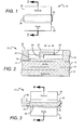
- FIGs. 1 and 2 show one embodiment of a nitride based HEMT 10 according to the present invention that comprises a substrate 12 which can be made of silicon carbide, sapphire, spinet, ZnO, silicon, gallium nitride, aluminum nitride, or any other material capable of supporting growth of a Group-III nitride material.
- the substrate 12 can comprise semiinsulating 4H-SiC commercially available from Cree, Inc. of Durham, NC.
- a nucleation layer 14 can be formed on the substrate 12 to reduce the lattice mismatch between the substrate 12 and the next layer in the HEMT 10.
- the nucleation layer 14 should be approximately 1000 angstroms ( ⁇ ) thick, although other thicknesses can be used.
- Nucleation layer 14 can be formed on the substrate 12 using known semiconductor growth techniques such as metal organic chemical vapor deposition (MOCVD), high vapor pressure epitaxy (HVPE) or molecular beam epitaxy (MBE).
- MOCVD metal organic chemical vapor deposition
- HVPE high vapor pressure epitaxy
- MBE molecular beam epitaxy
- the nucleation layer can be formed as part of another layer in the HEMT 10, such as the buffer layer (described in detail below
- nucleation layer 14 can depend on the material used for the substrate 12. For example, methods of forming a nucleation layer 14 on various substrates are taught in U.S. Patents 5,290,393 and 5,686,738 , each of which are incorporated by reference as if fully set forth herein. Methods of forming nucleation layers on silicon carbide substrates are disclosed in U.S. Patents 5,393,993 , 5,523,589 , and 5,739,554 each of which is incorporated herein by reference as if fully set forth herein.
- the buffer layer 16 comprises a GaN layer that is approximately 2 ⁇ m thick, with part of the layer doped with Fe.
- a barrier layer 18 is formed on the buffer layer 16 such that the buffer layer 16 is sandwiched between the barrier layer 18 and the nucleation layer 14.
- Each of the buffer layer 16 and barrier layer 18 can comprise doped or undoped layers of Group III-nitride materials.
- the barrier layer 18 can comprise one of more layers of different materials such as InGaN, AlGaN, AlN, or combinations thereof.
- the barrier layer 18 comprises 0.8 nm of AlN and 22.5 nm of Al x Ga 1-x N (x ⁇ 0.195, as measured by photo luminescence). Exemplary structures are illustrated in U.S. Patent Nos. 6,316,793 , 6,586,781 , 6,548,333 and U.S. Published Patent Application Nos.
- nitride based HEMT structures are illustrated in U.S. Patents 5,192,987 and 5,296,395 each of which is incorporated herein by reference as if fully set forth herein.
- the buffer and barrier layers 16, 18 can be made using the same methods used to grow the nucleation layer 14.
- a two dimensional electron gas (2DEG) layer/channel 17 is formed at the heterointerface between the buffer and barrier layer 16, 18. Electric isolation between the devices is done with mesa etch or ion implementation outside the active HEMT.
- a spacer layer 24 can be formed on the surface of the barrier layer 18 between the source and drain contacts 20, 22.
- the spacer layer 24 can comprise a layer of non-conducting material such as a dielectric (SiN or SiO), or a number of different layers of non-conducting materials such as different dielectrics.
- the spacer layer can comprise one or more layers of epitaxial material alone or in combination with layers of dielectric material.
- the spacer layer can be many different thicknesses, with a suitable range of thicknesses being approximately 0.05 to 0.5 microns.
- the spacer layer 24 is primarily arranged to allow a field plate to be deposited on it, with the field plate extending from the gate 26 toward the drain contact 22. Accordingly, in some embodiments according to the present invention the spacer layer 24 can be included only on the surface of the barrier layer 18 between the gate 26 and drain contact 22.
- the spacer layer 24 covers the barrier layer 18 between the source and drain contacts 20, 22, the spacer layer 24 can be etched to the barrier layer 18 and a gate electrode 26 deposited such that the bottom of the gate electrode 26 is on the surface of barrier layer 18.
- the gate 26 can be deposited on the barrier layer 18 adjacent to the spacer layer 24. In still other embodiments, the gate 26 can be deposited before the spacer layer 24.
- a field plate 28 can be formed integral to the gate by the metal forming the gate electrode being patterned to extend across spacer layer 24 so that the top of the gate 26 forms a field plate structure 28 extending a distance L f away from the edge of gate 26 towards drain 22. Stated differently, the part of the gate metal resting on the spacer layer 24 forms a field plate 28.
- the structure can then be covered with a dielectric passivation layer 30 such as silicon nitride. Methods of forming the dielectric passivation 30 are described in detail in the patents and publications referenced above.
- the source and drain contacts 20, 22 can be made of different materials including but not limited to alloys of titanium, aluminum, gold or nickel.
- the gate 26 can also be made of different materials including but not limited to gold, nickel, platinum, palladium, iridium, titanium, chromium, alloys of titanium and tungsten, or platinum silicide.
- the gate 26 can have many different lengths, with a suitable range of gate lengths being 0.01 to 2 microns. In one embodiment according to the present invention a preferred gate length (L g ) is approximately 0.5 microns.
- the field plate 28 is formed during the same deposition step as an extension of the gate 26. In other embodiments, the field plate 28 and gate 26 are formed during separate deposition steps. The formation of source and drain contacts 20, 22 is described in detail in the patents and publications referenced above.
- the field plate 28 can extend different distances L f over the barrier layer from the edge of the gate 26 with a suitable range of distances being 0.1 to 1.5 ⁇ m, although other distances can also be used.
- the field plate 28 can comprise many different conductive materials with a suitable material being a metal, such as the same metal used for the gate 26.
- the gate 26 and field plate 28 can be deposited using standard metallization methods.
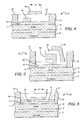
- FIGs. 3 and 4 show another embodiment of a HEMT 40 according to the present invention that is similar to the HEMT 10 in FIGs. 1 and 2 .
- the HEMT 40 comprises a substrate 12, nucleation layer 14, buffer layer 16, 2DEG 17, barrier layer 18, source contact 20, and drain contact 22.
- a gate 42 is formed after formation of the barrier layer 18.
- a spacer/passivation layer 44 is formed on the device and particularly over the gate 42 and the surface of the barrier layer 18 between the gate 42 and the source and drain contacts 20, 22.
- the spacer/passivation layer can be included only over the gate 42 and the surface of the barrier layer 18 between the gate 42 and the drain contact 22.
- a field plate 46 is then formed on the spacer/passivation layer 44 overlapping the gate 42 and extending a distance L f in the gate-drain region.
- the spacer/passivation layer 44 serves as a spacer layer for the field plate 46. The overlap of the field plate 46 over the gate 42 and the distance L f can be varied for optimum results.
- the field plate 46 can be electrically connected to gate 42 and FIG. 3 shows two alternative gate connection structures that can be used, although it is understood that other connection structures can also be used.
- the field plate 46 can be connected to the gate 42 through a first conductive path 48 running outside the active area of the HEMT 40 to a gate contact 50 that is used to make electrical contact to the gate 42.
- a second conductive path 52 (shown in phantom) can also be used that runs outside of the active region of the HEMT 40 on the side opposite the gate contact 50.
- the conductive path 52 is coupled between the gate 42 and the field plate 46.
- Conductive vias (not shown) can also be used to connect the field plate 46 to the gate 42, with each vias running between the two through the passivation layer 44. The vias can be arranged periodically down the field plate 46 to provide for effective current spreading from the gate 42 to the field plate 46.
- the field plate 46 can extend different distances L f over the barrier layer from the edge of the gate 42, with a suitable range of distances being 0.1 to 1.5 ⁇ m, although other distances can also be used. In some embodiments, the field plate 46 can extend a distance L f of 0.2 to 1 ⁇ m. In other embodiments, the field plate 46 can extend a distance L f of 0.5 to 0.9 ⁇ m. In preferred embodiments, the field plate 46 can extend a distance L f of approximately 0.7 ⁇ m.
- FIG. 5 shows another embodiment of a HEMT 60 according to the present invention that has many features similar to those in HEMTs 10 and 40, including a substrate 12, nucleation layer 14, buffer layer 16, 2DEG 17, barrier layer 18, source contact 20, and drain contact 22.
- HEMT 60 has a gamma ( ⁇ ) shaped gate 62 that is particularly adapted to high frequency operation.
- the gate length is one of the important device dimensions in determining the speed of the device, and with higher frequency devices the gate length is shorter. Shorter gate contacts lead to high resistance that can negatively impact high frequency operation.
- T-gates are commonly used in high frequency operation, but it can be difficult to achieve a well-coupled placement of a field plate with a T-gate.
- the gamma gate 62 provides for low gate resistance and allows for controlled definition of the gate footprint.
- a spacer/passivation layer 64 is included that covers the gamma gate 62 and the surface of barrier layer 18 between the gamma gate 62 and the source and drain contacts 20, 22. A space can remain between the horizontal portion of the gamma gate 62 and the top of the spacer layer.
- the HEMT 60 also includes a field plate 66 on the spacer layer 64 that overlaps that gamma gate 62, with the field plate 66 preferably deposited on the side of the gamma gate not having a horizontal overhanging section. This arrangement allows for tight placement and effective coupling between the field plate and the active layers below it.
- the field plate 66 can be electrically connected to the gate 62 in many different ways.
- a first conductive path (not shown) can be included between the field plate 66 and the gate contact or a second conductive path (not shown) can be included between field plate 66 and the gate 62, with both the conductive paths being outside the active area of the HEMT.
- Conductive vias can also be used between the field plate 66 and gate 62 that pass through the spacer layer 64.
- FIG. 6 shows another embodiment of a HEMT 80 according to the present invention that is similar to HEMT 10 shown in FIG. 1 , and also comprises a substrate 12, nucleation layer 14, buffer layer 16, 2DEG 17, barrier layer 18, source contact 20, drain contact 22, spacer layer 24, and gate 26 with a field plate structure 28.
- the HEMT 80 also includes a doped n + contact layer 82 formed on the spacer layer 24. Prior to formation of gate contact 26, contact layer 82 is etched to reveal a portion of the surface of spacer layer 24. A smaller portion of the spacer layer 24 can then be etched down to the barrier layer 18.
- the contact layer 82, spacer layer 24 and barrier layer can also be etched down to the buffer layer 16 so that source and drain contacts 20, 22 can be deposited. Contact layer 82 facilitates formation of ohmic source and drain contacts 20, 22 as well as providing low access region resistances.
- FIG. 7 shows another embodiment of a HEMT 90 according to the present invention having a substrate 12, nucleation layer 14, buffer layer 16, 2DEG 17, barrier layer 18, source contact 20 and drain contact 22 similar to those in the HEMTs described above.
- the HEMT 90 also comprises a gate 92 and a field plate 94.
- the HEMT 90 comprises multiple spacer layers 95, in this case two, although it is understood that more spacer layers can be used.
- a first spacer layer 96 is formed on the barrier layer 18 at least between the gate 92 and the drain contact 22, with a preferred spacer layer also on the barrier layer 18 between the gate 92 and source contact 20.
- a second spacer layer 98 is formed on the first spacer layer 96 and can be arranged in many different ways. It preferably covers less than all of the top surface of the first spacer layer 96 to form a step 100.
- the field plate 94 is formed on the spacer layers, and because of the step 100, the field plate 94 essentially comprises first and second field plates portions 102, 104 each of which has a different spacing between it and the barrier layer 18.
- the first and second spacer layers 96, 98 can comprise many different materials, with the layers typically comprising epitaxial materials or dielectric materials, such as SiN and SiO.
- the first spacer layer 96 can be an epitaxial material and the second spacer layer 98 can be a dielectric material.
- the first spacer layer 96 can again be an epitaxial material, and the second spacer layer 98 can also be an epitaxial material of the same or different material as the first spacer layer 96.
- first spacer layer 96 comprise a dielectric material and the second spacer layer 98 comprise an epitaxial layer, although depending on the type of dielectric material used it can be difficult to form the second (epitaxial) layer 98 because of crystal structure loss.
- Better field plate coupling is typically provided using an epitaxial material, but the capacitance introduced by an epitaxial material can be higher than that of a dielectric material.
- the HEMT 90 can exhibit its improved operating characteristics at two different voltages, with the first field plate 102 allowing improved operation of the HEMT 90 at one voltage and the second field plate 104 allowing improved operation at a higher second voltage.
- the physical dimensions and dielectric constant of the layer 102 under the first field plate 102 is the same. The consistent dimensions and dielectric constant allow for the first field plate to provide improved HEMT 90 operating characteristics at a first voltage.
- the second layer 98 is made of a dielectric material it generally has a lower dielectric constant than the epitaxial material in the first layer 96. As a result, the overall dielectric constant of the material under the second field plate 104 will be lower than the dielectric constant of the material under the first field plate 102. This results in lower capacitance and reduced coupling. The greater distance between the second field plate 104 and the barrier layer 18 along with the lowered dielectric constant results in the second field plate 104 providing improved operating characteristics at a higher voltage.
- the dielectric constant below the first and second field plates 102, 104 remains the same, but the increased distance between the second field plate 104 and barrier layer 18 still provides improved operating characteristics at a higher voltage.
- the higher operating voltage is typically different than it would be if the second spacer layer were a dielectric material.
- the gate 92, field plate 102, 104, and spacer layers 94, 96 can be formed in many different ways, with one formation method being depositing the first (epitaxial) spacer layer 94 on the barrier layer 18 and then etching the barrier layer to provide a space for the gate 92.
- the gate 92 can then be deposited and the second spacer layer 96 can be deposited on the first 96.
- the second spacer layer 96 can be etched before deposition of the gate 92.
- the first and second spacer layers 96, 98 can be deposited on then etched in two etch steps; the first etch through both the layers 96, 98 and the second through the second layer 98 to form the step 100.
- the gate 92 can then be deposited and the field plates 102, 104 can then be deposited over the first spacer and second spacer layers 96, 98.
- the first and second spacer layers 96, 98 can be formed and then etched with the gate 92 and field plates formed in one or more formation steps.
- a single spacer layer of epitaxial or dielectric material can be etched to provide a step such that the resulting field plate has first and second portions.
- FIG. 8, 9 and 10 show HEMTs 110, 130 and 140, respectively, with each HEMT having a substrate 12, nucleation layer 14, buffer layer 16, 2DEG 17, barrier layer 18, source contact 20 and drain contact 22 similar to those in the HEMTs described above.
- the HEMT 110 ( FIG. 8 ) is similar to the HEMT 10 in FIGs. 1 and 2 except that its gate 112 is recessed in the barrier layer 18.
- the HEMT's field plate 114 is deposited on a spacer layer 116 and extend from the gate 112 toward the drain contact 22.
- the field plate 114 provides the same operating improvements as the field plate 28 in HEMT 10.
- HEMT 130 ( FIG. 9 ) is similar to HEMT 40 in FIGs. 3 and 4 except that the gate 132 is recessed.
- the field plate 134 is deposited on a spacer layer 136 and provides the same operating benefits.
- the HEMTs described herein can also comprise gates that are only partially recessed.
- the HEMT 140 is similar to the HEMT 130 except that its gate 142 is partially recessed. Its field plate 144 is deposited on a spacer layer 146 and provides the same operating benefits.
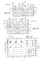
- FIG. 11 shows still another embodiment of a HEMT 150 according to the present invention having a substrate 12, nucleation layer 14, buffer layer 16, 2DEG, 17, barrier layer 18, source contact 20 and drain contact 22.
- the HEMT 150 also has a gate 152, spacer layer 154, and, integral field plate 156.
- the HEMT 150 further comprises a second spacer layer 158 covering the field plate 156, spacer layer 154 and portion of the gate 152 above the spacer layer 154.
- a second field plate 159 is on the second spacer layer 158 extending generally from the gate 152 toward the drain 22, with the second field plate electrically coupled to the gate either by one or more vias (not shown) through the second spacer layer 158, or by one or more conductive paths formed outside of the active region of the HEMT 150.
- Other HEMTs according to the present invention can comprise additional spacer layer and field plate pairs, with one additional pair shown in phantom.
- the structure can also be covered by a dielectric passivation layer (not shown).
- a GaN-based HEMT structure in accordance with the embodiment of FIGs. 3 and 4 was constructed and tested, with the results of the testing shown in the graph 160 of FIG. 12 .
- Initial testing showed a power density of 20.4 W/mm with 51% Power Added Efficiency (PAE) operating in class B at 82V and 4GHz. More recent testing has achieved improved performance with a power density of 32W/mm with 55% PAE at 120V and 4Ghz.
- PAE Power Added Efficiency
- the effect of field plate distance (L f ) on device performance was tested.
- the field plate length L f was varied from a distance of 0 to 0.9 ⁇ m and the PAE of the resulting devices was then measured.
- the PAE showed improvement once the field plate length was extended to 0.5 ⁇ m, with an optimum length of about 0.7 ⁇ m.
- the optimum length may depend on the specific device design as well as operating voltage and frequency.
- FIG. 13 shows one embodiment of a metal semiconductor field effect transistor (MESFET) 170 according to the present invention that is preferably silicon carbide (SiC) based, although MESFETs of other material systems can also be used.
- MESFET 170 comprises a silicon carbide substrate 172 on which a silicon carbide buffer 174 and a silicon carbide channel layer 176 are formed with the buffer 174 sandwiched between the channel layer 176 and substrate 172.
- Source and drain contacts 178, 180 are formed in contact with the channel layer 176.
- a non-conducting spacer layer 182 is formed on the channel layer 176, between the source and drain contacts 178, 180. Similar to the spacer layer 24 described above and shown in FIGs. 1 and 2 , the spacer layer 182 can comprise a layer of non-conducting material such as a dielectric, or a number of different layers of non-conducting materials such as different dielectrics or epitaxial materials.
- the spacer layer 182 can be etched to the channel layer 176 and a gate 184 can be deposited such that the bottom of the gate 184 is on the surface of channel layer 176.
- the metal forming the gate 184 can be patterned to extend across spacer layer 182 so that the top of the gate 184 forms a field plate structure 186 extending a distance L f away from the edge of gate 184 towards drain contact 180.
- the structure can be covered with a dielectric passivation layer 188, such as silicon nitride.
- FIG. 14 shows another embodiment of a MESFET 190 according to the present invention that is similar to MESFET 170 in FIG. 12 , but has a gate and field plate structure similar to that in the HEMT 40 shown in FIGs. 3 and 4 .
- MESFET 190 comprises a silicon carbide substrate 172, buffer 174, and channel 176. It also comprises a source contact 178, drain contact 180, and a gate 192 deposited on the channel 176.
- a spacer layer 194 is deposited over the gate 192 and on the surface of the channel 176 between the gate 192 and the source and drain contacts 178, 180.
- a field plate 186 is deposited on the spacer layer 194 and overlaps the gate 192.
- the field plate 196 is coupled to the gate 192 by a conductive path as described above in HEMT 40 of FIGs. 3 and 4 .
- Many different conductive paths can be used including a first conductive path to the gate contact (not shown) or a second conductive path (not shown) to the gate 192, both of which run outside of the MESFET active area.
- the field 196 can also be coupled to the gate 192 by conductive vias (not shown) through the spacer layer 194.
- FIG. 15 shows one embodiment of a MESFET 200 according to the present invention, with a recessed gate 202. Similar to the MESFETs 170 and 190 shown in FIGs. 12 and 13 , MESFET 200 also has a silicon carbide substrate 172, buffer 174, channel 176, a source contact 178 and a drain contact 180. The gate 202 deposited on the channel 176. A spacer layer 204 is deposited over the gate 202 on the surface of the channel 176 between the gate 202 and the source and drain contacts 178, 180. The spacer layer 204 is thinner than the spacer layer 194 in FIG.
- the gate 202 is partially recessed in the channel 176 and a field plate 206 is deposited on the spacer layer 204, overlapping the gate 202.
- the field plate 206 is coupled to the gate 202 by one or more conductive paths such as those described in HEMT 40 in FIGs. 3 and 4 .
- MESFETs according to the present invention can comprise multiple spacer layers as described HEMT 90 of FIG. 7 .
- the MESFETs can have two spacer layers in a stepped arrangement, although more than two spacer layers can be used.
- the layers can comprise epitaxial or dielectric materials as also described above, with the stepped arrangement effectively providing two field plates that provide improved operating characteristics at two voltages.
- MESFETs according to the present invention can also comprise multiple spacer layers and field plates similar to those on the HEMT 150 shown in FIG. 11 and described above.
Landscapes
- Engineering & Computer Science (AREA)
- Microelectronics & Electronic Packaging (AREA)
- Power Engineering (AREA)
- Physics & Mathematics (AREA)
- Ceramic Engineering (AREA)
- Condensed Matter Physics & Semiconductors (AREA)
- General Physics & Mathematics (AREA)
- Computer Hardware Design (AREA)
- Junction Field-Effect Transistors (AREA)
Applications Claiming Priority (3)
| Application Number | Priority Date | Filing Date | Title |
|---|---|---|---|
| US50157603P | 2003-09-09 | 2003-09-09 | |
| US10/930,160 US7501669B2 (en) | 2003-09-09 | 2004-08-31 | Wide bandgap transistor devices with field plates |
| EP04788642.9A EP1665385B1 (fr) | 2003-09-09 | 2004-09-08 | Dispositifs de transistors a structures de bande larges comprenant des plaques de champs |
Related Parent Applications (2)
| Application Number | Title | Priority Date | Filing Date |
|---|---|---|---|
| EP04788642.9 Division | 2004-09-08 | ||
| EP04788642.9A Division-Into EP1665385B1 (fr) | 2003-09-09 | 2004-09-08 | Dispositifs de transistors a structures de bande larges comprenant des plaques de champs |
Publications (1)
| Publication Number | Publication Date |
|---|---|
| EP2437303A1 true EP2437303A1 (fr) | 2012-04-04 |
Family
ID=34228870
Family Applications (4)
| Application Number | Title | Priority Date | Filing Date |
|---|---|---|---|
| EP04788642.9A Expired - Lifetime EP1665385B1 (fr) | 2003-09-09 | 2004-09-08 | Dispositifs de transistors a structures de bande larges comprenant des plaques de champs |
| EP11183396.8A Expired - Lifetime EP2432021B1 (fr) | 2003-09-09 | 2004-09-08 | Transistor avec plaque de champ. |
| EP11183655A Ceased EP2437303A1 (fr) | 2003-09-09 | 2004-09-08 | Transistor avec plaque de champ. |
| EP11183404A Pending EP2434546A1 (fr) | 2003-09-09 | 2004-09-08 | Transistor avec plaque de champ |
Family Applications Before (2)
| Application Number | Title | Priority Date | Filing Date |
|---|---|---|---|
| EP04788642.9A Expired - Lifetime EP1665385B1 (fr) | 2003-09-09 | 2004-09-08 | Dispositifs de transistors a structures de bande larges comprenant des plaques de champs |
| EP11183396.8A Expired - Lifetime EP2432021B1 (fr) | 2003-09-09 | 2004-09-08 | Transistor avec plaque de champ. |
Family Applications After (1)
| Application Number | Title | Priority Date | Filing Date |
|---|---|---|---|
| EP11183404A Pending EP2434546A1 (fr) | 2003-09-09 | 2004-09-08 | Transistor avec plaque de champ |
Country Status (7)
| Country | Link |
|---|---|
| US (4) | US7501669B2 (fr) |
| EP (4) | EP1665385B1 (fr) |
| JP (1) | JP2007505501A (fr) |
| KR (1) | KR101108300B1 (fr) |
| CN (2) | CN102306658A (fr) |
| CA (1) | CA2536030A1 (fr) |
| WO (1) | WO2005029589A1 (fr) |
Families Citing this family (196)
| Publication number | Priority date | Publication date | Assignee | Title |
|---|---|---|---|---|
| EP2267784B1 (fr) * | 2001-07-24 | 2020-04-29 | Cree, Inc. | HEMT AlGaN/GaN À GRILLE ISOLÉE |
| TWI430341B (zh) * | 2003-09-09 | 2014-03-11 | Univ California | 單一或多重閘極場平板之製造 |
| US7501669B2 (en) | 2003-09-09 | 2009-03-10 | Cree, Inc. | Wide bandgap transistor devices with field plates |
| TWI295085B (en) * | 2003-12-05 | 2008-03-21 | Int Rectifier Corp | Field effect transistor with enhanced insulator structure |
| US7045404B2 (en) * | 2004-01-16 | 2006-05-16 | Cree, Inc. | Nitride-based transistors with a protective layer and a low-damage recess and methods of fabrication thereof |
| US8174048B2 (en) * | 2004-01-23 | 2012-05-08 | International Rectifier Corporation | III-nitride current control device and method of manufacture |
| US7573078B2 (en) | 2004-05-11 | 2009-08-11 | Cree, Inc. | Wide bandgap transistors with multiple field plates |
| US7550783B2 (en) | 2004-05-11 | 2009-06-23 | Cree, Inc. | Wide bandgap HEMTs with source connected field plates |
| US9773877B2 (en) * | 2004-05-13 | 2017-09-26 | Cree, Inc. | Wide bandgap field effect transistors with source connected field plates |
| US20060073621A1 (en) * | 2004-10-01 | 2006-04-06 | Palo Alto Research Center Incorporated | Group III-nitride based HEMT device with insulating GaN/AlGaN buffer layer |
| US9640649B2 (en) * | 2004-12-30 | 2017-05-02 | Infineon Technologies Americas Corp. | III-nitride power semiconductor with a field relaxation feature |
| WO2006080109A1 (fr) * | 2005-01-25 | 2006-08-03 | Fujitsu Limited | Composant a semi-conducteur dote d'une structure mis et son procede de fabrication |
| US11791385B2 (en) * | 2005-03-11 | 2023-10-17 | Wolfspeed, Inc. | Wide bandgap transistors with gate-source field plates |
| US20060223293A1 (en) | 2005-04-01 | 2006-10-05 | Raytheon Company | Semiconductor devices having improved field plates |
| US7615774B2 (en) * | 2005-04-29 | 2009-11-10 | Cree.Inc. | Aluminum free group III-nitride based high electron mobility transistors |
| US20060255377A1 (en) * | 2005-05-12 | 2006-11-16 | Der-Wei Tu | Field effect transistor with novel field-plate structure |
| CN101238560B (zh) * | 2005-06-10 | 2011-08-31 | 日本电气株式会社 | 场效应晶体管 |
| WO2006132418A1 (fr) * | 2005-06-10 | 2006-12-14 | Nec Corporation | Transistor à effet de champ |
| US20070018199A1 (en) * | 2005-07-20 | 2007-01-25 | Cree, Inc. | Nitride-based transistors and fabrication methods with an etch stop layer |
| US7548112B2 (en) * | 2005-07-21 | 2009-06-16 | Cree, Inc. | Switch mode power amplifier using MIS-HEMT with field plate extension |
| US8183595B2 (en) * | 2005-07-29 | 2012-05-22 | International Rectifier Corporation | Normally off III-nitride semiconductor device having a programmable gate |
| JP4751150B2 (ja) | 2005-08-31 | 2011-08-17 | 株式会社東芝 | 窒化物系半導体装置 |
| EP2312635B1 (fr) * | 2005-09-07 | 2020-04-01 | Cree, Inc. | Transistors avec traitement au fluor |
| WO2007136401A2 (fr) * | 2005-09-16 | 2007-11-29 | The Regents Of The University Of California | Transistor à effet de champ à enrichissement, au nitrure de gallium/nitrure d'aluminium et de gallium à polarité n |
| US20070138515A1 (en) * | 2005-12-19 | 2007-06-21 | M/A-Com, Inc. | Dual field plate MESFET |
| DE112007000092B4 (de) * | 2006-01-09 | 2014-07-24 | International Rectifier Corp. | Gruppe-III-Nitrid-Leistungshalbleiter mit einem Feld-Relaxations-Merkmal |
| US7709269B2 (en) | 2006-01-17 | 2010-05-04 | Cree, Inc. | Methods of fabricating transistors including dielectrically-supported gate electrodes |
| US7592211B2 (en) * | 2006-01-17 | 2009-09-22 | Cree, Inc. | Methods of fabricating transistors including supported gate electrodes |
| US7408208B2 (en) * | 2006-03-20 | 2008-08-05 | International Rectifier Corporation | III-nitride power semiconductor device |
| DE112007000667T5 (de) * | 2006-03-20 | 2009-01-29 | International Rectifier Corp., El Segundo | Vereinigter Gate-Kaskoden-Transistor |
| US7388236B2 (en) | 2006-03-29 | 2008-06-17 | Cree, Inc. | High efficiency and/or high power density wide bandgap transistors |
| KR100770132B1 (ko) * | 2006-10-30 | 2007-10-24 | 페어차일드코리아반도체 주식회사 | 질화물계 반도체 소자 |
| EP1921669B1 (fr) * | 2006-11-13 | 2015-09-02 | Cree, Inc. | HEMTs à base de GaN dotés de plaques de champ enterrées |
| US7692263B2 (en) * | 2006-11-21 | 2010-04-06 | Cree, Inc. | High voltage GaN transistors |
| JP4712683B2 (ja) * | 2006-12-21 | 2011-06-29 | パナソニック株式会社 | トランジスタおよびその製造方法 |
| US7838904B2 (en) * | 2007-01-31 | 2010-11-23 | Panasonic Corporation | Nitride based semiconductor device with concave gate region |
| US8212290B2 (en) * | 2007-03-23 | 2012-07-03 | Cree, Inc. | High temperature performance capable gallium nitride transistor |
| JP4691060B2 (ja) * | 2007-03-23 | 2011-06-01 | 古河電気工業株式会社 | GaN系半導体素子 |
| JP5266679B2 (ja) * | 2007-07-11 | 2013-08-21 | 住友電気工業株式会社 | Iii族窒化物電子デバイス |
| US7609115B2 (en) * | 2007-09-07 | 2009-10-27 | Raytheon Company | Input circuitry for transistor power amplifier and method for designing such circuitry |
| US20090072269A1 (en) * | 2007-09-17 | 2009-03-19 | Chang Soo Suh | Gallium nitride diodes and integrated components |
| US7915643B2 (en) * | 2007-09-17 | 2011-03-29 | Transphorm Inc. | Enhancement mode gallium nitride power devices |
| US7800132B2 (en) * | 2007-10-25 | 2010-09-21 | Northrop Grumman Systems Corporation | High electron mobility transistor semiconductor device having field mitigating plate and fabrication method thereof |
| US8039301B2 (en) * | 2007-12-07 | 2011-10-18 | The United States Of America As Represented By The Secretary Of The Navy | Gate after diamond transistor |
| US7750370B2 (en) | 2007-12-20 | 2010-07-06 | Northrop Grumman Space & Mission Systems Corp. | High electron mobility transistor having self-aligned miniature field mitigating plate on a protective dielectric layer |
| JP5134378B2 (ja) * | 2008-01-07 | 2013-01-30 | シャープ株式会社 | 電界効果トランジスタ |
| US7965126B2 (en) | 2008-02-12 | 2011-06-21 | Transphorm Inc. | Bridge circuits and their components |
| US8519438B2 (en) | 2008-04-23 | 2013-08-27 | Transphorm Inc. | Enhancement mode III-N HEMTs |
| CN101604704B (zh) * | 2008-06-13 | 2012-09-05 | 西安能讯微电子有限公司 | Hemt器件及其制造方法 |
| US7985986B2 (en) * | 2008-07-31 | 2011-07-26 | Cree, Inc. | Normally-off semiconductor devices |
| JP5408929B2 (ja) | 2008-08-21 | 2014-02-05 | 昭和電工株式会社 | 半導体装置および半導体装置の製造方法 |
| US8289065B2 (en) | 2008-09-23 | 2012-10-16 | Transphorm Inc. | Inductive load power switching circuits |
| US7898004B2 (en) | 2008-12-10 | 2011-03-01 | Transphorm Inc. | Semiconductor heterostructure diodes |
| US7884394B2 (en) * | 2009-02-09 | 2011-02-08 | Transphorm Inc. | III-nitride devices and circuits |
| US8823012B2 (en) * | 2009-04-08 | 2014-09-02 | Efficient Power Conversion Corporation | Enhancement mode GaN HEMT device with gate spacer and method for fabricating the same |
| US8742459B2 (en) | 2009-05-14 | 2014-06-03 | Transphorm Inc. | High voltage III-nitride semiconductor devices |
| JP5595685B2 (ja) * | 2009-07-28 | 2014-09-24 | パナソニック株式会社 | 半導体装置 |
| US8390000B2 (en) * | 2009-08-28 | 2013-03-05 | Transphorm Inc. | Semiconductor devices with field plates |
| US8138529B2 (en) | 2009-11-02 | 2012-03-20 | Transphorm Inc. | Package configurations for low EMI circuits |
| JP5625336B2 (ja) * | 2009-11-30 | 2014-11-19 | サンケン電気株式会社 | 半導体装置 |
| JP5037594B2 (ja) * | 2009-12-08 | 2012-09-26 | シャープ株式会社 | 電界効果トランジスタ |
| US8389977B2 (en) * | 2009-12-10 | 2013-03-05 | Transphorm Inc. | Reverse side engineered III-nitride devices |
| US8816497B2 (en) * | 2010-01-08 | 2014-08-26 | Transphorm Inc. | Electronic devices and components for high efficiency power circuits |
| US8624662B2 (en) * | 2010-02-05 | 2014-01-07 | Transphorm Inc. | Semiconductor electronic components and circuits |
| US20110241020A1 (en) * | 2010-03-31 | 2011-10-06 | Triquint Semiconductor, Inc. | High electron mobility transistor with recessed barrier layer |
| US8907350B2 (en) * | 2010-04-28 | 2014-12-09 | Cree, Inc. | Semiconductor devices having improved adhesion and methods of fabricating the same |
| EP2383786B1 (fr) | 2010-04-29 | 2018-08-15 | Ampleon Netherlands B.V. | Transistor à semi-conducteur comportant deux éléments d'écran électriquement conducteurs |
| US8829999B2 (en) | 2010-05-20 | 2014-09-09 | Cree, Inc. | Low noise amplifiers including group III nitride based high electron mobility transistors |
| JP2011249728A (ja) * | 2010-05-31 | 2011-12-08 | Toshiba Corp | 半導体装置および半導体装置の製造方法 |
| CN103026491B (zh) * | 2010-07-06 | 2016-03-02 | 香港科技大学 | 常关断型三族氮化物金属-二维电子气隧穿结场效应晶体管 |
| JP5655424B2 (ja) * | 2010-08-09 | 2015-01-21 | サンケン電気株式会社 | 化合物半導体装置 |
| JP2012109492A (ja) * | 2010-11-19 | 2012-06-07 | Sanken Electric Co Ltd | 化合物半導体装置 |
| JP5707903B2 (ja) * | 2010-12-02 | 2015-04-30 | 富士通株式会社 | 化合物半導体装置及びその製造方法 |
| US8742460B2 (en) | 2010-12-15 | 2014-06-03 | Transphorm Inc. | Transistors with isolation regions |
| US8643062B2 (en) | 2011-02-02 | 2014-02-04 | Transphorm Inc. | III-N device structures and methods |
| US8786327B2 (en) | 2011-02-28 | 2014-07-22 | Transphorm Inc. | Electronic components with reactive filters |
| US8772842B2 (en) | 2011-03-04 | 2014-07-08 | Transphorm, Inc. | Semiconductor diodes with low reverse bias currents |
| US8716141B2 (en) | 2011-03-04 | 2014-05-06 | Transphorm Inc. | Electrode configurations for semiconductor devices |
| US8803232B2 (en) | 2011-05-29 | 2014-08-12 | Taiwan Semiconductor Manufacturing Co., Ltd. | High voltage and ultra-high voltage semiconductor devices with increased breakdown voltages |
| US8901604B2 (en) | 2011-09-06 | 2014-12-02 | Transphorm Inc. | Semiconductor devices with guard rings |
| US9257547B2 (en) | 2011-09-13 | 2016-02-09 | Transphorm Inc. | III-N device structures having a non-insulating substrate |
| US8772833B2 (en) * | 2011-09-21 | 2014-07-08 | Electronics And Telecommunications Research Institute | Power semiconductor device and fabrication method thereof |
| US8598937B2 (en) | 2011-10-07 | 2013-12-03 | Transphorm Inc. | High power semiconductor electronic components with increased reliability |
| US20130105817A1 (en) | 2011-10-26 | 2013-05-02 | Triquint Semiconductor, Inc. | High electron mobility transistor structure and method |
| US8884308B2 (en) | 2011-11-29 | 2014-11-11 | Taiwan Semiconductor Manufacturing Company, Ltd. | High electron mobility transistor structure with improved breakdown voltage performance |
| US9209176B2 (en) | 2011-12-07 | 2015-12-08 | Transphorm Inc. | Semiconductor modules and methods of forming the same |
| US10002957B2 (en) * | 2011-12-21 | 2018-06-19 | Power Integrations, Inc. | Shield wrap for a heterostructure field effect transistor |
| JP2013131650A (ja) * | 2011-12-21 | 2013-07-04 | Fujitsu Ltd | 半導体装置及びその製造方法 |
| US9165766B2 (en) | 2012-02-03 | 2015-10-20 | Transphorm Inc. | Buffer layer structures suited for III-nitride devices with foreign substrates |
| TWI566402B (zh) * | 2012-02-23 | 2017-01-11 | 高效電源轉換公司 | 具有閘極間隔件之增強模式氮化鎵高電子遷移率電晶體元件及其製造方法 |
| US8648643B2 (en) | 2012-02-24 | 2014-02-11 | Transphorm Inc. | Semiconductor power modules and devices |
| US9093366B2 (en) | 2012-04-09 | 2015-07-28 | Transphorm Inc. | N-polar III-nitride transistors |
| US9443941B2 (en) | 2012-06-04 | 2016-09-13 | Infineon Technologies Austria Ag | Compound semiconductor transistor with self aligned gate |
| US9184275B2 (en) | 2012-06-27 | 2015-11-10 | Transphorm Inc. | Semiconductor devices with integrated hole collectors |
| US8803246B2 (en) | 2012-07-16 | 2014-08-12 | Transphorm Inc. | Semiconductor electronic components with integrated current limiters |
| JP6085442B2 (ja) | 2012-09-28 | 2017-02-22 | トランスフォーム・ジャパン株式会社 | 化合物半導体装置及びその製造方法 |
| WO2014050054A1 (fr) * | 2012-09-28 | 2014-04-03 | パナソニック株式会社 | Dispositif à semi-conducteur |
| JP2014090037A (ja) * | 2012-10-29 | 2014-05-15 | Advanced Power Device Research Association | 半導体装置 |
| US9171730B2 (en) | 2013-02-15 | 2015-10-27 | Transphorm Inc. | Electrodes for semiconductor devices and methods of forming the same |
| US9087718B2 (en) | 2013-03-13 | 2015-07-21 | Transphorm Inc. | Enhancement-mode III-nitride devices |
| US9245992B2 (en) | 2013-03-15 | 2016-01-26 | Transphorm Inc. | Carbon doping semiconductor devices |
| US9048184B2 (en) * | 2013-03-15 | 2015-06-02 | Northrop Grumman Systems Corporation | Method of forming a gate contact |
| US9059076B2 (en) | 2013-04-01 | 2015-06-16 | Transphorm Inc. | Gate drivers for circuits based on semiconductor devices |
| US9202880B1 (en) | 2013-04-23 | 2015-12-01 | Hrl Laboratories, Llc | Etch-based fabrication process for stepped field-plate wide-bandgap |
| US9755059B2 (en) | 2013-06-09 | 2017-09-05 | Cree, Inc. | Cascode structures with GaN cap layers |
| US9847411B2 (en) * | 2013-06-09 | 2017-12-19 | Cree, Inc. | Recessed field plate transistor structures |
| US9679981B2 (en) | 2013-06-09 | 2017-06-13 | Cree, Inc. | Cascode structures for GaN HEMTs |
| US9407214B2 (en) | 2013-06-28 | 2016-08-02 | Cree, Inc. | MMIC power amplifier |
| WO2015006111A1 (fr) | 2013-07-09 | 2015-01-15 | Transphorm Inc. | Onduleurs multiniveaux et leurs composants |
| US9455341B2 (en) * | 2013-07-17 | 2016-09-27 | Taiwan Semiconductor Manufacturing Company, Ltd. | Transistor having a back-barrier layer and method of making the same |
| US9443938B2 (en) | 2013-07-19 | 2016-09-13 | Transphorm Inc. | III-nitride transistor including a p-type depleting layer |
| TWI555209B (zh) * | 2013-07-29 | 2016-10-21 | 高效電源轉換公司 | 具有降低的輸出電容之氮化鎵裝置及其製法 |
| US10566429B2 (en) * | 2013-08-01 | 2020-02-18 | Dynax Semiconductor, Inc. | Semiconductor device and method of manufacturing the same |
| US10665709B2 (en) | 2013-09-10 | 2020-05-26 | Delta Electronics, Inc. | Power semiconductor device integrated with ESD protection circuit under source pad, drain pad, and/or gate pad |
| US10833185B2 (en) | 2013-09-10 | 2020-11-10 | Delta Electronics, Inc. | Heterojunction semiconductor device having source and drain pads with improved current crowding |
| US10910491B2 (en) | 2013-09-10 | 2021-02-02 | Delta Electronics, Inc. | Semiconductor device having reduced capacitance between source and drain pads |
| US10236236B2 (en) | 2013-09-10 | 2019-03-19 | Delta Electronics, Inc. | Heterojunction semiconductor device for reducing parasitic capacitance |
| TWI577022B (zh) | 2014-02-27 | 2017-04-01 | 台達電子工業股份有限公司 | 半導體裝置與應用其之半導體裝置封裝體 |
| KR102100928B1 (ko) * | 2013-10-17 | 2020-05-15 | 삼성전자주식회사 | 고전자 이동도 트랜지스터 |
| JP2015177016A (ja) * | 2014-03-14 | 2015-10-05 | 株式会社東芝 | 半導体装置 |
| US8980759B1 (en) | 2014-05-22 | 2015-03-17 | Hrl Laboratories, Llc | Method of fabricating slanted field-plate GaN heterojunction field-effect transistor |
| US9543940B2 (en) | 2014-07-03 | 2017-01-10 | Transphorm Inc. | Switching circuits having ferrite beads |
| US9590494B1 (en) | 2014-07-17 | 2017-03-07 | Transphorm Inc. | Bridgeless power factor correction circuits |
| US9318593B2 (en) | 2014-07-21 | 2016-04-19 | Transphorm Inc. | Forming enhancement mode III-nitride devices |
| EP3195364A4 (fr) | 2014-09-18 | 2018-04-25 | Intel Corporation | Structures hétéroépitaxiales de wurtzite à facettes de paroi latérale inclinées pour commande de propagation de défauts dans des dispositifs semi-conducteurs de silicium compatibles avec semi-conducteur complémentaire à l'oxyde de métal (cmos ) |
| US10229991B2 (en) | 2014-09-25 | 2019-03-12 | Intel Corporation | III-N epitaxial device structures on free standing silicon mesas |
| US9640623B2 (en) | 2014-10-17 | 2017-05-02 | Cree, Inc. | Semiconductor device with improved field plate |
| US9608078B2 (en) | 2014-10-17 | 2017-03-28 | Cree, Inc. | Semiconductor device with improved field plate |
| CN106796953B (zh) * | 2014-10-30 | 2021-03-30 | 英特尔公司 | 源极/漏极至氮化镓晶体管中的2d电子气的低接触电阻再生长 |
| US9590087B2 (en) | 2014-11-13 | 2017-03-07 | Infineon Technologies Austria Ag | Compound gated semiconductor device having semiconductor field plate |
| US9559161B2 (en) * | 2014-11-13 | 2017-01-31 | Infineon Technologies Austria Ag | Patterned back-barrier for III-nitride semiconductor devices |
| US9536967B2 (en) | 2014-12-16 | 2017-01-03 | Transphorm Inc. | Recessed ohmic contacts in a III-N device |
| US9536966B2 (en) | 2014-12-16 | 2017-01-03 | Transphorm Inc. | Gate structures for III-N devices |
| KR102309482B1 (ko) | 2014-12-18 | 2021-10-07 | 인텔 코포레이션 | N-채널 갈륨 질화물 트랜지스터들 |
| JP2016171162A (ja) * | 2015-03-12 | 2016-09-23 | 株式会社東芝 | 半導体装置 |
| US10200030B2 (en) | 2015-03-13 | 2019-02-05 | Transphorm Inc. | Paralleling of switching devices for high power circuits |
| CN104882483B (zh) * | 2015-05-05 | 2018-06-26 | 西安电子科技大学 | 具有γ栅和凹陷缓冲层的场效应晶体管及其制备方法 |
| CN104916684B (zh) * | 2015-06-11 | 2018-04-27 | 大连理工大学 | 一种纵向短开启栅极沟道型hemt器件及其制备方法 |
| US9911817B2 (en) | 2015-07-17 | 2018-03-06 | Cambridge Electronics, Inc. | Field-plate structures for semiconductor devices |
| US10553689B2 (en) | 2015-12-23 | 2020-02-04 | Intel Corporation | Multiple stacked field-plated GaN transistor and interlayer dielectrics to improve breakdown voltage and reduce parasitic capacitances |
| JP6888013B2 (ja) | 2016-01-15 | 2021-06-16 | トランスフォーム テクノロジー,インコーポレーテッド | AL(1−x)Si(x)Oゲート絶縁体を有するエンハンスメントモードIII族窒化物デバイス |
| WO2017210323A1 (fr) | 2016-05-31 | 2017-12-07 | Transphorm Inc. | Dispositifs au nitrure du groupe iii comprenant une couche d'appauvrissement à gradient |
| TWI684278B (zh) | 2016-06-01 | 2020-02-01 | 美商高效電源轉換公司 | 多步驟表面鈍化結構及用於製造其之方法 |
| DE102016122399A1 (de) * | 2016-11-21 | 2018-05-24 | Forschungsverbund Berlin E.V. | Gate-Struktur und Verfahren zu dessen Herstellung |
| DE102016123931A1 (de) | 2016-12-09 | 2018-06-14 | United Monolithic Semiconductors Gmbh | Transistor |
| DE102016123934A1 (de) | 2016-12-09 | 2018-06-14 | United Monolithic Semiconductors Gmbh | Verfahren zur Herstellung eines Transistors |
| CN107068740B (zh) * | 2017-03-29 | 2019-12-03 | 西安电子科技大学 | 源阶梯场板垂直型功率晶体管 |
| CN107134490B (zh) * | 2017-03-29 | 2020-04-14 | 西安电子科技大学 | 基于弧形源场板和弧形漏场板的垂直型功率器件及其制作方法 |
| CN107170820B (zh) * | 2017-03-29 | 2020-04-14 | 西安电子科技大学 | 弧形栅-漏复合场板电流孔径异质结器件 |
| CN107134491B (zh) * | 2017-03-29 | 2019-11-29 | 西安电子科技大学 | 基于弧形源场板的垂直结构电力电子器件 |
| US10319648B2 (en) | 2017-04-17 | 2019-06-11 | Transphorm Inc. | Conditions for burn-in of high power semiconductors |
| US11233053B2 (en) | 2017-09-29 | 2022-01-25 | Intel Corporation | Group III-nitride (III-N) devices with reduced contact resistance and their methods of fabrication |
| US10326002B1 (en) * | 2018-06-11 | 2019-06-18 | Globalfoundries Inc. | Self-aligned gate contact and cross-coupling contact formation |
| FR3088485B1 (fr) * | 2018-11-13 | 2021-04-30 | Commissariat Energie Atomique | Dispositif semi-conducteur a plaque de champ |
| CN109887836B (zh) * | 2019-01-25 | 2021-03-02 | 西安交通大学 | n型掺杂单晶金刚石场板结构的场效应晶体管的制备方法 |
| US11121245B2 (en) | 2019-02-22 | 2021-09-14 | Efficient Power Conversion Corporation | Field plate structures with patterned surface passivation layers and methods for manufacturing thereof |
| CN110010682B (zh) * | 2019-03-22 | 2024-08-02 | 华南理工大学 | 具有三明治结构的GaN-HEMT器件及其制备方法 |
| US10971612B2 (en) | 2019-06-13 | 2021-04-06 | Cree, Inc. | High electron mobility transistors and power amplifiers including said transistors having improved performance and reliability |
| CN110581170A (zh) * | 2019-08-13 | 2019-12-17 | 中山市华南理工大学现代产业技术研究院 | 具有Г型栅的GaN基MIS-HEMT器件及制备方法 |
| US12032014B2 (en) | 2019-09-09 | 2024-07-09 | Analog Devices International Unlimited Company | Semiconductor device configured for gate dielectric monitoring |
| US11862691B2 (en) | 2019-11-01 | 2024-01-02 | Raytheon Company | Field effect transistor having field plate |
| US11552190B2 (en) * | 2019-12-12 | 2023-01-10 | Analog Devices International Unlimited Company | High voltage double-diffused metal oxide semiconductor transistor with isolated parasitic bipolar junction transistor region |
| CN113875019B (zh) * | 2020-04-30 | 2024-07-02 | 英诺赛科(苏州)半导体有限公司 | 半导体器件以及制造半导体器件的方法 |
| US11769768B2 (en) | 2020-06-01 | 2023-09-26 | Wolfspeed, Inc. | Methods for pillar connection on frontside and passive device integration on backside of die |
| US11228287B2 (en) | 2020-06-17 | 2022-01-18 | Cree, Inc. | Multi-stage decoupling networks integrated with on-package impedance matching networks for RF power amplifiers |
| US11533025B2 (en) | 2020-06-18 | 2022-12-20 | Wolfspeed, Inc. | Integrated doherty amplifier with added isolation between the carrier and the peaking transistors |
| US11581859B2 (en) | 2020-06-26 | 2023-02-14 | Wolfspeed, Inc. | Radio frequency (RF) transistor amplifier packages with improved isolation and lead configurations |
| US11887945B2 (en) | 2020-09-30 | 2024-01-30 | Wolfspeed, Inc. | Semiconductor device with isolation and/or protection structures |
| US11658234B2 (en) | 2020-10-27 | 2023-05-23 | Wolfspeed, Inc. | Field effect transistor with enhanced reliability |
| US11502178B2 (en) | 2020-10-27 | 2022-11-15 | Wolfspeed, Inc. | Field effect transistor with at least partially recessed field plate |
| US11749726B2 (en) | 2020-10-27 | 2023-09-05 | Wolfspeed, Inc. | Field effect transistor with source-connected field plate |
| EP4244890A1 (fr) | 2020-11-13 | 2023-09-20 | Wolfspeed, Inc. | Dispositif d'alimentation rf en boîtier avec acheminement de pcb |
| CN112771678B (zh) * | 2020-12-25 | 2023-05-02 | 英诺赛科(苏州)科技有限公司 | 半导体器件及其制造方法 |
| WO2022134018A1 (fr) * | 2020-12-25 | 2022-06-30 | Innoscience (Suzhou) Technology Co., Ltd. | Dispositif à semi-conducteur et son procédé de fabrication |
| CN113016074B (zh) * | 2021-02-19 | 2022-08-12 | 英诺赛科(苏州)科技有限公司 | 半导体器件 |
| CN113053749B (zh) * | 2021-03-12 | 2022-06-21 | 浙江大学 | GaN器件及制备方法 |
| WO2022212327A1 (fr) * | 2021-03-31 | 2022-10-06 | Massachusetts Institute Of Technology | Dispositif à semi-conducteur pourvu de structures de gestion de champ électrique |
| US12009417B2 (en) | 2021-05-20 | 2024-06-11 | Macom Technology Solutions Holdings, Inc. | High electron mobility transistors having improved performance |
| US20220376104A1 (en) | 2021-05-20 | 2022-11-24 | Cree, Inc. | Transistors including semiconductor surface modification and related fabrication methods |
| US12015075B2 (en) | 2021-05-20 | 2024-06-18 | Macom Technology Solutions Holdings, Inc. | Methods of manufacturing high electron mobility transistors having a modified interface region |
| US11869964B2 (en) | 2021-05-20 | 2024-01-09 | Wolfspeed, Inc. | Field effect transistors with modified access regions |
| US11842937B2 (en) | 2021-07-30 | 2023-12-12 | Wolfspeed, Inc. | Encapsulation stack for improved humidity performance and related fabrication methods |
| WO2023013431A1 (fr) * | 2021-08-03 | 2023-02-09 | ヌヴォトンテクノロジージャパン株式会社 | Élément à capacité variable |
| US11621672B2 (en) | 2021-08-05 | 2023-04-04 | Wolfspeed, Inc. | Compensation of trapping in field effect transistors |
| US20230075505A1 (en) | 2021-09-03 | 2023-03-09 | Wolfspeed, Inc. | Metal pillar connection topologies for heterogeneous packaging |
| US20230078017A1 (en) | 2021-09-16 | 2023-03-16 | Wolfspeed, Inc. | Semiconductor device incorporating a substrate recess |
| WO2024037906A1 (fr) * | 2022-08-15 | 2024-02-22 | Signify Holding B.V. | Noeud de commutation en demi-pont protégé d'une tension d'entrée et d'une masse |
| US20240105823A1 (en) | 2022-09-23 | 2024-03-28 | Wolfspeed, Inc. | Barrier Structure for Dispersion Reduction in Transistor Devices |
| US20240105824A1 (en) | 2022-09-23 | 2024-03-28 | Wolfspeed, Inc. | Barrier Structure for Sub-100 Nanometer Gate Length Devices |
| US20240106397A1 (en) | 2022-09-23 | 2024-03-28 | Wolfspeed, Inc. | Transistor amplifier with pcb routing and surface mounted transistor die |
| US20240120202A1 (en) | 2022-10-06 | 2024-04-11 | Wolfspeed, Inc. | Implanted Regions for Semiconductor Structures with Deep Buried Layers |
| US20240266426A1 (en) | 2023-02-03 | 2024-08-08 | Wolfspeed, Inc. | Semiconductor Structure for Improved Radio Frequency Thermal Management |
| US20240266419A1 (en) | 2023-02-03 | 2024-08-08 | Wolfspeed, Inc. | Semiconductor Device Having Semiconductor Structure with Polarity Inverting Layer |
| US20240304702A1 (en) | 2023-03-06 | 2024-09-12 | Wolfspeed, Inc. | Field Reducing Structures for Nitrogen-Polar Group III-Nitride Semiconductor Devices |
| CN118099209A (zh) * | 2024-04-28 | 2024-05-28 | 英诺赛科(苏州)半导体有限公司 | 一种GaN功率器件及其制备方法 |
| CN118367014A (zh) * | 2024-06-18 | 2024-07-19 | 河源市众拓光电科技有限公司 | 一种GaN基HEMT器件及其制备方法 |
Citations (16)
| Publication number | Priority date | Publication date | Assignee | Title |
|---|---|---|---|---|
| US5192987A (en) | 1991-05-17 | 1993-03-09 | Apa Optics, Inc. | High electron mobility transistor with GaN/Alx Ga1-x N heterojunctions |
| US5290393A (en) | 1991-01-31 | 1994-03-01 | Nichia Kagaku Kogyo K.K. | Crystal growth method for gallium nitride-based compound semiconductor |
| US5393993A (en) | 1993-12-13 | 1995-02-28 | Cree Research, Inc. | Buffer structure between silicon carbide and gallium nitride and resulting semiconductor devices |
| US5523589A (en) | 1994-09-20 | 1996-06-04 | Cree Research, Inc. | Vertical geometry light emitting diode with group III nitride active layer and extended lifetime |
| US5686738A (en) | 1991-03-18 | 1997-11-11 | Trustees Of Boston University | Highly insulating monocrystalline gallium nitride thin films |
| US5686737A (en) | 1994-09-16 | 1997-11-11 | Cree Research, Inc. | Self-aligned field-effect transistor for high frequency applications |
| US5739554A (en) | 1995-05-08 | 1998-04-14 | Cree Research, Inc. | Double heterojunction light emitting diode with gallium nitride active layer |
| US6033948A (en) * | 1995-12-02 | 2000-03-07 | Lg Semicon Co., Ltd. | Method of making high voltage metal oxide silicon field effect transistor |
| US6100571A (en) * | 1998-06-16 | 2000-08-08 | Nec Corporation | Fet having non-overlapping field control electrode between gate and drain |
| US6316793B1 (en) | 1998-06-12 | 2001-11-13 | Cree, Inc. | Nitride based transistors on semi-insulating silicon carbide substrates |
| US20020005528A1 (en) * | 2000-07-17 | 2002-01-17 | Fujitsu Quantum Devices Limited | High-speed compound semiconductor device operable at large output power with minimum leakage current |
| US20020167023A1 (en) | 2001-05-11 | 2002-11-14 | Cree Lighting Company And Regents Of The University Of California | Group-III nitride based high electron mobility transistor (HEMT) with barrier/spacer layer |
| US6483135B1 (en) * | 1998-09-22 | 2002-11-19 | Nec Compound Semiconductor Devices, Ltd. | Field effect transistor |
| US20030020092A1 (en) | 2001-07-24 | 2003-01-30 | Primit Parikh | Insulating gate AlGaN/GaN HEMT |
| US6548333B2 (en) | 2000-12-01 | 2003-04-15 | Cree, Inc. | Aluminum gallium nitride/gallium nitride high electron mobility transistors having a gate contact on a gallium nitride based cap segment |
| US6586781B2 (en) | 2000-02-04 | 2003-07-01 | Cree Lighting Company | Group III nitride based FETs and HEMTs with reduced trapping and method for producing the same |
Family Cites Families (151)
| Publication number | Priority date | Publication date | Assignee | Title |
|---|---|---|---|---|
| US5187552A (en) | 1979-03-28 | 1993-02-16 | Hendrickson Thomas E | Shielded field-effect transistor devices |
| US4947232A (en) * | 1980-03-22 | 1990-08-07 | Sharp Kabushiki Kaisha | High voltage MOS transistor |
| JPS56169368A (en) * | 1980-05-30 | 1981-12-26 | Sharp Corp | High withstand voltage mos field effect semiconductor device |
| NL8103218A (nl) | 1981-07-06 | 1983-02-01 | Philips Nv | Veldeffekttransistor met geisoleerde stuurelektrode. |
| US4551905A (en) * | 1982-12-09 | 1985-11-12 | Cornell Research Foundation, Inc. | Fabrication of metal lines for semiconductor devices |
| JPS59104706U (ja) | 1982-12-29 | 1984-07-14 | オカモト株式会社 | 手袋成形型 |
| JPS62237763A (ja) | 1986-04-08 | 1987-10-17 | Agency Of Ind Science & Technol | 半導体装置の製造方法 |
| JPH0514463Y2 (fr) | 1986-11-27 | 1993-04-16 | ||
| US5196359A (en) * | 1988-06-30 | 1993-03-23 | Texas Instruments Incorporated | Method of forming heterostructure field effect transistor |
| JPH0738108B2 (ja) | 1988-11-28 | 1995-04-26 | ヤマハ株式会社 | 電子楽器の楽音制御方法 |
| JPH0750413Y2 (ja) | 1991-02-25 | 1995-11-15 | 石川島播磨重工業株式会社 | フラップ式保安ゲート |
| JPH0521793A (ja) | 1991-07-09 | 1993-01-29 | Mitsubishi Electric Corp | 半導体装置及びその製造方法 |
| JPH06204253A (ja) | 1993-01-07 | 1994-07-22 | Fujitsu Ltd | 電界効果半導体装置 |
| JPH06224225A (ja) * | 1993-01-27 | 1994-08-12 | Fujitsu Ltd | 電界効果半導体装置 |
| JP3188346B2 (ja) | 1993-06-10 | 2001-07-16 | ローム株式会社 | 電界効果トランジスタ |
| JP2658860B2 (ja) | 1993-12-20 | 1997-09-30 | 日本電気株式会社 | 半導体装置およびその製造方法 |
| US5543253A (en) | 1994-08-08 | 1996-08-06 | Electronics & Telecommunications Research Inst. | Photomask for t-gate formation and process for fabricating the same |
| JP3051817B2 (ja) | 1995-01-31 | 2000-06-12 | シャープ株式会社 | 半導体装置の製造方法 |
| US6002148A (en) * | 1995-06-30 | 1999-12-14 | Motorola, Inc. | Silicon carbide transistor and method |
| US5569937A (en) * | 1995-08-28 | 1996-10-29 | Motorola | High breakdown voltage silicon carbide transistor |
| US6720615B2 (en) * | 1996-01-22 | 2004-04-13 | Fuji Electric Co., Ltd. | Vertical-type MIS semiconductor device |
| TW360982B (en) | 1996-01-26 | 1999-06-11 | Matsushita Electric Works Ltd | Thin film transistor of silicon-on-insulator type |
| JPH09232827A (ja) | 1996-02-21 | 1997-09-05 | Oki Electric Ind Co Ltd | 半導体装置及び送受信切り替え型アンテナスイッチ回路 |
| US5652179A (en) * | 1996-04-24 | 1997-07-29 | Watkins-Johnson Company | Method of fabricating sub-micron gate electrode by angle and direct evaporation |
| US5710455A (en) | 1996-07-29 | 1998-01-20 | Motorola | Lateral MOSFET with modified field plates and damage areas |
| US5929467A (en) * | 1996-12-04 | 1999-07-27 | Sony Corporation | Field effect transistor with nitride compound |
| JP3958404B2 (ja) * | 1997-06-06 | 2007-08-15 | 三菱電機株式会社 | 横型高耐圧素子を有する半導体装置 |
| JPH118256A (ja) | 1997-06-13 | 1999-01-12 | Oki Electric Ind Co Ltd | 電界効果トランジスタの製造方法 |
| JP4028897B2 (ja) * | 1997-07-24 | 2007-12-26 | 三菱電機株式会社 | 電界効果半導体装置 |
| TW334632B (en) | 1997-07-24 | 1998-06-21 | Mitsubishi Electric Corp | Field effective semiconductor |
| JP3457511B2 (ja) * | 1997-07-30 | 2003-10-20 | 株式会社東芝 | 半導体装置及びその製造方法 |
| US5898198A (en) | 1997-08-04 | 1999-04-27 | Spectrian | RF power device having voltage controlled linearity |
| US6346451B1 (en) * | 1997-12-24 | 2002-02-12 | Philips Electronics North America Corporation | Laterial thin-film silicon-on-insulator (SOI) device having a gate electrode and a field plate electrode |
| DE19800647C1 (de) * | 1998-01-09 | 1999-05-27 | Siemens Ag | SOI-Hochspannungsschalter |
| JP3127874B2 (ja) | 1998-02-12 | 2001-01-29 | 日本電気株式会社 | 電界効果トランジスタ及びその製造方法 |
| JP3233207B2 (ja) | 1998-03-20 | 2001-11-26 | 日本電気株式会社 | 電界効果トランジスタの製造方法 |
| JP3534624B2 (ja) | 1998-05-01 | 2004-06-07 | 沖電気工業株式会社 | 半導体装置の製造方法 |
| JP2000082671A (ja) | 1998-06-26 | 2000-03-21 | Sony Corp | 窒化物系iii−v族化合物半導体装置とその製造方法 |
| US6042975A (en) | 1998-07-08 | 2000-03-28 | Lucent Technologies Inc. | Alignment techniques for photolithography utilizing multiple photoresist layers |
| DE19835454A1 (de) * | 1998-08-05 | 2000-02-10 | Aventis Res & Tech Gmbh & Co | Geschütztes supraleitendes Bauteil und Verfahren zu dessen Herstellung |
| US6100549A (en) | 1998-08-12 | 2000-08-08 | Motorola, Inc. | High breakdown voltage resurf HFET |
| JP2000164926A (ja) | 1998-11-24 | 2000-06-16 | Sony Corp | 化合物半導体の選択エッチング方法、窒化物系化合物半導体の選択エッチング方法、半導体装置および半導体装置の製造方法 |
| US6495409B1 (en) * | 1999-01-26 | 2002-12-17 | Agere Systems Inc. | MOS transistor having aluminum nitride gate structure and method of manufacturing same |
| JP3497406B2 (ja) | 1999-03-25 | 2004-02-16 | 株式会社クボタ | 水田作業機 |
| US6127703A (en) * | 1999-08-31 | 2000-10-03 | Philips Electronics North America Corporation | Lateral thin-film silicon-on-insulator (SOI) PMOS device having a drain extension region |
| JP2001160656A (ja) | 1999-12-01 | 2001-06-12 | Sharp Corp | 窒化物系化合物半導体装置 |
| US6639255B2 (en) | 1999-12-08 | 2003-10-28 | Matsushita Electric Industrial Co., Ltd. | GaN-based HFET having a surface-leakage reducing cap layer |
| JP4592938B2 (ja) * | 1999-12-08 | 2010-12-08 | パナソニック株式会社 | 半導体装置 |
| JP2001189324A (ja) | 1999-12-28 | 2001-07-10 | Ricoh Co Ltd | 半導体装置 |
| US6686616B1 (en) * | 2000-05-10 | 2004-02-03 | Cree, Inc. | Silicon carbide metal-semiconductor field effect transistors |
| JP4186032B2 (ja) * | 2000-06-29 | 2008-11-26 | 日本電気株式会社 | 半導体装置 |
| JP4198339B2 (ja) | 2000-07-17 | 2008-12-17 | ユーディナデバイス株式会社 | 化合物半導体装置 |
| US6624488B1 (en) * | 2000-08-07 | 2003-09-23 | Advanced Micro Devices, Inc. | Epitaxial silicon growth and usage of epitaxial gate insulator for low power, high performance devices |
| JP4322414B2 (ja) | 2000-09-19 | 2009-09-02 | 株式会社ルネサステクノロジ | 半導体装置 |
| US6690042B2 (en) * | 2000-09-27 | 2004-02-10 | Sensor Electronic Technology, Inc. | Metal oxide semiconductor heterostructure field effect transistor |
| JP2002118122A (ja) | 2000-10-06 | 2002-04-19 | Nec Corp | ショットキゲート電界効果トランジスタ |
| US6891235B1 (en) | 2000-11-15 | 2005-05-10 | International Business Machines Corporation | FET with T-shaped gate |
| TWI288435B (en) | 2000-11-21 | 2007-10-11 | Matsushita Electric Ind Co Ltd | Semiconductor device and equipment for communication system |
| JP2001230263A (ja) | 2001-01-29 | 2001-08-24 | Nec Corp | 電界効果型トランジスタ |
| US6791119B2 (en) | 2001-02-01 | 2004-09-14 | Cree, Inc. | Light emitting diodes including modifications for light extraction |
| US6468878B1 (en) * | 2001-02-27 | 2002-10-22 | Koninklijke Philips Electronics N.V. | SOI LDMOS structure with improved switching characteristics |
| US6455409B1 (en) * | 2001-02-28 | 2002-09-24 | Advanced Micro Devices, Inc. | Damascene processing using a silicon carbide hard mask |
| JP2002270830A (ja) | 2001-03-12 | 2002-09-20 | Fuji Electric Co Ltd | 半導体装置 |
| US7622322B2 (en) | 2001-03-23 | 2009-11-24 | Cornell Research Foundation, Inc. | Method of forming an AlN coated heterojunction field effect transistor |
| GB0107408D0 (en) * | 2001-03-23 | 2001-05-16 | Koninkl Philips Electronics Nv | Field effect transistor structure and method of manufacture |
| JP4220683B2 (ja) * | 2001-03-27 | 2009-02-04 | パナソニック株式会社 | 半導体装置 |
| JP3744381B2 (ja) | 2001-05-17 | 2006-02-08 | 日本電気株式会社 | 電界効果型トランジスタ |
| US6475857B1 (en) * | 2001-06-21 | 2002-11-05 | Samsung Electronics Co., Ltd. | Method of making a scalable two transistor memory device |
| GB0122122D0 (en) | 2001-09-13 | 2001-10-31 | Koninkl Philips Electronics Nv | Trench-gate semiconductor devices and their manufacture |
| JP2003100775A (ja) | 2001-09-20 | 2003-04-04 | Nec Compound Semiconductor Devices Ltd | 半導体装置およびその製造方法 |
| JP2003174039A (ja) | 2001-09-27 | 2003-06-20 | Murata Mfg Co Ltd | ヘテロ接合電界効果トランジスタ |
| US6906350B2 (en) | 2001-10-24 | 2005-06-14 | Cree, Inc. | Delta doped silicon carbide metal-semiconductor field effect transistors having a gate disposed in a double recess structure |
| AU2002339582A1 (en) | 2001-11-01 | 2003-05-12 | Koninklijke Philips Electronics N.V. | Lateral soi field-effect transistor |
| KR100445904B1 (ko) | 2001-12-12 | 2004-08-25 | 한국전자통신연구원 | 소스 필드 플레이트를 갖는 드레인 확장형 모스 전계 효과트랜지스터 및그 제조방법 |
| JP2003188189A (ja) | 2001-12-20 | 2003-07-04 | Nec Compound Semiconductor Devices Ltd | 半導体装置の製造方法 |
| KR100438895B1 (ko) * | 2001-12-28 | 2004-07-02 | 한국전자통신연구원 | 고전자 이동도 트랜지스터 전력 소자 및 그 제조 방법 |
| JP2003203930A (ja) * | 2002-01-08 | 2003-07-18 | Nec Compound Semiconductor Devices Ltd | ショットキーゲート電界効果型トランジスタ |
| JP2003203923A (ja) | 2002-01-10 | 2003-07-18 | Mitsubishi Electric Corp | 半導体装置およびその製造方法 |
| GB0202437D0 (en) | 2002-02-02 | 2002-03-20 | Koninkl Philips Electronics Nv | Cellular mosfet devices and their manufacture |
| JP4251811B2 (ja) | 2002-02-07 | 2009-04-08 | 富士通マイクロエレクトロニクス株式会社 | 相関二重サンプリング回路とこの相関二重サンプリング回路を備えたcmosイメージセンサ |
| DE10206739C1 (de) | 2002-02-18 | 2003-08-21 | Infineon Technologies Ag | Transistorbauelement |
| JP3908572B2 (ja) | 2002-03-18 | 2007-04-25 | 株式会社東芝 | 半導体素子 |
| JP3705431B2 (ja) | 2002-03-28 | 2005-10-12 | ユーディナデバイス株式会社 | 半導体装置及びその製造方法 |
| JP3723780B2 (ja) | 2002-03-29 | 2005-12-07 | ユーディナデバイス株式会社 | 半導体装置及びその製造方法 |
| US6559513B1 (en) * | 2002-04-22 | 2003-05-06 | M/A-Com, Inc. | Field-plate MESFET |
| DE10304722A1 (de) | 2002-05-11 | 2004-08-19 | United Monolithic Semiconductors Gmbh | Verfahren zur Herstellung eines Halbleiterbauelements |
| US6740535B2 (en) | 2002-07-29 | 2004-05-25 | International Business Machines Corporation | Enhanced T-gate structure for modulation doped field effect transistors |
| US6870219B2 (en) | 2002-07-31 | 2005-03-22 | Motorola, Inc. | Field effect transistor and method of manufacturing same |
| US6838325B2 (en) | 2002-10-24 | 2005-01-04 | Raytheon Company | Method of forming a self-aligned, selectively etched, double recess high electron mobility transistor |
| US8089097B2 (en) | 2002-12-27 | 2012-01-03 | Momentive Performance Materials Inc. | Homoepitaxial gallium-nitride-based electronic devices and method for producing same |
| JP4077731B2 (ja) | 2003-01-27 | 2008-04-23 | 富士通株式会社 | 化合物半導体装置およびその製造方法 |
| KR100573720B1 (ko) | 2003-01-29 | 2006-04-26 | 가부시끼가이샤 도시바 | 전력 반도체소자 |
| US6933544B2 (en) * | 2003-01-29 | 2005-08-23 | Kabushiki Kaisha Toshiba | Power semiconductor device |
| JP3940699B2 (ja) * | 2003-05-16 | 2007-07-04 | 株式会社東芝 | 電力用半導体素子 |
| US7126426B2 (en) | 2003-09-09 | 2006-10-24 | Cree, Inc. | Cascode amplifier structures including wide bandgap field effect transistor with field plates |
| TWI430341B (zh) | 2003-09-09 | 2014-03-11 | Univ California | 單一或多重閘極場平板之製造 |
| US7501669B2 (en) | 2003-09-09 | 2009-03-10 | Cree, Inc. | Wide bandgap transistor devices with field plates |
| JP4417677B2 (ja) | 2003-09-19 | 2010-02-17 | 株式会社東芝 | 電力用半導体装置 |
| US7488992B2 (en) | 2003-12-04 | 2009-02-10 | Lockheed Martin Corporation | Electronic device comprising enhancement mode pHEMT devices, depletion mode pHEMT devices, and power pHEMT devices on a single substrate and method of creation |
| US7071498B2 (en) | 2003-12-17 | 2006-07-04 | Nitronex Corporation | Gallium nitride material devices including an electrode-defining layer and methods of forming the same |
| JP4041075B2 (ja) | 2004-02-27 | 2008-01-30 | 株式会社東芝 | 半導体装置 |
| US7573078B2 (en) | 2004-05-11 | 2009-08-11 | Cree, Inc. | Wide bandgap transistors with multiple field plates |
| US7550783B2 (en) | 2004-05-11 | 2009-06-23 | Cree, Inc. | Wide bandgap HEMTs with source connected field plates |
| US9773877B2 (en) | 2004-05-13 | 2017-09-26 | Cree, Inc. | Wide bandgap field effect transistors with source connected field plates |
| JP2005340417A (ja) | 2004-05-26 | 2005-12-08 | Mitsubishi Electric Corp | ヘテロ接合電界効果型半導体装置 |
| JP2006032552A (ja) | 2004-07-14 | 2006-02-02 | Toshiba Corp | 窒化物含有半導体装置 |
| US7229903B2 (en) | 2004-08-25 | 2007-06-12 | Freescale Semiconductor, Inc. | Recessed semiconductor device |
| US7312481B2 (en) | 2004-10-01 | 2007-12-25 | Texas Instruments Incorporated | Reliable high-voltage junction field effect transistor and method of manufacture therefor |
| JP2006114652A (ja) | 2004-10-14 | 2006-04-27 | Hitachi Cable Ltd | 半導体エピタキシャルウェハ及び電界効果トランジスタ |
| US7709859B2 (en) | 2004-11-23 | 2010-05-04 | Cree, Inc. | Cap layers including aluminum nitride for nitride-based transistors |
| US7456443B2 (en) | 2004-11-23 | 2008-11-25 | Cree, Inc. | Transistors having buried n-type and p-type regions beneath the source region |
| US7161194B2 (en) | 2004-12-06 | 2007-01-09 | Cree, Inc. | High power density and/or linearity transistors |
| US11791385B2 (en) | 2005-03-11 | 2023-10-17 | Wolfspeed, Inc. | Wide bandgap transistors with gate-source field plates |
| CN101238560B (zh) | 2005-06-10 | 2011-08-31 | 日本电气株式会社 | 场效应晶体管 |
| US7385273B2 (en) | 2005-06-10 | 2008-06-10 | International Rectifier Corporation | Power semiconductor device |
| WO2006132418A1 (fr) | 2005-06-10 | 2006-12-14 | Nec Corporation | Transistor à effet de champ |
| CN1321340C (zh) | 2005-09-01 | 2007-06-13 | 上海交通大学 | 基于面阵投影的同步扫描双目视觉三维成像的方法 |
| US7679111B2 (en) | 2005-09-16 | 2010-03-16 | International Rectifier Corporation | Termination structure for a power semiconductor device |
| JP2007150282A (ja) | 2005-11-02 | 2007-06-14 | Sharp Corp | 電界効果トランジスタ |
| US7566918B2 (en) | 2006-02-23 | 2009-07-28 | Cree, Inc. | Nitride based transistors for millimeter wave operation |
| JP5307973B2 (ja) | 2006-02-24 | 2013-10-02 | セミコンダクター・コンポーネンツ・インダストリーズ・リミテッド・ライアビリティ・カンパニー | 半導体装置 |
| US7388236B2 (en) | 2006-03-29 | 2008-06-17 | Cree, Inc. | High efficiency and/or high power density wide bandgap transistors |
| US7629627B2 (en) | 2006-04-18 | 2009-12-08 | University Of Massachusetts | Field effect transistor with independently biased gates |
| JP5065616B2 (ja) | 2006-04-21 | 2012-11-07 | 株式会社東芝 | 窒化物半導体素子 |
| JP5036233B2 (ja) | 2006-07-06 | 2012-09-26 | シャープ株式会社 | 半導体スイッチング素子および半導体回路装置 |
| JP4304198B2 (ja) | 2006-09-15 | 2009-07-29 | 株式会社東芝 | 半導体装置 |
| US8823057B2 (en) | 2006-11-06 | 2014-09-02 | Cree, Inc. | Semiconductor devices including implanted regions for providing low-resistance contact to buried layers and related devices |
| US8502323B2 (en) | 2007-08-03 | 2013-08-06 | The Hong Kong University Of Science And Technology | Reliable normally-off III-nitride active device structures, and related methods and systems |
| US7915643B2 (en) | 2007-09-17 | 2011-03-29 | Transphorm Inc. | Enhancement mode gallium nitride power devices |
| US7884394B2 (en) | 2009-02-09 | 2011-02-08 | Transphorm Inc. | III-nitride devices and circuits |
| JP5481103B2 (ja) | 2009-06-11 | 2014-04-23 | 株式会社東芝 | 窒化物半導体素子 |
| US20110241020A1 (en) | 2010-03-31 | 2011-10-06 | Triquint Semiconductor, Inc. | High electron mobility transistor with recessed barrier layer |
| JP5548909B2 (ja) | 2010-04-23 | 2014-07-16 | 古河電気工業株式会社 | 窒化物系半導体装置 |
| JP5688556B2 (ja) | 2010-05-25 | 2015-03-25 | パナソニックIpマネジメント株式会社 | 電界効果トランジスタ |
| US20120175679A1 (en) | 2011-01-10 | 2012-07-12 | Fabio Alessio Marino | Single structure cascode device |
| JP5874173B2 (ja) | 2011-02-25 | 2016-03-02 | 富士通株式会社 | 化合物半導体装置及びその製造方法 |
| JP5343100B2 (ja) | 2011-03-17 | 2013-11-13 | 株式会社東芝 | 窒化物半導体装置 |
| US9024357B2 (en) | 2011-04-15 | 2015-05-05 | Stmicroelectronics S.R.L. | Method for manufacturing a HEMT transistor and corresponding HEMT transistor |
| US8610173B2 (en) | 2011-08-01 | 2013-12-17 | Selex Sistemi Integrati S.P.A. | Enhancement/depletion PHEMT device |
| US8901604B2 (en) | 2011-09-06 | 2014-12-02 | Transphorm Inc. | Semiconductor devices with guard rings |
| JP5591776B2 (ja) | 2011-09-21 | 2014-09-17 | 株式会社東芝 | 窒化物半導体装置およびそれを用いた回路 |
| JP5908692B2 (ja) | 2011-09-29 | 2016-04-26 | トランスフォーム・ジャパン株式会社 | 化合物半導体装置及びその製造方法 |
| JP2013157407A (ja) | 2012-01-27 | 2013-08-15 | Fujitsu Semiconductor Ltd | 化合物半導体装置及びその製造方法 |
| US8975664B2 (en) | 2012-06-27 | 2015-03-10 | Triquint Semiconductor, Inc. | Group III-nitride transistor using a regrown structure |
| US9024324B2 (en) | 2012-09-05 | 2015-05-05 | Freescale Semiconductor, Inc. | GaN dual field plate device with single field plate metal |
| JP5949527B2 (ja) | 2012-12-21 | 2016-07-06 | 富士通株式会社 | 半導体装置及びその製造方法、電源装置、高周波増幅器 |
| US8946779B2 (en) | 2013-02-26 | 2015-02-03 | Freescale Semiconductor, Inc. | MISHFET and Schottky device integration |
| US9425267B2 (en) | 2013-03-14 | 2016-08-23 | Freescale Semiconductor, Inc. | Transistor with charge enhanced field plate structure and method |
| JP6220161B2 (ja) | 2013-06-03 | 2017-10-25 | ルネサスエレクトロニクス株式会社 | 半導体装置の製造方法 |
| US9679981B2 (en) | 2013-06-09 | 2017-06-13 | Cree, Inc. | Cascode structures for GaN HEMTs |
| US9755059B2 (en) | 2013-06-09 | 2017-09-05 | Cree, Inc. | Cascode structures with GaN cap layers |
-
2004
- 2004-08-31 US US10/930,160 patent/US7501669B2/en not_active Expired - Lifetime
- 2004-09-08 WO PCT/US2004/029345 patent/WO2005029589A1/fr active Search and Examination
- 2004-09-08 EP EP04788642.9A patent/EP1665385B1/fr not_active Expired - Lifetime
- 2004-09-08 EP EP11183396.8A patent/EP2432021B1/fr not_active Expired - Lifetime
- 2004-09-08 JP JP2006526270A patent/JP2007505501A/ja active Pending
- 2004-09-08 EP EP11183655A patent/EP2437303A1/fr not_active Ceased
- 2004-09-08 EP EP11183404A patent/EP2434546A1/fr active Pending
- 2004-09-08 CN CN2011102654868A patent/CN102306658A/zh active Pending
- 2004-09-08 CN CN2004800327821A patent/CN1938859B/zh not_active Expired - Lifetime
- 2004-09-08 CA CA002536030A patent/CA2536030A1/fr not_active Abandoned
- 2004-09-08 KR KR1020067004682A patent/KR101108300B1/ko active IP Right Grant
-
2007
- 2007-05-29 US US11/807,701 patent/US7928475B2/en not_active Expired - Lifetime
-
2009
- 2009-01-21 US US12/321,493 patent/US8120064B2/en active Active
-
2012
- 2012-01-23 US US13/355,766 patent/US9397173B2/en not_active Expired - Lifetime
Patent Citations (17)
| Publication number | Priority date | Publication date | Assignee | Title |
|---|---|---|---|---|
| US5290393A (en) | 1991-01-31 | 1994-03-01 | Nichia Kagaku Kogyo K.K. | Crystal growth method for gallium nitride-based compound semiconductor |
| US5686738A (en) | 1991-03-18 | 1997-11-11 | Trustees Of Boston University | Highly insulating monocrystalline gallium nitride thin films |
| US5192987A (en) | 1991-05-17 | 1993-03-09 | Apa Optics, Inc. | High electron mobility transistor with GaN/Alx Ga1-x N heterojunctions |
| US5296395A (en) | 1991-05-17 | 1994-03-22 | Apa Optics, Inc. | Method of making a high electron mobility transistor |
| US5393993A (en) | 1993-12-13 | 1995-02-28 | Cree Research, Inc. | Buffer structure between silicon carbide and gallium nitride and resulting semiconductor devices |
| US5686737A (en) | 1994-09-16 | 1997-11-11 | Cree Research, Inc. | Self-aligned field-effect transistor for high frequency applications |
| US5523589A (en) | 1994-09-20 | 1996-06-04 | Cree Research, Inc. | Vertical geometry light emitting diode with group III nitride active layer and extended lifetime |
| US5739554A (en) | 1995-05-08 | 1998-04-14 | Cree Research, Inc. | Double heterojunction light emitting diode with gallium nitride active layer |
| US6033948A (en) * | 1995-12-02 | 2000-03-07 | Lg Semicon Co., Ltd. | Method of making high voltage metal oxide silicon field effect transistor |
| US6316793B1 (en) | 1998-06-12 | 2001-11-13 | Cree, Inc. | Nitride based transistors on semi-insulating silicon carbide substrates |
| US6100571A (en) * | 1998-06-16 | 2000-08-08 | Nec Corporation | Fet having non-overlapping field control electrode between gate and drain |
| US6483135B1 (en) * | 1998-09-22 | 2002-11-19 | Nec Compound Semiconductor Devices, Ltd. | Field effect transistor |
| US6586781B2 (en) | 2000-02-04 | 2003-07-01 | Cree Lighting Company | Group III nitride based FETs and HEMTs with reduced trapping and method for producing the same |
| US20020005528A1 (en) * | 2000-07-17 | 2002-01-17 | Fujitsu Quantum Devices Limited | High-speed compound semiconductor device operable at large output power with minimum leakage current |
| US6548333B2 (en) | 2000-12-01 | 2003-04-15 | Cree, Inc. | Aluminum gallium nitride/gallium nitride high electron mobility transistors having a gate contact on a gallium nitride based cap segment |
| US20020167023A1 (en) | 2001-05-11 | 2002-11-14 | Cree Lighting Company And Regents Of The University Of California | Group-III nitride based high electron mobility transistor (HEMT) with barrier/spacer layer |
| US20030020092A1 (en) | 2001-07-24 | 2003-01-30 | Primit Parikh | Insulating gate AlGaN/GaN HEMT |
Non-Patent Citations (12)
| Title |
|---|
| B. BELMONT, K. KIM, M. SHUR, J.APPL.PHYS., vol. 74, 1993, pages 1818 |
| DORF,: "The Electrical Engineering Handbook, Second Edition,", 1997, CRC PRESS, pages: 994 |
| G. SULLIVAN ET AL.: "High Power 10-GHz Operation of AlGaN HFET's in Insulating SiC", IEEE ELECTRON DEVICE LETTERS, vol. 19, no. 6, June 1998 (1998-06-01), pages 198 |
| GASKA ET AL.: "High-Temperature Performance of AlGaN/GaN HFET's on SiC Substrates", IEEE ELECTRON DEVICE LETTERS, vol. 18, 10 October 1997 (1997-10-10), pages 492 |
| K. CHU ET AL., WOCSEMMAD, MONTEREY, CA, February 1998 (1998-02-01) |
| KARMALKAR S ET AL: "Very high voltage AlGaN/GaN high electron mobility transistors using a field plate deposited on a stepped insulator", SOLID STATE ELECTRONICS, ELSEVIER SCIENCE PUBLISHERS, BARKING, GB, vol. 45, no. 9, September 2001 (2001-09-01), pages 1645 - 1652, XP004317729, ISSN: 0038-1101 * |
| M. MICOVIC, A KURDOGHLIAN, P. JANKE, P. HASHIMOTO, D.W.S. WONG, J.S. MOON, L. MCCRAY, C. NGUYEN, IEEE TRANS.ELECTRON.DEV., vol. 48, 2001, pages 591 |
| PING ET AL.: "DC and Microwave Performance of High Current AlGaN Heterostructure Field Effect Transistors Grown on P-type SiC Substrates", IEEE ELECTRON DEVICES LETTERS, vol. 19, 2 February 1998 (1998-02-02), pages 54 |
| R. GASKA, J.W. YANG, A. OSINSKY, Q. CHEN, M.A. KHAN, A.O. ORLOV, G.L. SNIDER, M.S. SHUR, APPL.PHYS.LETT., vol. 72, 1998, pages 707 |
| WU ET AL., IEEE ELECTRON DEVICE LETTERS, vol. 19, no. 2, February 1998 (1998-02-01), pages 50 |
| Y.F. WU ET AL., IEICE TRANS.ELECTRON., 1999, pages 1895 |
| Y.F. WU, D. KAPOLNEK, J.P. IBBETSON, P. PARIKH, B.P. KELLER, IEEE TRANS. ELECTRON. DEV., vol. 48, 2001, pages 586 |
Also Published As
| Publication number | Publication date |
|---|---|
| US7928475B2 (en) | 2011-04-19 |
| US20120132959A1 (en) | 2012-05-31 |
| WO2005029589A1 (fr) | 2005-03-31 |
| EP1665385B1 (fr) | 2020-11-11 |
| CN102306658A (zh) | 2012-01-04 |
| JP2007505501A (ja) | 2007-03-08 |
| US9397173B2 (en) | 2016-07-19 |
| US20090224288A1 (en) | 2009-09-10 |
| CN1938859B (zh) | 2011-11-23 |
| EP2432021A1 (fr) | 2012-03-21 |
| US7501669B2 (en) | 2009-03-10 |
| EP2434546A1 (fr) | 2012-03-28 |
| CN1938859A (zh) | 2007-03-28 |
| EP2432021B1 (fr) | 2021-06-09 |
| KR101108300B1 (ko) | 2012-01-25 |
| EP1665385A1 (fr) | 2006-06-07 |
| CA2536030A1 (fr) | 2005-03-31 |
| US20050051796A1 (en) | 2005-03-10 |
| KR20060071415A (ko) | 2006-06-26 |
| US8120064B2 (en) | 2012-02-21 |
| US20070235761A1 (en) | 2007-10-11 |
Similar Documents
| Publication | Publication Date | Title |
|---|---|---|
| EP2432021B1 (fr) | Transistor avec plaque de champ. | |
| EP1751803B1 (fr) | Transistors a haute mobilite d'electrons a grande largeur de bande interdite comportant des plaques de champ reliees a la source | |
| US7573078B2 (en) | Wide bandgap transistors with multiple field plates | |
| US7126426B2 (en) | Cascode amplifier structures including wide bandgap field effect transistor with field plates | |
| EP1866968B1 (fr) | Transistors a large bande interdite a plaques de champ source-grille | |
| TWI404208B (zh) | 具場板之寬能帶隙電晶體裝置 |
Legal Events
| Date | Code | Title | Description |
|---|---|---|---|
| PUAI | Public reference made under article 153(3) epc to a published international application that has entered the european phase |
Free format text: ORIGINAL CODE: 0009012 |
|
| AC | Divisional application: reference to earlier application |
Ref document number: 1665385 Country of ref document: EP Kind code of ref document: P |
|
| AK | Designated contracting states |
Kind code of ref document: A1 Designated state(s): AT BE BG CH CY CZ DE DK EE ES FI FR GB GR HU IE IT LI LU MC NL PL PT RO SE SI SK TR |
|
| 17P | Request for examination filed |
Effective date: 20121004 |
|
| STAA | Information on the status of an ep patent application or granted ep patent |
Free format text: STATUS: EXAMINATION IS IN PROGRESS |
|
| 17Q | First examination report despatched |
Effective date: 20171130 |
|
| STAA | Information on the status of an ep patent application or granted ep patent |
Free format text: STATUS: EXAMINATION IS IN PROGRESS |
|
| STAA | Information on the status of an ep patent application or granted ep patent |
Free format text: STATUS: THE APPLICATION HAS BEEN REFUSED |
|
| 18R | Application refused |
Effective date: 20201207 |