US11862691B2 - Field effect transistor having field plate - Google Patents
Field effect transistor having field plate Download PDFInfo
- Publication number
- US11862691B2 US11862691B2 US16/671,438 US201916671438A US11862691B2 US 11862691 B2 US11862691 B2 US 11862691B2 US 201916671438 A US201916671438 A US 201916671438A US 11862691 B2 US11862691 B2 US 11862691B2
- Authority
- US
- United States
- Prior art keywords
- dielectric layer
- top surface
- gate electrode
- electrode
- gate
- Prior art date
- Legal status (The legal status is an assumption and is not a legal conclusion. Google has not performed a legal analysis and makes no representation as to the accuracy of the status listed.)
- Active
Links
- 230000005669 field effect Effects 0.000 title claims abstract description 22
- 239000004065 semiconductor Substances 0.000 claims abstract description 35
- 150000002500 ions Chemical class 0.000 claims description 45
- 238000009826 distribution Methods 0.000 claims description 16
- 238000000034 method Methods 0.000 claims description 15
- 229910052751 metal Inorganic materials 0.000 claims description 9
- 239000002184 metal Substances 0.000 claims description 9
- 238000009828 non-uniform distribution Methods 0.000 claims 2
- 230000005684 electric field Effects 0.000 abstract description 24
- 238000007493 shaping process Methods 0.000 abstract description 6
- JMASRVWKEDWRBT-UHFFFAOYSA-N Gallium nitride Chemical compound [Ga]#N JMASRVWKEDWRBT-UHFFFAOYSA-N 0.000 description 9
- 229910002601 GaN Inorganic materials 0.000 description 8
- 238000005468 ion implantation Methods 0.000 description 8
- 230000015556 catabolic process Effects 0.000 description 7
- 239000006185 dispersion Substances 0.000 description 6
- 239000007943 implant Substances 0.000 description 6
- 238000004519 manufacturing process Methods 0.000 description 6
- 230000008569 process Effects 0.000 description 6
- 239000000758 substrate Substances 0.000 description 4
- 239000010409 thin film Substances 0.000 description 4
- JBRZTFJDHDCESZ-UHFFFAOYSA-N AsGa Chemical compound [As]#[Ga] JBRZTFJDHDCESZ-UHFFFAOYSA-N 0.000 description 2
- 229910052581 Si3N4 Inorganic materials 0.000 description 2
- VYPSYNLAJGMNEJ-UHFFFAOYSA-N Silicium dioxide Chemical compound O=[Si]=O VYPSYNLAJGMNEJ-UHFFFAOYSA-N 0.000 description 2
- 239000004020 conductor Substances 0.000 description 2
- 238000000151 deposition Methods 0.000 description 2
- 238000009792 diffusion process Methods 0.000 description 2
- 238000002513 implantation Methods 0.000 description 2
- 230000003071 parasitic effect Effects 0.000 description 2
- 238000002161 passivation Methods 0.000 description 2
- 238000000206 photolithography Methods 0.000 description 2
- 238000000623 plasma-assisted chemical vapour deposition Methods 0.000 description 2
- 230000009467 reduction Effects 0.000 description 2
- HQVNEWCFYHHQES-UHFFFAOYSA-N silicon nitride Chemical compound N12[Si]34N5[Si]62N3[Si]51N64 HQVNEWCFYHHQES-UHFFFAOYSA-N 0.000 description 2
- 229910001218 Gallium arsenide Inorganic materials 0.000 description 1
- 229910004205 SiNX Inorganic materials 0.000 description 1
- XUIMIQQOPSSXEZ-UHFFFAOYSA-N Silicon Chemical compound [Si] XUIMIQQOPSSXEZ-UHFFFAOYSA-N 0.000 description 1
- PNEYBMLMFCGWSK-UHFFFAOYSA-N aluminium oxide Inorganic materials [O-2].[O-2].[O-2].[Al+3].[Al+3] PNEYBMLMFCGWSK-UHFFFAOYSA-N 0.000 description 1
- RNQKDQAVIXDKAG-UHFFFAOYSA-N aluminum gallium Chemical compound [Al].[Ga] RNQKDQAVIXDKAG-UHFFFAOYSA-N 0.000 description 1
- 238000000137 annealing Methods 0.000 description 1
- 239000000969 carrier Substances 0.000 description 1
- 229910052681 coesite Inorganic materials 0.000 description 1
- 229910052593 corundum Inorganic materials 0.000 description 1
- 229910052906 cristobalite Inorganic materials 0.000 description 1
- 230000007547 defect Effects 0.000 description 1
- 230000002939 deleterious effect Effects 0.000 description 1
- 239000003989 dielectric material Substances 0.000 description 1
- AJNVQOSZGJRYEI-UHFFFAOYSA-N digallium;oxygen(2-) Chemical compound [O-2].[O-2].[O-2].[Ga+3].[Ga+3] AJNVQOSZGJRYEI-UHFFFAOYSA-N 0.000 description 1
- 230000000694 effects Effects 0.000 description 1
- 238000005530 etching Methods 0.000 description 1
- 238000002474 experimental method Methods 0.000 description 1
- 238000002347 injection Methods 0.000 description 1
- 239000007924 injection Substances 0.000 description 1
- 210000003127 knee Anatomy 0.000 description 1
- 238000004518 low pressure chemical vapour deposition Methods 0.000 description 1
- 230000000873 masking effect Effects 0.000 description 1
- 239000000463 material Substances 0.000 description 1
- 238000001465 metallisation Methods 0.000 description 1
- 150000002739 metals Chemical group 0.000 description 1
- 238000012986 modification Methods 0.000 description 1
- 230000004048 modification Effects 0.000 description 1
- 230000002028 premature Effects 0.000 description 1
- 238000005389 semiconductor device fabrication Methods 0.000 description 1
- 229910052710 silicon Inorganic materials 0.000 description 1
- 239000010703 silicon Substances 0.000 description 1
- HBMJWWWQQXIZIP-UHFFFAOYSA-N silicon carbide Chemical compound [Si+]#[C-] HBMJWWWQQXIZIP-UHFFFAOYSA-N 0.000 description 1
- 239000000377 silicon dioxide Substances 0.000 description 1
- 238000004088 simulation Methods 0.000 description 1
- 229910052682 stishovite Inorganic materials 0.000 description 1
- 239000000126 substance Substances 0.000 description 1
- PBCFLUZVCVVTBY-UHFFFAOYSA-N tantalum pentoxide Inorganic materials O=[Ta](=O)O[Ta](=O)=O PBCFLUZVCVVTBY-UHFFFAOYSA-N 0.000 description 1
- 238000012876 topography Methods 0.000 description 1
- 229910052905 tridymite Inorganic materials 0.000 description 1
- 230000005533 two-dimensional electron gas Effects 0.000 description 1
- 229910001845 yogo sapphire Inorganic materials 0.000 description 1
Images


Classifications
-
- H—ELECTRICITY
- H01—ELECTRIC ELEMENTS
- H01L—SEMICONDUCTOR DEVICES NOT COVERED BY CLASS H10
- H01L29/00—Semiconductor devices adapted for rectifying, amplifying, oscillating or switching, or capacitors or resistors with at least one potential-jump barrier or surface barrier, e.g. PN junction depletion layer or carrier concentration layer; Details of semiconductor bodies or of electrodes thereof ; Multistep manufacturing processes therefor
- H01L29/66—Types of semiconductor device ; Multistep manufacturing processes therefor
- H01L29/68—Types of semiconductor device ; Multistep manufacturing processes therefor controllable by only the electric current supplied, or only the electric potential applied, to an electrode which does not carry the current to be rectified, amplified or switched
- H01L29/76—Unipolar devices, e.g. field effect transistors
- H01L29/772—Field effect transistors
- H01L29/778—Field effect transistors with two-dimensional charge carrier gas channel, e.g. HEMT ; with two-dimensional charge-carrier layer formed at a heterojunction interface
- H01L29/7786—Field effect transistors with two-dimensional charge carrier gas channel, e.g. HEMT ; with two-dimensional charge-carrier layer formed at a heterojunction interface with direct single heterostructure, i.e. with wide bandgap layer formed on top of active layer, e.g. direct single heterostructure MIS-like HEMT
-
- H—ELECTRICITY
- H01—ELECTRIC ELEMENTS
- H01L—SEMICONDUCTOR DEVICES NOT COVERED BY CLASS H10
- H01L29/00—Semiconductor devices adapted for rectifying, amplifying, oscillating or switching, or capacitors or resistors with at least one potential-jump barrier or surface barrier, e.g. PN junction depletion layer or carrier concentration layer; Details of semiconductor bodies or of electrodes thereof ; Multistep manufacturing processes therefor
- H01L29/40—Electrodes ; Multistep manufacturing processes therefor
- H01L29/402—Field plates
-
- H—ELECTRICITY
- H01—ELECTRIC ELEMENTS
- H01L—SEMICONDUCTOR DEVICES NOT COVERED BY CLASS H10
- H01L29/00—Semiconductor devices adapted for rectifying, amplifying, oscillating or switching, or capacitors or resistors with at least one potential-jump barrier or surface barrier, e.g. PN junction depletion layer or carrier concentration layer; Details of semiconductor bodies or of electrodes thereof ; Multistep manufacturing processes therefor
- H01L29/40—Electrodes ; Multistep manufacturing processes therefor
- H01L29/401—Multistep manufacturing processes
-
- H—ELECTRICITY
- H01—ELECTRIC ELEMENTS
- H01L—SEMICONDUCTOR DEVICES NOT COVERED BY CLASS H10
- H01L29/00—Semiconductor devices adapted for rectifying, amplifying, oscillating or switching, or capacitors or resistors with at least one potential-jump barrier or surface barrier, e.g. PN junction depletion layer or carrier concentration layer; Details of semiconductor bodies or of electrodes thereof ; Multistep manufacturing processes therefor
- H01L29/40—Electrodes ; Multistep manufacturing processes therefor
- H01L29/408—Electrodes ; Multistep manufacturing processes therefor with an insulating layer with a particular dielectric or electrostatic property, e.g. with static charges or for controlling trapped charges or moving ions, or with a plate acting on the insulator potential or the insulator charges, e.g. for controlling charges effect or potential distribution in the insulating layer, or with a semi-insulating layer contacting directly the semiconductor surface
-
- H—ELECTRICITY
- H01—ELECTRIC ELEMENTS
- H01L—SEMICONDUCTOR DEVICES NOT COVERED BY CLASS H10
- H01L29/00—Semiconductor devices adapted for rectifying, amplifying, oscillating or switching, or capacitors or resistors with at least one potential-jump barrier or surface barrier, e.g. PN junction depletion layer or carrier concentration layer; Details of semiconductor bodies or of electrodes thereof ; Multistep manufacturing processes therefor
- H01L29/66—Types of semiconductor device ; Multistep manufacturing processes therefor
- H01L29/66007—Multistep manufacturing processes
- H01L29/66075—Multistep manufacturing processes of devices having semiconductor bodies comprising group 14 or group 13/15 materials
- H01L29/66227—Multistep manufacturing processes of devices having semiconductor bodies comprising group 14 or group 13/15 materials the devices being controllable only by the electric current supplied or the electric potential applied, to an electrode which does not carry the current to be rectified, amplified or switched, e.g. three-terminal devices
- H01L29/66409—Unipolar field-effect transistors
- H01L29/66446—Unipolar field-effect transistors with an active layer made of a group 13/15 material, e.g. group 13/15 velocity modulation transistor [VMT], group 13/15 negative resistance FET [NERFET]
- H01L29/66462—Unipolar field-effect transistors with an active layer made of a group 13/15 material, e.g. group 13/15 velocity modulation transistor [VMT], group 13/15 negative resistance FET [NERFET] with a heterojunction interface channel or gate, e.g. HFET, HIGFET, SISFET, HJFET, HEMT
-
- H—ELECTRICITY
- H01—ELECTRIC ELEMENTS
- H01L—SEMICONDUCTOR DEVICES NOT COVERED BY CLASS H10
- H01L29/00—Semiconductor devices adapted for rectifying, amplifying, oscillating or switching, or capacitors or resistors with at least one potential-jump barrier or surface barrier, e.g. PN junction depletion layer or carrier concentration layer; Details of semiconductor bodies or of electrodes thereof ; Multistep manufacturing processes therefor
- H01L29/02—Semiconductor bodies ; Multistep manufacturing processes therefor
- H01L29/12—Semiconductor bodies ; Multistep manufacturing processes therefor characterised by the materials of which they are formed
- H01L29/20—Semiconductor bodies ; Multistep manufacturing processes therefor characterised by the materials of which they are formed including, apart from doping materials or other impurities, only AIIIBV compounds
- H01L29/2003—Nitride compounds
-
- H—ELECTRICITY
- H01—ELECTRIC ELEMENTS
- H01L—SEMICONDUCTOR DEVICES NOT COVERED BY CLASS H10
- H01L29/00—Semiconductor devices adapted for rectifying, amplifying, oscillating or switching, or capacitors or resistors with at least one potential-jump barrier or surface barrier, e.g. PN junction depletion layer or carrier concentration layer; Details of semiconductor bodies or of electrodes thereof ; Multistep manufacturing processes therefor
- H01L29/40—Electrodes ; Multistep manufacturing processes therefor
- H01L29/41—Electrodes ; Multistep manufacturing processes therefor characterised by their shape, relative sizes or dispositions
- H01L29/417—Electrodes ; Multistep manufacturing processes therefor characterised by their shape, relative sizes or dispositions carrying the current to be rectified, amplified or switched
- H01L29/41725—Source or drain electrodes for field effect devices
- H01L29/4175—Source or drain electrodes for field effect devices for lateral devices where the connection to the source or drain region is done through at least one part of the semiconductor substrate thickness, e.g. with connecting sink or with via-hole
Definitions
- This disclosure relates generally to field effect transistors and more particularly to field effect transistors having field plate structures.
- GaN-based Field Effect Transistor (FET) devices are capable of operating at much higher voltages than previous-generation devices based on GaAs or Si. Consequently, RF GaN devices can achieve much higher output powers with comparable power-added efficiencies.
- FET Field Effect Transistor
- GaN-based devices still exhibit some challenges when operated at high voltages. During the off-state portion of the RF cycle (where the drain-to-gate voltage reaches a maximum), the electric field maximum located at the drain edge of the gate reaches an extreme level that is typically on the same order as the breakdown field strength of GaN ( ⁇ 3 MV/cm). This peak field has several negative consequences.
- DC/RF dispersion is characterized by the combination of “current collapse” (reduction of maximum current density under RF operation compared to its DC counterpart) and “knee walkout” (increased on-resistance of the transistor under RF operation compared to its DC counterpart).
- conventional thin-film metal field plates have introduced a host of fabrication difficulties that include defect generation (from photolithography, metal deposition, and metal lift-off processes), poor metal step coverage of the field plate itself, poor dimensional control as a result of metal lift-off processes, and added topography that can impact subsequent processing.
- defect generation from photolithography, metal deposition, and metal lift-off processes
- poor metal step coverage of the field plate itself poor dimensional control as a result of metal lift-off processes
- added topography that can impact subsequent processing.
- conventional field plates also increase parasitic gate and drain capacitances which in turn limit transistor gain and maximum operating frequency.
- a field effect transistor structure comprising a field plate structure for shaping an electric field in a region between the gate and the drain, such field plate structure comprising: a dielectric layer disposed on gate and on the surface of the semiconductor in the region between gate and the drain; and electric charge disposed in portions of the dielectric layer, such electric charge solely producing the electric field.
- a field effect transistor structure comprising a field plate structure for shaping an electric field in a region between the gate and the drain, such field plate structure comprising: a dielectric layer disposed on gate and on the surface of the semiconductor in the region between gate and the drain; and ion implanted electric charge disposed in portions of the dielectric layer.
- a field effect transistor structure comprising: a semiconductor having a source, a drain and a gate in contact with corresponding portions of a surface of the semiconductor, a field plate structure for shaping an electric field in a region between the gate and the drain, such field plate structure comprising: a dielectric layer on the surface of the semiconductor over the region between the gate and the drain; and fixed, immobile electric charge, having a predetermined distribution, disposed in the dielectric layer over the region between the gate and the drain.
- the fixed, immobile electric charge solely enables the field plate structure to shape the electric field in the region between the gate and the drain.
- the charge is electrically isolated from the source and drain.
- a method for forming a field effect transistor comprising: providing a semiconductor structure having a source, a drain and a gate in contact with corresponding portions of a surface of the semiconductor structure; forming a field plate, comprising: providing a dielectric layer disposed on the surface of the semiconductor in regions between the source and the drain, such dielectric layer extending over the gate; and depositing electric charge disposed in portions of the dielectric layer from a source external of the semiconductor structure, a portion of such charge being disposed in the dielectric layer over an upper surface of the semiconductor structure, the charge extending over the region between the gate and the drain.
- the charge is deposited with a predetermined distribution into the dielectric layer.
- a field effect transistor comprising: a semiconductor having a source, a drain and a gate in contact with corresponding portions of a surface of the semiconductor, a field plate comprising: a dielectric layer disposed on the surface of the semiconductor in a region between the source and the drain, the electric charge being disposed in a predetermined distribution in portions of the dielectric layer.
- a field effect transistor comprising: a semiconductor; a source, a drain and a gate in contact with corresponding portions of a surface of the semiconductor, a plurality of vertically stacked dielectric layers, an upper one of the vertically stacked dielectric layers having fixed, immobile electric charge disposed in portions thereof providing a field plate structure, the fixed, immobile charge solely providing the field plate structure shaping an electric field in a region between the gate and the drain of the transistor, and wherein in the charge solely modifies the electric field in the region between the gate and drain of the transistor.
- a method for forming a field effect transistor comprising: providing a semiconductor structure having a source, a drain and a gate in contact with a corresponding portions of a surface of the semiconductor; providing a dielectric layer disposed on the surface of the semiconductor over a region between the gate and the drain; and depositing electric ions disposed in portions of the dielectric layer from a source external of the semiconductor structure into the dielectric layer between the gate and the drain.
- a second dielectric with more suitable material properties may be selectively or non-selectively disposed on the above structure. This second dielectric would extend over the gate; and fixed, immobile electric charge disposed in portions of the dielectric layer, a portion of such charge being disposed in the dielectric layer over an upper surface of the gate and another portion of the charge being disposed in the dielectric layer in the region extending from the upper surface of the gate to a location between the gate and the drain.
- the charge in the dielectric layer effectively substitutes for a conventional thin-film metal field plate.
- the charged dielectric region acts as a self-biased field plate that can produce an electric field to modify the electric field distribution in the transistor and reduce the value of the maximum electric field.
- This style of field plate eliminates the fabrication and yield difficulties associated with conventional thin-film metal field plates.
- Introducing charge in the dielectric as described in these embodiments is done via ion implantation. This process involves accelerating ions from a source through an electric field directed into the sample, in this case our dielectric, changing its physical, chemical and/or electric properties. It is a process that is commonly used in semiconductor device fabrication.
- the ion implant dose and distribution can be adjusted to suit breakdown requirements and to achieve the desired electric field shaping.
- the ion implant species and implant technique can be selected to suit breakdown requirements and polarity.
- the ion implant provides very simplified processing to achieve similar field reduction.
- the ion implant pattern in another embodiment, can be created such that its aerial image will grade the dose implanted into the dielectric in such a way to effectively tilt or slant the field plate to achieve the desired electric field profile.
- FIGS. 1 A- 1 B through 4 A- 4 B are plan and cross-sectional, diagrammatical sketches of a Field Effect Transistor having a field plate structure according to the disclosure at various stages in the fabrication thereof, the cross-sections being taken along lines 1 B- 1 B through 4 B- 4 B, respectively;
- FIG. 4 B ′ is a cross-sectional, diagrammatical sketch of a Field Effect Transistor having a field plate structure according to an alternative embodiment of the disclosure
- FIG. 5 is a cross-sectional, diagrammatical sketch of the Field Effect Transistor having a field plate structure according to the disclosure fabricated in accordance with FIGS. 1 A- 1 B through 4 A- 4 B and configured as a common source amplifier;
- FIG. 6 A is a plan view of an alternative embodiment of an ion implantation mask adapted for use in the fabrication of the Field Effect Transistor shown in FIGS. 4 A and 4 B ;
- FIG. 6 B is a cross sectional view of the ion implantation mask of FIG. 6 A , such cross section being taken along line 6 B- 6 B in FIG. 6 A ;
- FIG. 7 A is a plan view of an alternative embodiment of an ion implantation mask adapted for use in the fabrication of the Field Effect Transistor shown in FIGS. 4 A and 4 B ;
- FIG. 7 B is a cross sectional view of the ion implantation mask of FIG. 7 A , such cross section being taken along line 7 B- 7 B in FIG. 7 A .
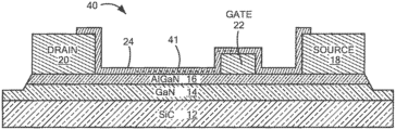
- a mesa structure 10 is shown having a substrate 12 , here for example, a semiconductor substrate such as gallium arsenide (GaAs), gallium nitride (GaN), silicon (Si), gallium oxide (Ga 2 O 3 ), or silicon carbide (SiC); a gallium nitride (GaN) buffer layer 14 on the substrate 12 and an aluminum gallium nitride (AlGaN) layer 16 on, and forming a heterojunction with, the GaN layer 14 .
- GaAs gallium arsenide
- GaN gallium nitride
- Si silicon
- Ga 2 O 3 gallium oxide
- SiC silicon carbide
- GaN gallium nitride
- AlGaN aluminum gallium nitride
- a source electrode 18 and a drain electrode 20 are in ohmic contact with the AlGaN layer 16 and a gate electrode 22 , disposed between the source electrode 18 and drain electrode 20 is here in Schottky contact with the AlGaN layer 16 , the gate electrode being used for controlling a flow of carriers between the source electrode 18 and the drain electrode 20 through a two-dimensional electron gas (2DEG) channel formed by the heterojunction.
- 2DEG two-dimensional electron gas
- a layer of dielectric material here silicon nitride (SiN x ), SiO 2 , Al 2 O 3 , or Ta 2 O 5 , for example, is formed over the surface of the structure by plasma enhanced chemical vapor deposition (PECVD), Low Pressure Chemical Vapor Deposition, for example, and patterned using conventional photolithography and etching processes to form a dielectric layer 24 over the surface as shown in FIG. 2 B .
- PECVD plasma enhanced chemical vapor deposition
- Low Pressure Chemical Vapor Deposition for example
- the layer 24 extends from a portion of the drain electrode 20 , over the surface of the AlGaN layer 16 between the drain electrode 20 and the gate electrode 22 , over the top and sides of the gate electrode 22 and then over the surface of the AlGaN layer 16 between the gate electrode 22 and the source electrode 18 and then over a portion of the source electrode 18 as shown. It should be noted that if the dielectric layer 24 is not of sufficient quality, a second dielectric layer 24 ′, can be deposited over the layer 24 for this purpose as will be described below in connection with FIG. 4 B ′.
- a mask 28 having a window 30 therein is disposed over the upper surface of the structures as shown.
- Ions 41 (here negative charge indicated by the symbol ( ⁇ ) from a source 29 external to the semiconductor structure 10 , here the source 29 is an ion implanter, are implanted via ion implantation into the portions of the dielectric layer 24 exposed by the window 30 .
- the distribution is uniform along the direction parallel to the surface of dielectric layer 24 and has a predetermined distribution in the depth of dielectric layer 24 ; here, for example, a Gaussian distribution having a peak at a predetermined depth into upper surface of dielectric layer 24 .
- ions are deposited into the region between drain and gate utilizing ion implantation of proper species (heavy ion to reduce diffusion in subsequent processing steps), charge (negative for n-channel transistors and positive for p-channel transistors, energy (low energy to create shallow layer in dielectric layer 24 ), and dose (sufficient dose to create the correct electrical potential of the self-biased field plate).
- This charge (ions) is deposited utilizing mask 28 , here a photolithographically defined mask, to restrict the region of implantation to the region between drain 20 and gate 22 without extending into the region between gate 22 and source 18 so as to eliminate any possible increase of the parasitic gate to source capacitance.
- the window 30 need not be merely a simple open window to deposit the charge uniformly into layer 24 , but may be modified to tailor the charge (ion) distribution and resultant semiconductor field such as a stipple of dots 30 ′ or stripes 30 ′′ as shown for masks 28 ′ and 28 ′′ in FIGS. 6 A and 6 B and FIGS. 7 A and 7 B , respectively to create a diffraction-like grating pattern to tailor the charge distribution and resultant semiconductor field.
- the apertures 30 ′ and 30 ′′ may be arranged in size and spacing to provide a graded charge distribution.
- the charge 41 is deposited non-uniformly into the dielectric layer 24 .
- the masks 28 ′ or 28 ′′ provide a predetermined, non-uniform, distribution of ions along the surface of the dielectric layers 24 or 24 ′.
- the correct ions to implant should be relatively large (slow thermal diffusion), such as negative ions Sr ⁇ , Ba ⁇ , Ra ⁇ , and Ca ⁇ , or positive ion of Cs + , and also be electrically stable to modify the semiconductor field over the expected device lifetime.
- the correct energy would be somewhat low to create a shallow, well defined sheet charge; for example, in a range of 10-40 keV.
- the correct dose would be determined through simulations and experiments and would depend on the masking method (rectangular or stippled); however, that dose would be on the order of 1e13 ions/cm 2 to 1e15 ions/cm 2 .
- the ions 41 are in place and the photolithographically defined mask 30 is removed, semiconductor processing is completed with the ion charge un-annealed and remaining in place to distribute the electric field in the gate to drain region.
- the electric field produced by the field plate structure 41 is provided solely by the electric ions 41 in the dielectric layer 24 .
- the process described above with regard to the ion implantation is not semiconductor doping, but rather charge implantation with the resulting implanted charge 41 creating an implanted dielectric field plate.
- the peak electric field at the drain side of the gate electrode is smaller than it would be if the device had been fabricated without the implanted ions. In this regard, the device is now capable of operating at higher voltages without its peak electric field exceeding an excessive or critical value.
- the Field Effect Transistor 40 structure shown in FIGS. 4 A and 4 B has a ground plane conductor 42 formed on the bottom of the substrate 12 .
- the source electrode 18 is connected to a ground plane conductor 42 through a conductive via 44 .
- the drain electrode 20 is connected to a positive voltage source +V through a resistor R and gate electrode 22 is connected to an RF input signal, as shown, to form a common source amplifier 48 . It is noted that here, the ion-implanted region extends over a portion of the gate electrode 22 towards the drain electrode 20 ; it being noted that the ion-implanted region does not extend all the way to the drain electrode 20 .
- the ion implanted region is localized only in a region between the gate and drain in this common source transistor example, to eliminate source electrode side capacitance increase.
- FIG. 4 B
Abstract
Description
-
-
Dielectric layer 24 thickness: 60 to 150 nm - Charge is implanted with a Gaussian-like distribution to a maximum depth: 30 to 50 nm in
layer 24 - The implanted charge peak depth: 5 to 20 nm into the upper surface of
layer 24
Double Dielectric StructureFIG. 4B ′: -
Dielectric layer 24′ thickness: 45 to 150 nm -
Dielectric layer 24 would be thinner thanlayer 24′ in the double dielectric configuration for device reasons other than the implanted field plate, such as device passivation - Charge is implanted with a Gaussian-like distribution layer to a maximum depth: 30 to 50 nm in
layer 24′ - The implanted charge peak depth: 5 to 20 nm into the upper surface of
layer 24′
-
Claims (7)
Priority Applications (9)
| Application Number | Priority Date | Filing Date | Title |
|---|---|---|---|
| US16/671,438 US11862691B2 (en) | 2019-11-01 | 2019-11-01 | Field effect transistor having field plate |
| JP2022525187A JP2023500261A (en) | 2019-11-01 | 2020-08-28 | field effect transistor with field plate |
| PCT/US2020/048323 WO2021086484A1 (en) | 2019-11-01 | 2020-08-28 | Field effect transistor having field plate |
| AU2020375557A AU2020375557A1 (en) | 2019-11-01 | 2020-08-28 | Field effect transistor having field plate |
| CN202080057609.6A CN114303247A (en) | 2019-11-01 | 2020-08-28 | Field effect transistor with field plate |
| EP20768801.1A EP4052301A1 (en) | 2019-11-01 | 2020-08-28 | Field effect transistor having field plate |
| KR1020227003546A KR20220029723A (en) | 2019-11-01 | 2020-08-28 | Field Effect Transistor with Field Plate |
| TW109131130A TWI765342B (en) | 2019-11-01 | 2020-09-10 | Field effect transistor having field plate |
| IL290252A IL290252A (en) | 2019-11-01 | 2022-01-31 | Field effect transistor having field plate |
Applications Claiming Priority (1)
| Application Number | Priority Date | Filing Date | Title |
|---|---|---|---|
| US16/671,438 US11862691B2 (en) | 2019-11-01 | 2019-11-01 | Field effect transistor having field plate |
Publications (2)
| Publication Number | Publication Date |
|---|---|
| US20210134965A1 US20210134965A1 (en) | 2021-05-06 |
| US11862691B2 true US11862691B2 (en) | 2024-01-02 |
Family
ID=72433056
Family Applications (1)
| Application Number | Title | Priority Date | Filing Date |
|---|---|---|---|
| US16/671,438 Active US11862691B2 (en) | 2019-11-01 | 2019-11-01 | Field effect transistor having field plate |
Country Status (9)
| Country | Link |
|---|---|
| US (1) | US11862691B2 (en) |
| EP (1) | EP4052301A1 (en) |
| JP (1) | JP2023500261A (en) |
| KR (1) | KR20220029723A (en) |
| CN (1) | CN114303247A (en) |
| AU (1) | AU2020375557A1 (en) |
| IL (1) | IL290252A (en) |
| TW (1) | TWI765342B (en) |
| WO (1) | WO2021086484A1 (en) |
Families Citing this family (1)
| Publication number | Priority date | Publication date | Assignee | Title |
|---|---|---|---|---|
| CN113410285B (en) * | 2021-08-04 | 2023-02-28 | 苏州汉骅半导体有限公司 | Semiconductor device and method for manufacturing the same |
Citations (17)
| Publication number | Priority date | Publication date | Assignee | Title |
|---|---|---|---|---|
| US6472722B1 (en) * | 2001-07-03 | 2002-10-29 | Industrial Technology Research Institute | Termination structure for high voltage devices |
| US20050274985A1 (en) | 2004-05-26 | 2005-12-15 | Adlerstein Michael G | RF decoupled field plate for FETs |
| US20060006415A1 (en) | 2004-05-11 | 2006-01-12 | Cree, Inc. | Wide bandgap HEMTs with source connected field plates |
| US20080073670A1 (en) * | 2006-09-22 | 2008-03-27 | Korea Advanced Institute Of Science And Technology | Gallium nitride high electron mobility transistor having inner field-plate for high power applications |
| US20100193866A1 (en) | 2009-01-30 | 2010-08-05 | G Robert Mulfinger | Graded well implantation for asymmetric transistors having reduced gate electrode pitches |
| US20100264486A1 (en) | 2009-04-20 | 2010-10-21 | Texas Instruments Incorporated | Field plate trench mosfet transistor with graded dielectric liner thickness |
| US20110221011A1 (en) * | 2007-02-22 | 2011-09-15 | Eldat Bahat-Treidel | Semiconductor component and method for producing the same |
| US8120064B2 (en) | 2003-09-09 | 2012-02-21 | Cree, Inc. | Wide bandgap transistor devices with field plates |
| US20120070970A1 (en) | 2010-09-17 | 2012-03-22 | Kabushiki Kaisha Toshiba | Method for manufacturing a semiconductor device |
| US8530978B1 (en) | 2011-12-06 | 2013-09-10 | Hrl Laboratories, Llc | High current high voltage GaN field effect transistors and method of fabricating same |
| US20140264360A1 (en) | 2013-03-14 | 2014-09-18 | Freescale Semiconductor, Inc., Austin, Texas | Transistor with charge enhanced field plate structure and method |
| US20140346615A1 (en) * | 2013-05-21 | 2014-11-27 | Massachusetts Institute Of Technology | Enhancement-mode transistors with increased threshold voltage |
| US20150115326A1 (en) * | 2013-10-31 | 2015-04-30 | Infineon Technologies Austria Ag | Electronic Device |
| US20150144953A1 (en) * | 2013-11-26 | 2015-05-28 | Darrell G. Hill | Transistors with field plates resistant to field plate material migration and methods of their fabrication |
| US9653556B1 (en) | 2016-02-29 | 2017-05-16 | Toshiba Corporation | Field plate for high-voltage field effect transistors |
| US20180175186A1 (en) * | 2016-12-20 | 2018-06-21 | Nuvoton Technology Corporation | Semiconductor substrate and semiconductor device |
| US20200219986A1 (en) * | 2019-01-08 | 2020-07-09 | Intel Corporation | Transistors with ion- or fixed charge-based field plate structures |
-
2019
- 2019-11-01 US US16/671,438 patent/US11862691B2/en active Active
-
2020
- 2020-08-28 WO PCT/US2020/048323 patent/WO2021086484A1/en active Application Filing
- 2020-08-28 JP JP2022525187A patent/JP2023500261A/en active Pending
- 2020-08-28 CN CN202080057609.6A patent/CN114303247A/en active Pending
- 2020-08-28 EP EP20768801.1A patent/EP4052301A1/en active Pending
- 2020-08-28 KR KR1020227003546A patent/KR20220029723A/en not_active Application Discontinuation
- 2020-08-28 AU AU2020375557A patent/AU2020375557A1/en active Pending
- 2020-09-10 TW TW109131130A patent/TWI765342B/en active
-
2022
- 2022-01-31 IL IL290252A patent/IL290252A/en unknown
Patent Citations (18)
| Publication number | Priority date | Publication date | Assignee | Title |
|---|---|---|---|---|
| US6472722B1 (en) * | 2001-07-03 | 2002-10-29 | Industrial Technology Research Institute | Termination structure for high voltage devices |
| US8120064B2 (en) | 2003-09-09 | 2012-02-21 | Cree, Inc. | Wide bandgap transistor devices with field plates |
| US20060006415A1 (en) | 2004-05-11 | 2006-01-12 | Cree, Inc. | Wide bandgap HEMTs with source connected field plates |
| US20050274985A1 (en) | 2004-05-26 | 2005-12-15 | Adlerstein Michael G | RF decoupled field plate for FETs |
| US20080073670A1 (en) * | 2006-09-22 | 2008-03-27 | Korea Advanced Institute Of Science And Technology | Gallium nitride high electron mobility transistor having inner field-plate for high power applications |
| US20110221011A1 (en) * | 2007-02-22 | 2011-09-15 | Eldat Bahat-Treidel | Semiconductor component and method for producing the same |
| US9449826B2 (en) | 2009-01-30 | 2016-09-20 | Advanced Micro Devices, Inc. | Graded well implantation for asymmetric transistors having reduced gate electrode pitches |
| US20100193866A1 (en) | 2009-01-30 | 2010-08-05 | G Robert Mulfinger | Graded well implantation for asymmetric transistors having reduced gate electrode pitches |
| US20100264486A1 (en) | 2009-04-20 | 2010-10-21 | Texas Instruments Incorporated | Field plate trench mosfet transistor with graded dielectric liner thickness |
| US20120070970A1 (en) | 2010-09-17 | 2012-03-22 | Kabushiki Kaisha Toshiba | Method for manufacturing a semiconductor device |
| US8530978B1 (en) | 2011-12-06 | 2013-09-10 | Hrl Laboratories, Llc | High current high voltage GaN field effect transistors and method of fabricating same |
| US20140264360A1 (en) | 2013-03-14 | 2014-09-18 | Freescale Semiconductor, Inc., Austin, Texas | Transistor with charge enhanced field plate structure and method |
| US20140346615A1 (en) * | 2013-05-21 | 2014-11-27 | Massachusetts Institute Of Technology | Enhancement-mode transistors with increased threshold voltage |
| US20150115326A1 (en) * | 2013-10-31 | 2015-04-30 | Infineon Technologies Austria Ag | Electronic Device |
| US20150144953A1 (en) * | 2013-11-26 | 2015-05-28 | Darrell G. Hill | Transistors with field plates resistant to field plate material migration and methods of their fabrication |
| US9653556B1 (en) | 2016-02-29 | 2017-05-16 | Toshiba Corporation | Field plate for high-voltage field effect transistors |
| US20180175186A1 (en) * | 2016-12-20 | 2018-06-21 | Nuvoton Technology Corporation | Semiconductor substrate and semiconductor device |
| US20200219986A1 (en) * | 2019-01-08 | 2020-07-09 | Intel Corporation | Transistors with ion- or fixed charge-based field plate structures |
Non-Patent Citations (7)
| Title |
|---|
| International Search Report dated Nov. 18, 2020 for International Application No. PCT/US2020/048323; 5 Pages. |
| Notification of Transmittal of the International Search Report and the Written Opinion of the ISA dated Nov. 18, 2020 for International Application No. PCT/US2020/048323; 1 Page. |
| PCT International Preliminary Report on Patentability dated May 12, 2022 for International Application No. PCT/US2020/048323; 10 Pages. |
| Response (with English Translation) to Taiwan Office Action dated Jun. 10, 2021 for Taiwan Application No. 109131130; Response filed Sep. 3, 2021; 43 Pages. |
| Taiwan Allowance Decision (with English Translation) dated Feb. 15, 2022 for Taiwan Application No. 109131130; 3 Pages. |
| Taiwanese Office Action with English Translation dated Jun. 10, 2021 for Taiwan Application No. 109131130; 17 Pages. |
| Written Opinion of the ISA dated Nov. 18, 2020 for International Application No. PCT/US2020/048323; 10 Pages. |
Also Published As
| Publication number | Publication date |
|---|---|
| JP2023500261A (en) | 2023-01-05 |
| AU2020375557A1 (en) | 2022-02-03 |
| TWI765342B (en) | 2022-05-21 |
| US20210134965A1 (en) | 2021-05-06 |
| IL290252A (en) | 2022-04-01 |
| CN114303247A (en) | 2022-04-08 |
| KR20220029723A (en) | 2022-03-08 |
| EP4052301A1 (en) | 2022-09-07 |
| WO2021086484A1 (en) | 2021-05-06 |
| TW202119638A (en) | 2021-05-16 |
Similar Documents
| Publication | Publication Date | Title |
|---|---|---|
| JP6726710B2 (en) | Oblique field plate power device and method for manufacturing oblique field plate power device | |
| US9419122B1 (en) | Etch-based fabrication process for stepped field-plate wide-bandgap | |
| KR20220076516A (en) | Stepped Field Plates Proximate Conduction Channel and Related Manufacturing Methods | |
| JP2009509343A (en) | N pole aluminum gallium nitride / gallium nitride enhancement mode field effect transistor | |
| EP2601678B1 (en) | Manufacturing of scalable gate length high electron mobility transistors | |
| US9000484B2 (en) | Non-uniform lateral profile of two-dimensional electron gas charge density in type III nitride HEMT devices using ion implantation through gray scale mask | |
| CN111048420B (en) | Method for manufacturing lateral double-diffused transistor | |
| TWI543368B (en) | Isolation structure in gallium nitride devices and integrated circuits | |
| US20220399460A1 (en) | Gan vertical trench mosfets and methods of manufacturing the same | |
| US11862691B2 (en) | Field effect transistor having field plate | |
| CN113178480A (en) | Enhanced HEMT radio frequency device with gate-drain composite stepped field plate structure and preparation method thereof | |
| US5877047A (en) | Lateral gate, vertical drift region transistor | |
| US20170278960A1 (en) | Semiconductor device and manufacturing method thereof | |
| EP3971991A1 (en) | Stacked gate mesfet/hemt transistor eliminating gate leakage current and providing normally off transistor | |
| TWI538208B (en) | Ion implanted and self aligned gate structure for gan transistors | |
| CN114649410A (en) | Trench type semiconductor device and method of manufacturing the same | |
| CN111668304A (en) | High-linearity MIS-HEMT device and preparation method thereof | |
| US20230223468A1 (en) | Multi-finger high-electron mobility transistor | |
| US20220059706A1 (en) | Single Sided Channel Mesa Power Junction Field Effect Transistor | |
| US20230215939A1 (en) | Semiconductor device and method for manufacturing the same | |
| JP2018037565A (en) | Method of manufacturing semiconductor device, and semiconductor device | |
| CN106876457B (en) | Groove gate enhanced MIS structure AlGaN/GaN heterojunction field effect transistor | |
| Perozek et al. | Vertical GaN Fin Transistors for Power and RF Applications | |
| CN117059660A (en) | GaN-based HEMT device and preparation method and application thereof | |
| JP2018037567A (en) | Method of manufacturing semiconductor device, and semiconductor device |
Legal Events
| Date | Code | Title | Description |
|---|---|---|---|
| AS | Assignment |
Owner name: RAYTHEON COMPANY, MASSACHUSETTS Free format text: ASSIGNMENT OF ASSIGNORS INTEREST;ASSIGNORS:DAVIS, MICHAEL S.;CHUMBES, EDUARDO M.;APPLETON, BRIAN T., JR.;REEL/FRAME:050890/0785 Effective date: 20191031 |
|
| FEPP | Fee payment procedure |
Free format text: ENTITY STATUS SET TO UNDISCOUNTED (ORIGINAL EVENT CODE: BIG.); ENTITY STATUS OF PATENT OWNER: LARGE ENTITY |
|
| STPP | Information on status: patent application and granting procedure in general |
Free format text: RESPONSE TO NON-FINAL OFFICE ACTION ENTERED AND FORWARDED TO EXAMINER |
|
| STPP | Information on status: patent application and granting procedure in general |
Free format text: FINAL REJECTION MAILED |
|
| STPP | Information on status: patent application and granting procedure in general |
Free format text: DOCKETED NEW CASE - READY FOR EXAMINATION |
|
| STPP | Information on status: patent application and granting procedure in general |
Free format text: NON FINAL ACTION MAILED |
|
| STPP | Information on status: patent application and granting procedure in general |
Free format text: FINAL REJECTION MAILED |
|
| STPP | Information on status: patent application and granting procedure in general |
Free format text: NON FINAL ACTION MAILED |
|
| STPP | Information on status: patent application and granting procedure in general |
Free format text: RESPONSE TO NON-FINAL OFFICE ACTION ENTERED AND FORWARDED TO EXAMINER |
|
| STPP | Information on status: patent application and granting procedure in general |
Free format text: NOTICE OF ALLOWANCE MAILED -- APPLICATION RECEIVED IN OFFICE OF PUBLICATIONS |
|
| STPP | Information on status: patent application and granting procedure in general |
Free format text: PUBLICATIONS -- ISSUE FEE PAYMENT RECEIVED |
|
| STPP | Information on status: patent application and granting procedure in general |
Free format text: PUBLICATIONS -- ISSUE FEE PAYMENT VERIFIED |
|
| STCF | Information on status: patent grant |
Free format text: PATENTED CASE |