JP6220161B2 - 半導体装置の製造方法 - Google Patents
半導体装置の製造方法 Download PDFInfo
- Publication number
- JP6220161B2 JP6220161B2 JP2013116659A JP2013116659A JP6220161B2 JP 6220161 B2 JP6220161 B2 JP 6220161B2 JP 2013116659 A JP2013116659 A JP 2013116659A JP 2013116659 A JP2013116659 A JP 2013116659A JP 6220161 B2 JP6220161 B2 JP 6220161B2
- Authority
- JP
- Japan
- Prior art keywords
- film
- insulating film
- semiconductor device
- layer
- trench
- Prior art date
- Legal status (The legal status is an assumption and is not a legal conclusion. Google has not performed a legal analysis and makes no representation as to the accuracy of the status listed.)
- Active
Links
Images


Classifications
-
- H—ELECTRICITY
- H10—SEMICONDUCTOR DEVICES; ELECTRIC SOLID-STATE DEVICES NOT OTHERWISE PROVIDED FOR
- H10D—INORGANIC ELECTRIC SEMICONDUCTOR DEVICES
- H10D30/00—Field-effect transistors [FET]
- H10D30/60—Insulated-gate field-effect transistors [IGFET]
- H10D30/63—Vertical IGFETs
- H10D30/635—Vertical IGFETs having no inversion channels, e.g. vertical accumulation channel FETs [ACCUFET] or normally-on vertical IGFETs
-
- H—ELECTRICITY
- H10—SEMICONDUCTOR DEVICES; ELECTRIC SOLID-STATE DEVICES NOT OTHERWISE PROVIDED FOR
- H10D—INORGANIC ELECTRIC SEMICONDUCTOR DEVICES
- H10D64/00—Electrodes of devices having potential barriers
- H10D64/01—Manufacture or treatment
- H10D64/013—Manufacture or treatment of electrodes having a conductor capacitively coupled to a semiconductor by an insulator
- H10D64/01358—Manufacture or treatment of electrodes having a conductor capacitively coupled to a semiconductor by an insulator the insulator being formed after the semiconductor body, the semiconductor being a Group III-V material
-
- H—ELECTRICITY
- H10—SEMICONDUCTOR DEVICES; ELECTRIC SOLID-STATE DEVICES NOT OTHERWISE PROVIDED FOR
- H10D—INORGANIC ELECTRIC SEMICONDUCTOR DEVICES
- H10D30/00—Field-effect transistors [FET]
- H10D30/01—Manufacture or treatment
- H10D30/015—Manufacture or treatment of FETs having heterojunction interface channels or heterojunction gate electrodes, e.g. HEMT
-
- H—ELECTRICITY
- H10—SEMICONDUCTOR DEVICES; ELECTRIC SOLID-STATE DEVICES NOT OTHERWISE PROVIDED FOR
- H10D—INORGANIC ELECTRIC SEMICONDUCTOR DEVICES
- H10D30/00—Field-effect transistors [FET]
- H10D30/40—FETs having zero-dimensional [0D], one-dimensional [1D] or two-dimensional [2D] charge carrier gas channels
- H10D30/47—FETs having zero-dimensional [0D], one-dimensional [1D] or two-dimensional [2D] charge carrier gas channels having two-dimensional [2D] charge carrier gas channels, e.g. nanoribbon FETs or high electron mobility transistors [HEMT]
- H10D30/471—High electron mobility transistors [HEMT] or high hole mobility transistors [HHMT]
- H10D30/473—High electron mobility transistors [HEMT] or high hole mobility transistors [HHMT] having confinement of carriers by multiple heterojunctions, e.g. quantum well HEMT
- H10D30/4732—High electron mobility transistors [HEMT] or high hole mobility transistors [HHMT] having confinement of carriers by multiple heterojunctions, e.g. quantum well HEMT using Group III-V semiconductor material
-
- H—ELECTRICITY
- H10—SEMICONDUCTOR DEVICES; ELECTRIC SOLID-STATE DEVICES NOT OTHERWISE PROVIDED FOR
- H10D—INORGANIC ELECTRIC SEMICONDUCTOR DEVICES
- H10D30/00—Field-effect transistors [FET]
- H10D30/40—FETs having zero-dimensional [0D], one-dimensional [1D] or two-dimensional [2D] charge carrier gas channels
- H10D30/47—FETs having zero-dimensional [0D], one-dimensional [1D] or two-dimensional [2D] charge carrier gas channels having two-dimensional [2D] charge carrier gas channels, e.g. nanoribbon FETs or high electron mobility transistors [HEMT]
- H10D30/471—High electron mobility transistors [HEMT] or high hole mobility transistors [HHMT]
- H10D30/475—High electron mobility transistors [HEMT] or high hole mobility transistors [HHMT] having wider bandgap layer formed on top of lower bandgap active layer, e.g. undoped barrier HEMTs such as i-AlGaN/GaN HEMTs
- H10D30/4755—High electron mobility transistors [HEMT] or high hole mobility transistors [HHMT] having wider bandgap layer formed on top of lower bandgap active layer, e.g. undoped barrier HEMTs such as i-AlGaN/GaN HEMTs having wide bandgap charge-carrier supplying layers, e.g. modulation doped HEMTs such as n-AlGaAs/GaAs HEMTs
-
- H—ELECTRICITY
- H10—SEMICONDUCTOR DEVICES; ELECTRIC SOLID-STATE DEVICES NOT OTHERWISE PROVIDED FOR
- H10D—INORGANIC ELECTRIC SEMICONDUCTOR DEVICES
- H10D30/00—Field-effect transistors [FET]
- H10D30/60—Insulated-gate field-effect transistors [IGFET]
- H10D30/63—Vertical IGFETs
-
- H—ELECTRICITY
- H10—SEMICONDUCTOR DEVICES; ELECTRIC SOLID-STATE DEVICES NOT OTHERWISE PROVIDED FOR
- H10D—INORGANIC ELECTRIC SEMICONDUCTOR DEVICES
- H10D30/00—Field-effect transistors [FET]
- H10D30/60—Insulated-gate field-effect transistors [IGFET]
- H10D30/64—Double-diffused metal-oxide semiconductor [DMOS] FETs
- H10D30/66—Vertical DMOS [VDMOS] FETs
- H10D30/667—Vertical DMOS [VDMOS] FETs having substrates comprising insulating layers, e.g. SOI-VDMOS transistors
-
- H—ELECTRICITY
- H10—SEMICONDUCTOR DEVICES; ELECTRIC SOLID-STATE DEVICES NOT OTHERWISE PROVIDED FOR
- H10D—INORGANIC ELECTRIC SEMICONDUCTOR DEVICES
- H10D30/00—Field-effect transistors [FET]
- H10D30/60—Insulated-gate field-effect transistors [IGFET]
- H10D30/64—Double-diffused metal-oxide semiconductor [DMOS] FETs
- H10D30/66—Vertical DMOS [VDMOS] FETs
- H10D30/668—Vertical DMOS [VDMOS] FETs having trench gate electrodes, e.g. UMOS transistors
-
- H—ELECTRICITY
- H10—SEMICONDUCTOR DEVICES; ELECTRIC SOLID-STATE DEVICES NOT OTHERWISE PROVIDED FOR
- H10D—INORGANIC ELECTRIC SEMICONDUCTOR DEVICES
- H10D64/00—Electrodes of devices having potential barriers
- H10D64/111—Field plates
-
- H—ELECTRICITY
- H10—SEMICONDUCTOR DEVICES; ELECTRIC SOLID-STATE DEVICES NOT OTHERWISE PROVIDED FOR
- H10D—INORGANIC ELECTRIC SEMICONDUCTOR DEVICES
- H10D64/00—Electrodes of devices having potential barriers
- H10D64/20—Electrodes characterised by their shapes, relative sizes or dispositions
- H10D64/27—Electrodes not carrying the current to be rectified, amplified, oscillated or switched, e.g. gates
- H10D64/311—Gate electrodes for field-effect devices
- H10D64/411—Gate electrodes for field-effect devices for FETs
- H10D64/511—Gate electrodes for field-effect devices for FETs for IGFETs
- H10D64/512—Disposition of the gate electrodes, e.g. buried gates
- H10D64/513—Disposition of the gate electrodes, e.g. buried gates within recesses in the substrate, e.g. trench gates, groove gates or buried gates
-
- H—ELECTRICITY
- H10—SEMICONDUCTOR DEVICES; ELECTRIC SOLID-STATE DEVICES NOT OTHERWISE PROVIDED FOR
- H10D—INORGANIC ELECTRIC SEMICONDUCTOR DEVICES
- H10D64/00—Electrodes of devices having potential barriers
- H10D64/20—Electrodes characterised by their shapes, relative sizes or dispositions
- H10D64/27—Electrodes not carrying the current to be rectified, amplified, oscillated or switched, e.g. gates
- H10D64/311—Gate electrodes for field-effect devices
- H10D64/411—Gate electrodes for field-effect devices for FETs
- H10D64/511—Gate electrodes for field-effect devices for FETs for IGFETs
- H10D64/514—Gate electrodes for field-effect devices for FETs for IGFETs characterised by the insulating layers
- H10D64/516—Gate electrodes for field-effect devices for FETs for IGFETs characterised by the insulating layers the thicknesses being non-uniform
-
- H—ELECTRICITY
- H10—SEMICONDUCTOR DEVICES; ELECTRIC SOLID-STATE DEVICES NOT OTHERWISE PROVIDED FOR
- H10D—INORGANIC ELECTRIC SEMICONDUCTOR DEVICES
- H10D64/00—Electrodes of devices having potential barriers
- H10D64/20—Electrodes characterised by their shapes, relative sizes or dispositions
- H10D64/27—Electrodes not carrying the current to be rectified, amplified, oscillated or switched, e.g. gates
- H10D64/311—Gate electrodes for field-effect devices
- H10D64/411—Gate electrodes for field-effect devices for FETs
- H10D64/511—Gate electrodes for field-effect devices for FETs for IGFETs
- H10D64/517—Gate electrodes for field-effect devices for FETs for IGFETs characterised by the conducting layers
- H10D64/518—Gate electrodes for field-effect devices for FETs for IGFETs characterised by the conducting layers characterised by their lengths or sectional shapes
-
- H—ELECTRICITY
- H10—SEMICONDUCTOR DEVICES; ELECTRIC SOLID-STATE DEVICES NOT OTHERWISE PROVIDED FOR
- H10D—INORGANIC ELECTRIC SEMICONDUCTOR DEVICES
- H10D64/00—Electrodes of devices having potential barriers
- H10D64/60—Electrodes characterised by their materials
- H10D64/66—Electrodes having a conductor capacitively coupled to a semiconductor by an insulator, e.g. MIS electrodes
- H10D64/68—Electrodes having a conductor capacitively coupled to a semiconductor by an insulator, e.g. MIS electrodes characterised by the insulator, e.g. by the gate insulator
- H10D64/681—Electrodes having a conductor capacitively coupled to a semiconductor by an insulator, e.g. MIS electrodes characterised by the insulator, e.g. by the gate insulator having a compositional variation, e.g. multilayered
- H10D64/685—Electrodes having a conductor capacitively coupled to a semiconductor by an insulator, e.g. MIS electrodes characterised by the insulator, e.g. by the gate insulator having a compositional variation, e.g. multilayered being perpendicular to the channel plane
-
- H—ELECTRICITY
- H10—SEMICONDUCTOR DEVICES; ELECTRIC SOLID-STATE DEVICES NOT OTHERWISE PROVIDED FOR
- H10P—GENERIC PROCESSES OR APPARATUS FOR THE MANUFACTURE OR TREATMENT OF DEVICES COVERED BY CLASS H10
- H10P14/00—Formation of materials, e.g. in the shape of layers or pillars
- H10P14/20—Formation of materials, e.g. in the shape of layers or pillars of semiconductor materials
- H10P14/24—Formation of materials, e.g. in the shape of layers or pillars of semiconductor materials using chemical vapour deposition [CVD]
-
- H—ELECTRICITY
- H10—SEMICONDUCTOR DEVICES; ELECTRIC SOLID-STATE DEVICES NOT OTHERWISE PROVIDED FOR
- H10P—GENERIC PROCESSES OR APPARATUS FOR THE MANUFACTURE OR TREATMENT OF DEVICES COVERED BY CLASS H10
- H10P14/00—Formation of materials, e.g. in the shape of layers or pillars
- H10P14/20—Formation of materials, e.g. in the shape of layers or pillars of semiconductor materials
- H10P14/34—Deposited materials, e.g. layers
- H10P14/3402—Deposited materials, e.g. layers characterised by the chemical composition
- H10P14/3414—Deposited materials, e.g. layers characterised by the chemical composition being group IIIA-VIA materials
- H10P14/3416—Nitrides
-
- H—ELECTRICITY
- H10—SEMICONDUCTOR DEVICES; ELECTRIC SOLID-STATE DEVICES NOT OTHERWISE PROVIDED FOR
- H10P—GENERIC PROCESSES OR APPARATUS FOR THE MANUFACTURE OR TREATMENT OF DEVICES COVERED BY CLASS H10
- H10P50/00—Etching of wafers, substrates or parts of devices
- H10P50/69—Etching of wafers, substrates or parts of devices using masks for semiconductor materials
- H10P50/691—Etching of wafers, substrates or parts of devices using masks for semiconductor materials for Group V materials or Group III-V materials
-
- H—ELECTRICITY
- H10—SEMICONDUCTOR DEVICES; ELECTRIC SOLID-STATE DEVICES NOT OTHERWISE PROVIDED FOR
- H10D—INORGANIC ELECTRIC SEMICONDUCTOR DEVICES
- H10D62/00—Semiconductor bodies, or regions thereof, of devices having potential barriers
- H10D62/80—Semiconductor bodies, or regions thereof, of devices having potential barriers characterised by the materials
- H10D62/85—Semiconductor bodies, or regions thereof, of devices having potential barriers characterised by the materials being Group III-V materials, e.g. GaAs
- H10D62/8503—Nitride Group III-V materials, e.g. AlN or GaN
-
- H—ELECTRICITY
- H10—SEMICONDUCTOR DEVICES; ELECTRIC SOLID-STATE DEVICES NOT OTHERWISE PROVIDED FOR
- H10D—INORGANIC ELECTRIC SEMICONDUCTOR DEVICES
- H10D64/00—Electrodes of devices having potential barriers
- H10D64/60—Electrodes characterised by their materials
- H10D64/62—Electrodes ohmically coupled to a semiconductor
Landscapes
- Insulated Gate Type Field-Effect Transistor (AREA)
- Junction Field-Effect Transistors (AREA)
- Chemical & Material Sciences (AREA)
- Engineering & Computer Science (AREA)
- Materials Engineering (AREA)
Description
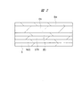
以下、図面を参照しながら本実施の形態の半導体装置について詳細に説明する。図1は、本実施の形態の半導体装置の構成を示す断面図である。図2〜図16は、本実施の形態の半導体装置の製造工程を示す断面図である。
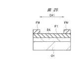
図1は、本実施の形態の半導体装置の構成を示す断面図である。図1に示す半導体装置は、窒化物半導体を用いたMIS(Metal Insulator Semiconductor)型の電界効果トランジスタ(FET;Field Effect Transistor)である。この半導体装置は、高電子移動度トランジスタ(HEMT:High Electron Mobility Transistor)やパワートランジスタとも呼ばれる。本実施の形態の半導体装置は、いわゆるリセスゲート型の半導体装置である。
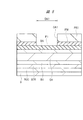
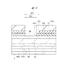
次いで、図2〜図16を参照しながら、本実施の形態の半導体装置の製造方法を説明するとともに、当該半導体装置の構成をより明確にする。図2〜図16は、本実施の形態の半導体装置の製造工程を示す断面図である。
上記実施の形態においては、絶縁膜IF1の溝T側の端部をドレイン電極DE側にのみ後退させたが、絶縁膜IF1の溝T側のドレイン電極DE側の端部およびソース電極SE側の端部のそれぞれを後退させてもよい。図19は、本実施の形態の半導体装置の変形例1の構成を模式的に示す断面図である。
上記実施の形態においては、溝Tの側壁を、障壁層BAやチャネル層CHの表面に対してほぼ垂直(テーパー角θ=90°)に形成したが、溝Tの側壁を、テーパー形状としてもよい。図20は、本実施の形態の半導体装置の変形例2の構成を模式的に示す断面図である。
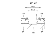
実施の形態1の変形例1においては、絶縁膜IF1の溝T側のドレイン電極DE側の端部およびソース電極SE側の端部のそれぞれを後退させ、また、変形例2においては、溝Tの側壁をテーパー形状としたが、絶縁膜IF1の溝T側のドレイン電極DE側の端部およびソース電極SE側の端部のそれぞれを後退させつつ、溝Tの側壁をテーパー形状としてもよい。図21は、本実施の形態の半導体装置の構成を模式的に示す断面図である。
図21に示すように、本実施の形態の半導体装置においては、絶縁膜IF1の溝T側のドレイン電極DE側の端部をドレイン電極DE側に後退量Ldだけ後退させ、さらに、絶縁膜IF1の溝T側のソース電極SE側の端部をソース電極SE側に後退量Lsだけ後退させている。そして、さらに、溝Tの側面(側壁)と溝Tの底面の延長面とのなす角度θが、90°未満となっている。他の構成は、実施の形態1と同様であるため、その説明を省略する。
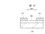
次いで、図22〜図30を参照しながら、本実施の形態の半導体装置の製造方法を説明するとともに、当該半導体装置の構成をより明確にする。図22〜図30は、本実施の形態の半導体装置の製造工程を示す断面図である。なお、実施の形態1と同様の工程については、その詳細な説明を省略する。
本実施の形態の半導体装置(図21)の諸特性(オン抵抗、S値、および電界強度)の評価結果について以下に説明する。なお、後退量Ld≒Lsとし、ゲート長(開口領域OA2の幅)は1μm、フィールドプレート電極の長さは2μm、ゲート電極GEとドレイン電極DEとの間の距離は10μmとした。
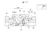
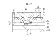
本実施の形態においては、チャネル部に不純物を含有する半導体領域を形成することにより、閾値Vthを向上させ、ノーマリーオフ特性をより安定化する例について説明する。図38は、本実施の形態の半導体装置の構成を模式的に示す断面図である。
図38に示すように、本実施の形態の半導体装置においては、溝Tの底面、即ち、チャネルが形成される領域に、不純物を含有する半導体領域DSが形成されている。なお、他の構成は、実施の形態2(図21)と同様であるため、その詳細な説明を省略する。即ち、本実施の形態の半導体装置においては、絶縁膜IF1の溝T側のドレイン電極DE側の端部をドレイン電極DE側に後退量Ldだけ後退させ、さらに、絶縁膜IF1の溝T側のソース電極SE側の端部をソース電極SE側に後退量Lsだけ後退させている。そして、さらに、溝Tの側面(側壁)と溝Tの底面の延長面とのなす角度が90°未満となっている。
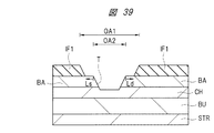
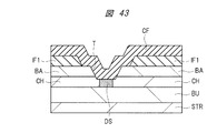
次いで、図39〜図45を参照しながら、本実施の形態の半導体装置の製造方法を説明するとともに、当該半導体装置の構成をより明確にする。図39〜図45は、本実施の形態の半導体装置の製造工程を示す断面図である。なお、実施の形態1や2と同様の工程については、その詳細な説明を省略する。
上記実施の形態1〜3で説明した半導体装置(トランジスタ)を適用する電子装置に制限は無いが、例えば、図46に示す電子装置に適用することができる。図46は、本実施の形態の電子装置の構成を示す回路図である。
22 電子装置
24 電源
26 負荷
210 トランジスタ
220 半導体装置
230 制御回路
BA 障壁層
BU バッファ層
C チャネル
C1 コンタクトホール
CF 被覆膜
CH チャネル層
DE ドレイン電極
DS 半導体領域
e 分極電荷
FP フィールドプレート電極
GE ゲート電極
GI ゲート絶縁膜
IF1 絶縁膜
IF2 絶縁膜
IFM 絶縁膜
IL1 絶縁層
IL2 絶縁層
Ld 後退量
Ls 後退量
NUC 核生成層
OA1 開口領域
OA2 開口領域
OA3 開口領域
P1 地点
P2 地点
PR1 フォトレジスト膜
PR2 フォトレジスト膜
PR3 フォトレジスト膜
S 基板
SE ソース電極
STR 歪緩和層
T 溝
T1 膜厚
T2 膜厚
Claims (3)
- (a)第1窒化物半導体層を形成し、前記第1窒化物半導体層上に、前記第1窒化物半導体層よりバンドギャップが広い第2窒化物半導体層を形成することにより積層体を形成する工程、
(b)前記積層体上の第1開口部を有する第1膜をマスクとして、前記積層体をエッチングすることにより、前記第2窒化物半導体層を貫通し、前記第1窒化物半導体層の途中まで到達する溝を形成する工程、
(c)前記第1膜の端部を前記溝の端部から後退させる工程、
(d)前記(c)工程の後、前記溝の内部を含む前記第1膜上に、第2膜を形成する工程、
(e)前記第2膜上に、ゲート電極を形成する工程、
を有し、
前記(b)工程は、
(b1)前記積層体上に、前記第1開口部を有する前記第1膜と、前記第1膜上に形成され、前記第1開口部の第1端から後退した第3膜との積層膜を形成する工程、
(b2)前記積層膜をマスクに、前記積層体をエッチングすることにより、前記溝を形成する工程、を有し、
前記(c)工程は、
(c1)前記第3膜をマスクに、前記第1膜をエッチングする工程、
(c2)前記第3膜を除去する工程、を有する、半導体装置の製造方法。 - 請求項1記載の半導体装置の製造方法において、
前記第1膜は、窒化シリコンを含有する膜であり、
前記第2膜は、酸化アルミニウムを含有する膜である、半導体装置の製造方法。 - 請求項1記載の半導体装置の製造方法において、
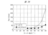
前記(c)工程は、前記第1膜の端部を前記溝の端部から0.2μm以上後退させる工程である、半導体装置の製造方法。
Priority Applications (9)
| Application Number | Priority Date | Filing Date | Title |
|---|---|---|---|
| JP2013116659A JP6220161B2 (ja) | 2013-06-03 | 2013-06-03 | 半導体装置の製造方法 |
| US14/271,277 US9559183B2 (en) | 2013-06-03 | 2014-05-06 | Semiconductor device with varying thickness of insulating film between electrode and gate electrode and method of manufacturing semiconductor device |
| TW107116193A TW201830707A (zh) | 2013-06-03 | 2014-05-19 | 半導體裝置之製造方法 |
| TW103117520A TWI627752B (zh) | 2013-06-03 | 2014-05-19 | 半導體裝置 |
| EP14169100.6A EP2811528A1 (en) | 2013-06-03 | 2014-05-20 | Semiconductor device and method of manufacturing a semiconductor device |
| KR1020140062770A KR102196786B1 (ko) | 2013-06-03 | 2014-05-26 | 반도체장치 및 반도체장치의 제조방법 |
| CN201410241729.8A CN104218079B (zh) | 2013-06-03 | 2014-06-03 | 半导体器件以及制造半导体器件的方法 |
| US15/385,507 US9984884B2 (en) | 2013-06-03 | 2016-12-20 | Method of manufacturing semiconductor device with a multi-layered gate dielectric |
| US15/882,687 US10410868B2 (en) | 2013-06-03 | 2018-01-29 | Semiconductor device and method of manufacturing semiconductor device |
Applications Claiming Priority (1)
| Application Number | Priority Date | Filing Date | Title |
|---|---|---|---|
| JP2013116659A JP6220161B2 (ja) | 2013-06-03 | 2013-06-03 | 半導体装置の製造方法 |
Related Child Applications (1)
| Application Number | Title | Priority Date | Filing Date |
|---|---|---|---|
| JP2017120266A Division JP6472839B2 (ja) | 2017-06-20 | 2017-06-20 | 半導体装置 |
Publications (3)
| Publication Number | Publication Date |
|---|---|
| JP2014236105A JP2014236105A (ja) | 2014-12-15 |
| JP2014236105A5 JP2014236105A5 (ja) | 2016-03-31 |
| JP6220161B2 true JP6220161B2 (ja) | 2017-10-25 |
Family
ID=50732057
Family Applications (1)
| Application Number | Title | Priority Date | Filing Date |
|---|---|---|---|
| JP2013116659A Active JP6220161B2 (ja) | 2013-06-03 | 2013-06-03 | 半導体装置の製造方法 |
Country Status (6)
| Country | Link |
|---|---|
| US (3) | US9559183B2 (ja) |
| EP (1) | EP2811528A1 (ja) |
| JP (1) | JP6220161B2 (ja) |
| KR (1) | KR102196786B1 (ja) |
| CN (1) | CN104218079B (ja) |
| TW (2) | TWI627752B (ja) |
Families Citing this family (48)
| Publication number | Priority date | Publication date | Assignee | Title |
|---|---|---|---|---|
| US7501669B2 (en) | 2003-09-09 | 2009-03-10 | Cree, Inc. | Wide bandgap transistor devices with field plates |
| US9773877B2 (en) | 2004-05-13 | 2017-09-26 | Cree, Inc. | Wide bandgap field effect transistors with source connected field plates |
| US11791385B2 (en) | 2005-03-11 | 2023-10-17 | Wolfspeed, Inc. | Wide bandgap transistors with gate-source field plates |
| US9443737B2 (en) | 2013-04-03 | 2016-09-13 | Texas Instruments Incorporated | Method of forming metal contacts in the barrier layer of a group III-N HEMT |
| US9679981B2 (en) * | 2013-06-09 | 2017-06-13 | Cree, Inc. | Cascode structures for GaN HEMTs |
| US9755059B2 (en) | 2013-06-09 | 2017-09-05 | Cree, Inc. | Cascode structures with GaN cap layers |
| US9847411B2 (en) * | 2013-06-09 | 2017-12-19 | Cree, Inc. | Recessed field plate transistor structures |
| JP2015177016A (ja) * | 2014-03-14 | 2015-10-05 | 株式会社東芝 | 半導体装置 |
| TWI567823B (zh) * | 2014-12-22 | 2017-01-21 | 群創光電股份有限公司 | 顯示面板與其製造方法 |
| JP6609926B2 (ja) * | 2015-01-21 | 2019-11-27 | 富士通株式会社 | 化合物半導体装置及びその製造方法 |
| JP6496149B2 (ja) * | 2015-01-22 | 2019-04-03 | ローム株式会社 | 半導体装置および半導体装置の製造方法 |
| US9954112B2 (en) | 2015-01-26 | 2018-04-24 | Semiconductor Energy Laboratory Co., Ltd. | Semiconductor device and manufacturing method thereof |
| JP6462393B2 (ja) * | 2015-02-10 | 2019-01-30 | ルネサスエレクトロニクス株式会社 | 半導体装置の製造方法および半導体装置 |
| JP6468886B2 (ja) | 2015-03-02 | 2019-02-13 | ルネサスエレクトロニクス株式会社 | 半導体装置の製造方法および半導体装置 |
| JP6659283B2 (ja) | 2015-09-14 | 2020-03-04 | 株式会社東芝 | 半導体装置 |
| JP6642883B2 (ja) * | 2015-10-08 | 2020-02-12 | ローム株式会社 | 窒化物半導体装置およびその製造方法 |
| ITUB20155536A1 (it) * | 2015-11-12 | 2017-05-12 | St Microelectronics Srl | Transistore hemt di tipo normalmente spento includente una trincea contenente una regione di gate e formante almeno un gradino, e relativo procedimento di fabbricazione |
| ITUB20155862A1 (it) * | 2015-11-24 | 2017-05-24 | St Microelectronics Srl | Transistore di tipo normalmente spento con ridotta resistenza in stato acceso e relativo metodo di fabbricazione |
| JP6560112B2 (ja) * | 2015-12-09 | 2019-08-14 | ルネサスエレクトロニクス株式会社 | 半導体装置およびその製造方法 |
| EP3252825B1 (en) | 2016-05-30 | 2022-12-21 | STMicroelectronics S.r.l. | Double-channel hemt device and manufacturing method thereof |
| US20170345921A1 (en) * | 2016-05-30 | 2017-11-30 | Epistar Corporation | Power device and method for fabricating thereof |
| TWI646228B (zh) | 2017-08-10 | 2019-01-01 | Nuvoton Technology Corporation | 半導體基板及其製造方法 |
| CN107331608B (zh) * | 2017-08-23 | 2020-11-24 | 成都海威华芯科技有限公司 | 一种双台阶t型栅的制作方法 |
| US11508824B2 (en) * | 2017-09-28 | 2022-11-22 | Intel Corporation | Gallium nitride transistors with multiple threshold voltages and their methods of fabrication |
| JP7308760B2 (ja) * | 2017-12-27 | 2023-07-14 | 株式会社半導体エネルギー研究所 | 半導体装置 |
| CN108447897A (zh) * | 2018-02-09 | 2018-08-24 | 沈阳工程学院 | 一种自支撑金刚石衬底异质结构及制备方法 |
| JP7316757B2 (ja) * | 2018-02-23 | 2023-07-28 | ローム株式会社 | 半導体装置 |
| JP6767411B2 (ja) * | 2018-03-06 | 2020-10-14 | 株式会社東芝 | 半導体装置、電源回路、及び、コンピュータ |
| JP6762977B2 (ja) * | 2018-03-06 | 2020-09-30 | 株式会社東芝 | 半導体装置、半導体装置の製造方法、電源回路、及び、コンピュータ |
| US11316038B2 (en) * | 2018-11-20 | 2022-04-26 | Stmicroelectronics S.R.L. | HEMT transistor with adjusted gate-source distance, and manufacturing method thereof |
| JP7367440B2 (ja) * | 2019-10-04 | 2023-10-24 | 住友電気工業株式会社 | 高電子移動度トランジスタの製造方法及び高電子移動度トランジスタ |
| EP3955314A1 (en) * | 2020-08-10 | 2022-02-16 | Infineon Technologies Austria AG | Group iii nitride device |
| JP7543773B2 (ja) * | 2020-08-25 | 2024-09-03 | 富士通株式会社 | 半導体装置及びその製造方法 |
| JP7470008B2 (ja) | 2020-10-19 | 2024-04-17 | 株式会社東芝 | 半導体装置 |
| US12349386B2 (en) | 2021-01-20 | 2025-07-01 | Kabushiki Kaisha Toshiba | Semiconductor device and method for manufacturing the same |
| US11682721B2 (en) * | 2021-01-20 | 2023-06-20 | Raytheon Company | Asymmetrically angled gate structure and method for making same |
| CN115458580B (zh) * | 2021-06-08 | 2025-12-09 | 株式会社东芝 | 半导体装置 |
| DE112022002854T5 (de) * | 2021-07-01 | 2024-03-14 | Rohm Co., Ltd. | Nitrid-halbleiterbauteil |
| US12218202B2 (en) * | 2021-09-16 | 2025-02-04 | Wolfspeed, Inc. | Semiconductor device incorporating a substrate recess |
| TWI776721B (zh) * | 2021-11-02 | 2022-09-01 | 國立陽明交通大學 | 功率半導體裝置的散熱方法 |
| WO2023082058A1 (en) * | 2021-11-09 | 2023-05-19 | Innoscience (Suzhou) Technology Co., Ltd. | Nitride-based semiconductor device and method for manufacturing thereof |
| US12477771B2 (en) * | 2022-03-25 | 2025-11-18 | Nuvoton Technology Corporation Japan | Semiconductor device |
| US12205825B2 (en) * | 2022-03-29 | 2025-01-21 | Nanya Technology Corporation | Method of preparing semiconductor structure having low dielectric constant layer |
| TWI819768B (zh) * | 2022-06-10 | 2023-10-21 | 強茂股份有限公司 | 金氧半導體元件及其製法 |
| JP7805321B2 (ja) * | 2023-01-17 | 2026-01-23 | 株式会社東芝 | 半導体装置 |
| CN116344612B (zh) * | 2023-05-24 | 2023-08-04 | 湖北九峰山实验室 | 垂直功率器件及其制作方法 |
| CN120882069A (zh) * | 2024-04-28 | 2025-10-31 | 华为技术有限公司 | 半导体工艺方法、半导体器件、电子设备 |
| US20260033382A1 (en) * | 2024-07-29 | 2026-01-29 | Texas Instruments Incorporated | Group iii-n device including surface passivation |
Family Cites Families (28)
| Publication number | Priority date | Publication date | Assignee | Title |
|---|---|---|---|---|
| JP4385205B2 (ja) * | 2002-12-16 | 2009-12-16 | 日本電気株式会社 | 電界効果トランジスタ |
| JP4417677B2 (ja) | 2003-09-19 | 2010-02-17 | 株式会社東芝 | 電力用半導体装置 |
| JP4888115B2 (ja) | 2004-02-20 | 2012-02-29 | 日本電気株式会社 | 電界効果トランジスタ |
| JPWO2005083104A1 (ja) | 2004-03-02 | 2008-01-17 | 三菱化学株式会社 | 無細胞タンパク質合成用細胞抽出液の製造法 |
| KR100636680B1 (ko) * | 2005-06-29 | 2006-10-23 | 주식회사 하이닉스반도체 | 리세스 게이트 및 비대칭 불순물영역을 갖는 반도체소자 및그 제조방법 |
| JP2007243080A (ja) * | 2006-03-13 | 2007-09-20 | Fuji Electric Holdings Co Ltd | 半導体装置およびその製造方法 |
| US7449762B1 (en) * | 2006-04-07 | 2008-11-11 | Wide Bandgap Llc | Lateral epitaxial GaN metal insulator semiconductor field effect transistor |
| JP2007311557A (ja) * | 2006-05-18 | 2007-11-29 | Toshiba Corp | 半導体装置及びその製造方法 |
| JP2008211172A (ja) * | 2007-01-31 | 2008-09-11 | Matsushita Electric Ind Co Ltd | 半導体装置および半導体装置の製造方法 |
| JP2008311269A (ja) * | 2007-06-12 | 2008-12-25 | Rohm Co Ltd | 窒化物半導体素子および窒化物半導体素子の製造方法 |
| US7859021B2 (en) * | 2007-08-29 | 2010-12-28 | Sanken Electric Co., Ltd. | Field-effect semiconductor device |
| JP4761319B2 (ja) * | 2008-02-19 | 2011-08-31 | シャープ株式会社 | 窒化物半導体装置とそれを含む電力変換装置 |
| JP2010118556A (ja) * | 2008-11-13 | 2010-05-27 | Furukawa Electric Co Ltd:The | 半導体装置および半導体装置の製造方法 |
| JP5653607B2 (ja) * | 2008-11-26 | 2015-01-14 | 古河電気工業株式会社 | GaN系電界効果トランジスタおよびその製造方法 |
| JP5564815B2 (ja) | 2009-03-31 | 2014-08-06 | サンケン電気株式会社 | 半導体装置及び半導体装置の製造方法 |
| JP4794656B2 (ja) * | 2009-06-11 | 2011-10-19 | シャープ株式会社 | 半導体装置 |
| JP2011044647A (ja) * | 2009-08-24 | 2011-03-03 | Sharp Corp | Iii族窒化物系電界効果トランジスタおよびその製造方法 |
| JP5589329B2 (ja) * | 2009-09-24 | 2014-09-17 | 豊田合成株式会社 | Iii族窒化物半導体からなる半導体装置、電力変換装置 |
| CN102343709B (zh) * | 2010-07-29 | 2015-09-30 | 海德堡印刷机械股份公司 | 用于在印刷机中对印刷页张撒布粉末的设备 |
| JP5694020B2 (ja) * | 2011-03-18 | 2015-04-01 | トランスフォーム・ジャパン株式会社 | トランジスタ回路 |
| JP5597581B2 (ja) * | 2011-03-23 | 2014-10-01 | 株式会社東芝 | 窒化物半導体装置及びその製造方法 |
| TWI544628B (zh) | 2011-05-16 | 2016-08-01 | 瑞薩電子股份有限公司 | Field effect transistor and semiconductor device |
| JP5548910B2 (ja) * | 2011-05-26 | 2014-07-16 | 古河電気工業株式会社 | 電界効果型トランジスタ |
| JP5825018B2 (ja) * | 2011-09-29 | 2015-12-02 | 富士通株式会社 | 化合物半導体装置及びその製造方法 |
| US8519767B2 (en) * | 2011-12-21 | 2013-08-27 | Micron Technology, Inc. | Methods, apparatuses, and circuits for bimodal disable circuits |
| KR20140013247A (ko) * | 2012-07-23 | 2014-02-05 | 삼성전자주식회사 | 질화물계 반도체 소자 및 그의 제조 방법 |
| JP6301640B2 (ja) * | 2013-11-28 | 2018-03-28 | ルネサスエレクトロニクス株式会社 | 半導体装置および半導体装置の製造方法 |
| JP6270572B2 (ja) * | 2014-03-19 | 2018-01-31 | 株式会社東芝 | 半導体装置及びその製造方法 |
-
2013
- 2013-06-03 JP JP2013116659A patent/JP6220161B2/ja active Active
-
2014
- 2014-05-06 US US14/271,277 patent/US9559183B2/en active Active
- 2014-05-19 TW TW103117520A patent/TWI627752B/zh active
- 2014-05-19 TW TW107116193A patent/TW201830707A/zh unknown
- 2014-05-20 EP EP14169100.6A patent/EP2811528A1/en not_active Withdrawn
- 2014-05-26 KR KR1020140062770A patent/KR102196786B1/ko active Active
- 2014-06-03 CN CN201410241729.8A patent/CN104218079B/zh active Active
-
2016
- 2016-12-20 US US15/385,507 patent/US9984884B2/en active Active
-
2018
- 2018-01-29 US US15/882,687 patent/US10410868B2/en active Active
Also Published As
| Publication number | Publication date |
|---|---|
| KR102196786B1 (ko) | 2020-12-30 |
| US10410868B2 (en) | 2019-09-10 |
| KR20140142147A (ko) | 2014-12-11 |
| US9559183B2 (en) | 2017-01-31 |
| US20180151377A1 (en) | 2018-05-31 |
| CN104218079A (zh) | 2014-12-17 |
| TW201830707A (zh) | 2018-08-16 |
| TW201448230A (zh) | 2014-12-16 |
| US20140353720A1 (en) | 2014-12-04 |
| CN104218079B (zh) | 2021-04-23 |
| EP2811528A1 (en) | 2014-12-10 |
| JP2014236105A (ja) | 2014-12-15 |
| US9984884B2 (en) | 2018-05-29 |
| US20170103898A1 (en) | 2017-04-13 |
| TWI627752B (zh) | 2018-06-21 |
Similar Documents
| Publication | Publication Date | Title |
|---|---|---|
| JP6220161B2 (ja) | 半導体装置の製造方法 | |
| US9853108B2 (en) | Nitride semiconductor device using insulating films having different bandgaps to enhance performance | |
| US10256100B2 (en) | Manufacturing method of semiconductor device and semiconductor device | |
| CN108604597B (zh) | 具有al(1-x)sixo栅极绝缘体的增强模式iii-氮化物器件 | |
| US9590071B2 (en) | Manufacturing method of semiconductor device and semiconductor device | |
| KR101527647B1 (ko) | 헤테로구조 반도체 디바이스 및 헤테로구조 반도체 디바이스의 제조 방법 | |
| CN104009075B (zh) | 半导体装置 | |
| CN106537560B (zh) | 形成增强模式iii族氮化物器件 | |
| JP6337726B2 (ja) | 半導体装置およびその製造方法 | |
| JP5688556B2 (ja) | 電界効果トランジスタ | |
| US20160225857A1 (en) | Semiconductor device and method for manufacturing the same | |
| US10784361B2 (en) | Semiconductor device and method for manufacturing the same | |
| KR20100138871A (ko) | 반도체 장치 및 반도체 장치의 제조 방법 | |
| JP6472839B2 (ja) | 半導体装置 | |
| CN103314438A (zh) | 氮化物系半导体装置 | |
| US8558242B2 (en) | Vertical GaN-based metal insulator semiconductor FET |
Legal Events
| Date | Code | Title | Description |
|---|---|---|---|
| A521 | Request for written amendment filed |
Free format text: JAPANESE INTERMEDIATE CODE: A523 Effective date: 20160215 |
|
| A621 | Written request for application examination |
Free format text: JAPANESE INTERMEDIATE CODE: A621 Effective date: 20160215 |
|
| A131 | Notification of reasons for refusal |
Free format text: JAPANESE INTERMEDIATE CODE: A131 Effective date: 20160913 |
|
| A521 | Request for written amendment filed |
Free format text: JAPANESE INTERMEDIATE CODE: A523 Effective date: 20161109 |
|
| A02 | Decision of refusal |
Free format text: JAPANESE INTERMEDIATE CODE: A02 Effective date: 20170321 |
|
| A521 | Request for written amendment filed |
Free format text: JAPANESE INTERMEDIATE CODE: A523 Effective date: 20170620 |
|
| A911 | Transfer to examiner for re-examination before appeal (zenchi) |
Free format text: JAPANESE INTERMEDIATE CODE: A911 Effective date: 20170628 |
|
| TRDD | Decision of grant or rejection written | ||
| A01 | Written decision to grant a patent or to grant a registration (utility model) |
Free format text: JAPANESE INTERMEDIATE CODE: A01 Effective date: 20170905 |
|
| A61 | First payment of annual fees (during grant procedure) |
Free format text: JAPANESE INTERMEDIATE CODE: A61 Effective date: 20170929 |
|
| R150 | Certificate of patent or registration of utility model |
Ref document number: 6220161 Country of ref document: JP Free format text: JAPANESE INTERMEDIATE CODE: R150 |