EP1563117B1 - Atomic layer deposition using metal amidinates - Google Patents
Atomic layer deposition using metal amidinates Download PDFInfo
- Publication number
- EP1563117B1 EP1563117B1 EP03783541A EP03783541A EP1563117B1 EP 1563117 B1 EP1563117 B1 EP 1563117B1 EP 03783541 A EP03783541 A EP 03783541A EP 03783541 A EP03783541 A EP 03783541A EP 1563117 B1 EP1563117 B1 EP 1563117B1
- Authority
- EP
- European Patent Office
- Prior art keywords
- groups
- metal
- amd
- cobalt
- matter
- Prior art date
- Legal status (The legal status is an assumption and is not a legal conclusion. Google has not performed a legal analysis and makes no representation as to the accuracy of the status listed.)
- Expired - Lifetime
Links
- 229910052751 metal Inorganic materials 0.000 title claims abstract description 108
- 239000002184 metal Substances 0.000 title claims abstract description 108
- 238000000231 atomic layer deposition Methods 0.000 title description 42
- 239000000758 substrate Substances 0.000 claims abstract description 78
- 229910052757 nitrogen Inorganic materials 0.000 claims abstract description 55
- 239000010949 copper Substances 0.000 claims abstract description 52
- 229910017052 cobalt Inorganic materials 0.000 claims abstract description 47
- 239000010941 cobalt Substances 0.000 claims abstract description 47
- GUTLYIVDDKVIGB-UHFFFAOYSA-N cobalt atom Chemical compound [Co] GUTLYIVDDKVIGB-UHFFFAOYSA-N 0.000 claims abstract description 44
- 229910052802 copper Inorganic materials 0.000 claims abstract description 41
- RYGMFSIKBFXOCR-UHFFFAOYSA-N Copper Chemical compound [Cu] RYGMFSIKBFXOCR-UHFFFAOYSA-N 0.000 claims abstract description 40
- UFHFLCQGNIYNRP-UHFFFAOYSA-N Hydrogen Chemical compound [H][H] UFHFLCQGNIYNRP-UHFFFAOYSA-N 0.000 claims abstract description 29
- XLYOFNOQVPJJNP-UHFFFAOYSA-N water Chemical compound O XLYOFNOQVPJJNP-UHFFFAOYSA-N 0.000 claims abstract description 29
- 239000001257 hydrogen Substances 0.000 claims abstract description 22
- 229910052739 hydrogen Inorganic materials 0.000 claims abstract description 22
- QGZKDVFQNNGYKY-UHFFFAOYSA-N Ammonia Chemical compound N QGZKDVFQNNGYKY-UHFFFAOYSA-N 0.000 claims abstract description 16
- 150000002739 metals Chemical class 0.000 claims abstract description 12
- VMQMZMRVKUZKQL-UHFFFAOYSA-N Cu+ Chemical compound [Cu+] VMQMZMRVKUZKQL-UHFFFAOYSA-N 0.000 claims abstract description 9
- 150000004767 nitrides Chemical class 0.000 claims abstract description 8
- 229910021529 ammonia Inorganic materials 0.000 claims abstract description 5
- XLJKHNWPARRRJB-UHFFFAOYSA-N cobalt(2+) Chemical compound [Co+2] XLJKHNWPARRRJB-UHFFFAOYSA-N 0.000 claims abstract description 5
- 238000000034 method Methods 0.000 claims description 67
- 230000008569 process Effects 0.000 claims description 41
- XEEYBQQBJWHFJM-UHFFFAOYSA-N Iron Chemical compound [Fe] XEEYBQQBJWHFJM-UHFFFAOYSA-N 0.000 claims description 35
- 150000001875 compounds Chemical class 0.000 claims description 28
- PXHVJJICTQNCMI-UHFFFAOYSA-N Nickel Chemical group [Ni] PXHVJJICTQNCMI-UHFFFAOYSA-N 0.000 claims description 25
- 239000000203 mixture Substances 0.000 claims description 24
- 238000000576 coating method Methods 0.000 claims description 23
- 125000000217 alkyl group Chemical group 0.000 claims description 22
- 239000007789 gas Substances 0.000 claims description 22
- 229910052742 iron Inorganic materials 0.000 claims description 15
- -1 lanthanide metals Chemical class 0.000 claims description 15
- 229910052746 lanthanum Inorganic materials 0.000 claims description 15
- FZLIPJUXYLNCLC-UHFFFAOYSA-N lanthanum atom Chemical group [La] FZLIPJUXYLNCLC-UHFFFAOYSA-N 0.000 claims description 14
- 239000007983 Tris buffer Substances 0.000 claims description 12
- 239000000539 dimer Substances 0.000 claims description 12
- 239000010936 titanium Chemical group 0.000 claims description 12
- 229910052759 nickel Inorganic materials 0.000 claims description 11
- 125000003709 fluoroalkyl group Chemical group 0.000 claims description 10
- 229910052707 ruthenium Inorganic materials 0.000 claims description 10
- KJTLSVCANCCWHF-UHFFFAOYSA-N Ruthenium Chemical group [Ru] KJTLSVCANCCWHF-UHFFFAOYSA-N 0.000 claims description 9
- RTAQQCXQSZGOHL-UHFFFAOYSA-N Titanium Chemical group [Ti] RTAQQCXQSZGOHL-UHFFFAOYSA-N 0.000 claims description 9
- 125000003342 alkenyl group Chemical group 0.000 claims description 9
- 125000000304 alkynyl group Chemical group 0.000 claims description 9
- 239000010409 thin film Substances 0.000 claims description 9
- 229910052719 titanium Inorganic materials 0.000 claims description 9
- 125000004665 trialkylsilyl group Chemical group 0.000 claims description 9
- 239000011248 coating agent Substances 0.000 claims description 8
- 239000011651 chromium Substances 0.000 claims description 6
- 229910044991 metal oxide Inorganic materials 0.000 claims description 6
- 150000004706 metal oxides Chemical class 0.000 claims description 6
- 125000002496 methyl group Chemical group [H]C([H])([H])* 0.000 claims description 6
- VYZAMTAEIAYCRO-UHFFFAOYSA-N Chromium Chemical compound [Cr] VYZAMTAEIAYCRO-UHFFFAOYSA-N 0.000 claims description 5
- QVGXLLKOCUKJST-UHFFFAOYSA-N atomic oxygen Chemical compound [O] QVGXLLKOCUKJST-UHFFFAOYSA-N 0.000 claims description 5
- 229910052804 chromium Inorganic materials 0.000 claims description 5
- 150000002431 hydrogen Chemical class 0.000 claims description 5
- WPBNNNQJVZRUHP-UHFFFAOYSA-L manganese(2+);methyl n-[[2-(methoxycarbonylcarbamothioylamino)phenyl]carbamothioyl]carbamate;n-[2-(sulfidocarbothioylamino)ethyl]carbamodithioate Chemical group [Mn+2].[S-]C(=S)NCCNC([S-])=S.COC(=O)NC(=S)NC1=CC=CC=C1NC(=S)NC(=O)OC WPBNNNQJVZRUHP-UHFFFAOYSA-L 0.000 claims description 5
- 239000010955 niobium Substances 0.000 claims description 5
- 229910052758 niobium Inorganic materials 0.000 claims description 5
- GUCVJGMIXFAOAE-UHFFFAOYSA-N niobium atom Chemical compound [Nb] GUCVJGMIXFAOAE-UHFFFAOYSA-N 0.000 claims description 5
- 239000001301 oxygen Substances 0.000 claims description 5
- 229910052760 oxygen Inorganic materials 0.000 claims description 5
- 239000000126 substance Substances 0.000 claims description 5
- 229910052715 tantalum Inorganic materials 0.000 claims description 5
- GUVRBAGPIYLISA-UHFFFAOYSA-N tantalum atom Chemical compound [Ta] GUVRBAGPIYLISA-UHFFFAOYSA-N 0.000 claims description 5
- 229910052777 Praseodymium Inorganic materials 0.000 claims description 4
- 229910052797 bismuth Inorganic materials 0.000 claims description 4
- JCXGWMGPZLAOME-UHFFFAOYSA-N bismuth atom Chemical compound [Bi] JCXGWMGPZLAOME-UHFFFAOYSA-N 0.000 claims description 4
- CZMAIROVPAYCMU-UHFFFAOYSA-N lanthanum(3+) Chemical compound [La+3] CZMAIROVPAYCMU-UHFFFAOYSA-N 0.000 claims description 4
- QJGQUHMNIGDVPM-UHFFFAOYSA-N nitrogen group Chemical group [N] QJGQUHMNIGDVPM-UHFFFAOYSA-N 0.000 claims description 4
- 229910052712 strontium Inorganic materials 0.000 claims description 4
- CIOAGBVUUVVLOB-UHFFFAOYSA-N strontium atom Chemical compound [Sr] CIOAGBVUUVVLOB-UHFFFAOYSA-N 0.000 claims description 4
- HCHKCACWOHOZIP-UHFFFAOYSA-N Zinc Chemical group [Zn] HCHKCACWOHOZIP-UHFFFAOYSA-N 0.000 claims description 3
- 125000000484 butyl group Chemical group [H]C([*])([H])C([H])([H])C([H])([H])C([H])([H])[H] 0.000 claims description 3
- 229910052741 iridium Inorganic materials 0.000 claims description 3
- GKOZUEZYRPOHIO-UHFFFAOYSA-N iridium atom Chemical compound [Ir] GKOZUEZYRPOHIO-UHFFFAOYSA-N 0.000 claims description 3
- 229910052747 lanthanoid Inorganic materials 0.000 claims description 3
- PUDIUYLPXJFUGB-UHFFFAOYSA-N praseodymium atom Chemical group [Pr] PUDIUYLPXJFUGB-UHFFFAOYSA-N 0.000 claims description 3
- 229910052706 scandium Inorganic materials 0.000 claims description 3
- SIXSYDAISGFNSX-UHFFFAOYSA-N scandium atom Chemical compound [Sc] SIXSYDAISGFNSX-UHFFFAOYSA-N 0.000 claims description 3
- 229910052709 silver Inorganic materials 0.000 claims description 3
- 239000004332 silver Substances 0.000 claims description 3
- 229910052727 yttrium Inorganic materials 0.000 claims description 3
- VWQVUPCCIRVNHF-UHFFFAOYSA-N yttrium atom Chemical compound [Y] VWQVUPCCIRVNHF-UHFFFAOYSA-N 0.000 claims description 3
- 229910052725 zinc Inorganic materials 0.000 claims description 3
- 239000011701 zinc Chemical group 0.000 claims description 3
- DGAQECJNVWCQMB-PUAWFVPOSA-M Ilexoside XXIX Chemical compound C[C@@H]1CC[C@@]2(CC[C@@]3(C(=CC[C@H]4[C@]3(CC[C@@H]5[C@@]4(CC[C@@H](C5(C)C)OS(=O)(=O)[O-])C)C)[C@@H]2[C@]1(C)O)C)C(=O)O[C@H]6[C@@H]([C@H]([C@@H]([C@H](O6)CO)O)O)O.[Na+] DGAQECJNVWCQMB-PUAWFVPOSA-M 0.000 claims description 2
- BQCADISMDOOEFD-UHFFFAOYSA-N Silver Chemical compound [Ag] BQCADISMDOOEFD-UHFFFAOYSA-N 0.000 claims description 2
- 229910052703 rhodium Inorganic materials 0.000 claims description 2
- 239000010948 rhodium Substances 0.000 claims description 2
- MHOVAHRLVXNVSD-UHFFFAOYSA-N rhodium atom Chemical compound [Rh] MHOVAHRLVXNVSD-UHFFFAOYSA-N 0.000 claims description 2
- 229910052708 sodium Inorganic materials 0.000 claims description 2
- 239000011734 sodium Substances 0.000 claims description 2
- OYPRJOBELJOOCE-UHFFFAOYSA-N Calcium Chemical group [Ca] OYPRJOBELJOOCE-UHFFFAOYSA-N 0.000 claims 2
- 229910052693 Europium Inorganic materials 0.000 claims 2
- 229910052791 calcium Chemical group 0.000 claims 2
- 239000011575 calcium Chemical group 0.000 claims 2
- OGPBJKLSAFTDLK-UHFFFAOYSA-N europium atom Chemical group [Eu] OGPBJKLSAFTDLK-UHFFFAOYSA-N 0.000 claims 2
- PCHJSUWPFVWCPO-UHFFFAOYSA-N gold Chemical compound [Au] PCHJSUWPFVWCPO-UHFFFAOYSA-N 0.000 claims 1
- 229910052737 gold Inorganic materials 0.000 claims 1
- 239000010931 gold Substances 0.000 claims 1
- 238000006243 chemical reaction Methods 0.000 abstract description 28
- 238000004377 microelectronic Methods 0.000 abstract description 6
- 238000003860 storage Methods 0.000 abstract description 2
- 239000002243 precursor Substances 0.000 description 64
- 238000000151 deposition Methods 0.000 description 43
- 230000008021 deposition Effects 0.000 description 37
- 239000000376 reactant Substances 0.000 description 31
- 239000010408 film Substances 0.000 description 25
- VLKZOEOYAKHREP-UHFFFAOYSA-N n-Hexane Chemical class CCCCCC VLKZOEOYAKHREP-UHFFFAOYSA-N 0.000 description 24
- 230000015572 biosynthetic process Effects 0.000 description 20
- MRELNEQAGSRDBK-UHFFFAOYSA-N lanthanum(3+);oxygen(2-) Chemical compound [O-2].[O-2].[O-2].[La+3].[La+3] MRELNEQAGSRDBK-UHFFFAOYSA-N 0.000 description 20
- 238000000859 sublimation Methods 0.000 description 20
- 230000008022 sublimation Effects 0.000 description 20
- 238000003786 synthesis reaction Methods 0.000 description 20
- RTZKZFJDLAIYFH-UHFFFAOYSA-N Diethyl ether Chemical compound CCOCC RTZKZFJDLAIYFH-UHFFFAOYSA-N 0.000 description 18
- WYURNTSHIVDZCO-UHFFFAOYSA-N Tetrahydrofuran Chemical compound C1CCOC1 WYURNTSHIVDZCO-UHFFFAOYSA-N 0.000 description 18
- 239000007787 solid Substances 0.000 description 17
- 239000000243 solution Substances 0.000 description 17
- 239000007788 liquid Substances 0.000 description 16
- VYPSYNLAJGMNEJ-UHFFFAOYSA-N Silicium dioxide Chemical compound O=[Si]=O VYPSYNLAJGMNEJ-UHFFFAOYSA-N 0.000 description 15
- 239000012159 carrier gas Substances 0.000 description 14
- UHOVQNZJYSORNB-MZWXYZOWSA-N benzene-d6 Chemical compound [2H]C1=C([2H])C([2H])=C([2H])C([2H])=C1[2H] UHOVQNZJYSORNB-MZWXYZOWSA-N 0.000 description 12
- 239000013078 crystal Substances 0.000 description 12
- 239000012691 Cu precursor Substances 0.000 description 10
- XUIMIQQOPSSXEZ-UHFFFAOYSA-N Silicon Chemical compound [Si] XUIMIQQOPSSXEZ-UHFFFAOYSA-N 0.000 description 10
- 150000001409 amidines Chemical class 0.000 description 10
- 125000004429 atom Chemical group 0.000 description 10
- 230000008901 benefit Effects 0.000 description 10
- 239000011572 manganese Substances 0.000 description 10
- 229910052710 silicon Inorganic materials 0.000 description 10
- 239000010703 silicon Substances 0.000 description 10
- 239000000047 product Substances 0.000 description 9
- YLQBMQCUIZJEEH-UHFFFAOYSA-N tetrahydrofuran Natural products C=1C=COC=1 YLQBMQCUIZJEEH-UHFFFAOYSA-N 0.000 description 9
- IJGRMHOSHXDMSA-UHFFFAOYSA-N Atomic nitrogen Chemical compound N#N IJGRMHOSHXDMSA-UHFFFAOYSA-N 0.000 description 8
- WHXSMMKQMYFTQS-UHFFFAOYSA-N Lithium Chemical compound [Li] WHXSMMKQMYFTQS-UHFFFAOYSA-N 0.000 description 8
- 239000003446 ligand Substances 0.000 description 8
- 229910052744 lithium Inorganic materials 0.000 description 8
- 238000005229 chemical vapour deposition Methods 0.000 description 7
- 238000001704 evaporation Methods 0.000 description 7
- 230000008020 evaporation Effects 0.000 description 7
- 239000000463 material Substances 0.000 description 7
- 238000005160 1H NMR spectroscopy Methods 0.000 description 6
- WEVYAHXRMPXWCK-UHFFFAOYSA-N Acetonitrile Chemical compound CC#N WEVYAHXRMPXWCK-UHFFFAOYSA-N 0.000 description 6
- UQSXHKLRYXJYBZ-UHFFFAOYSA-N Iron oxide Chemical compound [Fe]=O UQSXHKLRYXJYBZ-UHFFFAOYSA-N 0.000 description 6
- 230000008018 melting Effects 0.000 description 6
- 238000002844 melting Methods 0.000 description 6
- BASFCYQUMIYNBI-UHFFFAOYSA-N platinum Chemical compound [Pt] BASFCYQUMIYNBI-UHFFFAOYSA-N 0.000 description 6
- 239000000377 silicon dioxide Substances 0.000 description 6
- 239000002904 solvent Substances 0.000 description 6
- 238000006557 surface reaction Methods 0.000 description 6
- BDNKZNFMNDZQMI-UHFFFAOYSA-N 1,3-diisopropylcarbodiimide Chemical compound CC(C)N=C=NC(C)C BDNKZNFMNDZQMI-UHFFFAOYSA-N 0.000 description 5
- PWHULOQIROXLJO-UHFFFAOYSA-N Manganese Chemical compound [Mn] PWHULOQIROXLJO-UHFFFAOYSA-N 0.000 description 5
- 229910052748 manganese Inorganic materials 0.000 description 5
- IDVWLLCLTVBSCS-UHFFFAOYSA-N n,n'-ditert-butylmethanediimine Chemical compound CC(C)(C)N=C=NC(C)(C)C IDVWLLCLTVBSCS-UHFFFAOYSA-N 0.000 description 5
- 229910052755 nonmetal Inorganic materials 0.000 description 5
- 239000011541 reaction mixture Substances 0.000 description 5
- 239000013638 trimer Substances 0.000 description 5
- 238000009834 vaporization Methods 0.000 description 5
- 230000008016 vaporization Effects 0.000 description 5
- 229910021580 Cobalt(II) chloride Inorganic materials 0.000 description 4
- 239000012692 Fe precursor Substances 0.000 description 4
- KFZMGEQAYNKOFK-UHFFFAOYSA-N Isopropanol Chemical compound CC(C)O KFZMGEQAYNKOFK-UHFFFAOYSA-N 0.000 description 4
- 229910052782 aluminium Inorganic materials 0.000 description 4
- XAGFODPZIPBFFR-UHFFFAOYSA-N aluminium Chemical compound [Al] XAGFODPZIPBFFR-UHFFFAOYSA-N 0.000 description 4
- 230000004888 barrier function Effects 0.000 description 4
- WMWLMWRWZQELOS-UHFFFAOYSA-N bismuth(iii) oxide Chemical compound O=[Bi]O[Bi]=O WMWLMWRWZQELOS-UHFFFAOYSA-N 0.000 description 4
- 239000006227 byproduct Substances 0.000 description 4
- 150000001718 carbodiimides Chemical class 0.000 description 4
- 229910052799 carbon Inorganic materials 0.000 description 4
- 238000005137 deposition process Methods 0.000 description 4
- 238000004821 distillation Methods 0.000 description 4
- 238000005516 engineering process Methods 0.000 description 4
- 239000012705 liquid precursor Substances 0.000 description 4
- 239000011777 magnesium Substances 0.000 description 4
- CPLXHLVBOLITMK-UHFFFAOYSA-N magnesium oxide Inorganic materials [Mg]=O CPLXHLVBOLITMK-UHFFFAOYSA-N 0.000 description 4
- DVSDBMFJEQPWNO-UHFFFAOYSA-N methyllithium Chemical compound C[Li] DVSDBMFJEQPWNO-UHFFFAOYSA-N 0.000 description 4
- 239000000178 monomer Substances 0.000 description 4
- KTUFCUMIWABKDW-UHFFFAOYSA-N oxo(oxolanthaniooxy)lanthanum Chemical compound O=[La]O[La]=O KTUFCUMIWABKDW-UHFFFAOYSA-N 0.000 description 4
- 238000010992 reflux Methods 0.000 description 4
- 238000005001 rutherford backscattering spectroscopy Methods 0.000 description 4
- 235000012239 silicon dioxide Nutrition 0.000 description 4
- 239000011343 solid material Substances 0.000 description 4
- WJKHJLXJJJATHN-UHFFFAOYSA-N triflic anhydride Chemical compound FC(F)(F)S(=O)(=O)OS(=O)(=O)C(F)(F)F WJKHJLXJJJATHN-UHFFFAOYSA-N 0.000 description 4
- MONVAZUNBHXPRN-UHFFFAOYSA-N 3-methylpentanimidamide Chemical compound CCC(C)CC(N)=N MONVAZUNBHXPRN-UHFFFAOYSA-N 0.000 description 3
- GYHNNYVSQQEPJS-UHFFFAOYSA-N Gallium Chemical compound [Ga] GYHNNYVSQQEPJS-UHFFFAOYSA-N 0.000 description 3
- 229910002249 LaCl3 Inorganic materials 0.000 description 3
- FYYHWMGAXLPEAU-UHFFFAOYSA-N Magnesium Chemical compound [Mg] FYYHWMGAXLPEAU-UHFFFAOYSA-N 0.000 description 3
- HEMHJVSKTPXQMS-UHFFFAOYSA-M Sodium hydroxide Chemical compound [OH-].[Na+] HEMHJVSKTPXQMS-UHFFFAOYSA-M 0.000 description 3
- YXFVVABEGXRONW-UHFFFAOYSA-N Toluene Chemical compound CC1=CC=CC=C1 YXFVVABEGXRONW-UHFFFAOYSA-N 0.000 description 3
- 239000004411 aluminium Substances 0.000 description 3
- 150000001408 amides Chemical class 0.000 description 3
- 125000003118 aryl group Chemical group 0.000 description 3
- JHXKRIRFYBPWGE-UHFFFAOYSA-K bismuth chloride Chemical compound Cl[Bi](Cl)Cl JHXKRIRFYBPWGE-UHFFFAOYSA-K 0.000 description 3
- 125000004432 carbon atom Chemical group C* 0.000 description 3
- 229910000428 cobalt oxide Inorganic materials 0.000 description 3
- BKFAZDGHFACXKY-UHFFFAOYSA-N cobalt(II) bis(acetylacetonate) Chemical compound [Co+2].CC(=O)[CH-]C(C)=O.CC(=O)[CH-]C(C)=O BKFAZDGHFACXKY-UHFFFAOYSA-N 0.000 description 3
- IVMYJDGYRUAWML-UHFFFAOYSA-N cobalt(ii) oxide Chemical compound [Co]=O IVMYJDGYRUAWML-UHFFFAOYSA-N 0.000 description 3
- 230000007547 defect Effects 0.000 description 3
- 238000009792 diffusion process Methods 0.000 description 3
- 239000000706 filtrate Substances 0.000 description 3
- 229910052733 gallium Inorganic materials 0.000 description 3
- 229910052738 indium Inorganic materials 0.000 description 3
- APFVFJFRJDLVQX-UHFFFAOYSA-N indium atom Chemical compound [In] APFVFJFRJDLVQX-UHFFFAOYSA-N 0.000 description 3
- WGJJZRVGLPOKQT-UHFFFAOYSA-K lanthanum(3+);trifluoromethanesulfonate Chemical compound [La+3].[O-]S(=O)(=O)C(F)(F)F.[O-]S(=O)(=O)C(F)(F)F.[O-]S(=O)(=O)C(F)(F)F WGJJZRVGLPOKQT-UHFFFAOYSA-K 0.000 description 3
- ICAKDTKJOYSXGC-UHFFFAOYSA-K lanthanum(iii) chloride Chemical compound Cl[La](Cl)Cl ICAKDTKJOYSXGC-UHFFFAOYSA-K 0.000 description 3
- 229910052749 magnesium Inorganic materials 0.000 description 3
- 239000000395 magnesium oxide Substances 0.000 description 3
- 125000002524 organometallic group Chemical group 0.000 description 3
- TWNQGVIAIRXVLR-UHFFFAOYSA-N oxo(oxoalumanyloxy)alumane Chemical compound O=[Al]O[Al]=O TWNQGVIAIRXVLR-UHFFFAOYSA-N 0.000 description 3
- 229910052697 platinum Inorganic materials 0.000 description 3
- 238000010926 purge Methods 0.000 description 3
- 238000001878 scanning electron micrograph Methods 0.000 description 3
- 239000004065 semiconductor Substances 0.000 description 3
- 229910052721 tungsten Inorganic materials 0.000 description 3
- 239000010937 tungsten Substances 0.000 description 3
- XKRFYHLGVUSROY-UHFFFAOYSA-N Argon Chemical compound [Ar] XKRFYHLGVUSROY-UHFFFAOYSA-N 0.000 description 2
- 0 C*(*)(CC(CCC1*(**)CC(C2)C(*)C2(C*)CCC1)=*1*)C1=* Chemical compound C*(*)(CC(CCC1*(**)CC(C2)C(*)C2(C*)CCC1)=*1*)C1=* 0.000 description 2
- 239000005749 Copper compound Substances 0.000 description 2
- 229910021591 Copper(I) chloride Inorganic materials 0.000 description 2
- KRHYYFGTRYWZRS-UHFFFAOYSA-N Fluorane Chemical compound F KRHYYFGTRYWZRS-UHFFFAOYSA-N 0.000 description 2
- TWRXJAOTZQYOKJ-UHFFFAOYSA-L Magnesium chloride Chemical compound [Mg+2].[Cl-].[Cl-] TWRXJAOTZQYOKJ-UHFFFAOYSA-L 0.000 description 2
- 229910021380 Manganese Chloride Inorganic materials 0.000 description 2
- GLFNIEUTAYBVOC-UHFFFAOYSA-L Manganese chloride Chemical compound Cl[Mn]Cl GLFNIEUTAYBVOC-UHFFFAOYSA-L 0.000 description 2
- 229910021586 Nickel(II) chloride Inorganic materials 0.000 description 2
- URLKBWYHVLBVBO-UHFFFAOYSA-N Para-Xylene Chemical group CC1=CC=C(C)C=C1 URLKBWYHVLBVBO-UHFFFAOYSA-N 0.000 description 2
- JUJWROOIHBZHMG-UHFFFAOYSA-N Pyridine Chemical compound C1=CC=NC=C1 JUJWROOIHBZHMG-UHFFFAOYSA-N 0.000 description 2
- 229910010062 TiCl3 Inorganic materials 0.000 description 2
- 230000001464 adherent effect Effects 0.000 description 2
- 239000003570 air Substances 0.000 description 2
- PNEYBMLMFCGWSK-UHFFFAOYSA-N aluminium oxide Inorganic materials [O-2].[O-2].[O-2].[Al+3].[Al+3] PNEYBMLMFCGWSK-UHFFFAOYSA-N 0.000 description 2
- 125000000320 amidine group Chemical group 0.000 description 2
- 150000001412 amines Chemical class 0.000 description 2
- 239000012298 atmosphere Substances 0.000 description 2
- QVQLCTNNEUAWMS-UHFFFAOYSA-N barium oxide Chemical compound [Ba]=O QVQLCTNNEUAWMS-UHFFFAOYSA-N 0.000 description 2
- 229910000416 bismuth oxide Inorganic materials 0.000 description 2
- 150000001868 cobalt Chemical class 0.000 description 2
- 150000001869 cobalt compounds Chemical class 0.000 description 2
- GVPFVAHMJGGAJG-UHFFFAOYSA-L cobalt dichloride Chemical compound [Cl-].[Cl-].[Co+2] GVPFVAHMJGGAJG-UHFFFAOYSA-L 0.000 description 2
- 229910052681 coesite Inorganic materials 0.000 description 2
- 230000000052 comparative effect Effects 0.000 description 2
- 238000009833 condensation Methods 0.000 description 2
- 230000005494 condensation Effects 0.000 description 2
- 150000001880 copper compounds Chemical class 0.000 description 2
- OXBLHERUFWYNTN-UHFFFAOYSA-M copper(I) chloride Chemical compound [Cu]Cl OXBLHERUFWYNTN-UHFFFAOYSA-M 0.000 description 2
- 229910052593 corundum Inorganic materials 0.000 description 2
- 229910052906 cristobalite Inorganic materials 0.000 description 2
- 239000012043 crude product Substances 0.000 description 2
- DIOQZVSQGTUSAI-UHFFFAOYSA-N decane Chemical compound CCCCCCCCCC DIOQZVSQGTUSAI-UHFFFAOYSA-N 0.000 description 2
- 238000002716 delivery method Methods 0.000 description 2
- TYIXMATWDRGMPF-UHFFFAOYSA-N dibismuth;oxygen(2-) Chemical compound [O-2].[O-2].[O-2].[Bi+3].[Bi+3] TYIXMATWDRGMPF-UHFFFAOYSA-N 0.000 description 2
- 229910001873 dinitrogen Inorganic materials 0.000 description 2
- SNRUBQQJIBEYMU-UHFFFAOYSA-N dodecane Chemical compound CCCCCCCCCCCC SNRUBQQJIBEYMU-UHFFFAOYSA-N 0.000 description 2
- 230000006870 function Effects 0.000 description 2
- 239000005350 fused silica glass Substances 0.000 description 2
- 239000011521 glass Substances 0.000 description 2
- 239000003292 glue Substances 0.000 description 2
- AMWRITDGCCNYAT-UHFFFAOYSA-L hydroxy(oxo)manganese;manganese Chemical compound [Mn].O[Mn]=O.O[Mn]=O AMWRITDGCCNYAT-UHFFFAOYSA-L 0.000 description 2
- 150000007975 iminium salts Chemical class 0.000 description 2
- 125000001449 isopropyl group Chemical group [H]C([H])([H])C([H])(*)C([H])([H])[H] 0.000 description 2
- 150000002604 lanthanum compounds Chemical class 0.000 description 2
- AXZKOIWUVFPNLO-UHFFFAOYSA-N magnesium;oxygen(2-) Chemical compound [O-2].[Mg+2] AXZKOIWUVFPNLO-UHFFFAOYSA-N 0.000 description 2
- 239000011565 manganese chloride Substances 0.000 description 2
- VASIZKWUTCETSD-UHFFFAOYSA-N manganese(II) oxide Inorganic materials [Mn]=O VASIZKWUTCETSD-UHFFFAOYSA-N 0.000 description 2
- 238000004519 manufacturing process Methods 0.000 description 2
- 150000002736 metal compounds Chemical class 0.000 description 2
- 229910001507 metal halide Inorganic materials 0.000 description 2
- 150000005309 metal halides Chemical class 0.000 description 2
- 238000002663 nebulization Methods 0.000 description 2
- QMMRZOWCJAIUJA-UHFFFAOYSA-L nickel dichloride Chemical compound Cl[Ni]Cl QMMRZOWCJAIUJA-UHFFFAOYSA-L 0.000 description 2
- 239000003921 oil Substances 0.000 description 2
- 239000012071 phase Substances 0.000 description 2
- 238000000746 purification Methods 0.000 description 2
- 238000005070 sampling Methods 0.000 description 2
- BHRZNVHARXXAHW-UHFFFAOYSA-N sec-butylamine Chemical compound CCC(C)N BHRZNVHARXXAHW-UHFFFAOYSA-N 0.000 description 2
- 125000005353 silylalkyl group Chemical group 0.000 description 2
- 229910052682 stishovite Inorganic materials 0.000 description 2
- BGHCVCJVXZWKCC-UHFFFAOYSA-N tetradecane Chemical compound CCCCCCCCCCCCCC BGHCVCJVXZWKCC-UHFFFAOYSA-N 0.000 description 2
- YONPGGFAJWQGJC-UHFFFAOYSA-K titanium(iii) chloride Chemical compound Cl[Ti](Cl)Cl YONPGGFAJWQGJC-UHFFFAOYSA-K 0.000 description 2
- 229910052905 tridymite Inorganic materials 0.000 description 2
- JLTRXTDYQLMHGR-UHFFFAOYSA-N trimethylaluminium Chemical compound C[Al](C)C JLTRXTDYQLMHGR-UHFFFAOYSA-N 0.000 description 2
- 238000007740 vapor deposition Methods 0.000 description 2
- 239000003039 volatile agent Substances 0.000 description 2
- 229910001845 yogo sapphire Inorganic materials 0.000 description 2
- OKTJSMMVPCPJKN-UHFFFAOYSA-N Carbon Chemical compound [C] OKTJSMMVPCPJKN-UHFFFAOYSA-N 0.000 description 1
- 241000283153 Cetacea Species 0.000 description 1
- VEXZGXHMUGYJMC-UHFFFAOYSA-M Chloride anion Chemical compound [Cl-] VEXZGXHMUGYJMC-UHFFFAOYSA-M 0.000 description 1
- 229910020676 Co—N Inorganic materials 0.000 description 1
- JPVYNHNXODAKFH-UHFFFAOYSA-N Cu2+ Chemical compound [Cu+2] JPVYNHNXODAKFH-UHFFFAOYSA-N 0.000 description 1
- 229910021577 Iron(II) chloride Inorganic materials 0.000 description 1
- 229910002244 LaAlO3 Inorganic materials 0.000 description 1
- 101100007427 Manduca sexta COVA gene Proteins 0.000 description 1
- 229910014291 N—Cu Inorganic materials 0.000 description 1
- CTQNGGLPUBDAKN-UHFFFAOYSA-N O-Xylene Chemical compound CC1=CC=CC=C1C CTQNGGLPUBDAKN-UHFFFAOYSA-N 0.000 description 1
- 229910019891 RuCl3 Inorganic materials 0.000 description 1
- 238000004639 Schlenk technique Methods 0.000 description 1
- BLRPTPMANUNPDV-UHFFFAOYSA-N Silane Chemical compound [SiH4] BLRPTPMANUNPDV-UHFFFAOYSA-N 0.000 description 1
- 229910021607 Silver chloride Inorganic materials 0.000 description 1
- FOIXSVOLVBLSDH-UHFFFAOYSA-N Silver ion Chemical compound [Ag+] FOIXSVOLVBLSDH-UHFFFAOYSA-N 0.000 description 1
- ATJFFYVFTNAWJD-UHFFFAOYSA-N Tin Chemical compound [Sn] ATJFFYVFTNAWJD-UHFFFAOYSA-N 0.000 description 1
- 229910021551 Vanadium(III) chloride Inorganic materials 0.000 description 1
- CGMZMFSAWXBLKD-UHFFFAOYSA-N [In].[Ir] Chemical compound [In].[Ir] CGMZMFSAWXBLKD-UHFFFAOYSA-N 0.000 description 1
- JAZCEXBNIYKZDI-UHFFFAOYSA-N [Ir+] Chemical compound [Ir+] JAZCEXBNIYKZDI-UHFFFAOYSA-N 0.000 description 1
- 239000002390 adhesive tape Substances 0.000 description 1
- 229910052783 alkali metal Inorganic materials 0.000 description 1
- 150000003973 alkyl amines Chemical class 0.000 description 1
- 125000005210 alkyl ammonium group Chemical group 0.000 description 1
- 239000012080 ambient air Substances 0.000 description 1
- 229910052786 argon Inorganic materials 0.000 description 1
- 238000003877 atomic layer epitaxy Methods 0.000 description 1
- QCLQZCOGUCNIOC-UHFFFAOYSA-N azanylidynelanthanum Chemical compound [La]#N QCLQZCOGUCNIOC-UHFFFAOYSA-N 0.000 description 1
- IVHJCRXBQPGLOV-UHFFFAOYSA-N azanylidynetungsten Chemical compound [W]#N IVHJCRXBQPGLOV-UHFFFAOYSA-N 0.000 description 1
- 239000002585 base Substances 0.000 description 1
- 150000003937 benzamidines Chemical class 0.000 description 1
- ODWXUNBKCRECNW-UHFFFAOYSA-M bromocopper(1+) Chemical compound Br[Cu+] ODWXUNBKCRECNW-UHFFFAOYSA-M 0.000 description 1
- KPVUHKHVGKSEPB-UHFFFAOYSA-N calcium europium Chemical compound [Ca][Eu] KPVUHKHVGKSEPB-UHFFFAOYSA-N 0.000 description 1
- 239000003990 capacitor Substances 0.000 description 1
- 239000003054 catalyst Substances 0.000 description 1
- 239000003638 chemical reducing agent Substances 0.000 description 1
- 150000008280 chlorinated hydrocarbons Chemical class 0.000 description 1
- UZEDIBTVIIJELN-UHFFFAOYSA-N chromium(2+) Chemical compound [Cr+2] UZEDIBTVIIJELN-UHFFFAOYSA-N 0.000 description 1
- 238000004140 cleaning Methods 0.000 description 1
- 238000010960 commercial process Methods 0.000 description 1
- 238000007796 conventional method Methods 0.000 description 1
- 238000001816 cooling Methods 0.000 description 1
- 239000008367 deionised water Substances 0.000 description 1
- 229910021641 deionized water Inorganic materials 0.000 description 1
- 230000001934 delay Effects 0.000 description 1
- 238000001035 drying Methods 0.000 description 1
- 230000000694 effects Effects 0.000 description 1
- 238000001803 electron scattering Methods 0.000 description 1
- 150000002148 esters Chemical class 0.000 description 1
- 150000002170 ethers Chemical class 0.000 description 1
- 230000007717 exclusion Effects 0.000 description 1
- 238000000605 extraction Methods 0.000 description 1
- 238000001914 filtration Methods 0.000 description 1
- 238000004508 fractional distillation Methods 0.000 description 1
- 238000004817 gas chromatography Methods 0.000 description 1
- 229910021397 glassy carbon Inorganic materials 0.000 description 1
- ZBKIUFWVEIBQRT-UHFFFAOYSA-N gold(1+) Chemical compound [Au+] ZBKIUFWVEIBQRT-UHFFFAOYSA-N 0.000 description 1
- 229910052736 halogen Inorganic materials 0.000 description 1
- 150000002367 halogens Chemical class 0.000 description 1
- 238000010438 heat treatment Methods 0.000 description 1
- 229930195733 hydrocarbon Natural products 0.000 description 1
- 150000002430 hydrocarbons Chemical class 0.000 description 1
- 230000006872 improvement Effects 0.000 description 1
- 239000012535 impurity Substances 0.000 description 1
- 230000000977 initiatory effect Effects 0.000 description 1
- 238000002347 injection Methods 0.000 description 1
- 239000007924 injection Substances 0.000 description 1
- NMCUIPGRVMDVDB-UHFFFAOYSA-L iron dichloride Chemical compound Cl[Fe]Cl NMCUIPGRVMDVDB-UHFFFAOYSA-L 0.000 description 1
- 150000002576 ketones Chemical class 0.000 description 1
- UBJFKNSINUCEAL-UHFFFAOYSA-N lithium;2-methylpropane Chemical compound [Li+].C[C-](C)C UBJFKNSINUCEAL-UHFFFAOYSA-N 0.000 description 1
- 238000010550 living polymerization reaction Methods 0.000 description 1
- 229920002521 macromolecule Polymers 0.000 description 1
- 229910001629 magnesium chloride Inorganic materials 0.000 description 1
- PPNAOCWZXJOHFK-UHFFFAOYSA-N manganese(2+);oxygen(2-) Chemical compound [O-2].[Mn+2] PPNAOCWZXJOHFK-UHFFFAOYSA-N 0.000 description 1
- QSHDDOUJBYECFT-UHFFFAOYSA-N mercury Chemical compound [Hg] QSHDDOUJBYECFT-UHFFFAOYSA-N 0.000 description 1
- 229910052753 mercury Inorganic materials 0.000 description 1
- AUHZEENZYGFFBQ-UHFFFAOYSA-N mesitylene Substances CC1=CC(C)=CC(C)=C1 AUHZEENZYGFFBQ-UHFFFAOYSA-N 0.000 description 1
- 125000001827 mesitylenyl group Chemical group [H]C1=C(C(*)=C(C([H])=C1C([H])([H])[H])C([H])([H])[H])C([H])([H])[H] 0.000 description 1
- 229910052987 metal hydride Inorganic materials 0.000 description 1
- 150000004681 metal hydrides Chemical class 0.000 description 1
- 238000001000 micrograph Methods 0.000 description 1
- 238000013508 migration Methods 0.000 description 1
- 238000002156 mixing Methods 0.000 description 1
- 239000002808 molecular sieve Substances 0.000 description 1
- 150000002825 nitriles Chemical class 0.000 description 1
- 239000012299 nitrogen atmosphere Substances 0.000 description 1
- 229910000069 nitrogen hydride Inorganic materials 0.000 description 1
- 238000000879 optical micrograph Methods 0.000 description 1
- 238000000399 optical microscopy Methods 0.000 description 1
- 150000007524 organic acids Chemical class 0.000 description 1
- 150000007530 organic bases Chemical class 0.000 description 1
- 239000003960 organic solvent Substances 0.000 description 1
- 239000000843 powder Substances 0.000 description 1
- 239000002244 precipitate Substances 0.000 description 1
- 238000002360 preparation method Methods 0.000 description 1
- UMJSCPRVCHMLSP-UHFFFAOYSA-N pyridine Natural products COC1=CC=CN=C1 UMJSCPRVCHMLSP-UHFFFAOYSA-N 0.000 description 1
- 238000001953 recrystallisation Methods 0.000 description 1
- 238000012552 review Methods 0.000 description 1
- YBCAZPLXEGKKFM-UHFFFAOYSA-K ruthenium(iii) chloride Chemical compound [Cl-].[Cl-].[Cl-].[Ru+3] YBCAZPLXEGKKFM-UHFFFAOYSA-K 0.000 description 1
- 150000003839 salts Chemical class 0.000 description 1
- 125000002914 sec-butyl group Chemical group [H]C([H])([H])C([H])([H])C([H])(*)C([H])([H])[H] 0.000 description 1
- 229910000077 silane Inorganic materials 0.000 description 1
- HKZLPVFGJNLROG-UHFFFAOYSA-M silver monochloride Chemical compound [Cl-].[Ag+] HKZLPVFGJNLROG-UHFFFAOYSA-M 0.000 description 1
- URGAHOPLAPQHLN-UHFFFAOYSA-N sodium aluminosilicate Chemical compound [Na+].[Al+3].[O-][Si]([O-])=O.[O-][Si]([O-])=O URGAHOPLAPQHLN-UHFFFAOYSA-N 0.000 description 1
- 229910001220 stainless steel Inorganic materials 0.000 description 1
- 239000010935 stainless steel Substances 0.000 description 1
- 230000003068 static effect Effects 0.000 description 1
- 229910001631 strontium chloride Inorganic materials 0.000 description 1
- AHBGXTDRMVNFER-UHFFFAOYSA-L strontium dichloride Chemical compound [Cl-].[Cl-].[Sr+2] AHBGXTDRMVNFER-UHFFFAOYSA-L 0.000 description 1
- 125000000999 tert-butyl group Chemical group [H]C([H])([H])C(*)(C([H])([H])[H])C([H])([H])[H] 0.000 description 1
- 238000005979 thermal decomposition reaction Methods 0.000 description 1
- 238000012546 transfer Methods 0.000 description 1
- 229910052723 transition metal Inorganic materials 0.000 description 1
- 150000003624 transition metals Chemical class 0.000 description 1
- ITMCEJHCFYSIIV-UHFFFAOYSA-M triflate Chemical compound [O-]S(=O)(=O)C(F)(F)F ITMCEJHCFYSIIV-UHFFFAOYSA-M 0.000 description 1
- 229910052720 vanadium Inorganic materials 0.000 description 1
- GPPXJZIENCGNKB-UHFFFAOYSA-N vanadium Chemical compound [V]#[V] GPPXJZIENCGNKB-UHFFFAOYSA-N 0.000 description 1
- HQYCOEXWFMFWLR-UHFFFAOYSA-K vanadium(iii) chloride Chemical compound [Cl-].[Cl-].[Cl-].[V+3] HQYCOEXWFMFWLR-UHFFFAOYSA-K 0.000 description 1
- 239000012808 vapor phase Substances 0.000 description 1
- 238000002424 x-ray crystallography Methods 0.000 description 1
- 239000008096 xylene Substances 0.000 description 1
Images

Classifications
-
- C—CHEMISTRY; METALLURGY
- C23—COATING METALLIC MATERIAL; COATING MATERIAL WITH METALLIC MATERIAL; CHEMICAL SURFACE TREATMENT; DIFFUSION TREATMENT OF METALLIC MATERIAL; COATING BY VACUUM EVAPORATION, BY SPUTTERING, BY ION IMPLANTATION OR BY CHEMICAL VAPOUR DEPOSITION, IN GENERAL; INHIBITING CORROSION OF METALLIC MATERIAL OR INCRUSTATION IN GENERAL
- C23C—COATING METALLIC MATERIAL; COATING MATERIAL WITH METALLIC MATERIAL; SURFACE TREATMENT OF METALLIC MATERIAL BY DIFFUSION INTO THE SURFACE, BY CHEMICAL CONVERSION OR SUBSTITUTION; COATING BY VACUUM EVAPORATION, BY SPUTTERING, BY ION IMPLANTATION OR BY CHEMICAL VAPOUR DEPOSITION, IN GENERAL
- C23C16/00—Chemical coating by decomposition of gaseous compounds, without leaving reaction products of surface material in the coating, i.e. chemical vapour deposition [CVD] processes
- C23C16/06—Chemical coating by decomposition of gaseous compounds, without leaving reaction products of surface material in the coating, i.e. chemical vapour deposition [CVD] processes characterised by the deposition of metallic material
-
- C—CHEMISTRY; METALLURGY
- C23—COATING METALLIC MATERIAL; COATING MATERIAL WITH METALLIC MATERIAL; CHEMICAL SURFACE TREATMENT; DIFFUSION TREATMENT OF METALLIC MATERIAL; COATING BY VACUUM EVAPORATION, BY SPUTTERING, BY ION IMPLANTATION OR BY CHEMICAL VAPOUR DEPOSITION, IN GENERAL; INHIBITING CORROSION OF METALLIC MATERIAL OR INCRUSTATION IN GENERAL
- C23C—COATING METALLIC MATERIAL; COATING MATERIAL WITH METALLIC MATERIAL; SURFACE TREATMENT OF METALLIC MATERIAL BY DIFFUSION INTO THE SURFACE, BY CHEMICAL CONVERSION OR SUBSTITUTION; COATING BY VACUUM EVAPORATION, BY SPUTTERING, BY ION IMPLANTATION OR BY CHEMICAL VAPOUR DEPOSITION, IN GENERAL
- C23C16/00—Chemical coating by decomposition of gaseous compounds, without leaving reaction products of surface material in the coating, i.e. chemical vapour deposition [CVD] processes
- C23C16/22—Chemical coating by decomposition of gaseous compounds, without leaving reaction products of surface material in the coating, i.e. chemical vapour deposition [CVD] processes characterised by the deposition of inorganic material, other than metallic material
- C23C16/30—Deposition of compounds, mixtures or solid solutions, e.g. borides, carbides, nitrides
- C23C16/40—Oxides
- C23C16/404—Oxides of alkaline earth metals
-
- C—CHEMISTRY; METALLURGY
- C07—ORGANIC CHEMISTRY
- C07C—ACYCLIC OR CARBOCYCLIC COMPOUNDS
- C07C237/00—Carboxylic acid amides, the carbon skeleton of the acid part being further substituted by amino groups
-
- C—CHEMISTRY; METALLURGY
- C07—ORGANIC CHEMISTRY
- C07C—ACYCLIC OR CARBOCYCLIC COMPOUNDS
- C07C257/00—Compounds containing carboxyl groups, the doubly-bound oxygen atom of a carboxyl group being replaced by a doubly-bound nitrogen atom, this nitrogen atom not being further bound to an oxygen atom, e.g. imino-ethers, amidines
- C07C257/10—Compounds containing carboxyl groups, the doubly-bound oxygen atom of a carboxyl group being replaced by a doubly-bound nitrogen atom, this nitrogen atom not being further bound to an oxygen atom, e.g. imino-ethers, amidines with replacement of the other oxygen atom of the carboxyl group by nitrogen atoms, e.g. amidines
- C07C257/14—Compounds containing carboxyl groups, the doubly-bound oxygen atom of a carboxyl group being replaced by a doubly-bound nitrogen atom, this nitrogen atom not being further bound to an oxygen atom, e.g. imino-ethers, amidines with replacement of the other oxygen atom of the carboxyl group by nitrogen atoms, e.g. amidines having carbon atoms of amidino groups bound to acyclic carbon atoms
-
- C—CHEMISTRY; METALLURGY
- C07—ORGANIC CHEMISTRY
- C07F—ACYCLIC, CARBOCYCLIC OR HETEROCYCLIC COMPOUNDS CONTAINING ELEMENTS OTHER THAN CARBON, HYDROGEN, HALOGEN, OXYGEN, NITROGEN, SULFUR, SELENIUM OR TELLURIUM
- C07F19/00—Metal compounds according to more than one of main groups C07F1/00 - C07F17/00
-
- C—CHEMISTRY; METALLURGY
- C23—COATING METALLIC MATERIAL; COATING MATERIAL WITH METALLIC MATERIAL; CHEMICAL SURFACE TREATMENT; DIFFUSION TREATMENT OF METALLIC MATERIAL; COATING BY VACUUM EVAPORATION, BY SPUTTERING, BY ION IMPLANTATION OR BY CHEMICAL VAPOUR DEPOSITION, IN GENERAL; INHIBITING CORROSION OF METALLIC MATERIAL OR INCRUSTATION IN GENERAL
- C23C—COATING METALLIC MATERIAL; COATING MATERIAL WITH METALLIC MATERIAL; SURFACE TREATMENT OF METALLIC MATERIAL BY DIFFUSION INTO THE SURFACE, BY CHEMICAL CONVERSION OR SUBSTITUTION; COATING BY VACUUM EVAPORATION, BY SPUTTERING, BY ION IMPLANTATION OR BY CHEMICAL VAPOUR DEPOSITION, IN GENERAL
- C23C16/00—Chemical coating by decomposition of gaseous compounds, without leaving reaction products of surface material in the coating, i.e. chemical vapour deposition [CVD] processes
- C23C16/06—Chemical coating by decomposition of gaseous compounds, without leaving reaction products of surface material in the coating, i.e. chemical vapour deposition [CVD] processes characterised by the deposition of metallic material
- C23C16/18—Chemical coating by decomposition of gaseous compounds, without leaving reaction products of surface material in the coating, i.e. chemical vapour deposition [CVD] processes characterised by the deposition of metallic material from metallo-organic compounds
-
- C—CHEMISTRY; METALLURGY
- C23—COATING METALLIC MATERIAL; COATING MATERIAL WITH METALLIC MATERIAL; CHEMICAL SURFACE TREATMENT; DIFFUSION TREATMENT OF METALLIC MATERIAL; COATING BY VACUUM EVAPORATION, BY SPUTTERING, BY ION IMPLANTATION OR BY CHEMICAL VAPOUR DEPOSITION, IN GENERAL; INHIBITING CORROSION OF METALLIC MATERIAL OR INCRUSTATION IN GENERAL
- C23C—COATING METALLIC MATERIAL; COATING MATERIAL WITH METALLIC MATERIAL; SURFACE TREATMENT OF METALLIC MATERIAL BY DIFFUSION INTO THE SURFACE, BY CHEMICAL CONVERSION OR SUBSTITUTION; COATING BY VACUUM EVAPORATION, BY SPUTTERING, BY ION IMPLANTATION OR BY CHEMICAL VAPOUR DEPOSITION, IN GENERAL
- C23C16/00—Chemical coating by decomposition of gaseous compounds, without leaving reaction products of surface material in the coating, i.e. chemical vapour deposition [CVD] processes
- C23C16/22—Chemical coating by decomposition of gaseous compounds, without leaving reaction products of surface material in the coating, i.e. chemical vapour deposition [CVD] processes characterised by the deposition of inorganic material, other than metallic material
- C23C16/30—Deposition of compounds, mixtures or solid solutions, e.g. borides, carbides, nitrides
- C23C16/40—Oxides
- C23C16/403—Oxides of aluminium, magnesium or beryllium
-
- C—CHEMISTRY; METALLURGY
- C23—COATING METALLIC MATERIAL; COATING MATERIAL WITH METALLIC MATERIAL; CHEMICAL SURFACE TREATMENT; DIFFUSION TREATMENT OF METALLIC MATERIAL; COATING BY VACUUM EVAPORATION, BY SPUTTERING, BY ION IMPLANTATION OR BY CHEMICAL VAPOUR DEPOSITION, IN GENERAL; INHIBITING CORROSION OF METALLIC MATERIAL OR INCRUSTATION IN GENERAL
- C23C—COATING METALLIC MATERIAL; COATING MATERIAL WITH METALLIC MATERIAL; SURFACE TREATMENT OF METALLIC MATERIAL BY DIFFUSION INTO THE SURFACE, BY CHEMICAL CONVERSION OR SUBSTITUTION; COATING BY VACUUM EVAPORATION, BY SPUTTERING, BY ION IMPLANTATION OR BY CHEMICAL VAPOUR DEPOSITION, IN GENERAL
- C23C16/00—Chemical coating by decomposition of gaseous compounds, without leaving reaction products of surface material in the coating, i.e. chemical vapour deposition [CVD] processes
- C23C16/22—Chemical coating by decomposition of gaseous compounds, without leaving reaction products of surface material in the coating, i.e. chemical vapour deposition [CVD] processes characterised by the deposition of inorganic material, other than metallic material
- C23C16/30—Deposition of compounds, mixtures or solid solutions, e.g. borides, carbides, nitrides
- C23C16/40—Oxides
- C23C16/406—Oxides of iron group metals
-
- C—CHEMISTRY; METALLURGY
- C23—COATING METALLIC MATERIAL; COATING MATERIAL WITH METALLIC MATERIAL; CHEMICAL SURFACE TREATMENT; DIFFUSION TREATMENT OF METALLIC MATERIAL; COATING BY VACUUM EVAPORATION, BY SPUTTERING, BY ION IMPLANTATION OR BY CHEMICAL VAPOUR DEPOSITION, IN GENERAL; INHIBITING CORROSION OF METALLIC MATERIAL OR INCRUSTATION IN GENERAL
- C23C—COATING METALLIC MATERIAL; COATING MATERIAL WITH METALLIC MATERIAL; SURFACE TREATMENT OF METALLIC MATERIAL BY DIFFUSION INTO THE SURFACE, BY CHEMICAL CONVERSION OR SUBSTITUTION; COATING BY VACUUM EVAPORATION, BY SPUTTERING, BY ION IMPLANTATION OR BY CHEMICAL VAPOUR DEPOSITION, IN GENERAL
- C23C16/00—Chemical coating by decomposition of gaseous compounds, without leaving reaction products of surface material in the coating, i.e. chemical vapour deposition [CVD] processes
- C23C16/44—Chemical coating by decomposition of gaseous compounds, without leaving reaction products of surface material in the coating, i.e. chemical vapour deposition [CVD] processes characterised by the method of coating
- C23C16/455—Chemical coating by decomposition of gaseous compounds, without leaving reaction products of surface material in the coating, i.e. chemical vapour deposition [CVD] processes characterised by the method of coating characterised by the method used for introducing gases into reaction chamber or for modifying gas flows in reaction chamber
- C23C16/45523—Pulsed gas flow or change of composition over time
- C23C16/45525—Atomic layer deposition [ALD]
- C23C16/45553—Atomic layer deposition [ALD] characterized by the use of precursors specially adapted for ALD
Definitions
- This invention relates to materials and processes for deposition of conformal films containing metals on solid substrates, and in particular, to films including copper, cobalt and iron metals or their oxides or nitrides. This invention may be applied to the fabrication of microelectronics devices.
- Copper interconnections must also be disposed conformally in structures, such as narrow holes, and the resulting films must have highly uniform thickness. If there are variations in thickness, the electrical conductivity of the copper in a trench or via is degraded because of increased electron scattering from the rough surface of the copper. Thus high-quality barrier/adhesion layers desirably have very smooth surfaces.
- ALD atomic layer deposition
- the ALD process deposits thin layers of solid materials using two or more different vapor phase precursors.
- the surface of a substrate onto which film is to be deposited is exposed to a dose of vapor from one precursor.
- any excess unreacted vapor from that precursor is pumped away.
- a vapor dose of the second precursor is brought to the surface and allowed to react. This cycle of steps can be repeated to build up thicker films.
- ALD reactions are self-limiting, in that only a certain maximum thickness can form in each cycle, after which no further deposition occurs during that cycle, even if excess reactant is available.
- ALD reactions produce coatings with highly uniform thicknesses. Uniformity of ALD film thicknesses extends not only over flat substrate surfaces, but also into narrow holes and trenches. This ability of ALD to make conformal films is called "good step coverage.”
- ALD of copper has been demonstrated from the copper precursor Cu(II)-2,2,6,6-tetramethyl-3,5-heptanedionate by P. Martensson and J.-O. Carlsson in the Journal of the Electrochemical Society, volume 145, pages 2926-2931 (1998 ).
- copper from this ALD process only grows on pre-existing platinum surfaces, and does not nucleate or adhere to most other surfaces in the temperature range ( ⁇ 200 °C) in which there is a true self-limiting ALD process.
- Other reactions have been suggested for ALD of copper, but no data have been published to demonstrate that the proposed surface reactions are actually self-limiting. Therefore it would be highly advantageous to have an ALD process for copper that nucleates and adheres to surfaces other than platinum.
- U.S. Patent No. 6,294,836 reports improvement in the adhesion of copper by use of a "glue" layer of cobalt between the copper and a substrate.
- known chemical vapor deposition (CVD) techniques for depositing cobalt have poor step coverage, giving only 20% thickness at the bottom of a hole with aspect ratio 5:1, according to US Patent No. 6,444,263 .
- ALD of cobalt has been claimed in US Patent Application No. 2002/0081381 for the reaction of cobalt bis(acetylacetonate) [Co(acac) 2 ] with hydrogen, but no step coverage data were given and growth was seen only on pre-existing iridium surfaces.
- Thin layers of copper and cobalt are also used to form magnetoresistant write and read heads for magnetic information storage. These layers need to have very uniform thicknesses and very few defects or pinholes. While successful commercial processes exist for making these devices, it would be advantageous to have deposition processes for copper and cobalt that produced layers with more uniform thickness and fewer defects.
- Advanced designs for magnetic memory integrated with microelectronic circuits call for highly uniform and conformal layers of metals (particularly Fe, Co, Ni, Cu, Ru, Mn) with tightly controlled thickness and sharp interfaces. There are no known methods for depositing these metal layers with the required conformality and control of thickness.
- United States patent US 5 834 058 discloses novel organometallic complexes of aluminium, gallium and indium, having improved stability and volatility for use in CVD processes. These are donor ligand complexes of the formula R 2 ML, in which L is an amidine ligand and R is an alkyl group and use of these compounds in a CVD process.
- United States patent US 5 235 078 (MERCK PATENT GmbH ) relates to heterocyclic organometallic compounds and to the use thereof for the production of thin films and layers on substrates by gas phase deposition.
- FRANK 1 EDELMANN: COORDINATION CHEMISTRY REVIEWS, vol. 137, 1994, pages 403-481 , is a review on N-silylated benzamidines. Amidinate metal complexes are depicted and discussed on pages 457,460 and 467.
- One aspect of the present invention includes a process for depositing films comprising metals such as copper, cobalt, nickel, iron, ruthenium, manganese, chromium, niobium, tantalum, titanium or lanthanum using a volatile metal amidinate compound.
- the films have uniform, conformal thicknesses and smooth surfaces.
- An advantage of this process is its ability to form metal-containing coatings with extremely uniform thickness.
- a related aspect of the present invention is the deposition of metal-containing coatings under conditions that produce good adhesion between substrates and the deposited coating.
- An advantage of the process is that it permits deposition of metal-containing coatings with extremely smooth surfaces.
- An additional advantage of the process is the vapor deposition of highly uniform metal-containing coatings is accomplished over a range of conditions such as concentrations of reactants and position of the substrate inside the reactor.
- Another advantage of the invention is its ability to make conformal metal-containing coatings of over substrates with narrow holes, trenches or other structures. This ability is commonly known as “good step coverage.”
- Another aspect of the present invention is the preparation of metal-containing coatings that are substantially free of pin-holes or other mechanical defects.
- Another advantage of the invention is the ability to deposit metal-containing coatings with high electrical conductivity.
- Another advantage of the invention is the ability to deposit metal-containing coatings that adhere strongly to oxide substrates.
- Another advantage of the invention includes the ability to coat substrates with metal-containing coatings at relatively low temperatures.
- a further aspect of the invention includes a process for atomic layer deposition of metal-containing coatings without plasma damage to substrates.
- One embodiment of the present invention includes a process for depositing electrically conductive copper coatings for use as connectors in microelectronic devices.
- Another embodiment of the present invention includes a process for depositing cobalt coatings having useful magnetic properties.
- An additional aspect not forming part of the invention is the deposition of a cobalt layer and then a copper layer on a diffusion barrier (such as TiN, TaN or WN) in a microelectronic interconnect structure.
- a diffusion barrier such as TiN, TaN or WN
- a further aspect not forming part of the present invention includes a process for depositing cobalt/copper nanolaminate coatings having useful magneto-resistance properties.
- a thin film comprising a metal is prepared by exposing a heated substrate alternately to the vapor of one or more volatile metal amidinate compounds (M-AMD), and then to a reducing gas or vapor, to form a metal coating on the surface of the substrate.
- M-AMD volatile metal amidinate compounds
- the reducing gas includes hydrogen.
- a thin film comprising a metal nitride is prepared by exposing a heated substrate alternately to the vapor of one or more volatile metal amidinate compounds (M-AMD), and then to a nitrogen-containing gas or vapor, to form a metal nitride coating on the surface of the substrate.
- M-AMD volatile metal amidinate compounds
- the nitrogen-containing gas includes ammonia.
- a thin film comprising a metal oxide is prepared by exposing a heated substrate alternately to the vapor of one or more volatile metal amidinate compounds (M-AMD), and then to an oxygen-containing gas or vapor, to form a metal oxide coating on the surface of the substrate.
- M-AMD volatile metal amidinate compounds
- the oxygen-containing gas includes water.
- the volatile metal amidinate compound is a metal amidinate compound having a formula selected from the group consisting of M(I)AMD, M(II)AMD 2 and M(III)AMD 3 and oligomers thereof, where M is a metal and AMD is an amidinate moiety.
- vapors of a volatile copper compound are reacted alternately with hydrogen gas at a surface to produce thin layers of copper metal on the surface.
- Particularly suitable copper compounds are chosen from the class of copper(I) amidinates.
- vapors of a volatile cobalt compound are reacted alternately with hydrogen gas at a surface to produce thin layers of cobalt metal on the surface.
- Particularly suitable cobalt compounds are chosen from the class of cobalt(II) amidinates. Replacing the hydrogen gas in this process with ammonia gas can deposit cobalt nitride. Replacing the hydrogen gas in this process with water vapor can deposit cobalt oxide.
- amidinates of nickel, iron, ruthenium, manganese, chromium, vanadium, niobium, tantalum, titanium and lanthanum are used for vapor deposition of thin films comprising one or more of these metals.
- vapors of a volatile lanthanum compound are reacted alternately with ammonia gas at a surface to produce thin layers of lanthanum nitride on the surface.
- Particularly suitable lanthanum compounds are chosen from the class of lanthanum(III) amidinates. Replacing the ammonia in this process with water vapor can deposit lanthanum oxide.
- the reaction may be carried out in a manner to form films on substrates that may include holes or trenches. Coatings may also be placed on powders, wires or around and within complicated mechanical structures.
- the present invention provides a method for preparing a metal containing layer by atomic layer deposition from reactants including metal amidinates.
- doses of the metal compound vapor are supplied to a surface alternately with a vapor of a second reactant by an apparatus such as that shown in Fig. 1 , which is described in detail later in this specification.
- Preferred metal amidinates include metal formamidinates and metal acetamidinates.
- Typical second reactants include hydrogen gas, ammonia gas or water vapor. When hydrogen gas is chosen as the second reactant, a metal may be deposited. When ammonia gas is chosen as the second reactant, a metal nitride is deposited. When water vapor is chosen as the second reactant, a metal oxide is deposited.
- Some of these compounds have a dimeric structure 1, in which R 1 , R 2 , R 3 , R 1' , R 2' and R 3' are groups made from one or more non-metal atoms.
- R 1 , R 2 , R 3 , R 1' , R 2' and R 3' may be chosen independently from hydrogen, alkyl, aryl, alkenyl, alkynyl, trialkylsilyl or fluoroalkyl groups or other non-metal atoms or groups.
- R 1 , R 2 , R 3 , R 1' , R 2' and R 3' are each independently alkyl or fluoroalkyl or silylalkyl groups containing 1 to 4 carbon atoms.
- Suitable monovalent metals include copper(I), silver(I), gold(I), iridium(I) and sodium.
- the metal amidinate is a copper amidinate, and the copper amidinate comprises copper(I) N,N '-diisopropylacetamiddinate, corresponding to taking R 1 , R 2 , R 1' and R 2' as isopropyl groups, and R 3 and R 3' as methyl groups in the general formula 1.
- the metal(I) amidinate is a trimer having the general formula [M(I)(AMD)] 3 .
- R 1 , R 2 , R 3 , R 1' , R 2' and R 3' may be chosen independently from hydrogen, alkyl, aryl, alkenyl, alkynyl, trialkylsilyl, or fluoroalkyl groups or other non-metal atoms or groups.
- R 1 , R 2 , R 3 , R 1' , R 2' and R 3' are each independently alkyl or fluoroalkyl or silylalkyl groups containing 1 to 4 carbon atoms.
- Suitable divalent metals include cobalt, nickel, manganese, ruthenium, zinc, titanium, europium calcium and iron (when R 1 , R 1' , R 2 and R 2' are all tertiary butyl groups and R 3 and R 3' are both methyl groups).
- the metal(II) amidinate is a cobalt amidinate
- the cobalt amidinate comprises cobalt(II) bis( N,N '-diisopropylacetamidinate), corresponding to taking R 1 , R 2 , R 1' and R 2' as isopropyl groups, and R 3 and R 3' as methyl groups in the general formula 2 .
- precursors for trivalent metals include volatile metal(III) tris-amidinates, M(III)(AMD 3 .
- these compounds have a monomeric structure 3 , in which R 1 , R 2 , R 3 , R 1' , R 2' , R 3' , R 1" , R 2" and R 3" are groups made from one or more non-metal atoms.
- R 1 , R 2 , R 3 , T 1' , R 2 , R 3 , R 1" , R 2" and R 3" may be chosen independently from hydrogen, alkyl, aryl, alkenyl, alkynyl, trialkylsilyl, halogen or partly fluorinated alkyl groups.
- R 1 , R 2 , R 3 , R 1' , R 2 , R 3' , R 1" , R 2" and R 3" are each independently alkyl groups containing 1 to 4 carbon atoms.
- Suitable trivalent metals include lanthanum, praseodymium and the other lanthanide metals, yttrium, scandium, titanium, niobium, tantalum, chromium, iron, and ruthenium, cobalt, rhodium, iridium indium, and bismuth.
- the metal(III) amidinate is a lanthanum amidinate
- the lanthanum amidinate comprises lanthanum(III) tris( N,N '-di- tert -butylacetamidinate), corresponding to taking R 1 , R 2 , R 1' , R 2' , R 1" and R 2" as tert -butyl groups and R 3 , R 3' , and R 3" as methyl groups in the general formula 3 .
- oligomers metal amidinates having the same ratio of metal to amidinate as the monomer, but varying in the total number of metat/amidinate units in the compound are referred to as "oligomers" of the monomer compound.
- oligomers of the monomer compound M(II)AMD 2 include [M(II)(AMD) 2 ] x , where x is 2, 3, etc.
- oligomers of the monomer compound M(I)AMD include [M(I)AMD] x , where x is 2, 3, etc.
- Metal amidinates may be prepared using any suitable method.
- One method to make a metal amidinate precursor involves first forming a lithium amidinate by reaction of a 1,3-dialkylcarbodiimide with an alkyllithium compound: Then the lithium amidinate is reacted with a metal halide to form a metal amidinate:
- a wide variety of alkylamines and alkylisocyanates are commercially available to supply the R 1 and R 2 alkyl groups.
- Different R 3 alkyl groups can be supplied by the use of appropriate alkyllithium compounds.
- Another method for making metal amidinates uses N,N'-dialkylamidines, rather than carbodiimides.
- this last reaction may be used to form an alkali metal salt of the amidine, which is then subsequently reacted with a metal halide to form the desired metal amidine.
- N,N'-dialkylamidines may be synthesized by any convenient method known in the art of organic chemistry.
- lanthanum trifluoromethanesulfonate also known as lanthanum triflate
- Unsymmetric amidines (R1 not equal to R2), as well as symmetric amidines, may be synthesized by the following reactions starting from an amide. Some amides are commercially available, and others may be synthesized by reaction of an organic acid chloride with an amine:
- This intermediate iminium salt is then reacted with an alkylammonium chloride R 2 NH 3 Cl and then with a base such as NaOH to form the desired free amidine:
- R 2 is chosen to be more sterically hindered than the R 1 group, for the synthesis of unsymmetric amidines.
- Liquid precursors generally have several advantages in practicing the invention. If the melting point of the metal amidinate is below room temperature, then the liquid compound can be made in high purity by fractional distillation. In contrast, solid materials are more difficult to purify by sublimation, which is less effective than distillation in removing impurities. Air-sensitive liquid compounds are also generally easier to handle and transfer than are solids.
- Metal amidinates with lower melting points can be made by using longer chain alkyl groups for R 1 , R 2 and/or R 3 .
- Unsymmetrical metal amidinates in which R 1 is not the same as R 2 ) generally have lower melting points than symmetric metal amidinates.
- Low melting points are also desirable in supplying vapor for a deposition process according to this invention. If the melting point of a compound is lower than the temperature at which the compound is vaporized, then the liquid source of vapor generally has faster kinetics of vaporization than solid compounds have. Also, sublimation of a solid often leaves its surface covered with a residue of less volatile material that impedes further vaporization. In a liquid source, on the other hand, any nonvolatile residue may precipitate into the bulk of the liquid, leaving the liquid surface clean and capable of desirable rapid evaporation.
- a metal amidinate is introduced onto a substrate as a vapor.
- Vapors of precursors may be formed by conventional methods from either liquid or solid precursors.
- a liquid precursor may be vaporized by nebulization into a carrier gas preheated above the vaporization temperature, e.g., to about 100 to 200 °C.
- the nebulization may be carried out pneumatically, ultrasonically, or by other suitable methods.
- Solid precursors to be nebulized may be dissolved in organic solvents, including hydrocarbons such as decane, dodecane, tetradecane, toluene, xylene and mesitylene, ethers, esters, ketones and chlorinated hydrocarbons.
- Solutions of liquid precursors generally have lower viscosities than pure liquids, so that in some cases it may be preferable to nebulize and evaporate solutions rather than pure liquids.
- the precursor liquid or precursor solutions may also be evaporated with thin-film evaporators, by direct injection of the liquids or solutions into a heated zone, or by heating in a bubbler. Commercial equipment for vaporization of liquids is made by MKS Instruments (Andover, Massachusetts), ATMI, Inc.
- Ultrasonic nebulizers are made by Sonotek Corporation (Milton, New York) and Cetac Technologies (Omaha, Iowa).
- the metal precursors of the present invention may be reacted with a reducing agent, e.g., hydrogen gas, to form films of the metal.
- a reducing agent e.g., hydrogen gas
- copper(I) N,N '-diisopropylacetamidinate may be reacted with hydrogen gas to form copper metal.
- the metal precursors of the present invention may also be reacted with other suitably reactive reducing compounds to form metals.
- the metal precursors of the present invention may be reacted with ammonia gas to form metal nitrides.
- cobalt(II) bis( N,N '-diisopropylacetamidinate) may be reacted with ammonia gas to form cobalt nitride.
- the metal precursors of the present invention may be reacted with water vapor to form metal oxides.
- metal precursors of the present invention may be reacted with water vapor to form metal oxides.
- lanthanum(III) tris( N,N '-di- tert -butylacetamidinate) may be reacted with water vapor to form lanthanum oxide.
- ALD atomic layer deposition
- ALD introduces a metered amount of a first reactant into a deposition chamber having a substrate therein for layer deposition. A thin layer of the first reactant is deposited on the substrate. Then any unreacted first reactant and volatile reaction byproducts are removed by a vacuum pump and, optionally, a flow of inert carrier gas. A metered amount of a second reactant component is then introduced into the deposition chamber. The second reactant deposits on and reacts with the already deposited layer from the first reactant. Alternating doses of first and second reactants are introduced into the deposition chamber and deposited on the substrate to form a layer of controlled composition and thickness.
- the time between doses may be on the order of seconds and is selected to provide adequate time for the just-introduced component to react with the surface of the film and for any excess vapor and byproducts to be removed from the headspace above the substrate. It has been determined that the surface reactions are self-limiting so that a reproducible layer of predictable composition is deposited. As will be appreciated by one of ordinary skill in the art, deposition processes utilizing more than two reactant components are within the scope of the invention.
- a 6-port sampling valve (Valco model EP4C6WEPH, Valco Instruments, Houston, TX) normally used for injecting samples into gas chromatographs may be used to deliver pulses of reactant gas.
- a 6-port sampling valve Valco model EP4C6WEPH, Valco Instruments, Houston, TX
- a measured volume of gas in the "sample loop" flows into the deposition chamber.
- a constant flow of carrier gas helps to clear residual reactant gas from the tube leading into the heated deposition zone.
- This delivery method is convenient for reactant gases such as hydrogen and ammonia.
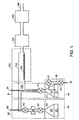
- Doses of reactants whose vapor pressures are higher than the pressure in the deposition chamber can be introduced using apparatus such as that illustrated in FIG. 1 .
- water has a vapor pressure (about 24 Torr at room temperature) that is much higher than a typical pressure in the deposition chamber (usually less than 1 Torr).
- Such a volatile precursor 20 has vapor 30 that is introduced into the heated deposition chamber 110 by the use of a pair of air-actuated diaphragm valves, 50 and 70 (Titan II model made by Parker-Hannifin, Richmond CA).
- the valves are connected by a chamber 60 having a measured volume V, and this assembly is placed inside an oven 80 held at a controlled temperature T 2 .
- the pressure of the reactant vapor 30 in the precursor reservoir 10 is equal to the equilibrium vapor pressure P eq of the solid or liquid reactant 20 at a temperature T 1 determined by the surrounding oven 40.
- the temperature T 1 is chosen to be high enough so that the precursor pressure P eq is higher than the pressure P dep in the deposition chamber.
- the temperature T 2 is chosen to be higher than T 1 so that only vapor and no condensed phase is present in the valves 50 and 70 or the chamber 60.
- this delivery method can also be used.
- the gas pressure in volume V can be set in this case by a pressure regulator (not shown) that reduces its pressure from the pressure in the vessel storing the gaseous reactant.
- Carrier gas (such as nitrogen gas) flows at a controlled rate into inlet 90 in order to speed the flow of the reactants into the deposition chamber and the purging of reaction byproducts and un-reacted reactant vapor.
- a static mixer may be placed in the tubing 100 leading into the reactor, to provide a more uniform concentration of the precursor vapor in the carrier gas as it enters the deposition chamber 110 heated by furnace 120 and containing one or more substrates 130.
- the reaction byproducts and un-reacted reactant vapors are removed by trap 140 before passing into a vacuum pump 150.
- Carrier gas exits from exhaust 160.
- valve 70 is opened so that the pressure inside chamber 60 is reduced to a value P dep close to that of the deposition chamber 110. Then valve 70 is closed and valve 50 is opened to admit precursor vapor from precursor reservoir 10 into chamber 60. Then valve 50 is closed so that the volume V of chamber 60 contains vapor of the precursor at a pressure P eq . Finally, valve 70 is opened to admit most of the precursor vapor contained in chamber 60 into the deposition chamber.
- This cycle of delivering precursor 20 is repeated if necessary until the required dose of precursor 20 has been delivered into the reaction chamber.
- the dose of precursor 20 delivered by this cycle (or several such cycles repeated to give a larger dose) is chosen to be large enough to cause the surface reactions to go to completion (also called “saturation").
- the methods described above will not deliver any precursor vapor into the deposition chamber.
- the vapor pressure can be increased by raising the temperature of the reservoir, but in some cases a higher temperature would result in thermal decomposition of the precursor.
- Metal amidinate precursors often have vapor pressures that are less than the operating pressure in the deposition chamber.
- a thermally sensitive precursor 21 with low vapor pressure its vapor 31 may be delivered using the apparatus in FIG. 1 .
- the chamber 19 is first pressurized with carrier gas delivered through tube 15 and valve 17 from a pressure controller (not shown). Valve 17 is then closed and valve 51 opened to allow the carrier gas to pressurize precursor reservoir 11 to pressure P tot .
- the mole fraction of precursor vapor in the vapor space 31 of reservoir 11 is then P eq /P tot .
- Valve 51 is closed and then valve 71 opened to deliver the dose of reactant vapor 31.
- the apparatus of FIG. 1 may include two delivery chambers that are alike, e.g., both are used to deliver samples having vapor pressures higher than or lower than the deposition pressure.
- an isothermal deposition zone 110 material is generally deposited on all surfaces exposed to the precursor vapors, including substrates and the interior chamber walls. Thus it is appropriate to report the precursor doses used in terms of moles divided by the total area of the substrates and exposed chamber walls. In some cases, deposition also occurs on part or all of the back side of the substrates, in which case that area should also be included in the to tal area.
- MgCl 2 , SrCl 2 , TiCl 3 , VCl 3 , BiCl 3 , RuCl 3 , Me 3 Al (trimethylalaminum), (CF 3 SO 3 ) 3 La (La triflate), La and Pr were used as received from Aldrich Chemical Company.
- the metal compounds produced by these procedures generally react with moisture and/of oxygen in the ambient air, and should be stored and handled under an inert, dry atmosphere such as pure nitrogen or argon gas.
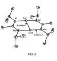
- a [Cu( i Pr-AMD)] 2 crystal was structurally characterizes by X-ray crystallography.
- [Cu( i Pr-AMD)] 2 shown in Fig. 2 , is a dimer in the solid state in which amidinate ligands badge copper metal atoms in a ⁇ , ⁇ 1 : ⁇ 1 -fashion.
- the average Cu-N distance is 1.860(1) ⁇ .
- the geometries of the five-membered rings of Cu-N-C-N-Cu are planar with centrosymmetry imposed by the crystal structure.
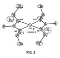
- Example 2 Synthesis of bis( N,N' -diisopropylacetamidinato)cobalt ([Co( i Pr-AMD) 2 ]). This compound was obtained in a similar manner as described for [Cu( i Pr-AMD)], but with a 1:1 mixture of ether and THF as solvent. Recrystallization in hexanes at -30 °C gave dark green crystals as product (77%). Sublimation: 40 °C at 50 mTorr (6.7 Pa). m.p.: 72 °C. Anal. Calcd for C 16 H 34 N 4 Co: C, 56.29, H, 10.04; N. 16.41. Found: C, 54.31; H, 9.69; N, 15.95.
- Co( i Pr-AMD) 2 shown in Fig. 3 , is monomeric with two amidinate ligands arranged about each cobalt atom in a distorted tetrahedral environment.
- the average Co-N distance is 2.012(8) ⁇ (0.2012(8) nm).
- the Co-N-C-N four-membered rings are planar with an imposed mirror plane.
- This compound was obtained in a manner similar to ([Co( i Pr-AMD) 2 ]) in Example 2, using 1,3-di- tert -butylcarbodiimide in place of 1,3-diisopropylcarbodiimide. Dark blue crystals (84%). Sublimation: 45 °C at 50 mtorr. (6.67 Pa) m.p.: 90 °C. Anal. Calcd for C 20 H 42 N 4 Co: C, 60.43; H, 10.65; N, 14.09. Found: C, 58.86; H, 10.33; N, 14.28.
- Example 5 Synthesis of lanthanum tris( N,N '-diisopropyl-2-tert-burylamidinate) ([La( i Pr- t BuAMD) 3 ]•1/2 C 6 H 12 ).
- Example 14 Atomic layer deposition of copper metal.
- Fig. 1 The apparatus of Fig. 1 was used to deposit copper metal. Copper(I) N,N'- diisopropylacetamidinate dimer was placed in a stainless steel container 11 with vapor volume 125 cubic centimeters and heated to 85°C, at which temperature it has a vapor pressure of about 0.15 Torr (2.00 Pa). Doses of 1.0 micromoles of the copper precursor were introduced by pressurizing the chamber to 10 Torr (1300 Pa) with nitrogen carrier gas. Hydrogen was introduced in doses of 1.4 millimole using a gas-chromatography sampling valve. The area of the substrates 130 and the heated walls of chamber 110 add up to about 10 3 square centimeters.
- a dose of copper precursor was 1 x 10 -9 moles/cm 2 and a dose of hydrogen was 1.4 x 10 -6 moles/cm 2 .
- the "exposure” is defined as the product of the partial pressure of a precursor vapor in the deposition zone and the time that this vapor is in contact with a given point on the surface of the substrate.
- the exposure of the substrate to the copper precursor was 2.3 x 10 4 Langmuirs/cycle and its exposure to hydrogen was 3.4 x 10 7 Langmuirs/cycle.
- One silicon substrate 130 was prepared by dissolving its native oxide by placing it in dilute hydrofluoric acid solution for a few seconds. Next the substrate was irradiated by ultraviolet light (e.g. UV mercury lamp) in air until the surface became hydrophilic (about two minutes). Then a substrate 130 was placed in chamber 110 and heated to a temperature of 225 °C. Another silicon substrate with narrow holes (4.5:1 ratio of length to diameter) was treated similarly and placed in chamber 110. Substrates of glassy carbon were cleaned with 10% aq. HF (5s), deionized water (30s), and isopropanol (10s) prior to drying and UV cleaning. Substrates of glass and sputtered platinum and copper on silicon were cleaned with isopropanol (10s) and dried.
- ultraviolet light e.g. UV mercury lamp
- Carrier gas flowed for 10 seconds between the alternating doses of copper precursor and hydrogen. 500 cycles were completed, and then the heater for the deposition chamber was turned off. After the substrates cooled to room temperature, they were removed from the reactor. The carbon and silicon substrates were examined by Rutherford Backscattering Spectroscopy and found to have a film of pure copper, 8 x 10 16 atoms/cm 2 thick or 1.4 x 10 -7 moles/cm 2 thick.
- the silicon wafer with the holes was cleaved and a scanning electron micrograph (SEM) was taken of a cross section of the holes.
- SEM scanning electron micrograph
- the micrograph in Fig. 4 shows that copper coats the entire inside surface of the holes with aspect ratio (defined as the ratio of length to diameter) of about 10:1; thus this process for ALD of copper demonstrates excellent step coverage.
- Example 15 Demonstration that the surface reactions are self-limited.
- Example 14 was repeated, except that the doses of both reactants were doubled.
- the film thickness and its properties were unchanged from those of Example 1. This result shows that the surface reactions are self-limiting.
- Example 16 Demonstration that the film thickness varies linearly with the number of cycles.
- Example 14 was repeated, except that 1000 cycles were used instead of 500 cycles. Twice as much material was deposited. This result shows that each self-limiting reaction reproduces the conditions needed for the other reaction to begin again, and that there are no significant delays in initiating reactions or nucleating growth on the surface of the substrate.
- Example 17 Demonstration of a range of temperatures for atomic layer deposition of copper.
- Example 14 was repeated, except that the substrate temperatures were varied within the range from 180 °C to 300 °C. Similar results were obtained, except that the thickness per cycle varied with temperature as shown in FIG. 6 . At substrate temperatures below 180 °C, no deposition of copper was observed. This observation shows that walls of a reaction chamber remain free of unwanted copper deposits if the wall temperature is kept below 180 °C and above the dew point of the precursor.
- Example 18 Atomic layer deposition of cobalt metal.
- Example 14 was repeated, except that cobalt bis( N,N' -diisopropylacetamidinate) kept at 75°C was used in place of the copper precursor and the substrate temperature was raised to 300 °C.
- a silicon substrate previously coated with silicon dioxide and then with tungsten nitride was placed in the deposition chamber, along with a fused silica capillary tube having inner diameter 20 micrometers.
- the dose of cobalt precursor was 4 x 10 -9 moles/cm 2 and the dose of hydrogen was 9 x 10 -7 moles/cm 2 .
- the exposure of the substrates to the cobalt precursor was 1 x 10 5 Langmuirs/cycle and their exposure to hydrogen was 2 x 10 7 Langmuirs/cycle.
- the substrates were examined by Rutherford Backscattering Spectroscopy and found to have a film of pure cobalt metal, 5 x 10 16 atoms/cm 2 thick or 8 x 10 -8 moles/cm 2 thick.
- the coated fused silica capillary was examined by optical microscopy, which showed that the cobalt film extended to at least 60 diameters (i.e. an aspect ratio >60) into the hole in the tubing.
- 1 points to the open end of the hole, and 2 shows how far the coating penetrated into the hole. This result demonstrates the excellent step coverage achieved by this process for ALD of cobalt.
- Example 19 Demonstration of a range of temperatures for atomic layer deposition of cobalt.
- Example 18 was repeated, except that the substrate temperature was varied between 250 and 350 °C. Similar results were obtained, except that the thickness per cycle varied with temperature as shown in FIG. 7 . At substrate temperatures below 250 °C, no deposition of cobalt was observed. This observation shows that walls of a reaction chamber remain free of unwanted cobalt deposits if the wall temperature is kept below 250 °C and above the dew point of the precursor.
- Example 20 Atomic layer deposition of an adherent copper film on a Co/WN glue layer/diffusion barrier.
- Example 14 and Example 18 were repeated one after the other on a tungsten nitride (WN) layer previously coated onto silicon dioxide, WN/SiO 2 /Si.
- WN tungsten nitride
- Adhesive tape was then applied to the surface of this multi-layer structure. No loss of adhesion was observed when the tape was pulled off.
- Example 21 Atomic layer deposition of cobalt oxide
- Example 18 was repeated, except that the hydrogen gas was replaced with water vapor. A uniform, smooth layer of cobalt oxide with composition approximately CoO was deposited.
- Example 22 Atomic layer deposition of metallic nickel.
- Example 14 was repeated, except that nickel bis( N,N' -diisopropylacetamidinate) kept at 75°C was used in place of the copper precursor and the substrate temperature was raised to 280 °C.
- the dose of nickel precursor was 4 x 10 -9 moles/cm 2 and the dose of hydrogen was 8 x 10 -7 moles/cm 2 .
- the exposure of the substrates to the nickel precursor was 3 x 10 4 Langmuirs/cycle and their exposure to hydrogen was 7 x 10 6 Langmuirs/cycle.
- the substrates were examined by Rutherford Backscattering Spectroscopy and found to have a film of pure nickel metal, 5 x 10 16 atoms/cm 2 thick or 8 x 10 -8 moles/cm 2 thick.
- Example 23 Atomic layer deposition of metallic iron.
- Example 14 was repeated, except that iron bis( N,N' -di- tert -butylacetamidinate) kept at 75°C was used in place of the copper precursor and the substrate temperature was raised to 280 °C.
- the dose of iron precursor was 4 x 10 -9 moles/cm 2 and the dose of hydrogen was 4 x 10 -6 moles/cm 2 .
- the exposure of the substrates to the iron precursor was 8 x 10 4 Langmuirs/cycle and their exposure to hydrogen was 4 x 10 7 Langmuirs/cycle.
- the substrates were examined by Rutherford Backscattering Spectroscopy and found to have a film of pure iron metal, 5 x 10 16 atoms/cm 2 thick or 8 x 10 -8 moles/cm 2 thick.
- Example 24 ALD of iron oxide.
- Example 21 was repeated, with bis( N,N' -di- tert -butylacetamidinato)iron ([Fe( t Bu-AMD) 2 ]) kept at 85°C in place of cobalt bis( N,N' -diisopropylacetamidinate).
- the dose of iron precursor was 4 x 10 -9 moles/cm 2 and the dose of water vapor was 8 x 10 -8 moles/cm 2 .
- the exposure of the substrates to the iron precursor was 8 x 10 4 Langmuirs/cycle and their exposure to water vapor was 7 x 10 5 Langmuirs/cycle.
- a uniform, smooth layer of iron oxide with composition approximately FeO was deposited on substrates heated to 250 °C.
- Example 25 ALD of Lanthanum Oxide.
- Example 21 was repeated, with tris( N,N' -diisopropylacetamidinato)lanthanum ([La( i Pr-AMD) 3 ]) kept at 120°C in place of cobalt bis( N,N' -diisopropylacetamidinate).
- the dose of lanthanum precursor was 4 x 10 -9 moles/cm 2 and the dose of water vapor was 8 x 10 -8 moles/cm 2 .
- the exposure of the substrates to the lanthanum precursor was 3 x 10 4 Langmuirs/cycle and their exposure to water vapor was 7 x 10 5 Langmuirs/cycle.
- a uniform, smooth layer of lanthanum oxide about 5 nm thick, with composition approximately La 2 O 3 was deposited on substrates heated to 300 °C.
- Example 21 When the procedure of Example 21 was repeated with more than 50 cycles, the thickness was not uniformly distributed over samples in different parts of the reaction chamber, and the thickness per cycle was larger than 0.1 nm per cycle, particularly in the region near the exhaust to the vacuum pump. It is our interpretation of this effect that water vapor was absorbed into the bulk of the thicker lanthanum oxide layer during the water dose. During the few seconds of purge time following the water pulse some, but not all, of the adsorbed water was released back into the nitrogen gas and carried out of the chamber. However, further release of water vapor continued during the next dose of lanthanum precursor.
- Example 26 ALD of Lanthanum Oxide/ Aluminum Oxide nanolaminate.
- Example 25 was repeated to deposit 16 cycles of lanthanum oxide. Then 6 cycles of aluminum oxide were deposited by ALD using alternating doses of trimethylaluminum vapor and water vapor, according to a process well-known in the art. This pattern of (16 La 2 O 3 + 6 Al 2 O 3 ) cycles was repeated 5 times. A uniform, smooth layer about 10 nm thick was deposited on substrates heated to 300 °C. The layers had average composition approximately LaAlO 3 . Capacitors made of this material had a dielectric constant about 18 and very low leakage current of about 5 x 10 -8 amperes per square centimeter at an applied potential of 1 volt.
- Example 26 Our interpretation of the thickness uniformity achieved in Example 26 is that the aluminum oxide layers act as a barrier to diffusion of water into the lower layers of lanthanum oxide. Thus the thickness uniformity expected of an ALD process is achieved for the La 2 O 3 /Al 2 O 3 nanolaminate for any desired thickness.
- Example 27 ALD of Manganese Oxide.
- Example 21 was repeated, with bis( N,N' - tert -butylacetamidinato)manganese ([Mn( t Bu-AMD) 2 ]) kept at 75°C in place of cobalt bis( N,N' -diisopropylacetamidinate).
- the dose of manganese precursor was 4 x 10 -9 moles/cm 2 and the dose of water vapor was 8 x 10 -8 moles/cm 2 .
- the exposure of the substrates to the manganese precursor was 3 x 10 4 Langmuirs/cycle and their exposure to water vapor was 6 x 10 5 Langmuirs/cycle.
- a uniform, smooth layer of manganese(II) oxide with composition approximately MnO was deposited on substrates heated to 250 °C at a deposition rate of about 0.1 nanometer per cycle.
- Example 28 ALD of Magnesium Oxide.
- Example 21 was repeated, with bis( N,N' - tert -butylacetamidinato)magnesium ([Mg( t Bu-AMD) 2 ]), prepared by a procedure similar to that described in Example 3, kept at 80°C in place of the cobalt bis( N,N' -diisopropylacetamidinate) used in Example 21.
- the dose of magnesium precursor was 3 x 10 -9 moles/cm 2 and the dose of water vapor was 6 x 10 -8 moles/cm 2 .
- the exposure of the substrates to the magnesium precursor was 3 x 10 4 Langmuirs/cycle and their exposure to water vapor was 5 x 10 5 Langmuirs/cycle.
- a uniform, smooth layer of magnesium oxide with composition approximately MgO was deposited on substrates heated to 250 °C at a deposition rate of 0.08 nanometer per cycle.
- Example 29 Synthesis of lithium N,N' -di- sec -butylacetamidinate.
- Example 30 Synthesis of cobalt bis( N,N' -di- sec -butylacetamidinate) ([Co( sec -Bu-AMD) 2 ]).
- Example 31 Synthesis of copper(I) N,N' -di- sec -butylacetamidinate dimer ([Cu( sec -Bu-AMD)] 2 ).
- Example 30 The procedure of Example 30 was used with one equivalent of copper (I) chloride, CuCl, in place of the cobalt chloride and one equivalent of the lithium N,N' -di- sec- butylacetamidinate prepared in Example 29.
- [Cu( sec -Bu-AMD)] 2 was isolated by the procedure of Example 30. Sublimation: 55 °C at 50 mtorr. (6.67 Pa) mp. 77 °C.
- [Cu( sec -Bu-AMD)] 2 has an advantage as a precursor for ALD of copper in that it is a liquid at the temperature used for vaporization (about 100 °C), resulting in more reproducible delivery of vapor than was obtained by sublimation of solid precursors.
- Example 32 Synthesis of bismuth tris( N,N' -di- tert -butylacetamidinate) dimer ([Bi( t Bu-AMD) 3 ] 2 ).
- Example 33 Synthesis of strontium bis( N,N' -di- tert -butylacetamidinate) ([Sr( t Bu-AMD) 2 ] n ).
- Example 34 ALD of Bismuth Oxide, Bi 2 O 3 .
- films of bismuth oxide, Bi 2 O 3 were deposited on substrates at a temperature of 200 °C from a vapor source containing bismuth tris( N,N' -di- tert -butylacetamidinate) at 85 °C.
- the thickness of the films was about 0.03 nanometers per cycle.
- Example 35 Synthesis of tris( N,N' -diisopropylacetamidinato)ruthenium ([Ru( i Pr-AMD) 3 ]).
- Example 14 was repeated using only the copper precursor, and no hydrogen gas. No film was observed to have been deposited on the substrate surface.
- Example 18 was repeated using only the cobalt precursor, and no hydrogen. No film was observed to have been deposited on the substrate surface.
Landscapes
- Chemical & Material Sciences (AREA)
- Organic Chemistry (AREA)
- Metallurgy (AREA)
- Engineering & Computer Science (AREA)
- Materials Engineering (AREA)
- Mechanical Engineering (AREA)
- Chemical Kinetics & Catalysis (AREA)
- General Chemical & Material Sciences (AREA)
- Inorganic Chemistry (AREA)
- Chemical Vapour Deposition (AREA)
- Electrodes Of Semiconductors (AREA)
- Formation Of Insulating Films (AREA)
- Organic Low-Molecular-Weight Compounds And Preparation Thereof (AREA)
- Physical Vapour Deposition (AREA)
- Internal Circuitry In Semiconductor Integrated Circuit Devices (AREA)
Priority Applications (1)
| Application Number | Priority Date | Filing Date | Title |
|---|---|---|---|
| EP10150011.4A EP2182088B1 (en) | 2002-11-15 | 2003-11-14 | Atomic layer deposition using metal amidinates |
Applications Claiming Priority (5)
| Application Number | Priority Date | Filing Date | Title |
|---|---|---|---|
| US42697502P | 2002-11-15 | 2002-11-15 | |
| US426975P | 2002-11-15 | ||
| US46336503P | 2003-04-16 | 2003-04-16 | |
| US463365P | 2003-04-16 | ||
| PCT/US2003/036568 WO2004046417A2 (en) | 2002-11-15 | 2003-11-14 | Atomic layer deposition using metal amidinates |
Publications (2)
| Publication Number | Publication Date |
|---|---|
| EP1563117A2 EP1563117A2 (en) | 2005-08-17 |
| EP1563117B1 true EP1563117B1 (en) | 2010-01-06 |
Family
ID=32329139
Family Applications (2)
| Application Number | Title | Priority Date | Filing Date |
|---|---|---|---|
| EP03783541A Expired - Lifetime EP1563117B1 (en) | 2002-11-15 | 2003-11-14 | Atomic layer deposition using metal amidinates |
| EP10150011.4A Expired - Lifetime EP2182088B1 (en) | 2002-11-15 | 2003-11-14 | Atomic layer deposition using metal amidinates |
Family Applications After (1)
| Application Number | Title | Priority Date | Filing Date |
|---|---|---|---|
| EP10150011.4A Expired - Lifetime EP2182088B1 (en) | 2002-11-15 | 2003-11-14 | Atomic layer deposition using metal amidinates |
Country Status (9)
| Country | Link |
|---|---|
| US (3) | US7557229B2 (enExample) |
| EP (2) | EP1563117B1 (enExample) |
| JP (6) | JP4988159B2 (enExample) |
| KR (8) | KR101266442B1 (enExample) |
| CN (3) | CN102344460B (enExample) |
| AT (1) | ATE454483T1 (enExample) |
| AU (1) | AU2003290956A1 (enExample) |
| DE (1) | DE60330896D1 (enExample) |
| WO (1) | WO2004046417A2 (enExample) |
Cited By (3)
| Publication number | Priority date | Publication date | Assignee | Title |
|---|---|---|---|---|
| EP2182088A1 (en) * | 2002-11-15 | 2010-05-05 | President and Fellows of Harvard College | Atomic layer deposition using metal amidinates |
| US20150004317A1 (en) * | 2012-07-20 | 2015-01-01 | American Air Liquide, Inc. | Organosilane precursors for ald/cvd silicon-containing film applications |
| US10259836B2 (en) * | 2015-11-30 | 2019-04-16 | Samsung Electronics Co., Ltd. | Methods of forming thin film and fabricating integrated circuit device using niobium compound |
Families Citing this family (542)
| Publication number | Priority date | Publication date | Assignee | Title |
|---|---|---|---|---|
| ATE305784T1 (de) | 1997-02-15 | 2005-10-15 | Edelstam Inc | Medikament gegen dysmenorrhoe und premenstruelles syndrom enthaltend lidocain |
| WO2004083479A2 (en) * | 2003-03-17 | 2004-09-30 | Epichem Limited | Alcoholates of rare earth mtals a precursors for metaloxide layers or films |
| US20050227007A1 (en) | 2004-04-08 | 2005-10-13 | Bradley Alexander Z | Volatile copper(I) complexes for deposition of copper films by atomic layer deposition |
| WO2009105668A1 (en) | 2008-02-20 | 2009-08-27 | President And Fellows Of Harvard College | Bicyclic guanidines, metal complexes thereof and their use in vapor deposition |
| KR100519800B1 (ko) * | 2004-01-13 | 2005-10-10 | 삼성전자주식회사 | 란타늄 산화막의 제조방법 및 이를 이용한 모스 전계효과트랜지스터 및 캐패시터의 제조방법 |
| US7166732B2 (en) | 2004-06-16 | 2007-01-23 | Advanced Technology Materials, Inc. | Copper (I) compounds useful as deposition precursors of copper thin films |
| JP4639686B2 (ja) * | 2004-07-27 | 2011-02-23 | Jsr株式会社 | 化学気相成長材料及び化学気相成長方法 |
| EP1771594A1 (en) * | 2004-07-30 | 2007-04-11 | E.I.Du pont de nemours and company | Copper (i) complexes for deposition of copper films by atomic layer deposition |
| KR100589040B1 (ko) | 2004-08-05 | 2006-06-14 | 삼성전자주식회사 | 막 형성방법 및 이를 이용한 반도체 장치의 커패시터제조방법 |
| KR100643637B1 (ko) * | 2005-01-25 | 2006-11-10 | 한국화학연구원 | 니켈 아미노알콕사이드 선구 물질을 사용하는 원자층침착법으로 니켈 산화물 박막을 제조하는 방법 |
| US7064224B1 (en) | 2005-02-04 | 2006-06-20 | Air Products And Chemicals, Inc. | Organometallic complexes and their use as precursors to deposit metal films |
| US7816550B2 (en) * | 2005-02-10 | 2010-10-19 | Praxair Technology, Inc. | Processes for the production of organometallic compounds |
| JP2006328034A (ja) * | 2005-05-30 | 2006-12-07 | Nippon Zeon Co Ltd | 遷移金属錯体、環状オレフィン重合用触媒、および環状オレフィン重合体の製造方法 |
| WO2007015436A1 (ja) * | 2005-08-04 | 2007-02-08 | Tosoh Corporation | 金属含有化合物、その製造方法、金属含有薄膜及びその形成方法 |
| US7776394B2 (en) | 2005-08-08 | 2010-08-17 | E.I. Du Pont De Nemours And Company | Atomic layer deposition of metal-containing films using surface-activating agents |
| KR100704914B1 (ko) * | 2005-08-24 | 2007-04-06 | 한국화학연구원 | 니켈 아미노알콕사이드 선구 물질을 사용하여 금속 유기물화학 증착법으로 니켈 산화물 박막을 제조하는 방법 |
| US7767114B2 (en) | 2006-02-07 | 2010-08-03 | President And Fellows Of Harvard College | Gas-phase functionalization of carbon nanotubes |
| KR20140139636A (ko) | 2006-03-10 | 2014-12-05 | 어드밴스드 테크놀러지 머티리얼즈, 인코포레이티드 | 티타네이트, 란타네이트 및 탄탈레이트 유전막의 원자층 증착 및 화학 증기 증착용 전구체 조성물 |
| US8288198B2 (en) * | 2006-05-12 | 2012-10-16 | Advanced Technology Materials, Inc. | Low temperature deposition of phase change memory materials |
| WO2007142700A1 (en) * | 2006-06-02 | 2007-12-13 | Advanced Technology Materials, Inc. | Copper (i) amidinates and guanidinates for forming copper thin films |
| JP2008013533A (ja) * | 2006-06-07 | 2008-01-24 | Toyota Motor Corp | アミジン−カルボン酸錯体及び複数錯体含有化合物 |
| US20090208637A1 (en) * | 2006-06-15 | 2009-08-20 | Advanced Technology Materials, Inc. | Cobalt precursors useful for forming cobalt-containing films on substrates |
| US7638645B2 (en) | 2006-06-28 | 2009-12-29 | President And Fellows Of Harvard University | Metal (IV) tetra-amidinate compounds and their use in vapor deposition |
| WO2008002546A1 (en) | 2006-06-28 | 2008-01-03 | President And Fellows Of Harvard College | Metal(iv) tetra-amidinate compounds and their use in vapor deposition |
| US7547631B2 (en) * | 2006-07-31 | 2009-06-16 | Rohm And Haas Electronic Materials Llc | Organometallic compounds |
| US7781016B2 (en) * | 2006-08-23 | 2010-08-24 | Applied Materials, Inc. | Method for measuring precursor amounts in bubbler sources |
| WO2008034468A1 (en) | 2006-09-22 | 2008-03-27 | L'air Liquide Societe Anonyme Pour L'etude Et L'exploitation Des Procedes Georges Claude | Method for the deposition of a ruthenium containing film |
| KR101279925B1 (ko) | 2006-11-02 | 2013-07-08 | 어드밴스드 테크놀러지 머티리얼즈, 인코포레이티드 | 금속 박막의 cvd/ald용으로 유용한 안티몬 및 게르마늄 착체 |
| US7776395B2 (en) * | 2006-11-14 | 2010-08-17 | Applied Materials, Inc. | Method of depositing catalyst assisted silicates of high-k materials |
| US7749574B2 (en) * | 2006-11-14 | 2010-07-06 | Applied Materials, Inc. | Low temperature ALD SiO2 |
| JP2008182183A (ja) * | 2006-12-26 | 2008-08-07 | Doshisha | 原子層成長法を用いた成膜方法及びその成膜装置 |
| WO2008088563A2 (en) * | 2007-01-17 | 2008-07-24 | Advanced Technology Materials, Inc. | Precursor compositions for ald/cvd of group ii ruthenate thin films |
| US7750173B2 (en) | 2007-01-18 | 2010-07-06 | Advanced Technology Materials, Inc. | Tantalum amido-complexes with chelate ligands useful for CVD and ALD of TaN and Ta205 thin films |
| US7851360B2 (en) * | 2007-02-14 | 2010-12-14 | Intel Corporation | Organometallic precursors for seed/barrier processes and methods thereof |
| CN101617065B (zh) | 2007-02-21 | 2011-11-23 | 乔治洛德方法研究和开发液化空气有限公司 | 在基底上形成钌基薄膜的方法 |
| US7964746B2 (en) * | 2007-03-30 | 2011-06-21 | Advanced Technology Materials, Inc. | Copper precursors for CVD/ALD/digital CVD of copper metal films |
| US7858525B2 (en) * | 2007-03-30 | 2010-12-28 | Intel Corporation | Fluorine-free precursors and methods for the deposition of conformal conductive films for nanointerconnect seed and fill |
| EP2857549A3 (en) * | 2007-04-09 | 2015-07-15 | President and Fellows of Harvard College | Chemical vapour deposition of thin films using metal amidinate precursors |
| KR20100016477A (ko) * | 2007-04-12 | 2010-02-12 | 어드밴스드 테크놀러지 머티리얼즈, 인코포레이티드 | Ald/cvd용의 지르코늄, 하프늄, 티타늄 및 규소 전구체 |
| JP2009016782A (ja) * | 2007-06-04 | 2009-01-22 | Tokyo Electron Ltd | 成膜方法及び成膜装置 |
| JP5437594B2 (ja) * | 2007-06-05 | 2014-03-12 | ローム・アンド・ハース・エレクトロニック・マテリアルズ,エル.エル.シー. | 有機金属化合物 |
| KR101593352B1 (ko) | 2007-06-28 | 2016-02-15 | 인티그리스, 인코포레이티드 | 이산화규소 간극 충전용 전구체 |
| US8142847B2 (en) | 2007-07-13 | 2012-03-27 | Rohm And Haas Electronic Materials Llc | Precursor compositions and methods |
| WO2009012341A2 (en) * | 2007-07-16 | 2009-01-22 | Advancaed Technology Materials, Inc. | Group iv complexes as cvd and ald precursors for forming metal-containing thin films |
| US7659414B2 (en) * | 2007-07-20 | 2010-02-09 | Rohm And Haas Company | Method of preparing organometallic compounds |
| WO2009013721A1 (en) * | 2007-07-24 | 2009-01-29 | L'air Liquide-Societe Anonyme Pour L'etude Et L'exploitation Des Procedes Georges Claude | Ruthenium precursor with two differing ligands for use in semiconductor applications |
| US8455049B2 (en) | 2007-08-08 | 2013-06-04 | Advanced Technology Materials, Inc. | Strontium precursor for use in chemical vapor deposition, atomic layer deposition and rapid vapor deposition |
| US20090087561A1 (en) * | 2007-09-28 | 2009-04-02 | Advanced Technology Materials, Inc. | Metal and metalloid silylamides, ketimates, tetraalkylguanidinates and dianionic guanidinates useful for cvd/ald of thin films |
| US8834968B2 (en) | 2007-10-11 | 2014-09-16 | Samsung Electronics Co., Ltd. | Method of forming phase change material layer using Ge(II) source, and method of fabricating phase change memory device |
| KR101458953B1 (ko) | 2007-10-11 | 2014-11-07 | 삼성전자주식회사 | Ge(Ⅱ)소오스를 사용한 상변화 물질막 형성 방법 및상변화 메모리 소자 제조 방법 |
| US20100279011A1 (en) * | 2007-10-31 | 2010-11-04 | Advanced Technology Materials, Inc. | Novel bismuth precursors for cvd/ald of thin films |
| SG178736A1 (en) | 2007-10-31 | 2012-03-29 | Advanced Tech Materials | Amorphous ge/te deposition process |
| US8894723B2 (en) * | 2007-12-28 | 2014-11-25 | Universitetet I Oslo | Formation of a lithium comprising structure on a substrate by ALD |
| US20090199739A1 (en) * | 2008-01-24 | 2009-08-13 | Thompson David M | Organometallic compounds, processes for the preparation thereof and methods of use thereof |
| US20090215225A1 (en) | 2008-02-24 | 2009-08-27 | Advanced Technology Materials, Inc. | Tellurium compounds useful for deposition of tellurium containing materials |
| US8852460B2 (en) | 2008-03-19 | 2014-10-07 | Air Liquide Electronics U.S. Lp | Alkali earth metal precursors for depositing calcium and strontium containing films |
| US7932176B2 (en) | 2008-03-21 | 2011-04-26 | President And Fellows Of Harvard College | Self-aligned barrier layers for interconnects |
| CN101981226B (zh) | 2008-03-26 | 2012-09-26 | 乔治洛德方法研究和开发液化空气有限公司 | 含有钌和碱土金属的三元氧化物膜的沉积 |
| FR2929449A1 (fr) * | 2008-03-28 | 2009-10-02 | Stmicroelectronics Tours Sas S | Procede de formation d'une couche d'amorcage de depot d'un metal sur un substrat |
| US8674127B2 (en) | 2008-05-02 | 2014-03-18 | Advanced Technology Materials, Inc. | Antimony compounds useful for deposition of antimony-containing materials |
| TWI467045B (zh) * | 2008-05-23 | 2015-01-01 | Sigma Aldrich Co | 高介電常數電介質薄膜與使用鈰基前驅物製造高介電常數電介質薄膜之方法 |
| TW200949939A (en) * | 2008-05-23 | 2009-12-01 | Sigma Aldrich Co | High-k dielectric films and methods of producing using titanium-based β -diketonate precursors |
| US20120156373A1 (en) | 2008-06-05 | 2012-06-21 | American Air Liquide, Inc. | Preparation of cerium-containing precursors and deposition of cerium-containing films |
| TWI565827B (zh) * | 2008-06-05 | 2017-01-11 | 液態空氣喬治斯克勞帝方法研究開發股份有限公司 | 含鑭系元素前驅物的製備和含鑭系元素薄膜的沈積 |
| CN102057077B (zh) * | 2008-06-05 | 2013-11-13 | 乔治洛德方法研究和开发液化空气有限公司 | 含镧系元素的前体的制备和含镧系元素的薄膜的沉积 |
| US20110180905A1 (en) * | 2008-06-10 | 2011-07-28 | Advanced Technology Materials, Inc. | GeSbTe MATERIAL INCLUDING SUPERFLOW LAYER(S), AND USE OF Ge TO PREVENT INTERACTION OF Te FROM SbXTeY AND GeXTeY RESULTING IN HIGH Te CONTENT AND FILM CRYSTALLINITY |
| US8168811B2 (en) | 2008-07-22 | 2012-05-01 | Advanced Technology Materials, Inc. | Precursors for CVD/ALD of metal-containing films |
| US8105937B2 (en) * | 2008-08-13 | 2012-01-31 | International Business Machines Corporation | Conformal adhesion promoter liner for metal interconnects |
| WO2010065874A2 (en) | 2008-12-05 | 2010-06-10 | Atmi | High concentration nitrogen-containing germanium telluride based memory devices and processes of making |
| US7927942B2 (en) | 2008-12-19 | 2011-04-19 | Asm International N.V. | Selective silicide process |
| US9379011B2 (en) | 2008-12-19 | 2016-06-28 | Asm International N.V. | Methods for depositing nickel films and for making nickel silicide and nickel germanide |
| CN102326213A (zh) * | 2009-02-18 | 2012-01-18 | 东洋纺织株式会社 | 金属薄膜制造方法以及金属薄膜 |
| JP2010209425A (ja) * | 2009-03-11 | 2010-09-24 | Tokyo Electron Ltd | Cu膜の成膜方法および記憶媒体 |
| US9394608B2 (en) | 2009-04-06 | 2016-07-19 | Asm America, Inc. | Semiconductor processing reactor and components thereof |
| JP5530118B2 (ja) * | 2009-04-08 | 2014-06-25 | 東京エレクトロン株式会社 | 酸化マンガン膜の形成方法、半導体装置の製造方法および半導体装置 |
| KR101329449B1 (ko) | 2009-05-22 | 2013-11-14 | 어드밴스드 테크놀러지 머티리얼즈, 인코포레이티드 | 저온 gst 방법 |
| US8410468B2 (en) * | 2009-07-02 | 2013-04-02 | Advanced Technology Materials, Inc. | Hollow GST structure with dielectric fill |
| EP2451989A2 (en) | 2009-07-10 | 2012-05-16 | L'Air Liquide Société Anonyme pour l'Etude et l'Exploitation des Procédés Georges Claude | Bis-ketoiminate copper precursors for deposition of copper-containing films |
| SG178267A1 (en) * | 2009-08-07 | 2012-03-29 | Sigma Aldrich Co Llc | High molecular weight alkyl-allyl cobalttricarbonyl complexes and use thereof for preparing dielectric thin films |
| US8802201B2 (en) | 2009-08-14 | 2014-08-12 | Asm America, Inc. | Systems and methods for thin-film deposition of metal oxides using excited nitrogen-oxygen species |
| WO2011027835A1 (ja) * | 2009-09-02 | 2011-03-10 | 株式会社アルバック | Co膜の形成方法 |
| KR20120046786A (ko) | 2009-09-02 | 2012-05-10 | 가부시키가이샤 알박 | Co 막의 형성 방법 및 Cu 배선막의 형성 방법 |
| EP2339048B1 (en) | 2009-09-14 | 2016-12-07 | Rohm and Haas Electronic Materials, L.L.C. | Method for depositing organometallic compounds |
| JP2011066060A (ja) * | 2009-09-15 | 2011-03-31 | Tokyo Electron Ltd | 金属シリサイド膜の形成方法 |
| JP5225957B2 (ja) * | 2009-09-17 | 2013-07-03 | 東京エレクトロン株式会社 | 成膜方法および記憶媒体 |
| KR20120062915A (ko) * | 2009-09-29 | 2012-06-14 | 도쿄엘렉트론가부시키가이샤 | 니켈막의 성막 방법 |
| CN102859662B (zh) | 2009-10-23 | 2015-11-25 | 哈佛大学校长及研究员协会 | 用于互连的自对准阻挡层和封盖层 |
| US20110124182A1 (en) * | 2009-11-20 | 2011-05-26 | Advanced Techology Materials, Inc. | System for the delivery of germanium-based precursor |
| WO2011106072A2 (en) | 2010-02-23 | 2011-09-01 | L'air Liquide Societe Anonyme Pour L'etude Et L'exploitation Des Procedes Georges Claude | Use of ruthenium tetroxide as a precursor and reactant for thin film depositions |
| KR101706809B1 (ko) | 2010-03-26 | 2017-02-15 | 엔테그리스, 아이엔씨. | 게르마늄 안티몬 텔루라이드 물질 및 이를 포함하는 장치 |
| US8796483B2 (en) | 2010-04-01 | 2014-08-05 | President And Fellows Of Harvard College | Cyclic metal amides and vapor deposition using them |
| US8357614B2 (en) | 2010-04-19 | 2013-01-22 | L'air Liquide Societe Anonyme Pour L'etude Et L'exploitation Des Procedes Georges Claude | Ruthenium-containing precursors for CVD and ALD |
| US9190609B2 (en) | 2010-05-21 | 2015-11-17 | Entegris, Inc. | Germanium antimony telluride materials and devices incorporating same |
| TWI529808B (zh) | 2010-06-10 | 2016-04-11 | Asm國際股份有限公司 | 使膜選擇性沈積於基板上的方法 |
| EP2636674B1 (en) * | 2010-11-02 | 2016-04-06 | Ube Industries, Ltd. | (amide amino alkane) metal compound and method of producing metal-containing thin film using said metal compound |
| TWI481615B (zh) | 2011-03-11 | 2015-04-21 | Applied Materials Inc | 用於錳的原子層沉積之前驅物及方法 |
| US8871617B2 (en) * | 2011-04-22 | 2014-10-28 | Asm Ip Holding B.V. | Deposition and reduction of mixed metal oxide thin films |
| KR20140049988A (ko) | 2011-05-13 | 2014-04-28 | 그린센터 캐나다 | 11 족 단일-금속 전구체 화합물 및 금속 증착에서의 이의 용도 |
| US9312155B2 (en) | 2011-06-06 | 2016-04-12 | Asm Japan K.K. | High-throughput semiconductor-processing apparatus equipped with multiple dual-chamber modules |
| JP6108704B2 (ja) | 2011-07-13 | 2017-04-05 | ダウ グローバル テクノロジーズ エルエルシー | 有機金属化合物精製 |
| US10854498B2 (en) | 2011-07-15 | 2020-12-01 | Asm Ip Holding B.V. | Wafer-supporting device and method for producing same |
| US20130023129A1 (en) | 2011-07-20 | 2013-01-24 | Asm America, Inc. | Pressure transmitter for a semiconductor processing environment |
| US8525232B2 (en) | 2011-08-10 | 2013-09-03 | International Business Machines Corporation | Semiconductor structure having a wetting layer |
| EP2559682B1 (en) | 2011-08-15 | 2016-08-03 | Rohm and Haas Electronic Materials LLC | Organometallic compound preparation |
| EP2559681B1 (en) | 2011-08-15 | 2016-06-22 | Dow Global Technologies LLC | Organometallic compound preparation |
| JP5661006B2 (ja) * | 2011-09-02 | 2015-01-28 | 東京エレクトロン株式会社 | ニッケル膜の成膜方法 |
| KR101629869B1 (ko) | 2011-09-16 | 2016-06-13 | 엠파이어 테크놀로지 디벨롭먼트 엘엘씨 | 그래핀 결함의 변경 |
| KR101405256B1 (ko) * | 2011-09-16 | 2014-06-10 | 엠파이어 테크놀로지 디벨롭먼트 엘엘씨 | 그래핀 결함 변경 |
| WO2013043501A1 (en) * | 2011-09-23 | 2013-03-28 | Applied Materials, Inc. | Metal-aluminum alloy films from metal amidinate precursors and aluminum precursors |
| CN103874781B (zh) * | 2011-10-07 | 2016-02-10 | 气相成长株式会社 | 钴基膜形成方法 |
| US9017481B1 (en) | 2011-10-28 | 2015-04-28 | Asm America, Inc. | Process feed management for semiconductor substrate processing |
| JP5806912B2 (ja) * | 2011-11-08 | 2015-11-10 | 株式会社アルバック | 液体原料の気化方法 |
| JP5795520B2 (ja) * | 2011-11-14 | 2015-10-14 | 大陽日酸株式会社 | 金属薄膜材料および金属薄膜の成膜方法 |
| JP2013104100A (ja) * | 2011-11-14 | 2013-05-30 | Taiyo Nippon Sanso Corp | 金属薄膜の成膜方法および金属薄膜成膜用原料 |
| US9112003B2 (en) | 2011-12-09 | 2015-08-18 | Asm International N.V. | Selective formation of metallic films on metallic surfaces |
| US20130168614A1 (en) * | 2011-12-29 | 2013-07-04 | L'Air Liquide Société Anonyme pour ''Etude et l'Exploitation des Procédés Georges Claude | Nickel allyl amidinate precursors for deposition of nickel-containing films |
| JP5843318B2 (ja) * | 2012-02-14 | 2016-01-13 | 株式会社Adeka | Ald法用窒化アルミニウム系薄膜形成用原料及び該薄膜の製造方法 |
| JP5919882B2 (ja) * | 2012-02-27 | 2016-05-18 | 宇部興産株式会社 | コバルト化合物の混合物、及び当該コバルト化合物の混合物を用いたコバルト含有薄膜の製造方法 |
| JP5842687B2 (ja) * | 2012-03-15 | 2016-01-13 | 宇部興産株式会社 | コバルト膜形成用原料及び当該原料を用いたコバルト含有薄膜の製造方法 |
| KR102117124B1 (ko) | 2012-04-30 | 2020-05-29 | 엔테그리스, 아이엔씨. | 유전체 물질로 중심-충전된 상 변화 합금을 포함하는 상 변화 메모리 구조체 |
| US9443736B2 (en) | 2012-05-25 | 2016-09-13 | Entegris, Inc. | Silylene compositions and methods of use thereof |
| US8692010B1 (en) | 2012-07-13 | 2014-04-08 | American Air Liquide, Inc. | Synthesis method for copper compounds |
| US8859045B2 (en) | 2012-07-23 | 2014-10-14 | Applied Materials, Inc. | Method for producing nickel-containing films |
| US9194040B2 (en) | 2012-07-25 | 2015-11-24 | Applied Materials, Inc. | Methods for producing nickel-containing films |
| JP5917351B2 (ja) * | 2012-09-20 | 2016-05-11 | 東京エレクトロン株式会社 | 金属膜の成膜方法 |
| JP2014062312A (ja) * | 2012-09-24 | 2014-04-10 | Tokyo Electron Ltd | マンガンシリケート膜の形成方法、処理システム、半導体デバイスの製造方法および半導体デバイス |
| JP6008682B2 (ja) * | 2012-10-05 | 2016-10-19 | 大陽日酸株式会社 | 気相成長装置用配管のクリーニング方法 |
| US10714315B2 (en) | 2012-10-12 | 2020-07-14 | Asm Ip Holdings B.V. | Semiconductor reaction chamber showerhead |
| JP2014084506A (ja) * | 2012-10-24 | 2014-05-12 | Hitachi Kokusai Electric Inc | 基板処理方法、基板処理装置およびプログラム |
| US9640757B2 (en) | 2012-10-30 | 2017-05-02 | Entegris, Inc. | Double self-aligned phase change memory device structure |
| US20160376700A1 (en) | 2013-02-01 | 2016-12-29 | Asm Ip Holding B.V. | System for treatment of deposition reactor |
| US11326255B2 (en) | 2013-02-07 | 2022-05-10 | Uchicago Argonne, Llc | ALD reactor for coating porous substrates |
| WO2014124056A1 (en) | 2013-02-08 | 2014-08-14 | Advanced Technology Materials, Inc. | Ald processes for low leakage current and low equivalent oxide thickness bitao films |
| US9005704B2 (en) * | 2013-03-06 | 2015-04-14 | Applied Materials, Inc. | Methods for depositing films comprising cobalt and cobalt nitrides |
| JP2014236192A (ja) * | 2013-06-05 | 2014-12-15 | 東京エレクトロン株式会社 | 酸化マンガン膜の形成方法 |
| WO2014197801A1 (en) * | 2013-06-06 | 2014-12-11 | President And Fellows Of Harvard College | Vapor source using solutions of precursors in tertiary amines |
| TW201509799A (zh) | 2013-07-19 | 2015-03-16 | Air Liquide | 用於ald/cvd含矽薄膜應用之六配位含矽前驅物 |
| US9994954B2 (en) | 2013-07-26 | 2018-06-12 | Versum Materials Us, Llc | Volatile dihydropyrazinly and dihydropyrazine metal complexes |
| US9343315B2 (en) | 2013-11-27 | 2016-05-17 | Taiwan Semiconductor Manufacturing Co., Ltd. | Method for fabricating semiconductor structure, and solid precursor delivery system |
| US9099301B1 (en) * | 2013-12-18 | 2015-08-04 | L'Air Liquide, Société Anonyme pour l'Etude et l'Exploitation des Procédés Georges Claude | Preparation of lanthanum-containing precursors and deposition of lanthanum-containing films |
| TWI739285B (zh) | 2014-02-04 | 2021-09-11 | 荷蘭商Asm Ip控股公司 | 金屬、金屬氧化物與介電質的選擇性沉積 |
| KR102198856B1 (ko) | 2014-02-10 | 2021-01-05 | 삼성전자 주식회사 | 니켈 함유막을 포함하는 반도체 소자의 제조 방법 |
| US10683571B2 (en) | 2014-02-25 | 2020-06-16 | Asm Ip Holding B.V. | Gas supply manifold and method of supplying gases to chamber using same |
| US10167557B2 (en) | 2014-03-18 | 2019-01-01 | Asm Ip Holding B.V. | Gas distribution system, reactor including the system, and methods of using the same |
| US11015245B2 (en) | 2014-03-19 | 2021-05-25 | Asm Ip Holding B.V. | Gas-phase reactor and system having exhaust plenum and components thereof |
| KR102168174B1 (ko) | 2014-03-19 | 2020-10-20 | 삼성전자주식회사 | 니켈 화합물 및 이를 이용한 박막 형성 방법 |
| US10047435B2 (en) | 2014-04-16 | 2018-08-14 | Asm Ip Holding B.V. | Dual selective deposition |
| KR102193623B1 (ko) | 2014-06-05 | 2020-12-21 | 삼성전자주식회사 | 커패시터 및 그 제조 방법 |
| US9382618B2 (en) | 2014-07-18 | 2016-07-05 | UChicago Argnonne, LLC | Oxygen-free atomic layer deposition of indium sulfide |
| US10858737B2 (en) | 2014-07-28 | 2020-12-08 | Asm Ip Holding B.V. | Showerhead assembly and components thereof |
| JP6734841B2 (ja) * | 2014-08-04 | 2020-08-05 | ビーエーエスエフ ソシエタス・ヨーロピアBasf Se | 無機薄膜の生成方法 |
| US9890456B2 (en) | 2014-08-21 | 2018-02-13 | Asm Ip Holding B.V. | Method and system for in situ formation of gas-phase compounds |
| US10941490B2 (en) | 2014-10-07 | 2021-03-09 | Asm Ip Holding B.V. | Multiple temperature range susceptor, assembly, reactor and system including the susceptor, and methods of using the same |
| US9657845B2 (en) | 2014-10-07 | 2017-05-23 | Asm Ip Holding B.V. | Variable conductance gas distribution apparatus and method |
| US10570513B2 (en) | 2014-12-13 | 2020-02-25 | American Air Liquide, Inc. | Organosilane precursors for ALD/CVD silicon-containing film applications and methods of using the same |
| KR102185458B1 (ko) | 2015-02-03 | 2020-12-03 | 에이에스엠 아이피 홀딩 비.브이. | 선택적 퇴적 |
| US9490145B2 (en) | 2015-02-23 | 2016-11-08 | Asm Ip Holding B.V. | Removal of surface passivation |
| US10276355B2 (en) | 2015-03-12 | 2019-04-30 | Asm Ip Holding B.V. | Multi-zone reactor, system including the reactor, and method of using the same |
| WO2016204772A1 (en) | 2015-06-18 | 2016-12-22 | Intel Corporation | Inherently selective precursors for deposition of second or third row transition metal thin films |
| US10458018B2 (en) | 2015-06-26 | 2019-10-29 | Asm Ip Holding B.V. | Structures including metal carbide material, devices including the structures, and methods of forming same |
| US10913754B2 (en) | 2015-07-07 | 2021-02-09 | Samsung Electronics Co., Ltd. | Lanthanum compound and methods of forming thin film and integrated circuit device using the lanthanum compound |
| US10600673B2 (en) | 2015-07-07 | 2020-03-24 | Asm Ip Holding B.V. | Magnetic susceptor to baseplate seal |
| KR102551351B1 (ko) * | 2018-03-16 | 2023-07-04 | 삼성전자 주식회사 | 란타넘 화합물과 이를 이용한 박박 형성 방법 및 집적회로 소자의 제조 방법 |
| KR102424961B1 (ko) | 2015-07-07 | 2022-07-25 | 삼성전자주식회사 | 란타넘 화합물 및 그 제조 방법과 란타넘 전구체 조성물과 이를 이용한 박막 형성 방법 및 집적회로 소자의 제조 방법 |
| US10428421B2 (en) | 2015-08-03 | 2019-10-01 | Asm Ip Holding B.V. | Selective deposition on metal or metallic surfaces relative to dielectric surfaces |
| US10566185B2 (en) | 2015-08-05 | 2020-02-18 | Asm Ip Holding B.V. | Selective deposition of aluminum and nitrogen containing material |
| US10121699B2 (en) | 2015-08-05 | 2018-11-06 | Asm Ip Holding B.V. | Selective deposition of aluminum and nitrogen containing material |
| JP6655838B2 (ja) * | 2015-09-28 | 2020-02-26 | 気相成長株式会社 | Mg系材形成材料、Mg系材形成方法、及び新規化合物 |
| US9607842B1 (en) | 2015-10-02 | 2017-03-28 | Asm Ip Holding B.V. | Methods of forming metal silicides |
| US10814349B2 (en) | 2015-10-09 | 2020-10-27 | Asm Ip Holding B.V. | Vapor phase deposition of organic films |
| US10695794B2 (en) | 2015-10-09 | 2020-06-30 | Asm Ip Holding B.V. | Vapor phase deposition of organic films |
| US10343186B2 (en) | 2015-10-09 | 2019-07-09 | Asm Ip Holding B.V. | Vapor phase deposition of organic films |
| TWI740848B (zh) * | 2015-10-16 | 2021-10-01 | 荷蘭商Asm智慧財產控股公司 | 實施原子層沉積以得閘極介電質 |
| US10211308B2 (en) | 2015-10-21 | 2019-02-19 | Asm Ip Holding B.V. | NbMC layers |
| US11139308B2 (en) | 2015-12-29 | 2021-10-05 | Asm Ip Holding B.V. | Atomic layer deposition of III-V compounds to form V-NAND devices |
| US10529554B2 (en) | 2016-02-19 | 2020-01-07 | Asm Ip Holding B.V. | Method for forming silicon nitride film selectively on sidewalls or flat surfaces of trenches |
| US9981286B2 (en) | 2016-03-08 | 2018-05-29 | Asm Ip Holding B.V. | Selective formation of metal silicides |
| US10343920B2 (en) | 2016-03-18 | 2019-07-09 | Asm Ip Holding B.V. | Aligned carbon nanotubes |
| US10551741B2 (en) | 2016-04-18 | 2020-02-04 | Asm Ip Holding B.V. | Method of forming a directed self-assembled layer on a substrate |
| US10204782B2 (en) | 2016-04-18 | 2019-02-12 | Imec Vzw | Combined anneal and selective deposition process |
| US10865475B2 (en) | 2016-04-21 | 2020-12-15 | Asm Ip Holding B.V. | Deposition of metal borides and silicides |
| US10190213B2 (en) | 2016-04-21 | 2019-01-29 | Asm Ip Holding B.V. | Deposition of metal borides |
| US10032628B2 (en) | 2016-05-02 | 2018-07-24 | Asm Ip Holding B.V. | Source/drain performance through conformal solid state doping |
| US10367080B2 (en) | 2016-05-02 | 2019-07-30 | Asm Ip Holding B.V. | Method of forming a germanium oxynitride film |
| US11081342B2 (en) | 2016-05-05 | 2021-08-03 | Asm Ip Holding B.V. | Selective deposition using hydrophobic precursors |
| US11453943B2 (en) | 2016-05-25 | 2022-09-27 | Asm Ip Holding B.V. | Method for forming carbon-containing silicon/metal oxide or nitride film by ALD using silicon precursor and hydrocarbon precursor |
| US10373820B2 (en) | 2016-06-01 | 2019-08-06 | Asm Ip Holding B.V. | Deposition of organic films |
| US10453701B2 (en) | 2016-06-01 | 2019-10-22 | Asm Ip Holding B.V. | Deposition of organic films |
| US9803277B1 (en) | 2016-06-08 | 2017-10-31 | Asm Ip Holding B.V. | Reaction chamber passivation and selective deposition of metallic films |
| US10014212B2 (en) | 2016-06-08 | 2018-07-03 | Asm Ip Holding B.V. | Selective deposition of metallic films |
| JP6735163B2 (ja) * | 2016-06-22 | 2020-08-05 | 株式会社Adeka | バナジウム化合物、薄膜形成用原料及び薄膜の製造方法 |
| US10612137B2 (en) | 2016-07-08 | 2020-04-07 | Asm Ip Holdings B.V. | Organic reactants for atomic layer deposition |
| US9859151B1 (en) | 2016-07-08 | 2018-01-02 | Asm Ip Holding B.V. | Selective film deposition method to form air gaps |
| KR102592325B1 (ko) | 2016-07-14 | 2023-10-20 | 삼성전자주식회사 | 알루미늄 화합물과 이를 이용한 박막 형성 방법 및 집적회로 소자의 제조 방법 |
| US10714385B2 (en) | 2016-07-19 | 2020-07-14 | Asm Ip Holding B.V. | Selective deposition of tungsten |
| US9887082B1 (en) | 2016-07-28 | 2018-02-06 | Asm Ip Holding B.V. | Method and apparatus for filling a gap |
| KR102532607B1 (ko) | 2016-07-28 | 2023-05-15 | 에이에스엠 아이피 홀딩 비.브이. | 기판 가공 장치 및 그 동작 방법 |
| US9812320B1 (en) | 2016-07-28 | 2017-11-07 | Asm Ip Holding B.V. | Method and apparatus for filling a gap |
| US11512098B2 (en) * | 2016-10-01 | 2022-11-29 | Intel Corporation | Scandium precursor for SC2O3 or SC2S3 atomic layer deposition |
| US10643826B2 (en) | 2016-10-26 | 2020-05-05 | Asm Ip Holdings B.V. | Methods for thermally calibrating reaction chambers |
| US11532757B2 (en) | 2016-10-27 | 2022-12-20 | Asm Ip Holding B.V. | Deposition of charge trapping layers |
| US10229833B2 (en) | 2016-11-01 | 2019-03-12 | Asm Ip Holding B.V. | Methods for forming a transition metal nitride film on a substrate by atomic layer deposition and related semiconductor device structures |
| US10643904B2 (en) | 2016-11-01 | 2020-05-05 | Asm Ip Holdings B.V. | Methods for forming a semiconductor device and related semiconductor device structures |
| US10714350B2 (en) | 2016-11-01 | 2020-07-14 | ASM IP Holdings, B.V. | Methods for forming a transition metal niobium nitride film on a substrate by atomic layer deposition and related semiconductor device structures |
| US10134757B2 (en) | 2016-11-07 | 2018-11-20 | Asm Ip Holding B.V. | Method of processing a substrate and a device manufactured by using the method |
| IL266365B2 (en) | 2016-11-08 | 2023-12-01 | Adeka Corp | Compound, raw material for forming a thin layer, method for producing a thin layer and amidine compound |
| KR102546317B1 (ko) | 2016-11-15 | 2023-06-21 | 에이에스엠 아이피 홀딩 비.브이. | 기체 공급 유닛 및 이를 포함하는 기판 처리 장치 |
| US11430656B2 (en) | 2016-11-29 | 2022-08-30 | Asm Ip Holding B.V. | Deposition of oxide thin films |
| KR102762543B1 (ko) | 2016-12-14 | 2025-02-05 | 에이에스엠 아이피 홀딩 비.브이. | 기판 처리 장치 |
| US11581186B2 (en) | 2016-12-15 | 2023-02-14 | Asm Ip Holding B.V. | Sequential infiltration synthesis apparatus |
| US11447861B2 (en) | 2016-12-15 | 2022-09-20 | Asm Ip Holding B.V. | Sequential infiltration synthesis apparatus and a method of forming a patterned structure |
| KR102700194B1 (ko) | 2016-12-19 | 2024-08-28 | 에이에스엠 아이피 홀딩 비.브이. | 기판 처리 장치 |
| US10269558B2 (en) | 2016-12-22 | 2019-04-23 | Asm Ip Holding B.V. | Method of forming a structure on a substrate |
| US10867788B2 (en) | 2016-12-28 | 2020-12-15 | Asm Ip Holding B.V. | Method of forming a structure on a substrate |
| US11390950B2 (en) | 2017-01-10 | 2022-07-19 | Asm Ip Holding B.V. | Reactor system and method to reduce residue buildup during a film deposition process |
| US10655221B2 (en) | 2017-02-09 | 2020-05-19 | Asm Ip Holding B.V. | Method for depositing oxide film by thermal ALD and PEALD |
| JP7169072B2 (ja) | 2017-02-14 | 2022-11-10 | エーエスエム アイピー ホールディング ビー.ブイ. | 選択的パッシベーションおよび選択的堆積 |
| US10468261B2 (en) | 2017-02-15 | 2019-11-05 | Asm Ip Holding B.V. | Methods for forming a metallic film on a substrate by cyclical deposition and related semiconductor device structures |
| US11161857B2 (en) | 2017-03-27 | 2021-11-02 | President And Fellows Of Harvard College | Metal bicyclic amidinates |
| US10529563B2 (en) | 2017-03-29 | 2020-01-07 | Asm Ip Holdings B.V. | Method for forming doped metal oxide films on a substrate by cyclical deposition and related semiconductor device structures |
| USD876504S1 (en) | 2017-04-03 | 2020-02-25 | Asm Ip Holding B.V. | Exhaust flow control ring for semiconductor deposition apparatus |
| KR102457289B1 (ko) | 2017-04-25 | 2022-10-21 | 에이에스엠 아이피 홀딩 비.브이. | 박막 증착 방법 및 반도체 장치의 제조 방법 |
| US11501965B2 (en) | 2017-05-05 | 2022-11-15 | Asm Ip Holding B.V. | Plasma enhanced deposition processes for controlled formation of metal oxide thin films |
| US10770286B2 (en) | 2017-05-08 | 2020-09-08 | Asm Ip Holdings B.V. | Methods for selectively forming a silicon nitride film on a substrate and related semiconductor device structures |
| US10892156B2 (en) | 2017-05-08 | 2021-01-12 | Asm Ip Holding B.V. | Methods for forming a silicon nitride film on a substrate and related semiconductor device structures |
| WO2018213018A1 (en) | 2017-05-16 | 2018-11-22 | Asm Ip Holding B.V. | Selective peald of oxide on dielectric |
| US12040200B2 (en) | 2017-06-20 | 2024-07-16 | Asm Ip Holding B.V. | Semiconductor processing apparatus and methods for calibrating a semiconductor processing apparatus |
| US11306395B2 (en) | 2017-06-28 | 2022-04-19 | Asm Ip Holding B.V. | Methods for depositing a transition metal nitride film on a substrate by atomic layer deposition and related deposition apparatus |
| US10685834B2 (en) | 2017-07-05 | 2020-06-16 | Asm Ip Holdings B.V. | Methods for forming a silicon germanium tin layer and related semiconductor device structures |
| US10900120B2 (en) | 2017-07-14 | 2021-01-26 | Asm Ip Holding B.V. | Passivation against vapor deposition |
| KR20190009245A (ko) | 2017-07-18 | 2019-01-28 | 에이에스엠 아이피 홀딩 비.브이. | 반도체 소자 구조물 형성 방법 및 관련된 반도체 소자 구조물 |
| US11374112B2 (en) | 2017-07-19 | 2022-06-28 | Asm Ip Holding B.V. | Method for depositing a group IV semiconductor and related semiconductor device structures |
| US11018002B2 (en) | 2017-07-19 | 2021-05-25 | Asm Ip Holding B.V. | Method for selectively depositing a Group IV semiconductor and related semiconductor device structures |
| US10541333B2 (en) | 2017-07-19 | 2020-01-21 | Asm Ip Holding B.V. | Method for depositing a group IV semiconductor and related semiconductor device structures |
| US10590535B2 (en) | 2017-07-26 | 2020-03-17 | Asm Ip Holdings B.V. | Chemical treatment, deposition and/or infiltration apparatus and method for using the same |
| TWI815813B (zh) | 2017-08-04 | 2023-09-21 | 荷蘭商Asm智慧財產控股公司 | 用於分配反應腔內氣體的噴頭總成 |
| CN107382778A (zh) * | 2017-08-04 | 2017-11-24 | 苏州复纳电子科技有限公司 | 一种(n,n′‑二异丙基甲基碳酰亚胺)钇的合成方法 |
| US10692741B2 (en) | 2017-08-08 | 2020-06-23 | Asm Ip Holdings B.V. | Radiation shield |
| US10770336B2 (en) | 2017-08-08 | 2020-09-08 | Asm Ip Holding B.V. | Substrate lift mechanism and reactor including same |
| US11769682B2 (en) | 2017-08-09 | 2023-09-26 | Asm Ip Holding B.V. | Storage apparatus for storing cassettes for substrates and processing apparatus equipped therewith |
| US11139191B2 (en) | 2017-08-09 | 2021-10-05 | Asm Ip Holding B.V. | Storage apparatus for storing cassettes for substrates and processing apparatus equipped therewith |
| US10249524B2 (en) | 2017-08-09 | 2019-04-02 | Asm Ip Holding B.V. | Cassette holder assembly for a substrate cassette and holding member for use in such assembly |
| USD900036S1 (en) | 2017-08-24 | 2020-10-27 | Asm Ip Holding B.V. | Heater electrical connector and adapter |
| US11830730B2 (en) | 2017-08-29 | 2023-11-28 | Asm Ip Holding B.V. | Layer forming method and apparatus |
| US11056344B2 (en) | 2017-08-30 | 2021-07-06 | Asm Ip Holding B.V. | Layer forming method |
| KR102491945B1 (ko) | 2017-08-30 | 2023-01-26 | 에이에스엠 아이피 홀딩 비.브이. | 기판 처리 장치 |
| US11295980B2 (en) | 2017-08-30 | 2022-04-05 | Asm Ip Holding B.V. | Methods for depositing a molybdenum metal film over a dielectric surface of a substrate by a cyclical deposition process and related semiconductor device structures |
| KR102401446B1 (ko) | 2017-08-31 | 2022-05-24 | 에이에스엠 아이피 홀딩 비.브이. | 기판 처리 장치 |
| KR102630301B1 (ko) | 2017-09-21 | 2024-01-29 | 에이에스엠 아이피 홀딩 비.브이. | 침투성 재료의 순차 침투 합성 방법 처리 및 이를 이용하여 형성된 구조물 및 장치 |
| US10844484B2 (en) | 2017-09-22 | 2020-11-24 | Asm Ip Holding B.V. | Apparatus for dispensing a vapor phase reactant to a reaction chamber and related methods |
| US10658205B2 (en) | 2017-09-28 | 2020-05-19 | Asm Ip Holdings B.V. | Chemical dispensing apparatus and methods for dispensing a chemical to a reaction chamber |
| US10403504B2 (en) | 2017-10-05 | 2019-09-03 | Asm Ip Holding B.V. | Method for selectively depositing a metallic film on a substrate |
| US10319588B2 (en) | 2017-10-10 | 2019-06-11 | Asm Ip Holding B.V. | Method for depositing a metal chalcogenide on a substrate by cyclical deposition |
| US10923344B2 (en) | 2017-10-30 | 2021-02-16 | Asm Ip Holding B.V. | Methods for forming a semiconductor structure and related semiconductor structures |
| US10910262B2 (en) | 2017-11-16 | 2021-02-02 | Asm Ip Holding B.V. | Method of selectively depositing a capping layer structure on a semiconductor device structure |
| KR102443047B1 (ko) | 2017-11-16 | 2022-09-14 | 에이에스엠 아이피 홀딩 비.브이. | 기판 처리 장치 방법 및 그에 의해 제조된 장치 |
| US11022879B2 (en) | 2017-11-24 | 2021-06-01 | Asm Ip Holding B.V. | Method of forming an enhanced unexposed photoresist layer |
| WO2019103613A1 (en) | 2017-11-27 | 2019-05-31 | Asm Ip Holding B.V. | A storage device for storing wafer cassettes for use with a batch furnace |
| WO2019103610A1 (en) | 2017-11-27 | 2019-05-31 | Asm Ip Holding B.V. | Apparatus including a clean mini environment |
| US10872771B2 (en) | 2018-01-16 | 2020-12-22 | Asm Ip Holding B. V. | Method for depositing a material film on a substrate within a reaction chamber by a cyclical deposition process and related device structures |
| TWI799494B (zh) | 2018-01-19 | 2023-04-21 | 荷蘭商Asm 智慧財產控股公司 | 沈積方法 |
| WO2019142055A2 (en) | 2018-01-19 | 2019-07-25 | Asm Ip Holding B.V. | Method for depositing a gap-fill layer by plasma-assisted deposition |
| USD903477S1 (en) | 2018-01-24 | 2020-12-01 | Asm Ip Holdings B.V. | Metal clamp |
| US11018047B2 (en) | 2018-01-25 | 2021-05-25 | Asm Ip Holding B.V. | Hybrid lift pin |
| US10566428B2 (en) | 2018-01-29 | 2020-02-18 | Raytheon Company | Method for forming gate structures for group III-V field effect transistors |
| USD880437S1 (en) | 2018-02-01 | 2020-04-07 | Asm Ip Holding B.V. | Gas supply plate for semiconductor manufacturing apparatus |
| US11081345B2 (en) | 2018-02-06 | 2021-08-03 | Asm Ip Holding B.V. | Method of post-deposition treatment for silicon oxide film |
| US10896820B2 (en) * | 2018-02-14 | 2021-01-19 | Asm Ip Holding B.V. | Method for depositing a ruthenium-containing film on a substrate by a cyclical deposition process |
| KR102657269B1 (ko) | 2018-02-14 | 2024-04-16 | 에이에스엠 아이피 홀딩 비.브이. | 주기적 증착 공정에 의해 기판 상에 루테늄-함유 막을 증착하는 방법 |
| US10731249B2 (en) | 2018-02-15 | 2020-08-04 | Asm Ip Holding B.V. | Method of forming a transition metal containing film on a substrate by a cyclical deposition process, a method for supplying a transition metal halide compound to a reaction chamber, and related vapor deposition apparatus |
| US10658181B2 (en) | 2018-02-20 | 2020-05-19 | Asm Ip Holding B.V. | Method of spacer-defined direct patterning in semiconductor fabrication |
| KR102636427B1 (ko) | 2018-02-20 | 2024-02-13 | 에이에스엠 아이피 홀딩 비.브이. | 기판 처리 방법 및 장치 |
| US10975470B2 (en) | 2018-02-23 | 2021-04-13 | Asm Ip Holding B.V. | Apparatus for detecting or monitoring for a chemical precursor in a high temperature environment |
| US11473195B2 (en) | 2018-03-01 | 2022-10-18 | Asm Ip Holding B.V. | Semiconductor processing apparatus and a method for processing a substrate |
| US11629406B2 (en) | 2018-03-09 | 2023-04-18 | Asm Ip Holding B.V. | Semiconductor processing apparatus comprising one or more pyrometers for measuring a temperature of a substrate during transfer of the substrate |
| US11114283B2 (en) | 2018-03-16 | 2021-09-07 | Asm Ip Holding B.V. | Reactor, system including the reactor, and methods of manufacturing and using same |
| KR102646467B1 (ko) | 2018-03-27 | 2024-03-11 | 에이에스엠 아이피 홀딩 비.브이. | 기판 상에 전극을 형성하는 방법 및 전극을 포함하는 반도체 소자 구조 |
| US11088002B2 (en) | 2018-03-29 | 2021-08-10 | Asm Ip Holding B.V. | Substrate rack and a substrate processing system and method |
| US11230766B2 (en) | 2018-03-29 | 2022-01-25 | Asm Ip Holding B.V. | Substrate processing apparatus and method |
| KR102501472B1 (ko) | 2018-03-30 | 2023-02-20 | 에이에스엠 아이피 홀딩 비.브이. | 기판 처리 방법 |
| KR102600229B1 (ko) | 2018-04-09 | 2023-11-10 | 에이에스엠 아이피 홀딩 비.브이. | 기판 지지 장치, 이를 포함하는 기판 처리 장치 및 기판 처리 방법 |
| WO2019199879A1 (en) * | 2018-04-09 | 2019-10-17 | Ald Nanosolutions, Inc. | Hydrophobic coatings and methods of making hydrophobic and oleophobic coatings using atomic or molecular deposition |
| JP7146690B2 (ja) | 2018-05-02 | 2022-10-04 | エーエスエム アイピー ホールディング ビー.ブイ. | 堆積および除去を使用した選択的層形成 |
| US12025484B2 (en) | 2018-05-08 | 2024-07-02 | Asm Ip Holding B.V. | Thin film forming method |
| TWI843623B (zh) | 2018-05-08 | 2024-05-21 | 荷蘭商Asm Ip私人控股有限公司 | 藉由循環沉積製程於基板上沉積氧化物膜之方法及相關裝置結構 |
| KR102709325B1 (ko) * | 2018-05-09 | 2024-09-25 | 솔브레인 주식회사 | 박막 형성용 전구체, 이의 제조방법, 이를 이용한 박막의 제조 방법 및 박막 |
| US12272527B2 (en) | 2018-05-09 | 2025-04-08 | Asm Ip Holding B.V. | Apparatus for use with hydrogen radicals and method of using same |
| TWI879056B (zh) | 2018-05-11 | 2025-04-01 | 荷蘭商Asm Ip私人控股有限公司 | 用於基板上形成摻雜金屬碳化物薄膜之方法及相關半導體元件結構 |
| KR102596988B1 (ko) | 2018-05-28 | 2023-10-31 | 에이에스엠 아이피 홀딩 비.브이. | 기판 처리 방법 및 그에 의해 제조된 장치 |
| US11718913B2 (en) | 2018-06-04 | 2023-08-08 | Asm Ip Holding B.V. | Gas distribution system and reactor system including same |
| TWI840362B (zh) | 2018-06-04 | 2024-05-01 | 荷蘭商Asm Ip私人控股有限公司 | 水氣降低的晶圓處置腔室 |
| US11286562B2 (en) | 2018-06-08 | 2022-03-29 | Asm Ip Holding B.V. | Gas-phase chemical reactor and method of using same |
| KR102568797B1 (ko) | 2018-06-21 | 2023-08-21 | 에이에스엠 아이피 홀딩 비.브이. | 기판 처리 시스템 |
| US10797133B2 (en) | 2018-06-21 | 2020-10-06 | Asm Ip Holding B.V. | Method for depositing a phosphorus doped silicon arsenide film and related semiconductor device structures |
| CN120591748A (zh) | 2018-06-27 | 2025-09-05 | Asm Ip私人控股有限公司 | 用于形成含金属的材料的循环沉积方法及膜和结构 |
| TWI819010B (zh) | 2018-06-27 | 2023-10-21 | 荷蘭商Asm Ip私人控股有限公司 | 用於形成含金屬材料及包含含金屬材料的膜及結構之循環沉積方法 |
| US10612136B2 (en) | 2018-06-29 | 2020-04-07 | ASM IP Holding, B.V. | Temperature-controlled flange and reactor system including same |
| KR102686758B1 (ko) | 2018-06-29 | 2024-07-18 | 에이에스엠 아이피 홀딩 비.브이. | 박막 증착 방법 및 반도체 장치의 제조 방법 |
| US10388513B1 (en) | 2018-07-03 | 2019-08-20 | Asm Ip Holding B.V. | Method for depositing silicon-free carbon-containing film as gap-fill layer by pulse plasma-assisted deposition |
| US10755922B2 (en) | 2018-07-03 | 2020-08-25 | Asm Ip Holding B.V. | Method for depositing silicon-free carbon-containing film as gap-fill layer by pulse plasma-assisted deposition |
| US10767789B2 (en) | 2018-07-16 | 2020-09-08 | Asm Ip Holding B.V. | Diaphragm valves, valve components, and methods for forming valve components |
| US11053591B2 (en) | 2018-08-06 | 2021-07-06 | Asm Ip Holding B.V. | Multi-port gas injection system and reactor system including same |
| US10883175B2 (en) | 2018-08-09 | 2021-01-05 | Asm Ip Holding B.V. | Vertical furnace for processing substrates and a liner for use therein |
| US10829852B2 (en) | 2018-08-16 | 2020-11-10 | Asm Ip Holding B.V. | Gas distribution device for a wafer processing apparatus |
| US11430674B2 (en) | 2018-08-22 | 2022-08-30 | Asm Ip Holding B.V. | Sensor array, apparatus for dispensing a vapor phase reactant to a reaction chamber and related methods |
| US11024523B2 (en) | 2018-09-11 | 2021-06-01 | Asm Ip Holding B.V. | Substrate processing apparatus and method |
| KR102707956B1 (ko) | 2018-09-11 | 2024-09-19 | 에이에스엠 아이피 홀딩 비.브이. | 박막 증착 방법 |
| US11049751B2 (en) | 2018-09-14 | 2021-06-29 | Asm Ip Holding B.V. | Cassette supply system to store and handle cassettes and processing apparatus equipped therewith |
| CN110970344B (zh) | 2018-10-01 | 2024-10-25 | Asmip控股有限公司 | 衬底保持设备、包含所述设备的系统及其使用方法 |
| US12482648B2 (en) | 2018-10-02 | 2025-11-25 | Asm Ip Holding B.V. | Selective passivation and selective deposition |
| JP2020056104A (ja) | 2018-10-02 | 2020-04-09 | エーエスエム アイピー ホールディング ビー.ブイ. | 選択的パッシベーションおよび選択的堆積 |
| US11232963B2 (en) | 2018-10-03 | 2022-01-25 | Asm Ip Holding B.V. | Substrate processing apparatus and method |
| KR102592699B1 (ko) | 2018-10-08 | 2023-10-23 | 에이에스엠 아이피 홀딩 비.브이. | 기판 지지 유닛 및 이를 포함하는 박막 증착 장치와 기판 처리 장치 |
| US10847365B2 (en) | 2018-10-11 | 2020-11-24 | Asm Ip Holding B.V. | Method of forming conformal silicon carbide film by cyclic CVD |
| US10811256B2 (en) | 2018-10-16 | 2020-10-20 | Asm Ip Holding B.V. | Method for etching a carbon-containing feature |
| KR102546322B1 (ko) | 2018-10-19 | 2023-06-21 | 에이에스엠 아이피 홀딩 비.브이. | 기판 처리 장치 및 기판 처리 방법 |
| KR102605121B1 (ko) | 2018-10-19 | 2023-11-23 | 에이에스엠 아이피 홀딩 비.브이. | 기판 처리 장치 및 기판 처리 방법 |
| USD948463S1 (en) | 2018-10-24 | 2022-04-12 | Asm Ip Holding B.V. | Susceptor for semiconductor substrate supporting apparatus |
| US12378665B2 (en) | 2018-10-26 | 2025-08-05 | Asm Ip Holding B.V. | High temperature coatings for a preclean and etch apparatus and related methods |
| US11087997B2 (en) | 2018-10-31 | 2021-08-10 | Asm Ip Holding B.V. | Substrate processing apparatus for processing substrates |
| KR102748291B1 (ko) | 2018-11-02 | 2024-12-31 | 에이에스엠 아이피 홀딩 비.브이. | 기판 지지 유닛 및 이를 포함하는 기판 처리 장치 |
| US11572620B2 (en) | 2018-11-06 | 2023-02-07 | Asm Ip Holding B.V. | Methods for selectively depositing an amorphous silicon film on a substrate |
| US11031242B2 (en) | 2018-11-07 | 2021-06-08 | Asm Ip Holding B.V. | Methods for depositing a boron doped silicon germanium film |
| US10847366B2 (en) | 2018-11-16 | 2020-11-24 | Asm Ip Holding B.V. | Methods for depositing a transition metal chalcogenide film on a substrate by a cyclical deposition process |
| US10818758B2 (en) | 2018-11-16 | 2020-10-27 | Asm Ip Holding B.V. | Methods for forming a metal silicate film on a substrate in a reaction chamber and related semiconductor device structures |
| US10559458B1 (en) | 2018-11-26 | 2020-02-11 | Asm Ip Holding B.V. | Method of forming oxynitride film |
| US20200165270A1 (en) * | 2018-11-28 | 2020-05-28 | Versum Materials Us, Llc | Low Halide Lanthanum Precursors For Vapor Deposition |
| US12040199B2 (en) | 2018-11-28 | 2024-07-16 | Asm Ip Holding B.V. | Substrate processing apparatus for processing substrates |
| US11217444B2 (en) | 2018-11-30 | 2022-01-04 | Asm Ip Holding B.V. | Method for forming an ultraviolet radiation responsive metal oxide-containing film |
| KR102636428B1 (ko) | 2018-12-04 | 2024-02-13 | 에이에스엠 아이피 홀딩 비.브이. | 기판 처리 장치를 세정하는 방법 |
| US11158513B2 (en) | 2018-12-13 | 2021-10-26 | Asm Ip Holding B.V. | Methods for forming a rhenium-containing film on a substrate by a cyclical deposition process and related semiconductor device structures |
| JP7504584B2 (ja) | 2018-12-14 | 2024-06-24 | エーエスエム・アイピー・ホールディング・ベー・フェー | 窒化ガリウムの選択的堆積を用いてデバイス構造体を形成する方法及びそのためのシステム |
| EP3680247A1 (de) | 2019-01-08 | 2020-07-15 | Umicore Ag & Co. Kg | Metallorganische verbindungen |
| TWI819180B (zh) | 2019-01-17 | 2023-10-21 | 荷蘭商Asm 智慧財產控股公司 | 藉由循環沈積製程於基板上形成含過渡金屬膜之方法 |
| KR102727227B1 (ko) | 2019-01-22 | 2024-11-07 | 에이에스엠 아이피 홀딩 비.브이. | 기판 처리 장치 |
| KR20260000586A (ko) | 2019-01-28 | 2026-01-02 | 램 리써치 코포레이션 | 금속 막들의 증착 |
| CN111524788B (zh) | 2019-02-01 | 2023-11-24 | Asm Ip私人控股有限公司 | 氧化硅的拓扑选择性膜形成的方法 |
| KR20200102357A (ko) | 2019-02-20 | 2020-08-31 | 에이에스엠 아이피 홀딩 비.브이. | 3-d nand 응용의 플러그 충진체 증착용 장치 및 방법 |
| KR102638425B1 (ko) | 2019-02-20 | 2024-02-21 | 에이에스엠 아이피 홀딩 비.브이. | 기판 표면 내에 형성된 오목부를 충진하기 위한 방법 및 장치 |
| KR102626263B1 (ko) | 2019-02-20 | 2024-01-16 | 에이에스엠 아이피 홀딩 비.브이. | 처리 단계를 포함하는 주기적 증착 방법 및 이를 위한 장치 |
| TWI845607B (zh) | 2019-02-20 | 2024-06-21 | 荷蘭商Asm Ip私人控股有限公司 | 用來填充形成於基材表面內之凹部的循環沉積方法及設備 |
| TWI842826B (zh) | 2019-02-22 | 2024-05-21 | 荷蘭商Asm Ip私人控股有限公司 | 基材處理設備及處理基材之方法 |
| KR102762833B1 (ko) | 2019-03-08 | 2025-02-04 | 에이에스엠 아이피 홀딩 비.브이. | SiOCN 층을 포함한 구조체 및 이의 형성 방법 |
| KR102858005B1 (ko) | 2019-03-08 | 2025-09-09 | 에이에스엠 아이피 홀딩 비.브이. | 실리콘 질화물 층을 선택적으로 증착하는 방법, 및 선택적으로 증착된 실리콘 질화물 층을 포함하는 구조체 |
| KR102782593B1 (ko) | 2019-03-08 | 2025-03-14 | 에이에스엠 아이피 홀딩 비.브이. | SiOC 층을 포함한 구조체 및 이의 형성 방법 |
| CN119194406A (zh) * | 2019-03-11 | 2024-12-27 | 朗姆研究公司 | 用于沉积含钼膜的前体 |
| JP2020167398A (ja) | 2019-03-28 | 2020-10-08 | エーエスエム・アイピー・ホールディング・ベー・フェー | ドアオープナーおよびドアオープナーが提供される基材処理装置 |
| KR102809999B1 (ko) | 2019-04-01 | 2025-05-19 | 에이에스엠 아이피 홀딩 비.브이. | 반도체 소자를 제조하는 방법 |
| US11965238B2 (en) | 2019-04-12 | 2024-04-23 | Asm Ip Holding B.V. | Selective deposition of metal oxides on metal surfaces |
| US11447864B2 (en) | 2019-04-19 | 2022-09-20 | Asm Ip Holding B.V. | Layer forming method and apparatus |
| JP7332211B2 (ja) * | 2019-04-22 | 2023-08-23 | 気相成長株式会社 | 新規化合物および製造方法 |
| JP7161767B2 (ja) * | 2019-04-22 | 2022-10-27 | 気相成長株式会社 | 形成材料、形成方法、及び新規化合物 |
| KR20200125453A (ko) | 2019-04-24 | 2020-11-04 | 에이에스엠 아이피 홀딩 비.브이. | 기상 반응기 시스템 및 이를 사용하는 방법 |
| KR102869364B1 (ko) | 2019-05-07 | 2025-10-10 | 에이에스엠 아이피 홀딩 비.브이. | 비정질 탄소 중합체 막을 개질하는 방법 |
| KR102929471B1 (ko) | 2019-05-07 | 2026-02-20 | 에이에스엠 아이피 홀딩 비.브이. | 딥 튜브가 있는 화학물질 공급원 용기 |
| KR102929472B1 (ko) | 2019-05-10 | 2026-02-20 | 에이에스엠 아이피 홀딩 비.브이. | 표면 상에 재료를 증착하는 방법 및 본 방법에 따라 형성된 구조 |
| JP7598201B2 (ja) | 2019-05-16 | 2024-12-11 | エーエスエム・アイピー・ホールディング・ベー・フェー | ウェハボートハンドリング装置、縦型バッチ炉および方法 |
| JP7612342B2 (ja) | 2019-05-16 | 2025-01-14 | エーエスエム・アイピー・ホールディング・ベー・フェー | ウェハボートハンドリング装置、縦型バッチ炉および方法 |
| USD947913S1 (en) | 2019-05-17 | 2022-04-05 | Asm Ip Holding B.V. | Susceptor shaft |
| USD975665S1 (en) | 2019-05-17 | 2023-01-17 | Asm Ip Holding B.V. | Susceptor shaft |
| USD935572S1 (en) | 2019-05-24 | 2021-11-09 | Asm Ip Holding B.V. | Gas channel plate |
| USD922229S1 (en) | 2019-06-05 | 2021-06-15 | Asm Ip Holding B.V. | Device for controlling a temperature of a gas supply unit |
| KR20200141003A (ko) | 2019-06-06 | 2020-12-17 | 에이에스엠 아이피 홀딩 비.브이. | 가스 감지기를 포함하는 기상 반응기 시스템 |
| KR102918757B1 (ko) | 2019-06-10 | 2026-01-28 | 에이에스엠 아이피 홀딩 비.브이. | 석영 에피택셜 챔버를 세정하는 방법 |
| KR20200143254A (ko) | 2019-06-11 | 2020-12-23 | 에이에스엠 아이피 홀딩 비.브이. | 개질 가스를 사용하여 전자 구조를 형성하는 방법, 상기 방법을 수행하기 위한 시스템, 및 상기 방법을 사용하여 형성되는 구조 |
| USD944946S1 (en) | 2019-06-14 | 2022-03-01 | Asm Ip Holding B.V. | Shower plate |
| USD931978S1 (en) | 2019-06-27 | 2021-09-28 | Asm Ip Holding B.V. | Showerhead vacuum transport |
| KR102911421B1 (ko) | 2019-07-03 | 2026-01-12 | 에이에스엠 아이피 홀딩 비.브이. | 기판 처리 장치용 온도 제어 조립체 및 이를 사용하는 방법 |
| JP7499079B2 (ja) | 2019-07-09 | 2024-06-13 | エーエスエム・アイピー・ホールディング・ベー・フェー | 同軸導波管を用いたプラズマ装置、基板処理方法 |
| CN112216646B (zh) | 2019-07-10 | 2026-02-10 | Asmip私人控股有限公司 | 基板支撑组件及包括其的基板处理装置 |
| KR102895115B1 (ko) | 2019-07-16 | 2025-12-03 | 에이에스엠 아이피 홀딩 비.브이. | 기판 처리 장치 |
| KR102860110B1 (ko) | 2019-07-17 | 2025-09-16 | 에이에스엠 아이피 홀딩 비.브이. | 실리콘 게르마늄 구조를 형성하는 방법 |
| KR20210010816A (ko) | 2019-07-17 | 2021-01-28 | 에이에스엠 아이피 홀딩 비.브이. | 라디칼 보조 점화 플라즈마 시스템 및 방법 |
| US11643724B2 (en) | 2019-07-18 | 2023-05-09 | Asm Ip Holding B.V. | Method of forming structures using a neutral beam |
| KR102903090B1 (ko) | 2019-07-19 | 2025-12-19 | 에이에스엠 아이피 홀딩 비.브이. | 토폴로지-제어된 비정질 탄소 중합체 막을 형성하는 방법 |
| TWI839544B (zh) | 2019-07-19 | 2024-04-21 | 荷蘭商Asm Ip私人控股有限公司 | 形成形貌受控的非晶碳聚合物膜之方法 |
| TWI851767B (zh) | 2019-07-29 | 2024-08-11 | 荷蘭商Asm Ip私人控股有限公司 | 用於利用n型摻雜物及/或替代摻雜物選擇性沉積以達成高摻雜物併入之方法 |
| CN112309900B (zh) | 2019-07-30 | 2025-11-04 | Asmip私人控股有限公司 | 基板处理设备 |
| US12169361B2 (en) | 2019-07-30 | 2024-12-17 | Asm Ip Holding B.V. | Substrate processing apparatus and method |
| CN112309899B (zh) | 2019-07-30 | 2025-11-14 | Asmip私人控股有限公司 | 基板处理设备 |
| US11227782B2 (en) | 2019-07-31 | 2022-01-18 | Asm Ip Holding B.V. | Vertical batch furnace assembly |
| US11587815B2 (en) | 2019-07-31 | 2023-02-21 | Asm Ip Holding B.V. | Vertical batch furnace assembly |
| US11587814B2 (en) | 2019-07-31 | 2023-02-21 | Asm Ip Holding B.V. | Vertical batch furnace assembly |
| KR20210018759A (ko) | 2019-08-05 | 2021-02-18 | 에이에스엠 아이피 홀딩 비.브이. | 화학물질 공급원 용기를 위한 액체 레벨 센서 |
| KR20210018761A (ko) | 2019-08-09 | 2021-02-18 | 에이에스엠 아이피 홀딩 비.브이. | 냉각 장치를 포함한 히터 어셈블리 및 이를 사용하는 방법 |
| USD965044S1 (en) | 2019-08-19 | 2022-09-27 | Asm Ip Holding B.V. | Susceptor shaft |
| USD965524S1 (en) | 2019-08-19 | 2022-10-04 | Asm Ip Holding B.V. | Susceptor support |
| JP7810514B2 (ja) | 2019-08-21 | 2026-02-03 | エーエスエム・アイピー・ホールディング・ベー・フェー | 成膜原料混合ガス生成装置及び成膜装置 |
| USD979506S1 (en) | 2019-08-22 | 2023-02-28 | Asm Ip Holding B.V. | Insulator |
| USD949319S1 (en) | 2019-08-22 | 2022-04-19 | Asm Ip Holding B.V. | Exhaust duct |
| USD940837S1 (en) | 2019-08-22 | 2022-01-11 | Asm Ip Holding B.V. | Electrode |
| USD930782S1 (en) | 2019-08-22 | 2021-09-14 | Asm Ip Holding B.V. | Gas distributor |
| KR20210024423A (ko) | 2019-08-22 | 2021-03-05 | 에이에스엠 아이피 홀딩 비.브이. | 홀을 구비한 구조체를 형성하기 위한 방법 |
| KR102928101B1 (ko) | 2019-08-23 | 2026-02-13 | 에이에스엠 아이피 홀딩 비.브이. | 비스(디에틸아미노)실란을 사용하여 peald에 의해 개선된 품질을 갖는 실리콘 산화물 막을 증착하기 위한 방법 |
| US11286558B2 (en) | 2019-08-23 | 2022-03-29 | Asm Ip Holding B.V. | Methods for depositing a molybdenum nitride film on a surface of a substrate by a cyclical deposition process and related semiconductor device structures including a molybdenum nitride film |
| CN114342062A (zh) | 2019-09-03 | 2022-04-12 | 朗姆研究公司 | 钼沉积 |
| KR102868968B1 (ko) | 2019-09-03 | 2025-10-10 | 에이에스엠 아이피 홀딩 비.브이. | 칼코지나이드 막 및 상기 막을 포함한 구조체를 증착하기 위한 방법 및 장치 |
| KR102806450B1 (ko) | 2019-09-04 | 2025-05-12 | 에이에스엠 아이피 홀딩 비.브이. | 희생 캡핑 층을 이용한 선택적 증착 방법 |
| KR102733104B1 (ko) | 2019-09-05 | 2024-11-22 | 에이에스엠 아이피 홀딩 비.브이. | 기판 처리 장치 |
| US12469693B2 (en) | 2019-09-17 | 2025-11-11 | Asm Ip Holding B.V. | Method of forming a carbon-containing layer and structure including the layer |
| US11562901B2 (en) | 2019-09-25 | 2023-01-24 | Asm Ip Holding B.V. | Substrate processing method |
| CN112593212B (zh) | 2019-10-02 | 2023-12-22 | Asm Ip私人控股有限公司 | 通过循环等离子体增强沉积工艺形成拓扑选择性氧化硅膜的方法 |
| TW202128273A (zh) | 2019-10-08 | 2021-08-01 | 荷蘭商Asm Ip私人控股有限公司 | 氣體注入系統、及將材料沉積於反應室內之基板表面上的方法 |
| KR20210042810A (ko) | 2019-10-08 | 2021-04-20 | 에이에스엠 아이피 홀딩 비.브이. | 활성 종을 이용하기 위한 가스 분배 어셈블리를 포함한 반응기 시스템 및 이를 사용하는 방법 |
| TWI846953B (zh) | 2019-10-08 | 2024-07-01 | 荷蘭商Asm Ip私人控股有限公司 | 基板處理裝置 |
| TWI846966B (zh) | 2019-10-10 | 2024-07-01 | 荷蘭商Asm Ip私人控股有限公司 | 形成光阻底層之方法及包括光阻底層之結構 |
| US12009241B2 (en) | 2019-10-14 | 2024-06-11 | Asm Ip Holding B.V. | Vertical batch furnace assembly with detector to detect cassette |
| KR20220082023A (ko) | 2019-10-15 | 2022-06-16 | 램 리써치 코포레이션 | 몰리브덴 충진 |
| TWI834919B (zh) | 2019-10-16 | 2024-03-11 | 荷蘭商Asm Ip私人控股有限公司 | 氧化矽之拓撲選擇性膜形成之方法 |
| US11637014B2 (en) | 2019-10-17 | 2023-04-25 | Asm Ip Holding B.V. | Methods for selective deposition of doped semiconductor material |
| KR102845724B1 (ko) | 2019-10-21 | 2025-08-13 | 에이에스엠 아이피 홀딩 비.브이. | 막을 선택적으로 에칭하기 위한 장치 및 방법 |
| KR20210050453A (ko) | 2019-10-25 | 2021-05-07 | 에이에스엠 아이피 홀딩 비.브이. | 기판 표면 상의 갭 피처를 충진하는 방법 및 이와 관련된 반도체 소자 구조 |
| US11646205B2 (en) | 2019-10-29 | 2023-05-09 | Asm Ip Holding B.V. | Methods of selectively forming n-type doped material on a surface, systems for selectively forming n-type doped material, and structures formed using same |
| US11139163B2 (en) | 2019-10-31 | 2021-10-05 | Asm Ip Holding B.V. | Selective deposition of SiOC thin films |
| KR102890638B1 (ko) | 2019-11-05 | 2025-11-25 | 에이에스엠 아이피 홀딩 비.브이. | 도핑된 반도체 층을 갖는 구조체 및 이를 형성하기 위한 방법 및 시스템 |
| US11501968B2 (en) | 2019-11-15 | 2022-11-15 | Asm Ip Holding B.V. | Method for providing a semiconductor device with silicon filled gaps |
| KR102861314B1 (ko) | 2019-11-20 | 2025-09-17 | 에이에스엠 아이피 홀딩 비.브이. | 기판의 표면 상에 탄소 함유 물질을 증착하는 방법, 상기 방법을 사용하여 형성된 구조물, 및 상기 구조물을 형성하기 위한 시스템 |
| CN112951697B (zh) | 2019-11-26 | 2025-07-29 | Asmip私人控股有限公司 | 基板处理设备 |
| US11450529B2 (en) | 2019-11-26 | 2022-09-20 | Asm Ip Holding B.V. | Methods for selectively forming a target film on a substrate comprising a first dielectric surface and a second metallic surface |
| CN120998766A (zh) | 2019-11-29 | 2025-11-21 | Asm Ip私人控股有限公司 | 基板处理设备 |
| CN120432376A (zh) | 2019-11-29 | 2025-08-05 | Asm Ip私人控股有限公司 | 基板处理设备 |
| JP7527928B2 (ja) | 2019-12-02 | 2024-08-05 | エーエスエム・アイピー・ホールディング・ベー・フェー | 基板処理装置、基板処理方法 |
| KR20210070898A (ko) | 2019-12-04 | 2021-06-15 | 에이에스엠 아이피 홀딩 비.브이. | 기판 처리 장치 |
| CN112992667A (zh) | 2019-12-17 | 2021-06-18 | Asm Ip私人控股有限公司 | 形成氮化钒层的方法和包括氮化钒层的结构 |
| US11527403B2 (en) | 2019-12-19 | 2022-12-13 | Asm Ip Holding B.V. | Methods for filling a gap feature on a substrate surface and related semiconductor structures |
| JP7653431B2 (ja) | 2019-12-27 | 2025-03-28 | ユーピー ケミカル カンパニー リミテッド | イットリウム/ランタン族金属前駆体化合物、それを含む膜形成用組成物、及びそれを利用したイットリウム/ランタン族金属含有膜の形成方法 |
| TWI901623B (zh) | 2020-01-06 | 2025-10-21 | 荷蘭商Asm Ip私人控股有限公司 | 氣體供應總成以及閥板總成 |
| JP7636892B2 (ja) | 2020-01-06 | 2025-02-27 | エーエスエム・アイピー・ホールディング・ベー・フェー | チャネル付きリフトピン |
| US11993847B2 (en) | 2020-01-08 | 2024-05-28 | Asm Ip Holding B.V. | Injector |
| KR102882467B1 (ko) | 2020-01-16 | 2025-11-05 | 에이에스엠 아이피 홀딩 비.브이. | 고 종횡비 피처를 형성하는 방법 |
| KR102675856B1 (ko) | 2020-01-20 | 2024-06-17 | 에이에스엠 아이피 홀딩 비.브이. | 박막 형성 방법 및 박막 표면 개질 방법 |
| TWI889744B (zh) | 2020-01-29 | 2025-07-11 | 荷蘭商Asm Ip私人控股有限公司 | 污染物捕集系統、及擋板堆疊 |
| TWI871421B (zh) | 2020-02-03 | 2025-02-01 | 荷蘭商Asm Ip私人控股有限公司 | 包括釩或銦層的裝置、結構及其形成方法、系統 |
| KR20210100010A (ko) | 2020-02-04 | 2021-08-13 | 에이에스엠 아이피 홀딩 비.브이. | 대형 물품의 투과율 측정을 위한 방법 및 장치 |
| US11776846B2 (en) | 2020-02-07 | 2023-10-03 | Asm Ip Holding B.V. | Methods for depositing gap filling fluids and related systems and devices |
| KR20210103953A (ko) | 2020-02-13 | 2021-08-24 | 에이에스엠 아이피 홀딩 비.브이. | 가스 분배 어셈블리 및 이를 사용하는 방법 |
| KR102916725B1 (ko) | 2020-02-13 | 2026-01-23 | 에이에스엠 아이피 홀딩 비.브이. | 수광 장치를 포함하는 기판 처리 장치 및 수광 장치의 교정 방법 |
| US11111578B1 (en) * | 2020-02-13 | 2021-09-07 | Uchicago Argonne, Llc | Atomic layer deposition of fluoride thin films |
| US11781243B2 (en) | 2020-02-17 | 2023-10-10 | Asm Ip Holding B.V. | Method for depositing low temperature phosphorous-doped silicon |
| TWI895326B (zh) | 2020-02-28 | 2025-09-01 | 荷蘭商Asm Ip私人控股有限公司 | 專用於零件清潔的系統 |
| CN113363196A (zh) | 2020-03-04 | 2021-09-07 | Asm Ip私人控股有限公司 | 用于反应器系统的对准夹具 |
| KR20210116240A (ko) | 2020-03-11 | 2021-09-27 | 에이에스엠 아이피 홀딩 비.브이. | 조절성 접합부를 갖는 기판 핸들링 장치 |
| US11876356B2 (en) | 2020-03-11 | 2024-01-16 | Asm Ip Holding B.V. | Lockout tagout assembly and system and method of using same |
| KR102775390B1 (ko) | 2020-03-12 | 2025-02-28 | 에이에스엠 아이피 홀딩 비.브이. | 타겟 토폴로지 프로파일을 갖는 층 구조를 제조하기 위한 방법 |
| US12173404B2 (en) | 2020-03-17 | 2024-12-24 | Asm Ip Holding B.V. | Method of depositing epitaxial material, structure formed using the method, and system for performing the method |
| TWI865747B (zh) | 2020-03-30 | 2024-12-11 | 荷蘭商Asm Ip私人控股有限公司 | 在兩不同表面上同時選擇性沉積兩不同材料 |
| TWI862807B (zh) | 2020-03-30 | 2024-11-21 | 荷蘭商Asm Ip私人控股有限公司 | 相對於金屬表面在介電表面上之氧化矽的選擇性沉積 |
| TW202140832A (zh) | 2020-03-30 | 2021-11-01 | 荷蘭商Asm Ip私人控股有限公司 | 氧化矽在金屬表面上之選擇性沉積 |
| KR102755229B1 (ko) | 2020-04-02 | 2025-01-14 | 에이에스엠 아이피 홀딩 비.브이. | 박막 형성 방법 |
| TWI887376B (zh) | 2020-04-03 | 2025-06-21 | 荷蘭商Asm Ip私人控股有限公司 | 半導體裝置的製造方法 |
| TWI888525B (zh) | 2020-04-08 | 2025-07-01 | 荷蘭商Asm Ip私人控股有限公司 | 用於選擇性蝕刻氧化矽膜之設備及方法 |
| EP4134372A4 (en) | 2020-04-10 | 2024-07-17 | Adeka Corporation | AMIDINATE COMPOUND, DIMER COMPOUND THEREOF, RAW MATERIAL FOR FORMING THIN FILM, AND METHOD FOR PRODUCING THIN FILM |
| US11821078B2 (en) | 2020-04-15 | 2023-11-21 | Asm Ip Holding B.V. | Method for forming precoat film and method for forming silicon-containing film |
| KR20210128343A (ko) | 2020-04-15 | 2021-10-26 | 에이에스엠 아이피 홀딩 비.브이. | 크롬 나이트라이드 층을 형성하는 방법 및 크롬 나이트라이드 층을 포함하는 구조 |
| US11996289B2 (en) | 2020-04-16 | 2024-05-28 | Asm Ip Holding B.V. | Methods of forming structures including silicon germanium and silicon layers, devices formed using the methods, and systems for performing the methods |
| TW202143328A (zh) | 2020-04-21 | 2021-11-16 | 荷蘭商Asm Ip私人控股有限公司 | 用於調整膜應力之方法 |
| TWI887400B (zh) | 2020-04-24 | 2025-06-21 | 荷蘭商Asm Ip私人控股有限公司 | 用於穩定釩化合物之方法及設備 |
| KR20210132600A (ko) | 2020-04-24 | 2021-11-04 | 에이에스엠 아이피 홀딩 비.브이. | 바나듐, 질소 및 추가 원소를 포함한 층을 증착하기 위한 방법 및 시스템 |
| US11898243B2 (en) | 2020-04-24 | 2024-02-13 | Asm Ip Holding B.V. | Method of forming vanadium nitride-containing layer |
| KR102866804B1 (ko) | 2020-04-24 | 2025-09-30 | 에이에스엠 아이피 홀딩 비.브이. | 냉각 가스 공급부를 포함한 수직형 배치 퍼니스 어셈블리 |
| TW202208671A (zh) | 2020-04-24 | 2022-03-01 | 荷蘭商Asm Ip私人控股有限公司 | 形成包括硼化釩及磷化釩層的結構之方法 |
| KR102783898B1 (ko) | 2020-04-29 | 2025-03-18 | 에이에스엠 아이피 홀딩 비.브이. | 고체 소스 전구체 용기 |
| KR20210134869A (ko) | 2020-05-01 | 2021-11-11 | 에이에스엠 아이피 홀딩 비.브이. | Foup 핸들러를 이용한 foup의 빠른 교환 |
| TWI907417B (zh) | 2020-05-04 | 2025-12-11 | 荷蘭商Asm Ip私人控股有限公司 | 半導體處理系統 |
| JP7736446B2 (ja) | 2020-05-07 | 2025-09-09 | エーエスエム・アイピー・ホールディング・ベー・フェー | 同調回路を備える反応器システム |
| KR102788543B1 (ko) | 2020-05-13 | 2025-03-27 | 에이에스엠 아이피 홀딩 비.브이. | 반응기 시스템용 레이저 정렬 고정구 |
| US12057314B2 (en) | 2020-05-15 | 2024-08-06 | Asm Ip Holding B.V. | Methods for silicon germanium uniformity control using multiple precursors |
| KR102905441B1 (ko) | 2020-05-19 | 2025-12-30 | 에이에스엠 아이피 홀딩 비.브이. | 기판 처리 장치 |
| KR102795476B1 (ko) | 2020-05-21 | 2025-04-11 | 에이에스엠 아이피 홀딩 비.브이. | 다수의 탄소 층을 포함한 구조체 및 이를 형성하고 사용하는 방법 |
| KR20210145079A (ko) | 2020-05-21 | 2021-12-01 | 에이에스엠 아이피 홀딩 비.브이. | 기판을 처리하기 위한 플랜지 및 장치 |
| KR102702526B1 (ko) | 2020-05-22 | 2024-09-03 | 에이에스엠 아이피 홀딩 비.브이. | 과산화수소를 사용하여 박막을 증착하기 위한 장치 |
| KR20210146802A (ko) | 2020-05-26 | 2021-12-06 | 에이에스엠 아이피 홀딩 비.브이. | 붕소 및 갈륨을 함유한 실리콘 게르마늄 층을 증착하는 방법 |
| TWI876048B (zh) | 2020-05-29 | 2025-03-11 | 荷蘭商Asm Ip私人控股有限公司 | 基板處理方法 |
| TW202212620A (zh) | 2020-06-02 | 2022-04-01 | 荷蘭商Asm Ip私人控股有限公司 | 處理基板之設備、形成膜之方法、及控制用於處理基板之設備之方法 |
| KR20210156219A (ko) | 2020-06-16 | 2021-12-24 | 에이에스엠 아이피 홀딩 비.브이. | 붕소를 함유한 실리콘 게르마늄 층을 증착하는 방법 |
| TWI908816B (zh) | 2020-06-24 | 2025-12-21 | 荷蘭商Asm Ip私人控股有限公司 | 形成含矽層之方法 |
| TWI873359B (zh) | 2020-06-30 | 2025-02-21 | 荷蘭商Asm Ip私人控股有限公司 | 基板處理方法 |
| TWI896694B (zh) | 2020-07-01 | 2025-09-11 | 荷蘭商Asm Ip私人控股有限公司 | 沉積方法、半導體結構、及沉積系統 |
| TW202202649A (zh) | 2020-07-08 | 2022-01-16 | 荷蘭商Asm Ip私人控股有限公司 | 基板處理方法 |
| TWI864307B (zh) | 2020-07-17 | 2024-12-01 | 荷蘭商Asm Ip私人控股有限公司 | 用於光微影之結構、方法與系統 |
| KR20220011092A (ko) | 2020-07-20 | 2022-01-27 | 에이에스엠 아이피 홀딩 비.브이. | 전이 금속층을 포함하는 구조체를 형성하기 위한 방법 및 시스템 |
| TWI878570B (zh) | 2020-07-20 | 2025-04-01 | 荷蘭商Asm Ip私人控股有限公司 | 用於沉積鉬層之方法及系統 |
| TW202219303A (zh) | 2020-07-27 | 2022-05-16 | 荷蘭商Asm Ip私人控股有限公司 | 薄膜沉積製程 |
| KR20220020210A (ko) | 2020-08-11 | 2022-02-18 | 에이에스엠 아이피 홀딩 비.브이. | 기판 상에 티타늄 알루미늄 카바이드 막 구조체 및 관련 반도체 구조체를 증착하는 방법 |
| KR102915124B1 (ko) | 2020-08-14 | 2026-01-19 | 에이에스엠 아이피 홀딩 비.브이. | 기판 처리 방법 |
| US12040177B2 (en) | 2020-08-18 | 2024-07-16 | Asm Ip Holding B.V. | Methods for forming a laminate film by cyclical plasma-enhanced deposition processes |
| KR20220026500A (ko) | 2020-08-25 | 2022-03-04 | 에이에스엠 아이피 홀딩 비.브이. | 표면을 세정하는 방법 |
| TW202534193A (zh) | 2020-08-26 | 2025-09-01 | 荷蘭商Asm Ip私人控股有限公司 | 形成金屬氧化矽層及金屬氮氧化矽層的方法 |
| KR20220027772A (ko) | 2020-08-27 | 2022-03-08 | 에이에스엠 아이피 홀딩 비.브이. | 다중 패터닝 공정을 사용하여 패터닝된 구조체를 형성하기 위한 방법 및 시스템 |
| TWI904232B (zh) | 2020-09-10 | 2025-11-11 | 荷蘭商Asm Ip私人控股有限公司 | 沉積間隙填充流體之方法及相關系統和裝置 |
| USD990534S1 (en) | 2020-09-11 | 2023-06-27 | Asm Ip Holding B.V. | Weighted lift pin |
| KR20220036866A (ko) | 2020-09-16 | 2022-03-23 | 에이에스엠 아이피 홀딩 비.브이. | 실리콘 산화물 증착 방법 |
| USD1012873S1 (en) | 2020-09-24 | 2024-01-30 | Asm Ip Holding B.V. | Electrode for semiconductor processing apparatus |
| TWI889903B (zh) | 2020-09-25 | 2025-07-11 | 荷蘭商Asm Ip私人控股有限公司 | 基板處理方法 |
| US12009224B2 (en) | 2020-09-29 | 2024-06-11 | Asm Ip Holding B.V. | Apparatus and method for etching metal nitrides |
| CN114388427A (zh) | 2020-10-06 | 2022-04-22 | Asm Ip私人控股有限公司 | 用于在特征的侧壁上形成氮化硅的方法和系统 |
| KR20220045900A (ko) | 2020-10-06 | 2022-04-13 | 에이에스엠 아이피 홀딩 비.브이. | 실리콘 함유 재료를 증착하기 위한 증착 방법 및 장치 |
| CN114293174A (zh) | 2020-10-07 | 2022-04-08 | Asm Ip私人控股有限公司 | 气体供应单元和包括气体供应单元的衬底处理设备 |
| KR102855834B1 (ko) | 2020-10-14 | 2025-09-04 | 에이에스엠 아이피 홀딩 비.브이. | 단차형 구조 상에 재료를 증착하는 방법 |
| KR102873665B1 (ko) | 2020-10-15 | 2025-10-17 | 에이에스엠 아이피 홀딩 비.브이. | 반도체 소자의 제조 방법, 및 ether-cat을 사용하는 기판 처리 장치 |
| JP7578236B2 (ja) * | 2020-10-22 | 2024-11-06 | 気相成長株式会社 | アミジネート金属錯体の製造方法 |
| TW202217037A (zh) | 2020-10-22 | 2022-05-01 | 荷蘭商Asm Ip私人控股有限公司 | 沉積釩金屬的方法、結構、裝置及沉積總成 |
| TW202223136A (zh) | 2020-10-28 | 2022-06-16 | 荷蘭商Asm Ip私人控股有限公司 | 用於在基板上形成層之方法、及半導體處理系統 |
| TW202229620A (zh) | 2020-11-12 | 2022-08-01 | 特文特大學 | 沉積系統、用於控制反應條件之方法、沉積方法 |
| TW202229795A (zh) | 2020-11-23 | 2022-08-01 | 荷蘭商Asm Ip私人控股有限公司 | 具注入器之基板處理設備 |
| TW202235649A (zh) | 2020-11-24 | 2022-09-16 | 荷蘭商Asm Ip私人控股有限公司 | 填充間隙之方法與相關之系統及裝置 |
| KR20220076343A (ko) | 2020-11-30 | 2022-06-08 | 에이에스엠 아이피 홀딩 비.브이. | 기판 처리 장치의 반응 챔버 내에 배열되도록 구성된 인젝터 |
| KR20220077875A (ko) | 2020-12-02 | 2022-06-09 | 에이에스엠 아이피 홀딩 비.브이. | 샤워헤드 어셈블리용 세정 고정구 |
| US12255053B2 (en) | 2020-12-10 | 2025-03-18 | Asm Ip Holding B.V. | Methods and systems for depositing a layer |
| US12159788B2 (en) | 2020-12-14 | 2024-12-03 | Asm Ip Holding B.V. | Method of forming structures for threshold voltage control |
| CN114639631A (zh) | 2020-12-16 | 2022-06-17 | Asm Ip私人控股有限公司 | 跳动和摆动测量固定装置 |
| TW202232639A (zh) | 2020-12-18 | 2022-08-16 | 荷蘭商Asm Ip私人控股有限公司 | 具有可旋轉台的晶圓處理設備 |
| TW202231903A (zh) | 2020-12-22 | 2022-08-16 | 荷蘭商Asm Ip私人控股有限公司 | 過渡金屬沉積方法、過渡金屬層、用於沉積過渡金屬於基板上的沉積總成 |
| TW202242184A (zh) | 2020-12-22 | 2022-11-01 | 荷蘭商Asm Ip私人控股有限公司 | 前驅物膠囊、前驅物容器、氣相沉積總成、及將固態前驅物裝載至前驅物容器中之方法 |
| TW202226899A (zh) | 2020-12-22 | 2022-07-01 | 荷蘭商Asm Ip私人控股有限公司 | 具匹配器的電漿處理裝置 |
| KR20230157999A (ko) | 2021-03-18 | 2023-11-17 | 가부시키가이샤 아데카 | 주석 화합물, 박막 형성용 원료, 박막, 박막의 제조 방법 및 할로겐 화합물 |
| CN115803473A (zh) | 2021-04-14 | 2023-03-14 | 朗姆研究公司 | 钼的沉积 |
| USD981973S1 (en) | 2021-05-11 | 2023-03-28 | Asm Ip Holding B.V. | Reactor wall for substrate processing apparatus |
| USD1023959S1 (en) | 2021-05-11 | 2024-04-23 | Asm Ip Holding B.V. | Electrode for substrate processing apparatus |
| USD980814S1 (en) | 2021-05-11 | 2023-03-14 | Asm Ip Holding B.V. | Gas distributor for substrate processing apparatus |
| USD980813S1 (en) | 2021-05-11 | 2023-03-14 | Asm Ip Holding B.V. | Gas flow control plate for substrate processing apparatus |
| KR20230009793A (ko) | 2021-07-09 | 2023-01-17 | 삼성전자주식회사 | 이트륨 화합물과 이를 이용한 집적회로 소자의 제조 방법 |
| KR20240032935A (ko) | 2021-07-12 | 2024-03-12 | 가부시키가이샤 아데카 | 코발트 화합물, 박막 형성용 원료, 박막 및 박막의 제조 방법 |
| CN113582879A (zh) * | 2021-09-02 | 2021-11-02 | 合肥安德科铭半导体科技有限公司 | 一种有机镧前驱体La(iPr2-FMD)3的制备方法 |
| USD990441S1 (en) | 2021-09-07 | 2023-06-27 | Asm Ip Holding B.V. | Gas flow control plate |
| US12065738B2 (en) | 2021-10-22 | 2024-08-20 | Uchicago Argonne, Llc | Method of making thin films of sodium fluorides and their derivatives by ALD |
| USD1099184S1 (en) | 2021-11-29 | 2025-10-21 | Asm Ip Holding B.V. | Weighted lift pin |
| TWI872394B (zh) * | 2021-11-30 | 2025-02-11 | 法商液態空氣喬治斯克勞帝方法研究開發股份有限公司 | 沈積貴金屬島或薄膜,以將其用於具有改進催化活性的電化學催化劑 |
| US12435415B2 (en) * | 2021-11-30 | 2025-10-07 | Illinois Institute Of Technology | Thermal atomic layer deposition of ternary gallium oxide thin films |
| USD1060598S1 (en) | 2021-12-03 | 2025-02-04 | Asm Ip Holding B.V. | Split showerhead cover |
| US11901169B2 (en) | 2022-02-14 | 2024-02-13 | Uchicago Argonne, Llc | Barrier coatings |
| WO2024157934A1 (ja) * | 2023-01-24 | 2024-08-02 | 気相成長株式会社 | 製造方法、膜形成方法、及び膜形成材料 |
| JP2024104710A (ja) | 2023-01-24 | 2024-08-05 | 気相成長株式会社 | 膜形成材料、及び製造方法 |
| KR20250142364A (ko) | 2023-02-01 | 2025-09-30 | 가부시키가이샤 아데카 | 화합물, 박막 형성용 원료, 박막 및 박막의 제조 방법 |
| CN116230631B (zh) * | 2023-05-09 | 2024-01-30 | 北京超弦存储器研究院 | 金属互连结构的制备方法、金属互连结构及半导体组件 |
| CN116815162A (zh) * | 2023-07-11 | 2023-09-29 | 苏州源展材料科技有限公司 | 一种利用ALD技术生长CaO薄膜的方法 |
| CN116924939B (zh) * | 2023-07-25 | 2024-01-26 | 苏州源展材料科技有限公司 | 一种镁配合物的制备方法 |
| CN117024309B (zh) * | 2023-08-14 | 2025-12-26 | 苏州源展材料科技有限公司 | 一种低锂含量的脒基金属配合物的制备方法 |
| WO2025052926A1 (ja) * | 2023-09-04 | 2025-03-13 | 株式会社Adeka | 薄膜形成用原料、薄膜、薄膜の製造方法及びランタン化合物 |
| KR20250081126A (ko) * | 2023-11-29 | 2025-06-05 | 에스케이트리켐 주식회사 | 란탄족 금속 함유 박막 형성용 전구체, 이를 이용한 란탄족 금속 함유 박막 형성 방법 및 상기 란탄족 금속 함유 박막을 포함하는 반도체 소자. |
| WO2025132279A1 (en) | 2023-12-18 | 2025-06-26 | Merck Patent Gmbh | Group 13 metal compounds for ald applications |
| WO2025219479A1 (en) | 2024-04-19 | 2025-10-23 | Merck Patent Gmbh | Metal compounds for ald applications |
Family Cites Families (43)
| Publication number | Priority date | Publication date | Assignee | Title |
|---|---|---|---|---|
| JP2699285B2 (ja) | 1989-04-11 | 1998-01-19 | タイホー工業株式会社 | インパクトプリンターによるオーバーヘッドプロジェクターシートの作製方法及び被記録体 |
| US5139825A (en) | 1989-11-30 | 1992-08-18 | President And Fellows Of Harvard College | Process for chemical vapor deposition of transition metal nitrides |
| DE4009394A1 (de) * | 1989-12-12 | 1991-06-13 | Merck Patent Gmbh | Heterocyclische metallorganische verbindungen |
| DE4020941A1 (de) * | 1990-06-30 | 1992-01-02 | Bayer Ag | Verfahren zur herstellung von dialkylcarbonaten |
| US5711816A (en) | 1990-07-06 | 1998-01-27 | Advanced Technolgy Materials, Inc. | Source reagent liquid delivery apparatus, and chemical vapor deposition system comprising same |
| US5362328A (en) | 1990-07-06 | 1994-11-08 | Advanced Technology Materials, Inc. | Apparatus and method for delivering reagents in vapor form to a CVD reactor, incorporating a cleaning subsystem |
| US5204314A (en) | 1990-07-06 | 1993-04-20 | Advanced Technology Materials, Inc. | Method for delivering an involatile reagent in vapor form to a CVD reactor |
| US5453494A (en) | 1990-07-06 | 1995-09-26 | Advanced Technology Materials, Inc. | Metal complex source reagents for MOCVD |
| US6110529A (en) | 1990-07-06 | 2000-08-29 | Advanced Tech Materials | Method of forming metal films on a substrate by chemical vapor deposition |
| US5280012A (en) | 1990-07-06 | 1994-01-18 | Advanced Technology Materials Inc. | Method of forming a superconducting oxide layer by MOCVD |
| US5820664A (en) | 1990-07-06 | 1998-10-13 | Advanced Technology Materials, Inc. | Precursor compositions for chemical vapor deposition, and ligand exchange resistant metal-organic precursor solutions comprising same |
| US5225561A (en) | 1990-07-06 | 1993-07-06 | Advanced Technology Materials, Inc. | Source reagent compounds for MOCVD of refractory films containing group IIA elements |
| DE4039449A1 (de) | 1990-12-11 | 1992-06-17 | Bayer Ag | Verfahren zur herstellung eines kupfer-i-formamidin-komplexes |
| US5098516A (en) | 1990-12-31 | 1992-03-24 | Air Products And Chemicals, Inc. | Processes for the chemical vapor deposition of copper and etching of copper |
| US5144049A (en) | 1991-02-04 | 1992-09-01 | Air Products And Chemicals, Inc. | Volatile liquid precursors for the chemical vapor deposition of copper |
| US5085731A (en) | 1991-02-04 | 1992-02-04 | Air Products And Chemicals, Inc. | Volatile liquid precursors for the chemical vapor deposition of copper |
| US5235075A (en) * | 1992-12-10 | 1993-08-10 | The Dow Chemical Company | Purification of propylene oxide |
| US5322712A (en) | 1993-05-18 | 1994-06-21 | Air Products And Chemicals, Inc. | Process for improved quality of CVD copper films |
| GB9315975D0 (en) * | 1993-08-02 | 1993-09-15 | Ass Octel | Organometallic complexes of gallium and indium |
| US5689123A (en) * | 1994-04-07 | 1997-11-18 | Sdl, Inc. | III-V aresenide-nitride semiconductor materials and devices |
| GB9423614D0 (en) | 1994-11-23 | 1995-01-11 | Ass Octel | Organometallic complexes of aluminium, gallium and indium |
| GB9423613D0 (en) * | 1994-11-23 | 1995-01-11 | Ass Octel | Organometallic complexes of aluminium, gallium and indium |
| US5502128A (en) * | 1994-12-12 | 1996-03-26 | University Of Massachusetts | Group 4 metal amidinate catalysts and addition polymerization process using same |
| US5919522A (en) | 1995-03-31 | 1999-07-06 | Advanced Technology Materials, Inc. | Growth of BaSrTiO3 using polyamine-based precursors |
| US5932363A (en) | 1997-10-02 | 1999-08-03 | Xerox Corporation | Electroluminescent devices |
| US6294836B1 (en) | 1998-12-22 | 2001-09-25 | Cvc Products Inc. | Semiconductor chip interconnect barrier material and fabrication method |
| US6337148B1 (en) | 1999-05-25 | 2002-01-08 | Advanced Technology Materials, Inc. | Copper source reagent compositions, and method of making and using same for microelectronic device structures |
| US6273951B1 (en) * | 1999-06-16 | 2001-08-14 | Micron Technology, Inc. | Precursor mixtures for use in preparing layers on substrates |
| US6417369B1 (en) | 2000-03-13 | 2002-07-09 | Advanced Technology Materials, Inc. | Pyrazolate copper complexes, and MOCVD of copper using same |
| US6211090B1 (en) | 2000-03-21 | 2001-04-03 | Motorola, Inc. | Method of fabricating flux concentrating layer for use with magnetoresistive random access memories |
| KR200195246Y1 (ko) | 2000-03-22 | 2000-09-01 | 유덕준 | 단추 성형장치 |
| US20020013487A1 (en) * | 2000-04-03 | 2002-01-31 | Norman John Anthony Thomas | Volatile precursors for deposition of metals and metal-containing films |
| US6444263B1 (en) | 2000-09-15 | 2002-09-03 | Cvc Products, Inc. | Method of chemical-vapor deposition of a material |
| US6527855B2 (en) | 2000-10-10 | 2003-03-04 | Rensselaer Polytechnic Institute | Atomic layer deposition of cobalt from cobalt metallorganic compounds |
| US6653154B2 (en) | 2001-03-15 | 2003-11-25 | Micron Technology, Inc. | Method of forming self-aligned, trenchless mangetoresistive random-access memory (MRAM) structure with sidewall containment of MRAM structure |
| KR100406534B1 (ko) | 2001-05-03 | 2003-11-20 | 주식회사 하이닉스반도체 | 루테늄 박막의 제조 방법 |
| US6933011B2 (en) | 2002-10-17 | 2005-08-23 | Aviza Technology, Inc. | Two-step atomic layer deposition of copper layers |
| JP4988159B2 (ja) | 2002-11-15 | 2012-08-01 | プレジデント アンド フェロウズ オブ ハーバード カレッジ | 金属アミジナートを用いる原子層の析出 |
| US7396949B2 (en) | 2003-08-19 | 2008-07-08 | Denk Michael K | Class of volatile compounds for the deposition of thin films of metals and metal compounds |
| US20050214458A1 (en) | 2004-03-01 | 2005-09-29 | Meiere Scott H | Low zirconium hafnium halide compositions |
| US20060062910A1 (en) | 2004-03-01 | 2006-03-23 | Meiere Scott H | Low zirconium, hafnium-containing compositions, processes for the preparation thereof and methods of use thereof |
| US7166732B2 (en) * | 2004-06-16 | 2007-01-23 | Advanced Technology Materials, Inc. | Copper (I) compounds useful as deposition precursors of copper thin films |
| US7816550B2 (en) | 2005-02-10 | 2010-10-19 | Praxair Technology, Inc. | Processes for the production of organometallic compounds |
-
2003
- 2003-11-14 JP JP2004570408A patent/JP4988159B2/ja not_active Expired - Lifetime
- 2003-11-14 KR KR1020117010728A patent/KR101266442B1/ko not_active Expired - Lifetime
- 2003-11-14 EP EP03783541A patent/EP1563117B1/en not_active Expired - Lifetime
- 2003-11-14 KR KR1020177010532A patent/KR102220703B1/ko not_active Expired - Lifetime
- 2003-11-14 KR KR1020127014939A patent/KR101437250B1/ko not_active Expired - Lifetime
- 2003-11-14 US US10/534,687 patent/US7557229B2/en not_active Expired - Lifetime
- 2003-11-14 AU AU2003290956A patent/AU2003290956A1/en not_active Abandoned
- 2003-11-14 CN CN201110201274.3A patent/CN102344460B/zh not_active Expired - Lifetime
- 2003-11-14 KR KR1020057008745A patent/KR20050084997A/ko not_active Ceased
- 2003-11-14 KR KR1020117010727A patent/KR101266441B1/ko not_active Expired - Lifetime
- 2003-11-14 DE DE60330896T patent/DE60330896D1/de not_active Expired - Lifetime
- 2003-11-14 WO PCT/US2003/036568 patent/WO2004046417A2/en not_active Ceased
- 2003-11-14 KR KR1020147013245A patent/KR101530502B1/ko not_active Expired - Lifetime
- 2003-11-14 CN CN2003801063277A patent/CN1726303B/zh not_active Expired - Lifetime
- 2003-11-14 KR KR1020157014429A patent/KR20150067397A/ko not_active Ceased
- 2003-11-14 CN CN2011102015794A patent/CN102312214B/zh not_active Expired - Lifetime
- 2003-11-14 EP EP10150011.4A patent/EP2182088B1/en not_active Expired - Lifetime
- 2003-11-14 KR KR1020147013244A patent/KR20140096288A/ko not_active Ceased
- 2003-11-14 AT AT03783541T patent/ATE454483T1/de not_active IP Right Cessation
-
2009
- 2009-07-01 US US12/496,499 patent/US7737290B2/en not_active Expired - Lifetime
- 2009-08-04 US US12/535,324 patent/US8455672B2/en active Active
-
2010
- 2010-03-18 JP JP2010062302A patent/JP5226717B2/ja not_active Expired - Lifetime
-
2011
- 2011-06-21 JP JP2011137554A patent/JP5714989B2/ja not_active Expired - Lifetime
-
2012
- 2012-02-20 JP JP2012033846A patent/JP5814155B2/ja not_active Expired - Lifetime
-
2015
- 2015-04-09 JP JP2015080137A patent/JP2015165050A/ja active Pending
-
2016
- 2016-11-25 JP JP2016229244A patent/JP2017122273A/ja active Pending
Cited By (5)
| Publication number | Priority date | Publication date | Assignee | Title |
|---|---|---|---|---|
| EP2182088A1 (en) * | 2002-11-15 | 2010-05-05 | President and Fellows of Harvard College | Atomic layer deposition using metal amidinates |
| US8455672B2 (en) | 2002-11-15 | 2013-06-04 | President And Fellows Of Harvard | Atomic layer deposition using metal amidinates |
| US20150004317A1 (en) * | 2012-07-20 | 2015-01-01 | American Air Liquide, Inc. | Organosilane precursors for ald/cvd silicon-containing film applications |
| US9371338B2 (en) * | 2012-07-20 | 2016-06-21 | American Air Liquide, Inc. | Organosilane precursors for ALD/CVD silicon-containing film applications |
| US10259836B2 (en) * | 2015-11-30 | 2019-04-16 | Samsung Electronics Co., Ltd. | Methods of forming thin film and fabricating integrated circuit device using niobium compound |
Also Published As
Similar Documents
| Publication | Publication Date | Title |
|---|---|---|
| EP1563117B1 (en) | Atomic layer deposition using metal amidinates | |
| JP5555872B2 (ja) | 金属(iv)テトラ−アミジネート化合物ならびに蒸着においての使用 | |
| US9453036B2 (en) | Group 11 mono-metallic precursor compounds and use thereof in metal deposition | |
| JP2009542654A5 (enExample) | ||
| US7956168B2 (en) | Organometallic compounds having sterically hindered amides |
Legal Events
| Date | Code | Title | Description |
|---|---|---|---|
| PUAI | Public reference made under article 153(3) epc to a published international application that has entered the european phase |
Free format text: ORIGINAL CODE: 0009012 |
|
| 17P | Request for examination filed |
Effective date: 20050528 |
|
| AK | Designated contracting states |
Kind code of ref document: A2 Designated state(s): AT BE BG CH CY CZ DE DK EE ES FI FR GB GR HU IE IT LI LU MC NL PT RO SE SI SK TR |
|
| AX | Request for extension of the european patent |
Extension state: AL LT LV MK |
|
| DAX | Request for extension of the european patent (deleted) | ||
| RIN1 | Information on inventor provided before grant (corrected) |
Inventor name: LIM, BOOYONG, S. Inventor name: GORDON, ROY, G. |
|
| 17Q | First examination report despatched |
Effective date: 20050826 |
|
| GRAP | Despatch of communication of intention to grant a patent |
Free format text: ORIGINAL CODE: EPIDOSNIGR1 |
|
| GRAS | Grant fee paid |
Free format text: ORIGINAL CODE: EPIDOSNIGR3 |
|
| GRAA | (expected) grant |
Free format text: ORIGINAL CODE: 0009210 |
|
| AK | Designated contracting states |
Kind code of ref document: B1 Designated state(s): AT BE BG CH CY CZ DE DK EE ES FI FR GB GR HU IE IT LI LU MC NL PT RO SE SI SK TR |
|
| REG | Reference to a national code |
Ref country code: GB Ref legal event code: FG4D |
|
| REG | Reference to a national code |
Ref country code: CH Ref legal event code: EP |
|
| REG | Reference to a national code |
Ref country code: IE Ref legal event code: FG4D |
|
| REF | Corresponds to: |
Ref document number: 60330896 Country of ref document: DE Date of ref document: 20100225 Kind code of ref document: P |
|
| REG | Reference to a national code |
Ref country code: NL Ref legal event code: VDEP Effective date: 20100106 |
|
| PG25 | Lapsed in a contracting state [announced via postgrant information from national office to epo] |
Ref country code: SI Free format text: LAPSE BECAUSE OF FAILURE TO SUBMIT A TRANSLATION OF THE DESCRIPTION OR TO PAY THE FEE WITHIN THE PRESCRIBED TIME-LIMIT Effective date: 20100106 |
|
| PG25 | Lapsed in a contracting state [announced via postgrant information from national office to epo] |
Ref country code: AT Free format text: LAPSE BECAUSE OF FAILURE TO SUBMIT A TRANSLATION OF THE DESCRIPTION OR TO PAY THE FEE WITHIN THE PRESCRIBED TIME-LIMIT Effective date: 20100106 |
|
| PG25 | Lapsed in a contracting state [announced via postgrant information from national office to epo] |
Ref country code: PT Free format text: LAPSE BECAUSE OF FAILURE TO SUBMIT A TRANSLATION OF THE DESCRIPTION OR TO PAY THE FEE WITHIN THE PRESCRIBED TIME-LIMIT Effective date: 20100506 Ref country code: NL Free format text: LAPSE BECAUSE OF FAILURE TO SUBMIT A TRANSLATION OF THE DESCRIPTION OR TO PAY THE FEE WITHIN THE PRESCRIBED TIME-LIMIT Effective date: 20100106 Ref country code: ES Free format text: LAPSE BECAUSE OF FAILURE TO SUBMIT A TRANSLATION OF THE DESCRIPTION OR TO PAY THE FEE WITHIN THE PRESCRIBED TIME-LIMIT Effective date: 20100417 |
|
| PG25 | Lapsed in a contracting state [announced via postgrant information from national office to epo] |
Ref country code: FI Free format text: LAPSE BECAUSE OF FAILURE TO SUBMIT A TRANSLATION OF THE DESCRIPTION OR TO PAY THE FEE WITHIN THE PRESCRIBED TIME-LIMIT Effective date: 20100106 |
|
| PG25 | Lapsed in a contracting state [announced via postgrant information from national office to epo] |
Ref country code: CY Free format text: LAPSE BECAUSE OF FAILURE TO SUBMIT A TRANSLATION OF THE DESCRIPTION OR TO PAY THE FEE WITHIN THE PRESCRIBED TIME-LIMIT Effective date: 20100106 Ref country code: GR Free format text: LAPSE BECAUSE OF FAILURE TO SUBMIT A TRANSLATION OF THE DESCRIPTION OR TO PAY THE FEE WITHIN THE PRESCRIBED TIME-LIMIT Effective date: 20100407 Ref country code: RO Free format text: LAPSE BECAUSE OF FAILURE TO SUBMIT A TRANSLATION OF THE DESCRIPTION OR TO PAY THE FEE WITHIN THE PRESCRIBED TIME-LIMIT Effective date: 20100106 Ref country code: SE Free format text: LAPSE BECAUSE OF FAILURE TO SUBMIT A TRANSLATION OF THE DESCRIPTION OR TO PAY THE FEE WITHIN THE PRESCRIBED TIME-LIMIT Effective date: 20100106 Ref country code: BE Free format text: LAPSE BECAUSE OF FAILURE TO SUBMIT A TRANSLATION OF THE DESCRIPTION OR TO PAY THE FEE WITHIN THE PRESCRIBED TIME-LIMIT Effective date: 20100106 Ref country code: EE Free format text: LAPSE BECAUSE OF FAILURE TO SUBMIT A TRANSLATION OF THE DESCRIPTION OR TO PAY THE FEE WITHIN THE PRESCRIBED TIME-LIMIT Effective date: 20100106 |
|
| PLBE | No opposition filed within time limit |
Free format text: ORIGINAL CODE: 0009261 |
|
| STAA | Information on the status of an ep patent application or granted ep patent |
Free format text: STATUS: NO OPPOSITION FILED WITHIN TIME LIMIT |
|
| PG25 | Lapsed in a contracting state [announced via postgrant information from national office to epo] |
Ref country code: SK Free format text: LAPSE BECAUSE OF FAILURE TO SUBMIT A TRANSLATION OF THE DESCRIPTION OR TO PAY THE FEE WITHIN THE PRESCRIBED TIME-LIMIT Effective date: 20100106 Ref country code: CZ Free format text: LAPSE BECAUSE OF FAILURE TO SUBMIT A TRANSLATION OF THE DESCRIPTION OR TO PAY THE FEE WITHIN THE PRESCRIBED TIME-LIMIT Effective date: 20100106 Ref country code: BG Free format text: LAPSE BECAUSE OF FAILURE TO SUBMIT A TRANSLATION OF THE DESCRIPTION OR TO PAY THE FEE WITHIN THE PRESCRIBED TIME-LIMIT Effective date: 20100406 |
|
| 26N | No opposition filed |
Effective date: 20101007 |
|
| PG25 | Lapsed in a contracting state [announced via postgrant information from national office to epo] |
Ref country code: DK Free format text: LAPSE BECAUSE OF FAILURE TO SUBMIT A TRANSLATION OF THE DESCRIPTION OR TO PAY THE FEE WITHIN THE PRESCRIBED TIME-LIMIT Effective date: 20100106 |
|
| PG25 | Lapsed in a contracting state [announced via postgrant information from national office to epo] |
Ref country code: IT Free format text: LAPSE BECAUSE OF FAILURE TO SUBMIT A TRANSLATION OF THE DESCRIPTION OR TO PAY THE FEE WITHIN THE PRESCRIBED TIME-LIMIT Effective date: 20100106 |
|
| PG25 | Lapsed in a contracting state [announced via postgrant information from national office to epo] |
Ref country code: MC Free format text: LAPSE BECAUSE OF NON-PAYMENT OF DUE FEES Effective date: 20101130 |
|
| REG | Reference to a national code |
Ref country code: CH Ref legal event code: PL |
|
| PG25 | Lapsed in a contracting state [announced via postgrant information from national office to epo] |
Ref country code: CH Free format text: LAPSE BECAUSE OF NON-PAYMENT OF DUE FEES Effective date: 20101130 Ref country code: LI Free format text: LAPSE BECAUSE OF NON-PAYMENT OF DUE FEES Effective date: 20101130 |
|
| PG25 | Lapsed in a contracting state [announced via postgrant information from national office to epo] |
Ref country code: IE Free format text: LAPSE BECAUSE OF NON-PAYMENT OF DUE FEES Effective date: 20101114 |
|
| REG | Reference to a national code |
Ref country code: DE Ref legal event code: R082 Ref document number: 60330896 Country of ref document: DE Representative=s name: MAI DOERR BESIER PATENTANWAELTE, DE Ref country code: DE Ref legal event code: R082 Ref document number: 60330896 Country of ref document: DE Representative=s name: MAI DOERR BESIER EUROPEAN PATENT ATTORNEYS - E, DE |
|
| PG25 | Lapsed in a contracting state [announced via postgrant information from national office to epo] |
Ref country code: LU Free format text: LAPSE BECAUSE OF NON-PAYMENT OF DUE FEES Effective date: 20101114 Ref country code: HU Free format text: LAPSE BECAUSE OF FAILURE TO SUBMIT A TRANSLATION OF THE DESCRIPTION OR TO PAY THE FEE WITHIN THE PRESCRIBED TIME-LIMIT Effective date: 20100707 |
|
| PG25 | Lapsed in a contracting state [announced via postgrant information from national office to epo] |
Ref country code: TR Free format text: LAPSE BECAUSE OF FAILURE TO SUBMIT A TRANSLATION OF THE DESCRIPTION OR TO PAY THE FEE WITHIN THE PRESCRIBED TIME-LIMIT Effective date: 20100106 |
|
| REG | Reference to a national code |
Ref country code: FR Ref legal event code: PLFP Year of fee payment: 13 |
|
| REG | Reference to a national code |
Ref country code: FR Ref legal event code: PLFP Year of fee payment: 14 |
|
| REG | Reference to a national code |
Ref country code: FR Ref legal event code: PLFP Year of fee payment: 15 |
|
| PGFP | Annual fee paid to national office [announced via postgrant information from national office to epo] |
Ref country code: GB Payment date: 20221128 Year of fee payment: 20 Ref country code: FR Payment date: 20221123 Year of fee payment: 20 Ref country code: DE Payment date: 20221125 Year of fee payment: 20 |
|
| P01 | Opt-out of the competence of the unified patent court (upc) registered |
Effective date: 20230505 |
|
| REG | Reference to a national code |
Ref country code: DE Ref legal event code: R071 Ref document number: 60330896 Country of ref document: DE |
|
| REG | Reference to a national code |
Ref country code: GB Ref legal event code: PE20 Expiry date: 20231113 |
|
| PG25 | Lapsed in a contracting state [announced via postgrant information from national office to epo] |
Ref country code: GB Free format text: LAPSE BECAUSE OF EXPIRATION OF PROTECTION Effective date: 20231113 |
|
| PG25 | Lapsed in a contracting state [announced via postgrant information from national office to epo] |
Ref country code: GB Free format text: LAPSE BECAUSE OF EXPIRATION OF PROTECTION Effective date: 20231113 |