WO2007097149A1 - 有機エレクトロルミネッセンス素子、白色発光素子、表示装置、及び照明装置 - Google Patents
有機エレクトロルミネッセンス素子、白色発光素子、表示装置、及び照明装置 Download PDFInfo
- Publication number
- WO2007097149A1 WO2007097149A1 PCT/JP2007/050970 JP2007050970W WO2007097149A1 WO 2007097149 A1 WO2007097149 A1 WO 2007097149A1 JP 2007050970 W JP2007050970 W JP 2007050970W WO 2007097149 A1 WO2007097149 A1 WO 2007097149A1
- Authority
- WO
- WIPO (PCT)
- Prior art keywords
- group
- organic
- ring
- substituent
- integer
- Prior art date
Links
Classifications
-
- C—CHEMISTRY; METALLURGY
- C07—ORGANIC CHEMISTRY
- C07F—ACYCLIC, CARBOCYCLIC OR HETEROCYCLIC COMPOUNDS CONTAINING ELEMENTS OTHER THAN CARBON, HYDROGEN, HALOGEN, OXYGEN, NITROGEN, SULFUR, SELENIUM OR TELLURIUM
- C07F15/00—Compounds containing elements of Groups 8, 9, 10 or 18 of the Periodic System
- C07F15/0006—Compounds containing elements of Groups 8, 9, 10 or 18 of the Periodic System compounds of the platinum group
- C07F15/0033—Iridium compounds
-
- H—ELECTRICITY
- H10—SEMICONDUCTOR DEVICES; ELECTRIC SOLID-STATE DEVICES NOT OTHERWISE PROVIDED FOR
- H10K—ORGANIC ELECTRIC SOLID-STATE DEVICES
- H10K85/00—Organic materials used in the body or electrodes of devices covered by this subclass
- H10K85/30—Coordination compounds
- H10K85/341—Transition metal complexes, e.g. Ru(II)polypyridine complexes
- H10K85/342—Transition metal complexes, e.g. Ru(II)polypyridine complexes comprising iridium
-
- C—CHEMISTRY; METALLURGY
- C09—DYES; PAINTS; POLISHES; NATURAL RESINS; ADHESIVES; COMPOSITIONS NOT OTHERWISE PROVIDED FOR; APPLICATIONS OF MATERIALS NOT OTHERWISE PROVIDED FOR
- C09K—MATERIALS FOR MISCELLANEOUS APPLICATIONS, NOT PROVIDED FOR ELSEWHERE
- C09K11/00—Luminescent, e.g. electroluminescent, chemiluminescent materials
- C09K11/06—Luminescent, e.g. electroluminescent, chemiluminescent materials containing organic luminescent materials
-
- H—ELECTRICITY
- H10—SEMICONDUCTOR DEVICES; ELECTRIC SOLID-STATE DEVICES NOT OTHERWISE PROVIDED FOR
- H10K—ORGANIC ELECTRIC SOLID-STATE DEVICES
- H10K85/00—Organic materials used in the body or electrodes of devices covered by this subclass
- H10K85/10—Organic polymers or oligomers
- H10K85/141—Organic polymers or oligomers comprising aliphatic or olefinic chains, e.g. poly N-vinylcarbazol, PVC or PTFE
-
- C—CHEMISTRY; METALLURGY
- C09—DYES; PAINTS; POLISHES; NATURAL RESINS; ADHESIVES; COMPOSITIONS NOT OTHERWISE PROVIDED FOR; APPLICATIONS OF MATERIALS NOT OTHERWISE PROVIDED FOR
- C09K—MATERIALS FOR MISCELLANEOUS APPLICATIONS, NOT PROVIDED FOR ELSEWHERE
- C09K2211/00—Chemical nature of organic luminescent or tenebrescent compounds
- C09K2211/10—Non-macromolecular compounds
- C09K2211/1003—Carbocyclic compounds
- C09K2211/1007—Non-condensed systems
-
- C—CHEMISTRY; METALLURGY
- C09—DYES; PAINTS; POLISHES; NATURAL RESINS; ADHESIVES; COMPOSITIONS NOT OTHERWISE PROVIDED FOR; APPLICATIONS OF MATERIALS NOT OTHERWISE PROVIDED FOR
- C09K—MATERIALS FOR MISCELLANEOUS APPLICATIONS, NOT PROVIDED FOR ELSEWHERE
- C09K2211/00—Chemical nature of organic luminescent or tenebrescent compounds
- C09K2211/10—Non-macromolecular compounds
- C09K2211/1003—Carbocyclic compounds
- C09K2211/1011—Condensed systems
-
- C—CHEMISTRY; METALLURGY
- C09—DYES; PAINTS; POLISHES; NATURAL RESINS; ADHESIVES; COMPOSITIONS NOT OTHERWISE PROVIDED FOR; APPLICATIONS OF MATERIALS NOT OTHERWISE PROVIDED FOR
- C09K—MATERIALS FOR MISCELLANEOUS APPLICATIONS, NOT PROVIDED FOR ELSEWHERE
- C09K2211/00—Chemical nature of organic luminescent or tenebrescent compounds
- C09K2211/10—Non-macromolecular compounds
- C09K2211/1018—Heterocyclic compounds
- C09K2211/1025—Heterocyclic compounds characterised by ligands
- C09K2211/1029—Heterocyclic compounds characterised by ligands containing one nitrogen atom as the heteroatom
- C09K2211/1033—Heterocyclic compounds characterised by ligands containing one nitrogen atom as the heteroatom with oxygen
-
- C—CHEMISTRY; METALLURGY
- C09—DYES; PAINTS; POLISHES; NATURAL RESINS; ADHESIVES; COMPOSITIONS NOT OTHERWISE PROVIDED FOR; APPLICATIONS OF MATERIALS NOT OTHERWISE PROVIDED FOR
- C09K—MATERIALS FOR MISCELLANEOUS APPLICATIONS, NOT PROVIDED FOR ELSEWHERE
- C09K2211/00—Chemical nature of organic luminescent or tenebrescent compounds
- C09K2211/10—Non-macromolecular compounds
- C09K2211/1018—Heterocyclic compounds
- C09K2211/1025—Heterocyclic compounds characterised by ligands
- C09K2211/1029—Heterocyclic compounds characterised by ligands containing one nitrogen atom as the heteroatom
- C09K2211/1037—Heterocyclic compounds characterised by ligands containing one nitrogen atom as the heteroatom with sulfur
-
- C—CHEMISTRY; METALLURGY
- C09—DYES; PAINTS; POLISHES; NATURAL RESINS; ADHESIVES; COMPOSITIONS NOT OTHERWISE PROVIDED FOR; APPLICATIONS OF MATERIALS NOT OTHERWISE PROVIDED FOR
- C09K—MATERIALS FOR MISCELLANEOUS APPLICATIONS, NOT PROVIDED FOR ELSEWHERE
- C09K2211/00—Chemical nature of organic luminescent or tenebrescent compounds
- C09K2211/10—Non-macromolecular compounds
- C09K2211/1018—Heterocyclic compounds
- C09K2211/1025—Heterocyclic compounds characterised by ligands
- C09K2211/1044—Heterocyclic compounds characterised by ligands containing two nitrogen atoms as heteroatoms
-
- C—CHEMISTRY; METALLURGY
- C09—DYES; PAINTS; POLISHES; NATURAL RESINS; ADHESIVES; COMPOSITIONS NOT OTHERWISE PROVIDED FOR; APPLICATIONS OF MATERIALS NOT OTHERWISE PROVIDED FOR
- C09K—MATERIALS FOR MISCELLANEOUS APPLICATIONS, NOT PROVIDED FOR ELSEWHERE
- C09K2211/00—Chemical nature of organic luminescent or tenebrescent compounds
- C09K2211/10—Non-macromolecular compounds
- C09K2211/1018—Heterocyclic compounds
- C09K2211/1025—Heterocyclic compounds characterised by ligands
- C09K2211/1059—Heterocyclic compounds characterised by ligands containing three nitrogen atoms as heteroatoms
-
- C—CHEMISTRY; METALLURGY
- C09—DYES; PAINTS; POLISHES; NATURAL RESINS; ADHESIVES; COMPOSITIONS NOT OTHERWISE PROVIDED FOR; APPLICATIONS OF MATERIALS NOT OTHERWISE PROVIDED FOR
- C09K—MATERIALS FOR MISCELLANEOUS APPLICATIONS, NOT PROVIDED FOR ELSEWHERE
- C09K2211/00—Chemical nature of organic luminescent or tenebrescent compounds
- C09K2211/10—Non-macromolecular compounds
- C09K2211/1018—Heterocyclic compounds
- C09K2211/1025—Heterocyclic compounds characterised by ligands
- C09K2211/1074—Heterocyclic compounds characterised by ligands containing more than three nitrogen atoms as heteroatoms
-
- C—CHEMISTRY; METALLURGY
- C09—DYES; PAINTS; POLISHES; NATURAL RESINS; ADHESIVES; COMPOSITIONS NOT OTHERWISE PROVIDED FOR; APPLICATIONS OF MATERIALS NOT OTHERWISE PROVIDED FOR
- C09K—MATERIALS FOR MISCELLANEOUS APPLICATIONS, NOT PROVIDED FOR ELSEWHERE
- C09K2211/00—Chemical nature of organic luminescent or tenebrescent compounds
- C09K2211/10—Non-macromolecular compounds
- C09K2211/1018—Heterocyclic compounds
- C09K2211/1025—Heterocyclic compounds characterised by ligands
- C09K2211/1088—Heterocyclic compounds characterised by ligands containing oxygen as the only heteroatom
-
- C—CHEMISTRY; METALLURGY
- C09—DYES; PAINTS; POLISHES; NATURAL RESINS; ADHESIVES; COMPOSITIONS NOT OTHERWISE PROVIDED FOR; APPLICATIONS OF MATERIALS NOT OTHERWISE PROVIDED FOR
- C09K—MATERIALS FOR MISCELLANEOUS APPLICATIONS, NOT PROVIDED FOR ELSEWHERE
- C09K2211/00—Chemical nature of organic luminescent or tenebrescent compounds
- C09K2211/10—Non-macromolecular compounds
- C09K2211/1018—Heterocyclic compounds
- C09K2211/1025—Heterocyclic compounds characterised by ligands
- C09K2211/1092—Heterocyclic compounds characterised by ligands containing sulfur as the only heteroatom
-
- C—CHEMISTRY; METALLURGY
- C09—DYES; PAINTS; POLISHES; NATURAL RESINS; ADHESIVES; COMPOSITIONS NOT OTHERWISE PROVIDED FOR; APPLICATIONS OF MATERIALS NOT OTHERWISE PROVIDED FOR
- C09K—MATERIALS FOR MISCELLANEOUS APPLICATIONS, NOT PROVIDED FOR ELSEWHERE
- C09K2211/00—Chemical nature of organic luminescent or tenebrescent compounds
- C09K2211/14—Macromolecular compounds
- C09K2211/1441—Heterocyclic
- C09K2211/145—Heterocyclic containing oxygen as the only heteroatom
-
- C—CHEMISTRY; METALLURGY
- C09—DYES; PAINTS; POLISHES; NATURAL RESINS; ADHESIVES; COMPOSITIONS NOT OTHERWISE PROVIDED FOR; APPLICATIONS OF MATERIALS NOT OTHERWISE PROVIDED FOR
- C09K—MATERIALS FOR MISCELLANEOUS APPLICATIONS, NOT PROVIDED FOR ELSEWHERE
- C09K2211/00—Chemical nature of organic luminescent or tenebrescent compounds
- C09K2211/14—Macromolecular compounds
- C09K2211/1441—Heterocyclic
- C09K2211/1466—Heterocyclic containing nitrogen as the only heteroatom
-
- C—CHEMISTRY; METALLURGY
- C09—DYES; PAINTS; POLISHES; NATURAL RESINS; ADHESIVES; COMPOSITIONS NOT OTHERWISE PROVIDED FOR; APPLICATIONS OF MATERIALS NOT OTHERWISE PROVIDED FOR
- C09K—MATERIALS FOR MISCELLANEOUS APPLICATIONS, NOT PROVIDED FOR ELSEWHERE
- C09K2211/00—Chemical nature of organic luminescent or tenebrescent compounds
- C09K2211/18—Metal complexes
- C09K2211/185—Metal complexes of the platinum group, i.e. Os, Ir, Pt, Ru, Rh or Pd
-
- H—ELECTRICITY
- H10—SEMICONDUCTOR DEVICES; ELECTRIC SOLID-STATE DEVICES NOT OTHERWISE PROVIDED FOR
- H10K—ORGANIC ELECTRIC SOLID-STATE DEVICES
- H10K2101/00—Properties of the organic materials covered by group H10K85/00
- H10K2101/10—Triplet emission
-
- H—ELECTRICITY
- H10—SEMICONDUCTOR DEVICES; ELECTRIC SOLID-STATE DEVICES NOT OTHERWISE PROVIDED FOR
- H10K—ORGANIC ELECTRIC SOLID-STATE DEVICES
- H10K50/00—Organic light-emitting devices
- H10K50/10—OLEDs or polymer light-emitting diodes [PLED]
- H10K50/11—OLEDs or polymer light-emitting diodes [PLED] characterised by the electroluminescent [EL] layers
-
- H—ELECTRICITY
- H10—SEMICONDUCTOR DEVICES; ELECTRIC SOLID-STATE DEVICES NOT OTHERWISE PROVIDED FOR
- H10K—ORGANIC ELECTRIC SOLID-STATE DEVICES
- H10K85/00—Organic materials used in the body or electrodes of devices covered by this subclass
- H10K85/30—Coordination compounds
- H10K85/321—Metal complexes comprising a group IIIA element, e.g. Tris (8-hydroxyquinoline) gallium [Gaq3]
- H10K85/324—Metal complexes comprising a group IIIA element, e.g. Tris (8-hydroxyquinoline) gallium [Gaq3] comprising aluminium, e.g. Alq3
-
- H—ELECTRICITY
- H10—SEMICONDUCTOR DEVICES; ELECTRIC SOLID-STATE DEVICES NOT OTHERWISE PROVIDED FOR
- H10K—ORGANIC ELECTRIC SOLID-STATE DEVICES
- H10K85/00—Organic materials used in the body or electrodes of devices covered by this subclass
- H10K85/60—Organic compounds having low molecular weight
- H10K85/649—Aromatic compounds comprising a hetero atom
- H10K85/657—Polycyclic condensed heteroaromatic hydrocarbons
- H10K85/6572—Polycyclic condensed heteroaromatic hydrocarbons comprising only nitrogen in the heteroaromatic polycondensed ring system, e.g. phenanthroline or carbazole
-
- Y—GENERAL TAGGING OF NEW TECHNOLOGICAL DEVELOPMENTS; GENERAL TAGGING OF CROSS-SECTIONAL TECHNOLOGIES SPANNING OVER SEVERAL SECTIONS OF THE IPC; TECHNICAL SUBJECTS COVERED BY FORMER USPC CROSS-REFERENCE ART COLLECTIONS [XRACs] AND DIGESTS
- Y02—TECHNOLOGIES OR APPLICATIONS FOR MITIGATION OR ADAPTATION AGAINST CLIMATE CHANGE
- Y02B—CLIMATE CHANGE MITIGATION TECHNOLOGIES RELATED TO BUILDINGS, e.g. HOUSING, HOUSE APPLIANCES OR RELATED END-USER APPLICATIONS
- Y02B20/00—Energy efficient lighting technologies, e.g. halogen lamps or gas discharge lamps
Definitions
- the present invention relates to an organic electoluminescence element, a white light emitting element, a display device, and an illumination device.
- ELD electoric luminescence display
- examples of ELD constituent elements include inorganic electoluminescence devices and organic electroluminescence devices (hereinafter also referred to as organic EL devices).
- Inorganic electoric luminescence elements have been used as planar light sources, but an alternating high voltage is required to drive the light emitting elements.
- An organic EL device has a structure in which a light-emitting layer containing a compound that emits light is sandwiched between a cathode and an anode. By injecting electrons and holes into the light-emitting layer and recombining them, excitons (excitons) are generated.
- a stilbene derivative, a distyrylarylene derivative or a tristyrylarylene derivative is doped with a trace amount of a phosphor to improve emission luminance and extend the lifetime of the element.
- an element having an organic light emitting layer in which an 8-hydroxyquinoline aluminum complex is used as a host compound and a small amount of a phosphor is doped to the host compound for example, JP-A 63-264692
- an 8-hydroxyquinoline aluminum complex is used as a host compound.
- an element having an organic light emitting layer doped with a quinacridone dye for example, Japanese Patent Publication No. 3-255190
- the upper limit of the internal quantum efficiency is 100%, so that in principle, the luminous efficiency is doubled compared to the case of an excited singlet, and almost the same performance as a cold cathode tube is obtained. It is also attracting attention as a lighting application because of its potential.
- JP-A-2001-247859 also uses various iridium complexes. Elementary An attempt is made to become a child.
- an electron-withdrawing group such as a fluorine atom, a trifluoromethyl group, and a cyano group has been introduced as a substituent into ferroviridine, and a picolinic acid villaza ball type as a ligand. It is known to introduce ligands. However, with these ligands, the emission wavelength of the luminescent material is shortened to achieve blue, and a high-efficiency device can be achieved. Because of the significant deterioration, the trade-off has been sought.
- a metal complex having a phenylpyrrole substituted with a phenyl group as a ligand is known (for example, see Patent Documents 1 and 2;).
- the method of substitution of the phenol group with the ferrobiazole disclosed here is not enough to improve the lifetime of the light emitting device, but there is still room for improvement from the viewpoint of luminous efficiency. Yes.
- the knowledge that a ligand having a sterically hindered substituent is good for improving the luminance of light emission has been obtained, and examples of application to a phenylpyrazole mother nucleus have also been seen (for example, patent documents). See 3.) 0
- Patent Document 1 Pamphlet of International Publication No. 04Z085450
- Patent Document 2 Japanese Patent Laid-Open No. 2005-53912
- Patent Document 3 Japanese Patent Laid-Open No. 2003-109758
- Patent Document 4 Pamphlet of International Publication No. 05Z007767
- Patent Document 5 Japanese Patent Laid-Open No. 2005-68110
- Patent Document 6 US Patent Publication 2006-0008670 Publication
- Patent Document 7 International Publication No. 06Z009024 Pamphlet
- the present invention has been made in view of the above problems, and an object of the present invention is to control an emission wavelength, show high emission efficiency, and have a long emission lifetime, and a white color using the same
- a light emitting element, a display device, a full color display device, and an illumination device are provided.
- An organic electoluminescence device comprising a metal complex represented by the following general formula (1):
- Z is a hydrocarbon in which a substituent having a steric parameter value (Es value) of ⁇ 0.5 or less is bonded to at least one of the third atoms, including the nitrogen atom bonded thereto.
- X and Y each represents a carbon atom or a nitrogen atom, and A represents an atomic group necessary for forming a 5- to 6-membered hydrocarbon ring or heterocyclic ring together with X—C.
- 02 02 01 01 02 represents a hydrogen atom or a substituent.
- X -L1 -X represents a bidentate ligand, and X and X are each
- L1 is a two-seat arrangement with X and X
- ml represents an integer of 1, 2 or 3
- m2 represents a force of 0, 1 or 2
- ml + m2 is 2 or 3.
- the central metal M is in the periodic table
- R is located at the ortho position of the Z-force ring bonded to the nitrogen atom of the imidazole ring.
- nl represents an integer of 1 to 4.
- R represents a hydrogen atom or a substituent, n2
- X -L1 -X represents a bidentate ligand, X and X are each independently carbon
- L1 forms a bidentate ligand with X and X
- ml represents an integer of 1, 2 or 3
- m2 represents an integer of 0, 1 or 2
- ml + m2 is 2 or 3.
- the central metal, M is group 8-10 in the periodic table
- R represents a substituent having a steric parameter value (Es value) of ⁇ 0.5 or less, and R represents a hydrogen atom
- R and R are hydrogen atoms or
- N2 represents an integer of 1 to 2
- n3 represents an integer of 1 to 4.
- 1 2 represents a ligand
- X and X each independently represent a carbon atom, a nitrogen atom or an oxygen atom.
- ml is an integer of 1, 2 or 3
- M2 is a force representing an integer of 0, 1 or 2 ml + m2 is 2 or 3.
- M, which is the central metal, represents a metal from Group 8 to L0 in the periodic table.
- the metal complex represented by the general formula (3) is represented by the following general formula (4): 4.
- R represent a substituent having a steric parameter value (Es value) of ⁇ 0.5 or less
- R and R are hydrogen atoms
- n2 represents an integer of 1 to 2
- n3 represents an integer of 1 to 3.
- 1 2 represents a bidentate ligand
- X and X are each independently a carbon atom, nitrogen atom or oxygen atom.
- L1 represents an atomic group that forms a bidentate ligand with X and X.
- ml is 1, 2 or 3
- M2 represents an integer of 0, 1 or 2, and ml + m2 represents 2 or 3.
- M, which is the central metal, represents a metal of group 8 to LO in the periodic table.
- the light-emitting layer contains a carboline derivative or a derivative having a ring structure in which at least one carbon atom of a hydrocarbon ring constituting the carboline ring of the carboline derivative is substituted with a nitrogen atom.
- the organic electroluminescence device as described in 10 above.
- a hole blocking layer is included as a constituent layer, and at least one of the carbon atoms of the hydrocarbon ring constituting the carboline derivative or the carboline ring of the carboline derivative is substituted with a nitrogen atom.
- At least one of the constituent layers is formed by a coating method.
- a white light emitting device comprising the organic electoluminescence device according to any one of 10 to 13 above.
- a display device comprising the organic electroluminescence device according to any one of 10 to 13 or the white light-emitting device according to 14.
- An illuminating device comprising the organic electoluminescence element according to any one of 10 to 13, or the white light-emitting element according to 14.
- an organic EL element having a controlled emission wavelength, a high emission efficiency and a long emission lifetime, a white light emitting element using the same, a display device, a full color display device and an illumination device. I was able to.
- FIG. 1 is a schematic diagram showing an example of a display device composed of organic EL elements.
- FIG. 2 is a schematic diagram of display unit A.
- FIG. 3 is a schematic diagram of a pixel.
- FIG. 4 is a schematic diagram of a passive matrix type full-color display device.
- FIG. 5 is a schematic view of a lighting device.
- FIG. 6 is a schematic diagram of a lighting device.
- the structure defined in any one of claims 1 to 13 has a high light emission efficiency and a long light emission lifetime. We were able to provide EL devices, white light emitting devices, display devices, full-color display devices, and lighting devices using them.
- the stability of the complex of the phenylimidazole derivative is greatly influenced by the influence of the substitution position and type of the substituent on the parent nucleus, phenylimidazole, It has become a component that this has a great influence on the light emission lifetime.
- the inventors have substituted a substituent having a specific steric parameter or electronic parameter on the phenol imidazole, a heterocyclic ring, an aromatic heterocyclic ring or an aromatic ring.
- a substituent having a specific steric parameter or electronic parameter on the phenol imidazole a heterocyclic ring, an aromatic heterocyclic ring or an aromatic ring.
- the emission wavelength of the metal complex is desired by introducing the auxiliary ligand to be combined or the substituent itself having a long wave as a substituent. Can be controlled in the area. Therefore, the molecular design for imparting the function of controlling the emission wavelength of the metal complex in the long wave region (green to red) is based on the general formulas (1), (2), (3) or This is possible by using Equation (4) as a starting point for basic skeleton design.
- the metal complex according to the present invention has, for example, a partial structure shown in parentheses having ml or a partial structure represented by a tautomer thereof when ml> m2 as explained in the general formula (1).
- the partial structure shown in parentheses with m2 or a tautomer thereof is referred to as a ligand, and is referred to as a secondary ligand.
- the metal complex is a main ligand or a tautomer thereof and a subligand or a combination of tautomers thereof.
- m2 0, that is, all of the ligands of the metal complex are composed only of the main ligand or a partial structure represented by a tautomer thereof.
- a so-called ligand used as a so-called ligand used in the formation of a conventionally known metal complex (also known as a coordination compound) has a ligand as necessary. .
- the type of the ligand in the complex is preferably composed of 1 to 2 types, and more preferably 1 type.
- the metal used in the formation of the metal complex represented by the general formulas (1), (2), (3) and the general formula (4) according to the present invention includes transitions of groups 8 to 8 of the periodic table of elements: Among the forces in which metal elements (also simply referred to as transition metals) are used, iridium and platinum are listed as preferred transition metal elements.
- a light emitting layer and a Z or electron blocking layer are preferable.
- it When it is contained in the light emitting layer, it can be used as a light emitting dopant in the light emitting layer to improve the efficiency of external extraction quantum efficiency (higher brightness) of the organic EL device of the present invention and to increase the light emission lifetime. It can be done.
- Z is a carbon atom in which a substituent having a steric parameter value (Es value) of ⁇ 0.5 or less is bonded to at least one of the third atoms counted as the nitrogen atom bonded thereto.
- Es value a steric parameter value
- the Es value is a steric parameter derived from chemical reactivity. The smaller this value, the more sterically bulky substituent can be said.
- the Es value will be described.
- the Es value is obtained by numerically using the steric hindrance of the substituent.
- Es value of substituent X is the following chemical reaction formula
- a monosubstituted vinegar in which one hydrogen atom of the methyl group of acetic acid is substituted with the substituent X A reaction rate constant kX when hydrolyzed under acidic conditions to a position mono-substituted acetic acid esters derived from acids, the following reaction formula
- Es log (kX / kH)
- the reaction rate decreases due to the steric hindrance of the substituent X, resulting in kX and kH, so the Es value is usually negative.
- the above two reaction rate constants kX and kH are obtained and calculated by the above formula.
- Es values are described in detail in Unger, S. H., Hansch, C., Prog. Phys. Org. Chem., 12, 91 (1976).
- specific numerical values are described in “Structure-activity relationship of drugs” (Chemicals Special Issue 122, Nankodo) and “American Chemical Society Professional Reference Book, 'Exploring QSAR' p. 81 Table 3-3”. There is. Some of these are shown in Table 1.
- the Es value as defined in the present specification is that the hydrogen atom is not defined as 0 of the methyl group, and the methyl group is defined as 0. This is the Es value minus 1.24.
- the Es value is 0.5 or less. Preferably it is 7.0 or more and 0.6 or less. Most preferably, it is 7.0 or more and 1.0 or less.
- Es value a steric parameter value
- R and ketoeenol tautomers may exist
- the keto moiety is enol.
- Es value is converted as an isomer of If other tautomerism exists, the Es value is converted using the same conversion method.
- substituents with an Es value of -0.5 or less In particular, it is preferably an electron-donating substituent.
- the electron-donating substituent is a substituent having a negative ⁇ ⁇ value of Met, Met described below, and such a substituent is compared with a hydrogen atom. It has a habit of easily giving electrons to the bonding atom side.
- substituent having an electron donating property include a hydroxy group, an alkoxy group (for example, methoxy group), an acetyloxy group, an amino group, a dimethylamino group, an acetylamino group, an alkyl group (for example, a methyl group, Ethyl group, propyl group, t-butyl group, etc.) and aryl group (eg, phenyl group, mesityl group, etc.).
- alkoxy group for example, methoxy group
- acetyloxy group an amino group
- a dimethylamino group for a acetylamino group
- an alkyl group for example, a methyl group, Ethyl group, propyl group, t-butyl group, etc.
- aryl group eg, phenyl group, mesityl group, etc.
- the Hammett ⁇ ⁇ value according to the present invention refers to Hammett's substituent constant ⁇ ⁇ .
- Hammett's ⁇ ⁇ value is the substituent constant for which the electronic effect of the substituent on the hydrolysis of ethyl benzoate was also determined by Hammett et al., “Structure-activity relationship of drugs” (Nanedo: 1979), “ The groups described in SuDstituent Constants for Correlation Analysis and hemistry and biology (C. Hansch and A. Leo, John Wiley & Sons, New York, 1979) can be cited.
- the hydrocarbon ring group to which a substituent having the steric parameter value (Es value) of -0.5 or less is bonded is a non-aromatic hydrocarbon ring group
- An aromatic hydrocarbon ring group is exemplified, and examples of the non-aromatic hydrocarbon ring group include a cyclopropyl group, a cyclopentyl group, and a cyclohexyl group. These groups may be unsubstituted or have a substituent described later.
- aromatic hydrocarbon ring group examples include, for example, a phenyl group, a p-chlorophenyl group, a mesityl group, a tolyl group, and a xylyl group.
- the heterocyclic group to which a substituent having a steric parameter value (Es value) of ⁇ 0.5 or less is bonded is a non-aromatic heterocyclic group or aromatic group.
- the non-aromatic heterocyclic group include, for example, an epoxy ring, an aziridine ring, a thiirane ring, an oxetane ring, an azetidine ring, a ginan ring, a tetrahydrofuran ring, a dioxolane ring, and a pyrrolidi group.
- Examples of the aromatic heterocyclic group include a pyridyl group, a pyrimidinyl group, a furyl group, a pyrrolyl group, an imidazolyl group, a benzoimidazolyl group, a pyrazolyl group, a birazinyl group, and a triazolyl group (for example, 1, 2, 4 triazole- 1-yl group, 1, 2, 3 triazole- 1-yl group, etc.), oxazolyl group, benzoxazolyl group, thiazolyl group, isoxazolyl group, isothiazolyl group, furazal group, chela -Group, quinolyl group, benzofuryl group, dibenzofuryl group, benzocher group, dibenzocher group, indolyl group, carbazolyl group, carbonyl group, diazacarbazolyl group (Indicates that one of the carbon atoms constituting the carboline ring is replaced by
- Y represents a carbon atom or a nitrogen atom, preferably a carbon atom.
- nitrogen-containing heterocyclic group containing Y examples include 2 imidazolyl group, 2— (1, 3, 4 triazolyl) group, 2— (1, 3, 5 triazolyl). ) Group, 2-tetrazolyl group and the like. Of these nitrogen-containing heterocyclic groups, 2-imidazolyl group is most preferred.
- R 1 and R 2 represent a hydrogen atom or a substituent. Examples of substituents and
- alkyl group for example, a methyl group, an ethyl group, a propyl group, an isopropyl group, a tert butyl group, a pentyl group, a hexyl group, an octyl group, a dodecyl group, a tridecyl group, a tetradecyl group, a pentadecyl group, etc.
- Alkyl groups for example, cyclopentyl group, cyclohexyl group, etc.
- alkenyl groups for example, vinyl group, allyl group, etc.
- alkynyl groups for example, etulyl group, propargyl group, etc.
- aromatic hydrocarbon ring groups also referred to as aromatic carbocyclic group, aryl group, etc., for example, phenyl group, p-chlorophenyl group, mesityl group, tolyl group, xylyl group
- Groups or heteroarylsulfur groups eg, phenylsulfol groups, naphthylsulfur groups) Nyl group, 2-pyridylsulfonyl group, etc.
- amino group for example, amino group, ethylamino group, dimethylamino group, butylamino group, cyclopentylamino group, 2-ethylhexylamino group, dodecylamino group, amino-lino group, naphthylamino) Group, 2-pyridylamino group, etc.
- halogen atom eg, fluorine atom, chlorine atom, bromine atom, etc.
- fluorinated hydrocarbon group eg, fluoromethyl group, trifluoromethyl group, pentafluoroethyl group) , Pentafluorophenyl group, etc.
- cyano group nitro group, hydroxy group, mercapto group, silyl group
- X represents carbon. Represents a nitrogen atom or a nitrogen atom, preferably a carbon atom.
- hydrocarbon ring group represented by A—CX is an aromatic hydrocarbon ring group
- one hydrogen atom at any position is removed from the (4 ⁇ + 2) ⁇ -type aromatic hydrocarbon compound
- Specific examples include phenyl, 1-naphthyl, 2 naphthyl, 9 anthryl, 1-anthryl, 9 phenanthryl, 2 triphenyl-, 3 perylenyl, and the like.
- hydrocarbon ring group is represented by, for example, a substituent represented by R 1 in the general formula (1).
- a condensed ring for example, a 9-pyrenyl group obtained by condensing a hydrocarbon ring with a 9 phenanthryl group, an 8-quinolyl group obtained by condensing a heterocyclic ring with a phenol group, etc.
- a condensed ring for example, a 9-pyrenyl group obtained by condensing a hydrocarbon ring with a 9 phenanthryl group, an 8-quinolyl group obtained by condensing a heterocyclic ring with a phenol group, etc.
- the aromatic heterocyclic group represented by CX is an aromatic heterocyclic group
- the aromatic heterocyclic group is a carbon atom in at least one adjacent position of the portion bonded to the nitrogen-containing aromatic heterocyclic ring
- 01 may be substituted by a substituent or may form a condensed ring.
- X—LI—X represents a bidentate ligand, and X and X are independently carbon atoms.
- L1 forms a bidentate ligand with X and X
- the bidentate ligand represented by X 1 -L 1 -X represents a specific example of the bidentate ligand represented by X 1 -L 1 -X.
- ml represents an integer of 1, 2 or 3
- m2 represents an integer of 0, 1 or 2
- ml + m2 is 2 or 3.
- m2 is preferably 0.
- R is a ring of a ring that also has a Z force bonded to the nitrogen atom of the imidazole ring.
- R represents a hydrogen atom or a substituent, and nl represents an integer of 1 to 4.
- R is a hydrogen atom
- n2 represents an integer of 1 to 2;
- Z represents a hydrocarbon ring or a heterocyclic ring, or a tautomer thereof.
- the hydrocarbon ring represented by Z is a non-aromatic hydrocarbon ring, aromatic ring or the like.
- An aromatic hydrocarbon ring is exemplified, and examples of the non-aromatic hydrocarbon ring include a cyclopropane ring, a cyclopentane ring, and a cyclohexane ring.
- These rings may be unsubstituted or have a substituent.
- substituents include those represented by R 1 and R 2 in the general formula (1).
- aromatic hydrocarbon rings also referred to as aromatic carbocycles, aryl rings, etc.
- aromatic hydrocarbon rings include a benzene ring, biphenyl ring, naphthalene ring, azulene ring, anthracene ring, phenanthrene ring, pyrene ring, and thalicene.
- These rings may be unsubstituted or may have a substituent.
- substituents include those represented by R 1 and R 2 in the general formula (1).
- the heterocycle represented by Z includes a non-aromatic heterocycle and an aromatic heterocycle.
- Non-aromatic heterocycles include, for example, epoxy rings, aziridine rings, thirane rings, oxetane rings, azetidine rings, chetan rings, tetrahydrofuran rings, dioxolane rings, pyrrolidine rings, virazolidine rings, imidazolidine rings, Oxazolidine ring, tetrahydrothiophene ring, snolephoran ring, thiazolidine ring, ⁇ -strength prolatatone ring, ⁇ -strength prolatatam ring, piperidine ring, hexahydropyridazine ring, hexahydropyrimidine ring, piperazine ring, Morpholine ring, tetrahydropyran ring, 1,3 dioxane ring, 1,4 dioxane ring, trioxane ring, tetrahydrothiopyran ring, thiomorpholine
- the aromatic heterocycle represented by Z includes a furan ring and a thiophene ring.
- These rings may be unsubstituted or may have a substituent. Examples of the substituent include substituents represented by R 1 and R 2 in the general formula (1).
- the plurality of substituents may be linked to form a ring.
- the groups listed for Z in the general formula (1) are the groups listed for Z in the general formula (1).
- Z is a 5- to 6-membered divalent hydrocarbon ring group or divalent together with C C
- a divalent aromatic hydrocarbon ring group is preferable.
- a divalent aromatic heterocyclic group is preferable.
- a divalent aromatic hydrocarbon ring group is obtained by removing two hydrogen atoms at an arbitrary position from a (4 ⁇ + 2) ⁇ -type aromatic hydrocarbon compound.
- a benzene ring Divalent groups derived from naphthalene ring, anthracene ring, phenanthrene ring, triphenylene ring, perylene ring and the like.
- the divalent aromatic heterocyclic group is a (4 ⁇ + 2) ⁇ -type aromatic group, in which at least one adjacent position of the portion bonded to the nitrogen-containing aromatic heterocyclic ring is a carbon atom. Although there is no particular limitation, it is preferable that both adjacent positions of the moiety bonded to the nitrogen-containing aromatic heterocycle are carbon atoms.
- divalent aromatic heterocyclic group examples include a pyridine ring, pyrimidine ring, pyridazine ring, isoxazole ring, isothiazole ring, pyrazole ring, pyrrole ring, furan ring, The divalent group derived from the iso-ring of the ring ring.
- a condensed ring may be formed.
- R and R represent a hydrogen atom or a substituent
- nl represents 1 to 4
- each R or R is the same.
- It may be bonded to form a ring.
- X -L1 -X represents a bidentate ligand, and X and X are each independently charcoal.
- L1 is X, X
- bidentate ligand 1 represents a group of atoms that together with 2 forms a bidentate ligand.
- the bidentate ligand represented by X 1 -L 1 -X As specific examples of the bidentate ligand represented by X 1 -L 1 -X,
- ml represents an integer of 1, 2 or 3
- m2 represents an integer of 0, 1 or 2
- ml + m2 is 2 or 3.
- m2 is preferably 0.
- R represents a substituent having a steric parameter value (Es value) of -0.5 or less.
- Es value steric parameter value
- Specific examples of R include the substituents shown in Table 1 in the description of the general formula (1).
- R and R represent a hydrogen atom or a substituent, and have the same meaning as described in the general formula (2).
- R represents a hydrogen atom or a substituent
- n3 represents an integer of 1 to 4.
- each R may be the same or different.
- a plurality of R may be bonded to each other to form a ring.
- X -L1 -X represents a bidentate ligand, and X and X are each independently charcoal.
- L1 forms a bidentate ligand with X and X
- X 1 -L 1 -X Represents an atomic group.
- Specific examples of the bidentate ligand represented by X 1 -L 1 -X include the general formula (2
- ml represents an integer of 1, 2 or 3
- m2 represents an integer of 0, 1 or 2 Where ml + m2 is 2 or 3. Of these, m2 is preferably 0.
- R and R 'each represent a substituent having a steric parameter value (Es value) of -0.5 or less.
- Es value steric parameter value
- R and R represent a hydrogen atom or a substituent, and have the same meaning as described in the general formula (2).
- R represents a hydrogen atom or a substituent
- n3 represents an integer of 1 to 4.
- each R may be the same or different.
- a plurality of R may be bonded to each other to form a ring.
- X -L1 -X represents a bidentate ligand, and X and X are each independently a charcoal.
- L1 forms a bidentate ligand with X and X
- X 1 -L 1 -X Represents an atomic group.
- Specific examples of the bidentate ligand represented by X 1 -L 1 -X include the general formula (2
- ml represents an integer of 1, 2 or 3
- m2 represents an integer of 0, 1 or 2
- ml + m2 is 2 or 3.
- m2 is preferably 0.
- R and are preferably electron donating groups.
- the explanation of the electron-donating group is synonymous with the explanation of the electron-donating group in the general formula (1).
- the light emitting layer or the electron blocking layer may be represented by the above general formulas (1) to (4) It is preferable to use a metal complex represented by one type of shear force. In the light emitting layer, it is preferably used as a light emitting dopant as described above.
- the mixing ratio of the light-emitting dopant to the light-emitting host is preferably adjusted to a range of 0.1% by mass to less than 30% by mass.
- the luminescent dopant may be a mixture of a plurality of types of compounds.
- the mixed partner may have a different structure, other metal complexes, phosphorescent dopants having other structures, It may be a fluorescent dopant.
- Luminescent dopants can be broadly divided into two types: fluorescent dopants that emit fluorescence and phosphorescent dopants that emit phosphorescence.
- fluorescent dopant examples include coumarin dyes, pyran dyes, cinine dyes, croconium dyes, squalium dyes, oxobenzanthracene dyes, fluorescein dyes, rhodamines. And dyes such as a dye, a pyrylium dye, a perylene dye, a stilbene dye, a polythiophene dye, or a rare earth complex phosphor.
- a typical example of the latter is preferably a complex compound containing a transition metal element of Group 8, Group 9, or Group 10 in the periodic table, and more preferably an iridium compound.
- An osmium compound, and most preferred is an iridium compound.
- JP 2002-100476 JP 2002-173674, JP 2002-359082, JP 2002-175884, JP 2002-363552, JP 2002-184582 Publication, JP 2003-7469, JP 2002-525 808, JP 2003-7471, JP 2002-525833, JP 2003
- the host compound used in the present invention represents a compound having a phosphorescence quantum yield of phosphorescence emission of less than 0.01 at room temperature (25 ° C.) among compounds contained in the light emitting layer.
- the luminescent host used in the present invention is not particularly limited in terms of structure, but is typically a force rubazole derivative, a triarylamine derivative, an aromatic borane derivative, a nitrogen-containing bicyclic compound, a thiophene derivative.
- Basic bones such as furan derivatives and oligoaryrene compounds
- Examples thereof include carboline derivatives and derivatives having a ring structure in which at least one of the carbon atoms of the hydrocarbon ring constituting the carboline ring of the carboline derivative is substituted with a nitrogen atom.
- a force rubazole derivative, a carboline derivative, or a derivative having a ring structure in which at least one of the carbon atoms of the hydrocarbon ring constituting the carboline ring of the carboline derivative is substituted with a nitrogen atom is preferably used.
- a plurality of known host compounds may be used in combination as the host compound.
- multiple types of host compounds it is possible to adjust the movement of electric charges and to make the organic EL device highly efficient.
- a compound having a hole transporting ability and an electron transporting ability, preventing a long wavelength of light emission, and having a high Tg (glass transition temperature) is preferable.
- the light-emitting host used in the present invention may be a low-molecular compound or a high-molecular compound having a repeating unit. (Host) But ... [0194]
- a compound that has a hole transporting ability and an electron transporting ability, prevents an increase in the wavelength of light emission, and has a high Tg (glass transition temperature) is preferable.
- the light emitting layer may further contain a host compound having a fluorescence maximum wavelength as the host compound.
- a host compound having a fluorescence maximum wavelength is one having a high fluorescence quantum yield in a solution state.
- the fluorescence quantum yield is preferably 10% or more, particularly preferably 30% or more.
- Specific host compounds having a maximum fluorescence wavelength include coumarin dyes, pyran dyes, cyanine dyes, croconium dyes, squame dyes, oxobenzanthracene dyes, fluorescein dyes, rhodamine dyes. And pyrylium dyes, perylene dyes, stilbene dyes, polythiophene dyes, and the like.
- the fluorescence quantum yield can be measured by the method described in the third edition of Experimental Chemistry Course 7, Spectroscopy II, page 362 (1992 edition, Maruzen).
- the blocking layer for example, electron blocking layer, hole blocking layer
- the blocking layer for example, electron blocking layer, hole blocking layer
- the organic EL device material of the present invention for a hole blocking layer, an electron blocking layer or the like, and it is particularly preferable to use it for the hole blocking layer.
- the organic EL device material of the present invention is contained in a hole blocking layer and an electron blocking layer
- the material of the present invention described in any one of claims 1 to 7 may be contained in a state of 100% by mass as a layer constituent component such as a hole blocking layer or an electron blocking layer, or may be mixed with other organic compounds.
- the thickness of the blocking layer according to the present invention is preferably 3 ⁇ ! ⁇ lOOnm, more preferably ⁇ to 5 nm to 30 nm.
- the hole blocking layer has a function of an electron transport layer in a broad sense, and is a material force that has a function of transporting electrons and has a remarkably small ability to transport holes, and blocks holes while transporting electrons. By stopping, the recombination probability of electrons and holes can be improved.
- Examples of the hole blocking layer include, for example, Japanese Patent Application Laid-Open Nos. 11 204258 and 11 204359, and “The Organic EL Device and the Forefront of Industrialization (November 30, 1998, NTT Corporation)
- the hole blocking (hole blocking) layer described in page 237 of “Issuance”) is applicable as the hole blocking layer according to the present invention.
- the structure of the electron carrying layer mentioned later can be used as a hole-blocking layer concerning this invention as needed.
- the organic EL device of the present invention has a hole blocking layer as a constituent layer, and the hole blocking layer is at least one of carbon atoms of the hydrocarbon ring constituting the carboline ring of the force porporin derivative or the carboline derivative. It is preferable to include a derivative having a ring structure in which one is substituted with a nitrogen atom.
- the electron blocking layer has the function of a hole transport layer in a broad sense, and is a material force that has a function of transporting holes and an extremely small capacity of transporting electrons, and transports holes while transporting holes. The probability of recombination of electrons and holes can be improved by blocking the children.
- the structure of the positive hole transport layer mentioned later can be used as an electron blocking layer as needed.
- the organic EL device material of the present invention for the adjacent layer adjacent to the light emitting layer, that is, the hole blocking layer and the electron blocking layer, particularly for the electron blocking layer. It is preferable.
- the hole transport layer includes a material having a function of transporting holes, and in a broad sense, a hole injection layer and an electron blocking layer are also included in the hole transport layer.
- the hole transport layer can be provided as a single layer or a plurality of layers.
- a hole transport material there is no particular limitation. Conventionally, it is commonly used as a hole charge injection / transport material in a photoconductive material, or used in a hole injection layer or a hole transport layer of an organic EL device. Any known one can be selected and used.
- the hole transport material has either hole injection or transport or electron barrier properties, and may be either organic or inorganic.
- triazole derivatives oxadiazole derivatives, imidazole derivatives, polyarylalkane derivatives, pyrazoline Derivatives and pyrazolone derivatives, phenylenediamine derivatives, arylamine derivatives, amino-substituted chalcone derivatives, oxazole derivatives, styrylanthracene derivatives, fluorenone derivatives, hydrazone derivatives, stilbene derivatives, silazane derivatives, aniline copolymers, and conductive polymers
- Examples include oligomers, particularly thiophene oligomers.
- aromatic tertiary amine compounds and styrylamine compounds include N, N, N ', N' —tetraphenyl 4, 4 '— diaminophenol; N, N '—Diphenyl 1 N, N, —Bis (3-methylphenol) 1 [1, 1' —Biphenyl] 4,4 ′ —Diamine (TPD); 2, 2-bis (4 di — P-tolylaminophenol) propane; 1, 1 bis (4 di-p-tolylaminophenol) cyclohexane; N, N, N ′, N ′ —tetra-l p-tolyl-1,4′—diaminobiphenyl 1, 1 bis (4 di-l-triaminophenol) 4-phenylcyclohexane; bis (4-dimethylamino-2-methylphenol) phenyl methane; bis (4 di-l-triaminophenol) phenol , N '—Diphenol-N,
- a polymer material in which these materials are introduced into a polymer chain or these materials as a polymer main chain can also be used.
- inorganic compounds such as P-type-Si and p-type-SiC are positive. It can be used as a hole injection material and a hole transport material.
- the hole transport layer is formed by thinning the hole transport material by a known method such as a vacuum deposition method, a spin coating method, a casting method, an ink jet method, or an LB method. be able to.
- the thickness of the hole transport layer is not particularly limited, but is usually 5 ⁇ ! ⁇ 50 OOnm or so.
- the hole transport layer may have a single layer structure composed of one or more of the above materials.
- the electron transport layer is a material force having a function of transporting electrons, and in a broad sense, an electron injection layer and a hole blocking layer are also included in the electron transport layer.
- the electron transport layer can be a single layer or a plurality of layers.
- any material selected from conventionally known compounds should be used. Can do.
- electron transport materials examples include -to-substituted fluorene derivatives, diphenylquinone derivatives, thiopyran dioxide derivatives, and heterocyclic rings such as naphthalene perylene.
- At least one of the carbon atoms of the hydrocarbon ring constituting the carboline ring of a tetracarboxylic anhydride, carbopositimide, fluorenylidenemethane derivative, anthraquinodimethane and anthrone derivative, oxaziazole derivative, carboline derivative, or the carboline derivative of the carboline derivative is substituted with a nitrogen atom And derivatives having a cyclic structure.
- oxadiazole derivative it is known as a thiadiazole derivative in which the oxygen atom of the oxadiazole ring is substituted with a sulfur atom, an electron withdrawing group!
- a quinoxaline derivative having a quinoxaline ring can also be used as an electron transport material.
- a polymer material in which these materials are introduced into a polymer chain or these materials as a polymer main chain can also be used.
- Metal complexes of 8 quinolinol derivatives such as tris (8 quinolinol) aluminum (Alq), tris (5,7-dichloro-1-8-quinolinol) aluminum, tris (5,7-dive mouth) 8 quinolinol) aluminum, tris (2methyl 8quinolinol) aluminum, tris (5-methyl 8-quinolinol) aluminum, bis (8-quinolinol) zinc (Znq), etc., and the central metals of these metal complexes are In, Mg, Metal complexes replacing Cu, Ca, Sn, Ga or Pb can also be used as electron transport materials.
- metal-free or metal phthalocyanine or those having terminal ends substituted with an alkyl group or a sulfonic acid group can be preferably used as the electron transport material.
- the distyrylvirazine derivative exemplified as the material of the light emitting layer can also be used as an electron transport material, and inorganic semiconductors such as n-type Si and n-type SiC can be used as well as the hole injection layer and the hole transport layer. It can be used as an electron transport material.
- the electron transport layer may be formed by thinning the electron transport material by a known method such as a vacuum deposition method, a spin coating method, a casting method, an ink jet method, or an LB method. it can.
- the thickness of the electron transport layer is not particularly limited, but is usually 5 ⁇ ! ⁇ 50 OOnm or so.
- This electron transport layer may have a single layer structure composed of one or more of the above materials.
- the injection layer is provided as necessary, and has an electron injection layer and a hole injection layer, and as described above, exists between the anode and the light emitting layer or hole transport layer and between the cathode and the light emitting layer or electron transport layer. Hey.
- the injection layer is a layer provided between the electrode and the organic layer in order to reduce the drive voltage and improve the luminance of the light emission.
- the organic EL element and its industrial front line June 30, 1998) Chapter 2 “Electrode Materials” (pages 123-166) of “Part 2” of T.S. Co., Ltd.), the hole injection layer (one anode buffer layer) and the electron injection layer (one cathode buffer layer).
- anode buffer layer (hole injection layer) The details of the anode buffer layer (hole injection layer) are described in JP-A-9-45479, JP-A-9260062, JP-A-8-288069 and the like.
- cathode buffer layer (electron injection layer) The details of the cathode buffer layer (electron injection layer) are described in JP-A-6-325871, JP-A-917574, JP-A-10-74586, and the like.
- Metal buffer layer typified by aluminum, etc., alkali metal compound buffer layer typified by lithium fluoride, alkaline earth metal compound buffer layer typified by magnesium fluoride, acid typified by aluminum oxide
- there is a single buffer there is a single buffer.
- the thickness of the buffer layer is preferably in the range of 0.1 nm to 100 nm, although it depends on the material desired to be a very thin film.
- This injection layer can be formed by thin-filming the above material by a known method such as a vacuum deposition method, a spin coating method, a casting method, an ink jet method, or an LB method.
- the thickness of the injection layer is not particularly limited, but is usually about 5 nm to 5000 nm.
- the injection layer may have a single layer structure that can be one or more of the above materials.
- an electrode material made of a metal, an alloy, an electrically conductive compound or a mixture thereof having a high work function (4 eV or more) is preferably used.
- electrode substances include conductive transparent materials such as metals such as Au, Cul, indium tin oxide (ITO), SnO, and ZnO.
- an amorphous material such as IDIXO (In 2 O 3 -ZnO) that can produce a transparent conductive film may be used.
- these electrode materials can be formed into a thin film by vapor deposition or sputtering, and a pattern of the desired shape can be formed by a single photolithography method. m or more), the pattern may be formed through a mask having a desired shape when the electrode material is deposited.
- the transmittance be greater than 10%.
- the sheet resistance as the anode is preferably several hundreds ⁇ or less. Further, although depending on the material, the film thickness is usually selected in the range of 1 Onm to 1000 nm, preferably 1 Onm to 200 nm.
- a material having a low work function (4 eV or less) metal referred to as an electron injecting metal
- an alloy referred to as an electrically conductive compound
- a mixture thereof is used as the cathode according to the present invention.
- electrode materials include sodium, sodium-powered lithium alloy, magnesium, lithium, magnesium Z copper mixture, magnesium Z silver mixture, magnesium / aluminum mixture, magnesium Z indium mixture, aluminum Z acid aluminum (Al 2 O 3) mixture, indium, lithium Z aluminum mixture, dilute
- Examples include earth metals.
- lithium Z aluminum mixture, aluminum and the like are suitable.
- the cathode can be produced by forming a thin film of these electrode materials by a method such as vapor deposition or sputtering.
- the sheet resistance as the cathode is several hundred ⁇ .
- It is selected in the range of ⁇ 1000 nm, preferably 50 nm to 200 nm.
- the substrate of the organic EL device of the present invention is not particularly limited as long as it is transparent or transparent, and there are no particular restrictions on the type of glass, plastic, etc.
- Examples of substrates that are preferably used include glass, Examples thereof include quartz and a light-transmitting resin film.
- the substrate is a resin film capable of giving flexibility to the organic EL element.
- Examples of the resin film include polyethylene terephthalate (PET), polyethylene naphthalate (PEN), polyethersulfone (PES), polyetherimide, polyether etherketone, polyphenylene sulfide, polyarylate, polyimide, polycarbonate. (PC), cellulose triacetate (TAC), cellulose acetate propionate (CAP) and the like.
- PET polyethylene terephthalate
- PEN polyethylene naphthalate
- PES polyethersulfone
- PES polyetherimide
- polyether etherketone polyphenylene sulfide
- PC cellulose triacetate
- CAP cellulose acetate propionate
- an inorganic or organic coating or a hybrid coating of both may be formed on the surface of the resin film.
- the water vapor permeability measured by a method in accordance with JIS K 7129-1992 ( . 25 ⁇ 0 5 ° C, relative humidity (90 ⁇ 2)% RH) is 0. 01g
- the external extraction efficiency at room temperature of light emission of the organic EL device of the present invention is preferably 1% or more, more preferably 2% or more.
- the external extraction quantum efficiency (%) the number of photons emitted outside the organic EL element Z the number of electrons X 100 flowing through the organic EL element.
- a hue improving filter such as a color filter may be used in combination.
- a roughened film such as an antiglare film
- a roughened film may be used in combination in order to reduce unevenness in light emission.
- an organic EL element having at least two different emission maximum wavelengths When used as a multicolor display device, an organic EL element having at least two different emission maximum wavelengths will be described. A preferred example of manufacturing an organic EL element will be described.
- anode / hole injection layer / hole transport layer Z light emitting layer Z hole blocking layer Z electron transport layer Z cathode buffer layer Z method for producing organic EL device comprising Z cathode Will be described.
- a desired electrode material for example, a thin film having a material force for an anode is deposited on a suitable substrate by a method such as vapor deposition or sputtering so that the film thickness is 1 ⁇ m or less, preferably 10 to 200 nm. Then, an anode is produced. Next, a thin film containing an organic compound such as a hole injection layer, a hole transport layer, a light emitting layer, a hole blocking layer, or an electron transport layer, which is a device material, is formed thereon.
- an organic compound such as a hole injection layer, a hole transport layer, a light emitting layer, a hole blocking layer, or an electron transport layer, which is a device material
- a method for forming a thin film containing an organic compound there are a spin coating method, a casting method, an ink jet method, a vapor deposition method, a printing method, and the like. Vacuum vapor deposition or spin coating is particularly preferred because it is difficult to form. Further, different film forming methods may be applied for each layer.
- the deposition conditions of that varies depending on the kinds of materials used generally boat temperature 50 ° C ⁇ 450 ° C, vacuum degree of 10- 6 ⁇ : LO- 2 Pa, It is desirable to appropriately select the deposition rate within the range of 0.
- a thin film that also has a material force for the cathode is formed thereon by a method such as vapor deposition or sputtering so as to have a film thickness of 1 ⁇ m or less, preferably 50 nm to 200 nm.
- a desired organic EL device can be obtained.
- the organic EL device is preferably manufactured from the hole injection layer to the cathode consistently by a single evacuation, but it may be taken out halfway and subjected to different film formation methods. At that time, it is preferable to consider that the operation is performed in a dry inert gas atmosphere.
- the display device of the present invention will be described.
- the display device of the present invention has the organic EL element.
- the display device of the present invention may be single color or multicolor, but here, the multicolor display device will be described.
- a shadow mask is provided only at the time of forming a light emitting layer, and a film can be formed on one surface by a vapor deposition method, a casting method, a spin coating method, an ink jet method, a printing method, or the like.
- the method is not limited, but the vapor deposition method, the ink jet method, and the printing method are preferable.
- the vapor deposition method patterning using a shadow mask is preferred.
- the production order can be reversed, and the cathode, the electron transport layer, the hole blocking layer, the light emitting layer, the hole transport layer, and the anode can be produced in this order.
- the multicolor display device can be used as a display device, a display, and various light sources.
- full-color display is possible by using three types of organic EL elements that emit blue, red, and green light.
- Examples of the display device and display include a television, a personal computer, a mono device, an AV device, a character broadcast display, and an information display in an automobile. In particular, it can be used as a display device for playing back still images and moving images.
- the dynamic method may be either a simple matrix (passive matrix) method or an active matrix method.
- Light emitting light sources include home lighting, interior lighting, clock and liquid crystal backlights, billboard advertisements, traffic lights, light sources for optical storage media, light sources for electrophotographic copying machines, light sources for optical communication processors, light sensors Power including light source and the like It is not limited to this.
- the lighting device of the present invention will be described.
- the lighting device of the present invention has the organic EL element.
- the organic EL element having a resonator structure as described above may be used as an organic EL element having a resonator structure in the organic EL element of the present invention.
- Examples include, but are not limited to, light sources for electrophotographic copying machines, light sources for optical communication processors, and light sources for optical sensors. Moreover, you may use for the said use by making a laser oscillation.
- the organic EL device of the present invention may be used as a kind of lamp for illumination or an exposure light source, or a projection device for projecting an image, or directly viewing a still image or a moving image. It may be used as a type of display device (display).
- the driving method may be either a simple matrix (passive matrix) method or an active matrix method.
- a full-color display device can be manufactured by using two or more organic EL elements of the present invention having different emission colors.
- FIG. 1 is a schematic view showing an example of a display device constituted by an organic EL element cover.
- FIG. 2 is a schematic diagram of a display such as a mobile phone that displays image information by light emission of an organic EL element.
- the display 1 includes a display unit A having a plurality of pixels, and a control unit B that performs image scanning of the display unit A based on image information.
- the control unit B is electrically connected to the display unit A, and each of the pixels has an image from the outside.
- a scanning signal and an image data signal are sent based on the information, and the pixels for each scanning line sequentially emit light according to the scanning data by the scanning signal to perform image scanning and display the image information on the display unit A.
- FIG. 2 is a schematic diagram of display unit A.
- the display unit A includes a wiring unit including a plurality of scanning lines 5 and data lines 6 and a plurality of pixels on a substrate.
- the light emitted from the pixel 3 is extracted in the direction of the white arrow (downward).
- the scanning line 5 and the plurality of data lines 6 in the wiring portion are each made of a conductive material force, and the scanning lines 5 and the data lines 6 are orthogonal to each other in a grid pattern and are connected to the pixels 3 at the orthogonal positions (details Is not shown).
- the pixel 3 When a scanning signal is applied from the scanning line 5, the pixel 3 receives an image data signal from the data line 6, and emits light in accordance with the received image data.
- Full color display is possible by arranging pixels in the red region, the green region, and the blue region as appropriate on the same substrate.
- FIG. 3 is a schematic diagram of a pixel.
- the pixel includes an organic EL element 10, a switching transistor 11, a driving transistor 12, a capacitor 13, and the like.
- Full-color display can be performed by using red, green, and blue light-emitting organic EL elements as the organic EL elements 10 for a plurality of pixels and arranging them on the same substrate.
- an image data signal is also applied to the drain of the switching transistor 11 via the data line 6 in the control unit B force.
- a scanning signal is applied to the gate of the switching transistor 11 via the control unit B force scanning line 5
- the driving of the switching transistor 11 is turned on, and the image data signal applied to the drain is transferred to the capacitor 13 and the driving transistor. It is transmitted to the gate of the star 12.
- the capacitor 13 is charged according to the potential of the image data signal, and the drive of the drive transistor 12 is turned on.
- the drive transistor 12 has a drain IN is connected to the power line 7 and the source is connected to the electrode of the organic EL element 10, and current is supplied from the power line 7 to the organic EL element 10 according to the potential of the image data signal applied to the gate. Is done.
- the driving of the switching transistor 11 is turned off. However, even if the driving of the switching transistor 11 is turned off, the capacitor 13 holds the potential of the charged image data signal, so that the driving of the driving transistor 12 is kept on and the next scanning signal is applied.
- the organic EL device 10 continues to emit light until it is seen.
- the driving transistor 12 is driven according to the potential of the next image data signal synchronized with the scanning signal, and the organic EL element 10 emits light.
- the organic EL element 10 emits light by providing a switching transistor 11 and a drive transistor 12 that are active elements for the organic EL elements 10 of each of the plurality of pixels, and the organic EL of each of the plurality of pixels 3.
- the device 10 emits light.
- Such a light emission method is called an active matrix method.
- the light emission of the organic EL element 10 may be light emission of a plurality of gradations by a multi-value image data signal having a plurality of gradation potentials, and a predetermined light emission amount by the binary image data signal. On or off.
- the potential of the capacitor 13 can be maintained until the next scanning signal is applied, or can be discharged immediately before the next scanning signal is applied!
- FIG. 4 is a schematic diagram of a display device using a passive matrix method.
- a plurality of scanning lines 5 and a plurality of image data lines 6 are provided in a lattice shape so as to face each other with the pixel 3 interposed therebetween.
- the pixel 3 connected to the applied scanning line 5 emits light according to the image data signal.
- the organic EL material of the present invention can be applied to an organic EL element that emits substantially white light as a lighting device.
- a plurality of light emitting colors are simultaneously emitted by a plurality of light emitting materials, and white light emission is obtained by mixing colors.
- the combination of multiple emission colors may include the three emission maximum wavelengths of the three primary colors of blue, green, and blue, or the complementary colors such as blue and yellow, blue-green and orange 2 are used. It may be one containing two emission maximum wavelengths.
- a combination of light-emitting materials for obtaining a plurality of emission colors includes a combination of a plurality of phosphorescent or fluorescent materials, a fluorescent material or a phosphorescent material, and Any combination of a combination with a dye material that emits light as excitation light may be used, but in the white organic EL device according to the present invention, only a combination of a plurality of light-emitting dopants may be mixed.
- a mask is provided only at the time of formation of the light emitting layer, hole transport layer, electron transport layer, etc.
- an electrode film can be formed on one side by vapor deposition, casting, spin coating, ink jet, printing, etc., and productivity is improved. According to this method, unlike the white organic EL device in which light emitting elements of a plurality of colors are arranged in parallel in an array, the elements themselves emit white light.
- the light emitting material used for the light emitting layer is not particularly limited.
- the light emitting material according to the present invention is adapted to the wavelength range corresponding to the CF (color filter) characteristics. Select any of the metal complexes and known luminescent materials and combine them to make them white!
- the white light-emitting organic EL device is not only the display device and the display, but also a variety of light-emitting light sources and lighting devices such as home lighting, interior lighting, and exposure light source. It is also useful for display devices such as lamps for liquid crystal displays and knock lights.
- backlights for watches, signboard advertisements, traffic lights, light sources for optical storage media, light sources for electronic photocopiers, light sources for optical communication processors, light sources for optical sensors, and display devices are required. And a wide range of uses such as general household appliances.
- the transparent support substrate with this ITO transparent electrode was ultrasonically washed with isopropyl alcohol. Boiled and dried with dry nitrogen gas, and UV ozone cleaning was performed for 5 minutes.
- This transparent support substrate is fixed to the substrate holder of a commercially available vacuum evaporation system, while a-NPD, H4, Ir12, BCP, and Alq are placed in five tantalum resistance-fired thermal boats, respectively.
- lithium fluoride was put in a tantalum resistance heating boat, and aluminum was put in a tungsten resistance heating boat, respectively, and attached to the second vacuum chamber of the vacuum evaporation apparatus.
- the heating boat containing H4 and the boat containing Ir 12 are energized independently, so that the deposition rate of H4 as a light emitting host and Ir-12 as a light emitting dopant is 100: 6. And a light emitting layer was provided by vapor deposition to a thickness of 30 nm.
- the heating boat containing BCP was energized and heated, and the deposition rate was 0. InmZ seconds.
- a hole blocking layer having a thickness of lOnm was provided at about 0.2 nmZ seconds. Furthermore, the heating button containing Alq
- An electron transport layer having a thickness of 20 nm was provided at a deposition rate of 0. InmZ seconds to 0.2 nmZ seconds.
- Organic EL devices 1-2 to 1-21 were prepared in the same manner as in the preparation of organic EL device 1-1, except that the light emitting host and the light emitting donor were changed as shown in Table 2.
- the non-light emitting surface of each organic EL device after fabrication was covered with a glass case, and a glass substrate having a thickness of 300 m was used as the sealing substrate. Then, an epoxy photo-curing adhesive (Latus Track LC0629B manufactured by Toagosei Co., Ltd.) is applied as a sealant around the glass substrate, and this is overlaid on the cathode and brought into close contact with the transparent support substrate.
- the side force was also evaluated by irradiating UV light, curing, sealing, and forming an illumination device as shown in Figs.
- FIG. 5 shows a schematic diagram of the lighting device, in which the organic EL element 101 is covered with a glass cover 102 (in addition, the sealing operation with the glass cover is performed without bringing the organic EL element 101 into contact with the atmosphere.
- Glove box under nitrogen atmosphere (performed under high-purity nitrogen gas atmosphere with a purity of 99.999% or more).
- FIG. 6 shows a cross-sectional view of the lighting device.
- 105 denotes a cathode
- 106 denotes an organic EL layer
- 107 denotes a glass substrate with a transparent electrode.
- the glass cover 102 is filled with nitrogen gas 108 and a water catching agent 109 is provided.
- the organic EL device at room temperature (about 23 ° C ⁇ 25 ° C), 2. performs lighting by constant current conditions 5mAZcm 2, by measuring the lighting start immediately after the emission luminance (L) [cdZm 2], the external The extracted quantum efficiency was calculated.
- CS-1000 manufactured by Co-Force Minolta Sensing
- the external extraction quantum efficiency is expressed as a relative value with the organic EL element 11 being 100.
- the organic EL device was continuously lit at room temperature under a constant current condition of 2.5 mAZcm 2 and the time ( 1/2 ) required to reach half the initial luminance was measured.
- Luminescence lifetime is organic E
- L element 1-1 is expressed as a relative value set to 100.
- the organic EL device produced using the metal complex according to the present invention can achieve higher luminous efficiency and longer lifetime compared to the organic EL device of the comparative example.
- it is useful as a blue light-emitting device with higher blue purity than the organic EL device of the comparative example.
- the present invention is further achieved by using a carboline derivative or a derivative having a ring structure in which at least one carbon atom of the hydrocarbon ring constituting the carboline ring of the carboline derivative is further substituted with a nitrogen atom in the light emitting layer. The improvement of the effect of the invention was observed.
- the transparent support substrate with this ITO transparent electrode was ultrasonicated with iso-propyl alcohol. Rinse and dry with dry nitrogen gas, UV ozone cleaning for 5 minutes I
- This transparent support substrate is fixed to a substrate holder of a commercially available vacuum deposition apparatus, while -NPD, H2, Ir-13, BCP, and Alq are placed in five tantalum resistance heating boats, respectively.
- lithium fluoride was put in a tantalum resistance heating boat, and aluminum was put in a tungsten resistance heating boat, respectively, and attached to the second vacuum chamber of the vacuum evaporation apparatus.
- the heating boat containing H2 and the boat containing Ir13 are energized independently so that the deposition rate of H2 as a light emitting host and Ir-13 as a light emitting dopant is 100: 6.
- the light-emitting layer was provided by adjusting and vapor-depositing to a thickness of 30 nm.
- the heating boat containing BCP was energized and heated, and the deposition rate was 0. InmZ seconds.
- a hole blocking layer having a thickness of lOnm was provided at about 0.2 nmZ seconds. Furthermore, the heating with Alq
- the boat was energized and heated to provide an electron transport layer with a film thickness of 20 nm at a deposition rate of 0. InmZ seconds to 0.2 nmZ seconds.
- the organic EL devices 2-2 to 2-31 were produced in the same manner except that the luminescent host, luminescent dopant and hole blocking material were changed as shown in Table 3. .
- the non-light-emitting surface of each organic EL device after fabrication was covered with a glass case, and a glass substrate having a thickness of 300 m was used as the sealing substrate.
- a glass substrate having a thickness of 300 m was used as the sealing substrate.
- an epoxy-based photo-curing adhesive Latus Track LC0629B manufactured by Toagosei Co., Ltd.
- this is superimposed on the cathode and brought into close contact with the transparent support substrate. It was irradiated with UV light, cured, sealed, and an illumination device as shown in FIGS. 5 and 6 was formed and evaluated.
- ITO indium stannate
- the surface resistance of this anode was 10 ⁇ .
- a patterned mask (a mask with a light emitting area of 5 mm x 5 mm) is placed on the organic compound layer, and 0.5 nm of lithium fluoride is deposited as a cathode buffer layer and 150 nm of aluminum is deposited as a cathode in a deposition apparatus.
- a cathode was provided to produce a blue-emitting organic EL device 3-1.
- the organic EL devices 3-2 to 3-11 were produced in the same manner except that the luminescent dopant was changed as shown in Table 4.
- the non-light-emitting surface of each organic EL device after fabrication was covered with a glass case, and a glass substrate having a thickness of 300 m was used as the sealing substrate.
- the epoxy photo-curing adhesive (Latus Track LC0629B manufactured by Toagosei Co., Ltd.) is applied as a sealant around the periphery, and this is overlaid on the cathode and brought into close contact with the transparent support substrate. It was irradiated with UV light, cured, sealed, and an illumination device as shown in FIGS. 5 and 6 was formed and evaluated.
- a direct current voltage is applied to the organic EL element to emit light, and the light emission luminance (cdZm 2 ) and 2.5 m AZcm 2 when a direct current voltage of 10 V is applied.
- Luminous efficiency (lmZW) when passing current was measured. Table 4 shows the results obtained. Show.
- the organic EL device produced using the metal complex according to the present invention is an organic
- the organic EL device 118 of Example 1 was used as a blue light emitting device.
- a green light emitting device was produced in the same manner as in the organic EL device 2-1 of Example 2, except that Ir-13 was changed to Ir-1, and this was used as a green light emitting device.
- a red light emitting device was produced in the same manner as in the organic EL device 2-1 of Example 2, except that Ir-13 was changed to Ir-9, and this was used as a red light emitting device.
- FIG. 2 shows only a schematic view of the display portion A of the display device thus manufactured.
- a plurality of pixels 3 juxtaposed with a wiring portion including a plurality of scanning lines 5 and data lines 6 on the same substrate (light emission color is a red region pixel, a green region pixel, a blue region pixel, etc.)
- the scanning line 5 and the plurality of data lines 6 in the line portion are each made of a conductive material, and the scanning lines 5 and the data lines 6 are orthogonal to each other in a lattice shape and are connected to the pixels 3 at the orthogonal positions (for details, see Not shown).
- the plurality of pixels 3 are driven by an active matrix system provided with an organic EL element corresponding to each emission color, a switching transistor as an active element, and a driving transistor, respectively.
- an image data signal is received from the data line 6 and light is emitted according to the received image data.
- a full-color display device was produced by appropriately juxtaposing red, green, and blue pixels.
- This full-color display device was driven by being able to obtain a clear full-color moving image display with high luminance and high durability.
- the electrode of the transparent electrode substrate of Example 1 was patterned to 20 mm x 20 mm, and ⁇ -NPD was deposited to a thickness of 25 nm as a hole injection / transport layer on the same as in Example 1, and then H
- the heating boat containing 4 and the boat containing Illustrated Compound (159) and the boat containing Ir 9 were energized independently, respectively, and CBP as a luminescent host and Illustrated Compound (159) as a luminescent dopant and
- the deposition rate of Ir-9 was adjusted to 100: 5: 0.6, vapor deposition was performed to a thickness of 30 nm, and a light emitting layer was provided.
- BCP was formed into an lOnm film to provide a hole blocking layer. Furthermore, Alq was deposited at 40nm.
- An electron transport layer was provided.
- Example 2 a square perforated mask having substantially the same shape as the transparent electrode made of stainless steel was placed on the electron injection layer, and lithium fluoride 0.5 nm as the cathode buffer layer and the cathode as the cathode buffer layer. Aluminum 150nm was deposited.
- This element was provided with a sealing can having the same method and the same structure as in Example 1, and a flat lamp as shown in Figs. 5 and 6 was produced. When this flat lamp was energized, almost white light was obtained and it was possible to use it as a lighting device.
- this ITO transparent electrode As a positive electrode, after putting a pattern on a lOOnm-thick ITO (indium tin oxide) substrate on a glass substrate of 100mm x 100mm x I. 1mm ( ⁇ Techno Glass Co., Ltd. 45), this ITO transparent electrode The provided transparent support substrate was ultrasonically cleaned with isopropyl alcohol, dried with dry nitrogen gas, and subjected to UV ozone cleaning for 5 minutes.
- ITO indium tin oxide
- This substrate was transferred to a nitrogen atmosphere, and a solution of 50 mg of compound A dissolved in 10 ml of toluene was formed on the first hole transport layer by spin coating at 1000 rpm for 30 seconds. . After irradiating with ultraviolet light for 180 seconds to perform photopolymerization / crosslinking, vacuum drying was performed at 60 ° C. for 1 hour to form a second hole transport layer.
- the heating boat containing Alq was energized and heated to a deposition rate of 0.1 nm.
- Evaporation was performed on the electron transport layer in Z seconds, and an electron transport layer having a thickness of 40 nm was further provided.
- the substrate temperature during vapor deposition was room temperature.
- Organic EL elements 6-2 to 6-13 were prepared in the same manner as in the preparation of organic EL element 6-1 except that the luminescent dopant was changed as shown in Table 4.
- the non-light emitting surface of each organic EL device after fabrication was covered with a glass case, a glass substrate having a thickness of 300 m was used as a sealing substrate, and a sealing material around it.
- Apply epoxy-based photo-curing adhesive (Luxtrac LC06 29B, manufactured by Toagosei Co., Ltd.), and put it on the cathode so that it is in close contact with the transparent support substrate, and then UV light is irradiated from the glass substrate side to cure. Then, it was sealed and an illumination device as shown in FIGS. 5 and 6 was formed and evaluated.
- a direct current voltage is applied to the organic EL element to emit light, and the light emission luminance (cdZm 2 ) and 2.5 m AZcm 2 when a direct current voltage of 10 V is applied.
- Luminous efficiency (lmZW) when passing current was measured. The evaluation results are shown in Table 5.
- this ITO transparent electrode As a positive electrode, after putting a pattern on a lOOnm-thick ITO (indium tin oxide) substrate on a glass substrate of 100mm x 100mm x I. 1mm ( ⁇ Techno Glass Co., Ltd. 45), this ITO transparent electrode The provided transparent support substrate was ultrasonically cleaned with isopropyl alcohol, dried with dry nitrogen gas, and subjected to UV ozone cleaning for 5 minutes.
- ITO indium tin oxide
- This substrate was transferred to a nitrogen atmosphere, and a solution of 50 mg of compound A dissolved in 10 ml of toluene was formed on the first hole transport layer by spin coating at 1000 rpm for 30 seconds. . After irradiating with ultraviolet light for 180 seconds to perform photopolymerization / crosslinking, vacuum drying was performed at 60 ° C. for 1 hour to form a second hole transport layer.
- the heating boat containing Alq was energized and heated to a deposition rate of 0.1 nm.
- Evaporation was performed on the electron transport layer in Z seconds, and an electron transport layer having a thickness of 40 nm was further provided.
- the substrate temperature during vapor deposition was room temperature.
- a white light emitting organic EL device was produced.
- these white light-emitting organic EL elements can be used as a display device such as a backlight of a liquid crystal display device.
- a green light emitting element, a red light emitting element, and a blue light emitting element were prepared in the same manner as in Example 6.
- the organic EL device 6-10 of Example 6 was used as a blue light emitting device.
- a green light emitting device was produced in the same manner as in the organic EL device 6-1 of Example 6 except that Ir-13 was changed to Ir-1, and this was used as a green light emitting device.
- a red light emitting device was produced in the same manner as in the organic EL device 6-1 of Example 2 except that Ir-13 was changed to Ir-9, and this was used as a red light emitting device.
- Example 6 In the same manner as in Example 6, an active matrix type full color display device having a configuration as shown in FIG. 1 was produced.
Abstract
本発明は、発光波長が制御され、高い発光効率を示し、且つ発光寿命の長い有機EL素子、それを用いた白色発光素子、表示装置、及び照明装置を提供する。
Description
明 細 書
有機エレクト口ルミネッセンス素子、白色発光素子、表示装置、及び照明 装置
技術分野
[0001] 本発明は、有機エレクト口ルミネッセンス素子、白色発光素子、表示装置、及び照 明装置に関する。
背景技術
[0002] 従来、発光型の電子ディスプレイデバイスとして、エレクト口ルミネッセンスディスプレ ィ(以下、 ELDという)がある。 ELDの構成要素としては、無機エレクト口ルミネッセン ス素子や有機エレクト口ルミネッセンス素子(以下、有機 EL素子ともいう)が挙げられ る。無機エレクト口ルミネッセンス素子は平面型光源として使用されてきたが、発光素 子を駆動させるためには交流の高電圧が必要である。有機 EL素子は発光する化合 物を含有する発光層を陰極と陽極で挟んだ構成を有し、発光層に電子及び正孔を 注入して、再結合させることにより励起子 (エキシトン)を生成させ、このエキシトンが 失活する際の光の放出(蛍光'リン光)を利用して発光する素子であり、数 V〜数十 V 程度の電圧で発光が可能であり、更に自己発光型であるために視野角に富み、視認 性が高ぐ薄膜型の完全固体素子であるために省スペース、携帯性等の観点から注 目されている。
[0003] し力しながら、今後の実用化に向けた有機 EL素子においては、更に低消費電力で 効率よく高輝度に発光する有機 EL素子の開発が望まれている。
[0004] 特許第 3093796号公報では、スチルベン誘導体、ジスチリルァリーレン誘導体ま たはトリススチリルァリーレン誘導体に微量の蛍光体をドープし、発光輝度の向上、素 子の長寿命化を達成している。また、 8—ヒドロキシキノリンアルミニウム錯体をホスト 化合物として、これに微量の蛍光体をドープした有機発光層を有する素子 (例えば、 特開昭 63— 264692号公報)、 8—ヒドロキシキノリンアルミニウム錯体をホストイ匕合物 として、これにキナクリドン系色素をドープした有機発光層を有する素子 (例えば、特 開平 3— 255190号公報)等が知られている。
[0005] 以上のように、励起一重項力 の発光を用いる場合、一重項励起子と三重項励起 子の生成比が 1 : 3であるため発光性励起種の生成確率が 25%であり、光の取り出し 効率が約 20%であるため、外部取り出し量子効率( r? ext)の限界は 5%とされている
[0006] ところが、プリンストン大より励起三重項力 のリン光発光を用いる有機 EL素子の報 告(M. A. Baldo et al. , Nature, 395卷、 151〜154頁(1998年))力されて以 来、室温でリン光を示す材料の研究が活発になってきて 、る。
[0007] 例えば、 M. A. Baldo et al. , Nature, 403卷、 17号、 750〜753頁(2000年
)、また米国特許第 6, 097, 147号明細書等にも開示されている。
[0008] 励起三重項を使用すると、内部量子効率の上限が 100%となるため励起一重項の 場合に比べて原理的に発光効率力 倍となり、冷陰極管とほぼ同等の性能が得られ る可能性があることから照明用途としても注目されている。
[0009] 例えば、 S. Lamansky et al. , J. Am. Chem. Soc. , 123卷、 4304頁(2001 年)等においては、多くの化合物がイリジウム錯体系等重金属錯体を中心に合成検 討されている。
[0010] また、前述の M. A. Baldo et al. , Nature, 403卷、 17号、 750〜753頁(200 0年)においては、ドーパントとしてトリス(2—フエ-ルビリジン)イリジウムを用いた検 討がされている。
[0011] その他、 M. E. Tompson等は、 The 10th International Workshop on In organic and Organic Electroluminescence (EL ' 00、浜松)【こお ヽて、ド ~~ノヽ ントとして L Ir (acac)、例えば、 (ppy) Ir (acac)を、また Moon— Jae Youn. 0g、 T
2 2
etsuo Tsutsui等は、やはり The 10th International Workshop on Inorga nic and Organic Electroluminescence (EL, 00、浜松)【こお ヽて、ドーノ ント としてトリス(2— (P—トリル)ピリジン)イリジウム (Ir (ptpy) ) , トリス (ベンゾ [h]キノリン
3
)イリジウム (Ir (bzq) )等を用いた検討を行って 、る (なおこれらの金属錯体は一般
3
にオルトメタル化イリジウム錯体と呼ばれて 、る。)。
[0012] また、前記 S. Lamansky et al. , J. Am. Chem. Soc. , 123卷、 4304頁(20 01年)ゃ特開 2001 - 247859号公報等においても、各種イリジウム錯体を用いて素
子化する試みがされて ヽる。
[0013] また高い発光効率を得るために、 The 10th International Workshop on I norganic and Organic Electroluminescence (EL ' 00、浜松)で ίま、 Ikai等【ま ホール輸送性の化合物をリン光性化合物のホストとして用いている。また、 M. E. To mpson等は各種電子輸送性材料をリン光性ィ匕合物のホストとして、これらに新規なィ リジゥム錯体をドープして用いて 、る。
[0014] 中心金属をイリジウムの代わりに白金としたオルトメタルイ匕錯体も注目されて 、る。こ の種の錯体に関しては、配位子に特徴を持たせた例が多数知られて ヽる。
[0015] Vヽずれの場合も発光素子とした場合の発光輝度や発光効率は、その発光する光が リン光に由来することから従来の素子に比べ大幅に改良されるものであるが、素子の 発光寿命については従来の素子よりも低いという問題点があった。このように、リン光 性の高効率の発光材料は、発光波長の短波化と素子の発光寿命の改善が難しぐ 実用に耐えうる性能を十分に達成できて 、な 、のが現状である。
[0016] また波長の短波化に関しては、これまでフエ-ルビリジンにフッ素原子、トリフルォロ メチル基、シァノ基等の電子吸引基を置換基として導入すること、配位子としてピコリ ン酸ゃビラザボール系の配位子を導入することが知られて 、るが、これらの配位子で は発光材料の発光波長が短波化して青色を達成し、高効率の素子を達成できる一 方、素子の発光寿命は大幅に劣化するため、そのトレードオフの改善が求められて いた。
[0017] 配位子としてフエ-ル基を置換したフエ-ルビラゾールを有する金属錯体が知られ ている(例えば、特許文献 1、 2参照。;)。しかし、ここで開示されているフエ-ルビラゾ ールへのフエ-ル基の置換様式では発光の素子寿命に改善が見られる力 まだ十 分ではなく発光効率の観点からも改良の余地が残っている。一方、立体障害性の置 換基を有する配位子が発光輝度の改善に良いという知見が得られており、フエ-ル ピラゾール母核に適用された例も見られている (例えば、特許文献 3参照。 ) 0
[0018] 配位子としてフエ-ルイミダゾールを基本骨格にして、種々の置換基を導入した金 属錯体の例が開示されている(例えば、特許文献 4、 5及び 7参照。 ) 0ここでは発光 波長及び素子の駆動特性、外部量子効率および色度は示されているものの、発光
素子の寿命にっ 、ては特に言及されて 、な 、。
[0019] 更に、フエ-ルイミダゾール、フエ-ルトリァゾール、フエ-ルテトラゾールを基本骨 格とした金属錯体を含む発光素子の例が開示されている (例えば、特許文献 6参照。
) o
[0020] ここでは、素子の駆動特性、外部量子効率および色度は示されて!/、るものの、発光 素子の寿命にっ 、ては特に言及されて 、な 、。
特許文献 1:国際公開第 04Z085450号パンフレット
特許文献 2:特開 2005— 53912号公報
特許文献 3 :特開 2003— 109758号公報
特許文献 4:国際公開第 05Z007767号パンフレット
特許文献 5:特開 2005— 68110号公報
特許文献 6:米国特許公報 2006— 0008670号公報
特許文献 7:国際公開第 06Z009024号パンフレット
発明の開示
発明が解決しょうとする課題
[0021] 本発明は、上記課題を鑑みてなされたものであり、本発明の目的は、発光波長が 制御され、高い発光効率を示し、且つ発光寿命の長い有機 EL素子、それを用いた 白色発光素子、表示装置、フルカラー表示装置及び照明装置を提供することである 課題を解決するための手段
[0022] 本発明の上記目的は、下記構成により達成された。
[0023] 1.下記一般式 (1)で表される金属錯体を含有することを特徴とする有機エレクト口 ルミネッセンス素子。
[0024] [化 1]
一般式

[0025] (式中、 Zは結合する窒素原子力も数えて 3番目の原子の少なくとも 1つに、立体パラ メーター値 (Es値)が— 0. 5以下の置換基を結合している炭化水素環基または複素 環基を表す。 X及び Yは炭素原子または窒素原子を表し、 Aは X— Cと共に 5〜6員 の炭化水素環または複素環を形成するのに必要な原子群を表す。 Bは C (R ) =
01
C (R ) 一、 -N = C (R ) 一、 -C (R ) =N またはーN = N を表し、R 及び R
02 02 01 01 02 は水素原子または置換基を表す。 X -L1 -Xは 2座の配位子を表し、 X 、 Xは各
1 2 1 2 々独立に炭素原子、窒素原子または酸素原子を表す。 L1は X 、 Xと共に 2座の配
1 2
位子を形成する原子群を表す。 mlは 1、 2または 3の整数を表し、 m2は 0、 1または 2 の整数を表す力 ml +m2は 2または 3である。中心金属である Mは元素周期表に
1
おける 8〜: LO族の金属を表す。 )
2.前記一般式(1)で表される金属錯体が下記一般式 (2)で表されることを特徴と する前記 1に記載の有機エレクト口ルミネッセンス素子。
[0026] [化 2] 一般式 (2)

(式中、 Rはイミダゾール環の窒素原子に結合する Z力 なる環のオルト位に位置す
る立体パラメーター値 (Es値)がー 0. 5以下の置換基を表し、 Rは水素原子または
1
置換基を表し、 nlは 1から 4の整数を表す。 Rは水素原子または置換基を表し、 n2
2
は 1から 2の整数を表す。 Zは C Cと共に 5〜6員の炭化水素環または複素環を形
1
成するのに必要な原子群を表す。 zは炭化水素環または複素環を形成するのに必
2
要な原子群を表す。 X -L1 -Xは 2座の配位子を表し、 X、 Xは各々独立に炭素
1 2 1 2
原子、窒素原子または酸素原子を表す。 L1は X、 Xと共に 2座の配位子を形成する
1 2
原子群を表す。 mlは 1、 2または 3の整数を表し、 m2は 0、 1または 2の整数を表すが 、 ml +m2は 2または 3である。中心金属である Mは元素周期表における 8〜10族
1
の金属を表す。 )
3.前記一般式 (2)で表される金属錯体が下記一般式 (3)で表されることを特徴と する前記 2に記載の有機エレクト口ルミネッセンス素子。
[0028] [化 3] 一般式 (3>

[0029] (式中、 Rは立体パラメーター値 (Es値)が— 0. 5以下の置換基を表し、 Rは水素原
1 子または置換基を表し、 nlは 1から 4の整数を表す。 R及び Rは水素原子または置
2 3
換基を表し、 n2は 1から 2の整数、 n3は 1から 4の整数を表す。 X—L1—Xは 2座の
1 2 配位子を表し、 X、 Xは各々独立に炭素原子、窒素原子または酸素原子を表す。 L
1 2
1は X、 Xと共に 2座の配位子を形成する原子群を表す。 mlは 1、 2または 3の整数
1 2
を表し、 m2は 0、 1または 2の整数を表す力 ml +m2は 2または 3である。中心金属 である Mは元素周期表における 8〜: L0族の金属を表す。 )
1
4.前記一般式 (3)で表される金属錯体が下記一般式 (4)で表されることを特徴と
する前記 3に記載の有機エレクト口ルミネッセンス素子。
[0030] [化 4] 一般式 (4)

[0031] (式中、 R及び は立体パラメーター値 (Es値)が— 0. 5以下の置換基を表し、 R
1 は水素原子または置換基を表し、 nlは 1から 4の整数を表す。 R及び Rは水素原子
2 3
または置換基を表し、 n2は 1から 2の整数、 n3は 1から 3の整数を表す。 X—L1—X
1 2 は 2座の配位子を表し、 X、 Xは各々独立に炭素原子、窒素原子または酸素原子を
1 2
表す。 L1は X、 Xと共に 2座の配位子を形成する原子群を表す。 mlは 1、 2または 3
1 2
の整数を表し、 m2は 0、 1または 2の整数を表す力 ml +m2は 2または 3である。中 心金属である Mは元素周期表における 8〜: LO族の金属を表す。 )
1
5.前記 m2が 0であることを特徴とする前記 1〜4のいずれか 1項に記載の有機エレ タトロルミネッセンス素子。
[0032] 6.前記立体パラメーター値 (Es値)がー 0. 5以下の置換基が電子供与性基である ことを特徴とする前記 1〜5のいずれか 1項に記載の有機エレクト口ルミネッセンス素 子。
[0033] 7.前記中心金属 Mがイリジウムであることを特徴とする前記 1〜6のいずれか 1項
1
に記載の有機エレクト口ルミネッセンス素子。
[0034] 8.前記中心金属 Mが白金であることを特徴とする前記 1〜6のいずれ力 1項に記
1
載の有機エレクト口ルミネッセンス素子。
[0035] 9.第 1発光波長力 00〜500nmの範囲内であることを特徴とする前記 1〜8のい ずれ力 1項に記載の有機エレクト口ルミネッセンス素子。
[0036] 10.構成層として発光層を有することを特徴とする前記 1〜9のいずれか 1項に記 載の有機エレクト口ルミネッセンス素子。
[0037] 11.前記発光層がカルボリン誘導体または該カルボリン誘導体のカルボリン環を構 成する炭化水素環の炭素原子の少なくとも一つが窒素原子で置換されている環構 造を有する誘導体を含有することを特徴とする前記 10に記載の有機エレクトロルミネ ッセンス素子。
[0038] 12.構成層として正孔阻止層を有し、該正孔阻止層がカルボリン誘導体または該 カルボリン誘導体のカルボリン環を構成する炭化水素環の炭素原子の少なくとも一 つが窒素原子で置換されている環構造を有する誘導体を含有することを特徴とする 前記 10または 11に記載の有機エレクト口ルミネッセンス素子。
[0039] 13.前記構成層の少なくとも 1層が塗布法で形成されることを特徴とする前記 10〜
12のいずれ力 1項に記載の有機エレクト口ルミネッセンス素子。
[0040] 14.前記 10〜13のいずれ力 1項に記載の有機エレクト口ルミネッセンス素子を有 することを特徴とする白色発光素子。
[0041] 15.前記 10〜13のいずれ力 1項に記載の有機エレクト口ルミネッセンス素子または 前記 14に記載の白色発光素子を有することを特徴とする表示装置。
[0042] 16.フルカラー表示であることを特徴とする前記 15に記載の表示装置。
[0043] 17.前記 10〜13のいずれ力 1項に記載の有機エレクト口ルミネッセンス素子または 前記 14に記載の白色発光素子を有することを特徴とする照明装置。
発明の効果
[0044] 本発明により、発光波長が制御され、高い発光効率を示し、且つ発光寿命の長い 有機 EL素子、それを用いた白色発光素子、表示装置、フルカラー表示装置及び照 明装置を提供することができた。
図面の簡単な説明
[0045] [図 1]有機 EL素子から構成される表示装置の一例を示した模式図である。
[図 2]表示部 Aの模式図である。
[図 3]画素の模式図である。
[図 4]パッシブマトリクス方式フルカラー表示装置の模式図である。
[図 5]照明装置の概略図である。
[図 6]照明装置の模式図である。
符号の説明
[0046] 1 ディスプレイ
3 画素
5 走査線
6 データ線
7 電源ライン
10 有機 EL素子
11 スイッチングトランジスタ
12 馬区動トランジスタ
13 コンデンサ
A 表示部
B 制御部
102 ガラスカバー
105 陰極
106 有機 EL層
107 透明電極付きガラス基板
108 窒素ガス
109 捕水剤
発明を実施するための最良の形態
[0047] 本発明の有機 EL素子においては、請求の範囲第 1項〜請求の範囲第 13項のい ずれか 1項に規定される構成により、高い発光効率を示し、且つ発光寿命の長い有 機 EL素子、それを用いた白色発光素子、表示装置、フルカラー表示装置及び照明 装置を提供することができた。
[0048] 以下、本発明に係る各構成要素の詳細について、順次説明する。
[0049] 本発明の有機 EL素子材料に係る金属錯体につ Vヽて説明する。
[0050] 本発明者等は上記の問題点について鋭意検討を行った結果、前記一般式(1)、 (
2)、(3)または一般式 (4)で各々表される金属錯体を有機 EL素子材料として含む有 機 EL素子により、発光効率と発光寿命が大きく改善されるという知見を得た。
[0051] 本発明者らは鋭意検討した結果、フエ-ルイミダゾール誘導体は、母核であるフエ 二ルイミダゾールへの置換基の置換位置や種類の影響で錯体の安定性が大きく左 右され、そのことが発光寿命に大きな影響を与えることが分力 た。
[0052] 本発明者らは、本発明に係る金属錯体のように、フエ-ルイミダゾールに特定の立 体的パラメーターまたは電子的パラメーターを有する置換基を、複素環、芳香族複素 環または芳香族炭化水素喚起を導入することにより、従来の青色用の金属錯体、特 に電子吸引基によってのみ発光波長を短波側に制御してきた有機 EL素子材料を用 いて作製された有機 EL素子の問題点であった発光寿命が大幅に改善されることを 見出し、発光効率と発光寿命を両立できるに到った。また、芳香環状の置換基の置 換位置、及び大きさや電子的性質を本発明のように特定することにより、色純度の優 れた青色用発光素子の更なる長寿命化を見出すことが分かり、有機 EL素子の発光 寿命の大幅な改善に成功した。
[0053] 発明の概念を以下に示す。 2—フエ-ルイミダゾールの N位にフエ-ル基等の芳香 族炭化水素環を導入する例を挙げ説明する。即ち、 2—フエ-ルイミダゾールの N位 にフエ-ル基を導入することは、直鎖アルキル基を N位に導入する場合と比較して、 合成的にも困難であることが知られている。カロえて、この配位子を用いた金属錯体は 発光波長が長波長であり、波形がブロード化するという特徴があった。これは、 N位 上のフエ-ル基が窒素原子を介して 、るにも関わらず共役系が切断されて ヽな 、こ とを示唆しており、発光波長がブロードなのは、例えば、 N—メチル体の配位子と比 較しても回転による振動準位の存在確率が格段に高まるためと説明できる。この仮定 は、 GAUSSIANによる分子起動計算によってもサポートされている。
[0054] 本発明者らは、鋭意検討の結果、フエ二ルイミダゾールの N位にオルト位に嵩高 ヽ 置換基を有する環状置換基を導入することにより
1)フ ニル基のねじれを大きくし、共役系を切断させ、短波化する
2)嵩高い置換基により自由回転を抑制することで振動準位の確率を低くする
3)酸化を受けやす!/ヽ N位を嵩高 、置換基で保護することで分子の安定性を大きく
向上させる
更に、置換して 、る原子の大きさと電子効果を組み合わせることにより短波化と長 寿命化の両立が可能である。
[0055] 以上の効果を見出し、本発明を完結させるに至った。
[0056] また、本発明に係る母核を有する配位子であっても、組み合わせる補助配位子や 置換基自身が長波なものを置換基として導入することにより、金属錯体の発光波長を 所望の領域に制御できる。従って、金属錯体の発光波長を長波な領域 (緑〜赤)に 制御する機能を付与するための分子設計は、本発明に係る一般式 (1)、 (2)、 (3)ま たは一般式 (4)を基本骨格設計の出発点とすることにより可能である。
[0057] (配位子)
本発明に係る金属錯体は、例えば、上記一般式(1)で説明すると ml >m2である 場合、 mlを有する括弧内に示す部分構造、もしくはその互変異性体で表される部分 構造を主配位子と称し、 m2を有する括弧内に示す部分構造、もしくはその互変異性 体で表される部分構造を副配位子と称す。
[0058] 本発明においては、一般式(1)に代表されるように、該金属錯体は主配位子もしく はその互変異性体と副配位子もしくはその互変異性体の組み合わせで構成されるか 、後述するが、 m2 = 0の場合、即ち該金属錯体の配位子の全てが主配位子または その互変異性体で表される部分構造のみで構成されて 、てもよ!/、。
[0059] 更に従来公知の金属錯体形成に用いられる、所謂配位子として当該業者が周知の 配位子 (配位ィ匕合物とも 、う)を必要に応じて配位子として有して 、てもよ 、。
[0060] 本発明に記載の効果を好ましく得る観点からは、錯体中の配位子の種類は 1〜2種 類カゝら構成されることが好ましく、更に好ましくは 1種類である。
[0061] 従来公知の金属錯体に用いられる配位子としては、種々の公知の配位子があるが 、例 は、「Photochemistry and Photopnysics of Coordination Compou nds」 Springer— Verlag社 H. Yersin著 1987年発行、「有機金属化学—基礎と 応用—」裳華房社 山本明夫著 1982年発行等に記載の配位子 (例えば、ハロゲン 配位子 (好ましくは塩素配位子)、含窒素へテロ環配位子 (例えば、ビビリジル、フエ ナント口リンなど)、ジケトン配位子なと)が挙げられる。
[0062] (元素周期表の 8〜: LO族の遷移金属元素)
本発明に係る、一般式(1)、(2)、(3)及び一般式 (4)で表される金属錯体の形成 に用いられる金属としては、元素周期表の 8〜: L0族の遷移金属元素(単に遷移金属 ともいう)が用いられる力 中でも、イリジウム、白金が好ましい遷移金属元素として挙 げられる。
[0063] 更に、このような有機 EL素子材料を用いることにより、高い発光効率を示し、且つ 発光寿命の長い有機 EL素子、照明装置及び表示装置を提供することができた。
[0064] 以下、本発明に係る各構成要素の詳細について、順次説明する。
[0065] 本発明の有機 EL素子材料である金属錯体につ 、て説明する。
[0066] 本発明に係る前記一般式(1)、(2)、(3)または一般式 (4)で表される金属錯体の 含有層としては、発光層及び Zまたは電子阻止層が好ましぐまた発光層に含有す る場合は、発光層中の発光ドーパントとして用いることにより、本発明の有機 EL素子 の外部取り出し量子効率の効率アップ (高輝度化)や発光寿命の長寿命化を達成す ることがでさる。
[0067] ここで、本発明に係る前記一般式(1)、(2)、(3)または一般式 (4)で表される金属 錯体について説明する。
[0068] 一般式(1)において、 Zは結合する窒素原子力 数えて 3番目の原子の少なくとも 1 つに、立体パラメーター値 (Es値)が— 0. 5以下の置換基を結合している炭化水素 環基または複素環基 (それぞれの互変異性体も含む)を表す。ここで、 Es値とは化学 反応性より誘導された立体パラメーターであり、この値が小さければ小さいほど立体 的に嵩高い置換基ということができる。
[0069] 以下、 Es値にっ 、て説明する。一般に、酸性条件下でのエステルの加水分解反応 にお!/、ては、置換基が反応の進行に対して及ぼす影響は立体障害だけと考えてよ いことが知られており、この事を利用して置換基の立体障害を数値ィ匕したものが Es値 である。
[0070] 置換基 Xの Es値は、次の化学反応式
X-CH COORX+H 0→X-CH COOH+RXOH
2 2 2
で表される、酢酸のメチル基の水素原子 1つを置換基 Xで置換した α位モノ置換酢
酸から誘導される a位モノ置換酢酸エステルを酸性条件下で加水分解する際の反 応速度定数 kXと、次の化学反応式
CH COORY+H 0→CH COOH+RYOH
3 2 3
(RXは RYと同じである)で表される、上記の α位モノ置換酢酸エステルに対応する 酢酸エステルを酸性条件下で加水分解する際の反応速度定数 kHから次の式で求 められる。
[0071] Es = log (kX/kH)
置換基 Xの立体障害により反応速度は低下し、その結果 kXく kHとなるので Es値 は通常負となる。実際に Es値を求める場合には、上記の二つの反応速度定数 kXと k Hを求め、上記の式により算出する。
[0072] Es値の具体的な例は、 Unger, S. H. , Hansch, C. , Prog. Phys. Org. Che m. , 12, 91 (1976)に詳しく記載されている。また、『薬物の構造活性相関』 (化学 の領域増刊 122号、南江堂)、「American Chemical Society Professional Reference Book, ' Exploring QSAR' p. 81 Table 3— 3」にも、その具体的 な数値の記載がある。次にその一部を表 1に示す。
[0073] [表 1]

[0074] ここで、注意するのは本明細書で定義するところの Es値は、メチル基のそれを 0とし て定義したのではなぐ水素原子を 0としたものであり、メチル基を 0とした Es値から 1 . 24を差し引いたものである。
[0075] 本発明において Es値は 0. 5以下である。好ましくは 7. 0以上—0. 6以下であ る。最も好ましくは 7. 0以上—1. 0以下である。
[0076] ここで、本発明においては、立体パラメーター値 (Es値)がー 0. 5以下の置換基、 例えば、 R及び にケトーエノール互変異性体が存在し得る場合、ケト部分はエノ ールの異性体として Es値を換算して 、る。他の互変異性が存在する場合も同様の換 算方法において Es値を換算する。更に Es値が— 0. 5以下の置換基は、電子的効果
にお 、ては電子供与性の置換基であることが好ま 、。
[0077] 本発明において、電子供与性の置換基とは下記に記載のノ、メットの σ ρ値が負の 値を示す置換基のことであり、そのような置換基は水素原子と比べて結合原子側に 電子を与えやす ヽ特性を有する。
[0078] 電子供与性を示す置換基の具体例としては、ヒドロキシ基、アルコキシ基 (例えば、 メトキシ基、 )、ァセチルォキシ基、アミノ基、ジメチルァミノ基、ァセチルァミノ基、アル キル基 (例えば、メチル基、ェチル基、プロピル基、 t ブチル基等)、ァリール基 (例 えば、フエニル基、メシチル基等)が挙げられる。またハメットの σ ρ値については、例 えば、下記文献等が参照できる。
[0079] 本発明に係るハメットの σ ρ値とはハメットの置換基定数 σ ρを指す。ハメットの σ ρ の値は、 Hammett等によって安息香酸ェチルの加水分解に及ぼす置換基の電子 的効果力も求められた置換基定数であり、『薬物の構造活性相関』 (南江堂: 1979年 )、『SuDstituent Constants for Correlation Analysis m し hemistry an d Biology』(C. Hansch and A. Leo, John Wiley & Sons, New York, 19 79年)等に記載の基を引用することができる。
[0080] 一般式(1)の Zにおいて、上記立体パラメータ値 (Es値)が、 -0. 5以下の置換基 を結合している炭化水素環基としては、非芳香族炭化水素環基、芳香族炭化水素環 基が挙げられ、非芳香族炭化水素環基としては、シクロプロピル基、シクロペンチル 基、シクロへキシル基等が挙げられる。これらの基は、無置換でも後述する置換基を 有していてもよい。また、芳香族炭化水素環基 (芳香族炭化水素基、ァリール基等と もいう)としては、例えば、フエ-ル基、 p—クロ口フエ二ル基、メシチル基、トリル基、キ シリル基、ナフチル基、アントリル基、ァズレニル基、ァセナフテュル基、フルォレニル 基、フエナントリル基、インデュル基、ピレニル基、ビフエ-リル基等が挙げられる。こ れらの基は、無置換でも後述する置換基を有して 、てもよ 、。
[0081] 一般式(1)の Zにおいて、上記立体パラメータ値 (Es値)が、—0. 5以下の置換基 を結合している複素環基としては、非芳香族複素環基、芳香族複素環基が挙げられ 、非芳香族複素環基としては、例えば、エポキシ環、アジリジン環、チイラン環、ォキ セタン環、ァゼチジン環、チェタン環、テトラヒドロフラン環、ジォキソラン環、ピロリジ
ン環、ビラゾリジン環、イミダゾリジン環、ォキサゾリジン環、テトラヒドロチォフェン環、 スルホラン環、チアゾリジン環、 ε一力プロラタトン環、 ε一力プロラタタム環、ピベリジ ン環、へキサヒドロピリダジン環、へキサヒドロピリミジン環、ピぺラジン環、モノレホリン 環、テトラヒドロピラン環、 1, 3 ジォキサン環、 1, 4 ジォキサン環、トリオキサン環、 テトラヒドロチォピラン環、チオモルホリン環、チォモノレホリン 1、 1ージォキシド環、 ビラノース環、ジァザビシクロ [2, 2, 2]—オクタン環等力も導出される基を挙げること が出来る。これらの基は無置換でも置換基を有して 、てもよ 、。
[0082] また、芳香族複素環基としては、例えば、ピリジル基、ピリミジニル基、フリル基、ピロ リル基、イミダゾリル基、ベンゾイミダゾリル基、ピラゾリル基、ビラジニル基、トリアゾリ ル基(例えば、 1, 2, 4 トリァゾール— 1—ィル基、 1, 2, 3 トリァゾール— 1—ィル 基等)、ォキサゾリル基、ベンゾォキサゾリル基、チアゾリル基、イソォキサゾリル基、ィ ソチアゾリル基、フラザ-ル基、チェ-ル基、キノリル基、ベンゾフリル基、ジベンゾフ リル基、ベンゾチェ-ル基、ジベンゾチェ-ル基、インドリル基、カルバゾリル基、カル ボリ-ル基、ジァザカルバゾリル基 (前記カルボリ-ル基のカルボリン環を構成する炭 素原子の一つが窒素原子で置き換わったものを示す)、キノキサリニル基、ピリダジ- ル基、トリアジ-ル基、キナゾリ-ル基、フタラジニル基等が挙げられる。
[0083] これらの基は、無置換でも更に置換基を有していてもよい。
[0084] 一般式(1)において、上記立体パラメータ値 (Es値) 1S —0. 5以下の置換基を結 合している炭化水素環基、複素環基が更に有していてもよい置換基としては、後述 する、後述する、一般式(1)において、 R 及び R で各々表される置換基と同義のも
01 02
のが挙げられる。
[0085] 以下に一般式(1)における Zの好ましい例を挙げる力 Zは以下の例示以外にも更 に置換基を有していてもよいなどこれらの例に限定されない。なお、 *は結合位置を 表す。
[0086] [化 5]
[9^ ] [ 800]

0.60S0/.00Zdf/X3d LY 6M.60/.00Z OAV
/:/ OI>d 6L60L00∑AV 8 !■

墓〔s§
置〔¾008

/v: O 0/-60s0/-00ifcl£ 6HAV OS

[Οΐ^ ] [1600]

0.60S0/.00Zdf/X3d 6Μ.60/.00Ζ OAV

131 132 133 134 135
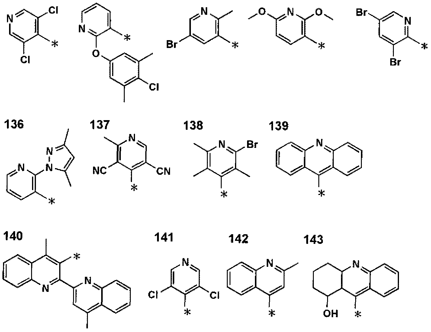
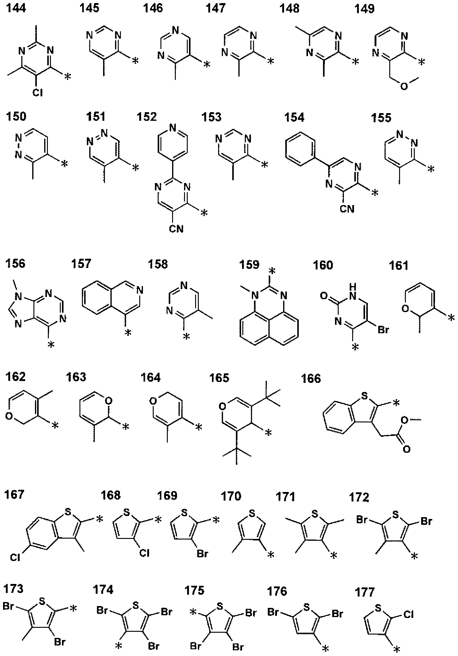
[0093] [化 12]

[0094] [化 13]

[0095] [化 14]

[0096] [化 15]
 00Zdf/13d LZ 6ίΊ.60/.00Ζ ΟΛ\

[0098] [化 17]

[0099] [化 18]

[0100] [化 19]

[0101] [化 20]
388 389 390 391

[0102] 一般式(1)において、 Yは炭素原子または窒素原子を表し、好ましくは炭素原子で ある。 Bは C (R ) =C (R ) 、 一 N = C (R ) 、 一 C (R ) =N または N = N
01 02 02 01
を表す。
[0103] 一般式(1)において、 Yを含む含窒素複素環基の好ましい例としては、 2 イミダゾ リル基、 2— (1, 3, 4 トリァゾリル)基、 2— (1, 3, 5 トリァゾリル)基、 2—テトラゾリ ル基等が挙げられる。これらの含窒素複素環基で最も好ましくは 2—イミダゾリル基で ある。
[0104] 一般式(1)において、 R 及び R は水素原子または置換基を表す。置換基の例と
01 02
してはアルキル基(例えば、メチル基、ェチル基、プロピル基、イソプロピル基、 tert ブチル基、ペンチル基、へキシル基、ォクチル基、ドデシル基、トリデシル基、テト ラデシル基、ペンタデシル基等)、シクロアルキル基 (例えば、シクロペンチル基、シク 口へキシル基等)、アルケニル基 (例えば、ビニル基、ァリル基等)、アルキニル基 (例 えば、ェチュル基、プロパルギル基等)、芳香族炭化水素環基 (芳香族炭素環基、ァ リール基等ともいい、例えば、フエ-ル基、 p—クロ口フエ二ル基、メシチル基、トリル基 、キシリル基、ナフチル基、アントリル基、ァズレニル基、ァセナフテニル基、フルォレ -ル基、フエナントリル基、インデュル基、ピレニル基、ビフエ-リル基等)、芳香族複 素環基 (例えば、ピリジル基、ピリミジニル基、フリル基、ピロリル基、イミダゾリル基、ベ ンゾイミダゾリル基、ピラゾリル基、ピラジュル基、トリァゾリル基 (例えば、 1, 2, 4 トリ ァゾールー 1ーィル基、 1, 2, 3 トリァゾールー 1 ィル基等)、ォキサゾリル基、ベ
ンゾォキサゾリル基、チアゾリル基、イソォキサゾリル基、イソチアゾリル基、フラザニル 基、チェ-ル基、キノリル基、ベンゾフリル基、ジベンゾフリル基、ベンゾチェ-ル基、 ジベンゾチェ-ル基、インドリル基、カルバゾリル基、カルボリニル基、ジァザ力ルバ ゾリル基 (前記カルボリ-ル基のカルボリン環を構成する炭素原子の一つが窒素原 子で置き換わったものを示す)、キノキサリニル基、ピリダジ -ル基、トリアジ-ル基、 キナゾリニル基、フタラジュル基等)、複素環基 (例えば、ピロリジル基、イミダゾリジル 基、モルホリル基、ォキサゾリジル基等)、アルコキシ基 (例えば、メトキシ基、エトキシ 基、プロピルォキシ基、ペンチルォキシ基、へキシルォキシ基、ォクチルォキシ基、ド デシルォキシ基等)、シクロアルコキシ基 (例えば、シクロペンチルォキシ基、シクロへ キシルォキシ基等)、ァリールォキシ基 (例えば、フエノキシ基、ナフチルォキシ基等) 、アルキルチオ基(例えば、メチルチオ基、ェチルチオ基、プロピルチオ基、ペンチル チォ基、へキシルチオ基、ォクチルチオ基、ドデシルチオ基等)、シクロアルキルチオ 基 (例えば、シクロペンチルチオ基、シクロへキシルチオ基等)、ァリールチオ基 (例え ば、フエ-ルチオ基、ナフチルチオ基等)、アルコキシカルボ-ル基 (例えば、メチル ォキシカルボニル基、ェチルォキシカルボニル基、ブチルォキシカルボニル基、オタ チルォキシカルボ-ル基、ドデシルォキシカルボ-ル基等)、ァリールォキシカルボ -ル基(例えば、フエ-ルォキシカルボ-ル基、ナフチルォキシカルボ-ル基等)、ス ルファモイル基(例えば、アミノスルホ -ル基、メチルアミノスルホ -ル基、ジメチルアミ ノスルホ -ル基、ブチルアミノスルホ -ル基、へキシルアミノスルホ -ル基、シクロへキ シルアミノスルホ -ル基、ォクチルアミノスルホ -ル基、ドデシルアミノスルホ-ル基、 フエ-ルアミノスルホ -ル基、ナフチルアミノスルホ -ル基、 2—ピリジルアミノスルホ- ル基等)、ァシル基(例えば、ァセチル基、ェチルカルボ-ル基、プロピルカルボ-ル 基、ペンチルカルボ-ル基、シクロへキシルカルボ-ル基、ォクチルカルポ-ル基、 2 ェチルへキシルカルボ-ル基、ドデシルカルポ-ル基、フエ-ルカルポ-ル基、ナ フチルカルボニル基、ピリジルカルボニル基等)、ァシルォキシ基 (例えば、ァセチル ォキシ基、ェチルカルボニルォキシ基、ブチルカルボニルォキシ基、ォクチルカルボ -ルォキシ基、ドデシルカルボ-ルォキシ基、フエ-ルカルポ-ルォキシ基等)、アミ ド基(例えば、メチルカルボ-ルァミノ基、ェチルカルボ-ルァミノ基、ジメチルカルボ
-ルァミノ基、プロピルカルボ-ルァミノ基、ペンチルカルボ-ルァミノ基、シクロへキ シルカルボ-ルァミノ基、 2—ェチルへキシルカルボ-ルァミノ基、ォクチルカルボ- ルァミノ基、ドデシルカルポ-ルァミノ基、フエ-ルカルポ-ルァミノ基、ナフチルカル ボニルァミノ基等)、力ルバモイル基 (例えば、ァミノカルボ-ル基、メチルァミノカルボ -ル基、ジメチルァミノカルボ-ル基、プロピルアミノカルボ-ル基、ペンチルァミノ力 ルポ-ル基、シクロへキシルァミノカルボ-ル基、ォクチルァミノカルボ-ル基、 2—ェ チルへキシルァミノカルボ-ル基、ドデシルァミノカルボ-ル基、フエ-ルァミノカルボ -ル基、ナフチルァミノカルボ-ル基、 2—ピリジルァミノカルボニル基等)、ウレイド基 (例えば、メチルウレイド基、ェチルウレイド基、ペンチルゥレイド基、シクロへキシルゥ レイド基、ォクチルゥレイド基、ドデシルウレイド基、フ ニルウレイド基ナフチルゥレイ ド基、 2—ピリジルアミノウレイド基等)、スルフィエル基 (例えば、メチルスルフィエル基 、ェチルスルフィ-ル基、ブチルスルフィ-ル基、シクロへキシルスルフィ-ル基、 2— ェチルへキシルスルフィ-ル基、ドデシルスルフィ-ル基、フエ-ルスルフィ-ル基、 ナフチルスルフィエル基、 2—ピリジルスルフィエル基等)、アルキルスルホ -ル基(例 えば、メチルスルホ -ル基、ェチルスルホ -ル基、ブチルスルホ -ル基、シクロへキシ ルスルホ-ル基、 2—ェチルへキシルスルホ -ル基、ドデシルスルホ -ル基等)、ァリ 一ルスルホ -ル基またはへテロアリールスルホ -ル基(例えば、フエ-ルスルホ-ル 基、ナフチルスルホニル基、 2—ピリジルスルホニル基等)、アミノ基 (例えば、アミノ基 、ェチルァミノ基、ジメチルァミノ基、ブチルァミノ基、シクロペンチルァミノ基、 2—ェ チルへキシルァミノ基、ドデシルァミノ基、ァ-リノ基、ナフチルァミノ基、 2—ピリジル アミノ基等)、ハロゲン原子 (例えば、フッ素原子、塩素原子、臭素原子等)、フッ化炭 化水素基(例えば、フルォロメチル基、トリフルォロメチル基、ペンタフルォロェチル 基、ペンタフルオロフェ-ル基等)、シァノ基、ニトロ基、ヒドロキシ基、メルカプト基、シ リル基 (例えば、トリメチルシリル基、トリイソプロビルシリル基、トリフエ-ルシリル基、フ ェニルジェチルシリル基等)等が挙げられる。これらの置換基は上記の置換基によつ て更に置換されていてもよい。また、これらの置換基は複数が互いに結合して環を形 成していてもよい。
一般式(1)の A— C Xで表される炭化水素環基または複素環基において、 Xは炭
素原子または窒素原子を表し、好ましくは炭素原子である。
[0106] A— C Xで表される炭化水素環基が芳香族炭化水素環基のとき、 (4η+ 2) π系 の芳香族炭化水素化合物から任意の位置の水素原子を 1つ取り除いたものであり、 具体的にはフエニル基、 1—ナフチル基、 2 ナフチル基、 9 アントリル基、 1—アン トリル基、 9 フエナントリル基、 2 トリフエ-レニル基、 3 ペリレニル基等が挙げら れる。
[0107] 更に該炭化水素環基は、例えば、一般式(1)において、 R で表される置換基によ
011
つて置換されていてもよぐ更に縮合環 (例えば、 9 フエナントリル基に炭化水素環 を縮合させた 9ーピレニル基、フエ-ル基に複素環を縮合させた 8—キノリル基等)を 形成してちょい。
[0108] Α— C Xで表される複素環基が芳香族複素環基のとき、該芳香族複素環基は含 窒素芳香族複素環に結合する部分の少なくとも片隣接位が炭素原子であり、且つ、 ( 4η+ 2) π系の芳香族基であれば特に制限はないが、含窒素芳香族複素環に結合 する部分の両隣接位が炭素原子であることが好ましい。
[0109] 具体的には、 3 ピリジル基、 5 ピリミジル基、 4 ピリダジル基、 5 ピリダジル基 、 4 イソォキサゾリル基、 4 イソチアゾリル基、 4 ピラゾリル基、 3—ピロ口基、 3— フリル基、 3—チェニル基等が挙げられる。更に該複素環は、例えば、 R で説明した
01 置換基によって置換されて 、てもよく、更に縮合環を形成してもよ 、。
[0110] 一般式(1)において、 X— LI— Xは 2座の配位子を表し、 X、 Xは各々独立に炭
1 2 1 2
素原子、窒素原子または酸素原子を表す。 L1は X、 Xと共に 2座の配位子を形成す
1 2
る原子群を表す。 X -L1 -Xで表される 2座の配位子の具体例としては、置換また
1 2
は無置換のフエニルピリジン、フエ-ルビラゾール、フエ-ルイミダゾール、フエ-ルト リアゾール、フエ-ルテトラゾール、ビラザボール、ァセチルアセトン、ピコリン酸等が 挙げられる。 mlは 1、 2または 3の整数を表し、 m2は 0、 1または 2の整数を表すが、 ml +m2は 2または 3である。中でも、 m2は 0である場合が好ましい。
[0111] 一般式(2)において、 Rはイミダゾール環の窒素原子に結合する Z力もなる環のォ
2
ルト位に位置する立体パラメーター値 (Es値)がー 0. 5以下の置換基を表す。 Es値 の詳細な説明は一般式(1)で示したものと同義であり。 Rの具体的な例は一般式(1)
の説明における表 1に示した置換基が挙げられる。
[0112] Rは水素原子または置換基を表し、 nlは 1から 4の整数を表す。 Rは水素原子ま
1 2
たは置換基を表し、 n2は 1から 2の整数を表す。
[0113] 一般式 (2)において、 Zは炭化水素環または複素環、またはその互変異性体を形
2
成するのに必要な原子群を表す。
[0114] 一般式 (2)において、 Zで表される炭化水素環としては、非芳香族炭化水素環、芳
2
香族炭化水素環が挙げられ、非芳香族炭化水素環としては、シクロプロパン環、シク 口ペンタン環、シクロへキサン環等が挙げられる。
[0115] これらの環は無置換でも置換基を有していても良ぐ該置換基としては、一般式(1) において R 、R で各々表されるは置換基が挙げられる。
01 02
[0116] また、芳香族炭化水素環 (芳香族炭素環、ァリール環等ともいう)としては、ベンゼン 環、ビフエ-ル環、ナフタレン環、ァズレン環、アントラセン環、フエナントレン環、ピレ ン環、タリセン環、ナフタセン環、トリフエ-レン環、 o—テルフエ-ル環、 m—テルフエ -ル環、 p—テルフエ-ル環、ァセナフテン環、コロネン環、フルオレン環、フルオラン トレン環、ナフタセン環、ペンタセン環、ペリレン環、ペンタフェン環、ピセン環、ピレン 環、ピラントレン環、アンスラアントレン環等が挙げられる。
[0117] これらの環は無置換でも置換基を有していても良ぐ該置換基としては、一般式(1) において R 、R で各々表されるは置換基が挙げられる。
01 02
[0118] 一般式 (2)において、 Zで表される複素環としては、非芳香族複素環、芳香族複素
2
環が挙げられ、非芳香族複素環としては、例えば、エポキシ環、アジリジン環、チイラ ン環、ォキセタン環、ァゼチジン環、チェタン環、テトラヒドロフラン環、ジォキソラン環 、ピロリジン環、ビラゾリジン環、イミダゾリジン環、ォキサゾリジン環、テトラヒドロチオフ ェン環、スノレホラン環、チアゾリジン環、 ε一力プロラタトン環、 ε—力プロラタタム環、 ピぺリジン環、へキサヒドロピリダジン環、へキサヒドロピリミジン環、ピぺラジン環、モ ルホリン環、テトラヒドロピラン環、 1, 3 ジォキサン環、 1, 4 ジォキサン環、トリオキ サン環、テトラヒドロチォピラン環、チオモルホリン環、チォモノレホリン 1、 1 ジォキ シド環、ビラノース環、ジァザビシクロ [2, 2, 2]—オクタン環等が挙げられる。これら の環は、無置換でも置換基を有していても良ぐ該置換基としては、一般式(1)にお
いて R 、R で各々表されるは置換基が挙げられる。
01 02
[0119] 一般式(2)にお 、て、 Zで表される芳香族複素環としては、フラン環、チォフェン環
2
、ォキサゾール環、ピロール環、ピリジン環、ピリダジン環、ピリミジン環、ピラジン環、 トリアジン環、ベンゾイミダゾール環、ォキサジァゾール環、トリァゾール環、イミダゾー ル環、ピラゾール環、チアゾール環、インドール環、ベンゾイミダゾール環、ベンゾチ ァゾール環、ベンゾォキサゾール環、キノキサリン環、キナゾリン環、フタラジン環、力 ルバゾール環、カルボリン環、ジァザ力ルバゾール環(カルボリン環を構成する炭化 水素環の炭素原子の一つが更に窒素原子で置換されている環を示す)等が挙げら れる。これらの環は、無置換でも置換基を有していても良ぐ該置換基としては、一般 式(1)において R 、R で各々表される置換基が挙げられる。
01 02
[0120] 更に複数の置換基が存在する場合、その複数の置換基は連結して環を形成しても よい。好ましい具体例は、一般式(1)の Zで挙げられた基である。
[0121] 一般式(2)において、 Zは C Cと共に 5〜6員の、 2価の炭化水素環基または 2価
1
の複素環基を形成するのに必要な原子群を表す。 2価の炭化水素環基としては 2価 の芳香族炭化水素環基が好ましぐ 2価の複素環基としては 2価の芳香族複素環基 が好ましい。
[0122] 2価の芳香族炭化水素環基は、 (4η+ 2) π系の芳香族炭化水素化合物から任意 の位置の水素原子を 2つ取り除いたものであり、具体的には、ベンゼン環、ナフタレン 環、アントラセン環、フエナントレン環、トリフエ-レン環、ペリレン環等力 導出される 2 価の基が挙げられる。
[0123] 上記の 2価の芳香族炭化水素環基は、更に、一般式(1)の R で説明した置換基に
01
よって置換されて 、てもよく、更に縮合環を形成してもよ 、。
[0124] 2価の芳香族複素環基は、含窒素芳香族複素環に結合する部分の少なくとも片隣 接位が炭素原子であり、且つ (4η+ 2) π系の芳香族基であれば特に制限はないが 、含窒素芳香族複素環に結合する部分の両隣接位が炭素原子であることが好ましい
[0125] 2価の芳香族複素環基としては、具体的には、ピリジン環、ピリミジン環、ピリダジン 環、イソォキサゾール環、イソチアゾール環、ピラゾール環、ピロール環、フラン環、チ
オフ ン環等力 導出される 2価の基が挙げられる。
[0126] 上記の 2価の芳香族複素環基は、更に、一般式(1)の R で説明した置換基によつ
01
て置換されていてもよぐ更に縮合環を形成してもよい。
[0127] 一般式(2)において、 R及び Rは水素原子または置換基を表し、 nlは 1から 4、 n2
1 2
は 1から 2の整数を表す。
[0128] 一般式(2)において、 R及び Rで表される置換基としては、一般式(1)において、
1 2
R 、R
01 02で各々表される置換基と同義である。
[0129] 但し、複数の置換基が Rまたは Rに存在する場合、それぞれの Rまたは Rは同一
1 2 1 2 であってもよぐまた異なっていてもよい。更に Rまたは Rの複数の置換基はお互い
1 2
に結合して環を形成してもよ 、。
[0130] 一般式(2)において、 X -L1 -Xは 2座の配位子を表し、 X、 Xは各々独立に炭
1 2 1 2
素原子、窒素原子または酸素原子を表す。 L1は X、 X
1 2と共に 2座の配位子を形成す る原子群を表す。 X -L1 -Xで表される 2座の配位子の具体例としては、置換また
1 2
は無置換のフエニルピリジン、フエ-ルビラゾール、フエ-ルイミダゾール、フエ-ルト リアゾール、フエ-ルテトラゾール、ビラザボール、ァセチルアセトン、ピコリン酸等が 挙げられる。 mlは 1、 2または 3の整数を表し、 m2は 0、 1または 2の整数を表すが、 ml +m2は 2または 3である。中でも、 m2は 0である場合が好ましい。
[0131] 一般式(3)において、 Rは立体パラメーター値 (Es値)がー 0. 5以下の置換基を表 す。 Es値の詳細な説明は一般式(1)で示したものと同義であり。 Rの具体的な例は 一般式(1)の説明における表 1に示した置換基が挙げられる。
[0132] R及び Rは水素原子または置換基を表し、一般式(2)における記載と同義である。
1 2
Rは水素原子または置換基を表し、 n3は 1から 4の整数を表す。但し、複数の置換
3
基 Rが存在する場合、それぞれの Rは同一であってもよぐまた異なっていてもよい
3 3
。更に複数の Rはお互いに結合して環を形成してもよい。
3
[0133] 一般式(3)において、 X -L1 -Xは 2座の配位子を表し、 X、 Xは各々独立に炭
1 2 1 2
素原子、窒素原子または酸素原子を表す。 L1は X、 Xと共に 2座の配位子を形成す
1 2
る原子群を表す。 X -L1 -Xで表される 2座の配位子の具体例としては、一般式(2
1 2
)の記載と同義である。 mlは 1、 2または 3の整数を表し、 m2は 0、 1または 2の整数を
表すが、 ml +m2は 2または 3である。中でも、 m2は 0である場合が好ましい。
[0134] 一般式 (4)において、 R及び R' は立体パラメーター値 (Es値)がー 0. 5以下の置 換基を表す。 Es値の詳細な説明は一般式(1)で示したものと同義であり。 R及び の具体的な例は一般式(1)の説明における表 1に示した置換基が挙げられる。
[0135] R及び Rは水素原子または置換基を表し、一般式(2)における記載と同義である。
1 2
Rは水素原子または置換基を表し、 n3は 1から 4の整数を表す。但し、複数の置換
3
基 Rが存在する場合、それぞれの Rは同一であってもよぐまた異なっていてもよい
3 3
。更に複数の Rはお互いに結合して環を形成してもよい。
3
[0136] 一般式 (4)において、 X -L1 -Xは 2座の配位子を表し、 X、 Xは各々独立に炭
1 2 1 2
素原子、窒素原子または酸素原子を表す。 L1は X、 Xと共に 2座の配位子を形成す
1 2
る原子群を表す。 X -L1 -Xで表される 2座の配位子の具体例としては、一般式(2
1 2
)の記載と同義である。 mlは 1、 2または 3の整数を表し、 m2は 0、 1または 2の整数を 表すが、 ml +m2は 2または 3である。中でも、 m2は 0である場合が好ましい。
[0137] 一般式(2)〜 (4)にお 、て、 R及び は電子供与性基であることが好ま 、。電 子供与性基の説明は、一般式(1)における電子供与性基の説明と同義である。
[0138] 以下、本発明に係る前記一般式(1)、(2)、(3)または一般式 (4)で表される金属 錯体の具体例を示すが、本発明はこれらに限定されない。
[0139] [化 21]
\_ZZ \ [0 ]


[0141] [化 23]
z \ [mo]

(21) v)
0.60SO/.OOZdf/X3d zv 6M.60/.00Z OAV

[0143] [化 25]
[9 ] [漏]

0.60S0/.00Zdf/X3d 6M.60/.00Z OAV
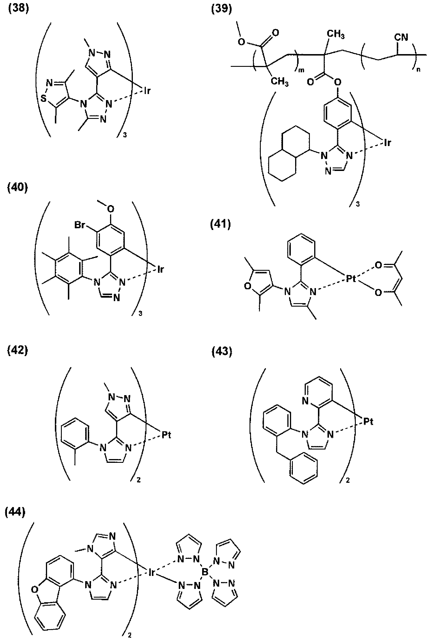
[0145] [化 27]

[0146] [化 28]

[0147] [化 29]

[0148] [化 30]
m [6wo]

0.60S0/.00Zdf/X3d 617 6M.60/.00Z OAV

[0150] [化 32]

[0151] [化 33]
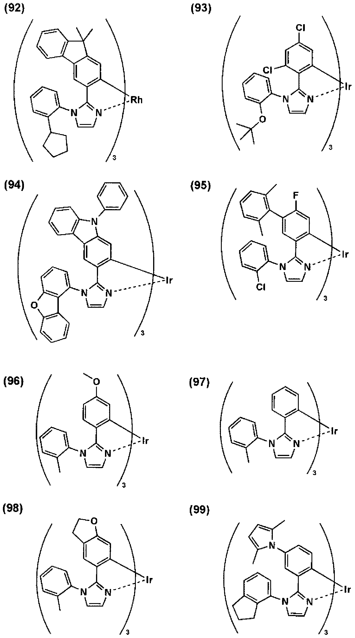
[0152] [化 34]


[0154] [化 36]

[0155] [化 37]

[0156] [化 38]
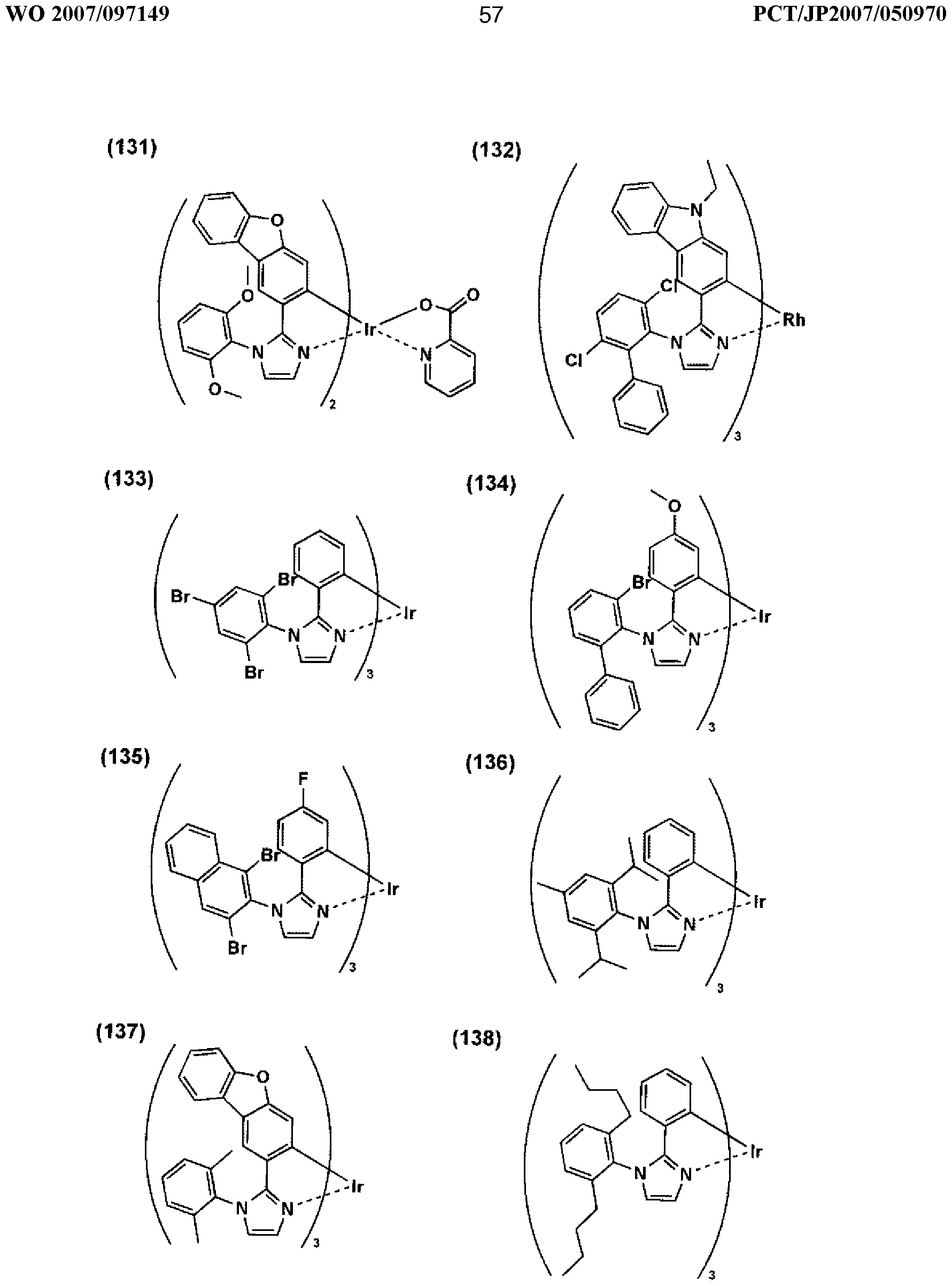
[0157] [化 39]

[0158] [化 40]
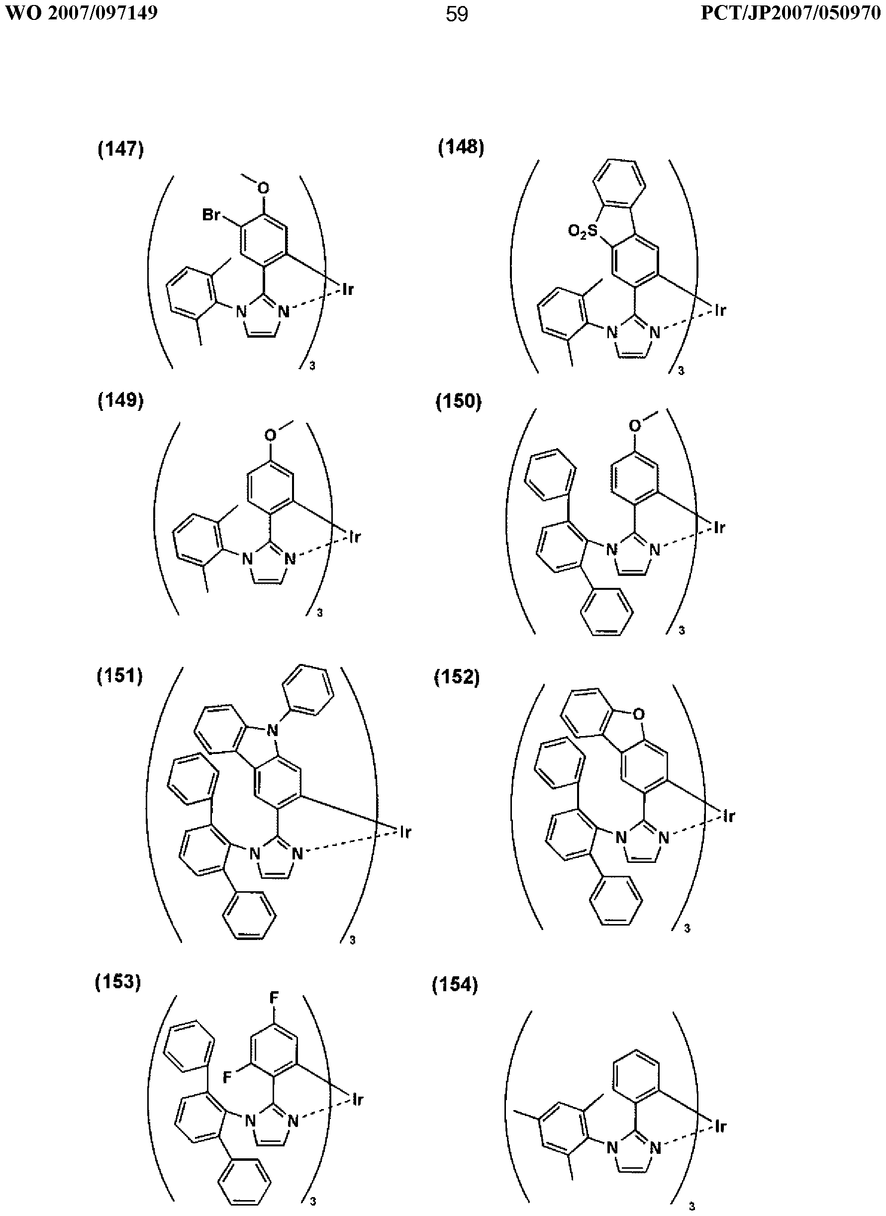
[0159] [化 41]
[0910]


[0161] [化 43]

[0162] [化 44]

[0163] [化 45]

[0164] これらの金属錯体は、例えば、 Organic Letter誌、 vol3、 No. 16、 2579〜258 1頁(2001)、 Inorganic Chemistry,第 30卷、第 8号、 1685〜1687頁(1991年
J. Am. Chem. Soc. , 123卷、 4304頁(2001年)、 Inorganic Chemistry, 第 40卷、第 7号、 1704〜1711頁(2001年)、 Inorganic Chemistry,第 41卷、 第 12号、 3055〜3066頁(2002年)、 New Journal of Chemistry. ,第 26卷、 1171頁(2002年)、 European Journal of Organic Chemistry,第 4卷、 695 〜709頁(2004年)、更にこれらの文献中に記載の参考文献等の方法を適用するこ とにより合成できる。
[0165] 以下に、代表的な化合物の合成例を示す。
[0166] 例示化合物(154)の合成
[0167] [化 46]

[0170] 溶媒を減圧濃縮した後に得られた固体に水 1Lを加えて懸濁後、固体を濾取した。
得られた結晶を更にメタノール/水 = 1/1混合溶液で洗浄し、乾燥後 14. 7g (収率 93. 6%)の錯体 Bを得た。
[0171] 窒素雰囲気下で錯体 B、 7. 5g (0. 009214モル)及び 2—フエ-ルー (2, 4, 6—ト リメチルフエ-ル)— 1H—イミダゾール、 6. 0g (0. 02287モル)をグリセリン 400ml に懸濁させた。窒素雰囲気下で反応温度 150°C〜160°Cの間で 2時間反応させ、錯 体 Bの消失を確認したところで反応終了とした。反応液を冷却し、メタノール 500mlを 加え、析出した結晶を濾取した。得られた結晶を更にメタノールで洗浄し、乾燥後収 量 7. lg (収率 78. 9%)の粗生成物を得た。この粗生成物を少量の塩化メチレンに 溶解し、シカゲルカラムクロマトグラフィーによって精製し (塩化メチレン) 6. 5g (収率 72. 2%)の例示化合物(154)を得た。
[0172] 日立製作所製 F— 4500を用いて測定した例示化合物(154)の溶液におけるリン 光発光波長は、 466nmであった(2—メチルテトラヒドロフラン中)。
[0173] 《有機 EL素子材料の有機 EL素子への適用》
本発明の有機 EL素子を作製する場合、有機 EL素子の構成層 (詳細は後述する) の中で、発光層または電子阻止層に本発明に係る上記一般式(1)〜 (4)の 、ずれ 力 1種で表される金属錯体を用いることが好ましい。また、発光層中では上記のように 発光ドーパントとして好ましく用いられる。
[0174] (発光ホストと発光ドーパント)
発光層中の主成分であるホストイ匕合物である発光ホストに対する発光ドーパントとの 混合比は、好ましくは質量で 0. 1質量%〜30質量%未満の範囲に調整することであ る。
[0175] 但し、発光ドーパントは複数種の化合物を混合して用いてもよぐ混合する相手は 構造を異にする、その他の金属錯体やその他の構造を有するリン光性ドーパントや
蛍光性ドーパントでもよい。
[0176] ここで、発光ドーパントとして用いられる金属錯体と併用してもよいドーパント(リン光 性ドーパント、蛍光性ドーパント等)について述べる。発光ドーパントは大きく分けて、 蛍光を発光する蛍光性ドーパントとリン光を発光するリン光性ドーパントの 2種類があ る。
[0177] 前者 (蛍光性ドーパント)の代表例としては、クマリン系色素、ピラン系色素、シ了ニ ン系色素、クロコニゥム系色素、スクァリウム系色素、ォキソベンツアントラセン系色素 、フルォレセイン系色素、ローダミン系色素、ピリリウム系色素、ペリレン系色素、スチ ルベン系色素、ポリチォフェン系色素、または希土類錯体系蛍光体等が挙げられる。
[0178] 後者 (リン光性ドーパント)の代表例としては、好ましくは元素周期表で 8族、 9族、 1 0族の遷移金属元素を含有する錯体系化合物であり、更に好ましくはイリジウム化合 物、オスミウム化合物であり、中でも最も好ましいのはイリジウム化合物である。
[0179] 具体的には以下の特許公報に記載されている化合物である。
[0180] 国際公開第 OOZ70655号パンフレツ K特開 2002— 280178号公報、特開 2001
— 181616号公報、特開 2002— 280179号公報、特開 2001— 181617号公報、 特開 2002— 280180号公報、特開 2001— 247859号公報、特開 2002— 299060 号公報、特開 2001— 313178号公報、特開 2002— 302671号公報、特開 2001— 345183号公報、特開 2002— 324679号公報、国際公開第 02,15645号パンフ レッド、特開 2002— 332291号公報、特開 2002— 50484号公報、特開 2002— 33 2292号公報、特開 2002— 83684号公報、特表 2002— 540572号公報、特開 20 02— 117978号公報、特開 2002— 338588号公報、特開 2002— 170684号公報 、特開 2002— 352960号公報、国際公開第 01/93642号パンフレット、特開 2002
— 50483号公報、特開 2002— 100476号公報、特開 2002— 173674号公報、特 開 2002— 359082号公報、特開 2002— 175884号公報、特開 2002— 363552号 公報、特開 2002— 184582号公報、特開 2003— 7469号公報、特表 2002— 525 808号公報、特開 2003— 7471号公報、特表 2002— 525833号公報、特開 2003
— 31366号公報、特開 2002— 226495号公報、特開 2002— 234894号公報、特 開 2002— 235076号公報、特開 2002— 241751号公報、特開 2001— 319779号
公報、特開 2001— 319780号公報、特開 2002— 62824号公報、特開 2002— 10 0474号公報、特開 2002— 203679号公報、特開 2002— 343572号公報、特開 2 002— 203678号公報等。
[0181] 以下に、具体例の一部を示す。
[0182] [化 47]
Pt- 1 Pt-2

[0183] [化 48]
lr-1 ir-2

I 一: lr-8

lr-9 lr-10

!r一 11 lr— 12

Ir一 13

[0185] (発光ホスト)
本発明に用いられるホストイ匕合物とは、発光層に含有される化合物のうちで室温(2 5°C)においてリン光発光のリン光量子収率が、 0. 01未満の化合物を表す。
[0186] 本発明に用いられる発光ホストとしては構造的には特に制限はないが、代表的に は力ルバゾール誘導体、トリアリールァミン誘導体、芳香族ボラン誘導体、含窒素複 素環化合物、チォフェン誘導体、フラン誘導体、オリゴァリーレンィ匕合物等の基本骨
格を有するもの、またはカルボリン誘導体ゃ該カルボリン誘導体のカルボリン環を構 成する炭化水素環の炭素原子の少なくとも一つが窒素原子で置換されている環構 造を有する誘導体等が挙げられる。中でも、力ルバゾール誘導体、カルボリン誘導体 ゃ該カルボリン誘導体のカルボリン環を構成する炭化水素環の炭素原子の少なくと も一つが窒素原子で置換されている環構造を有する誘導体が好ましく用いられる。
[0187] 以下に具体例を挙げるが、本発明はこれらに限定されない。これらの化合物は正孔 阻止材料として使用することも好ま ヽ。
[0188] [化 50]
[TS ] [6810]


.60S0/.00Zdf/X3d ε 6M.60/.00Z OAV

[0191] [化 53]
H23 H24

[0192] 本発明に係る発光層にお ヽては、ホストイ匕合物として公知のホストイ匕合物を複数種 併用して用いてもよい。ホストイ匕合物を複数種用いることで、電荷の移動を調整する ことが可能であり、有機 EL素子を高効率ィ匕することができる。これらの公知のホストイ匕 合物としては、正孔輸送能、電子輸送能を有しつつ、発光の長波長化を防ぎ、且つ 、高 Tg (ガラス転移温度)である化合物が好ましい。
[0193] また、本発明に用いられる発光ホストは低分子化合物でも、繰り返し単位をもつ高 分子化合物でもよぐビニル基やエポキシ基のような重合性基を有する低分子化合 物 (蒸着重合性発光ホスト)でも 、 、。
[0194] 発光ホストとしては、正孔輸送能、電子輸送能を有しつつ、且つ発光の長波長化を 防ぎ、なお且つ高 Tg (ガラス転移温度)である化合物が好ま 、。
[0195] 発光ホストの具体例としては、以下の文献に記載されている化合物が好適である。
例えば、特開 2001— 257076号公報、特開 2002— 308855号公報、特開 2001— 313179号公報、特開 2002— 319491号公報、特開 2001— 357977号公報、特 開 2002— 334786号公報、特開 2002— 8860号公報、特開 2002— 334787号公 報、特開 2002— 15871号公報、特開 2002— 334788号公報、特開 2002— 4305 6号公報、特開 2002— 33 9号公報、特開 2002— 75645号公報、特開 2002— 338579号公報、特開 2002— 105445号公報、特開 2002— 343568号公報、特 開 2002— 141173号公報、特開 2002— 352957号公報、特開 2002— 203683号 公報、特開 2002— 363227号公報、特開 2002— 231453号公報、特開 2003— 3 165号公報、特開 2002— 234888号公報、特開 2003— 27048号公報、特開 200 2— 255934号公報、特開 2002— 260861号公報、特開 2002— 280183号公報、 特開 2002— 299060号公報、特開 2002— 302516号公報、特開 2002— 305083 号公報、特開 2002— 305084号公報、特開 2002— 308837号公報等。
[0196] また、発光層はホストイ匕合物として更に蛍光極大波長を有するホストイ匕合物を含有 していてもよい。この場合、他のホスト化合物とリン光性化合物から蛍光性化合物へ のエネルギー移動で、有機 EL素子としての電界発光は蛍光極大波長を有する他の ホストィヒ合物からの発光も得られる。蛍光極大波長を有するホストィヒ合物として好まし いのは、溶液状態で蛍光量子収率が高いものである。ここで、蛍光量子収率は 10% 以上、特に 30%以上が好ましい。具体的な蛍光極大波長を有するホスト化合物とし ては、クマリン系色素、ピラン系色素、シァニン系色素、クロコニゥム系色素、スクァリ ゥム系色素、ォキソベンツアントラセン系色素、フルォレセイン系色素、ローダミン系 色素、ピリリウム系色素、ペリレン系色素、スチルベン系色素、ポリチォフェン系色素 等が挙げられる。蛍光量子収率は、前記第 4版実験化学講座 7の分光 IIの 362頁(1 992年版、丸善)に記載の方法により測定することができる。
[0197] 次に、代表的な有機 EL素子の構成について述べる。
[0198] 《有機 EL素子の構成層》
本発明の有機 EL素子の構成層につ 、て説明する。
[0199] 本発明の有機 EL素子の層構成の好ましい具体例を以下に示すが、本発明はこれ らに限定されない。
[0200] (i)陽極 Z正孔輸送層 Z発光層 Z正孔阻止層 Z電子輸送層 Z陰極
(ii)陽極 Z電子阻止層 Z発光層 Z正孔阻止層 Z電子輸送層 Z陰極
(m)陽極 Z正孔輸送層 Z電子阻止層 Z発光層 Z正孔阻止層 Z電子輸送層 Z陰 極
(iv)陽極 Z正孔輸送層 Z電子阻止層 Z発光層 Z正孔阻止層 Z電子輸送層 Z陰 極
(V)陽極 Z正孔輸送層 Z電子阻止層 Z発光層 Z正孔阻止層 Z電子輸送層 Z陰 極バッファ一層 z陰極
(vi)陽極 Z陽極バッファ一層 Z正孔輸送層 Z電子阻止層 Z発光層 Z正孔阻止層 Z電子輸送層 Z陰極バッファ一層 Z陰極
(vii)陽極 Z陽極バッファ一層 Z正孔輸送層 Z電子阻止層 Z発光層 Z正孔阻止層 Z電子輸送層 Z陰極バッファ一層 Z陰極
《阻止層 (電子阻止層、正孔阻止層)》
本発明に係る阻止層(例えば、電子阻止層、正孔阻止層)について説明する。
[0201] 本発明においては、正孔阻止層、電子阻止層等に本発明の有機 EL素子材料を用 V、ることが好ましぐ特に好ましくは正孔阻止層に用いることである。
[0202] 本発明の有機 EL素子材料を正孔阻止層、電子阻止層に含有させる場合、請求の 範囲第 1項〜請求の範囲第 7項のいずれか 1項に記載されている本発明の有機 EL 素子材料を、正孔阻止層や電子阻止層等の層構成成分として 100質量%の状態で 含有させてもよいし、他の有機化合物等と混合してもよい。
[0203] 本発明に係る阻止層の膜厚としては好ましくは 3ηπ!〜 lOOnmであり、更に好ましく ίま 5nm〜30nmでめる。
[0204] 《正孔阻止層》
正孔阻止層とは広い意味では電子輸送層の機能を有し、電子を輸送する機能を有 しつつ正孔を輸送する能力が著しく小さい材料力 なり、電子を輸送しつつ正孔を阻
止することで電子と正孔の再結合確率を向上させることができる。
[0205] 正孔阻止層としては、例えば、特開平 11 204258号公報、同 11 204359号公 報、及び「有機 EL素子とその工業化最前線(1998年 11月 30日 ェヌ'ティー 'エス 社発行)」の 237頁等に記載の正孔阻止(ホールブロック)層等を本発明に係る正孔 阻止層として適用可能である。また、後述する電子輸送層の構成を必要に応じて、本 発明に係る正孔阻止層として用いることができる。
[0206] 本発明の有機 EL素子は構成層として正孔阻止層を有し、該正孔阻止層が前記力 ルポリン誘導体または該カルボリン誘導体のカルボリン環を構成する炭化水素環の 炭素原子の少なくとも一つが窒素原子で置換されている環構造を有する誘導体を含 有することが好ましい。
[0207] 《電子阻止層》
一方、電子阻止層とは広い意味では正孔輸送層の機能を有し、正孔を輸送する機 能を有しつつ電子を輸送する能力が著しく小さい材料力 なり、正孔を輸送しつつ電 子を阻止することで電子と正孔の再結合確率を向上させることができる。また、後述 する正孔輸送層の構成を必要に応じて電子阻止層として用いることができる。
[0208] また、本発明においては、発光層に隣接する隣接層、即ち正孔阻止層、電子阻止 層に上記の本発明の有機 EL素子材料を用いることが好ましぐ特に電子阻止層に 用いることが好ましい。
[0209] 《正孔輸送層》
正孔輸送層とは正孔を輸送する機能を有する材料を含み、広い意味で正孔注入 層、電子阻止層も正孔輸送層に含まれる。正孔輸送層は単層もしくは複数層設ける ことができる。
[0210] 正孔輸送材料としては、特に制限はなぐ従来、光導伝材料において正孔の電荷 注入輸送材料として慣用されているものや、有機 EL素子の正孔注入層、正孔輸送 層に使用される公知のものの中から任意のものを選択して用いることができる。
[0211] 正孔輸送材料は正孔の注入もしくは輸送、電子の障壁性のいずれかを有するもの であり、有機物、無機物のいずれであってもよい。例えば、トリァゾール誘導体、ォキ サジァゾール誘導体、イミダゾール誘導体、ポリアリールアルカン誘導体、ピラゾリン
誘導体及びピラゾロン誘導体、フ 二レンジァミン誘導体、ァリールァミン誘導体、アミ ノ置換カルコン誘導体、ォキサゾール誘導体、スチリルアントラセン誘導体、フルォレ ノン誘導体、ヒドラゾン誘導体、スチルベン誘導体、シラザン誘導体、ァニリン系共重 合体、また導電性高分子オリゴマー、特にチォフェンオリゴマー等が挙げられる。
[0212] 正孔輸送材料としては上記のものを使用することができる力 ボルフイリンィ匕合物、 芳香族第三級ァミン化合物及びスチリルアミン化合物、特に、芳香族第三級ァミン化 合物を用いることが好まし 、。
[0213] 芳香族第三級アミンィ匕合物及びスチリルアミンィ匕合物の代表例としては、 N, N, N ' , N' —テトラフエ-ル一 4, 4' —ジァミノフエ-ル; N, N' —ジフエ-ル一 N, N, —ビス(3—メチルフエ-ル)一〔1, 1' —ビフエ-ル〕一 4, 4' —ジァミン(TPD) ; 2, 2 -ビス(4 ジ— p トリルァミノフエ-ル)プロパン; 1 , 1 ビス(4 ジ— p トリルァ ミノフエ-ル)シクロへキサン; N, N, N' , N' —テトラ一 p トリル一 4, 4' —ジアミ ノビフエ-ル; 1 , 1 ビス(4 ジ一 p トリルァミノフエ-ル) 4 フエ-ルシクロへキ サン;ビス(4 -ジメチルァミノ 2 メチルフエ-ル)フエニルメタン;ビス(4 ジ一 p— トリルァミノフエ-ル)フエ-ルメタン; N, N' —ジフエ-ルー N, N' —ジ(4—メトキシ フエ-ル) 4, 4' —ジアミノビフエ-ル; N, N, N' , N' —テトラフエ-ルー 4, 4 ' ージアミノジフエ-ルエーテル; 4, 4' ビス(ジフエ-ルァミノ)クオードリフエ-ル ; N, N, N トリ(p トリル)ァミン; 4— (ジ— p トリルァミノ)— 4' —〔4— (ジ— p ト リルァミノ)スチリル〕スチルベン; 4— N, N ジフエ-ルァミノ—(2 ジフエ-ルビ- ル)ベンゼン; 3—メトキシ一 4,一 N, N ジフエ-ルアミノスチルベンゼン; N フエ- ルカルバゾール、更には米国特許第 5, 061, 569号明細書に記載されている 2個の 縮合芳香族環を分子内に有するもの、例えば、 4, 4' ビス〔N—(1 ナフチル) N -フエ-ルァミノ〕ビフエ-ル (NPD)、特開平 4— 308688号公報に記載されて!ヽ るトリフエ-ルァミンユニットが 3つスターバースト型に連結された 4, 4' , 4' —トリス〔 N— (3—メチルフエ-ル)—N フエ-ルァミノ〕トリフエ-ルァミン(MTDATA)等が 挙げられる。
[0214] 更にこれらの材料を高分子鎖に導入した、またはこれらの材料を高分子の主鎖とし た高分子材料を用いることもできる。また、 P型— Si、 p型— SiC等の無機化合物も正
孔注入材料、正孔輸送材料として使用することができる。
[0215] この正孔輸送層は上記正孔輸送材料を、例えば、真空蒸着法、スピンコート法、キ ヤスト法、インクジェット法、 LB法等の公知の方法により、薄膜化することにより形成す ることができる。正孔輸送層の膜厚については特に制限はないが、通常は 5ηπ!〜 50 OOnm程度である。この正孔輸送層は上記材料の一種または二種以上からなる一層 構造であってもよい。
[0216] 《電子輸送層》
電子輸送層とは電子を輸送する機能を有する材料力 なり、広い意味で電子注入 層、正孔阻止層も電子輸送層に含まれる。電子輸送層は単層もしくは複数層を設け ることがでさる。
[0217] 従来、単層の電子輸送層、及び複数層とする場合は発光層に対して陰極側に隣 接する電子輸送層に用いられる電子輸送材料 (正孔阻止材料を兼ねる)としては、下 記の材料が知られて 、る。
[0218] 更に、電子輸送層は陰極より注入された電子を発光層に伝達する機能を有してい ればよぐその材料としては従来公知の化合物の中から任意のものを選択して用いる ことができる。
[0219] この電子輸送層に用いられる材料 (以下、電子輸送材料という)の例としては、 -ト 口置換フルオレン誘導体、ジフヱ-ルキノン誘導体、チォピランジオキシド誘導体、ナ フタレンペリレン等の複素環テトラカルボン酸無水物、カルポジイミド、フレオレニリデ ンメタン誘導体、アントラキノジメタン及びアントロン誘導体、ォキサジァゾール誘導体 、カルボリン誘導体、または該カルボリン誘導体のカルボリン環を構成する炭化水素 環の炭素原子の少なくとも一つが窒素原子で置換されている環構造を有する誘導体 等が挙げられる。更に上記ォキサジァゾール誘導体において、ォキサジァゾール環 の酸素原子を硫黄原子に置換したチアジアゾール誘導体、電子吸引性基として知ら れて!ヽるキノキサリン環を有するキノキサリン誘導体も電子輸送材料として用いること ができる。
[0220] 更にこれらの材料を高分子鎖に導入した、またはこれらの材料を高分子の主鎖とし た高分子材料を用いることもできる。
[0221] また 8 キノリノール誘導体の金属錯体、例えば、トリス(8 キノリノール)アルミ-ゥ ム(Alq)、トリス(5, 7—ジクロロ一 8—キノリノール)アルミニウム、トリス(5, 7—ジブ口 モ一 8 キノリノール)アルミニウム、トリス(2 メチル 8 キノリノール)アルミニウム 、トリス(5—メチル 8—キノリノール)アルミニウム、ビス(8—キノリノール)亜鉛(Znq )等、及びこれらの金属錯体の中心金属が In、 Mg、 Cu、 Ca、 Sn、 Gaまたは Pbに置 き替わった金属錯体も電子輸送材料として用いることができる。その他、メタルフリー もしくはメタルフタロシアニン、またはそれらの末端がアルキル基ゃスルホン酸基等で 置換されているものも電子輸送材料として好ましく用いることができる。また、発光層 の材料として例示したジスチリルビラジン誘導体も、電子輸送材料として用いることが できるし、正孔注入層、正孔輸送層と同様に n型 Si、 n型 SiC等の無機半導体も 電子輸送材料として用いることができる。
[0222] この電子輸送層は上記電子輸送材料を、例えば、真空蒸着法、スピンコート法、キ ヤスト法、インクジェット法、 LB法等の公知の方法により、薄膜化することにより形成す ることができる。電子輸送層の膜厚については特に制限はないが、通常は 5ηπ!〜 50 OOnm程度である。この電子輸送層は上記材料の一種または二種以上からなる一層 構造であってもよい。
[0223] 次に、本発明の有機 EL素子の構成層として用いられる注入層について説明する。
[0224] 《注入層》:電子注入層、正孔注入層
注入層は必要に応じて設け、電子注入層と正孔注入層があり、上記のごとく陽極と 発光層または正孔輸送層の間、及び陰極と発光層または電子輸送層との間に存在 させてちょい。
[0225] 注入層とは駆動電圧低下や発光輝度向上のために電極と有機層間に設けられる 層のことで、「有機 EL素子とその工業ィ匕最前線(1998年 11月 30日 ェヌ'ティー'ェ ス社発行)」の第 2編第 2章「電極材料」(123〜166頁)に詳細に記載されており、正 孔注入層(陽極バッファ一層)と電子注入層(陰極バッファ一層)とがある。
[0226] 陽極バッファ一層(正孔注入層)は特開平 9— 45479号公報、同 9 260062号公 報、同 8— 288069号公報等にもその詳細が記載されており、具体例として、銅フタ口 シァニンに代表されるフタロシアニンバッファ一層、酸ィ匕バナジウムに代表される酸
化物バッファ一層、アモルファスカーボンバッファ一層、ポリア-リン(ェメラルディン) やポリチォフェン等の導電性高分子を用いた高分子バッファ一層等が挙げられる。
[0227] 陰極バッファ一層(電子注入層)は特開平 6— 325871号公報、同 9 17574号公 報、同 10— 74586号公報等にもその詳細が記載されており、具体的にはストロンチ ゥムゃアルミニウム等に代表される金属バッファ一層、フッ化リチウムに代表されるァ ルカリ金属化合物バッファ一層、フッ化マグネシウムに代表されるアルカリ土類金属 化合物バッファ一層、酸ィ匕アルミニウムに代表される酸ィ匕物バッファ一層等が挙げら れる。
[0228] 上記バッファ一層(注入層)はごく薄い膜であることが望ましぐ素材にもよるがその 膜厚は 0. lnm〜100nmの範囲が好ましい。
[0229] この注入層は上記材料を、例えば、真空蒸着法、スピンコート法、キャスト法、インク ジェット法、 LB法等の公知の方法により、薄膜ィ匕することにより形成することができる 。注入層の膜厚については特に制限はないが、通常は 5nm〜5000nm程度である 。この注入層は上記材料の一種または二種以上力もなる一層構造であってもよい。
[0230] 《陽極》
本発明の有機 EL素子に係る陽極としては、仕事関数の大きい (4eV以上)金属、 合金、電気伝導性化合物及びこれらの混合物を電極物質とするものが好ましく用い られる。このような電極物質の具体例としては、 Au等の金属、 Cul、インジウムチンォ キシド (ITO)、 SnO、 ZnO等の導電性透明材料が挙げられる。
2
[0231] また、 IDIXO (In O -ZnO)等非晶質で透明導電膜を作製可能な材料を用いても
2 3
よい。陽極はこれらの電極物質を蒸着やスパッタリング等の方法により薄膜を形成さ せ、フォトリソグラフィ一法で所望の形状のパターンを形成してもよぐあるいはパター ン精度をあまり必要としない場合は(100 m以上程度)、上記電極物質の蒸着ゃス ノッタリング時に所望の形状のマスクを介してパターンを形成してもよい。
[0232] この陽極より発光を取り出す場合には、透過率を 10%より大きくすることが望ましぐ また陽極としてのシート抵抗は数百 ΩΖ口以下が好ましい。更に膜厚は材料にもよる が通常 1 Onm〜 1000nm、好ましくは 1 Onm〜 200nmの範囲で選ばれる。
[0233] 《陰極》
一方、本発明に係る陰極としては、仕事関数の小さい (4eV以下)金属 (電子注入 性金属と称する)、合金、電気伝導性化合物及びこれらの混合物を電極物質とするも のが用いられる。このような電極物質の具体例としては、ナトリウム、ナトリウム一力リウ ム合金、マグネシウム、リチウム、マグネシウム Z銅混合物、マグネシウム Z銀混合物 、マグネシウム /アルミニウム混合物、マグネシウム Zインジウム混合物、アルミニウム Z酸ィ匕アルミニウム (Al O )混合物、インジウム、リチウム Zアルミニウム混合物、希
2 3
土類金属等が挙げられる。これらの中で、電子注入性及び酸化等に対する耐久性の 点から、電子注入性金属とこれより仕事関数の値が大きく安定な金属である第二金 属との混合物、例えば、マグネシウム Z銀混合物、マグネシウム Zアルミニウム混合 物、マグネシウム Zインジウム混合物、アルミニウム Z酸ィ匕アルミニウム (Al o )混合
2 3 物、リチウム Zアルミニウム混合物、アルミニウム等が好適である。
[0234] 陰極はこれらの電極物質を蒸着やスパッタリング等の方法により、薄膜を形成させ ること〖こより作製することができる。
[0235] また、陰極としてのシート抵抗は数百 Ω Ζ口以下が好ましぐ膜厚は、通常 lOnm
〜1000nm、好ましくは 50nm〜200nmの範囲で選ばれる。
[0236] なお、発光を透過させるため、有機 EL素子の陽極または陰極のいずれか一方が、 透明または半透明であれば発光輝度が向上し好都合である。
[0237] 《基体 (基板、基材、支持体等とも!ヽぅ)》
本発明の有機 EL素子に係る基体としては、ガラス、プラスチック等の種類には特に 限定はなぐまた透明のものであれば特に制限はないが、好ましく用いられる基板と しては、例えば、ガラス、石英、光透過性榭脂フィルムを挙げることができる。特に好 ま 、基体は、有機 EL素子にフレキシブル性を与えることが可能な榭脂フィルムであ る。
[0238] 榭脂フィルムとしては、例えば、ポリエチレンテレフタレート(PET)、ポリエチレンナ フタレート(PEN)、ポリエーテルスルホン(PES)、ポリエーテルイミド、ポリエーテル エーテルケトン、ポリフエ-レンスルフイド、ポリアリレート、ポリイミド、ポリカーボネート (PC)、セルローストリアセテート (TAC)、セルロースアセテートプロピオネート(CAP )等力 なるフィルム等が挙げられる。
[0239] 榭脂フィルムの表面には、無機物もしくは有機物の被膜またはその両者のハイプリ ッド被膜が形成されていてもよぐ JIS K 7129— 1992に準拠した方法で測定され た、水蒸気透過度(25±0. 5°C、相対湿度(90± 2) %RH)が 0. 01g/ (m2- 24h) 以下の高ノ リア性フィルムであることが好まし 、。
[0240] 本発明の有機 EL素子の発光の室温における外部取り出し効率は 1%以上であるこ と力 子ましく、より好ましくは 2%以上である。ここに、外部取り出し量子効率(%) =有 機 EL素子外部に発光した光子数 Z有機 EL素子に流した電子数 X 100である。
[0241] また、カラーフィルタ一等の色相改良フィルタ一等を併用してもよい。
[0242] 照明用途で用いる場合には、発光ムラを低減させるために粗面加工したフィルム( アンチグレアフィルム等)を併用することもできる。
[0243] 多色表示装置として用いる場合は、少なくとも 2種類の異なる発光極大波長を有す る有機 EL素子カゝらなるが、有機 EL素子を作製する好適な例を説明する。
[0244] 《有機 EL素子の作製方法》
本発明の有機 EL素子の作製方法の一例として、陽極/正孔注入層/正孔輸送層 Z発光層 Z正孔阻止層 Z電子輸送層 Z陰極バッファ一層 Z陰極からなる有機 EL 素子の作製法について説明する。
[0245] まず適当な基体上に所望の電極物質、例えば、陽極用物質力 なる薄膜を、 1 μ m 以下、好ましくは 10〜200nmの膜厚になるように蒸着やスパッタリング等の方法によ り形成させ、陽極を作製する。次に、この上に素子材料である正孔注入層、正孔輸送 層、発光層、正孔阻止層、電子輸送層等の有機化合物を含有する薄膜を形成させ る。
[0246] この有機化合物を含有する薄膜の薄膜ィ匕の方法としては、スピンコート法、キャスト 法、インクジェット法、蒸着法、印刷法等があるが、均質な膜が得られやすぐ且つピ ンホールが生成しにくい等の点から、真空蒸着法またはスピンコート法が特に好まし い。更に層ごとに異なる成膜法を適用してもよい。成膜に蒸着法を採用する場合、そ の蒸着条件は、使用する化合物の種類等により異なるが、一般にボート加熱温度 50 °C〜450°C、真空度 10— 6〜: LO— 2Pa、蒸着速度 0. OlnmZ秒〜 50nmZ秒、基板温 度 50°C〜300°C、膜厚 0. 1 μ m〜5 μ mの範囲で適宜選ぶことが望ましい。
[0247] これらの層の形成後、その上に陰極用物質力もなる薄膜を 1 μ m以下、好ましくは 5 0nm〜200nmの範囲の膜厚になるように、例えば、蒸着やスパッタリング等の方法 により形成させ、陰極を設けることにより所望の有機 EL素子が得られる。この有機 EL 素子の作製は一回の真空引きで一貫して正孔注入層から陰極まで作製するのが好 ましいが、途中で取り出して異なる成膜法を施しても構わない。その際、作業を乾燥 不活性ガス雰囲気下で行う等の配慮をすることが好ましい。
[0248] 《表示装置》
本発明の表示装置について説明する。本発明の表示装置は上記有機 EL素子を 有する。
[0249] 本発明の表示装置は単色でも多色でもよいが、ここでは多色表示装置について説 明する。多色表示装置の場合は発光層形成時のみシャドーマスクを設け、一面に蒸 着法、キャスト法、スピンコート法、インクジェット法、印刷法等で膜を形成できる。
[0250] 発光層のみパターユングを行う場合、その方法に限定はないが、好ましくは蒸着法 、インクジェット法、印刷法である。蒸着法を用いる場合においては、シャドーマスクを 用いたパターユングが好まし 、。
[0251] また作製順序を逆にして、陰極、電子輸送層、正孔阻止層、発光層、正孔輸送層、 陽極の順に作製することも可能である。
[0252] このようにして得られた多色表示装置に直流電圧を印加する場合には、陽極を +、 陰極を—の極性として電圧 2V〜40V程度を印加すると発光が観測できる。また、逆 の極性で電圧を印加しても電流は流れずに発光は全く生じな 、。更に交流電圧を印 加する場合には、陽極が +、陰極が—の状態になったときのみ発光する。なお、印 加する交流の波形は任意でょ 、。
[0253] 多色表示装置は表示デバイス、ディスプレイ、各種発光光源として用いることができ る。表示デバイス、ディスプレイにおいて、青、赤、緑発光の 3種の有機 EL素子を用 いることによりフルカラーの表示が可能となる。
[0254] 表示デバイス、ディスプレイとしては、テレビ、ノ ソコン、モノくィル機器、 AV機器、文 字放送表示、自動車内の情報表示等が挙げられる。特に静止画像や動画像を再生 する表示装置として使用してもよぐ動画再生用の表示装置として使用する場合の駆
動方式は単純マトリクス (パッシブマトリクス)方式でもアクティブマトリクス方式でもどち らでもよい。
[0255] 発光光源としては家庭用照明、車内照明、時計や液晶用のバックライト、看板広告 、信号機、光記憶媒体の光源、電子写真複写機の光源、光通信処理機の光源、光 センサーの光源等が挙げられる力 これに限定するものではない。
[0256] 《照明装置》
本発明の照明装置について説明する。本発明の照明装置は上記有機 EL素子を 有する。
[0257] 本発明の有機 EL素子に共振器構造を持たせた有機 EL素子として用いてもよぐこ のような共振器構造を有した有機 EL素子の使用目的としては、光記憶媒体の光源、 電子写真複写機の光源、光通信処理機の光源、光センサーの光源等が挙げられる 力 これらに限定されない。また、レーザー発振をさせることにより上記用途に使用し てもよい。
[0258] また、本発明の有機 EL素子は照明用や露光光源のような一種のランプとして使用 してもよいし、画像を投影するタイプのプロジェクシヨン装置や、静止画像や動画像を 直接視認するタイプの表示装置 (ディスプレイ)として使用してもよい。動画再生用の 表示装置として使用する場合の駆動方式は、単純マトリクス (パッシブマトリクス)方式 でもアクティブマトリクス方式でもどちらでもよい。または、異なる発光色を有する本発 明の有機 EL素子を 2種以上使用することにより、フルカラー表示装置を作製すること が可能である。
[0259] 以下、本発明の有機 EL素子を有する表示装置の一例を図面に基づいて説明する
[0260] 図 1は有機 EL素子カゝら構成される表示装置の一例を示した模式図である。有機 E L素子の発光により画像情報の表示を行う、例えば、携帯電話等のディスプレイの模 式図である。
[0261] ディスプレイ 1は複数の画素を有する表示部 A、画像情報に基づいて表示部 Aの画 像走査を行う制御部 B等力 なる。
[0262] 制御部 Bは表示部 Aと電気的に接続され、複数の画素それぞれに外部からの画像
情報に基づいて走査信号と画像データ信号を送り、走査信号により走査線毎の画素 が画像データ信号に応じて順次発光して画像走査を行って画像情報を表示部 Aに 表示する。
[0263] 図 2は表示部 Aの模式図である。
[0264] 表示部 Aは基板上に、複数の走査線 5及びデータ線 6を含む配線部と複数の画素
3等とを有する。表示部 Aの主要な部材の説明を以下に行う。
[0265] 図においては、画素 3の発光した光が白矢印方向(下方向)へ取り出される場合を 示している。
[0266] 配線部の走査線 5及び複数のデータ線 6はそれぞれ導電材料力 なり、走査線 5と データ線 6は格子状に直交して、直交する位置で画素 3に接続している(詳細は図示 していない)。
[0267] 画素 3は走査線 5から走査信号が印加されると、データ線 6から画像データ信号を 受け取り、受け取った画像データに応じて発光する。発光の色が赤領域の画素、緑 領域の画素、青領域の画素を適宜同一基板上に並置することによって、フルカラー 表示が可能となる。
[0268] 次に、画素の発光プロセスを説明する。
[0269] 図 3は画素の模式図である。
[0270] 画素は有機 EL素子 10、スイッチングトランジスタ 11、駆動トランジスタ 12、コンデン サ 13等を備えている。複数の画素に有機 EL素子 10として、赤色、緑色、青色発光 の有機 EL素子を用い、これらを同一基板上に並置することでフルカラー表示を行う ことができる。
[0271] 図 3において、制御部 B力もデータ線 6を介してスイッチングトランジスタ 11のドレイ ンに画像データ信号が印加される。そして、制御部 B力 走査線 5を介してスィッチン グトランジスタ 11のゲートに走査信号が印加されると、スイッチングトランジスタ 11の 駆動がオンし、ドレインに印加された画像データ信号がコンデンサ 13と駆動トランジ スタ 12のゲートに伝達される。
[0272] 画像データ信号の伝達により、コンデンサ 13が画像データ信号の電位に応じて充 電されるとともに、駆動トランジスタ 12の駆動がオンする。駆動トランジスタ 12は、ドレ
インが電源ライン 7に接続され、ソースが有機 EL素子 10の電極に接続されており、ゲ 一トに印加された画像データ信号の電位に応じて電源ライン 7から有機 EL素子 10に 電流が供給される。
[0273] 制御部 Bの順次走査により走査信号が次の走査線 5に移ると、スイッチングトランジ スタ 11の駆動がオフする。しかし、スイッチングトランジスタ 11の駆動がオフしてもコン デンサ 13は充電された画像データ信号の電位を保持するので、駆動トランジスタ 12 の駆動はオン状態が保たれて、次の走査信号の印加が行われるまで有機 EL素子 1 0の発光が継続する。順次走査により次に走査信号が印加されたとき、走査信号に 同期した次の画像データ信号の電位に応じて駆動トランジスタ 12が駆動して有機 E L素子 10が発光する。
[0274] 即ち、有機 EL素子 10の発光は、複数の画素それぞれの有機 EL素子 10に対して 、アクティブ素子であるスイッチングトランジスタ 11と駆動トランジスタ 12を設けて、複 数の画素 3それぞれの有機 EL素子 10の発光を行って 、る。このような発光方法をァ クティブマトリクス方式と呼んで 、る。
[0275] ここで、有機 EL素子 10の発光は複数の階調電位を持つ多値の画像データ信号に よる複数の階調の発光でもよ 、し、 2値の画像データ信号による所定の発光量のオン 、オフでもよい。また、コンデンサ 13の電位の保持は次の走査信号の印加まで継続 して保持してもよ 、し、次の走査信号が印加される直前に放電させてもよ!、。
[0276] 本発明においては、上述したアクティブマトリクス方式に限らず、走査信号が走査さ れたときのみデータ信号に応じて有機 EL素子を発光させるパッシブマトリクス方式の 発光駆動でもよい。
[0277] 図 4はパッシブマトリクス方式による表示装置の模式図である。図 4において、複数 の走査線 5と複数の画像データ線 6が画素 3を挟んで対向して格子状に設けられて いる。
[0278] 順次走査により走査線 5の走査信号が印加されたとき、印加された走査線 5に接続 して ヽる画素 3が画像データ信号に応じて発光する。
[0279] ノッシブマトリクス方式では画素 3にアクティブ素子が無ぐ製造コストの低減が計れ る。
[0280] また本発明の有機 EL材料は照明装置として、実質白色の発光を生じる有機 EL素 子に適用できる。複数の発光材料により複数の発光色を同時に発光させて混色によ り白色発光を得る。複数の発光色の組み合わせとしては、青色、緑色、青色の 3原色 の 3つの発光極大波長を含有させたものでもよいし、青色と黄色、青緑と橙色等の補 色の関係を利用した 2つの発光極大波長を含有したものでもよい。
[0281] また複数の発光色を得るための発光材料の組み合わせは、複数のリン光または蛍 光で発光する材料を複数組み合わせたもの、蛍光またはリン光で発光する発光材料 と、発光材料力 の光を励起光として発光する色素材料との組み合わせたものの ヽ ずれでもよいが、本発明に係る白色有機 EL素子においては、発光ドーパントを複数 組み合わせ混合するだけでよい。発光層もしくは正孔輸送層あるいは電子輸送層等 の形成時のみマスクを設け、マスクにより塗り分ける等単純に配置するだけでよぐ他 層は共通であるのでマスク等のパターユングは不要であり、一面に蒸着法、キャスト 法、スピンコート法、インクジェット法、印刷法等で例えば電極膜を形成でき、生産性 も向上する。この方法によれば、複数色の発光素子をアレー状に並列配置した白色 有機 EL装置と異なり、素子自体が発光白色である。
[0282] 発光層に用いる発光材料としては特に制限はなぐ例えば、液晶表示素子におけ るノ ックライトであれば、 CF (カラーフィルター)特性に対応した波長範囲に適合する ように、本発明に係る金属錯体、また公知の発光材料の中から任意のものを選択して 組み合わせて白色化すればよ!、。
[0283] このように、本発明に係る白色発光有機 EL素子は、前記表示デバイス、ディスプレ ィに加えて、各種発光光源、照明装置として、家庭用照明、車内照明、また露光光源 のような一種のランプとして、また液晶表示装置のノ ックライト等、表示装置にも有用 に用いられる。
[0284] その他、時計等のバックライト、看板広告、信号機、光記憶媒体等の光源、電子写 真複写機の光源、光通信処理機の光源、光センサーの光源等、更には表示装置を 必要とする一般の家庭用電気器具等広い範囲の用途が挙げられる。
実施例
[0285] 以下、実施例により本発明を説明するが、本発明はこれらに限定されない。
[0286] 実施例 1
《有機 EL素子 1—1の作製》
陽極としてガラス上に ITOを 150nm成膜した基板 (NHテクノグラス社製: NA— 45 )にパターユングを行った後、この ITO透明電極を設けた透明支持基板を iso プロ ピルアルコールで超音波洗净し、乾燥窒素ガスで乾燥し、 UVオゾン洗浄を 5分間行 つた。この透明支持基板を市販の真空蒸着装置の基板ホルダーに固定し、一方 5つ のタンタル製抵抗力卩熱ボートに a— NPD、 H4、 Ir 12、 BCP、 Alqをそれぞれ入
3
れ、真空蒸着装置 (第 1真空槽)に取り付けた。
[0287] 更に、タンタル製抵抗加熱ボートにフッ化リチウムを、タングステン製抵抗加熱ボー トにアルミニウムをそれぞれ入れ、真空蒸着装置の第 2真空槽に取り付けた。
[0288] まず、第 1の真空槽を 4 X 10—4Paまで減圧した後、 a—NPDの入った前記加熱ボ ートに通電して加熱し、蒸着速度 0. InmZ秒〜 0. 2nmZ秒で透明支持基板に膜 厚 20nmの厚さになるように蒸着し、正孔注入 Z輸送層を設けた。
[0289] 更に、 H4の入った前記加熱ボートと Ir 12の入ったボートをそれぞれ独立に通電 して、発光ホストである H4と発光ドーパントである Ir— 12の蒸着速度が 100 : 6になる ように調節し、膜厚 30nmの厚さになるように蒸着し、発光層を設けた。
[0290] 次いで、 BCPの入った前記加熱ボートに通電して加熱し、蒸着速度 0. InmZ秒
〜0. 2nmZ秒で厚さ lOnmの正孔阻止層を設けた。更に Alqの入った前記加熱ボ
3
ートを通電して加熱し、蒸着速度 0. InmZ秒〜 0. 2nmZ秒で膜厚 20nmの電子 輸送層を設けた。
[0291] 次に、電子輸送層まで成膜した素子を真空のまま第 2真空槽に移した後、電子輸 送層の上にステンレス鋼製の長方形穴あきマスクが配置されるように装置外部力 リ モートコントロールして設置した。
[0292] 第 2真空槽を 2 X 10—4Paまで減圧した後、フッ化リチウム入りのボートに通電して蒸 着速度 0. OlnmZ秒〜 0. 02nmZ秒で膜厚 0. 5nmの陰極バッファ一層を設け、 次 、でアルミニウムの入ったボートに通電して、蒸着速度 InmZ秒〜 2nmZ秒で膜 厚 150nmの陰極をつけ、有機 EL素子 1—1を作製した。
[0293] 《有機 EL素子 1— 2〜1— 21の作製》
有機 EL素子 1—1の作製において、表 2に記載のように発光ホスト及び発光ド ントを変更した以外は同様にして、有機 EL素子 1— 2〜1— 21を作製した。
[化 54]
BCP « _ NPD
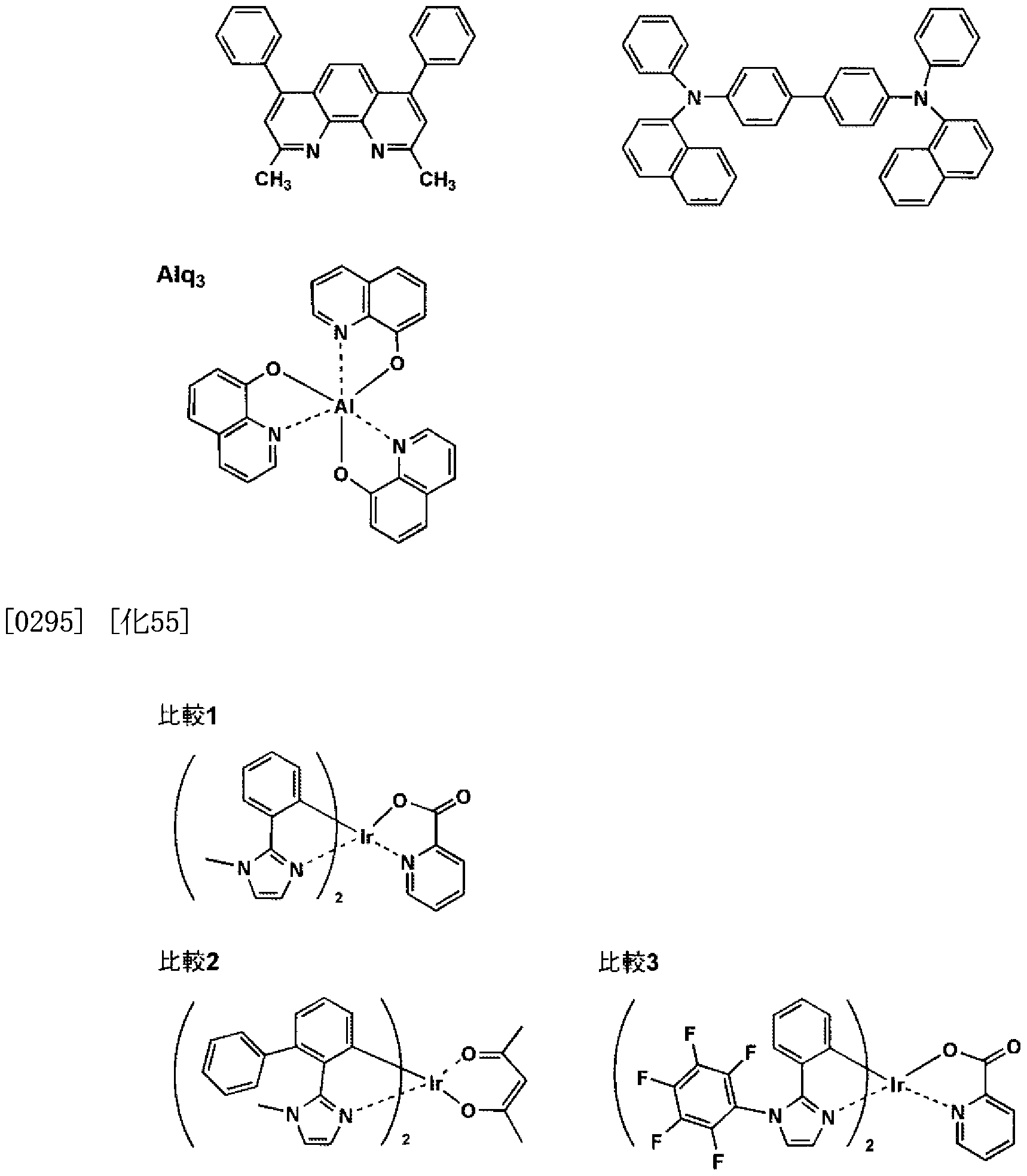
得られた有機 EL素子 1 1〜1 21を評価するに際しては、作製後の各有機 EL 素子の非発光面をガラスケースで覆い、厚み 300 mのガラス基板を封止用基板と
して用いて、周囲にシール材として、エポキシ系光硬化型接着剤 (東亞合成社製ラッ タストラック LC0629B)を適用し、これを上記陰極上に重ねて前記透明支持基板と 密着させ、ガラス基板側力も UV光を照射して、硬化させて、封止して、図 5、図 6に 示すような照明装置を形成して評価した。
[0297] 図 5は照明装置の概略図を示し、有機 EL素子 101はガラスカバー 102で覆われて いる(なお、ガラスカバーでの封止作業は、有機 EL素子 101を大気に接触させること なく窒素雰囲気下のグローブボックス(純度 99. 999%以上の高純度窒素ガスの雰 囲気下)で行った)。図 6は照明装置の断面図を示し、図 6において、 105は陰極、 1 06は有機 EL層、 107は透明電極付きガラス基板を示す。なお、ガラスカバー 102内 には窒素ガス 108が充填され、捕水剤 109が設けられている。
[0298] (外部取り出し量子効率)
有機 EL素子を室温 (約 23°C〜25°C)、 2. 5mAZcm2の定電流条件下による点灯 を行い、点灯開始直後の発光輝度 (L) [cdZm2]を測定することにより、外部取り出 し量子効率 )を算出した。
[0299] ここで、発光輝度の測定は CS - 1000 (コ-力ミノルタセンシング製)を用いた。外 部取り出し量子効率は有機 EL素子 1 1を 100とする相対値で表した。
[0300] (発光寿命)
有機 EL素子を室温下、 2. 5mAZcm2の定電流条件下による連続点灯を行い、初 期輝度の半分の輝度になるのに要する時間(て 1/2)を測定した。発光寿命は有機 E
L素子 1— 1を 100と設定する相対値で表した。
[0301] (発光色)
有機 EL素子を室温下、 2. 5mAZcm2の定電流条件下による連続点灯を行った際 の発光色を目視で評価した。
[0302] 得られた結果を表 2に示す。
[0303] [表 2]
有機 EL素子 発光 外部取り出し
発光ホスト 発光寿命 発光色 備 考 No. ド一パント 量子効率
1 - 1 H4 lr-12 100 100 肯緑 比較例
1一 2 H4 比較 1 75 95 黄緑 比較例
1 -3 H4 比較 2 109 113 黄 比較例
1 -4 H4 比較 3 112 40 淡青白 比較例
1一 5 H4 (3) 128 325 純青 本発明
1 -6 H4 (17) 133 488 純青 本発明
1 - 7 H4 (23) 129 342 純青 本発明
1 -8 H4 (34) 134 470 純青 本発明
1 -9 H4 (42) 129 445 純青 本発明
1—10 H4 (54) 135 538 本発明
1一 11 H6 (68) 141 501 本発明
1一 12 H6 (83) 139 529 純青 本発明
1 -13 H6 (95) 135 520 純青 本発明
1 -14 H6 (97) 142 649 本発明
1 -15 H6 (123) 145 588 純青 本発明
1—16 H6 (133) 141 613 本発明
1一 17 H30 (140) 152 721 本発明
1—18 H30 (154) 149 688 本発明
1一 19 H30 (176) 143 632 R 本発明
1 -20 H30 (3) 135 362 本発明
1 -21 H30 (97) 150 678 青 本発明
[0304] 表 2から、本発明に係る金属錯体を用いて作製した有機 EL素子は、比較例の有機 EL素子に比べ、高い発光効率と発光寿命の長寿命化が達成できることが明らかで ある。加えて、比較例の有機 EL素子に比べ、青色純度が高ぐ青色発光素子として 有用であることがわかる。更に、カルボリン誘導体またはカルボリン誘導体のカルボリ ン環を構成する炭化水素環の炭素原子の少なくとも一つが、更に窒素原子で置換さ れている環構造を有する誘導体を発光層に併用することにより、更に本発明の効果 の向上が見られた。
[0305] 実施例 2
《有機 EL素子 2—1の作製》
陽極としてガラス上に ITOを 150nm成膜した基板 (NHテクノグラス社製: NA— 45 )にパターユングを行った後、この ITO透明電極を設けた透明支持基板を iso—プロ ピルアルコールで超音波洗净し、乾燥窒素ガスで乾燥し、 UVオゾン洗浄を 5分間行
つた o
[0306] この透明支持基板を市販の真空蒸着装置の基板ホルダーに固定し、一方 5つのタ ンタル製抵抗加熱ボートに、 —NPD、 H2、 Ir—13、 BCP、 Alqをそれぞれ入れ、
3
真空蒸着装置 (第 1真空槽)に取り付けた。
[0307] 更に、タンタル製抵抗加熱ボートにフッ化リチウムを、タングステン製抵抗加熱ボー トにアルミニウムをそれぞれ入れ、真空蒸着装置の第 2真空槽に取り付けた。
[0308] まず、第 1の真空槽を 4 X 10—4Paまで減圧した後、 a—NPDの入った前記加熱ボ ートに通電して加熱し、蒸着速度 0. InmZ秒〜 0. 2nmZ秒で透明支持基板に膜 厚 20nmの厚さになるように蒸着し、正孔注入 Z輸送層を設けた。
[0309] 更に、 H2の入った前記加熱ボートと Ir 13の入ったボートをそれぞれ独立に通電 して発光ホストである H2と発光ドーパントである Ir— 13の蒸着速度が 100 : 6になるよ うに調節し、膜厚 30nmの厚さになるように蒸着し、発光層を設けた。
[0310] 次いで、 BCPの入った前記加熱ボートに通電して加熱し、蒸着速度 0. InmZ秒
〜0. 2nmZ秒で厚さ lOnmの正孔阻止層を設けた。更に、 Alqの入った前記加熱
3
ボートを通電して加熱し、蒸着速度 0. InmZ秒〜 0. 2nmZ秒で膜厚 20nmの電子 輸送層を設けた。
[0311] 次に、電子輸送層まで成膜した素子を真空のまま第 2真空槽に移した後、電子輸 送層の上にステンレス鋼製の長方形穴あきマスクが配置されるように装置外部力 リ モートコントロールして設置した。
[0312] 第 2真空槽を 2 X 10— 4Paまで減圧した後、フッ化リチウム入りのボートに通電して蒸 着速度 0. OlnmZ秒〜 0. 02nmZ秒で膜厚 0. 5nmの陰極バッファ一層を設け、 次 、でアルミニウムの入ったボートに通電して、蒸着速度 InmZ秒〜 2nmZ秒で膜 厚 150nmの陰極をつけ、有機 EL素子 2— 1を作製した。
[0313] 《有機 EL素子 2— 2〜2— 31の作製》
有機 EL素子 2— 1の作製において、表 3に記載のように発光ホスト、発光ドーパント 及び正孔阻止材料を変更した以外は同様にして、有機 EL素子 2— 2〜2— 31を作 製した。
[0314] [化 56]


[0315] 《有機 EL素子の評価》
得られた有機 EL素子 2— 1〜2— 31を評価するに際しては、作製後の各有機 EL 素子の非発光面をガラスケースで覆い、厚み 300 mのガラス基板を封止用基板と して用いて、周囲にシール材として、エポキシ系光硬化型接着剤 (東亞合成社製ラッ タストラック LC0629B)を適用し、これを上記陰極上に重ねて前記透明支持基板と 密着させ、ガラス基板側力も UV光を照射して、硬化させて、封止して、図 5、図 6に 示すような照明装置を形成して評価した。
[0316] 外部取り出し量子効率、発光寿命、発光色を実施例 1と同様の方法で評価を行つ た。外部取り出し量子効率、発光寿命は、有機 EL素子 2—1を 100として各々相対 値で表した。得られた結果を表 3に示す。
[0317] [表 3]
有機 EL素子 発光 発光 正孔阻止 外部取り出し
発光色 備 考
No. ホスト ド一パント 材料 量子効率 寿命
2― 1 H2 lr-13 BCP 100 100 黄緑 比較例
2 - 2 H2 比較 1 BCP 83 95 黄綠 比較例
2 - 3 H2 比較 4 BCP 110 65 比較例
2 - 4 H2 比較 5 BCP 73 70 比較例
2 - 5 H2 比較 6 BCP 90 69 比較例
2 - 6 H2 比較 7 BCP 94 100 比較例
2 - 7 H 2 比較 8 BCP 108 94 黄 比較例
2 - 8 H 2 比較 9 BCP 125 889 黄 比較例
2 - 9 H 2 (7) BCP 135 360 純青 本発明
2 -10 H2 (27) BCP 140 372 純青 本発明
2 -11 H 2 (38) BCP 142 368 純青 本発明
2 -12 H4 (56) BCP 151 582 本発明
2 -13 H4 (77) BCP 153 603 m 本発明
2 -14 H4 (97) BCP 156 707 本発明
2一 15 H4 (106) BCP 149 668 本発明
2一 16 H6 (113) BCP 154 692 本発明
2 -17 H6 (119) BCP 1 8 671 本発明
2 -18 H6 (139) BCP 159 72 ί 本発明
2 -19 H6 (146) BCP 157 764 純青 本発明
2一 20 H10 (150) BCP 155 738 純青 本発明
2 -21 H10 (154) BCP 158 756 本発明
2 -22 H10 (159) BCP 156 744 純青 本発明
2一 23 H10 (161) BCP 152 715 純青 本発明
2 -24 H 2 (7) H 5 141 399 純青 本発明
2一 25 H4 (56) H 5 156 615 本発明
2 -26 H4 (97) H5 161 738 s綠 本発明
2—27 H6 (119) H5 154 698 本発明
2 -28 H6 (,46) H5 164 822 純青 本発明
2—29 H10 (154) H26 166 798 本発明
2 -30 H10 (159) H26 163 801 純青 本発明
2 -3! H10 (161) H26 159 745 純青 本発明
[0318] 表 3から、本発明に係る金属錯体を用いて作製した有機 EL素子は、比較例の有機 EL素子に比べ、高い発光効率と発光寿命の長寿命化が達成できることが明らかで ある。加えて、比較 9を用いて長波長である有機 EL素子に比べ、本発明の有機 EL 素子材料を用いた場合、青色発光材料として申し分のな ヽ短波化効果が得られたこ とは明らかである。
[0319] 更に、カルボリン誘導体または該カルボリン誘導体のカルボリン環を構成する炭化 水素環の炭素原子の少なくとも一つが、更に窒素原子で置換されている環構造を有
する誘導体を発光層に併用することにより、更に本発明の効果の向上が見られた。
[0320] 実施例 3
《有機 EL素子 3—1の作製》
25mm X 25mm X O. 5mmのガラス支持基板上に直流電源を用い、スパッタ法に てインジウム錫酸ィ匕物(ITO、インジウム Ζ錫 = 95Ζ5モル比)の陽極を形成した (厚 み 200nm)。この陽極の表面抵抗は 10 Ω ロであった。これにポリビュルカルバゾ —ル (正孔輸送性バインダーポリマー) /Ir— 13 (青発光性オルトメタルィ匕錯体) /2 — (4—ビフエ-リル)— 5— (4— t—ブチルフエ-ル)— 1, 3, 4—ォキサジァゾ—ル( 電子輸送材) = 200/2/50質量比を溶解したジクロロエタン溶液をスピンコ—タ— で塗布し、 lOOnmの発光層を得た。この有機化合物層の上にパタ—ユングしたマス ク (発光面積が 5mm X 5mmとなるマスク)を設置し、蒸着装置内で陰極バッファ一層 としてフッ化リチウム 0. 5nm及び陰極としてアルミニウム 150nmを蒸着して陰極を設 けて、青色発光の有機 EL素子 3—1を作製した。
[0321] 《有機 EL素子 3— 2〜3— 11の作製》
有機 EL素子 3— 1の作製において、表 4に記載のように発光ドーパントを変更した 以外は同様にして、有機 EL素子 3— 2〜3— 11を作製した。
[0322] 《有機 EL素子の評価》
得られた有機 EL素子 3— 1〜3— 11を評価するに際しては、作製後の各有機 EL 素子の非発光面をガラスケースで覆い、厚み 300 mのガラス基板を封止用基板と して用いて、周囲にシール材として、エポキシ系光硬化型接着剤 (東亞合成社製ラッ タストラック LC0629B)を適用し、これを上記陰極上に重ねて前記透明支持基板と 密着させ、ガラス基板側力も UV光を照射して、硬化させて、封止して、図 5、図 6に 示すような照明装置を形成して評価した。
[0323] 次いで、下記のようにして発光輝度及び発光効率を測定した。
[0324] (発光輝度、発光効率)
東洋テク-力製ソースメジャ—ユニット 2400型を用いて、直流電圧を有機 EL素子 に印加して発光させ、 10Vの直流電圧を印加した時の発光輝度(cdZm2)と 2. 5m AZcm2の電流を通じた時の発光効率 (lmZW)を測定した。得られた結果を表 4〖こ
示す。
[0325] [表 4]

[0326] 表 4から、本発明に係る金属錯体を用いて作製した有機 EL素子は、比較例の有機
EL素子に比べ、高い発光効率と高い輝度が達成できることが明らかである。
[0327] 実施例 4
《フルカラー表示装置の作製》
(青色発光素子の作製)
実施例 1の有機 EL素子 1 18を青色発光素子として用 ヽた。
[0328] (緑色発光素子の作製)
実施例 2の有機 EL素子 2— 1にお 、て、 Ir— 13を Ir— 1に変更した以外は同様にし て、緑色発光素子を作製し、これを緑色発光素子として用いた。
(赤色発光素子の作製)
実施例 2の有機 EL素子 2— 1にお 、て、 Ir— 13を Ir— 9に変更した以外は同様にし て、赤色発光素子を作製し、これを赤色発光素子として用いた。
[0329] 上記で作製した赤色、緑色、青色発光有機 EL素子を同一基板上に並置し、図 1に 記載のような形態を有するアクティブマトリクス方式フルカラー表示装置を作製した。 図 2には、作製した前記表示装置の表示部 Aの模式図のみを示した。
[0330] 即ち、同一基板上に複数の走査線 5及びデータ線 6を含む配線部と並置した複数 の画素 3 (発光の色が赤領域の画素、緑領域の画素、青領域の画素等)とを有し、配
線部の走査線 5及び複数のデータ線 6はそれぞれ導電材料からなり、走査線 5とデ ータ線 6は格子状に直交して、直交する位置で画素 3に接続している(詳細は図示せ ず)。
[0331] 前記複数画素 3は、それぞれの発光色に対応した有機 EL素子、アクティブ素子で あるスイッチングトランジスタと駆動トランジスタそれぞれが設けられたアクティブマトリ タス方式で駆動されており、走査線 5から走査信号が印加されるとデータ線 6から画 像データ信号を受け取り、受け取った画像データに応じて発光する。このように赤、 緑、青の画素を適宜、並置することによって、フルカラー表示装置を作製した。
[0332] このフルカラー表示装置は駆動することにより、輝度が高ぐ高耐久性を有し、且つ 鮮明なフルカラー動画表示が得られることが分力つた。
[0333] 実施例 5
《白色発光素子及び白色照明装置の作製》
実施例 1の透明電極基板の電極を 20mm X 20mmにパターユングし、その上に実 施例 1と同様に正孔注入/輸送層として α— NPDを 25nmの厚さで成膜し、更に H 4の入った前記加熱ボートと例示化合物(159)の入ったボート及び Ir 9の入ったボ ートをそれぞれ独立に通電して、発光ホストである CBPと発光ドーパントである例示 化合物(159)及び Ir— 9の蒸着速度が 100 : 5 : 0. 6になるように調節し、膜厚 30nm の厚さになるように蒸着し、発光層を設けた。
[0334] 次!、で、 BCPを lOnm成膜して正孔阻止層を設けた。更に、 Alqを 40nmで成膜し
3
電子輸送層を設けた。
[0335] 次に、実施例 1と同様に電子注入層の上にステンレス鋼製の透明電極とほぼ同じ 形状の正方形穴あきマスクを設置し、陰極バッファ一層としてフッ化リチウム 0. 5nm 及び陰極としてアルミニウム 150nmを蒸着成膜した。
[0336] この素子を実施例 1と同様な方法及び同様な構造の封止缶を具備させ、図 5、図 6 に示すような平面ランプを作製した。この平面ランプに通電したところほぼ白色の光 が得られ、照明装置として使用できることが分力つた。
[0337] [化 57]
CBP

[0338] 実施例 6
《有機 EL素子 6—1の作製》
陽極として 100mm X 100mm X I. 1mmのガラス基板上に ITO (インジウムチンォ キシド)を lOOnm成膜した基板 (ΝΗテクノグラス社製 ΝΑ— 45)にパターユングを行 つた後、この ITO透明電極を設けた透明支持基板をイソプロピルアルコールで超音 波洗浄し、乾燥窒素ガスで乾燥し、 UVオゾン洗浄を 5分間行った。
[0339] この透明支持基板上に、ポリ(3, 4 エチレンジォキシチォフェン) ポリスチレンス ルホネート(PEDOTZPSSゝ Bayer社製、 Baytron P A1 4083)を純水で 70% に希釈した溶液を 3000rpm、 30秒でスピンコート法により成膜した後、 200°Cにて 1 時間乾燥し、膜厚 30nmの第 1正孔輸送層を設けた。
[0340] この基板を窒素雰囲気下に移し、第 1正孔輸送層上に、 50mgの化合物 Aを 10ml のトルエンに溶解した溶液を 1000rpm、 30秒の条件下、スピンコート法により成膜し た。 180秒間紫外光を照射し、光重合'架橋を行った後、 60°Cで 1時間真空乾燥し 第 2正孔輸送層とした。
[0341] 次に、化合物 B (60mg)、 Ir 13 (青発光性オルトメタル化錯体: 6. Omg)をトルェ ン 6mlに溶解した溶液を用い、 1000rpm、 30秒の条件下、スピンコート法により成膜 した。 15秒間紫外光を照射し、光重合'架橋を行わせ、さらに真空中 150°Cで 1時間 加熱を行い、発光層とした。
[0342] 更に、化合物 C (20mg)をトルエン 6mlに溶解した溶液を用い、 1000rpm、 30秒 の条件下、スピンコート法により成膜した。 15秒間紫外光を照射し、光重合'架橋を 行わせ、さらに真空中 80°Cで 1時間加熱を行い、正孔阻止層とした。
[0343] 続いて、この基板を真空蒸着装置の基板ホルダーに固定し、モリブデン製抵抗力口
熱ボートに Alqを 200mg入れ、真空蒸着装置に取り付けた。真空槽を 4 X 10_4Pa
3
まで減圧した後、 Alqの入った前記加熱ボートに通電して加熱し、蒸着速度 0. lnm
3
Z秒で前記電子輸送層の上に蒸着して、更に膜厚 40nmの電子輸送層を設けた。
[0344] なお、蒸着時の基板温度は室温であった。
[0345] 引き続き、フッ化リチウム 0. 5nm及びアルミニウム 11 Onmを蒸着して陰極を形成し 、青色発光の有機 EL素子 6—1を作製した。
[0346] 《有機 EL素子 6— 2〜6— 13の作製》
有機 EL素子 6— 1の作製において、表 4に記載のように発光ドーパントを変更した 以外は同様にして、有機 EL素子 6— 2〜6— 13を作製した。
[0347] 《有機 EL素子の評価》
得られた有機 EL素子を評価するに際しては、作製後の各有機 EL素子の非発光面 をガラスケースで覆い、厚み 300 mのガラス基板を封止用基板として用いて、周囲 にシール材として、エポキシ系光硬化型接着剤 (東亞合成社製ラックストラック LC06 29B)を適用し、これを上記陰極上に重ねて前記透明支持基板と密着させ、ガラス基 板側から UV光を照射して、硬化させて、封止して、図 5、図 6に示すような照明装置 を形成して評価した。
[0348] 次いで、下記のようにして発光輝度及び発光効率を測定した。
[0349] 《発光輝度、発光効率》
東洋テク-力製ソースメジャ—ユニット 2400型を用いて、直流電圧を有機 EL素子 に印加して発光させ、 10Vの直流電圧を印加した時の発光輝度(cdZm2)と 2. 5m AZcm2の電流を通じた時の発光効率 (lmZW)を測定した。評価の結果を表 5にす
[0350] [表 5]
有機 EL素子 発光 発光輝度 発光効率
No. ドーパント (cd/m2) (Im/W) 備 考
6OD CD C— 1 Ir-13 100 100 比較例
6-2 7 128 134 本発明
寸Do C c
6-3 39 137 140 本発明
57 141 141 本発明
6-5 68 135 140 本発明
95 133 132 本発明
6-7 97 143 146 本発明
116 145 148 本発明
6-9 146 151 154 本発明
6—10 154 156 156 本発明
6一 11 159 152 153 本発明
6-12 169 153 154 本発明
155 154 155 本発明
[0351] 表 5から、比較例の有機 EL素子に比べて、本発明の有機 EL素子は、高い発光効 率と高い輝度を達成できることが明らかである。
[0352] [化 58]

[0353] 実施例 7
《白色発光素子及び白色照明装置の作製》
陽極として 100mm X 100mm X I. 1mmのガラス基板上に ITO (インジウムチンォ キシド)を lOOnm成膜した基板 (ΝΗテクノグラス社製 ΝΑ— 45)にパターユングを行 つた後、この ITO透明電極を設けた透明支持基板をイソプロピルアルコールで超音 波洗浄し、乾燥窒素ガスで乾燥し、 UVオゾン洗浄を 5分間行った。
[0354] この透明支持基板上に、ポリ(3, 4 エチレンジォキシチォフェン) ポリスチレンス ルホネート(PEDOTZPSSゝ Bayer社製、 Baytron P A1 4083)を純水で 70% に希釈した溶液を 3000rpm、 30秒でスピンコート法により成膜した後、 200°Cにて 1 時間乾燥し、膜厚 30nmの第 1正孔輸送層を設けた。
[0355] この基板を窒素雰囲気下に移し、第 1正孔輸送層上に、 50mgの化合物 Aを 10ml のトルエンに溶解した溶液を 1000rpm、 30秒の条件下、スピンコート法により成膜し た。 180秒間紫外光を照射し、光重合'架橋を行った後、 60°Cで 1時間真空乾燥し 第 2正孔輸送層とした。
[0356] 次に、化合物 (60!118)、例示化合物154 (3. 0mg)、 Ir-9 (3. Omg)をトルエン 6 mlに溶解した溶液を用い、 1000rpm、 30秒の条件下、スピンコート法により成膜し た。 15秒間紫外光を照射し、光重合'架橋を行わせ、さらに真空中 150°Cで 1時間 加熱を行い、発光層とした。
[0357] 更に、化合物 C (20mg)をトルエン 6mlに溶解した溶液を用い、 1000rpm、 30秒 の条件下、スピンコート法により成膜した。 15秒間紫外光を照射し、光重合'架橋を 行わせ、さらに真空中 80°Cで 1時間加熱を行い、正孔阻止層とした。
[0358] 続いて、この基板を真空蒸着装置の基板ホルダーに固定し、モリブデン製抵抗力口 熱ボートに Alqを 200mg入れ、真空蒸着装置に取り付けた。真空槽を 4 X 10_4Pa
3
まで減圧した後、 Alqの入った前記加熱ボートに通電して加熱し、蒸着速度 0. lnm
3
Z秒で前記電子輸送層の上に蒸着して、更に膜厚 40nmの電子輸送層を設けた。
[0359] なお、蒸着時の基板温度は室温であった。
[0360] 引き続き、フッ化リチウム 0. 5nm及びアルミニウム 11 Onmを蒸着して陰極を形成し
、白色発光有機 EL素子を作製した。
[0361] この素子に通電したところほぼ白色の光が得られ、照明装置として使用出来ること
が判った。また、例示化合物 154の代わりに例示化合物 155および例示化合物 159 を用いた場合でも同様に白色の光が得られ、照明装置として使用出来ることが判つ た。
[0362] 更に、これらの白色発光有機 EL素子を用いて液晶表示装置のバックライト等、表 示装置としても使用することが可能である。
[0363] 実施例 8
《フルカラー表示装置の作製》
(青色発光素子の作製)
実施例 6と同様の方法で、緑色発光素子、赤色発光素子、青色発光素子を作成した
[0364] (青色発光素子の作製)
実施例 6の有機 EL素子 6— 10を青色発光素子として用いた。
[0365] (緑色発光素子の作製)
実施例 6の有機 EL素子 6 - 1にお 、て、 Ir— 13を Ir— 1に変更した以外は同様にし て、緑色発光素子を作製し、これを緑色発光素子として用いた。
(赤色発光素子の作製)
実施例 2の有機 EL素子 6 - 1にお 、て、 Ir— 13を Ir— 9に変更した以外は同様にし て、赤色発光素子を作製し、これを赤色発光素子として用いた。
実施例 6と同様の方法で、図 1に記載のような形態を有するアクティブマトリクス方式フ ルカラー表示装置を作製した。
[0366] このフルカラー表示装置は駆動することにより、輝度が高ぐ高耐久性を有し、且つ 鮮明なフルカラー動画表示が得られることが分力つた。さらに青色発光素子の有機 E L素子 6 - 10の代わりに有機 EL素子 6 - 11および有機 EL素子 6 - 13を用いた場 合でも、同様なフルカラー動画表示が得られることが分力つた。
Claims
[化 1] 一般式 (1>

(式中、 Zは結合する窒素原子力も数えて 3番目の原子の少なくとも 1つに、立体パラ メーター値 (Es値)が— 0. 5以下の置換基を結合している炭化水素環または複素環 を表す。 X及び Yは炭素原子または窒素原子を表し、 Aは X— Cと共に 5 6員の炭 化水素環または複素環を形成するのに必要な原子群を表す。 Bは C (R ) =C (R
01 0
)― -N = C (R )― C (R ) =N—または一 N N を表し、 R 及び R は水
2 02 01 01 02 素原子または置換基を表す。 X -L1 -Xは 2座の配位子を表し、 X Xは各々独
1 2 1 2 立に炭素原子、窒素原子または酸素原子を表す。 L1は X X
1 2と共に 2座の配位子を 形成する原子群を表す。 mlは 1 2または 3の整数を表し、 m2は 0 1または 2の整数 を表す力 ml +m2は 2または 3である。中心金属である Mは元素周期表における 8
1
10族の金属を表す。 )
前記一般式(1)で表される金属錯体が下記一般式 (2)で表されることを特徴とする請 求の範囲第 1項に記載の有機エレクト口ルミネッセンス素子。
[化 2]
-般式 (2》

(式中、 Rはイミダゾール環の窒素原子に結合する Z力 なる環のオルト位に位置す
2
る立体パラメーター値 (Es値)がー 0. 5以下の置換基を表し、 Rは水素原子または
1
置換基を表し、 nlは 1から 4の整数を表す。 Rは水素原子または置換基を表し、 n2
2
は 1から 2の整数を表す。 Zは C Cと共に 5〜6員の炭化水素環または複素環を形
1
成するのに必要な原子群を表す。 zは炭化水素環または複素環を形成するのに必
2
要な原子群を表す。 X -L1 -Xは 2座の配位子を表し、 X、 Xは各々独立に炭素
1 2 1 2
原子、窒素原子または酸素原子を表す。 L1は X、 Xと共に 2座の配位子を形成する
1 2
原子群を表す。 mlは 1、 2または 3の整数を表し、 m2は 0、 1または 2の整数を表すが 、 ml +m2は 2または 3である。中心金属である Mは元素周期表における 8〜10族
1
の金属を表す。 )
[3] 前記一般式 (2)で表される金属錯体が下記一般式 (3)で表されることを特徴とする請 求の範囲第 2項に記載の有機エレクト口ルミネッセンス素子。
[化 3] 一般式

1 子または置換基を表し、 nlは 1から 4の整数を表す。 R及び Rは水素原子または置
2 3
換基を表し、 n2は 1から 2の整数、 n3は 1から 4の整数を表す。 X—L1—Xは 2座の
1 2 配位子を表し、 X、 Xは各々独立に炭素原子、窒素原子または酸素原子を表す。 L
1 2
1は X、 Xと共に 2座の配位子を形成する原子群を表す。 mlは 1、 2または 3の整数
1 2
を表し、 m2は 0、 1または 2の整数を表す力 ml +m2は 2または 3である。中心金属 である Mは元素周期表における 8〜: LO族の金属を表す。 )
1
前記一般式 (3)で表される金属錯体が下記一般式 (4)で表されることを特徴とする請 求の範囲第 3項に記載の有機エレクト口ルミネッセンス素子。
[化 4] 一般式 (4)

(式中、 R及び は立体パラメーター値 (Es値)が— 0. 5以下の置換基を表し、 R
1 は水素原子または置換基を表し、 nlは 1から 4の整数を表す。 R及び Rは水素原子
2 3
または置換基を表し、 n2は 1から 2の整数、 n3は 1から 3の整数を表す。 X—L1—X
1 2 は 2座の配位子を表し、 X、 Xは各々独立に炭素原子、窒素原子または酸素原子を
1 2
表す。 L1は X、 Xと共に 2座の配位子を形成する原子群を表す。 mlは 1、 2または 3
1 2
の整数を表し、 m2は 0、 1または 2の整数を表す力 ml +m2は 2または 3である。中 心金属である Mは元素周期表における 8〜: L0族の金属を表す。 )
1
[5] 前記 m2が 0であることを特徴とする請求の範囲第 1項〜請求の範囲第 4項のいずれ 力 1項に記載の有機エレクト口ルミネッセンス素子。
[6] 前記立体パラメーター値 (Es値)が— 0. 5以下の置換基が電子供与性基であること
を特徴とする請求の範囲第 1項〜請求の範囲第 5項のいずれか 1項に記載の有機ェ レクト口ルミネッセンス素子。
[7] 前記中心金属 M力イリジウムであることを特徴とする請求の範囲第 1項〜請求の範
1
囲第 6項のいずれか 1項に記載の有機エレクト口ルミネッセンス素子。
[8] 前記中心金属 Mが白金であることを特徴とする請求の範囲第 1項〜請求の範囲第 6
1
項のいずれ力 1項に記載の有機エレクト口ルミネッセンス素子。
[9] 第 1発光波長が 400〜500nmの範囲内であることを特徴とする請求の範囲第 1項〜 請求の範囲第 8項のいずれか 1項に記載の有機エレクト口ルミネッセンス素子。
[10] 構成層として発光層を有することを特徴とする請求の範囲第 1項〜請求の範囲第 9 項のいずれ力 1項に記載の有機エレクト口ルミネッセンス素子。
[11] 前記発光層がカルボリン誘導体または該カルボリン誘導体のカルボリン環を構成す る炭化水素環の炭素原子の少なくとも一つが窒素原子で置換されている環構造を有 する誘導体を含有することを特徴とする請求の範囲第 10項に記載の有機エレクト口 ルミネッセンス素子。
[12] 構成層として正孔阻止層を有し、該正孔阻止層がカルボリン誘導体または該カルボ リン誘導体のカルボリン環を構成する炭化水素環の炭素原子の少なくとも一つが窒 素原子で置換されている環構造を有する誘導体を含有することを特徴とする請求の 範囲第 10項または請求の範囲第 11項に記載の有機エレクト口ルミネッセンス素子。
[13] 前記構成層の少なくともひとつが塗布法で形成されることを特徴とする請求の範囲第 10項〜請求の範囲第 12項のいずれか 1項に記載の有機エレクト口ルミネッセンス素 子。
[14] 請求の範囲第 10項〜請求の範囲第 12項のいずれか 1項に記載の有機エレクトロル ミネッセンス素子を有することを特徴とする白色発光素子。
[15] 請求の範囲第 10項〜請求の範囲第 13項のいずれか 1項に記載の有機エレクトロル ミネッセンス素子または請求の範囲第 14項に記載の白色発光素子を有することを特 徴とする表示装置。
[16] フルカラー表示であることを特徴とする請求の範囲第 15項に記載の表示装置。
[17] 請求の範囲第 10項〜請求の範囲第 13項のいずれか 1項に記載の有機エレクトロル
ミネッセンス素子または請求の範囲第 14項に記載の白色発光素子を有することを特 徴とする照明装置。
Priority Applications (2)
| Application Number | Priority Date | Filing Date | Title |
|---|---|---|---|
| JP2008501646A JP5520479B2 (ja) | 2006-02-20 | 2007-01-23 | 有機エレクトロルミネッセンス素子、白色発光素子、及び照明装置 |
| EP07707233A EP1988143A4 (en) | 2006-02-20 | 2007-01-23 | ORGANIC ELECTROLUMINESCENT ELEMENT, WHITE LIGHT EMITTING ELEMENT, DISPLAY DEVICE, AND LIGHTING DEVICE |
Applications Claiming Priority (2)
| Application Number | Priority Date | Filing Date | Title |
|---|---|---|---|
| JP2006-042061 | 2006-02-20 | ||
| JP2006042061 | 2006-02-20 |
Publications (1)
| Publication Number | Publication Date |
|---|---|
| WO2007097149A1 true WO2007097149A1 (ja) | 2007-08-30 |
Family
ID=38428599
Family Applications (2)
| Application Number | Title | Priority Date | Filing Date |
|---|---|---|---|
| PCT/JP2007/050970 WO2007097149A1 (ja) | 2006-02-20 | 2007-01-23 | 有機エレクトロルミネッセンス素子、白色発光素子、表示装置、及び照明装置 |
| PCT/JP2007/051157 WO2007097153A1 (ja) | 2006-02-20 | 2007-01-25 | 有機エレクトロルミネッセンス素子材料、有機エレクトロルミネッセンス素子、表示装置及び照明装置 |
Family Applications After (1)
| Application Number | Title | Priority Date | Filing Date |
|---|---|---|---|
| PCT/JP2007/051157 WO2007097153A1 (ja) | 2006-02-20 | 2007-01-25 | 有機エレクトロルミネッセンス素子材料、有機エレクトロルミネッセンス素子、表示装置及び照明装置 |
Country Status (4)
| Country | Link |
|---|---|
| US (2) | US20070196690A1 (ja) |
| EP (2) | EP1988143A4 (ja) |
| JP (4) | JP5520479B2 (ja) |
| WO (2) | WO2007097149A1 (ja) |
Cited By (20)
| Publication number | Priority date | Publication date | Assignee | Title |
|---|---|---|---|---|
| WO2009008367A1 (ja) * | 2007-07-12 | 2009-01-15 | Konica Minolta Holdings, Inc. | 有機エレクトロルミネッセンス素子材料、有機エレクトロルミネッセンス素子、表示装置及び照明装置 |
| JP2013004245A (ja) * | 2011-06-15 | 2013-01-07 | Konica Minolta Holdings Inc | 有機エレクトロルミネッセンス素子および照明装置 |
| KR20130036200A (ko) * | 2010-02-25 | 2013-04-11 | 유니버셜 디스플레이 코포레이션 | 인광 발광체 |
| JP2013138225A (ja) * | 2013-02-06 | 2013-07-11 | Konica Minolta Inc | 有機エレクトロルミネッセンス素子材料、有機エレクトロルミネッセンス素子、表示装置及び照明装置 |
| JP2013138226A (ja) * | 2013-02-06 | 2013-07-11 | Konica Minolta Inc | 有機エレクトロルミネッセンス素子材料、有機エレクトロルミネッセンス素子、表示装置及び照明装置 |
| JP2013147497A (ja) * | 2012-01-17 | 2013-08-01 | Universal Display Corp | 新規なヘテロレプティックイリジウム錯体 |
| EP2623508A1 (en) | 2012-02-02 | 2013-08-07 | Konica Minolta Advanced Layers, Inc. | Iridium complex compound, organic electroluminescent element material, organic electroluminescent element, illumination device and display device |
| JP2013153222A (ja) * | 2013-05-01 | 2013-08-08 | Konica Minolta Inc | 有機エレクトロルミネッセンス素子材料 |
| JP2013183036A (ja) * | 2012-03-02 | 2013-09-12 | Konica Minolta Inc | 有機エレクトロルミネッセンス素子、表示装置および照明装置 |
| JP2014043444A (ja) * | 2012-08-24 | 2014-03-13 | Universal Display Corp | フェニルイミダゾール配位子を有するリン光エミッター |
| WO2014038456A1 (ja) * | 2012-09-04 | 2014-03-13 | コニカミノルタ株式会社 | 有機エレクトロルミネッセンス素子、照明装置及び表示装置 |
| US8778506B2 (en) | 2006-02-20 | 2014-07-15 | Konica Minolta Holdings, Inc. | Organic electroluminescent element, white light emission element, full color display device and lighting device |
| JP2014152151A (ja) * | 2013-02-12 | 2014-08-25 | Konica Minolta Inc | 有機金属錯体、有機エレクトロルミネッセンス素子材料、有機エレクトロルミネッセンス素子、照明装置及び表示装置 |
| WO2014156922A1 (ja) | 2013-03-29 | 2014-10-02 | コニカミノルタ株式会社 | 異性体混合金属錯体組成物、有機エレクトロルミネッセンス素子、照明装置及び表示装置 |
| JP5609641B2 (ja) * | 2008-07-10 | 2014-10-22 | コニカミノルタ株式会社 | 有機エレクトロルミネッセンス素子、表示装置及び照明装置 |
| WO2015008851A1 (ja) * | 2013-07-17 | 2015-01-22 | 住友化学株式会社 | 組成物およびそれを用いた発光素子 |
| JP2016048796A (ja) * | 2015-11-16 | 2016-04-07 | コニカミノルタ株式会社 | 有機エレクトロルミネッセンス素子、それが具備された表示装置及び照明装置 |
| JP2017503856A (ja) * | 2014-01-13 | 2017-02-02 | メルク、パテント、ゲゼルシャフト、ミット、ベシュレンクテル、ハフツングMerck Patent GmbH | 金属錯体 |
| KR20170125737A (ko) * | 2016-05-05 | 2017-11-15 | 유니버셜 디스플레이 코포레이션 | 유기 전계발광 재료 및 디바이스 |
| JP2020007336A (ja) * | 2011-02-23 | 2020-01-16 | ユニバーサル ディスプレイ コーポレイション | 新規四座配位白金錯体 |
Families Citing this family (59)
| Publication number | Priority date | Publication date | Assignee | Title |
|---|---|---|---|---|
| JP5181448B2 (ja) * | 2006-09-13 | 2013-04-10 | コニカミノルタホールディングス株式会社 | 有機エレクトロルミネッセンス素子材料 |
| WO2008035571A1 (fr) * | 2006-09-20 | 2008-03-27 | Konica Minolta Holdings, Inc. | Élément électroluminescent organique |
| KR20170070273A (ko) | 2008-06-10 | 2017-06-21 | 유디씨 아일랜드 리미티드 | 중수소화된 전이 금속 착물 및 이의 유기 발광 다이오드에서의 용도 ⅴ |
| US20110114933A1 (en) * | 2008-06-10 | 2011-05-19 | Basf Se | Novel transition metal complexes and use thereof in organic light-emitting diodes - iv |
| KR101656793B1 (ko) * | 2008-06-10 | 2016-09-12 | 유디씨 아일랜드 리미티드 | 신규한 전이 금속 착물 및 이의 유기 발광 다이오드에서의 용도 - ⅲ |
| KR20110043581A (ko) * | 2008-06-20 | 2011-04-27 | 바스프 에스이 | 환형 포스파젠 화합물 및 유기 발광 다이오드에서 이의 용도 |
| US8815415B2 (en) * | 2008-12-12 | 2014-08-26 | Universal Display Corporation | Blue emitter with high efficiency based on imidazo[1,2-f] phenanthridine iridium complexes |
| JP5569531B2 (ja) * | 2009-10-26 | 2014-08-13 | コニカミノルタ株式会社 | 有機エレクトロルミネッセンス素子、有機エレクトロルミネッセンス素子材料、表示装置及び照明装置 |
| KR101288574B1 (ko) * | 2009-12-02 | 2013-07-22 | 제일모직주식회사 | 갭필용 충전제 및 상기 충전제를 사용한 반도체 캐패시터의 제조 방법 |
| US9005773B2 (en) | 2010-03-15 | 2015-04-14 | Semiconductor Energy Laboratory Co., Ltd. | Organometallic complex, light-emitting element, display device, electronic device, and lighting device |
| JP5507381B2 (ja) * | 2010-07-30 | 2014-05-28 | ユー・ディー・シー アイルランド リミテッド | 有機電界発光素子及び化合物 |
| JP6015451B2 (ja) * | 2011-01-12 | 2016-10-26 | コニカミノルタ株式会社 | 有機エレクトロルミネッセンス素子、照明装置及び表示装置 |
| US9238668B2 (en) | 2011-05-26 | 2016-01-19 | Arizona Board Of Regents, Acting For And On Behalf Of Arizona State University | Synthesis of platinum and palladium complexes as narrow-band phosphorescent emitters for full color displays |
| US11917901B2 (en) | 2012-08-07 | 2024-02-27 | Udc Ireland Limited | Metal complexes |
| US9882150B2 (en) | 2012-09-24 | 2018-01-30 | Arizona Board Of Regents For And On Behalf Of Arizona State University | Metal compounds, methods, and uses thereof |
| WO2014109814A2 (en) | 2012-10-26 | 2014-07-17 | Arizona Board Of Regents Acting For And On Behalf Of Arizona State University | Metal complexes, methods, and uses thereof |
| US9685617B2 (en) | 2012-11-09 | 2017-06-20 | Universal Display Corporation | Organic electronuminescent materials and devices |
| US9748500B2 (en) | 2015-01-15 | 2017-08-29 | Universal Display Corporation | Organic light emitting materials |
| US8946697B1 (en) * | 2012-11-09 | 2015-02-03 | Universal Display Corporation | Iridium complexes with aza-benzo fused ligands |
| US9634264B2 (en) | 2012-11-09 | 2017-04-25 | Universal Display Corporation | Organic electroluminescent materials and devices |
| JP5472430B2 (ja) * | 2012-11-20 | 2014-04-16 | コニカミノルタ株式会社 | 有機エレクトロルミネッセンス素子材料 |
| CN104232076B (zh) * | 2013-06-10 | 2019-01-15 | 代表亚利桑那大学的亚利桑那校董会 | 具有改进的发射光谱的磷光四齿金属络合物 |
| JP6804823B2 (ja) | 2013-10-14 | 2020-12-23 | アリゾナ・ボード・オブ・リージェンツ・オン・ビハーフ・オブ・アリゾナ・ステイト・ユニバーシティーArizona Board of Regents on behalf of Arizona State University | 白金錯体およびデバイス |
| JP6319322B2 (ja) * | 2013-12-09 | 2018-05-09 | コニカミノルタ株式会社 | 有機エレクトロルミネッセンス素子、照明装置及び表示装置 |
| US10020455B2 (en) | 2014-01-07 | 2018-07-10 | Arizona Board Of Regents On Behalf Of Arizona State University | Tetradentate platinum and palladium complex emitters containing phenyl-pyrazole and its analogues |
| KR20150127494A (ko) * | 2014-05-07 | 2015-11-17 | 삼성전자주식회사 | 유기금속 화합물 및 이를 포함한 유기 발광 소자 |
| US9941479B2 (en) | 2014-06-02 | 2018-04-10 | Arizona Board Of Regents On Behalf Of Arizona State University | Tetradentate cyclometalated platinum complexes containing 9,10-dihydroacridine and its analogues |
| US9923155B2 (en) | 2014-07-24 | 2018-03-20 | Arizona Board Of Regents On Behalf Of Arizona State University | Tetradentate platinum (II) complexes cyclometalated with functionalized phenyl carbene ligands and their analogues |
| US9920242B2 (en) | 2014-08-22 | 2018-03-20 | Arizona Board Of Regents On Behalf Of Arizona State University | Metal-assisted delayed fluorescent materials as co-host materials for fluorescent OLEDs |
| WO2016029137A1 (en) | 2014-08-22 | 2016-02-25 | Arizona Board Of Regents On Behalf Of Arizona State University | Organic light-emitting diodes with fluorescent and phosphorescent emitters |
| US10033003B2 (en) | 2014-11-10 | 2018-07-24 | Arizona Board Of Regents On Behalf Of Arizona State University | Tetradentate metal complexes with carbon group bridging ligands |
| US9865825B2 (en) | 2014-11-10 | 2018-01-09 | Arizona Board Of Regents On Behalf Of Arizona State University | Emitters based on octahedral metal complexes |
| JP6534853B2 (ja) | 2015-04-21 | 2019-06-26 | 三星ディスプレイ株式會社Samsung Display Co.,Ltd. | 有機エレクトロルミネッセンス素子用材料及びそれを用いた有機エレクトロルミネッセンス素子およびその製造方法 |
| US9879039B2 (en) | 2015-06-03 | 2018-01-30 | Arizona Board Of Regents On Behalf Of Arizona State University | Tetradentate and octahedral metal complexes containing naphthyridinocarbazole and its analogues |
| US11930662B2 (en) | 2015-06-04 | 2024-03-12 | Arizona Board Of Regents On Behalf Of Arizona State University | Transparent electroluminescent devices with controlled one-side emissive displays |
| KR102486382B1 (ko) * | 2015-08-03 | 2023-01-09 | 삼성전자주식회사 | 유기금속 화합물 및 이를 포함한 유기 발광 소자 |
| DE102015220065A1 (de) | 2015-10-15 | 2017-04-20 | Tesa Se | Klebemasse, insbesondere für stripbare Klebestreifen, und Verwendung zur Verklebung auf gestrichener Raufasertapete |
| KR20220000988A (ko) | 2016-01-29 | 2022-01-04 | 스미또모 가가꾸 가부시키가이샤 | 조성물, 인광 발광성 화합물 및 발광 소자 |
| KR20170108845A (ko) * | 2016-03-18 | 2017-09-27 | 가부시키가이샤 한도오따이 에네루기 켄큐쇼 | 유기 금속 착체, 발광 소자, 발광 장치, 전자 기기 및 조명 장치 |
| US11335865B2 (en) | 2016-04-15 | 2022-05-17 | Arizona Board Of Regents On Behalf Of Arizona State University | OLED with multi-emissive material layer |
| GB2550203A (en) * | 2016-05-13 | 2017-11-15 | Sumitomo Chemical Co | Light-emitting compound |
| US10177323B2 (en) | 2016-08-22 | 2019-01-08 | Arizona Board Of Regents On Behalf Of Arizona State University | Tetradentate platinum (II) and palladium (II) complexes and octahedral iridium complexes employing azepine functional groups and their analogues |
| US10822363B2 (en) | 2016-10-12 | 2020-11-03 | Arizona Board Of Regents On Behalf Of Arizona State University | Narrow band red phosphorescent tetradentate platinum (II) complexes |
| US11545636B2 (en) * | 2016-12-15 | 2023-01-03 | Universal Display Corporation | Organic electroluminescent materials and devices |
| US11183670B2 (en) | 2016-12-16 | 2021-11-23 | Arizona Board Of Regents On Behalf Of Arizona State University | Organic light emitting diode with split emissive layer |
| KR20190139835A (ko) | 2017-01-27 | 2019-12-18 | 아리조나 보드 오브 리젠츠 온 비하프 오브 아리조나 스테이트 유니버시티 | 피리도-피롤로-아크리딘 및 유사체를 사용하는 금속 보조 지연 형광 이미터 |
| CN110547049A (zh) | 2017-04-27 | 2019-12-06 | 住友化学株式会社 | 组合物和使用了该组合物的发光元件 |
| CN110574497B (zh) | 2017-04-27 | 2022-10-18 | 住友化学株式会社 | 组合物和使用了该组合物的发光元件 |
| KR102527229B1 (ko) * | 2017-05-10 | 2023-05-02 | 삼성디스플레이 주식회사 | 유기금속 화합물 및 이를 포함한 유기 발광 소자 |
| US11101435B2 (en) | 2017-05-19 | 2021-08-24 | Arizona Board Of Regents On Behalf Of Arizona State University | Tetradentate platinum and palladium complexes based on biscarbazole and analogues |
| US10516117B2 (en) | 2017-05-19 | 2019-12-24 | Arizona Board Of Regents On Behalf Of Arizona State University | Metal-assisted delayed fluorescent emttters employing benzo-imidazo-phenanthridine and analogues |
| KR20200065064A (ko) | 2017-10-17 | 2020-06-08 | 지안 리 | 표시 및 조명 분야용 단색성 이미터로서의, 바람직한 분자 배향을 갖는 인광성 엑시머 |
| US11647643B2 (en) | 2017-10-17 | 2023-05-09 | Arizona Board Of Regents On Behalf Of Arizona State University | Hole-blocking materials for organic light emitting diodes |
| US11878988B2 (en) | 2019-01-24 | 2024-01-23 | Arizona Board Of Regents On Behalf Of Arizona State University | Blue phosphorescent emitters employing functionalized imidazophenthridine and analogues |
| US11594691B2 (en) | 2019-01-25 | 2023-02-28 | Arizona Board Of Regents On Behalf Of Arizona State University | Light outcoupling efficiency of phosphorescent OLEDs by mixing horizontally aligned fluorescent emitters |
| JP7263871B2 (ja) | 2019-03-25 | 2023-04-25 | セイコーエプソン株式会社 | テンプ、ムーブメントおよび機械式時計 |
| US11785838B2 (en) | 2019-10-02 | 2023-10-10 | Arizona Board Of Regents On Behalf Of Arizona State University | Green and red organic light-emitting diodes employing excimer emitters |
| JP7216754B2 (ja) | 2020-03-31 | 2023-02-01 | 住友化学株式会社 | 組成物及びそれを含有する発光素子 |
| US11945985B2 (en) | 2020-05-19 | 2024-04-02 | Arizona Board Of Regents On Behalf Of Arizona State University | Metal assisted delayed fluorescent emitters for organic light-emitting diodes |
Citations (102)
| Publication number | Priority date | Publication date | Assignee | Title |
|---|---|---|---|---|
| JPS63264692A (ja) | 1987-03-02 | 1988-11-01 | イーストマン・コダック・カンパニー | 改良薄膜発光帯をもつ電場発光デバイス |
| US5061569A (en) | 1990-07-26 | 1991-10-29 | Eastman Kodak Company | Electroluminescent device with organic electroluminescent medium |
| JPH03255190A (ja) | 1990-01-22 | 1991-11-14 | Pioneer Electron Corp | 電界発光素子 |
| JPH04308688A (ja) | 1991-04-08 | 1992-10-30 | Pioneer Electron Corp | 有機エレクトロルミネッセンス素子 |
| JPH06325871A (ja) | 1993-05-18 | 1994-11-25 | Mitsubishi Kasei Corp | 有機電界発光素子 |
| JPH08288069A (ja) | 1995-04-07 | 1996-11-01 | Sanyo Electric Co Ltd | 有機エレクトロルミネッセンス素子 |
| JPH0917574A (ja) | 1995-04-27 | 1997-01-17 | Pioneer Electron Corp | 有機エレクトロルミネッセンス素子 |
| JPH0945479A (ja) | 1995-07-27 | 1997-02-14 | Hewlett Packard Co <Hp> | 有機エレクトロルミネセンス装置及び有機エレクトロルミネセンス装置の製造方法 |
| JPH09260062A (ja) | 1996-03-25 | 1997-10-03 | Tdk Corp | 有機エレクトロルミネセンス素子 |
| JPH1074586A (ja) | 1996-07-29 | 1998-03-17 | Eastman Kodak Co | エレクトロルミネセンスデバイスで用いられる二層電子注入電極 |
| JPH11204258A (ja) | 1998-01-09 | 1999-07-30 | Sony Corp | 電界発光素子及びその製造方法 |
| JPH11204359A (ja) | 1998-01-14 | 1999-07-30 | Tokin Corp | 圧粉磁芯の製造方法と製造装置 |
| US6097147A (en) | 1998-09-14 | 2000-08-01 | The Trustees Of Princeton University | Structure for high efficiency electroluminescent device |
| JP3093796B2 (ja) | 1992-08-28 | 2000-10-03 | 出光興産株式会社 | 電荷注入補助材及びそれを含有する有機エレクトロルミネッセンス素子 |
| WO2000070655A2 (en) | 1999-05-13 | 2000-11-23 | The Trustees Of Princeton University | Very high efficiency organic light emitting devices based on electrophosphorescence |
| JP2001181617A (ja) | 1999-12-27 | 2001-07-03 | Fuji Photo Film Co Ltd | オルトメタル化白金錯体からなる発光素子材料および発光素子 |
| JP2001181616A (ja) | 1999-12-27 | 2001-07-03 | Fuji Photo Film Co Ltd | オルトメタル化パラジウム錯体からなる発光素子材料および発光素子 |
| JP2001247859A (ja) | 1999-12-27 | 2001-09-14 | Fuji Photo Film Co Ltd | オルトメタル化イリジウム錯体からなる発光素子材料、発光素子および新規イリジウム錯体 |
| JP2001257076A (ja) | 2000-03-13 | 2001-09-21 | Tdk Corp | 有機el素子 |
| JP2001313178A (ja) | 2000-04-28 | 2001-11-09 | Pioneer Electronic Corp | 有機エレクトロルミネッセンス素子 |
| JP2001313179A (ja) | 2000-05-01 | 2001-11-09 | Mitsubishi Chemicals Corp | 有機電界発光素子 |
| JP2001319779A (ja) | 2000-05-02 | 2001-11-16 | Fuji Photo Film Co Ltd | 発光素子 |
| JP2001319780A (ja) | 2000-05-02 | 2001-11-16 | Fuji Photo Film Co Ltd | 発光素子 |
| WO2001093642A1 (en) | 2000-05-30 | 2001-12-06 | The Trustees Of Princeton University | Phosphorescent organic light emitting devices |
| JP2001345183A (ja) | 2000-03-28 | 2001-12-14 | Fuji Photo Film Co Ltd | 高効率赤色発光素子、イリジウム錯体から成る発光素子材料及び新規イリジウム錯体 |
| JP2001357977A (ja) | 2000-06-12 | 2001-12-26 | Fuji Photo Film Co Ltd | 有機電界発光素子 |
| JP2002008860A (ja) | 2000-04-18 | 2002-01-11 | Mitsubishi Chemicals Corp | 有機電界発光素子 |
| JP2002015871A (ja) | 2000-04-27 | 2002-01-18 | Toray Ind Inc | 発光素子 |
| JP2002043056A (ja) | 2000-07-19 | 2002-02-08 | Canon Inc | 発光素子 |
| JP2002050483A (ja) | 2000-05-22 | 2002-02-15 | Showa Denko Kk | 有機エレクトロルミネッセンス素子および発光材料 |
| JP2002050484A (ja) | 2000-05-22 | 2002-02-15 | Semiconductor Energy Lab Co Ltd | 発光装置および電気器具 |
| WO2002015645A1 (en) | 2000-08-11 | 2002-02-21 | The Trustees Of Princeton University | Organometallic compounds and emission-shifting organic electrophosphorescence |
| JP2002062824A (ja) | 2000-06-05 | 2002-02-28 | Semiconductor Energy Lab Co Ltd | 発光装置 |
| JP2002075645A (ja) | 2000-08-29 | 2002-03-15 | Semiconductor Energy Lab Co Ltd | 発光装置 |
| JP2002083684A (ja) | 2000-06-23 | 2002-03-22 | Semiconductor Energy Lab Co Ltd | 発光装置 |
| JP2002100474A (ja) | 2000-09-25 | 2002-04-05 | Kyocera Corp | 有機エレクトロルミネッセンス素子 |
| JP2002100476A (ja) | 2000-07-17 | 2002-04-05 | Fuji Photo Film Co Ltd | 発光素子及びアゾール化合物 |
| JP2002105445A (ja) | 2000-09-29 | 2002-04-10 | Fuji Photo Film Co Ltd | 有機発光素子材料及びそれを用いた有機発光素子 |
| JP2002117978A (ja) | 2000-07-17 | 2002-04-19 | Fuji Photo Film Co Ltd | 発光素子及びイリジウム錯体 |
| JP2002141173A (ja) | 2000-08-22 | 2002-05-17 | Semiconductor Energy Lab Co Ltd | 発光装置 |
| JP2002170684A (ja) | 2000-09-21 | 2002-06-14 | Fuji Photo Film Co Ltd | 発光素子及びイリジウム錯体 |
| JP2002173674A (ja) | 2000-09-21 | 2002-06-21 | Fuji Photo Film Co Ltd | 発光素子および新規レニウム錯体 |
| JP2002175884A (ja) | 2000-09-26 | 2002-06-21 | Canon Inc | 発光素子及び発光素子用金属配位化合物 |
| JP2002184582A (ja) | 2000-09-28 | 2002-06-28 | Semiconductor Energy Lab Co Ltd | 発光装置 |
| JP2002203679A (ja) | 2000-12-27 | 2002-07-19 | Fuji Photo Film Co Ltd | 発光素子 |
| JP2002203683A (ja) | 2000-10-30 | 2002-07-19 | Toyota Central Res & Dev Lab Inc | 有機電界発光素子 |
| JP2002203678A (ja) | 2000-12-27 | 2002-07-19 | Fuji Photo Film Co Ltd | 発光素子 |
| JP2002525833A (ja) | 1998-09-25 | 2002-08-13 | アイシス イノヴェイション リミテッド | 二価ランタノイド金属錯体 |
| JP2002226495A (ja) | 2000-11-29 | 2002-08-14 | Canon Inc | 金属配位化合物、発光素子及び表示装置 |
| JP2002231453A (ja) | 2000-11-30 | 2002-08-16 | Mitsubishi Chemicals Corp | 有機電界発光素子 |
| JP2002234888A (ja) | 2001-02-09 | 2002-08-23 | Mitsui Chemicals Inc | アミン化合物および該化合物を含有する有機電界発光素子 |
| JP2002235076A (ja) | 2001-02-09 | 2002-08-23 | Fuji Photo Film Co Ltd | 遷移金属錯体及びそれからなる発光素子用材料、並びに発光素子 |
| JP2002234894A (ja) | 2000-11-29 | 2002-08-23 | Canon Inc | 金属配位化合物、発光素子及び表示装置 |
| JP2002241751A (ja) | 2001-02-21 | 2002-08-28 | Fuji Photo Film Co Ltd | 発光素子用材料及び発光素子 |
| JP2002255934A (ja) | 2000-12-25 | 2002-09-11 | Fuji Photo Film Co Ltd | 新規化合物、その重合体、それらを利用した発光素子材料およびその発光素子 |
| JP2002260861A (ja) | 2001-01-02 | 2002-09-13 | Eastman Kodak Co | 有機発光デバイス |
| JP2002280180A (ja) | 2001-03-16 | 2002-09-27 | Canon Inc | 有機発光素子 |
| JP2002280178A (ja) | 2001-03-16 | 2002-09-27 | Canon Inc | 有機発光素子 |
| JP2002280179A (ja) | 2001-03-16 | 2002-09-27 | Canon Inc | 有機発光素子 |
| JP2002280183A (ja) | 2000-12-28 | 2002-09-27 | Toshiba Corp | 有機el素子および表示装置 |
| JP2002299060A (ja) | 2001-03-30 | 2002-10-11 | Fuji Photo Film Co Ltd | 有機発光素子 |
| JP2002305083A (ja) | 2001-04-04 | 2002-10-18 | Mitsubishi Chemicals Corp | 有機電界発光素子 |
| JP2002302671A (ja) | 2000-02-10 | 2002-10-18 | Fuji Photo Film Co Ltd | イリジウム錯体からなる発光素子材料及び発光素子 |
| JP2002302516A (ja) | 2001-04-03 | 2002-10-18 | Fuji Photo Film Co Ltd | 新規ポリマーおよびそれを用いた発光素子 |
| JP2002305084A (ja) | 2000-12-25 | 2002-10-18 | Fuji Photo Film Co Ltd | 新規インドール誘導体およびそれを利用した発光素子 |
| JP2002308855A (ja) | 2001-04-05 | 2002-10-23 | Fuji Photo Film Co Ltd | 新規化合物、およびそれを用いた発光素子 |
| JP2002308837A (ja) | 2001-04-05 | 2002-10-23 | Fuji Photo Film Co Ltd | 新規化合物、およびそれを用いた発光素子 |
| JP2002319491A (ja) | 2000-08-24 | 2002-10-31 | Fuji Photo Film Co Ltd | 発光素子及び新規重合体子 |
| JP2002324679A (ja) | 2001-04-26 | 2002-11-08 | Honda Motor Co Ltd | 有機エレクトロルミネッセンス素子 |
| JP2002334788A (ja) | 2001-03-09 | 2002-11-22 | Sony Corp | 有機電界発光素子 |
| JP2002334786A (ja) | 2001-03-09 | 2002-11-22 | Sony Corp | 有機電界発光素子 |
| JP2002334789A (ja) | 2001-03-09 | 2002-11-22 | Sony Corp | 有機電界発光素子 |
| JP2002332292A (ja) | 2001-03-08 | 2002-11-22 | Canon Inc | 金属配位化合物、電界発光素子及び表示装置 |
| JP2002334787A (ja) | 2001-03-09 | 2002-11-22 | Sony Corp | 有機電界発光素子 |
| JP2002332291A (ja) | 2001-03-08 | 2002-11-22 | Canon Inc | 金属配位化合物、電界発光素子及び表示装置 |
| JP2002540572A (ja) | 1999-03-23 | 2002-11-26 | ザ ユニバーシティー オブ サザン カリフォルニア | 有機ledの燐光性ドーパントとしてのシクロメタル化金属錯体 |
| JP2002338579A (ja) | 2001-03-16 | 2002-11-27 | Fuji Photo Film Co Ltd | ヘテロ環化合物及びそれを用いた発光素子 |
| JP2002338588A (ja) | 2001-03-14 | 2002-11-27 | Canon Inc | 金属配位化合物、電界発光素子及び表示装置 |
| JP2002343572A (ja) | 2001-03-14 | 2002-11-29 | Canon Inc | ポルフィリン誘導体化合物を用いた発光素子および表示装置 |
| JP2002343568A (ja) | 2001-05-10 | 2002-11-29 | Sony Corp | 有機電界発光素子 |
| JP2002352957A (ja) | 2001-05-23 | 2002-12-06 | Honda Motor Co Ltd | 有機エレクトロルミネッセンス素子 |
| JP2002352960A (ja) | 2001-05-29 | 2002-12-06 | Hitachi Ltd | 薄膜電界発光素子 |
| JP2002359082A (ja) | 2001-03-28 | 2002-12-13 | Semiconductor Energy Lab Co Ltd | 有機発光素子および前記素子を用いた発光装置 |
| JP2002363227A (ja) | 2001-04-03 | 2002-12-18 | Fuji Photo Film Co Ltd | 新規ポリマーおよびそれを用いた発光素子 |
| JP2002363552A (ja) | 2001-03-08 | 2002-12-18 | Univ Of Hong Kong | 有機金属発光材料 |
| JP2003003165A (ja) | 2001-06-25 | 2003-01-08 | Showa Denko Kk | 有機発光素子および発光材料 |
| JP2003007469A (ja) | 2001-06-25 | 2003-01-10 | Canon Inc | 発光素子及び表示装置 |
| JP2003007471A (ja) | 2001-04-13 | 2003-01-10 | Semiconductor Energy Lab Co Ltd | 有機発光素子および前記素子を用いた発光装置 |
| JP2003027048A (ja) | 2001-07-11 | 2003-01-29 | Fuji Photo Film Co Ltd | 発光素子 |
| JP2003031366A (ja) | 2001-07-11 | 2003-01-31 | Semiconductor Energy Lab Co Ltd | ドーパントを用いた有機発光素子および発光装置 |
| JP2003109758A (ja) | 2001-09-27 | 2003-04-11 | Konica Corp | 有機エレクトロルミネッセンス素子 |
| WO2004085450A2 (en) | 2003-03-24 | 2004-10-07 | The University Of Southern California | Phenyl-pyrazole complexes of ir |
| JP2004327313A (ja) * | 2003-04-25 | 2004-11-18 | Fuji Photo Film Co Ltd | 有機電界発光素子 |
| WO2005007767A2 (ja) | 2003-07-22 | 2005-01-27 | Idemitsu Kosan Co | 金属錯体化合物及びそれを用いた有機エレクトロルミネッセンス素子 |
| JP2005053912A (ja) | 2003-08-07 | 2005-03-03 | Samsung Sdi Co Ltd | イリジウム化合物及びそれを採用した有機電界発光素子 |
| JP2005068110A (ja) | 2003-08-27 | 2005-03-17 | Mitsubishi Chemicals Corp | 有機金属錯体、発光材料、および有機電界発光素子 |
| US6936716B1 (en) * | 2004-05-17 | 2005-08-30 | Au Optronics Corp. | Organometallic complex for organic electroluminescent device |
| JP2005255890A (ja) * | 2004-03-12 | 2005-09-22 | Toyo Ink Mfg Co Ltd | 有機エレクトロルミネッセンス素子用材料およびそれを用いた有機エレクトロルミネッセンス素子 |
| WO2005123873A1 (ja) * | 2004-06-17 | 2005-12-29 | Konica Minolta Holdings, Inc. | 有機エレクトロルミネッセンス素子材料、有機エレクトロルミネッセンス素子、表示装置及び照明装置 |
| US20060008670A1 (en) | 2004-07-06 | 2006-01-12 | Chun Lin | Organic light emitting materials and devices |
| WO2006009024A1 (ja) | 2004-07-23 | 2006-01-26 | Konica Minolta Holdings, Inc. | 有機エレクトロルミネッセンス素子、表示装置及び照明装置 |
| WO2006121811A1 (en) * | 2005-05-06 | 2006-11-16 | Universal Display Corporation | Stability oled materials and devices with improved stability |
Family Cites Families (21)
| Publication number | Priority date | Publication date | Assignee | Title |
|---|---|---|---|---|
| US5294870A (en) * | 1991-12-30 | 1994-03-15 | Eastman Kodak Company | Organic electroluminescent multicolor image display device |
| US5707745A (en) * | 1994-12-13 | 1998-01-13 | The Trustees Of Princeton University | Multicolor organic light emitting devices |
| US6461747B1 (en) * | 1999-07-22 | 2002-10-08 | Fuji Photo Co., Ltd. | Heterocyclic compounds, materials for light emitting devices and light emitting devices using the same |
| US9697650B2 (en) | 2000-06-09 | 2017-07-04 | Flash Seats, Llc | Method and system for access verification within a venue |
| US6687266B1 (en) * | 2002-11-08 | 2004-02-03 | Universal Display Corporation | Organic light emitting materials and devices |
| WO2004053019A1 (ja) * | 2002-12-12 | 2004-06-24 | Idemitsu Kosan Co., Ltd. | 有機エレクトロルミネッセンス素子用材料及びそれを用いた有機エレクトロルミネッセンス素子 |
| US7326475B2 (en) * | 2003-04-23 | 2008-02-05 | Konica Minolta Holdings, Inc. | Material for organic electroluminescent device, organic electroluminescent device, illuminating device and display |
| JP4203732B2 (ja) * | 2003-06-12 | 2009-01-07 | ソニー株式会社 | 有機電界発光材料、有機電界発光素子および含複素環イリジウム錯体化合物 |
| US7795801B2 (en) * | 2003-09-30 | 2010-09-14 | Konica Minolta Holdings, Inc. | Organic electroluminescent element, illuminator, display and compound |
| WO2005117865A1 (en) * | 2004-06-02 | 2005-12-15 | F. Hoffmann-La Roche Ag | Naphthaline derivatives useful as histamine-3-receptor ligands |
| WO2005117885A1 (en) * | 2004-06-04 | 2005-12-15 | Bioniche Life Sciences Inc. | Use of imatinib to treat liver disorders and viral infections |
| TWI260339B (en) * | 2004-10-07 | 2006-08-21 | Au Optronics Corp | Organometallic compound and organic electroluminescent device including the same |
| US20110152326A1 (en) | 2005-03-28 | 2011-06-23 | Takeshi Hanazawa | Substituted aryloxoethyl cyclopropanecarboxamide compounds as vr1 receptor antagonists |
| JP2006282319A (ja) | 2005-03-31 | 2006-10-19 | Jfe Steel Kk | コンベアベルトの縦裂き検知方法および装置 |
| US8231983B2 (en) * | 2005-04-18 | 2012-07-31 | Konica Minolta Holdings Inc. | Organic electroluminescent device, display and illuminating device |
| US7902374B2 (en) * | 2005-05-06 | 2011-03-08 | Universal Display Corporation | Stability OLED materials and devices |
| US8148891B2 (en) * | 2005-10-04 | 2012-04-03 | Universal Display Corporation | Electron impeding layer for high efficiency phosphorescent OLEDs |
| JP5072312B2 (ja) * | 2005-10-18 | 2012-11-14 | 株式会社半導体エネルギー研究所 | 有機金属錯体及びそれを用いた発光素子、発光装置 |
| WO2007069569A1 (ja) * | 2005-12-15 | 2007-06-21 | Idemitsu Kosan Co., Ltd. | 有機エレクトロルミネッセンス素子用材料及びそれを用いた有機エレクトロルミネッセンス素子 |
| US7651791B2 (en) * | 2005-12-15 | 2010-01-26 | Idemitsu Kosan Co., Ltd. | Material for organic electroluminescence device and electroluminescence device employing the same |
| JP5520479B2 (ja) | 2006-02-20 | 2014-06-11 | コニカミノルタ株式会社 | 有機エレクトロルミネッセンス素子、白色発光素子、及び照明装置 |
-
2007
- 2007-01-23 JP JP2008501646A patent/JP5520479B2/ja not_active Expired - Fee Related
- 2007-01-23 EP EP07707233A patent/EP1988143A4/en not_active Ceased
- 2007-01-23 WO PCT/JP2007/050970 patent/WO2007097149A1/ja active Application Filing
- 2007-01-25 WO PCT/JP2007/051157 patent/WO2007097153A1/ja active Application Filing
- 2007-01-25 EP EP07707404A patent/EP1988144A4/en not_active Withdrawn
- 2007-01-25 JP JP2008501649A patent/JP5104751B2/ja not_active Expired - Fee Related
- 2007-02-15 US US11/707,232 patent/US20070196690A1/en not_active Abandoned
- 2007-02-16 US US11/708,110 patent/US8778506B2/en not_active Expired - Fee Related
-
2012
- 2012-07-30 JP JP2012168770A patent/JP5516668B2/ja active Active
- 2012-07-30 JP JP2012168225A patent/JP5708588B2/ja active Active
Patent Citations (103)
| Publication number | Priority date | Publication date | Assignee | Title |
|---|---|---|---|---|
| JPS63264692A (ja) | 1987-03-02 | 1988-11-01 | イーストマン・コダック・カンパニー | 改良薄膜発光帯をもつ電場発光デバイス |
| JPH03255190A (ja) | 1990-01-22 | 1991-11-14 | Pioneer Electron Corp | 電界発光素子 |
| US5061569A (en) | 1990-07-26 | 1991-10-29 | Eastman Kodak Company | Electroluminescent device with organic electroluminescent medium |
| JPH04308688A (ja) | 1991-04-08 | 1992-10-30 | Pioneer Electron Corp | 有機エレクトロルミネッセンス素子 |
| JP3093796B2 (ja) | 1992-08-28 | 2000-10-03 | 出光興産株式会社 | 電荷注入補助材及びそれを含有する有機エレクトロルミネッセンス素子 |
| JPH06325871A (ja) | 1993-05-18 | 1994-11-25 | Mitsubishi Kasei Corp | 有機電界発光素子 |
| JPH08288069A (ja) | 1995-04-07 | 1996-11-01 | Sanyo Electric Co Ltd | 有機エレクトロルミネッセンス素子 |
| JPH0917574A (ja) | 1995-04-27 | 1997-01-17 | Pioneer Electron Corp | 有機エレクトロルミネッセンス素子 |
| JPH0945479A (ja) | 1995-07-27 | 1997-02-14 | Hewlett Packard Co <Hp> | 有機エレクトロルミネセンス装置及び有機エレクトロルミネセンス装置の製造方法 |
| JPH09260062A (ja) | 1996-03-25 | 1997-10-03 | Tdk Corp | 有機エレクトロルミネセンス素子 |
| JPH1074586A (ja) | 1996-07-29 | 1998-03-17 | Eastman Kodak Co | エレクトロルミネセンスデバイスで用いられる二層電子注入電極 |
| JPH11204258A (ja) | 1998-01-09 | 1999-07-30 | Sony Corp | 電界発光素子及びその製造方法 |
| JPH11204359A (ja) | 1998-01-14 | 1999-07-30 | Tokin Corp | 圧粉磁芯の製造方法と製造装置 |
| US6097147A (en) | 1998-09-14 | 2000-08-01 | The Trustees Of Princeton University | Structure for high efficiency electroluminescent device |
| JP2002525808A (ja) | 1998-09-14 | 2002-08-13 | ザ、トラスティーズ オブ プリンストン ユニバーシティ | 高効率の電界発光デバイスのための構造 |
| JP2002525833A (ja) | 1998-09-25 | 2002-08-13 | アイシス イノヴェイション リミテッド | 二価ランタノイド金属錯体 |
| JP2002540572A (ja) | 1999-03-23 | 2002-11-26 | ザ ユニバーシティー オブ サザン カリフォルニア | 有機ledの燐光性ドーパントとしてのシクロメタル化金属錯体 |
| WO2000070655A2 (en) | 1999-05-13 | 2000-11-23 | The Trustees Of Princeton University | Very high efficiency organic light emitting devices based on electrophosphorescence |
| JP2001181617A (ja) | 1999-12-27 | 2001-07-03 | Fuji Photo Film Co Ltd | オルトメタル化白金錯体からなる発光素子材料および発光素子 |
| JP2001181616A (ja) | 1999-12-27 | 2001-07-03 | Fuji Photo Film Co Ltd | オルトメタル化パラジウム錯体からなる発光素子材料および発光素子 |
| JP2001247859A (ja) | 1999-12-27 | 2001-09-14 | Fuji Photo Film Co Ltd | オルトメタル化イリジウム錯体からなる発光素子材料、発光素子および新規イリジウム錯体 |
| JP2002302671A (ja) | 2000-02-10 | 2002-10-18 | Fuji Photo Film Co Ltd | イリジウム錯体からなる発光素子材料及び発光素子 |
| JP2001257076A (ja) | 2000-03-13 | 2001-09-21 | Tdk Corp | 有機el素子 |
| JP2001345183A (ja) | 2000-03-28 | 2001-12-14 | Fuji Photo Film Co Ltd | 高効率赤色発光素子、イリジウム錯体から成る発光素子材料及び新規イリジウム錯体 |
| JP2002008860A (ja) | 2000-04-18 | 2002-01-11 | Mitsubishi Chemicals Corp | 有機電界発光素子 |
| JP2002015871A (ja) | 2000-04-27 | 2002-01-18 | Toray Ind Inc | 発光素子 |
| JP2001313178A (ja) | 2000-04-28 | 2001-11-09 | Pioneer Electronic Corp | 有機エレクトロルミネッセンス素子 |
| JP2001313179A (ja) | 2000-05-01 | 2001-11-09 | Mitsubishi Chemicals Corp | 有機電界発光素子 |
| JP2001319779A (ja) | 2000-05-02 | 2001-11-16 | Fuji Photo Film Co Ltd | 発光素子 |
| JP2001319780A (ja) | 2000-05-02 | 2001-11-16 | Fuji Photo Film Co Ltd | 発光素子 |
| JP2002050483A (ja) | 2000-05-22 | 2002-02-15 | Showa Denko Kk | 有機エレクトロルミネッセンス素子および発光材料 |
| JP2002050484A (ja) | 2000-05-22 | 2002-02-15 | Semiconductor Energy Lab Co Ltd | 発光装置および電気器具 |
| WO2001093642A1 (en) | 2000-05-30 | 2001-12-06 | The Trustees Of Princeton University | Phosphorescent organic light emitting devices |
| JP2002062824A (ja) | 2000-06-05 | 2002-02-28 | Semiconductor Energy Lab Co Ltd | 発光装置 |
| JP2001357977A (ja) | 2000-06-12 | 2001-12-26 | Fuji Photo Film Co Ltd | 有機電界発光素子 |
| JP2002083684A (ja) | 2000-06-23 | 2002-03-22 | Semiconductor Energy Lab Co Ltd | 発光装置 |
| JP2002100476A (ja) | 2000-07-17 | 2002-04-05 | Fuji Photo Film Co Ltd | 発光素子及びアゾール化合物 |
| JP2002117978A (ja) | 2000-07-17 | 2002-04-19 | Fuji Photo Film Co Ltd | 発光素子及びイリジウム錯体 |
| JP2002043056A (ja) | 2000-07-19 | 2002-02-08 | Canon Inc | 発光素子 |
| WO2002015645A1 (en) | 2000-08-11 | 2002-02-21 | The Trustees Of Princeton University | Organometallic compounds and emission-shifting organic electrophosphorescence |
| JP2002141173A (ja) | 2000-08-22 | 2002-05-17 | Semiconductor Energy Lab Co Ltd | 発光装置 |
| JP2002319491A (ja) | 2000-08-24 | 2002-10-31 | Fuji Photo Film Co Ltd | 発光素子及び新規重合体子 |
| JP2002075645A (ja) | 2000-08-29 | 2002-03-15 | Semiconductor Energy Lab Co Ltd | 発光装置 |
| JP2002173674A (ja) | 2000-09-21 | 2002-06-21 | Fuji Photo Film Co Ltd | 発光素子および新規レニウム錯体 |
| JP2002170684A (ja) | 2000-09-21 | 2002-06-14 | Fuji Photo Film Co Ltd | 発光素子及びイリジウム錯体 |
| JP2002100474A (ja) | 2000-09-25 | 2002-04-05 | Kyocera Corp | 有機エレクトロルミネッセンス素子 |
| JP2002175884A (ja) | 2000-09-26 | 2002-06-21 | Canon Inc | 発光素子及び発光素子用金属配位化合物 |
| JP2002184582A (ja) | 2000-09-28 | 2002-06-28 | Semiconductor Energy Lab Co Ltd | 発光装置 |
| JP2002105445A (ja) | 2000-09-29 | 2002-04-10 | Fuji Photo Film Co Ltd | 有機発光素子材料及びそれを用いた有機発光素子 |
| JP2002203683A (ja) | 2000-10-30 | 2002-07-19 | Toyota Central Res & Dev Lab Inc | 有機電界発光素子 |
| JP2002226495A (ja) | 2000-11-29 | 2002-08-14 | Canon Inc | 金属配位化合物、発光素子及び表示装置 |
| JP2002234894A (ja) | 2000-11-29 | 2002-08-23 | Canon Inc | 金属配位化合物、発光素子及び表示装置 |
| JP2002231453A (ja) | 2000-11-30 | 2002-08-16 | Mitsubishi Chemicals Corp | 有機電界発光素子 |
| JP2002305084A (ja) | 2000-12-25 | 2002-10-18 | Fuji Photo Film Co Ltd | 新規インドール誘導体およびそれを利用した発光素子 |
| JP2002255934A (ja) | 2000-12-25 | 2002-09-11 | Fuji Photo Film Co Ltd | 新規化合物、その重合体、それらを利用した発光素子材料およびその発光素子 |
| JP2002203679A (ja) | 2000-12-27 | 2002-07-19 | Fuji Photo Film Co Ltd | 発光素子 |
| JP2002203678A (ja) | 2000-12-27 | 2002-07-19 | Fuji Photo Film Co Ltd | 発光素子 |
| JP2002280183A (ja) | 2000-12-28 | 2002-09-27 | Toshiba Corp | 有機el素子および表示装置 |
| JP2002260861A (ja) | 2001-01-02 | 2002-09-13 | Eastman Kodak Co | 有機発光デバイス |
| JP2002234888A (ja) | 2001-02-09 | 2002-08-23 | Mitsui Chemicals Inc | アミン化合物および該化合物を含有する有機電界発光素子 |
| JP2002235076A (ja) | 2001-02-09 | 2002-08-23 | Fuji Photo Film Co Ltd | 遷移金属錯体及びそれからなる発光素子用材料、並びに発光素子 |
| JP2002241751A (ja) | 2001-02-21 | 2002-08-28 | Fuji Photo Film Co Ltd | 発光素子用材料及び発光素子 |
| JP2002332291A (ja) | 2001-03-08 | 2002-11-22 | Canon Inc | 金属配位化合物、電界発光素子及び表示装置 |
| JP2002332292A (ja) | 2001-03-08 | 2002-11-22 | Canon Inc | 金属配位化合物、電界発光素子及び表示装置 |
| JP2002363552A (ja) | 2001-03-08 | 2002-12-18 | Univ Of Hong Kong | 有機金属発光材料 |
| JP2002334786A (ja) | 2001-03-09 | 2002-11-22 | Sony Corp | 有機電界発光素子 |
| JP2002334788A (ja) | 2001-03-09 | 2002-11-22 | Sony Corp | 有機電界発光素子 |
| JP2002334789A (ja) | 2001-03-09 | 2002-11-22 | Sony Corp | 有機電界発光素子 |
| JP2002334787A (ja) | 2001-03-09 | 2002-11-22 | Sony Corp | 有機電界発光素子 |
| JP2002343572A (ja) | 2001-03-14 | 2002-11-29 | Canon Inc | ポルフィリン誘導体化合物を用いた発光素子および表示装置 |
| JP2002338588A (ja) | 2001-03-14 | 2002-11-27 | Canon Inc | 金属配位化合物、電界発光素子及び表示装置 |
| JP2002338579A (ja) | 2001-03-16 | 2002-11-27 | Fuji Photo Film Co Ltd | ヘテロ環化合物及びそれを用いた発光素子 |
| JP2002280179A (ja) | 2001-03-16 | 2002-09-27 | Canon Inc | 有機発光素子 |
| JP2002280178A (ja) | 2001-03-16 | 2002-09-27 | Canon Inc | 有機発光素子 |
| JP2002280180A (ja) | 2001-03-16 | 2002-09-27 | Canon Inc | 有機発光素子 |
| JP2002359082A (ja) | 2001-03-28 | 2002-12-13 | Semiconductor Energy Lab Co Ltd | 有機発光素子および前記素子を用いた発光装置 |
| JP2002299060A (ja) | 2001-03-30 | 2002-10-11 | Fuji Photo Film Co Ltd | 有機発光素子 |
| JP2002302516A (ja) | 2001-04-03 | 2002-10-18 | Fuji Photo Film Co Ltd | 新規ポリマーおよびそれを用いた発光素子 |
| JP2002363227A (ja) | 2001-04-03 | 2002-12-18 | Fuji Photo Film Co Ltd | 新規ポリマーおよびそれを用いた発光素子 |
| JP2002305083A (ja) | 2001-04-04 | 2002-10-18 | Mitsubishi Chemicals Corp | 有機電界発光素子 |
| JP2002308837A (ja) | 2001-04-05 | 2002-10-23 | Fuji Photo Film Co Ltd | 新規化合物、およびそれを用いた発光素子 |
| JP2002308855A (ja) | 2001-04-05 | 2002-10-23 | Fuji Photo Film Co Ltd | 新規化合物、およびそれを用いた発光素子 |
| JP2003007471A (ja) | 2001-04-13 | 2003-01-10 | Semiconductor Energy Lab Co Ltd | 有機発光素子および前記素子を用いた発光装置 |
| JP2002324679A (ja) | 2001-04-26 | 2002-11-08 | Honda Motor Co Ltd | 有機エレクトロルミネッセンス素子 |
| JP2002343568A (ja) | 2001-05-10 | 2002-11-29 | Sony Corp | 有機電界発光素子 |
| JP2002352957A (ja) | 2001-05-23 | 2002-12-06 | Honda Motor Co Ltd | 有機エレクトロルミネッセンス素子 |
| JP2002352960A (ja) | 2001-05-29 | 2002-12-06 | Hitachi Ltd | 薄膜電界発光素子 |
| JP2003003165A (ja) | 2001-06-25 | 2003-01-08 | Showa Denko Kk | 有機発光素子および発光材料 |
| JP2003007469A (ja) | 2001-06-25 | 2003-01-10 | Canon Inc | 発光素子及び表示装置 |
| JP2003031366A (ja) | 2001-07-11 | 2003-01-31 | Semiconductor Energy Lab Co Ltd | ドーパントを用いた有機発光素子および発光装置 |
| JP2003027048A (ja) | 2001-07-11 | 2003-01-29 | Fuji Photo Film Co Ltd | 発光素子 |
| JP2003109758A (ja) | 2001-09-27 | 2003-04-11 | Konica Corp | 有機エレクトロルミネッセンス素子 |
| WO2004085450A2 (en) | 2003-03-24 | 2004-10-07 | The University Of Southern California | Phenyl-pyrazole complexes of ir |
| JP2004327313A (ja) * | 2003-04-25 | 2004-11-18 | Fuji Photo Film Co Ltd | 有機電界発光素子 |
| WO2005007767A2 (ja) | 2003-07-22 | 2005-01-27 | Idemitsu Kosan Co | 金属錯体化合物及びそれを用いた有機エレクトロルミネッセンス素子 |
| JP2005053912A (ja) | 2003-08-07 | 2005-03-03 | Samsung Sdi Co Ltd | イリジウム化合物及びそれを採用した有機電界発光素子 |
| JP2005068110A (ja) | 2003-08-27 | 2005-03-17 | Mitsubishi Chemicals Corp | 有機金属錯体、発光材料、および有機電界発光素子 |
| JP2005255890A (ja) * | 2004-03-12 | 2005-09-22 | Toyo Ink Mfg Co Ltd | 有機エレクトロルミネッセンス素子用材料およびそれを用いた有機エレクトロルミネッセンス素子 |
| US6936716B1 (en) * | 2004-05-17 | 2005-08-30 | Au Optronics Corp. | Organometallic complex for organic electroluminescent device |
| WO2005123873A1 (ja) * | 2004-06-17 | 2005-12-29 | Konica Minolta Holdings, Inc. | 有機エレクトロルミネッセンス素子材料、有機エレクトロルミネッセンス素子、表示装置及び照明装置 |
| US20060008670A1 (en) | 2004-07-06 | 2006-01-12 | Chun Lin | Organic light emitting materials and devices |
| WO2006009024A1 (ja) | 2004-07-23 | 2006-01-26 | Konica Minolta Holdings, Inc. | 有機エレクトロルミネッセンス素子、表示装置及び照明装置 |
| WO2006121811A1 (en) * | 2005-05-06 | 2006-11-16 | Universal Display Corporation | Stability oled materials and devices with improved stability |
Non-Patent Citations (21)
| Title |
|---|
| "Exploring QSAR", article "American Chemical Society Professional Reference Book", pages: 81 |
| "Kagaku no Ryoiki Zokan", NANKO DO, article "Yakubutsu no Kozo Kassei Sokan" |
| "Organic EL Elements and Idustrialization Front Thereof", 30 November 1998, N. T. S CORP., pages: 273 |
| "Organic EL Elements and Industrialization Front thereof", vol. 2, 30 November 1998, N. T. S CORP., pages: 123 - 166 |
| "Structure-activity relationship of a drug", 1979, NANKODO CO., LTD. |
| "Zikken Kagaku Koza", vol. 7, 1992, MARUZEN |
| A. BALDO ET AL., NATURE, vol. 403, no. 17, 2000, pages 750 - 753 |
| AKIO YAMAMOTO: "Yuki Kinzoku Kagaku -Kiso to Oyo", 1982, SHOKABO SHA |
| C. HANSCH; A.LEO: "Substituent Constants for Correlation Analysis in chemistry and biology", 1979, JOHN WILEY&SONS |
| EUROPEAN JOURNAL OF ORGANIC CHEMISTRY, vol. 4, pages 95 - 709 |
| H. YERSIN: "Photochemistry and Photophysics of Coordination Compounds", 1987, SPRINGER-VERLAG CO. |
| INORGANIC CHEMISTRY, vol. 30, no. 8, 1991, pages 1685 - 1687 |
| INORGANIC CHEMISTRY, vol. 40, no. 7, 2001, pages 1704 - 1711 |
| INORGANIC CHEMISTRY, vol. 41, no. 12, 2002, pages 3055 - 3066 |
| J. AM. CHEM. SOC., vol. 123, 2001, pages 4304 |
| M. A. BALDO ET AL., NATURE, vol. 395, 1998, pages 151 - 154 |
| NEW JOURNAL OF CHEMISTRY, vol. 26, 2002, pages 1171 |
| ORGANIC LETTER, vol. 3, no. 16, 2001, pages 2573 - 2581 |
| S. LAMANSKY ET AL., J. AM. CHEM. SOC., vol. 123, 2001, pages 4304 |
| See also references of EP1988143A1 |
| UNGER, S. H.; HANSCH, C., PROG. PHYS. ORG. CHEM., vol. 12, 1976, pages 91 |
Cited By (40)
| Publication number | Priority date | Publication date | Assignee | Title |
|---|---|---|---|---|
| US8778506B2 (en) | 2006-02-20 | 2014-07-15 | Konica Minolta Holdings, Inc. | Organic electroluminescent element, white light emission element, full color display device and lighting device |
| JPWO2009008367A1 (ja) * | 2007-07-12 | 2010-09-09 | コニカミノルタホールディングス株式会社 | 有機エレクトロルミネッセンス素子材料、有機エレクトロルミネッセンス素子、表示装置及び照明装置 |
| JP5577701B2 (ja) * | 2007-07-12 | 2014-08-27 | コニカミノルタ株式会社 | 有機エレクトロルミネッセンス素子材料、有機エレクトロルミネッセンス素子、表示装置及び照明装置 |
| WO2009008367A1 (ja) * | 2007-07-12 | 2009-01-15 | Konica Minolta Holdings, Inc. | 有機エレクトロルミネッセンス素子材料、有機エレクトロルミネッセンス素子、表示装置及び照明装置 |
| JP5609641B2 (ja) * | 2008-07-10 | 2014-10-22 | コニカミノルタ株式会社 | 有機エレクトロルミネッセンス素子、表示装置及び照明装置 |
| KR20130036200A (ko) * | 2010-02-25 | 2013-04-11 | 유니버셜 디스플레이 코포레이션 | 인광 발광체 |
| JP2013520508A (ja) * | 2010-02-25 | 2013-06-06 | ユニバーサル ディスプレイ コーポレイション | リン光発光体 |
| KR101711239B1 (ko) * | 2010-02-25 | 2017-02-28 | 유니버셜 디스플레이 코포레이션 | 인광 발광체 |
| JP2021138719A (ja) * | 2011-02-23 | 2021-09-16 | ユニバーサル ディスプレイ コーポレイション | 新規四座配位白金錯体 |
| JP2020007336A (ja) * | 2011-02-23 | 2020-01-16 | ユニバーサル ディスプレイ コーポレイション | 新規四座配位白金錯体 |
| JP2013004245A (ja) * | 2011-06-15 | 2013-01-07 | Konica Minolta Holdings Inc | 有機エレクトロルミネッセンス素子および照明装置 |
| KR20190057044A (ko) * | 2012-01-17 | 2019-05-27 | 유니버셜 디스플레이 코포레이션 | 신규한 헤테로렙틱 이리듐 착물 |
| JP2019178345A (ja) * | 2012-01-17 | 2019-10-17 | ユニバーサル ディスプレイ コーポレイション | 新規なヘテロレプティックイリジウム錯体 |
| JP2017114908A (ja) * | 2012-01-17 | 2017-06-29 | ユニバーサル ディスプレイ コーポレイション | 新規なヘテロレプティックイリジウム錯体 |
| JP2013147497A (ja) * | 2012-01-17 | 2013-08-01 | Universal Display Corp | 新規なヘテロレプティックイリジウム錯体 |
| KR102133124B1 (ko) * | 2012-01-17 | 2020-07-13 | 유니버셜 디스플레이 코포레이션 | 신규한 헤테로렙틱 이리듐 착물 |
| EP2623508A1 (en) | 2012-02-02 | 2013-08-07 | Konica Minolta Advanced Layers, Inc. | Iridium complex compound, organic electroluminescent element material, organic electroluminescent element, illumination device and display device |
| JP2013183036A (ja) * | 2012-03-02 | 2013-09-12 | Konica Minolta Inc | 有機エレクトロルミネッセンス素子、表示装置および照明装置 |
| JP2014043444A (ja) * | 2012-08-24 | 2014-03-13 | Universal Display Corp | フェニルイミダゾール配位子を有するリン光エミッター |
| WO2014038456A1 (ja) * | 2012-09-04 | 2014-03-13 | コニカミノルタ株式会社 | 有機エレクトロルミネッセンス素子、照明装置及び表示装置 |
| JPWO2014038456A1 (ja) * | 2012-09-04 | 2016-08-08 | コニカミノルタ株式会社 | 有機エレクトロルミネッセンス素子、照明装置及び表示装置 |
| US10347850B2 (en) | 2012-09-04 | 2019-07-09 | Konica Minolta, Inc. | Organic electroluminescent element, lighting device and display device |
| JP2013138225A (ja) * | 2013-02-06 | 2013-07-11 | Konica Minolta Inc | 有機エレクトロルミネッセンス素子材料、有機エレクトロルミネッセンス素子、表示装置及び照明装置 |
| JP2013138226A (ja) * | 2013-02-06 | 2013-07-11 | Konica Minolta Inc | 有機エレクトロルミネッセンス素子材料、有機エレクトロルミネッセンス素子、表示装置及び照明装置 |
| JP2014152151A (ja) * | 2013-02-12 | 2014-08-25 | Konica Minolta Inc | 有機金属錯体、有機エレクトロルミネッセンス素子材料、有機エレクトロルミネッセンス素子、照明装置及び表示装置 |
| US10468610B2 (en) | 2013-03-29 | 2019-11-05 | Konica Minolta, Inc. | Isomer-mixture metal complex composition, organic electroluminescent element, illuminator, and display device |
| WO2014156922A1 (ja) | 2013-03-29 | 2014-10-02 | コニカミノルタ株式会社 | 異性体混合金属錯体組成物、有機エレクトロルミネッセンス素子、照明装置及び表示装置 |
| JPWO2014156922A1 (ja) * | 2013-03-29 | 2017-02-16 | コニカミノルタ株式会社 | 異性体混合金属錯体組成物、有機エレクトロルミネッセンス素子、照明装置及び表示装置 |
| KR102049684B1 (ko) | 2013-03-29 | 2019-11-28 | 코니카 미놀타 가부시키가이샤 | 이성체 혼합 금속 착체 조성물, 유기 일렉트로루미네센스 소자, 조명 장치 및 표시 장치 |
| KR20180074806A (ko) * | 2013-03-29 | 2018-07-03 | 코니카 미놀타 가부시키가이샤 | 이성체 혼합 금속 착체 조성물, 유기 일렉트로루미네센스 소자, 조명 장치 및 표시 장치 |
| JP2013153222A (ja) * | 2013-05-01 | 2013-08-08 | Konica Minolta Inc | 有機エレクトロルミネッセンス素子材料 |
| US9929359B2 (en) | 2013-07-17 | 2018-03-27 | Sumitomo Chemical Company, Limited | Composition and light emitting device using the same |
| WO2015008851A1 (ja) * | 2013-07-17 | 2015-01-22 | 住友化学株式会社 | 組成物およびそれを用いた発光素子 |
| CN105392863A (zh) * | 2013-07-17 | 2016-03-09 | 住友化学株式会社 | 组合物和使用该组合物的发光元件 |
| JP5867650B2 (ja) * | 2013-07-17 | 2016-02-24 | 住友化学株式会社 | 組成物およびそれを用いた発光素子 |
| JP2017503856A (ja) * | 2014-01-13 | 2017-02-02 | メルク、パテント、ゲゼルシャフト、ミット、ベシュレンクテル、ハフツングMerck Patent GmbH | 金属錯体 |
| US11005050B2 (en) | 2014-01-13 | 2021-05-11 | Merck Patent Gmbh | Metal complexes |
| JP2016048796A (ja) * | 2015-11-16 | 2016-04-07 | コニカミノルタ株式会社 | 有機エレクトロルミネッセンス素子、それが具備された表示装置及び照明装置 |
| KR20170125737A (ko) * | 2016-05-05 | 2017-11-15 | 유니버셜 디스플레이 코포레이션 | 유기 전계발광 재료 및 디바이스 |
| KR102514223B1 (ko) | 2016-05-05 | 2023-03-24 | 유니버셜 디스플레이 코포레이션 | 유기 전계발광 재료 및 디바이스 |
Also Published As
| Publication number | Publication date |
|---|---|
| US20070196690A1 (en) | 2007-08-23 |
| JP2012256910A (ja) | 2012-12-27 |
| WO2007097153A1 (ja) | 2007-08-30 |
| JPWO2007097153A1 (ja) | 2009-07-09 |
| JP5104751B2 (ja) | 2012-12-19 |
| EP1988144A4 (en) | 2010-07-21 |
| EP1988144A1 (en) | 2008-11-05 |
| JPWO2007097149A1 (ja) | 2009-07-09 |
| JP5516668B2 (ja) | 2014-06-11 |
| US8778506B2 (en) | 2014-07-15 |
| JP5520479B2 (ja) | 2014-06-11 |
| JP2012207231A (ja) | 2012-10-25 |
| JP5708588B2 (ja) | 2015-04-30 |
| EP1988143A1 (en) | 2008-11-05 |
| US20070196691A1 (en) | 2007-08-23 |
| EP1988143A4 (en) | 2009-11-25 |
Similar Documents
| Publication | Publication Date | Title |
|---|---|---|
| JP5011908B2 (ja) | 有機エレクトロルミネッセンス素子、表示装置および照明装置 | |
| JP5516668B2 (ja) | 有機エレクトロルミネッセンス素子材料 | |
| JP5181448B2 (ja) | 有機エレクトロルミネッセンス素子材料 | |
| JP5522053B2 (ja) | 有機エレクトロルミネッセンス素子、有機エレクトロルミネッセンス素子材料、表示装置及び照明装置 | |
| JP5724204B2 (ja) | 有機エレクトロルミネッセンス素子、表示装置、及び照明装置 | |
| JP5531446B2 (ja) | 有機エレクトロルミネッセンス素子、有機エレクトロルミネッセンス素子材料、表示装置および照明装置 | |
| JP5765380B2 (ja) | 有機エレクトロルミネッセンス素子、有機エレクトロルミネッセンス素子材料、表示装置及び照明装置 | |
| JP5601036B2 (ja) | 有機エレクトロルミネッセンス素子、有機エレクトロルミネッセンス素子材料、表示装置及び照明装置 | |
| WO2010095564A1 (ja) | 有機エレクトロルミネッセンス素子、該素子を備えた照明装置及び表示装置 | |
| WO2007004380A1 (ja) | 有機エレクトロルミネッセンス素子材料、有機エレクトロルミネッセンス素子、表示装置及び照明装置 | |
| JP2008311607A (ja) | 有機エレクトロルミネッセンス素子、有機エレクトロルミネッセンス素子材料、表示装置及び照明装置 | |
| WO2006082742A1 (ja) | 有機エレクトロルミネッセンス素子材料、有機エレクトロルミネッセンス素子、表示装置及び照明装置 | |
| WO2006103874A1 (ja) | 有機エレクトロルミネッセンス素子材料、有機エレクトロルミネッセンス素子、表示装置及び照明装置 | |
| WO2012098996A1 (ja) | 有機エレクトロルミネッセンス素子、表示装置、照明装置及び有機エレクトロルミネッセンス素子材料 | |
| WO2006098120A1 (ja) | 有機エレクトロルミネッセンス素子材料、有機エレクトロルミネッセンス素子 | |
| WO2008035664A1 (fr) | Matériau de dispositif électroluminescent organique, dispositif électroluminescent organique, dispositif d'affichage et d'éclairage | |
| WO2007023659A1 (ja) | 有機エレクトロルミネッセンス素子材料、有機エレクトロルミネッセンス素子、表示装置及び照明装置 | |
| JP5846119B2 (ja) | 有機エレクトロルミネッセンス材料、有機エレクトロルミネッセンス素子、有機エレクトロルミネッセンス素子の製造方法、表示装置及び照明装置 | |
| JP2006120905A (ja) | 有機エレクトロルミネッセンス素子、表示装置及び照明装置 | |
| WO2011052250A1 (ja) | 有機エレクトロルミネッセンス素子、有機エレクトロルミネッセンス素子材料、表示装置及び照明装置 | |
| JP5463897B2 (ja) | 有機エレクトロルミネッセンス素子、有機エレクトロルミネッセンス素子材料、表示装置及び照明装置 | |
| JP5482313B2 (ja) | 有機エレクトロルミネッセンス素子、表示装置、及び照明装置 | |
| WO2006100925A1 (ja) | 有機el素子用材料、有機el素子、表示装置及び照明装置 | |
| JP5600884B2 (ja) | 有機エレクトロルミネッセンス素子、有機エレクトロルミネッセンス素子材料、表示装置及び照明装置 | |
| JP5472430B2 (ja) | 有機エレクトロルミネッセンス素子材料 |
Legal Events
| Date | Code | Title | Description |
|---|---|---|---|
| 121 | Ep: the epo has been informed by wipo that ep was designated in this application | ||
| ENP | Entry into the national phase |
Ref document number: 2008501646 Country of ref document: JP Kind code of ref document: A |
|
| REEP | Request for entry into the european phase |
Ref document number: 2007707233 Country of ref document: EP |
|
| WWE | Wipo information: entry into national phase |
Ref document number: 2007707233 Country of ref document: EP |
|
| NENP | Non-entry into the national phase |
Ref country code: DE |