US8815415B2 - Blue emitter with high efficiency based on imidazo[1,2-f] phenanthridine iridium complexes - Google Patents
Blue emitter with high efficiency based on imidazo[1,2-f] phenanthridine iridium complexes Download PDFInfo
- Publication number
- US8815415B2 US8815415B2 US12/632,251 US63225109A US8815415B2 US 8815415 B2 US8815415 B2 US 8815415B2 US 63225109 A US63225109 A US 63225109A US 8815415 B2 US8815415 B2 US 8815415B2
- Authority
- US
- United States
- Prior art keywords
- alkyl
- compound
- compounds
- aryl
- group
- Prior art date
- Legal status (The legal status is an assumption and is not a legal conclusion. Google has not performed a legal analysis and makes no representation as to the accuracy of the status listed.)
- Active, expires
Links
- RFTZGHDEWZCFGM-UHFFFAOYSA-N imidazo[1,2-f]phenanthridine;iridium Chemical class [Ir].C1=CC=C2N3C=CN=C3C3=CC=CC=C3C2=C1 RFTZGHDEWZCFGM-UHFFFAOYSA-N 0.000 title description 4
- 150000001875 compounds Chemical class 0.000 claims abstract description 88
- 125000000217 alkyl group Chemical group 0.000 claims abstract description 70
- 125000003118 aryl group Chemical group 0.000 claims abstract description 41
- 239000010410 layer Substances 0.000 claims description 73
- 125000004429 atom Chemical group 0.000 claims description 32
- 239000003446 ligand Substances 0.000 claims description 23
- 239000012044 organic layer Substances 0.000 claims description 23
- 229910052739 hydrogen Inorganic materials 0.000 claims description 20
- 239000001257 hydrogen Substances 0.000 claims description 20
- 229910052757 nitrogen Inorganic materials 0.000 claims description 19
- 238000006467 substitution reaction Methods 0.000 claims description 19
- OKTJSMMVPCPJKN-UHFFFAOYSA-N Carbon Chemical compound [C] OKTJSMMVPCPJKN-UHFFFAOYSA-N 0.000 claims description 16
- 229910052751 metal Inorganic materials 0.000 claims description 15
- 239000002184 metal Substances 0.000 claims description 15
- -1 arylkyl Chemical group 0.000 claims description 10
- 125000003342 alkenyl group Chemical group 0.000 claims description 5
- 125000004430 oxygen atom Chemical group O* 0.000 claims description 4
- 125000000304 alkynyl group Chemical group 0.000 claims description 3
- 125000001072 heteroaryl group Chemical group 0.000 claims description 3
- 125000004433 nitrogen atom Chemical group N* 0.000 claims description 3
- 229910052717 sulfur Inorganic materials 0.000 claims description 3
- 125000004434 sulfur atom Chemical group 0.000 claims description 3
- 125000003545 alkoxy group Chemical group 0.000 claims description 2
- 229910052799 carbon Inorganic materials 0.000 claims description 2
- 125000002924 primary amino group Chemical group [H]N([H])* 0.000 claims description 2
- 125000004435 hydrogen atom Chemical class [H]* 0.000 claims 11
- 125000005343 heterocyclic alkyl group Chemical group 0.000 claims 4
- 239000002019 doping agent Substances 0.000 abstract description 24
- 238000004519 manufacturing process Methods 0.000 abstract description 4
- SHWNDUJCIYUZRF-UHFFFAOYSA-N imidazo[1,2-f]phenanthridine Chemical class C1=CC=C2N3C=CN=C3C3=CC=CC=C3C2=C1 SHWNDUJCIYUZRF-UHFFFAOYSA-N 0.000 abstract description 3
- YXFVVABEGXRONW-UHFFFAOYSA-N Toluene Chemical compound CC1=CC=CC=C1 YXFVVABEGXRONW-UHFFFAOYSA-N 0.000 description 105
- YMWUJEATGCHHMB-UHFFFAOYSA-N Dichloromethane Chemical compound ClCCl YMWUJEATGCHHMB-UHFFFAOYSA-N 0.000 description 95
- XEKOWRVHYACXOJ-UHFFFAOYSA-N Ethyl acetate Chemical compound CCOC(C)=O XEKOWRVHYACXOJ-UHFFFAOYSA-N 0.000 description 69
- VLKZOEOYAKHREP-UHFFFAOYSA-N n-Hexane Chemical class CCCCCC VLKZOEOYAKHREP-UHFFFAOYSA-N 0.000 description 61
- 239000000463 material Substances 0.000 description 56
- 239000011541 reaction mixture Substances 0.000 description 54
- 239000000203 mixture Substances 0.000 description 46
- 239000000047 product Substances 0.000 description 42
- IJGRMHOSHXDMSA-UHFFFAOYSA-N Atomic nitrogen Chemical compound N#N IJGRMHOSHXDMSA-UHFFFAOYSA-N 0.000 description 34
- RAXXELZNTBOGNW-UHFFFAOYSA-N imidazole Natural products C1=CNC=N1 RAXXELZNTBOGNW-UHFFFAOYSA-N 0.000 description 24
- VYPSYNLAJGMNEJ-UHFFFAOYSA-N Silicium dioxide Chemical compound O=[Si]=O VYPSYNLAJGMNEJ-UHFFFAOYSA-N 0.000 description 23
- CSNNHWWHGAXBCP-UHFFFAOYSA-L Magnesium sulfate Chemical compound [Mg+2].[O-][S+2]([O-])([O-])[O-] CSNNHWWHGAXBCP-UHFFFAOYSA-L 0.000 description 20
- 230000000052 comparative effect Effects 0.000 description 19
- 239000000243 solution Substances 0.000 description 19
- OKKJLVBELUTLKV-UHFFFAOYSA-N Methanol Chemical compound OC OKKJLVBELUTLKV-UHFFFAOYSA-N 0.000 description 18
- 239000012043 crude product Substances 0.000 description 18
- 0 [1*]CC(C[2*])/C1=C/N2=C3/C4=C(C=CC=C4[Ir]2)C2=C(C=CC=C2)N13.[3*]C.[4*]C.[5*]C Chemical compound [1*]CC(C[2*])/C1=C/N2=C3/C4=C(C=CC=C4[Ir]2)C2=C(C=CC=C2)N13.[3*]C.[4*]C.[5*]C 0.000 description 16
- 239000000284 extract Substances 0.000 description 16
- 238000005424 photoluminescence Methods 0.000 description 16
- 238000006862 quantum yield reaction Methods 0.000 description 15
- RTZKZFJDLAIYFH-UHFFFAOYSA-N Diethyl ether Chemical compound CCOCC RTZKZFJDLAIYFH-UHFFFAOYSA-N 0.000 description 14
- 239000007787 solid Substances 0.000 description 14
- XLYOFNOQVPJJNP-UHFFFAOYSA-N water Substances O XLYOFNOQVPJJNP-UHFFFAOYSA-N 0.000 description 14
- 239000003480 eluent Substances 0.000 description 13
- 238000000034 method Methods 0.000 description 12
- KDLHZDBZIXYQEI-UHFFFAOYSA-N palladium Substances [Pd] KDLHZDBZIXYQEI-UHFFFAOYSA-N 0.000 description 12
- 238000010992 reflux Methods 0.000 description 12
- 150000003384 small molecules Chemical class 0.000 description 12
- 239000002904 solvent Substances 0.000 description 12
- IIYFAKIEWZDVMP-UHFFFAOYSA-N tridecane Chemical compound CCCCCCCCCCCCC IIYFAKIEWZDVMP-UHFFFAOYSA-N 0.000 description 12
- 238000006243 chemical reaction Methods 0.000 description 10
- 150000002431 hydrogen Chemical class 0.000 description 10
- KWGKDLIKAYFUFQ-UHFFFAOYSA-M lithium chloride Chemical compound [Li+].[Cl-] KWGKDLIKAYFUFQ-UHFFFAOYSA-M 0.000 description 10
- 229910052943 magnesium sulfate Inorganic materials 0.000 description 10
- PMWOFIVNSBKMRQ-UHFFFAOYSA-N 3h-imidazo[4,5-k]phenanthridine Chemical class C1=CC=C2C3=C(NC=N4)C4=CC=C3C=NC2=C1 PMWOFIVNSBKMRQ-UHFFFAOYSA-N 0.000 description 9
- 238000001816 cooling Methods 0.000 description 9
- 238000004768 lowest unoccupied molecular orbital Methods 0.000 description 9
- PMZURENOXWZQFD-UHFFFAOYSA-L Sodium Sulfate Chemical compound [Na+].[Na+].[O-]S([O-])(=O)=O PMZURENOXWZQFD-UHFFFAOYSA-L 0.000 description 8
- 230000008901 benefit Effects 0.000 description 8
- 238000004440 column chromatography Methods 0.000 description 8
- 238000004770 highest occupied molecular orbital Methods 0.000 description 8
- 239000007924 injection Substances 0.000 description 8
- 238000002347 injection Methods 0.000 description 8
- 235000019341 magnesium sulphate Nutrition 0.000 description 8
- BASFCYQUMIYNBI-UHFFFAOYSA-N platinum Substances [Pt] BASFCYQUMIYNBI-UHFFFAOYSA-N 0.000 description 8
- 238000010898 silica gel chromatography Methods 0.000 description 8
- 229910052938 sodium sulfate Inorganic materials 0.000 description 8
- 235000011152 sodium sulphate Nutrition 0.000 description 8
- 239000000758 substrate Substances 0.000 description 8
- 238000000151 deposition Methods 0.000 description 7
- 238000003818 flash chromatography Methods 0.000 description 7
- 239000012299 nitrogen atmosphere Substances 0.000 description 7
- 239000011368 organic material Substances 0.000 description 7
- 229920000642 polymer Polymers 0.000 description 7
- 238000010791 quenching Methods 0.000 description 7
- 238000003756 stirring Methods 0.000 description 7
- 125000001424 substituent group Chemical group 0.000 description 7
- RMNIZOOYFMNEJJ-UHFFFAOYSA-K tripotassium;phosphate;hydrate Chemical compound O.[K+].[K+].[K+].[O-]P([O-])([O-])=O RMNIZOOYFMNEJJ-UHFFFAOYSA-K 0.000 description 7
- NLXLAEXVIDQMFP-UHFFFAOYSA-N Ammonia chloride Chemical compound [NH4+].[Cl-] NLXLAEXVIDQMFP-UHFFFAOYSA-N 0.000 description 6
- LFQSCWFLJHTTHZ-UHFFFAOYSA-N Ethanol Chemical compound CCO LFQSCWFLJHTTHZ-UHFFFAOYSA-N 0.000 description 6
- 230000015572 biosynthetic process Effects 0.000 description 6
- 230000000903 blocking effect Effects 0.000 description 6
- 239000000706 filtrate Substances 0.000 description 6
- HLYTZTFNIRBLNA-LNTINUHCSA-K iridium(3+);(z)-4-oxopent-2-en-2-olate Chemical compound [Ir+3].C\C([O-])=C\C(C)=O.C\C([O-])=C\C(C)=O.C\C([O-])=C\C(C)=O HLYTZTFNIRBLNA-LNTINUHCSA-K 0.000 description 6
- ZCSHNCUQKCANBX-UHFFFAOYSA-N lithium diisopropylamide Chemical compound [Li+].CC(C)[N-]C(C)C ZCSHNCUQKCANBX-UHFFFAOYSA-N 0.000 description 6
- 239000004576 sand Substances 0.000 description 6
- VNFWTIYUKDMAOP-UHFFFAOYSA-N sphos Chemical group COC1=CC=CC(OC)=C1C1=CC=CC=C1P(C1CCCCC1)C1CCCCC1 VNFWTIYUKDMAOP-UHFFFAOYSA-N 0.000 description 6
- 238000000859 sublimation Methods 0.000 description 6
- 230000008022 sublimation Effects 0.000 description 6
- 238000003786 synthesis reaction Methods 0.000 description 6
- DHDHJYNTEFLIHY-UHFFFAOYSA-N 4,7-diphenyl-1,10-phenanthroline Chemical group C1=CC=CC=C1C1=CC=NC2=C1C=CC1=C(C=3C=CC=CC=3)C=CN=C21 DHDHJYNTEFLIHY-UHFFFAOYSA-N 0.000 description 5
- 229940125904 compound 1 Drugs 0.000 description 5
- 239000000412 dendrimer Substances 0.000 description 5
- 229920000736 dendritic polymer Polymers 0.000 description 5
- 238000005401 electroluminescence Methods 0.000 description 5
- 230000005525 hole transport Effects 0.000 description 5
- 238000005984 hydrogenation reaction Methods 0.000 description 5
- 230000005693 optoelectronics Effects 0.000 description 5
- 229910052763 palladium Inorganic materials 0.000 description 5
- 239000012485 toluene extract Substances 0.000 description 5
- 230000032258 transport Effects 0.000 description 5
- DPYCHRRFFWQFBY-UHFFFAOYSA-N C1=CC=C(C2=CC(C3CCOCC3)=C(/C3=C/N4=C5/C6=C(C=CC=C6[Ir]4)C4=CC=CC=C4N35)C(C3CCOCC3)=C2)C=C1.C1=CC=C2C(=C1)C1=C3C(=CC=C1)CN1=C\3N2/C(C2=C(C3OCCCO3)C=CC=C2C2OCCCO2)=C\1.C1=CC=C2C(=C1)C1=C3C(=CC=C1)[Ir]N1=C\3N2/C(C2=C(C3COCOC3)C=CC=C2C2COCOC2)=C\1.O=C1CCC(=O)N1C1=CC=CC(N2C(=O)CCC2=O)=C1/C1=C/N2=C3/C4=C(C=CC=C4[Ir]2)C2=CC=CC=C2N13 Chemical compound C1=CC=C(C2=CC(C3CCOCC3)=C(/C3=C/N4=C5/C6=C(C=CC=C6[Ir]4)C4=CC=CC=C4N35)C(C3CCOCC3)=C2)C=C1.C1=CC=C2C(=C1)C1=C3C(=CC=C1)CN1=C\3N2/C(C2=C(C3OCCCO3)C=CC=C2C2OCCCO2)=C\1.C1=CC=C2C(=C1)C1=C3C(=CC=C1)[Ir]N1=C\3N2/C(C2=C(C3COCOC3)C=CC=C2C2COCOC2)=C\1.O=C1CCC(=O)N1C1=CC=CC(N2C(=O)CCC2=O)=C1/C1=C/N2=C3/C4=C(C=CC=C4[Ir]2)C2=CC=CC=C2N13 DPYCHRRFFWQFBY-UHFFFAOYSA-N 0.000 description 4
- CLGCLLGQHQKBLA-UHFFFAOYSA-N C1=CC=C2C(=C1)C1=C3C(=CC=C1)[Ir]N1=C\3N2/C(C2=C(C3CC4CCC(C4)C3)C=CC=C2C2CC3CCC(C3)C2)=C\1.CC(C)(C)C1CCC(C2=CC=CC(C3CCC(C(C)(C)C)CC3)=C2/C2=C/N3=C4/C5=C(C=CC=C5[Ir]3)C3=CC=CC=C3N24)CC1.CC(C)CC1=CN=CC(CC(C)C)=C1/C1=C/N2=C3/C4=C(C=CC=C4[Ir]2)C2=CC=CC=C2N13.CC1(C)CC(C2=CC=CC(C3CC(C)(C)CC(C)(C)C3)=C2/C2=C/N3=C4/C5=C(C=CC=C5[Ir]3)C3=CC=CC=C3N24)CC(C)(C)C1 Chemical compound C1=CC=C2C(=C1)C1=C3C(=CC=C1)[Ir]N1=C\3N2/C(C2=C(C3CC4CCC(C4)C3)C=CC=C2C2CC3CCC(C3)C2)=C\1.CC(C)(C)C1CCC(C2=CC=CC(C3CCC(C(C)(C)C)CC3)=C2/C2=C/N3=C4/C5=C(C=CC=C5[Ir]3)C3=CC=CC=C3N24)CC1.CC(C)CC1=CN=CC(CC(C)C)=C1/C1=C/N2=C3/C4=C(C=CC=C4[Ir]2)C2=CC=CC=C2N13.CC1(C)CC(C2=CC=CC(C3CC(C)(C)CC(C)(C)C3)=C2/C2=C/N3=C4/C5=C(C=CC=C5[Ir]3)C3=CC=CC=C3N24)CC(C)(C)C1 CLGCLLGQHQKBLA-UHFFFAOYSA-N 0.000 description 4
- OIKXCBUONKKTGP-UHFFFAOYSA-N C1=CC=C2C(=C1)C1=C3C(=CC=C1)[Ir]N1=C\3N2/C(C2=C(C3CC4CCC3C4)C=CC=C2C2CC3CCC2C3)=C\1.CC(C)(C)C1CCC(C2=C(/C3=C/N4=C5/C6=C(C=CC=C6[Ir]4)C4=CC=CC=C4N35)C=CC=C2)CC1.CC(C)CCC(CCC(C)C)C1=CC=CC(C(CCC(C)C)CCC(C)C)=C1/C1=C/N2=C3/C4=C(C=CC=C4[Ir]2)C2=CC=CC=C2N13.CC1(C)C2CCC1(C)C(C1=C(/C3=C/N4=C5/C6=C(C=CC=C6[Ir]4)C4=CC=CC=C4N35)C=CC=C1)C2 Chemical compound C1=CC=C2C(=C1)C1=C3C(=CC=C1)[Ir]N1=C\3N2/C(C2=C(C3CC4CCC3C4)C=CC=C2C2CC3CCC2C3)=C\1.CC(C)(C)C1CCC(C2=C(/C3=C/N4=C5/C6=C(C=CC=C6[Ir]4)C4=CC=CC=C4N35)C=CC=C2)CC1.CC(C)CCC(CCC(C)C)C1=CC=CC(C(CCC(C)C)CCC(C)C)=C1/C1=C/N2=C3/C4=C(C=CC=C4[Ir]2)C2=CC=CC=C2N13.CC1(C)C2CCC1(C)C(C1=C(/C3=C/N4=C5/C6=C(C=CC=C6[Ir]4)C4=CC=CC=C4N35)C=CC=C1)C2 OIKXCBUONKKTGP-UHFFFAOYSA-N 0.000 description 4
- IRVQYWYFYFKBDJ-UHFFFAOYSA-N C1=CC=C2C(=C1)C1=C3C(=CC=C1)[Ir]N1=C\3N2/C(C2=C(C3CCCC4=C3C=CC=C4)C=CC=C2)=C\1.CC(C)CC(CC(C)C)C1=CC=CC(C(CC(C)C)CC(C)C)=C1/C1=C/N2=C3/C4=C(C=CC=C4[Ir]2)C2=CC=CC=C2N13.CC1(C)C2CCC1(C)C(C1=CC=CC(C3CC4CCC3(C)C4(C)C)=C1/C1=C/N3=C4/C5=C(C=CC=C5[Ir]3)C3=CC=CC=C3N14)C2 Chemical compound C1=CC=C2C(=C1)C1=C3C(=CC=C1)[Ir]N1=C\3N2/C(C2=C(C3CCCC4=C3C=CC=C4)C=CC=C2)=C\1.CC(C)CC(CC(C)C)C1=CC=CC(C(CC(C)C)CC(C)C)=C1/C1=C/N2=C3/C4=C(C=CC=C4[Ir]2)C2=CC=CC=C2N13.CC1(C)C2CCC1(C)C(C1=CC=CC(C3CC4CCC3(C)C4(C)C)=C1/C1=C/N3=C4/C5=C(C=CC=C5[Ir]3)C3=CC=CC=C3N14)C2 IRVQYWYFYFKBDJ-UHFFFAOYSA-N 0.000 description 4
- KEQCPJXEKUVRTM-UHFFFAOYSA-N C1=CC=C2C(=C1)C1=C3C(=CC=C1)[Ir]N1=C\3N2/C(C2=C(C3CCOC4=C3C=CC=C4)C=CC=C2)=C\1.C1=CC=C2C(=C1)C1=C3C(=CC=C1)[Ir]N1=C\3N2/C(C2=C(C3CCSCC3)C=CC=C2C2CCSCC2)=C\1.CC(C)(C)COCC1=CC=CC(COCC(C)(C)C)=C1/C1=C/N2=C3/C4=C(C=CC=C4[Ir]2)C2=CC=CC=C2N13.CC(C)CC1=CC=CC(C2CCOC3=C2C=CC=C3)=C1/C1=C/N2=C3/C4=C(C=CC=C4[Ir]2)C2=CC=CC=C2N13 Chemical compound C1=CC=C2C(=C1)C1=C3C(=CC=C1)[Ir]N1=C\3N2/C(C2=C(C3CCOC4=C3C=CC=C4)C=CC=C2)=C\1.C1=CC=C2C(=C1)C1=C3C(=CC=C1)[Ir]N1=C\3N2/C(C2=C(C3CCSCC3)C=CC=C2C2CCSCC2)=C\1.CC(C)(C)COCC1=CC=CC(COCC(C)(C)C)=C1/C1=C/N2=C3/C4=C(C=CC=C4[Ir]2)C2=CC=CC=C2N13.CC(C)CC1=CC=CC(C2CCOC3=C2C=CC=C3)=C1/C1=C/N2=C3/C4=C(C=CC=C4[Ir]2)C2=CC=CC=C2N13 KEQCPJXEKUVRTM-UHFFFAOYSA-N 0.000 description 4
- BSFPKKPPJULOFM-UHFFFAOYSA-N C1=CC=C2C(=C1)C1=C3C(=CC=C1)[Ir]N1=C\3N2/C(C2=C(C3CCOCC3)C=CC=C2C2CCOCC2)=C\1.C1=CC=C2C(=C1)C1=C3C(=CC=C1)[Ir]N1=C\3N2/C(C2=C(N3CCCCC3)C=CC=C2N2CCCCC2)=C\1.C1=CC=C2C(=C1)C1=C3C(=CC=C1)[Ir]N1=C\3N2/C(C2=C(N3CCOCC3)C=CC=C2N2CCOCC2)=C\1.CC(C)CC1=CC=CC(C2=CC=CS2)=C1/C1=C/N2=C3/C4=C(C=CC=C4[Ir]2)C2=CC=CC=C2N13 Chemical compound C1=CC=C2C(=C1)C1=C3C(=CC=C1)[Ir]N1=C\3N2/C(C2=C(C3CCOCC3)C=CC=C2C2CCOCC2)=C\1.C1=CC=C2C(=C1)C1=C3C(=CC=C1)[Ir]N1=C\3N2/C(C2=C(N3CCCCC3)C=CC=C2N2CCCCC2)=C\1.C1=CC=C2C(=C1)C1=C3C(=CC=C1)[Ir]N1=C\3N2/C(C2=C(N3CCOCC3)C=CC=C2N2CCOCC2)=C\1.CC(C)CC1=CC=CC(C2=CC=CS2)=C1/C1=C/N2=C3/C4=C(C=CC=C4[Ir]2)C2=CC=CC=C2N13 BSFPKKPPJULOFM-UHFFFAOYSA-N 0.000 description 4
- NGYVYWPHLGWQFF-UHFFFAOYSA-N C1=CC=C2C(=C1)C1=C3C(=CC=C1)[Ir]N1=C\3N2/C(C2=C(C3CSCCSC3)C=CC=C2C2CSCCSC2)=C\1.C1=CC=C2C(=C1)C1=C3C(=CC=C1)[Ir]N1=C\3N2/C(C2=C(N3CCCCCC3)C=CC=C2N2CCCCCC2)=C\1.C1=CC=C2C(=C1)C1=C3C(=CC=C1)[Ir]N1=C\3N2/C(C2=C(N3CCCCCCC3)C=CC=C2N2CCCCCCC2)=C\1.CC(C)C1CCN(C2=CC=CC(N3CCC(C(C)C)CC3)=C2/C2=C/N3=C4/C5=C(C=CC=C5[Ir]3)C3=CC=CC=C3N24)CC1 Chemical compound C1=CC=C2C(=C1)C1=C3C(=CC=C1)[Ir]N1=C\3N2/C(C2=C(C3CSCCSC3)C=CC=C2C2CSCCSC2)=C\1.C1=CC=C2C(=C1)C1=C3C(=CC=C1)[Ir]N1=C\3N2/C(C2=C(N3CCCCCC3)C=CC=C2N2CCCCCC2)=C\1.C1=CC=C2C(=C1)C1=C3C(=CC=C1)[Ir]N1=C\3N2/C(C2=C(N3CCCCCCC3)C=CC=C2N2CCCCCCC2)=C\1.CC(C)C1CCN(C2=CC=CC(N3CCC(C(C)C)CC3)=C2/C2=C/N3=C4/C5=C(C=CC=C5[Ir]3)C3=CC=CC=C3N24)CC1 NGYVYWPHLGWQFF-UHFFFAOYSA-N 0.000 description 4
- ASLRYURYFNMERC-UHFFFAOYSA-L CC(C)O[Al](OC1=CC=CC(O[Al](OC(C)C)OC(C)C)=C1/C1=C/N2=C3/C4=C(C=CC=C4[Ir]2)C2=CC=CC=C2N13)OC(C)C.O=C1CCC(C2=CC=CC(C3CCC(=O)CC3)=C2/C2=C/N3=C4/C5=C(C=CC=C5[Ir]3)C3=CC=CC=C3N24)CC1.O=C1CCCC(=O)C1C1=CC=CC(C2C(=O)CCCC2=O)=C1/C1=C/N2=C3/C4=C(C=CC=C4[Ir]2)C2=CC=CC=C2N13.O=C1OCCCC1C1=CC=CC(C2CCCOC2=O)=C1/C1=C/N2=C3/C4=C(C=CC=C4[Ir]2)C2=CC=CC=C2N13 Chemical compound CC(C)O[Al](OC1=CC=CC(O[Al](OC(C)C)OC(C)C)=C1/C1=C/N2=C3/C4=C(C=CC=C4[Ir]2)C2=CC=CC=C2N13)OC(C)C.O=C1CCC(C2=CC=CC(C3CCC(=O)CC3)=C2/C2=C/N3=C4/C5=C(C=CC=C5[Ir]3)C3=CC=CC=C3N24)CC1.O=C1CCCC(=O)C1C1=CC=CC(C2C(=O)CCCC2=O)=C1/C1=C/N2=C3/C4=C(C=CC=C4[Ir]2)C2=CC=CC=C2N13.O=C1OCCCC1C1=CC=CC(C2CCCOC2=O)=C1/C1=C/N2=C3/C4=C(C=CC=C4[Ir]2)C2=CC=CC=C2N13 ASLRYURYFNMERC-UHFFFAOYSA-L 0.000 description 4
- 230000009286 beneficial effect Effects 0.000 description 4
- 125000004404 heteroalkyl group Chemical group 0.000 description 4
- 125000000623 heterocyclic group Chemical group 0.000 description 4
- 239000008241 heterogeneous mixture Substances 0.000 description 4
- 150000007857 hydrazones Chemical class 0.000 description 4
- DLEDOFVPSDKWEF-UHFFFAOYSA-N lithium butane Chemical compound [Li+].CCC[CH2-] DLEDOFVPSDKWEF-UHFFFAOYSA-N 0.000 description 4
- MZRVEZGGRBJDDB-UHFFFAOYSA-N n-Butyllithium Substances [Li]CCCC MZRVEZGGRBJDDB-UHFFFAOYSA-N 0.000 description 4
- IBHBKWKFFTZAHE-UHFFFAOYSA-N n-[4-[4-(n-naphthalen-1-ylanilino)phenyl]phenyl]-n-phenylnaphthalen-1-amine Chemical compound C1=CC=CC=C1N(C=1C2=CC=CC=C2C=CC=1)C1=CC=C(C=2C=CC(=CC=2)N(C=2C=CC=CC=2)C=2C3=CC=CC=C3C=CC=2)C=C1 IBHBKWKFFTZAHE-UHFFFAOYSA-N 0.000 description 4
- YJVFFLUZDVXJQI-UHFFFAOYSA-L palladium(ii) acetate Chemical compound [Pd+2].CC([O-])=O.CC([O-])=O YJVFFLUZDVXJQI-UHFFFAOYSA-L 0.000 description 4
- IVDFJHOHABJVEH-UHFFFAOYSA-N pinacol Chemical compound CC(C)(O)C(C)(C)O IVDFJHOHABJVEH-UHFFFAOYSA-N 0.000 description 4
- 229920003229 poly(methyl methacrylate) Polymers 0.000 description 4
- 239000004926 polymethyl methacrylate Substances 0.000 description 4
- 238000012545 processing Methods 0.000 description 4
- 230000000171 quenching effect Effects 0.000 description 4
- 239000000741 silica gel Substances 0.000 description 4
- 229910002027 silica gel Inorganic materials 0.000 description 4
- RYHBNJHYFVUHQT-UHFFFAOYSA-N 1,4-Dioxane Chemical compound C1COCCO1 RYHBNJHYFVUHQT-UHFFFAOYSA-N 0.000 description 3
- UHBIKXOBLZWFKM-UHFFFAOYSA-N 8-hydroxy-2-quinolinecarboxylic acid Chemical class C1=CC=C(O)C2=NC(C(=O)O)=CC=C21 UHBIKXOBLZWFKM-UHFFFAOYSA-N 0.000 description 3
- WKBOTKDWSSQWDR-UHFFFAOYSA-N Bromine atom Chemical compound [Br] WKBOTKDWSSQWDR-UHFFFAOYSA-N 0.000 description 3
- MZYDBGLUVPLRKR-UHFFFAOYSA-N C1=CC(N2C3=C(C=CC=C3)C3=C2C=CC=C3)=CC(N2C3=C(C=CC=C3)C3=C2C=CC=C3)=C1 Chemical compound C1=CC(N2C3=C(C=CC=C3)C3=C2C=CC=C3)=CC(N2C3=C(C=CC=C3)C3=C2C=CC=C3)=C1 MZYDBGLUVPLRKR-UHFFFAOYSA-N 0.000 description 3
- STTGYIUESPWXOW-UHFFFAOYSA-N CC1=NC2=C(C=CC3=C2N=C(C)C=C3C2=CC=CC=C2)C(C2=CC=CC=C2)=C1 Chemical compound CC1=NC2=C(C=CC3=C2N=C(C)C=C3C2=CC=CC=C2)C(C2=CC=CC=C2)=C1 STTGYIUESPWXOW-UHFFFAOYSA-N 0.000 description 3
- UFHFLCQGNIYNRP-UHFFFAOYSA-N Hydrogen Chemical compound [H][H] UFHFLCQGNIYNRP-UHFFFAOYSA-N 0.000 description 3
- KFZMGEQAYNKOFK-UHFFFAOYSA-N Isopropanol Chemical compound CC(C)O KFZMGEQAYNKOFK-UHFFFAOYSA-N 0.000 description 3
- 101100232347 Mus musculus Il11ra1 gene Proteins 0.000 description 3
- ZMXDDKWLCZADIW-UHFFFAOYSA-N N,N-Dimethylformamide Chemical compound CN(C)C=O ZMXDDKWLCZADIW-UHFFFAOYSA-N 0.000 description 3
- PNEYBMLMFCGWSK-UHFFFAOYSA-N aluminium oxide Inorganic materials [O-2].[O-2].[O-2].[Al+3].[Al+3] PNEYBMLMFCGWSK-UHFFFAOYSA-N 0.000 description 3
- QVGXLLKOCUKJST-UHFFFAOYSA-N atomic oxygen Chemical compound [O] QVGXLLKOCUKJST-UHFFFAOYSA-N 0.000 description 3
- GDTBXPJZTBHREO-UHFFFAOYSA-N bromine Substances BrBr GDTBXPJZTBHREO-UHFFFAOYSA-N 0.000 description 3
- 229910052794 bromium Inorganic materials 0.000 description 3
- 229940125782 compound 2 Drugs 0.000 description 3
- 230000002950 deficient Effects 0.000 description 3
- 238000010586 diagram Methods 0.000 description 3
- UAOMVDZJSHZZME-UHFFFAOYSA-N diisopropylamine Chemical compound CC(C)NC(C)C UAOMVDZJSHZZME-UHFFFAOYSA-N 0.000 description 3
- 201000001366 familial temporal lobe epilepsy 2 Diseases 0.000 description 3
- 125000002883 imidazolyl group Chemical group 0.000 description 3
- 239000011159 matrix material Substances 0.000 description 3
- 230000007246 mechanism Effects 0.000 description 3
- 230000007935 neutral effect Effects 0.000 description 3
- WCPAKWJPBJAGKN-UHFFFAOYSA-N oxadiazole Chemical compound C1=CON=N1 WCPAKWJPBJAGKN-UHFFFAOYSA-N 0.000 description 3
- 229910052760 oxygen Inorganic materials 0.000 description 3
- 239000001301 oxygen Substances 0.000 description 3
- 229910052697 platinum Inorganic materials 0.000 description 3
- 238000002207 thermal evaporation Methods 0.000 description 3
- 150000003852 triazoles Chemical class 0.000 description 3
- CYPYTURSJDMMMP-WVCUSYJESA-N (1e,4e)-1,5-diphenylpenta-1,4-dien-3-one;palladium Chemical compound [Pd].[Pd].C=1C=CC=CC=1\C=C\C(=O)\C=C\C1=CC=CC=C1.C=1C=CC=CC=1\C=C\C(=O)\C=C\C1=CC=CC=C1.C=1C=CC=CC=1\C=C\C(=O)\C=C\C1=CC=CC=C1 CYPYTURSJDMMMP-WVCUSYJESA-N 0.000 description 2
- HYZJCKYKOHLVJF-UHFFFAOYSA-N 1H-benzimidazole Chemical compound C1=CC=C2NC=NC2=C1 HYZJCKYKOHLVJF-UHFFFAOYSA-N 0.000 description 2
- HLLGVBMZPQPUPZ-UHFFFAOYSA-N 2-(2,6-dibromophenyl)acetaldehyde Chemical compound BrC1=CC=CC(Br)=C1CC=O HLLGVBMZPQPUPZ-UHFFFAOYSA-N 0.000 description 2
- LZPWAYBEOJRFAX-UHFFFAOYSA-N 4,4,5,5-tetramethyl-1,3,2$l^{2}-dioxaborolane Chemical compound CC1(C)O[B]OC1(C)C LZPWAYBEOJRFAX-UHFFFAOYSA-N 0.000 description 2
- ICGLPKIVTVWCFT-UHFFFAOYSA-N 4-methylbenzenesulfonohydrazide Chemical compound CC1=CC=C(S(=O)(=O)NN)C=C1 ICGLPKIVTVWCFT-UHFFFAOYSA-N 0.000 description 2
- NSXJEEMTGWMJPY-UHFFFAOYSA-N C1=CC(N2C3=C(C=CC=C3)C3=C2C=CC=C3)=CC(C2=CC=CC(N3C4=C(C=CC=C4)C4=C3C=CC=C4)=C2)=C1 Chemical compound C1=CC(N2C3=C(C=CC=C3)C3=C2C=CC=C3)=CC(C2=CC=CC(N3C4=C(C=CC=C4)C4=C3C=CC=C4)=C2)=C1 NSXJEEMTGWMJPY-UHFFFAOYSA-N 0.000 description 2
- VFUDMQLBKNMONU-UHFFFAOYSA-N C1=CC2=C(C=C1)N(C1=CC=C(C3=CC=C(N4C5=C(C=CC=C5)C5=C4C=CC=C5)C=C3)C=C1)C1=C2C=CC=C1 Chemical compound C1=CC2=C(C=C1)N(C1=CC=C(C3=CC=C(N4C5=C(C=CC=C5)C5=C4C=CC=C5)C=C3)C=C1)C1=C2C=CC=C1 VFUDMQLBKNMONU-UHFFFAOYSA-N 0.000 description 2
- SDEFDICGRVDKPH-UHFFFAOYSA-M C1=CC2=C3C(=C1)O[AlH]N3=CC=C2 Chemical compound C1=CC2=C3C(=C1)O[AlH]N3=CC=C2 SDEFDICGRVDKPH-UHFFFAOYSA-M 0.000 description 2
- WXAIEIRYBSKHDP-UHFFFAOYSA-N C1=CC=C(C2=CC=C(N(C3=CC=C(C4=CC=CC=C4)C=C3)C3=CC=C(C4=CC=C(N(C5=CC=C(C6=CC=CC=C6)C=C5)C5=CC=C(C6=CC=CC=C6)C=C5)C=C4)C=C3)C=C2)C=C1 Chemical compound C1=CC=C(C2=CC=C(N(C3=CC=C(C4=CC=CC=C4)C=C3)C3=CC=C(C4=CC=C(N(C5=CC=C(C6=CC=CC=C6)C=C5)C5=CC=C(C6=CC=CC=C6)C=C5)C=C4)C=C3)C=C2)C=C1 WXAIEIRYBSKHDP-UHFFFAOYSA-N 0.000 description 2
- GEQBRULPNIVQPP-UHFFFAOYSA-N C1=CC=C(N2C(C3=CC(C4=NC5=C(C=CC=C5)N4C4=CC=CC=C4)=CC(/C4=N/C5=C(C=CC=C5)N4C4=CC=CC=C4)=C3)=NC3=C2C=CC=C3)C=C1 Chemical compound C1=CC=C(N2C(C3=CC(C4=NC5=C(C=CC=C5)N4C4=CC=CC=C4)=CC(/C4=N/C5=C(C=CC=C5)N4C4=CC=CC=C4)=C3)=NC3=C2C=CC=C3)C=C1 GEQBRULPNIVQPP-UHFFFAOYSA-N 0.000 description 2
- VOZBMWWMIQGZGM-UHFFFAOYSA-N C1=CC=C(N2C3=C(C=CC=C3)/N=C\2C2=CC=C(C3=CC4=C(C5=CC6=C(C=CC=C6)C=C5)C5=CC=CC=C5C(C5=CC=C6C=CC=CC6=C5)=C4C=C3)C=C2)C=C1 Chemical compound C1=CC=C(N2C3=C(C=CC=C3)/N=C\2C2=CC=C(C3=CC4=C(C5=CC6=C(C=CC=C6)C=C5)C5=CC=CC=C5C(C5=CC=C6C=CC=CC6=C5)=C4C=C3)C=C2)C=C1 VOZBMWWMIQGZGM-UHFFFAOYSA-N 0.000 description 2
- LVMAXAQJCYFJGO-UHFFFAOYSA-N C1=CC=C2C(=C1)C1=C3C(=CC=C1)[Ir]N1=C\3N2/C(C2=C(C3CCCCC3)C=CC=C2C2CCCCC2)=C\1.C1=CC=C2C(=C1)C1=C3C(=CC=C1)[Ir]N1=C\3N2/C(C2=C(C3CCCCCC3)C=CC=C2C2CCCCCC2)=C\1.CC(C)CC1=CC=CC(CC(C)C)=C1/C1=C/N2=C3/C4=C(C=CC=C4[Ir]2)C2=CC=CC=C2N13.CC1(C)CCC(C2=CC=CC(C3CCC(C)(C)CC3)=C2/C2=C/N3=C4/C5=C(C=CC=C5[Ir]3)C3=CC=CC=C3N24)CC1 Chemical compound C1=CC=C2C(=C1)C1=C3C(=CC=C1)[Ir]N1=C\3N2/C(C2=C(C3CCCCC3)C=CC=C2C2CCCCC2)=C\1.C1=CC=C2C(=C1)C1=C3C(=CC=C1)[Ir]N1=C\3N2/C(C2=C(C3CCCCCC3)C=CC=C2C2CCCCCC2)=C\1.CC(C)CC1=CC=CC(CC(C)C)=C1/C1=C/N2=C3/C4=C(C=CC=C4[Ir]2)C2=CC=CC=C2N13.CC1(C)CCC(C2=CC=CC(C3CCC(C)(C)CC3)=C2/C2=C/N3=C4/C5=C(C=CC=C5[Ir]3)C3=CC=CC=C3N24)CC1 LVMAXAQJCYFJGO-UHFFFAOYSA-N 0.000 description 2
- ZVFQEOPUXVPSLB-UHFFFAOYSA-N CC(C)(C)C1=CC=C(C2=NN=C(C3=CC=C(C4=CC=CC=C4)C=C3)N2C2=CC=CC=C2)C=C1 Chemical compound CC(C)(C)C1=CC=C(C2=NN=C(C3=CC=C(C4=CC=CC=C4)C=C3)N2C2=CC=CC=C2)C=C1 ZVFQEOPUXVPSLB-UHFFFAOYSA-N 0.000 description 2
- NJQMMMZKIJULOL-UHFFFAOYSA-N CC1(C)CCC(C2=CC=CC(C3CCC(C)(C)CC3)=C2/C2=C/N3=C4/C5=C(C=CC=C5[Ir]3)C3=CC=CC=C3N24)CC1 Chemical compound CC1(C)CCC(C2=CC=CC(C3CCC(C)(C)CC3)=C2/C2=C/N3=C4/C5=C(C=CC=C5[Ir]3)C3=CC=CC=C3N24)CC1 NJQMMMZKIJULOL-UHFFFAOYSA-N 0.000 description 2
- XYYYIVRDTLXJEF-UHFFFAOYSA-L CC1=N2C3=C(C=CC=C3O[Al]2OC2=CC=C(C3=CC=CC=C3)C=C2)C=C1 Chemical compound CC1=N2C3=C(C=CC=C3O[Al]2OC2=CC=C(C3=CC=CC=C3)C=C2)C=C1 XYYYIVRDTLXJEF-UHFFFAOYSA-L 0.000 description 2
- KWYHDKDOAIKMQN-UHFFFAOYSA-N N,N,N',N'-tetramethylethylenediamine Chemical compound CN(C)CCN(C)C KWYHDKDOAIKMQN-UHFFFAOYSA-N 0.000 description 2
- OCHLUUFRAVAYIM-UHFFFAOYSA-N O=C(C1=CC=C2C(=C1)C1(C3=C2C=CC=C3)C2=C(C=CC=C2)C2=C1C=CC=C2)C1=CC2=C(C=C1)C1=C(C=CC=C1)C21C2=C(C=CC=C2)C2=C1C=CC=C2 Chemical compound O=C(C1=CC=C2C(=C1)C1(C3=C2C=CC=C3)C2=C(C=CC=C2)C2=C1C=CC=C2)C1=CC2=C(C=C1)C1=C(C=CC=C1)C21C2=C(C=CC=C2)C2=C1C=CC=C2 OCHLUUFRAVAYIM-UHFFFAOYSA-N 0.000 description 2
- UIIMBOGNXHQVGW-UHFFFAOYSA-M Sodium bicarbonate Chemical compound [Na+].OC([O-])=O UIIMBOGNXHQVGW-UHFFFAOYSA-M 0.000 description 2
- QAOWNCQODCNURD-UHFFFAOYSA-N Sulfuric acid Chemical compound OS(O)(=O)=O QAOWNCQODCNURD-UHFFFAOYSA-N 0.000 description 2
- 235000019270 ammonium chloride Nutrition 0.000 description 2
- 150000001491 aromatic compounds Chemical class 0.000 description 2
- 239000012298 atmosphere Substances 0.000 description 2
- UFVXQDWNSAGPHN-UHFFFAOYSA-K bis[(2-methylquinolin-8-yl)oxy]-(4-phenylphenoxy)alumane Chemical compound [Al+3].C1=CC=C([O-])C2=NC(C)=CC=C21.C1=CC=C([O-])C2=NC(C)=CC=C21.C1=CC([O-])=CC=C1C1=CC=CC=C1 UFVXQDWNSAGPHN-UHFFFAOYSA-K 0.000 description 2
- 125000004432 carbon atom Chemical group C* 0.000 description 2
- 239000003086 colorant Substances 0.000 description 2
- 230000008021 deposition Effects 0.000 description 2
- SURBAJYBTYLRMQ-UHFFFAOYSA-N dioxido(propan-2-yloxy)borane Chemical compound CC(C)OB([O-])[O-] SURBAJYBTYLRMQ-UHFFFAOYSA-N 0.000 description 2
- 230000000694 effects Effects 0.000 description 2
- 229920001971 elastomer Polymers 0.000 description 2
- 238000001914 filtration Methods 0.000 description 2
- 125000005842 heteroatom Chemical group 0.000 description 2
- 238000005286 illumination Methods 0.000 description 2
- 239000000543 intermediate Substances 0.000 description 2
- UEEXRMUCXBPYOV-UHFFFAOYSA-N iridium;2-phenylpyridine Chemical group [Ir].C1=CC=CC=C1C1=CC=CC=N1.C1=CC=CC=C1C1=CC=CC=N1.C1=CC=CC=C1C1=CC=CC=N1 UEEXRMUCXBPYOV-UHFFFAOYSA-N 0.000 description 2
- 238000004020 luminiscence type Methods 0.000 description 2
- 150000002739 metals Chemical class 0.000 description 2
- 125000001971 neopentyl group Chemical group [H]C([*])([H])C(C([H])([H])[H])(C([H])([H])[H])C([H])([H])[H] 0.000 description 2
- 125000002524 organometallic group Chemical group 0.000 description 2
- 238000000059 patterning Methods 0.000 description 2
- RDOWQLZANAYVLL-UHFFFAOYSA-N phenanthridine Chemical compound C1=CC=C2C3=CC=CC=C3C=NC2=C1 RDOWQLZANAYVLL-UHFFFAOYSA-N 0.000 description 2
- 230000008569 process Effects 0.000 description 2
- 239000011241 protective layer Substances 0.000 description 2
- 238000000746 purification Methods 0.000 description 2
- 229920006395 saturated elastomer Polymers 0.000 description 2
- 238000010129 solution processing Methods 0.000 description 2
- TVIVIEFSHFOWTE-UHFFFAOYSA-K tri(quinolin-8-yloxy)alumane Chemical compound [Al+3].C1=CN=C2C([O-])=CC=CC2=C1.C1=CN=C2C([O-])=CC=CC2=C1.C1=CN=C2C([O-])=CC=CC2=C1 TVIVIEFSHFOWTE-UHFFFAOYSA-K 0.000 description 2
- 125000005259 triarylamine group Chemical group 0.000 description 2
- RIOQSEWOXXDEQQ-UHFFFAOYSA-N triphenylphosphine Chemical compound C1=CC=CC=C1P(C=1C=CC=CC=1)C1=CC=CC=C1 RIOQSEWOXXDEQQ-UHFFFAOYSA-N 0.000 description 2
- DIOHEXPTUTVCNX-UHFFFAOYSA-N 1,1,1-trifluoro-n-phenyl-n-(trifluoromethylsulfonyl)methanesulfonamide Chemical compound FC(F)(F)S(=O)(=O)N(S(=O)(=O)C(F)(F)F)C1=CC=CC=C1 DIOHEXPTUTVCNX-UHFFFAOYSA-N 0.000 description 1
- JSRLURSZEMLAFO-UHFFFAOYSA-N 1,3-dibromobenzene Chemical compound BrC1=CC=CC(Br)=C1 JSRLURSZEMLAFO-UHFFFAOYSA-N 0.000 description 1
- CBQFZTHZVWFWIJ-UHFFFAOYSA-N 2,6-bis(prop-1-en-2-yl)-3h-imidazo[4,5-k]phenanthridine Chemical compound C1=CC=C2C3=C(NC(C(=C)C)=N4)C4=CC=C3C(C(C)=C)=NC2=C1 CBQFZTHZVWFWIJ-UHFFFAOYSA-N 0.000 description 1
- YDYNSAUGVGAOLO-UHFFFAOYSA-N 2,6-dibromobenzaldehyde Chemical compound BrC1=CC=CC(Br)=C1C=O YDYNSAUGVGAOLO-UHFFFAOYSA-N 0.000 description 1
- PMPISXCUMIWSTC-UHFFFAOYSA-N 2-(2,6-dibromo-6-methylcyclohexa-2,4-dien-1-yl)acetaldehyde Chemical compound CC1(Br)C=CC=C(Br)C1CC=O PMPISXCUMIWSTC-UHFFFAOYSA-N 0.000 description 1
- SKQNWSBNAIOCOC-UHFFFAOYSA-N 2-(4,4,5,5-tetramethyl-1,3,2-dioxaborolan-2-yl)benzonitrile Chemical compound O1C(C)(C)C(C)(C)OB1C1=CC=CC=C1C#N SKQNWSBNAIOCOC-UHFFFAOYSA-N 0.000 description 1
- QNZFUMVTUFOLRT-UHFFFAOYSA-N 2-(cyclohexen-1-yl)-4,4,5,5-tetramethyl-1,3,2-dioxaborolane Chemical compound O1C(C)(C)C(C)(C)OB1C1=CCCCC1 QNZFUMVTUFOLRT-UHFFFAOYSA-N 0.000 description 1
- KNPNXYYEHGTPCD-UHFFFAOYSA-N 2-bromo-2-(2,6-dibromophenyl)acetaldehyde Chemical compound O=CC(Br)C1=C(Br)C=CC=C1Br KNPNXYYEHGTPCD-UHFFFAOYSA-N 0.000 description 1
- AOPBDRUWRLBSDB-UHFFFAOYSA-N 2-bromoaniline Chemical compound NC1=CC=CC=C1Br AOPBDRUWRLBSDB-UHFFFAOYSA-N 0.000 description 1
- BMIBJCFFZPYJHF-UHFFFAOYSA-N 2-methoxy-5-methyl-3-(4,4,5,5-tetramethyl-1,3,2-dioxaborolan-2-yl)pyridine Chemical compound COC1=NC=C(C)C=C1B1OC(C)(C)C(C)(C)O1 BMIBJCFFZPYJHF-UHFFFAOYSA-N 0.000 description 1
- ZAZPDOYUCVFPOI-UHFFFAOYSA-N 2-methylpropylboronic acid Chemical compound CC(C)CB(O)O ZAZPDOYUCVFPOI-UHFFFAOYSA-N 0.000 description 1
- MWTPXLULLUBAOP-UHFFFAOYSA-N 2-phenoxy-1,3-benzothiazole Chemical class N=1C2=CC=CC=C2SC=1OC1=CC=CC=C1 MWTPXLULLUBAOP-UHFFFAOYSA-N 0.000 description 1
- XSPQHOJEUTZTON-UHFFFAOYSA-N 2-phenoxy-1,3-benzoxazole Chemical class N=1C2=CC=CC=C2OC=1OC1=CC=CC=C1 XSPQHOJEUTZTON-UHFFFAOYSA-N 0.000 description 1
- MEAAWTRWNWSLPF-UHFFFAOYSA-N 2-phenoxypyridine Chemical class C=1C=CC=NC=1OC1=CC=CC=C1 MEAAWTRWNWSLPF-UHFFFAOYSA-N 0.000 description 1
- SVSUYEJKNSMKKW-UHFFFAOYSA-N 4,4,5,5-tetramethyl-2-prop-1-en-2-yl-1,3,2-dioxaborolane Chemical compound CC(=C)B1OC(C)(C)C(C)(C)O1 SVSUYEJKNSMKKW-UHFFFAOYSA-N 0.000 description 1
- WDBQJSCPCGTAFG-QHCPKHFHSA-N 4,4-difluoro-N-[(1S)-3-[4-(3-methyl-5-propan-2-yl-1,2,4-triazol-4-yl)piperidin-1-yl]-1-pyridin-3-ylpropyl]cyclohexane-1-carboxamide Chemical compound FC1(CCC(CC1)C(=O)N[C@@H](CCN1CCC(CC1)N1C(=NN=C1C)C(C)C)C=1C=NC=CC=1)F WDBQJSCPCGTAFG-QHCPKHFHSA-N 0.000 description 1
- BWGRDBSNKQABCB-UHFFFAOYSA-N 4,4-difluoro-N-[3-[3-(3-methyl-5-propan-2-yl-1,2,4-triazol-4-yl)-8-azabicyclo[3.2.1]octan-8-yl]-1-thiophen-2-ylpropyl]cyclohexane-1-carboxamide Chemical compound CC(C)C1=NN=C(C)N1C1CC2CCC(C1)N2CCC(NC(=O)C1CCC(F)(F)CC1)C1=CC=CS1 BWGRDBSNKQABCB-UHFFFAOYSA-N 0.000 description 1
- HAUNPYVLVAIUOO-UHFFFAOYSA-N 4,4-dimethylcyclohex-2-en-1-one Chemical compound CC1(C)CCC(=O)C=C1 HAUNPYVLVAIUOO-UHFFFAOYSA-N 0.000 description 1
- DIVZFUBWFAOMCW-UHFFFAOYSA-N 4-n-(3-methylphenyl)-1-n,1-n-bis[4-(n-(3-methylphenyl)anilino)phenyl]-4-n-phenylbenzene-1,4-diamine Chemical group CC1=CC=CC(N(C=2C=CC=CC=2)C=2C=CC(=CC=2)N(C=2C=CC(=CC=2)N(C=2C=CC=CC=2)C=2C=C(C)C=CC=2)C=2C=CC(=CC=2)N(C=2C=CC=CC=2)C=2C=C(C)C=CC=2)=C1 DIVZFUBWFAOMCW-UHFFFAOYSA-N 0.000 description 1
- DNIITQZFIMREGI-UHFFFAOYSA-N BrC1=CC=CC(Br)=C1.[H]C(=O)C1=C(Br)C=CC=C1Br Chemical compound BrC1=CC=CC(Br)=C1.[H]C(=O)C1=C(Br)C=CC=C1Br DNIITQZFIMREGI-UHFFFAOYSA-N 0.000 description 1
- OZUWTGVBABZXCY-UHFFFAOYSA-N BrC1=CC=CC(Br)=C1C1=CN=C2C3=C(C=CC=C3)C3=CC=CC=C3N12.C1=CC=C2C(=C1)C1=C(C=CC=C1)C1=NC=C(C3=C(C4=CCCCC4)C=CC=C3C3=CCCCC3)N21.CC1(C)OB(C2=CCCCC2)OC1(C)C.[Pd] Chemical compound BrC1=CC=CC(Br)=C1C1=CN=C2C3=C(C=CC=C3)C3=CC=CC=C3N12.C1=CC=C2C(=C1)C1=C(C=CC=C1)C1=NC=C(C3=C(C4=CCCCC4)C=CC=C3C3=CCCCC3)N21.CC1(C)OB(C2=CCCCC2)OC1(C)C.[Pd] OZUWTGVBABZXCY-UHFFFAOYSA-N 0.000 description 1
- BMANLGOQDHYMHV-UHFFFAOYSA-N BrC1=CC=CC(Br)=C1C1=CN=C2C3=C(C=CC=C3)C3=CC=CC=C3N12.C1=CC=C2C(=C1)C1=C(C=CC=C1)C1=NC=C(C3=C(C4=CCCCCC4)C=CC=C3C3=CCCCCC3)N21.CC1(C)OB(C2=CCCCCC2)OC1(C)C.[Pd] Chemical compound BrC1=CC=CC(Br)=C1C1=CN=C2C3=C(C=CC=C3)C3=CC=CC=C3N12.C1=CC=C2C(=C1)C1=C(C=CC=C1)C1=NC=C(C3=C(C4=CCCCCC4)C=CC=C3C3=CCCCCC3)N21.CC1(C)OB(C2=CCCCCC2)OC1(C)C.[Pd] BMANLGOQDHYMHV-UHFFFAOYSA-N 0.000 description 1
- WMOINVACQVIERA-UHFFFAOYSA-N BrC1=CC=CC(Br)=C1C1=CN=C2C3=C(C=CC=C3)C3=CC=CC=C3N12.C=C(C)B1OC(C)(C)C(C)(C)O1.C=C(C)C1=CC=CC(C(=C)C)=C1C1=CN=C2C3=C(C=CC=C3)C3=CC=CC=C3N12.O=P1([K])OOO1.[K][K].[Pd] Chemical compound BrC1=CC=CC(Br)=C1C1=CN=C2C3=C(C=CC=C3)C3=CC=CC=C3N12.C=C(C)B1OC(C)(C)C(C)(C)O1.C=C(C)C1=CC=CC(C(=C)C)=C1C1=CN=C2C3=C(C=CC=C3)C3=CC=CC=C3N12.O=P1([K])OOO1.[K][K].[Pd] WMOINVACQVIERA-UHFFFAOYSA-N 0.000 description 1
- FKSYAMKTJDZOGI-UHFFFAOYSA-N BrC1=CC=CC(Br)=C1C1=CN=C2C3=C(C=CC=C3)C3=CC=CC=C3N12.CC(C)(C)C1CC=C(B2OC(C)(C)C(C)(C)O2)CC1.CC(C)(C)C1CC=C(C2=CC=CC(C3=CCC(C(C)(C)C)CC3)=C2C2=CN=C3C4=C(C=CC=C4)C4=CC=CC=C4N23)CC1.O=P1([K])OOO1.[K][K].[Pd] Chemical compound BrC1=CC=CC(Br)=C1C1=CN=C2C3=C(C=CC=C3)C3=CC=CC=C3N12.CC(C)(C)C1CC=C(B2OC(C)(C)C(C)(C)O2)CC1.CC(C)(C)C1CC=C(C2=CC=CC(C3=CCC(C(C)(C)C)CC3)=C2C2=CN=C3C4=C(C=CC=C4)C4=CC=CC=C4N23)CC1.O=P1([K])OOO1.[K][K].[Pd] FKSYAMKTJDZOGI-UHFFFAOYSA-N 0.000 description 1
- LGESCIZVQBSDTH-UHFFFAOYSA-N BrC1=CC=CC(Br)=C1C1=CN=C2C3=C(C=CC=C3)C3=CC=CC=C3N12.CC(C)CB(O)O.CC(C)CC1=CC=CC(CC(C)C)=C1C1=CN=C2C3=C(C=CC=C3)C3=CC=CC=C3N12.[Pd] Chemical compound BrC1=CC=CC(Br)=C1C1=CN=C2C3=C(C=CC=C3)C3=CC=CC=C3N12.CC(C)CB(O)O.CC(C)CC1=CC=CC(CC(C)C)=C1C1=CN=C2C3=C(C=CC=C3)C3=CC=CC=C3N12.[Pd] LGESCIZVQBSDTH-UHFFFAOYSA-N 0.000 description 1
- BTXNPATUDXVCRP-UHFFFAOYSA-N BrC1=CC=CC(Br)=C1C1=CN=C2C3=C(C=CC=C3)C3=CC=CC=C3N12.CC1(C)CC=C(B2OC(C)(C)C(C)(C)O2)CC1.CC1(C)CC=C(C2=CC=CC(C3=CCC(C)(C)CC3)=C2C2=CN=C3C4=C(C=CC=C4)C4=CC=CC=C4N23)CC1.O=P1([K])OOO1.[K][K].[Pd] Chemical compound BrC1=CC=CC(Br)=C1C1=CN=C2C3=C(C=CC=C3)C3=CC=CC=C3N12.CC1(C)CC=C(B2OC(C)(C)C(C)(C)O2)CC1.CC1(C)CC=C(C2=CC=CC(C3=CCC(C)(C)CC3)=C2C2=CN=C3C4=C(C=CC=C4)C4=CC=CC=C4N23)CC1.O=P1([K])OOO1.[K][K].[Pd] BTXNPATUDXVCRP-UHFFFAOYSA-N 0.000 description 1
- JYQMMIOCSFOXJR-UHFFFAOYSA-N BrC1=CC=CC(Br)=C1C1=CN=C2C3=C(C=CC=C3)C3=CC=CC=C3N12.NC1=NC2=CC=CC=C2C2=C1C=CC=C2.O=CC(Br)C1=C(Br)C=CC=C1Br Chemical compound BrC1=CC=CC(Br)=C1C1=CN=C2C3=C(C=CC=C3)C3=CC=CC=C3N12.NC1=NC2=CC=CC=C2C2=C1C=CC=C2.O=CC(Br)C1=C(Br)C=CC=C1Br JYQMMIOCSFOXJR-UHFFFAOYSA-N 0.000 description 1
- FSZHBEYFUBAVJU-UHFFFAOYSA-N C(#C[Au]12C3=CC=CC=C3C3=CC=CC(=N31)C1=CC=CC=C12)C1=CC=C(N(C2=CC=CC=C2)C2=CC=CC=C2)C=C1 Chemical compound C(#C[Au]12C3=CC=CC=C3C3=CC=CC(=N31)C1=CC=CC=C12)C1=CC=C(N(C2=CC=CC=C2)C2=CC=CC=C2)C=C1 FSZHBEYFUBAVJU-UHFFFAOYSA-N 0.000 description 1
- NHDZESQHWMKRPE-UHFFFAOYSA-N C.C.CCC Chemical compound C.C.CCC NHDZESQHWMKRPE-UHFFFAOYSA-N 0.000 description 1
- MFKUBHGRFKSPAC-UHFFFAOYSA-N C.C1=CC=C(N(C2=CC=C(C3=CC=C(N(C4=CC=CC=C4)C4=C5C=CC=CC5=CC=C4)C=C3)C=C2)C2=CC=CC3=C2C=CC=C3)C=C1 Chemical compound C.C1=CC=C(N(C2=CC=C(C3=CC=C(N(C4=CC=CC=C4)C4=C5C=CC=CC5=CC=C4)C=C3)C=C2)C2=CC=CC3=C2C=CC=C3)C=C1 MFKUBHGRFKSPAC-UHFFFAOYSA-N 0.000 description 1
- UCVZDJUENGMOTO-BPLSXZKWSA-N C.C1CCOC1.C1CCOC1.CO/C=C/C1=C(Br)C=CC=C1Br.C[SiH](C)C.C[SiH](C)C.[H]C(=O)C1=C(Br)C=CC=C1Br.[Li]N Chemical compound C.C1CCOC1.C1CCOC1.CO/C=C/C1=C(Br)C=CC=C1Br.C[SiH](C)C.C[SiH](C)C.[H]C(=O)C1=C(Br)C=CC=C1Br.[Li]N UCVZDJUENGMOTO-BPLSXZKWSA-N 0.000 description 1
- IUXLHHZUKULUKT-UHFFFAOYSA-N C.CS(=O)(=O)NC1=CC=CC=C1.O=C1CCCCCC1.O=S(=O)(C1=CCCCCC1)C(F)(F)F Chemical compound C.CS(=O)(=O)NC1=CC=CC=C1.O=C1CCCCCC1.O=S(=O)(C1=CCCCCC1)C(F)(F)F IUXLHHZUKULUKT-UHFFFAOYSA-N 0.000 description 1
- DOCGOIJLYVGWLW-UHFFFAOYSA-N C/C1=C/N2C3=CC=CC=C3C3=C4C(=CC=C3)[Ir]\N1=C/42.C1=CC(C2=CC=CC(N3C4=C(C=CC=C4)C4=C3C=CC=C4)=C2)=CC(N2C3=C(C=CC=C3)C3=C2C=CC=C3)=C1.C1=CC2=C(C=C1)N(C1=CC=C3SC4=C(/C=C(N5C6=C(C=CC=C6)C6=C5C=CC=C6)\C=C/4)C3=C1)C1=C2C=CC=C1.CC(C)C1=CC=CC(C(C)C)=C1/C1=C/N2=C3/C4=C(C=CC=C4C4=C(C=CC=C4)N13)[Ir]2.CC1=CC=CN2=C1C1=CC=CC=C1[Ir]2.[C-]#[N+]C1=NC2=C(N=C1C#N)C1=C(N=C(C#N)C(C#N)=N1)C1=C2N=C([N+]#[C-])C([N+]#[C-])=N1 Chemical compound C/C1=C/N2C3=CC=CC=C3C3=C4C(=CC=C3)[Ir]\N1=C/42.C1=CC(C2=CC=CC(N3C4=C(C=CC=C4)C4=C3C=CC=C4)=C2)=CC(N2C3=C(C=CC=C3)C3=C2C=CC=C3)=C1.C1=CC2=C(C=C1)N(C1=CC=C3SC4=C(/C=C(N5C6=C(C=CC=C6)C6=C5C=CC=C6)\C=C/4)C3=C1)C1=C2C=CC=C1.CC(C)C1=CC=CC(C(C)C)=C1/C1=C/N2=C3/C4=C(C=CC=C4C4=C(C=CC=C4)N13)[Ir]2.CC1=CC=CN2=C1C1=CC=CC=C1[Ir]2.[C-]#[N+]C1=NC2=C(N=C1C#N)C1=C(N=C(C#N)C(C#N)=N1)C1=C2N=C([N+]#[C-])C([N+]#[C-])=N1 DOCGOIJLYVGWLW-UHFFFAOYSA-N 0.000 description 1
- FEEVDOPOKYHDKB-UHFFFAOYSA-N C1=CC(C2=C/C3=C(\C=C/2)C2=C(C=CC=C2)C2=C3C=CC=C2)=CC(C2=CC3=C(C=C2)C2=C(C=CC=C2)C2=C3C=CC=C2)=C1 Chemical compound C1=CC(C2=C/C3=C(\C=C/2)C2=C(C=CC=C2)C2=C3C=CC=C2)=CC(C2=CC3=C(C=C2)C2=C(C=CC=C2)C2=C3C=CC=C2)=C1 FEEVDOPOKYHDKB-UHFFFAOYSA-N 0.000 description 1
- KFKHNBPNJMWUEG-UHFFFAOYSA-N C1=CC(C2=CC=CC(C3=CC4=C(C=C3)C3=C(C=CC=C3)C3=C4C=CC=C3)=C2)=CC(C2=CC3=C(C=C2)C2=C(C=CC=C2)C2=C3C=CC=C2)=C1 Chemical compound C1=CC(C2=CC=CC(C3=CC4=C(C=C3)C3=C(C=CC=C3)C3=C4C=CC=C3)=C2)=CC(C2=CC3=C(C=C2)C2=C(C=CC=C2)C2=C3C=CC=C2)=C1 KFKHNBPNJMWUEG-UHFFFAOYSA-N 0.000 description 1
- HXWLCVYLRPMRDY-UHFFFAOYSA-N C1=CC2=C(C=C1)C1=N(C=C2)[Ir]/C2=C/C=C\C=C\12 Chemical compound C1=CC2=C(C=C1)C1=N(C=C2)[Ir]/C2=C/C=C\C=C\12 HXWLCVYLRPMRDY-UHFFFAOYSA-N 0.000 description 1
- SDHNJSIZTIODFW-UHFFFAOYSA-N C1=CC2=C(C=C1)N(C1=CC3=C(C=C1)SC1=C3/C=C(N3C4=C(C=CC=C4)C4=C3C=CC=C4)\C=C/1)C1=C2C=CC=C1 Chemical compound C1=CC2=C(C=C1)N(C1=CC3=C(C=C1)SC1=C3/C=C(N3C4=C(C=CC=C4)C4=C3C=CC=C4)\C=C/1)C1=C2C=CC=C1 SDHNJSIZTIODFW-UHFFFAOYSA-N 0.000 description 1
- AWXGSYPUMWKTBR-UHFFFAOYSA-N C1=CC2=C(C=C1)N(C1=CC=C(N(C3=CC=C(N4C5=C(C=CC=C5)C5=C4C=CC=C5)C=C3)C3=CC=C(N4C5=C(C=CC=C5)C5=C4/C=C\C=C/5)C=C3)C=C1)C1=C2C=CC=C1 Chemical compound C1=CC2=C(C=C1)N(C1=CC=C(N(C3=CC=C(N4C5=C(C=CC=C5)C5=C4C=CC=C5)C=C3)C3=CC=C(N4C5=C(C=CC=C5)C5=C4/C=C\C=C/5)C=C3)C=C1)C1=C2C=CC=C1 AWXGSYPUMWKTBR-UHFFFAOYSA-N 0.000 description 1
- CQZOLIZFWRSNOM-UHFFFAOYSA-N C1=CC2=C(C=C1)N1CC3=CC=CC4=C3[Ir]35(C6=CN(CC7=CC=CC(=N73)CN3C=C5C5=C3C=CC=C5)C3=C6C=CC=C3)(N1=C2)N1=CC2=C(C=CC=C2)N1C4 Chemical compound C1=CC2=C(C=C1)N1CC3=CC=CC4=C3[Ir]35(C6=CN(CC7=CC=CC(=N73)CN3C=C5C5=C3C=CC=C5)C3=C6C=CC=C3)(N1=C2)N1=CC2=C(C=CC=C2)N1C4 CQZOLIZFWRSNOM-UHFFFAOYSA-N 0.000 description 1
- IFOMKKIJHKIGSI-UHFFFAOYSA-N C1=CC2=N(C=C1)CN1N=CC=C21 Chemical compound C1=CC2=N(C=C1)CN1N=CC=C21 IFOMKKIJHKIGSI-UHFFFAOYSA-N 0.000 description 1
- IZKKEYIPFTVWHN-UHFFFAOYSA-N C1=CC2=N(C=C1)[Ir]N1N=CC=C21 Chemical compound C1=CC2=N(C=C1)[Ir]N1N=CC=C21 IZKKEYIPFTVWHN-UHFFFAOYSA-N 0.000 description 1
- HTNRLCWDKMRUIH-UHFFFAOYSA-N C1=CC=C(C2=C3C=CC4=C5C3=N(C=C2)[Pt](C2=CC=CC=C2)(C2=CC=CC=C2)/N5=C/C=C\4C2=CC=CC=C2)C=C1.CF.CF.FF.FF.FF.FF Chemical compound C1=CC=C(C2=C3C=CC4=C5C3=N(C=C2)[Pt](C2=CC=CC=C2)(C2=CC=CC=C2)/N5=C/C=C\4C2=CC=CC=C2)C=C1.CF.CF.FF.FF.FF.FF HTNRLCWDKMRUIH-UHFFFAOYSA-N 0.000 description 1
- RSWOJEDGRFCGFR-UHFFFAOYSA-N C1=CC=C(C2=CC3=C(C=C2C2=CC=CC=C2)C2=C(/C=C(C4=CC=CC=C4)\C(C4=CC=CC=C4)=C/2)C2=C3C=C(C3=CC=CC=C3)C(C3=CC=CC=C3)=C2)C=C1 Chemical compound C1=CC=C(C2=CC3=C(C=C2C2=CC=CC=C2)C2=C(/C=C(C4=CC=CC=C4)\C(C4=CC=CC=C4)=C/2)C2=C3C=C(C3=CC=CC=C3)C(C3=CC=CC=C3)=C2)C=C1 RSWOJEDGRFCGFR-UHFFFAOYSA-N 0.000 description 1
- KQCREFMBDCFFGP-UHFFFAOYSA-N C1=CC=C(C2=CC=C(N(C3=CC=CC=C3)C3=CC=C(C4=CC=C(N(C5=CC=CC=C5)C5=CC=C(C6=CC=C(C7=CC=C(N(C8=CC=CC=C8)C8=CC=C(C9=CC=C(N(C%10=CC=CC=C%10)C%10=CC=C(C%11=CC=CC=C%11)C=C%10)C=C9)C=C8)C=C7)C=C6)C=C5)C=C4)C=C3)C=C2)C=C1 Chemical compound C1=CC=C(C2=CC=C(N(C3=CC=CC=C3)C3=CC=C(C4=CC=C(N(C5=CC=CC=C5)C5=CC=C(C6=CC=C(C7=CC=C(N(C8=CC=CC=C8)C8=CC=C(C9=CC=C(N(C%10=CC=CC=C%10)C%10=CC=C(C%11=CC=CC=C%11)C=C%10)C=C9)C=C8)C=C7)C=C6)C=C5)C=C4)C=C3)C=C2)C=C1 KQCREFMBDCFFGP-UHFFFAOYSA-N 0.000 description 1
- ICVRMAPETUQKIA-UHFFFAOYSA-N C1=CC=C(C2=NN=C(C3=CC=C(C4=NN=C(C5=CC=CC=C5)N4C4=CC=CC=C4)C=C3)O2)C=C1 Chemical compound C1=CC=C(C2=NN=C(C3=CC=C(C4=NN=C(C5=CC=CC=C5)N4C4=CC=CC=C4)C=C3)O2)C=C1 ICVRMAPETUQKIA-UHFFFAOYSA-N 0.000 description 1
- AOQKGYRILLEVJV-UHFFFAOYSA-N C1=CC=C(C2=NN=C(C3=CC=CC=C3)N2C2=CC=CC3=C2C=CC=C3)C=C1 Chemical compound C1=CC=C(C2=NN=C(C3=CC=CC=C3)N2C2=CC=CC3=C2C=CC=C3)C=C1 AOQKGYRILLEVJV-UHFFFAOYSA-N 0.000 description 1
- CRHRWHRNQKPUPO-UHFFFAOYSA-N C1=CC=C(N(C2=CC=C(N(C3=CC=C(N(C4=CC=CC=C4)C4=C5C=CC=CC5=CC=C4)C=C3)C3=CC=C(N(C4=CC=CC=C4)C4=C5C=CC=CC5=CC=C4)C=C3)C=C2)C2=C3C=CC=CC3=CC=C2)C=C1 Chemical compound C1=CC=C(N(C2=CC=C(N(C3=CC=C(N(C4=CC=CC=C4)C4=C5C=CC=CC5=CC=C4)C=C3)C3=CC=C(N(C4=CC=CC=C4)C4=C5C=CC=CC5=CC=C4)C=C3)C=C2)C2=C3C=CC=CC3=CC=C2)C=C1 CRHRWHRNQKPUPO-UHFFFAOYSA-N 0.000 description 1
- WLLRHFOXFKWDMQ-UHFFFAOYSA-N C1=CC=C(N(C2=CC=CC=C2)C2=CC=C(C3=CC=C(N(C4=CC=CC=C4)C4=CC=C(C5=CC=C(N(C6=CC=CC=C6)C6=CC=C(C7=CC=C(N(C8=CC=CC=C8)C8=CC=CC=C8)C=C7)C=C6)C=C5)C=C4)C=C3)C=C2)C=C1 Chemical compound C1=CC=C(N(C2=CC=CC=C2)C2=CC=C(C3=CC=C(N(C4=CC=CC=C4)C4=CC=C(C5=CC=C(N(C6=CC=CC=C6)C6=CC=C(C7=CC=C(N(C8=CC=CC=C8)C8=CC=CC=C8)C=C7)C=C6)C=C5)C=C4)C=C3)C=C2)C=C1 WLLRHFOXFKWDMQ-UHFFFAOYSA-N 0.000 description 1
- OWGROPIUHIMXLC-UHFFFAOYSA-L C1=CC=C(N(C2=CC=CC=C2)C2=CC=C(O[Al]3OC4=CC=CC=C4C4=N3C3=C(C=CC=C3)O4)C=C2)C=C1 Chemical compound C1=CC=C(N(C2=CC=CC=C2)C2=CC=C(O[Al]3OC4=CC=CC=C4C4=N3C3=C(C=CC=C3)O4)C=C2)C=C1 OWGROPIUHIMXLC-UHFFFAOYSA-L 0.000 description 1
- MQRCTQVBZYBPQE-UHFFFAOYSA-N C1=CC=C(N(C2=CC=CC=C2)C2=CC=C3C(=C2)C2(C4=C(C=CC(N(C5=CC=CC=C5)C5=CC=CC=C5)=C4)C4=C2C=C(N(C2=CC=CC=C2)C2=CC=CC=C2)C=C4)C2=C3/C=C\C(N(C3=CC=CC=C3)C3=CC=CC=C3)=C/2)C=C1 Chemical compound C1=CC=C(N(C2=CC=CC=C2)C2=CC=C3C(=C2)C2(C4=C(C=CC(N(C5=CC=CC=C5)C5=CC=CC=C5)=C4)C4=C2C=C(N(C2=CC=CC=C2)C2=CC=CC=C2)C=C4)C2=C3/C=C\C(N(C3=CC=CC=C3)C3=CC=CC=C3)=C/2)C=C1 MQRCTQVBZYBPQE-UHFFFAOYSA-N 0.000 description 1
- PFDGGTXOJGJINX-UHFFFAOYSA-N C1=CC=C(N2C3=C(C=CC=C3)N3=C2C2=C\C=C/C=C\2[Ir]3)C=C1 Chemical compound C1=CC=C(N2C3=C(C=CC=C3)N3=C2C2=C\C=C/C=C\2[Ir]3)C=C1 PFDGGTXOJGJINX-UHFFFAOYSA-N 0.000 description 1
- KSJBCQHLUVQQRU-UHFFFAOYSA-N C1=CC=C(N2C3=CC=CC=C3C3=C/C4=C(\C=C/32)[Ir]N2=C4C=CC=C2)C=C1 Chemical compound C1=CC=C(N2C3=CC=CC=C3C3=C/C4=C(\C=C/32)[Ir]N2=C4C=CC=C2)C=C1 KSJBCQHLUVQQRU-UHFFFAOYSA-N 0.000 description 1
- ILBCEHBXGSOZJK-UHFFFAOYSA-N C1=CC=C(N2C3=CC=CC=C3C3=C2C2=C(C=C3)C3=C(C=CC=C3)N2C2=CC=C(N3C4=C(C=CC=C4)C4=C3C3=C(C=C4)C4=CC=CC=C4N3C3=CC=CC=C3)C=C2)C=C1 Chemical compound C1=CC=C(N2C3=CC=CC=C3C3=C2C2=C(C=C3)C3=C(C=CC=C3)N2C2=CC=C(N3C4=C(C=CC=C4)C4=C3C3=C(C=C4)C4=CC=CC=C4N3C3=CC=CC=C3)C=C2)C=C1 ILBCEHBXGSOZJK-UHFFFAOYSA-N 0.000 description 1
- FLCOBMXLSOVHGE-UHFFFAOYSA-N C1=CC=C(N2C3=CC=CC=C3C3=C2C2=C(C=C3)C3=C(C=CC=C3)N2C2=CC=CC=C2)C=C1 Chemical compound C1=CC=C(N2C3=CC=CC=C3C3=C2C2=C(C=C3)C3=C(C=CC=C3)N2C2=CC=CC=C2)C=C1 FLCOBMXLSOVHGE-UHFFFAOYSA-N 0.000 description 1
- VNTLICYURVZKBN-UHFFFAOYSA-N C1=CC=C(N2C=CN3=C2C2=C\C=C/C=C\2[Ir]3)C=C1 Chemical compound C1=CC=C(N2C=CN3=C2C2=C\C=C/C=C\2[Ir]3)C=C1 VNTLICYURVZKBN-UHFFFAOYSA-N 0.000 description 1
- ROBUGAOOQWWSQP-UHFFFAOYSA-L C1=CC=C(O[Al]2OC3=CC=CC=C3C3=N2C2=C(C=CC=C2)O3)C=C1 Chemical compound C1=CC=C(O[Al]2OC3=CC=CC=C3C3=N2C2=C(C=CC=C2)O3)C=C1 ROBUGAOOQWWSQP-UHFFFAOYSA-L 0.000 description 1
- ASWCTGBIMZWXAP-UHFFFAOYSA-M C1=CC=C(O[Pt]23C4=C(C=CC=C4C4=CC=CC=N42)C2=CC=CC=N23)C=C1 Chemical compound C1=CC=C(O[Pt]23C4=C(C=CC=C4C4=CC=CC=N42)C2=CC=CC=N23)C=C1 ASWCTGBIMZWXAP-UHFFFAOYSA-M 0.000 description 1
- DISZOYLMLQLMFJ-UHFFFAOYSA-N C1=CC=C2C(=C1)C1=C(/C=C3/C4=C(C=CC=C4)N(C4=C5C=CC=CC5=CC=C4)/C3=C/1)N2C1=C2C=CC=CC2=CC=C1 Chemical compound C1=CC=C2C(=C1)C1=C(/C=C3/C4=C(C=CC=C4)N(C4=C5C=CC=CC5=CC=C4)/C3=C/1)N2C1=C2C=CC=CC2=CC=C1 DISZOYLMLQLMFJ-UHFFFAOYSA-N 0.000 description 1
- ZPXSBJSLTDIQDY-UHFFFAOYSA-N C1=CC=C2C(=C1)C1=C(/C=C\C=C/1)C2(C1=CC=C(C2=CC=C(N3C4=C(C=CC=C4)C4=C3C=CC=C4)C=C2)C=C1)C1=CC=C(C2=CC=C(N3C4=C(C=CC=C4)C4=C3C=CC=C4)C=C2)C=C1 Chemical compound C1=CC=C2C(=C1)C1=C(/C=C\C=C/1)C2(C1=CC=C(C2=CC=C(N3C4=C(C=CC=C4)C4=C3C=CC=C4)C=C2)C=C1)C1=CC=C(C2=CC=C(N3C4=C(C=CC=C4)C4=C3C=CC=C4)C=C2)C=C1 ZPXSBJSLTDIQDY-UHFFFAOYSA-N 0.000 description 1
- LYXTZYYMWXCIFZ-UHFFFAOYSA-N C1=CC=C2C(=C1)C1=C(/C=C\C=C/1)C2(C1=CC=C(OC2=CC=C(N3C4=C(C=CC=C4)C4=C3C=CC=C4)C=C2)C=C1)C1=CC=C(OC2=CC=C(N3C4=C(C=CC=C4)C4=C3C=CC=C4)C=C2)C=C1 Chemical compound C1=CC=C2C(=C1)C1=C(/C=C\C=C/1)C2(C1=CC=C(OC2=CC=C(N3C4=C(C=CC=C4)C4=C3C=CC=C4)C=C2)C=C1)C1=CC=C(OC2=CC=C(N3C4=C(C=CC=C4)C4=C3C=CC=C4)C=C2)C=C1 LYXTZYYMWXCIFZ-UHFFFAOYSA-N 0.000 description 1
- NWKNUROLSAYMDZ-UHFFFAOYSA-N C1=CC=C2C(=C1)C1=C(C=CC=C1)C1=NC=C(C3=C(C4=CCCCC4)C=CC=C3C3=CCCCC3)N21.C1=CC=C2C(=C1)C1=C(C=CC=C1)C1=NC=C(C3=C(C4CCCCC4)C=CC=C3C3CCCCC3)N21 Chemical compound C1=CC=C2C(=C1)C1=C(C=CC=C1)C1=NC=C(C3=C(C4=CCCCC4)C=CC=C3C3=CCCCC3)N21.C1=CC=C2C(=C1)C1=C(C=CC=C1)C1=NC=C(C3=C(C4CCCCC4)C=CC=C3C3CCCCC3)N21 NWKNUROLSAYMDZ-UHFFFAOYSA-N 0.000 description 1
- QSJVTHUGESYWFB-UHFFFAOYSA-N C1=CC=C2C(=C1)C1=C(C=CC=C1)C1=NC=C(C3=C(C4=CCCCCC4)C=CC=C3C3=CCCCCC3)N21.C1=CC=C2C(=C1)C1=C(C=CC=C1)C1=NC=C(C3=C(C4CCCCCC4)C=CC=C3C3CCCCCC3)N21 Chemical compound C1=CC=C2C(=C1)C1=C(C=CC=C1)C1=NC=C(C3=C(C4=CCCCCC4)C=CC=C3C3=CCCCCC3)N21.C1=CC=C2C(=C1)C1=C(C=CC=C1)C1=NC=C(C3=C(C4CCCCCC4)C=CC=C3C3CCCCCC3)N21 QSJVTHUGESYWFB-UHFFFAOYSA-N 0.000 description 1
- IDGSKGKGHIJNPR-UHFFFAOYSA-N C1=CC=C2C(=C1)C1=C(C=CC=C1)C1=NC=C(C3=C(C4CCCCC4)C=CC=C3C3CCCCC3)N21.C1=CC=C2C(=C1)C1=C3C(=CC=C1)[Ir]N1=C\3N2/C(C2=C(C3CCCCC3)C=CC=C2C2CCCCC2)=C\1 Chemical compound C1=CC=C2C(=C1)C1=C(C=CC=C1)C1=NC=C(C3=C(C4CCCCC4)C=CC=C3C3CCCCC3)N21.C1=CC=C2C(=C1)C1=C3C(=CC=C1)[Ir]N1=C\3N2/C(C2=C(C3CCCCC3)C=CC=C2C2CCCCC2)=C\1 IDGSKGKGHIJNPR-UHFFFAOYSA-N 0.000 description 1
- IFISGTMGMVQOMN-UHFFFAOYSA-N C1=CC=C2C(=C1)C1=C(C=CC=C1)C1=NC=C(C3=C(C4CCCCCC4)C=CC=C3C3CCCCCC3)N21.C1=CC=C2C(=C1)C1=C3C(=CC=C1)[Ir]N1=C\3N2/C(C2=C(C3CCCCCC3)C=CC=C2C2CCCCCC2)=C\1 Chemical compound C1=CC=C2C(=C1)C1=C(C=CC=C1)C1=NC=C(C3=C(C4CCCCCC4)C=CC=C3C3CCCCCC3)N21.C1=CC=C2C(=C1)C1=C3C(=CC=C1)[Ir]N1=C\3N2/C(C2=C(C3CCCCCC3)C=CC=C2C2CCCCCC2)=C\1 IFISGTMGMVQOMN-UHFFFAOYSA-N 0.000 description 1
- SUSUNAMVLCHRSL-UHFFFAOYSA-N C1=CC=C2C(=C1)C1=C3C(=CC=C1)[Ir]N1=C\3N2/C=C\1 Chemical compound C1=CC=C2C(=C1)C1=C3C(=CC=C1)[Ir]N1=C\3N2/C=C\1 SUSUNAMVLCHRSL-UHFFFAOYSA-N 0.000 description 1
- UDECAGDIODUDKR-UHFFFAOYSA-N C1=CC=C2C(=C1)C1=C3\C4=N([Ir]\C3=C/C=C/1)C1=C(C=CC=C1)N24 Chemical compound C1=CC=C2C(=C1)C1=C3\C4=N([Ir]\C3=C/C=C/1)C1=C(C=CC=C1)N24 UDECAGDIODUDKR-UHFFFAOYSA-N 0.000 description 1
- QKBWDYLFYVXTGE-UHFFFAOYSA-N C1=CC=C2C(=C1)C1=N(C=CC=C1)[Ir]213(C2=CC=CC=C2C2=N1C=CC=C2)C1=CC=CC=C1C1=N3/C=C/C=C\1 Chemical compound C1=CC=C2C(=C1)C1=N(C=CC=C1)[Ir]213(C2=CC=CC=C2C2=N1C=CC=C2)C1=CC=CC=C1C1=N3/C=C/C=C\1 QKBWDYLFYVXTGE-UHFFFAOYSA-N 0.000 description 1
- XCJYREBRNVKWGJ-UHFFFAOYSA-N C1=CC=C2C(=C1)C1=NC3=N4/C(=N\C5=C6/C=C\C=C/C6=C6/N=C7/C8=C(C=CC=C8)C8=N7[Cu]4(N56)N1/C2=N\8)C1=C3C=CC=C1 Chemical compound C1=CC=C2C(=C1)C1=NC3=N4/C(=N\C5=C6/C=C\C=C/C6=C6/N=C7/C8=C(C=CC=C8)C8=N7[Cu]4(N56)N1/C2=N\8)C1=C3C=CC=C1 XCJYREBRNVKWGJ-UHFFFAOYSA-N 0.000 description 1
- IYIUHXHCIXFOEJ-UHFFFAOYSA-M C1=CC=C2C(=C1)O[Zn]N1=C2C=CC=C1 Chemical compound C1=CC=C2C(=C1)O[Zn]N1=C2C=CC=C1 IYIUHXHCIXFOEJ-UHFFFAOYSA-M 0.000 description 1
- JTXCFSSIPVHVHI-UHFFFAOYSA-M C1=CC=C2C(=C1)O[Zn]N1=C2OC2=C1C=CC=C2 Chemical compound C1=CC=C2C(=C1)O[Zn]N1=C2OC2=C1C=CC=C2 JTXCFSSIPVHVHI-UHFFFAOYSA-M 0.000 description 1
- IPHJBEMZJPBDDQ-UHFFFAOYSA-M C1=CC=C2C(=C1)O[Zn]N1=C2SC2=C1C=CC=C2 Chemical compound C1=CC=C2C(=C1)O[Zn]N1=C2SC2=C1C=CC=C2 IPHJBEMZJPBDDQ-UHFFFAOYSA-M 0.000 description 1
- ZIBMOMRUIPOUQK-UHFFFAOYSA-N C1=CC=C2C(=C1)[Ir]N1=C2C=CC=C1 Chemical compound C1=CC=C2C(=C1)[Ir]N1=C2C=CC=C1 ZIBMOMRUIPOUQK-UHFFFAOYSA-N 0.000 description 1
- JUGOBHXSAAAXSI-UHFFFAOYSA-N C1=CC=CC=2SC3=C(C21)C=CC=C3.C3=CC=CC=2C1=CC=CC=C1NC32 Chemical class C1=CC=CC=2SC3=C(C21)C=CC=C3.C3=CC=CC=2C1=CC=CC=C1NC32 JUGOBHXSAAAXSI-UHFFFAOYSA-N 0.000 description 1
- LMXSDQVPSNUXSN-UHFFFAOYSA-N C=C(C)C1=CC=CC(C(=C)C)=C1C1=CN=C2C3=C(C=CC=C3)C3=CC=CC=C3N12.CC(C)C1=CC=CC(C(C)C)=C1C1=CN=C2C3=C(C=CC=C3)C3=CC=CC=C3N12 Chemical compound C=C(C)C1=CC=CC(C(=C)C)=C1C1=CN=C2C3=C(C=CC=C3)C3=CC=CC=C3N12.CC(C)C1=CC=CC(C(C)C)=C1C1=CN=C2C3=C(C=CC=C3)C3=CC=CC=C3N12 LMXSDQVPSNUXSN-UHFFFAOYSA-N 0.000 description 1
- XZCJVWCMJYNSQO-UHFFFAOYSA-N CC(C)(C)C1=CC=C(C2=NN=C(C3=CC=C(C4=CC=CC=C4)C=C3)O2)C=C1 Chemical compound CC(C)(C)C1=CC=C(C2=NN=C(C3=CC=C(C4=CC=CC=C4)C=C3)O2)C=C1 XZCJVWCMJYNSQO-UHFFFAOYSA-N 0.000 description 1
- UCFBGWIOVOQANB-GVLVODDDSA-N CC(C)(C)C1CC=C(B2OC(C)(C)C(C)(C)O2)CC1.CC(C)OB1OC(C)(C)C(C)(C)O1.CC1=CC=C(S(=O)(=O)NN=C2CCC(C(C)(C)C)CC2)C=C1 Chemical compound CC(C)(C)C1CC=C(B2OC(C)(C)C(C)(C)O2)CC1.CC(C)OB1OC(C)(C)C(C)(C)O1.CC1=CC=C(S(=O)(=O)NN=C2CCC(C(C)(C)C)CC2)C=C1 UCFBGWIOVOQANB-GVLVODDDSA-N 0.000 description 1
- MPVDPXXIKHUQTO-UHFFFAOYSA-N CC(C)(C)C1CC=C(C2=CC=CC(C3=CCC(C(C)(C)C)CC3)=C2C2=CN=C3C4=C(C=CC=C4)C4=CC=CC=C4N23)CC1.CC(C)(C)C1CCC(C2=CC=CC(C3CCC(C(C)(C)C)CC3)=C2C2=CN=C3C4=C(C=CC=C4)C4=CC=CC=C4N23)CC1 Chemical compound CC(C)(C)C1CC=C(C2=CC=CC(C3=CCC(C(C)(C)C)CC3)=C2C2=CN=C3C4=C(C=CC=C4)C4=CC=CC=C4N23)CC1.CC(C)(C)C1CCC(C2=CC=CC(C3CCC(C(C)(C)C)CC3)=C2C2=CN=C3C4=C(C=CC=C4)C4=CC=CC=C4N23)CC1 MPVDPXXIKHUQTO-UHFFFAOYSA-N 0.000 description 1
- NRJXZTGVCOUYHV-GVLVODDDSA-N CC(C)(C)C1CCC(=O)CC1.CC1=CC=C(S(=O)(=O)NN)C=C1.CC1=CC=C(S(=O)(=O)NN=C2CCC(C(C)(C)C)CC2)C=C1 Chemical compound CC(C)(C)C1CCC(=O)CC1.CC1=CC=C(S(=O)(=O)NN)C=C1.CC1=CC=C(S(=O)(=O)NN=C2CCC(C(C)(C)C)CC2)C=C1 NRJXZTGVCOUYHV-GVLVODDDSA-N 0.000 description 1
- XGNOJEFORDZPBC-UHFFFAOYSA-N CC(C)(C)C1CCC(C2=CC=CC(C3CCC(C(C)(C)C)CC3)=C2/C2=C/N3=C4/C5=C(C=CC=C5[Ir]3)C3=CC=CC=C3N24)CC1.CC(C)(C)C1CCC(C2=CC=CC(C3CCC(C(C)(C)C)CC3)=C2C2=CN=C3C4=C(C=CC=C4)C4=CC=CC=C4N23)CC1 Chemical compound CC(C)(C)C1CCC(C2=CC=CC(C3CCC(C(C)(C)C)CC3)=C2/C2=C/N3=C4/C5=C(C=CC=C5[Ir]3)C3=CC=CC=C3N24)CC1.CC(C)(C)C1CCC(C2=CC=CC(C3CCC(C(C)(C)C)CC3)=C2C2=CN=C3C4=C(C=CC=C4)C4=CC=CC=C4N23)CC1 XGNOJEFORDZPBC-UHFFFAOYSA-N 0.000 description 1
- GAOUJGDWGSFLCB-UHFFFAOYSA-N CC(C)C1=CC=CC(C(C)C)=C1/C1=C/N2=C3/C4=C(C=CC=C4[Ir]2)C2=CC=CC=C2N13.CC(C)C1=CC=CC(C(C)C)=C1C1=CN=C2C3=C(C=CC=C3)C3=CC=CC=C3N12 Chemical compound CC(C)C1=CC=CC(C(C)C)=C1/C1=C/N2=C3/C4=C(C=CC=C4[Ir]2)C2=CC=CC=C2N13.CC(C)C1=CC=CC(C(C)C)=C1C1=CN=C2C3=C(C=CC=C3)C3=CC=CC=C3N12 GAOUJGDWGSFLCB-UHFFFAOYSA-N 0.000 description 1
- HVFYQWSFBABYNX-UHFFFAOYSA-N CC(C)CB1OC(C)(C)C(C)(C)O1.CC1(C)CC=C(B2OC(C)(C)C(C)(C)O2)CC1.CC1=CC=C(S(=O)(=O)NN=C2CCC(C)(C)CC2)C=C1 Chemical compound CC(C)CB1OC(C)(C)C(C)(C)O1.CC1(C)CC=C(B2OC(C)(C)C(C)(C)O2)CC1.CC1=CC=C(S(=O)(=O)NN=C2CCC(C)(C)CC2)C=C1 HVFYQWSFBABYNX-UHFFFAOYSA-N 0.000 description 1
- SDGIQOHDKGJYJS-UHFFFAOYSA-N CC(C)CC1=CC=CC(CC(C)C)=C1/C1=C/N2=C3/C4=C(C=CC=C4[Ir]2)C2=CC=CC=C2N13.CC(C)CC1=CC=CC(CC(C)C)=C1C1=CN=C2C3=C(C=CC=C3)C3=CC=CC=C3N12 Chemical compound CC(C)CC1=CC=CC(CC(C)C)=C1/C1=C/N2=C3/C4=C(C=CC=C4[Ir]2)C2=CC=CC=C2N13.CC(C)CC1=CC=CC(CC(C)C)=C1C1=CN=C2C3=C(C=CC=C3)C3=CC=CC=C3N12 SDGIQOHDKGJYJS-UHFFFAOYSA-N 0.000 description 1
- AWKUGODSXKMLDU-UHFFFAOYSA-N CC1(C)C=CC(=O)CC1.CC1(C)CCC(=O)CC1 Chemical compound CC1(C)C=CC(=O)CC1.CC1(C)CCC(=O)CC1 AWKUGODSXKMLDU-UHFFFAOYSA-N 0.000 description 1
- XCDXISNMESVTDM-UHFFFAOYSA-N CC1(C)CC=C(C2=CC=CC(C3=CCC(C)(C)CC3)=C2C2=CN=C3C4=C(C=CC=C4)C4=CC=CC=C4N23)CC1.CC1(C)CCC(C2=CC=CC(C3CCC(C)(C)CC3)=C2C2=CN=C3C4=C(C=CC=C4)C4=CC=CC=C4N23)CC1 Chemical compound CC1(C)CC=C(C2=CC=CC(C3=CCC(C)(C)CC3)=C2C2=CN=C3C4=C(C=CC=C4)C4=CC=CC=C4N23)CC1.CC1(C)CCC(C2=CC=CC(C3CCC(C)(C)CC3)=C2C2=CN=C3C4=C(C=CC=C4)C4=CC=CC=C4N23)CC1 XCDXISNMESVTDM-UHFFFAOYSA-N 0.000 description 1
- CCGRFTZOVMTCTQ-UHFFFAOYSA-N CC1(C)CCC(=O)CC1.CC1=CC=C(S(=O)(=O)NN)C=C1.CC1=CC=C(S(=O)(=O)NN=C2CCC(C)(C)CC2)C=C1 Chemical compound CC1(C)CCC(=O)CC1.CC1=CC=C(S(=O)(=O)NN)C=C1.CC1=CC=C(S(=O)(=O)NN=C2CCC(C)(C)CC2)C=C1 CCGRFTZOVMTCTQ-UHFFFAOYSA-N 0.000 description 1
- QPOHMBOARMNIHB-UHFFFAOYSA-N CC1(C)CCC(C2=CC=CC(C3CCC(C)(C)CC3)=C2/C2=C/N3=C4/C5=C(C=CC=C5[Ir]3)C3=CC=CC=C3N24)CC1.CC1(C)CCC(C2=CC=CC(C3CCC(C)(C)CC3)=C2C2=CN=C3C4=C(C=CC=C4)C4=CC=CC=C4N23)CC1 Chemical compound CC1(C)CCC(C2=CC=CC(C3CCC(C)(C)CC3)=C2/C2=C/N3=C4/C5=C(C=CC=C5[Ir]3)C3=CC=CC=C3N24)CC1.CC1(C)CCC(C2=CC=CC(C3CCC(C)(C)CC3)=C2C2=CN=C3C4=C(C=CC=C4)C4=CC=CC=C4N23)CC1 QPOHMBOARMNIHB-UHFFFAOYSA-N 0.000 description 1
- YVHAKPVMWOFEDR-UHFFFAOYSA-N CC1(C)OB(B2OC(C)(C)C(C)(C)O2)OC1(C)C.CC1(C)OB(C2=CCCCCC2)OC1(C)C.O=S(=O)(C1=CCCCCC1)C(F)(F)F Chemical compound CC1(C)OB(B2OC(C)(C)C(C)(C)O2)OC1(C)C.CC1(C)OB(C2=CCCCCC2)OC1(C)C.O=S(=O)(C1=CCCCCC1)C(F)(F)F YVHAKPVMWOFEDR-UHFFFAOYSA-N 0.000 description 1
- OHPUFKZYFILFBY-UHFFFAOYSA-N CC1(C)OB(C2=C(C#N)C=CC=C2)OC1(C)C.NC1=CC=CC=C1Br.NC1=NC2=CC=CC=C2C2=C1C=CC=C2 Chemical compound CC1(C)OB(C2=C(C#N)C=CC=C2)OC1(C)C.NC1=CC=CC=C1Br.NC1=NC2=CC=CC=C2C2=C1C=CC=C2 OHPUFKZYFILFBY-UHFFFAOYSA-N 0.000 description 1
- NYKPMLPNLGNWFS-UHFFFAOYSA-N CC1=C(C2=C(F)C(F)=C(F)C(F)=C2F)C(F)=C(F)C(C2=C(F)C(C3=C(F)C(F)=C(C4=C(F)C(F)=C(F)C(F)=C4F)C(F)=C3F)=C(F)C(C3=C(F)C(C4=C(F)C(F)=C(C5=C(F)C(F)=C(F)C(F)=C5F)C(F)=C4F)=C(F)C(C4=C(F)C(F)=C(C5=C(F)C(F)=C(F)C(F)=C5F)C(F)=C4F)=C3F)=C2F)=C1F Chemical compound CC1=C(C2=C(F)C(F)=C(F)C(F)=C2F)C(F)=C(F)C(C2=C(F)C(C3=C(F)C(F)=C(C4=C(F)C(F)=C(F)C(F)=C4F)C(F)=C3F)=C(F)C(C3=C(F)C(C4=C(F)C(F)=C(C5=C(F)C(F)=C(F)C(F)=C5F)C(F)=C4F)=C(F)C(C4=C(F)C(F)=C(C5=C(F)C(F)=C(F)C(F)=C5F)C(F)=C4F)=C3F)=C2F)=C1F NYKPMLPNLGNWFS-UHFFFAOYSA-N 0.000 description 1
- QXBUZULIIPOMBL-UHFFFAOYSA-N CC1=C2CC3=N(C=CC=N3)[Pt]3(C2=C(C)S1)N1=CC=CN1B(N1C=CC=N1)(N1C=CC=N1)N1C=CC=N13 Chemical compound CC1=C2CC3=N(C=CC=N3)[Pt]3(C2=C(C)S1)N1=CC=CN1B(N1C=CC=N1)(N1C=CC=N1)N1C=CC=N13 QXBUZULIIPOMBL-UHFFFAOYSA-N 0.000 description 1
- NLUSUFAIHHEUIZ-UHFFFAOYSA-N CC1=C2OCCOC2=C(C)S1.CCC(C)C1=CC=C(S(=O)(=O)[O-])C=C1.[H+] Chemical compound CC1=C2OCCOC2=C(C)S1.CCC(C)C1=CC=C(S(=O)(=O)[O-])C=C1.[H+] NLUSUFAIHHEUIZ-UHFFFAOYSA-N 0.000 description 1
- JAEQICRVUAVZNF-UHFFFAOYSA-N CC1=CC(C)=C(B(C2=CC=C(B(C3=C(C)C=C(C)C=C3C)C3=C(C)C=C(C)C=C3C)S2)C2=C(C)C=C(C)C=C2C)C(C)=C1 Chemical compound CC1=CC(C)=C(B(C2=CC=C(B(C3=C(C)C=C(C)C=C3C)C3=C(C)C=C(C)C=C3C)S2)C2=C(C)C=C(C)C=C2C)C(C)=C1 JAEQICRVUAVZNF-UHFFFAOYSA-N 0.000 description 1
- HIDSNMWGKBLAFT-LWFKIUJUSA-M CC1=CC(C)=O[Ir]2(O1)/C(C)=C\C1=N2C=CC=C1 Chemical compound CC1=CC(C)=O[Ir]2(O1)/C(C)=C\C1=N2C=CC=C1 HIDSNMWGKBLAFT-LWFKIUJUSA-M 0.000 description 1
- OJNAZBGMXMCMIB-LWFKIUJUSA-M CC1=CC(C)=O[Ir]2(O1)C1=C(SC3=C1C=CC=C3)C1=N2C=CC=C1 Chemical compound CC1=CC(C)=O[Ir]2(O1)C1=C(SC3=C1C=CC=C3)C1=N2C=CC=C1 OJNAZBGMXMCMIB-LWFKIUJUSA-M 0.000 description 1
- WTAZVZFIFJUSCQ-LWFKIUJUSA-M CC1=CC(C)=O[Ir]2(O1)C1=C/C=C\C=C\1C1=N2C2=C(C=CC=C2)C=C1C Chemical compound CC1=CC(C)=O[Ir]2(O1)C1=C/C=C\C=C\1C1=N2C2=C(C=CC=C2)C=C1C WTAZVZFIFJUSCQ-LWFKIUJUSA-M 0.000 description 1
- DJBWHQDTDAZYJX-LWFKIUJUSA-M CC1=CC(C)=O[Ir]2(O1)C1=C/C=C\C=C\1C1=N2C2=C(C=CC=C2)N1C1=CC=CC=C1 Chemical compound CC1=CC(C)=O[Ir]2(O1)C1=C/C=C\C=C\1C1=N2C2=C(C=CC=C2)N1C1=CC=CC=C1 DJBWHQDTDAZYJX-LWFKIUJUSA-M 0.000 description 1
- SFBJXBVMTPPEAT-LWFKIUJUSA-M CC1=CC(C)=O[Ir]2(O1)C1=C/C=C\C=C\1C1=N2C=CC2=C1C=CC=C2 Chemical compound CC1=CC(C)=O[Ir]2(O1)C1=C/C=C\C=C\1C1=N2C=CC2=C1C=CC=C2 SFBJXBVMTPPEAT-LWFKIUJUSA-M 0.000 description 1
- QISLNNOQKUEVTI-DVACKJPTSA-M CC1=CC(C)=O[Ir]23(O1)(C1=CC=CC=C1C1=N2C=CC=C1)C1=CC=CC=C1C1=N3/C=C/C=C\1 Chemical compound CC1=CC(C)=O[Ir]23(O1)(C1=CC=CC=C1C1=N2C=CC=C1)C1=CC=CC=C1C1=N3/C=C/C=C\1 QISLNNOQKUEVTI-DVACKJPTSA-M 0.000 description 1
- HHZZCQRWFCMCMG-LWFKIUJUSA-M CC1=CC(C)=O[Pt]2(O1)C1=C/C=C\C=C\1C1=N2C=CC2=C1C=CC=C2 Chemical compound CC1=CC(C)=O[Pt]2(O1)C1=C/C=C\C=C\1C1=N2C=CC2=C1C=CC=C2 HHZZCQRWFCMCMG-LWFKIUJUSA-M 0.000 description 1
- NKQMSRAZTQNDOB-LWFKIUJUSA-M CC1=CC2=C(C=C1)C=CC1=N2[Ir]2(OC(C)=CC(C)=O2)/C2=C(C)/C=C(C)\C=C\12 Chemical compound CC1=CC2=C(C=C1)C=CC1=N2[Ir]2(OC(C)=CC(C)=O2)/C2=C(C)/C=C(C)\C=C\12 NKQMSRAZTQNDOB-LWFKIUJUSA-M 0.000 description 1
- QJTPVXRZWHULFT-LWFKIUJUSA-M CC1=CC2=C(C=C1)C=CC1=N2[Ir]2(OC(C)=CC(C)=O2)/C2=C\C=C(C)/C=C\12 Chemical compound CC1=CC2=C(C=C1)C=CC1=N2[Ir]2(OC(C)=CC(C)=O2)/C2=C\C=C(C)/C=C\12 QJTPVXRZWHULFT-LWFKIUJUSA-M 0.000 description 1
- UBFXCBRNQSHADT-UHFFFAOYSA-N CC1=CC2=C(C=C1)N=C(C1=CC=C(C3=C4C=CC=CC4=C(C4=CC=C(C5=NC6=C(C=C(C)C=C6)S5)C=C4)C4=CC=CC=C43)C=C1)S2 Chemical compound CC1=CC2=C(C=C1)N=C(C1=CC=C(C3=C4C=CC=CC4=C(C4=CC=C(C5=NC6=C(C=C(C)C=C6)S5)C=C4)C4=CC=CC=C43)C=C1)S2 UBFXCBRNQSHADT-UHFFFAOYSA-N 0.000 description 1
- FBONBTOOOZPATB-UHFFFAOYSA-N CC1=CC2=C(C=CC=C2)N2=C1C1=C\C=C/C=C\1[Ir]2 Chemical compound CC1=CC2=C(C=CC=C2)N2=C1C1=C\C=C/C=C\1[Ir]2 FBONBTOOOZPATB-UHFFFAOYSA-N 0.000 description 1
- VLBNYWPWPIIWEA-UHFFFAOYSA-N CC1=CC=CC(C)=C1/C1=C/N2=C3/C4=C(C=CC=C4C2)C2=CC(CC(C)(C)C)=CC=C2N13 Chemical compound CC1=CC=CC(C)=C1/C1=C/N2=C3/C4=C(C=CC=C4C2)C2=CC(CC(C)(C)C)=CC=C2N13 VLBNYWPWPIIWEA-UHFFFAOYSA-N 0.000 description 1
- NCVNNECDDJDTKF-UHFFFAOYSA-N CC1=CC=CC(C)=C1N1C=CN2=C1C1=C(C=CC=C1)[Ir]2 Chemical compound CC1=CC=CC(C)=C1N1C=CN2=C1C1=C(C=CC=C1)[Ir]2 NCVNNECDDJDTKF-UHFFFAOYSA-N 0.000 description 1
- BSEKBMYVMVYRCW-UHFFFAOYSA-N CC1=CC=CC(N(C2=CC=CC=C2)C2=CC=C(C3=CC(C4=CC=C(N(C5=CC=CC=C5)C5=CC=CC(C)=C5)C=C4)=CC(C4=CC=C(N(C5=CC=CC=C5)C5=CC(C)=CC=C5)C=C4)=C3)C=C2)=C1 Chemical compound CC1=CC=CC(N(C2=CC=CC=C2)C2=CC=C(C3=CC(C4=CC=C(N(C5=CC=CC=C5)C5=CC=CC(C)=C5)C=C4)=CC(C4=CC=C(N(C5=CC=CC=C5)C5=CC(C)=CC=C5)C=C4)=C3)C=C2)=C1 BSEKBMYVMVYRCW-UHFFFAOYSA-N 0.000 description 1
- OGGKVJMNFFSDEV-UHFFFAOYSA-N CC1=CC=CC(N(C2=CC=CC=C2)C2=CC=C(C3=CC=C(N(C4=CC=CC=C4)C4=CC=CC(C)=C4)C=C3)C=C2)=C1 Chemical compound CC1=CC=CC(N(C2=CC=CC=C2)C2=CC=C(C3=CC=C(N(C4=CC=CC=C4)C4=CC=CC(C)=C4)C=C3)C=C2)=C1 OGGKVJMNFFSDEV-UHFFFAOYSA-N 0.000 description 1
- GKXHCHVYHRNWCL-UHFFFAOYSA-L CC1=N2C3=C(C=CC=C3O[Al]2OC2=CC3=C(C=C2)C=C(C2=CC=CC=C2)C=C3)C=C1 Chemical compound CC1=N2C3=C(C=CC=C3O[Al]2OC2=CC3=C(C=C2)C=C(C2=CC=CC=C2)C=C3)C=C1 GKXHCHVYHRNWCL-UHFFFAOYSA-L 0.000 description 1
- FTXZUYCJZZYKJP-UHFFFAOYSA-N CC1=N2[Ir]C3=C(C=CC=C3)C2=CN1C Chemical compound CC1=N2[Ir]C3=C(C=CC=C3)C2=CN1C FTXZUYCJZZYKJP-UHFFFAOYSA-N 0.000 description 1
- CJKOOSCMMOJWPK-UHFFFAOYSA-N CC1=NN2CN3=C(C2=C1)C1=C(C=CC=C1)C=C3 Chemical compound CC1=NN2CN3=C(C2=C1)C1=C(C=CC=C1)C=C3 CJKOOSCMMOJWPK-UHFFFAOYSA-N 0.000 description 1
- ZUJCVBCKDAFTBW-UHFFFAOYSA-N CCC(C)N1C2=C(C=CC=C2)C2=C1/C=C\C=C/2 Chemical compound CCC(C)N1C2=C(C=CC=C2)C2=C1/C=C\C=C/2 ZUJCVBCKDAFTBW-UHFFFAOYSA-N 0.000 description 1
- WAODGUVBNLMTSF-XTPDIVBZSA-N CCC1=C(CC)/C2=C/C3=C(CC)C(CC)=C4/C=C5/C(CC)=C(CC)C6=N5[Pt]5(N34)N3/C(=C\C1=N25)C(CC)=C(CC)/C3=C/6 Chemical compound CCC1=C(CC)/C2=C/C3=C(CC)C(CC)=C4/C=C5/C(CC)=C(CC)C6=N5[Pt]5(N34)N3/C(=C\C1=N25)C(CC)=C(CC)/C3=C/6 WAODGUVBNLMTSF-XTPDIVBZSA-N 0.000 description 1
- UGUBPPXUUAYBOO-UHFFFAOYSA-N CCCCCCCCC1(CCCCCCCC)C2=CC(C)=CC=C2C2=C1/C=C(C)\C=C/2 Chemical compound CCCCCCCCC1(CCCCCCCC)C2=CC(C)=CC=C2C2=C1/C=C(C)\C=C/2 UGUBPPXUUAYBOO-UHFFFAOYSA-N 0.000 description 1
- BOIALRTUCQJVLK-UHFFFAOYSA-N CCCCCCCCC1=C/C=C2/C3=N(C=CC4=C3C=CC=C4)[Ir]/C2=C\1 Chemical compound CCCCCCCCC1=C/C=C2/C3=N(C=CC4=C3C=CC=C4)[Ir]/C2=C\1 BOIALRTUCQJVLK-UHFFFAOYSA-N 0.000 description 1
- XNTKUECSJKTMPK-UHFFFAOYSA-N CN1/C=C2/C3=C(C4=CC=CC=C4)C=CN3[Ir]/N2=C/1 Chemical compound CN1/C=C2/C3=C(C4=CC=CC=C4)C=CN3[Ir]/N2=C/1 XNTKUECSJKTMPK-UHFFFAOYSA-N 0.000 description 1
- FFZAGEJIUNEDGO-UHFFFAOYSA-N CN1C2=C(C=CC=C2)N2C3=CC=CC4=C3[Os](C12)C1N(C)C2=C(C=CC=C2)N41 Chemical compound CN1C2=C(C=CC=C2)N2C3=CC=CC4=C3[Os](C12)C1N(C)C2=C(C=CC=C2)N41 FFZAGEJIUNEDGO-UHFFFAOYSA-N 0.000 description 1
- NEPGXQPMQUVMAR-UHFFFAOYSA-N CN1C2=C(C=CC=C2)N2CC3=C(C=CC=C3)[Ir]3(C4=CC=CC=C4C4=NC=NN43)C12 Chemical compound CN1C2=C(C=CC=C2)N2CC3=C(C=CC=C3)[Ir]3(C4=CC=CC=C4C4=NC=NN43)C12 NEPGXQPMQUVMAR-UHFFFAOYSA-N 0.000 description 1
- TVCDLZVXRKTULA-UHFFFAOYSA-N CN1C=CC2=N1[Ir]C1=C2C=CC=C1 Chemical compound CN1C=CC2=N1[Ir]C1=C2C=CC=C1 TVCDLZVXRKTULA-UHFFFAOYSA-N 0.000 description 1
- IUOKKZVPEPZXHV-UHFFFAOYSA-N CN1C=CN2=C1C1=C(C=CC=C1)[Ir]2 Chemical compound CN1C=CN2=C1C1=C(C=CC=C1)[Ir]2 IUOKKZVPEPZXHV-UHFFFAOYSA-N 0.000 description 1
- BPBCGDAGVIKDDK-UHFFFAOYSA-N CN1C=CN2C3=C(C=CC=C3)[Ir]C12 Chemical compound CN1C=CN2C3=C(C=CC=C3)[Ir]C12 BPBCGDAGVIKDDK-UHFFFAOYSA-N 0.000 description 1
- UCIDWKJCDWFTDQ-UHFFFAOYSA-N CN1C=N2[Ir]C3=C(C=CC=C3)C2=N1 Chemical compound CN1C=N2[Ir]C3=C(C=CC=C3)C2=N1 UCIDWKJCDWFTDQ-UHFFFAOYSA-N 0.000 description 1
- ZDLYYQBKLKEKTO-IPZCTEOASA-N CO/C=C/C1=C(Br)C=CC=C1Br.[H]C(=O)CC1=C(Br)C=CC=C1Br Chemical compound CO/C=C/C1=C(Br)C=CC=C1Br.[H]C(=O)CC1=C(Br)C=CC=C1Br ZDLYYQBKLKEKTO-IPZCTEOASA-N 0.000 description 1
- VRDSCFFRKBFWJY-UHFFFAOYSA-N CP(C)C1=CC=CC=C1.CP(C)C1=CC=CC=C1.FC(F)(F)C1=NN2[Os]N3=C(C=CC=C3)C2=C1 Chemical compound CP(C)C1=CC=CC=C1.CP(C)C1=CC=CC=C1.FC(F)(F)C1=NN2[Os]N3=C(C=CC=C3)C2=C1 VRDSCFFRKBFWJY-UHFFFAOYSA-N 0.000 description 1
- PEISKVGQULXWNZ-UHFFFAOYSA-N C[Si]1(C)C(C2=CC=CC(C3=NC=CC=C3)=N2)=C(C2=CC=CC=C2)C(C2=CC=CC=C2)=C1C1=NC(C2=CC=CC=N2)=CC=C1 Chemical compound C[Si]1(C)C(C2=CC=CC(C3=NC=CC=C3)=N2)=C(C2=CC=CC=C2)C(C2=CC=CC=C2)=C1C1=NC(C2=CC=CC=N2)=CC=C1 PEISKVGQULXWNZ-UHFFFAOYSA-N 0.000 description 1
- ZAMOUSCENKQFHK-UHFFFAOYSA-N Chlorine atom Chemical compound [Cl] ZAMOUSCENKQFHK-UHFFFAOYSA-N 0.000 description 1
- VGBZWSMMTKMZAU-UHFFFAOYSA-L Cl[Au][PH](C[PH]([Au]Cl)(C1=CC=CC=C1)C1=CC=CC=C1)(C1=CC=CC=C1)C1=CC=CC=C1 Chemical compound Cl[Au][PH](C[PH]([Au]Cl)(C1=CC=CC=C1)C1=CC=CC=C1)(C1=CC=CC=C1)C1=CC=CC=C1 VGBZWSMMTKMZAU-UHFFFAOYSA-L 0.000 description 1
- XUQIIQIDRDUWSG-UHFFFAOYSA-M Cl[Pt]12C3=C(C=CC=C3C3=CC=CC=N31)C1=CC=CC=N12 Chemical compound Cl[Pt]12C3=C(C=CC=C3C3=CC=CC=N31)C1=CC=CC=N12 XUQIIQIDRDUWSG-UHFFFAOYSA-M 0.000 description 1
- 241000284156 Clerodendrum quadriloculare Species 0.000 description 1
- DISROFFTRPRYSG-UHFFFAOYSA-N FC1=C(F)C2=C(F)C(F)=C(C3=C(F)C(F)=C(C4=C(F)C(F)=C(C5=C(F)C(F)=C(C6=C(F)C(F)=C(C7=C(F)C8=C(C(F)=C(F)C(F)=C8F)C(F)=C7F)C(F)=C6F)C(F)=C5F)C(F)=C4F)C(F)=C3F)C(F)=C2C(F)=C1F Chemical compound FC1=C(F)C2=C(F)C(F)=C(C3=C(F)C(F)=C(C4=C(F)C(F)=C(C5=C(F)C(F)=C(C6=C(F)C(F)=C(C7=C(F)C8=C(C(F)=C(F)C(F)=C8F)C(F)=C7F)C(F)=C6F)C(F)=C5F)C(F)=C4F)C(F)=C3F)C(F)=C2C(F)=C1F DISROFFTRPRYSG-UHFFFAOYSA-N 0.000 description 1
- LURZOMJKBBEBSG-UHFFFAOYSA-N FC1=CC2=C(C(F)=C1)C1=CN3C=CC=CC3=N1[Ir]2 Chemical compound FC1=CC2=C(C(F)=C1)C1=CN3C=CC=CC3=N1[Ir]2 LURZOMJKBBEBSG-UHFFFAOYSA-N 0.000 description 1
- KRHYYFGTRYWZRS-UHFFFAOYSA-M Fluoride anion Chemical compound [F-] KRHYYFGTRYWZRS-UHFFFAOYSA-M 0.000 description 1
- 238000000023 Kugelrohr distillation Methods 0.000 description 1
- ZOKXTWBITQBERF-UHFFFAOYSA-N Molybdenum Chemical compound [Mo] ZOKXTWBITQBERF-UHFFFAOYSA-N 0.000 description 1
- LFZAGIJXANFPFN-UHFFFAOYSA-N N-[3-[4-(3-methyl-5-propan-2-yl-1,2,4-triazol-4-yl)piperidin-1-yl]-1-thiophen-2-ylpropyl]acetamide Chemical compound C(C)(C)C1=NN=C(N1C1CCN(CC1)CCC(C=1SC=CC=1)NC(C)=O)C LFZAGIJXANFPFN-UHFFFAOYSA-N 0.000 description 1
- LBWUIEMCUYSDTN-UHFFFAOYSA-M O=C1O[Ir]2(C3=C(C(F)=CC(F)=C3)C3=N2C=CC=C3)N2=CC=CC=C12 Chemical compound O=C1O[Ir]2(C3=C(C(F)=CC(F)=C3)C3=N2C=CC=C3)N2=CC=CC=C12 LBWUIEMCUYSDTN-UHFFFAOYSA-M 0.000 description 1
- MYQSRQCVTVZWEN-UHFFFAOYSA-N O=C[Re]1(C=O)(C=O)(N2N=C(C(F)(F)F)C=C2C(F)(F)F)C2=CC=CC=C2C2=C1/C=C\C=C\2 Chemical compound O=C[Re]1(C=O)(C=O)(N2N=C(C(F)(F)F)C=C2C(F)(F)F)C2=CC=CC=C2C2=C1/C=C\C=C\2 MYQSRQCVTVZWEN-UHFFFAOYSA-N 0.000 description 1
- 229920000144 PEDOT:PSS Polymers 0.000 description 1
- YNHIGQDRGKUECZ-UHFFFAOYSA-L PdCl2(PPh3)2 Substances [Cl-].[Cl-].[Pd+2].C1=CC=CC=C1P(C=1C=CC=CC=1)C1=CC=CC=C1.C1=CC=CC=C1P(C=1C=CC=CC=1)C1=CC=CC=C1 YNHIGQDRGKUECZ-UHFFFAOYSA-L 0.000 description 1
- BUGBHKTXTAQXES-UHFFFAOYSA-N Selenium Chemical compound [Se] BUGBHKTXTAQXES-UHFFFAOYSA-N 0.000 description 1
- XUIMIQQOPSSXEZ-UHFFFAOYSA-N Silicon Chemical compound [Si] XUIMIQQOPSSXEZ-UHFFFAOYSA-N 0.000 description 1
- DWAQJAXMDSEUJJ-UHFFFAOYSA-M Sodium bisulfite Chemical compound [Na+].OS([O-])=O DWAQJAXMDSEUJJ-UHFFFAOYSA-M 0.000 description 1
- NINIDFKCEFEMDL-UHFFFAOYSA-N Sulfur Chemical compound [S] NINIDFKCEFEMDL-UHFFFAOYSA-N 0.000 description 1
- 239000007983 Tris buffer Substances 0.000 description 1
- FDSIZKQZAKJVKC-UHFFFAOYSA-M [Be]1OC2=CC=CC3=C2C2=C(C=CC=N12)/C=C\3 Chemical compound [Be]1OC2=CC=CC3=C2C2=C(C=CC=N12)/C=C\3 FDSIZKQZAKJVKC-UHFFFAOYSA-M 0.000 description 1
- BYFMQADNQQDOAF-UHFFFAOYSA-N [H]C(=O)C(Br)C1=C(Br)C=CC=C1Br.[H]C(=O)CC1=C(Br)C=CC=C1Br Chemical compound [H]C(=O)C(Br)C1=C(Br)C=CC=C1Br.[H]C(=O)CC1=C(Br)C=CC=C1Br BYFMQADNQQDOAF-UHFFFAOYSA-N 0.000 description 1
- CBDRQDHBLUNMDT-UHFFFAOYSA-N [Re+3] Chemical class [Re+3] CBDRQDHBLUNMDT-UHFFFAOYSA-N 0.000 description 1
- 239000002253 acid Substances 0.000 description 1
- 238000007605 air drying Methods 0.000 description 1
- LSUOYHWRTXPVCL-UHFFFAOYSA-N anthracene;1,3-benzothiazole Chemical class C1=CC=C2SC=NC2=C1.C1=CC=CC2=CC3=CC=CC=C3C=C21 LSUOYHWRTXPVCL-UHFFFAOYSA-N 0.000 description 1
- 150000004982 aromatic amines Chemical class 0.000 description 1
- 229910052785 arsenic Inorganic materials 0.000 description 1
- RQNWIZPPADIBDY-UHFFFAOYSA-N arsenic atom Chemical compound [As] RQNWIZPPADIBDY-UHFFFAOYSA-N 0.000 description 1
- 125000002619 bicyclic group Chemical group 0.000 description 1
- IPWKHHSGDUIRAH-UHFFFAOYSA-N bis(pinacolato)diboron Chemical compound O1C(C)(C)C(C)(C)OB1B1OC(C)(C)C(C)(C)O1 IPWKHHSGDUIRAH-UHFFFAOYSA-N 0.000 description 1
- 239000012267 brine Substances 0.000 description 1
- 238000004364 calculation method Methods 0.000 description 1
- 239000000460 chlorine Substances 0.000 description 1
- 229910052801 chlorine Inorganic materials 0.000 description 1
- 239000002322 conducting polymer Substances 0.000 description 1
- 229920001940 conductive polymer Polymers 0.000 description 1
- 229910052802 copper Inorganic materials 0.000 description 1
- 239000010949 copper Substances 0.000 description 1
- 238000010168 coupling process Methods 0.000 description 1
- 238000005859 coupling reaction Methods 0.000 description 1
- 125000004122 cyclic group Chemical group 0.000 description 1
- 125000000753 cycloalkyl group Chemical group 0.000 description 1
- CGZZMOTZOONQIA-UHFFFAOYSA-N cycloheptanone Chemical compound O=C1CCCCCC1 CGZZMOTZOONQIA-UHFFFAOYSA-N 0.000 description 1
- YKFKEYKJGVSEIX-UHFFFAOYSA-N cyclohexanone, 4-(1,1-dimethylethyl)- Chemical compound CC(C)(C)C1CCC(=O)CC1 YKFKEYKJGVSEIX-UHFFFAOYSA-N 0.000 description 1
- 125000000596 cyclohexenyl group Chemical group C1(=CCCCC1)* 0.000 description 1
- GCUVBACNBHGZRS-UHFFFAOYSA-N cyclopenta-1,3-diene cyclopenta-2,4-dien-1-yl(diphenyl)phosphane iron(2+) Chemical compound [Fe++].c1cc[cH-]c1.c1cc[c-](c1)P(c1ccccc1)c1ccccc1 GCUVBACNBHGZRS-UHFFFAOYSA-N 0.000 description 1
- 230000007423 decrease Effects 0.000 description 1
- 238000007872 degassing Methods 0.000 description 1
- 238000013461 design Methods 0.000 description 1
- 238000011161 development Methods 0.000 description 1
- 229940043279 diisopropylamine Drugs 0.000 description 1
- 125000006575 electron-withdrawing group Chemical group 0.000 description 1
- 238000005516 engineering process Methods 0.000 description 1
- 239000003822 epoxy resin Substances 0.000 description 1
- 230000005284 excitation Effects 0.000 description 1
- 239000011521 glass Substances 0.000 description 1
- 229910052737 gold Inorganic materials 0.000 description 1
- 239000010931 gold Substances 0.000 description 1
- 229910052736 halogen Inorganic materials 0.000 description 1
- 125000005843 halogen group Chemical group 0.000 description 1
- 150000002367 halogens Chemical group 0.000 description 1
- 238000010438 heat treatment Methods 0.000 description 1
- 229910001385 heavy metal Inorganic materials 0.000 description 1
- BHEPBYXIRTUNPN-UHFFFAOYSA-N hydridophosphorus(.) (triplet) Chemical compound [PH] BHEPBYXIRTUNPN-UHFFFAOYSA-N 0.000 description 1
- 239000005457 ice water Substances 0.000 description 1
- 150000002460 imidazoles Chemical class 0.000 description 1
- 230000006872 improvement Effects 0.000 description 1
- AMGQUBHHOARCQH-UHFFFAOYSA-N indium;oxotin Chemical compound [In].[Sn]=O AMGQUBHHOARCQH-UHFFFAOYSA-N 0.000 description 1
- VVVPGLRKXQSQSZ-UHFFFAOYSA-N indolo[3,2-c]carbazole Chemical class C1=CC=CC2=NC3=C4C5=CC=CC=C5N=C4C=CC3=C21 VVVPGLRKXQSQSZ-UHFFFAOYSA-N 0.000 description 1
- 229960005544 indolocarbazole Drugs 0.000 description 1
- 230000002401 inhibitory effect Effects 0.000 description 1
- 230000003993 interaction Effects 0.000 description 1
- 229910052741 iridium Inorganic materials 0.000 description 1
- 125000000959 isobutyl group Chemical group [H]C([H])([H])C([H])(C([H])([H])[H])C([H])([H])* 0.000 description 1
- 125000000904 isoindolyl group Chemical class C=1(NC=C2C=CC=CC12)* 0.000 description 1
- 150000002576 ketones Chemical class 0.000 description 1
- 239000007788 liquid Substances 0.000 description 1
- YNESATAKKCNGOF-UHFFFAOYSA-N lithium bis(trimethylsilyl)amide Chemical compound [Li+].C[Si](C)(C)[N-][Si](C)(C)C YNESATAKKCNGOF-UHFFFAOYSA-N 0.000 description 1
- WGOPGODQLGJZGL-UHFFFAOYSA-N lithium;butane Chemical compound [Li+].CC[CH-]C WGOPGODQLGJZGL-UHFFFAOYSA-N 0.000 description 1
- 239000011777 magnesium Substances 0.000 description 1
- 238000003760 magnetic stirring Methods 0.000 description 1
- 238000005259 measurement Methods 0.000 description 1
- 229910044991 metal oxide Inorganic materials 0.000 description 1
- 150000004706 metal oxides Chemical class 0.000 description 1
- SJFNDMHZXCUXSA-UHFFFAOYSA-M methoxymethyl(triphenyl)phosphanium;chloride Chemical compound [Cl-].C=1C=CC=CC=1[P+](C=1C=CC=CC=1)(COC)C1=CC=CC=C1 SJFNDMHZXCUXSA-UHFFFAOYSA-M 0.000 description 1
- 125000002496 methyl group Chemical group [H]C([H])([H])* 0.000 description 1
- 125000000325 methylidene group Chemical group [H]C([H])=* 0.000 description 1
- 239000011733 molybdenum Substances 0.000 description 1
- 229910000476 molybdenum oxide Inorganic materials 0.000 description 1
- 239000003921 oil Substances 0.000 description 1
- 239000010502 orange oil Substances 0.000 description 1
- 238000013086 organic photovoltaic Methods 0.000 description 1
- 229910052762 osmium Inorganic materials 0.000 description 1
- MQZFZDIZKWNWFX-UHFFFAOYSA-N osmium(2+) Chemical class [Os+2] MQZFZDIZKWNWFX-UHFFFAOYSA-N 0.000 description 1
- VVRQVWSVLMGPRN-UHFFFAOYSA-N oxotungsten Chemical class [W]=O VVRQVWSVLMGPRN-UHFFFAOYSA-N 0.000 description 1
- LXNAVEXFUKBNMK-UHFFFAOYSA-N palladium(II) acetate Substances [Pd].CC(O)=O.CC(O)=O LXNAVEXFUKBNMK-UHFFFAOYSA-N 0.000 description 1
- 230000037361 pathway Effects 0.000 description 1
- FVCXJXKLDUJOFA-UHFFFAOYSA-N phenanthridin-6-amine Chemical compound C1=CC=C2C(N)=NC3=CC=CC=C3C2=C1 FVCXJXKLDUJOFA-UHFFFAOYSA-N 0.000 description 1
- IEQIEDJGQAUEQZ-UHFFFAOYSA-N phthalocyanine Chemical compound N1C(N=C2C3=CC=CC=C3C(N=C3C4=CC=CC=C4C(=N4)N3)=N2)=C(C=CC=C2)C2=C1N=C1C2=CC=CC=C2C4=N1 IEQIEDJGQAUEQZ-UHFFFAOYSA-N 0.000 description 1
- HRGDZIGMBDGFTC-UHFFFAOYSA-N platinum(2+) Chemical class [Pt+2] HRGDZIGMBDGFTC-UHFFFAOYSA-N 0.000 description 1
- 229920000767 polyaniline Polymers 0.000 description 1
- 229920000647 polyepoxide Polymers 0.000 description 1
- 229920002098 polyfluorene Polymers 0.000 description 1
- 150000004032 porphyrins Chemical class 0.000 description 1
- ZGJADVGJIVEEGF-UHFFFAOYSA-M potassium;phenoxide Chemical compound [K+].[O-]C1=CC=CC=C1 ZGJADVGJIVEEGF-UHFFFAOYSA-M 0.000 description 1
- 238000007639 printing Methods 0.000 description 1
- 239000010453 quartz Substances 0.000 description 1
- 230000002285 radioactive effect Effects 0.000 description 1
- 238000011160 research Methods 0.000 description 1
- 229910052702 rhenium Inorganic materials 0.000 description 1
- 229910052703 rhodium Inorganic materials 0.000 description 1
- 239000010948 rhodium Substances 0.000 description 1
- QBERHIJABFXGRZ-UHFFFAOYSA-M rhodium;triphenylphosphane;chloride Chemical compound [Cl-].[Rh].C1=CC=CC=C1P(C=1C=CC=CC=1)C1=CC=CC=C1.C1=CC=CC=C1P(C=1C=CC=CC=1)C1=CC=CC=C1.C1=CC=CC=C1P(C=1C=CC=CC=1)C1=CC=CC=C1 QBERHIJABFXGRZ-UHFFFAOYSA-M 0.000 description 1
- 229910052707 ruthenium Inorganic materials 0.000 description 1
- YAYGSLOSTXKUBW-UHFFFAOYSA-N ruthenium(2+) Chemical class [Ru+2] YAYGSLOSTXKUBW-UHFFFAOYSA-N 0.000 description 1
- 229910052711 selenium Inorganic materials 0.000 description 1
- 239000011669 selenium Substances 0.000 description 1
- 230000011664 signaling Effects 0.000 description 1
- 229910052710 silicon Inorganic materials 0.000 description 1
- 239000010703 silicon Substances 0.000 description 1
- 150000003967 siloles Chemical class 0.000 description 1
- 239000002356 single layer Substances 0.000 description 1
- 235000017557 sodium bicarbonate Nutrition 0.000 description 1
- 229910000030 sodium bicarbonate Inorganic materials 0.000 description 1
- 235000010267 sodium hydrogen sulphite Nutrition 0.000 description 1
- HPALAKNZSZLMCH-UHFFFAOYSA-M sodium;chloride;hydrate Chemical compound O.[Na+].[Cl-] HPALAKNZSZLMCH-UHFFFAOYSA-M 0.000 description 1
- 238000004528 spin coating Methods 0.000 description 1
- 239000000126 substance Substances 0.000 description 1
- 125000000547 substituted alkyl group Chemical group 0.000 description 1
- 239000011593 sulfur Substances 0.000 description 1
- 239000000725 suspension Substances 0.000 description 1
- 238000012360 testing method Methods 0.000 description 1
- ITMCEJHCFYSIIV-UHFFFAOYSA-M triflate Chemical compound [O-]S(=O)(=O)C(F)(F)F ITMCEJHCFYSIIV-UHFFFAOYSA-M 0.000 description 1
- 125000005580 triphenylene group Chemical group 0.000 description 1
- 229910001930 tungsten oxide Inorganic materials 0.000 description 1
- 238000005292 vacuum distillation Methods 0.000 description 1
- 238000001947 vapour-phase growth Methods 0.000 description 1
- 239000003981 vehicle Substances 0.000 description 1
- 238000003466 welding Methods 0.000 description 1
- 229910052724 xenon Inorganic materials 0.000 description 1
- FHNFHKCVQCLJFQ-UHFFFAOYSA-N xenon atom Chemical compound [Xe] FHNFHKCVQCLJFQ-UHFFFAOYSA-N 0.000 description 1
Images


Classifications
-
- C—CHEMISTRY; METALLURGY
- C09—DYES; PAINTS; POLISHES; NATURAL RESINS; ADHESIVES; COMPOSITIONS NOT OTHERWISE PROVIDED FOR; APPLICATIONS OF MATERIALS NOT OTHERWISE PROVIDED FOR
- C09K—MATERIALS FOR MISCELLANEOUS APPLICATIONS, NOT PROVIDED FOR ELSEWHERE
- C09K11/00—Luminescent, e.g. electroluminescent, chemiluminescent materials
- C09K11/06—Luminescent, e.g. electroluminescent, chemiluminescent materials containing organic luminescent materials
-
- C—CHEMISTRY; METALLURGY
- C07—ORGANIC CHEMISTRY
- C07F—ACYCLIC, CARBOCYCLIC OR HETEROCYCLIC COMPOUNDS CONTAINING ELEMENTS OTHER THAN CARBON, HYDROGEN, HALOGEN, OXYGEN, NITROGEN, SULFUR, SELENIUM OR TELLURIUM
- C07F15/00—Compounds containing elements of Groups 8, 9, 10 or 18 of the Periodic Table
- C07F15/0006—Compounds containing elements of Groups 8, 9, 10 or 18 of the Periodic Table compounds of the platinum group
- C07F15/0033—Iridium compounds
-
- H—ELECTRICITY
- H05—ELECTRIC TECHNIQUES NOT OTHERWISE PROVIDED FOR
- H05B—ELECTRIC HEATING; ELECTRIC LIGHT SOURCES NOT OTHERWISE PROVIDED FOR; CIRCUIT ARRANGEMENTS FOR ELECTRIC LIGHT SOURCES, IN GENERAL
- H05B33/00—Electroluminescent light sources
- H05B33/12—Light sources with substantially two-dimensional radiating surfaces
- H05B33/14—Light sources with substantially two-dimensional radiating surfaces characterised by the chemical or physical composition or the arrangement of the electroluminescent material, or by the simultaneous addition of the electroluminescent material in or onto the light source
-
- H—ELECTRICITY
- H10—SEMICONDUCTOR DEVICES; ELECTRIC SOLID-STATE DEVICES NOT OTHERWISE PROVIDED FOR
- H10K—ORGANIC ELECTRIC SOLID-STATE DEVICES
- H10K50/00—Organic light-emitting devices
- H10K50/10—OLEDs or polymer light-emitting diodes [PLED]
- H10K50/11—OLEDs or polymer light-emitting diodes [PLED] characterised by the electroluminescent [EL] layers
-
- H—ELECTRICITY
- H10—SEMICONDUCTOR DEVICES; ELECTRIC SOLID-STATE DEVICES NOT OTHERWISE PROVIDED FOR
- H10K—ORGANIC ELECTRIC SOLID-STATE DEVICES
- H10K85/00—Organic materials used in the body or electrodes of devices covered by this subclass
- H10K85/30—Coordination compounds
- H10K85/341—Transition metal complexes, e.g. Ru(II)polypyridine complexes
- H10K85/342—Transition metal complexes, e.g. Ru(II)polypyridine complexes comprising iridium
-
- H—ELECTRICITY
- H10—SEMICONDUCTOR DEVICES; ELECTRIC SOLID-STATE DEVICES NOT OTHERWISE PROVIDED FOR
- H10K—ORGANIC ELECTRIC SOLID-STATE DEVICES
- H10K85/00—Organic materials used in the body or electrodes of devices covered by this subclass
- H10K85/60—Organic compounds having low molecular weight
- H10K85/649—Aromatic compounds comprising a hetero atom
- H10K85/657—Polycyclic condensed heteroaromatic hydrocarbons
- H10K85/6572—Polycyclic condensed heteroaromatic hydrocarbons comprising only nitrogen in the heteroaromatic polycondensed ring system, e.g. phenanthroline or carbazole
-
- H—ELECTRICITY
- H10—SEMICONDUCTOR DEVICES; ELECTRIC SOLID-STATE DEVICES NOT OTHERWISE PROVIDED FOR
- H10K—ORGANIC ELECTRIC SOLID-STATE DEVICES
- H10K85/00—Organic materials used in the body or electrodes of devices covered by this subclass
- H10K85/60—Organic compounds having low molecular weight
- H10K85/649—Aromatic compounds comprising a hetero atom
- H10K85/657—Polycyclic condensed heteroaromatic hydrocarbons
- H10K85/6576—Polycyclic condensed heteroaromatic hydrocarbons comprising only sulfur in the heteroaromatic polycondensed ring system, e.g. benzothiophene
-
- C—CHEMISTRY; METALLURGY
- C09—DYES; PAINTS; POLISHES; NATURAL RESINS; ADHESIVES; COMPOSITIONS NOT OTHERWISE PROVIDED FOR; APPLICATIONS OF MATERIALS NOT OTHERWISE PROVIDED FOR
- C09K—MATERIALS FOR MISCELLANEOUS APPLICATIONS, NOT PROVIDED FOR ELSEWHERE
- C09K2211/00—Chemical nature of organic luminescent or tenebrescent compounds
- C09K2211/10—Non-macromolecular compounds
- C09K2211/1018—Heterocyclic compounds
- C09K2211/1025—Heterocyclic compounds characterised by ligands
- C09K2211/1044—Heterocyclic compounds characterised by ligands containing two nitrogen atoms as heteroatoms
- C09K2211/1048—Heterocyclic compounds characterised by ligands containing two nitrogen atoms as heteroatoms with oxygen
-
- C—CHEMISTRY; METALLURGY
- C09—DYES; PAINTS; POLISHES; NATURAL RESINS; ADHESIVES; COMPOSITIONS NOT OTHERWISE PROVIDED FOR; APPLICATIONS OF MATERIALS NOT OTHERWISE PROVIDED FOR
- C09K—MATERIALS FOR MISCELLANEOUS APPLICATIONS, NOT PROVIDED FOR ELSEWHERE
- C09K2211/00—Chemical nature of organic luminescent or tenebrescent compounds
- C09K2211/10—Non-macromolecular compounds
- C09K2211/1018—Heterocyclic compounds
- C09K2211/1025—Heterocyclic compounds characterised by ligands
- C09K2211/1044—Heterocyclic compounds characterised by ligands containing two nitrogen atoms as heteroatoms
- C09K2211/1051—Heterocyclic compounds characterised by ligands containing two nitrogen atoms as heteroatoms with sulfur
-
- C—CHEMISTRY; METALLURGY
- C09—DYES; PAINTS; POLISHES; NATURAL RESINS; ADHESIVES; COMPOSITIONS NOT OTHERWISE PROVIDED FOR; APPLICATIONS OF MATERIALS NOT OTHERWISE PROVIDED FOR
- C09K—MATERIALS FOR MISCELLANEOUS APPLICATIONS, NOT PROVIDED FOR ELSEWHERE
- C09K2211/00—Chemical nature of organic luminescent or tenebrescent compounds
- C09K2211/18—Metal complexes
- C09K2211/185—Metal complexes of the platinum group, i.e. Os, Ir, Pt, Ru, Rh or Pd
-
- H—ELECTRICITY
- H10—SEMICONDUCTOR DEVICES; ELECTRIC SOLID-STATE DEVICES NOT OTHERWISE PROVIDED FOR
- H10K—ORGANIC ELECTRIC SOLID-STATE DEVICES
- H10K2101/00—Properties of the organic materials covered by group H10K85/00
- H10K2101/10—Triplet emission
Definitions
- the claimed invention was made by, on behalf of, and/or in connection with one or more of the following parties to a joint university corporation research agreement: Regents of the University of Michigan, Princeton University, The University of Southern California, and the Universal Display Corporation. The agreement was in effect on and before the date the claimed invention was made, and the claimed invention was made as a result of activities undertaken within the scope of the agreement.
- the present invention relates to organic light emitting devices (OLEDs), and specifically phosphorescent organic materials used in such devices. More specifically, the invention relates to imidazo[1,2-f]phenanthridine compounds and devices containing these compounds.
- Opto-electronic devices that make use of organic materials are becoming increasingly desirable for a number of reasons. Many of the materials used to make such devices are relatively inexpensive, so organic opto-electronic devices have the potential for cost advantages over inorganic devices. In addition, the inherent properties of organic materials, such as their flexibility, may make them well suited for particular applications such as fabrication on a flexible substrate. Examples of organic opto-electronic devices include organic light emitting devices (OLEDs), organic phototransistors, organic photovoltaic cells, and organic photodetectors. For OLEDs, the organic materials may have performance advantages over conventional materials. For example, the wavelength at which an organic emissive layer emits light may generally be readily tuned with appropriate dopants.
- OLEDs organic light emitting devices
- the wavelength at which an organic emissive layer emits light may generally be readily tuned with appropriate dopants.
- OLEDs make use of thin organic films that emit light when voltage is applied across the device. OLEDs are becoming an increasingly interesting technology for use in applications such as flat panel displays, illumination, and backlighting. Several OLED materials and configurations are described in U.S. Pat. Nos. 5,844,363, 6,303,238, and 5,707,745, which are incorporated herein by reference in their entirety.
- phosphorescent emissive molecules is a full color display.
- Industry standards for such a display call for pixels adapted to emit particular colors, referred to as “saturated” colors.
- these standards call for saturated red, green, and blue pixels. Color may be measured using CIE coordinates, which are well known to the art.
- a green emissive molecule is tris(2-phenylpyridine) iridium, denoted Ir(ppy) 3 , which has the structure of Formula I:
- organic includes polymeric materials as well as small molecule organic materials that may be used to fabricate organic opto-electronic devices.
- Small molecule refers to any organic material that is not a polymer, and “small molecules” may actually be quite large. Small molecules may include repeat units in some circumstances. For example, using a long chain alkyl group as a substituent does not remove a molecule from the “small molecule” class. Small molecules may also be incorporated into polymers, for example as a pendent group on a polymer backbone or as a part of the backbone. Small molecules may also serve as the core moiety of a dendrimer, which consists of a series of chemical shells built on the core moiety.
- the core moiety of a dendrimer may be a fluorescent or phosphorescent small molecule emitter.
- a dendrimer may be a “small molecule,” and it is believed that all dendrimers currently used in the field of OLEDs are small molecules.
- top means furthest away from the substrate, while “bottom” means closest to the substrate.
- first layer is described as “disposed over” a second layer, the first layer is disposed further away from substrate. There may be other layers between the first and second layer, unless it is specified that the first layer is “in contact with” the second layer.
- a cathode may be described as “disposed over” an anode, even though there are various organic layers in between.
- solution processible means capable of being dissolved, dispersed, or transported in and/or deposited from a liquid medium, either in solution or suspension form.
- a ligand may be referred to as “photoactive” when it is believed that the ligand directly contributes to the photoactive properties of an emissive material.
- a ligand may be referred to as “ancillary” when it is believed that the ligand does not contribute to the photoactive properties of an emissive material, although an ancillary ligand may alter the properties of a photoactive ligand.
- a first “Highest Occupied Molecular Orbital” (HOMO) or “Lowest Unoccupied Molecular Orbital” (LUMO) energy level is “greater than” or “higher than” a second HOMO or LUMO energy level if the first energy level is closer to the vacuum energy level.
- IP ionization potentials
- a higher HOMO energy level corresponds to an IP having a smaller absolute value (an IP that is less negative).
- a higher LUMO energy level corresponds to an electron affinity (EA) having a smaller absolute value (an EA that is less negative).
- the LUMO energy level of a material is higher than the HOMO energy level of the same material.
- a “higher” HOMO or LUMO energy level appears closer to the top of such a diagram than a “lower” HOMO or LUMO energy level.
- a first work function is “greater than” or “higher than” a second work function if the first work function has a higher absolute value. Because work functions are generally measured as negative numbers relative to vacuum level, this means that a “higher” work function is more negative. On a conventional energy level diagram, with the vacuum level at the top, a “higher” work function is illustrated as further away from the vacuum level in the downward direction. Thus, the definitions of HOMO and LUMO energy levels follow a different convention than work functions.
- R 1 and R 2 are independently selected from the group consisting of hydrogen, alkyl, and aryl. At least one of R 1 and R 2 is an alkyl having four or more atoms. R 3 , R 4 , and R 5 may represent mono, di, tri, or tetra substitutions. R 3 , R 4 , and R 5 are independently selected from the group consisting of hydrogen, alkyl, and aryl. In one aspect, R 1 and R 2 are the same. In another aspect, R 1 and R 2 are different. In yet another aspect, one of R 1 and R 2 is an aryl.
- the alkyl having four or more atoms may be a branched alkyl, a cyclic alkyl, a bicyclic alkyl, or a multicyclic alkyl.
- the alkyl having four or more atoms may contain all carbon atoms. In another aspect, the alkyl having four or more atoms may be a substituted alkyl which may further contain at least one of oxygen atoms, nitrogen atoms, and sulfur atoms.
- the compound may have the formula
- the compound is Compound 1 or Compound 2.
- the ligand has the formula:
- R 1 and R 2 are independently selected from the group consisting of hydrogen, alkyl, and aryl, and at least one of R 1 and R 2 is an alkyl having four or more atoms.
- R 3 , R 4 , and R 5 may represent mono, di, tri, or tetra substitutions.
- R 3 , R 4 , and R 5 are independently selected from the group consisting of hydrogen, alkyl, and aryl.
- An organic light emitting device has an anode, a cathode, and an organic layer disposed between the anode and the cathode.
- the organic layer further comprises a compound having FORMULA I.
- the organic layer is an emissive layer having a host and an emissive dopant, and the compound is the emissive dopant.
- a consumer product contains a device that has an anode, a cathode, and an organic layer disposed between the anode and the cathode, wherein the organic layer further comprises a compound having FORMULA I.
- FIG. 1 shows an organic light emitting device
- FIG. 2 shows an inverted organic light emitting device that does not have a separate electron transport layer.
- FIG. 3 shows an imidazo[1,2-f]phenanthridine compound.
- an OLED comprises at least one organic layer disposed between and electrically connected to an anode and a cathode.
- the anode injects holes and the cathode injects electrons into the organic layer(s).
- the injected holes and electrons each migrate toward the oppositely charged electrode.
- an “exciton,” which is a localized electron-hole pair having an excited energy state is formed.
- Light is emitted when the exciton relaxes via a photoemissive mechanism.
- the exciton may be localized on an excimer or an exciplex. Non-radiative mechanisms, such as thermal relaxation, may also occur, but are generally considered undesirable.
- the initial OLEDs used emissive molecules that emitted light from their singlet states (“fluorescence”) as disclosed, for example, in U.S. Pat. No. 4,769,292, which is incorporated by reference in its entirety. Fluorescent emission generally occurs in a time frame of less than 10 nanoseconds.
- FIG. 1 shows an organic light emitting device 100 .
- Device 100 may include a substrate 110 , an anode 115 , a hole injection layer 120 , a hole transport layer 125 , an electron blocking layer 130 , an emissive layer 135 , a hole blocking layer 140 , an electron transport layer 145 , an electron injection layer 150 , a protective layer 155 , and a cathode 160 .
- Cathode 160 is a compound cathode having a first conductive layer 162 and a second conductive layer 164 .
- Device 100 may be fabricated by depositing the layers described, in order. The properties and functions of these various layers, as well as example materials, are described in more detail in U.S. Pat. No. 7,279,704 at cols. 6-10, which are incorporated by reference.
- each of these layers are available.
- a flexible and transparent substrate-anode combination is disclosed in U.S. Pat. No. 5,844,363, which is incorporated by reference in its entirety.
- An example of a p-doped hole transport layer is m-MTDATA doped with F.sub.4-TCNQ at a molar ratio of 50:1, as disclosed in U.S. Patent Application Publication No. 2003/0230980, which is incorporated by reference in its entirety.
- Examples of emissive and host materials are disclosed in U.S. Pat. No. 6,303,238 to Thompson et al., which is incorporated by reference in its entirety.
- An example of an n-doped electron transport layer is BPhen doped with Li at a molar ratio of 1:1, as disclosed in U.S. Patent Application Publication No. 2003/0230980, which is incorporated by reference in its entirety.
- the theory and use of blocking layers is described in more detail in U.S. Pat. No. 6,097,147 and U.S. Patent Application Publication No.
- FIG. 2 shows an inverted OLED 200 .
- the device includes a substrate 210 , a cathode 215 , an emissive layer 220 , a hole transport layer 225 , and an anode 230 .
- Device 200 may be fabricated by depositing the layers described, in order. Because the most common OLED configuration has a cathode disposed over the anode, and device 200 has cathode 215 disposed under anode 230 , device 200 may be referred to as an “inverted” OLED. Materials similar to those described with respect to device 100 may be used in the corresponding layers of device 200 .
- FIG. 2 provides one example of how some layers may be omitted from the structure of device 100 .
- FIGS. 1 and 2 The simple layered structure illustrated in FIGS. 1 and 2 is provided by way of non-limiting example, and it is understood that embodiments of the invention may be used in connection with a wide variety of other structures.
- the specific materials and structures described are exemplary in nature, and other materials and structures may be used.
- Functional OLEDs may be achieved by combining the various layers described in different ways, or layers may be omitted entirely, based on design, performance, and cost factors. Other layers not specifically described may also be included. Materials other than those specifically described may be used. Although many of the examples provided herein describe various layers as comprising a single material, it is understood that combinations of materials, such as a mixture of host and dopant, or more generally a mixture, may be used. Also, the layers may have various sublayers.
- hole transport layer 225 transports holes and injects holes into emissive layer 220 , and may be described as a hole transport layer or a hole injection layer.
- an OLED may be described as having an “organic layer” disposed between a cathode and an anode. This organic layer may comprise a single layer, or may further comprise multiple layers of different organic materials as described, for example, with respect to FIGS. 1 and 2 .
- OLEDs comprised of polymeric materials (PLEDs) such as disclosed in U.S. Pat. No. 5,247,190 to Friend et al., which is incorporated by reference in its entirety.
- PLEDs polymeric materials
- OLEDs having a single organic layer may be used.
- OLEDs may be stacked, for example as described in U.S. Pat. No. 5,707,745 to Forrest et al, which is incorporated by reference in its entirety.
- the OLED structure may deviate from the simple layered structure illustrated in FIGS. 1 and 2 .
- the substrate may include an angled reflective surface to improve out-coupling, such as a mesa structure as described in U.S. Pat. No. 6,091,195 to Forrest et al., and/or a pit structure as described in U.S. Pat. No. 5,834,893 to Bulovic et al., which are incorporated by reference in their entireties.
- any of the layers of the various embodiments may be deposited by any suitable method.
- preferred methods include thermal evaporation, ink-jet, such as described in U.S. Pat. Nos. 6,013,982 and 6,087,196, which are incorporated by reference in their entireties, organic vapor phase deposition (OVPD), such as described in U.S. Pat. No. 6,337,102 to Forrest et al., which is incorporated by reference in its entirety, and deposition by organic vapor jet printing (OVJP), such as described in U.S. patent application Ser. No. 10/233,470, now U.S. Pat. No. 7,431,968, which is incorporated by reference in its entirety.
- OVPD organic vapor phase deposition
- OJP organic vapor jet printing
- deposition methods include spin coating and other solution based processes. Solution based processes are preferably carried out in nitrogen or an inert atmosphere.
- preferred methods include thermal evaporation.
- Preferred patterning methods include deposition through a mask, cold welding such as described in U.S. Pat. Nos. 6,294,398 and 6,468,819, which are incorporated by reference in their entireties, and patterning associated with some of the deposition methods such as ink-jet and OVJD. Other methods may also be used. The materials to be deposited may be modified to make them compatible with a particular deposition method.
- substituents such as alkyl and aryl groups, branched or unbranched, and preferably containing at least 3 carbons, may be used in small molecules to enhance their ability to undergo solution processing.
- Substituents having 20 carbons or more may be used, and 3-20 carbons is a preferred range.
- Materials with asymmetric structures may have better solution processibility than those having symmetric structures, because asymmetric materials may have a lower tendency to recrystallize.
- Dendrimer substituents may be used to enhance the ability of small molecules to undergo solution processing.
- Devices fabricated in accordance with embodiments of the invention may be incorporated into a wide variety of consumer products, including flat panel displays, computer monitors, televisions, billboards, lights for interior or exterior illumination and/or signaling, heads up displays, fully transparent displays, flexible displays, laser printers, telephones, cell phones, personal digital assistants (PDAs), laptop computers, digital cameras, camcorders, viewfinders, micro-displays, vehicles, a large area wall, theater or stadium screen, or a sign.
- PDAs personal digital assistants
- Various control mechanisms may be used to control devices fabricated in accordance with the present invention, including passive matrix and active matrix. Many of the devices are intended for use in a temperature range comfortable to humans, such as 18 degrees C. to 30 degrees C., and more preferably at room temperature (20-25 degrees C.).
- the materials and structures described herein may have applications in devices other than OLEDs.
- other optoelectronic devices such as organic solar cells and organic photodetectors may employ the materials and structures.
- organic devices such as organic transistors, may employ the materials and structures.
- halo, halogen, alkyl, cycloalkyl, alkenyl, alkynyl, arylkyl, heterocyclic group, aryl, aromatic group, and heteroaryl are known to the art, and are defined in U.S. Pat. No. 7,279,704 at cols. 31-32, which are incorporated herein by reference.
- Imidazo 1,2-f]phenanthridine (herein called “imidazophenanthridine”) compounds containing a twisted aryl moiety further substituted with an alkyl having four or more atoms are provided.
- FIG. 3 shows a structure for such substituted imidazophenanthridine compounds. These compounds can be used in phosphorescent organic light emitting devices to provide high efficiency, high stability, long lifetime, improved manufacturing and improved color.
- phosphorescent organic light emitting devices containing imidazo[1,2-f]phenanthridine iridium complexes containing a twisted aryl moiety further substituted with bulky alkyl groups (i.e., alkyl groups containing four or more atoms) as the emitting materials can have significantly higher efficiency than devices containing emitting materials which lack the bulky alkyl substituted twisted aryl group.
- the compounds may be used as phosphorescent emissive dopants in color OLEDs and white OLEDs.
- the compounds can be used as emissive dopants in high efficiency blue phosphorescent OLEDs.
- dopant materials such as the substituted imidazophenanthridine compounds provided herein, suitable for use in blue emissive devices are particularly desirable.
- the iridium imidazo[1,2-f]phenanthridine complexes contain a twisted aryl moiety that is further substituted at the 2 and/or n position, wherein n is the number of atoms in the aryl moiety, and the atom of the aryl moiety connected to the imidazole is the 1 position, with an alkyl group having four or more atoms.
- These compounds containing bulky alkyl groups may have high photoluminescence (PL) and high electroluminescence (EL) efficiencies. Without being bound by theory, it is believed that the bulky alkyl substituents on the twisted aryl provide steric protection of the imidazole which is especially sensitive to self-quenching interactions.
- Imidazoles are prone to stacking because of their more polar nature, and the stacking of the imidazole rings may readily deactivate the active state of the complex via self-quenching. It is thought that bulky alkyl substituents present on the twisted aryl moiety of the compound may prevent stacking of the imidazole rings thereby inhibiting self-quenching.
- the three dimensional arrangement of the 2, n alkyl groups having four or more atoms is particularly good at protecting the imidazole heterocycle.
- the steric protection provided by the 2, n bulky alkyl substituents may then result in an increased quantum yield. Therefore, the addition of bulky alkyl groups to the aryl may improve device efficiency and device lifetime.
- the bulky alkyl substituents may also lead to improved luminescence quantum yield by protecting the imidazole from reacting with oxygen, a pathway which decreases quantum yield.
- the position of the bulky alkyl is thought to be important in order to obtain increased quantum yield.
- a compound containing a bulky alkyl substituent at another position on the imidazophenanthridine compound may not demonstrate the same EL and PL (see Comparative example 3 in Table 2).
- the compounds provided herein may provide devices having long lifetimes. For example, device lifetimes for inventive compound, such as Compounds 1 and 2, can be significantly longer then device lifetimes for other imidazophenanthridine compounds lacking the bulky alkyl substituted twisted aryl (see Table 2).
- certain bulky alkyl groups at the 2 and n positions may provide cleaner sublimation thus improving device performance and processing.
- Asymmetric compounds in which R 1 and R 2 are not the same, but at least one of R 1 and R 2 is an alkyl having four or more atoms, are also provided. These asymmetrical compounds may provide improved lifetime and efficiency as well as offer several additional advantages. For example, asymmetric compounds may offer advantages for sublimation and processing. Asymmetric compounds maintain the advantages of the symmetric compounds discussed above, and may further benefit from having a less bulky (e.g., hydrogen, alkyl having 3 or fewer atoms) substituent at the other of R 1 and R 2 . By having one less bulky substituent and one more bulky substituent, these compounds may have a lower molecular weight and thus may be expected to have a lower sublimation temperature while preserving the benefits of high luminescence quantum yield. So then, asymmetric compounds may provide a means to further tune the properties of the emissive dopant having beneficial properties in device lifetime and device stability.
- a less bulky e.g., hydrogen, alkyl having 3 or fewer atoms
- Imidazo[1,2-f]phenanthridine compounds are provided, which may be advantageously used in OLEDs, having the formula:
- R 1 and R 2 are independently selected from the group consisting of hydrogen, alkyl, and aryl, and at least one of R 1 and R 2 is an alkyl having four or more atoms.
- R 3 , R 4 , and R 5 may represent mono, di, tri, or tetra substitutions, and R 3 , R 4 , and R 5 are independently selected from the group consisting of hydrogen, alkyl, and aryl.
- R 1 and R 2 are the same.
- R 1 and R 2 are different.
- one of R 1 and R 2 is an aryl.
- the alkyl having four or more atoms is a branched alkyl.
- a branched alkyl substituent having four or more atoms may further prevent stacking of the imidazole rings by providing additional bulk (i.e., more atoms) thereby increasing the steric protection provided by the bulky alkyl substituent and improving quantum yield.
- the alkyl having four or more atoms is a cyclic alkyl.
- the cyclic alkyl can be a bicyclic alkyl and a multicyclic alkyl.
- the presence of a cyclic, bicyclic and/or multicyclic alkyl at R 1 and R 2 may provide increased bulk and greater steric protection thereby improving quantum yield.
- the alkyl having four or more atoms contains only carbon atoms. In another aspect, the alkyl having four or more atoms is a heteroalkyl.
- heteroalkyl refers to an alkyl having four or more atoms wherein at least one of the atoms is a commonly used heteroatom.
- heteroatom refers to an atom other than carbon or hydrogen including, but not limited to, oxygen, nitrogen, phosphorous, sulfur, selenium, arsenic, chlorine, bromine, silicon, and fluoride.
- the heteroalkyl contains an oxygen atom.
- the heteroalkyl substituent acts as an electron withdrawing group thereby reducing the LUMO level (i.e., increasing electron stability) and improving the device stability. Moreover, based on standard calculations, the heteroalkyl may result in minimal red-shifting of the compound. Thus, these compounds provide good blue emission as well as improved stability, lifetime and processing.
- the compound has the formula:
- Particular examples of the compound include compounds selected from the group consisting of:
- the compound is selected from the group consisting of Compound 1 and Compound 2.
- a compound including a ligand is also provided, wherein the ligand has the formula:
- R 1 and R 2 are independently selected from the group consisting of hydrogen, alkyl, and aryl, and at least one of R 1 and R 2 is an alkyl having four or more atoms.
- R 3 , R 4 , and R 5 may represent mono, di, tri, or tetra substitutions.
- R 3 ; R 4 , and R 5 are independently selected from the group consisting of hydrogen, alkyl, and aryl.
- the dashed lines represent attachment of the ligand to a metal.
- Metals consisting of the non-radioactive metals with atomic numbers greater than 40 may be suitable for use in the complex.
- the complex may include a metal selected from the group consisting of Re, Ru, Os, Rh, Ir, Pd, Pt, Cu and Au.
- the metal is Ir.
- the complex including the ligand provided may be a homoleptic complex or a heteroleptic complex.
- the complex containing the ligand provided is a tris Ir complex.
- an organic light emitting device may include an anode, a cathode, and an organic emissive layer disposed between the anode and the cathode.
- the organic emissive layer further comprises a compound having FORMULA I.
- the organic layer further comprises a compound selected from the group consisting of:
- the organic layer contains a compound selected from the group consisting of Compound 1 and Compound 2.
- Devices containing these compounds have been shown to have particularly good properties, such as high efficiency and long lifetime.
- the organic layer may be an emissive layer in which the compound having FORMULA I is an emissive compound.
- the organic emissive layer may further comprise a host.
- the host has the formula:
- each of R 1 through R 6 are independently selected from the group consisting of any alkyl, alkoxy, amino, alkenyl, alkynyl, arylkyl, aryl, heteroaryl and hydrogen, and where each of R 1 through R 6 may represent multiple substitutions.
- a consumer product comprising a device is also provided, wherein the device further comprises an anode, a cathode and an organic layer.
- the organic layer further comprises a compounds having FORMULA I.
- the materials described herein as useful for a particular layer in an organic light emitting device may be used in combination with a wide variety of other materials present in the device.
- emissive dopants disclosed herein may be used in conjunction with a wide variety of hosts, transport layers, blocking layers, injection layers, electrodes and other layers that may be present.
- the materials described or referred to below are non-limiting examples of materials that may be useful in combination with the compounds disclosed herein, and one of skill in the art can readily consult the literature to identify other materials that may be useful in combination.
- hole injection materials In addition to and/or in combination with the materials disclosed herein, many hole injection materials, hole transporting materials, host materials, dopant materials, exiton/hole blocking layer materials, electron transporting and electron injecting materials may be used in an OLED.
- Non-limiting examples of the materials that may be used in an OLED in combination with materials disclosed herein are listed in Table 1 below. Table 1 lists non-limiting classes of materials, non-limiting examples of compounds for each class, and references that disclose the materials.
- the reaction mixture was stirred and heated under nitrogen at reflux for 18 h. After cooling, the reaction mixture was diluted with 350 mL of water. The reaction mixture was extracted with 3 ⁇ 250 mL of ethyl acetate. These extracts were combined and dried over magnesium sulfate. The extracts were filtered and the solvent removed under vacuum. The crude product was triturated with a hexane/ethyl acetate mixture. A light gray solid was isolated via filtration.
- the reaction was heated to reflux and stirred under a nitrogen atmosphere for 16 h.
- the reaction mixture was filtered through a pad of Celite.
- the toluene layer was separated and the aqueous was extracted once with 75 mL of toluene.
- the toluene extracts were combined, dried over sodium sulfate, then were filtered and concentrated under vacuum.
- the product was purified using silica gel chromatography with 1-8% ethyl acetate/methylene chloride as the eluent to give 1.7 g (87% yield) of product.
- 2,6-diisopropenylimidazophenanthridine (1.7 g, 4.6 mmol) was dissolved in 75 mL of toluene. This solution was added to a Parr hydrogenator vessel that was purged with N 2 and contained 1.5 g of chlorotris(triphenylphosphine) rhodium(I). This vessel was placed on the Parr hydrogenator and the vessel was filled with hydrogen and evacuated (repeated a total of three times). The vessel was then filled with hydrogen to 45 psi. This mixture was reacted with shaking for 21 h. The solvent from the reaction mixture was removed under vacuum. The crude product was chromatographed using a silica gel column with 1-8% ethyl acetate/methylene chloride as the eluent to yield 1.65 g of product.
- reaction mixture was filtered through a pad of Celite.
- the toluene layer was separated and the aqueous was extracted once with 75 mL of toluene.
- the toluene extracts were combined, dried over sodium sulfate, then were filtered and concentrated under vacuum.
- the product was purified using silica gel chromatography with 1-8% ethyl acetate/methylene chloride as the eluent to give 0.76 g of product (84% yield).
- the reaction mixture was filtered through a pad of Celite.
- the toluene layer was separated from the filtrate.
- the aqueous layer was extracted with 75 mL of toluene.
- the toluene extracts were combined, dried over sodium sulfate, then were filtered and concentrated under vacuum.
- the crude product was purified by column chromatography with 1-4% ethyl acetate/methylene chloride as the eluent to yield 3.2 g of product.
- PdCl 2 (PPh 3 ) 2 (1.722 g, 2.45 mmol), PPh 3 (1.28 g, 4.9 mmol), bis(pinacolato)diboron (90.76 g, 357 mmol) and KOPh (16.2 g, 122.7 mmol) were added to a flask.
- the flask was flushed with nitrogen and then charged with toluene (300 mL) and the triflate (20 g, 81.8 mmol). The mixture was then stirred at 50° C. for 16 h.
- the reaction mixture was diluted with 200 mL of water.
- the toluene layer was separated.
- the aqueous layer was extracted 200 mL of toluene.
- the toluene extracts were combined, washed 100 mL of aqueous 10% lithium chloride, dried over magnesium sulfate, filtered and concentrated under vacuum.
- the crude product was distilled using a Kugelrohr distillation setup. The pot temperature was started at 85° C. and was increased to 115° C. This distilled mixture was chromatographed with 20-25% methylene chloride/hexanes as the eluent to yield 9.85 g (55% yield) of product.
- the toluene layer was separated and the aqueous was extracted with 100 mL of toluene. The toluene portions were combined and dried over magnesium sulfate. This dried organic mixture was then filtered and concentrated under vacuum.
- the crude product was purified by silica gel chromatography. The first purification involved eluting the column with 1-4% ethyl acetate/methylene chloride. The second purification involved eluting the column with 2-12% ethyl acetate/hexanes. The yield was 4.1 g (82%).
- the alkenyl product from Step 3 was dissolved in 200 mL of toluene and was charged into a Parr hydrogenation bottle containing 2.8 g of 10% Pd/C and 1.4 g of 5% Pt/C Degussa Type F101 RA/W. This mixture was placed on the Parr hydrogenator for 18 h. The reaction mixture was filtered through a pad of Celite and the pad was rinsed with 200 mL of toluene. The toluene filtrate was concentrated under vacuum. The crude product was purified by silica gel chromatography with 5-15% ethyl acetate/hexanes as the eluent.
- the product obtained (3.6 g, 0.0074 mol) was dissolved in THF and was cooled to ⁇ 78° C. To this cooled solution was added 6.3 mL of 1.6M n-BuLi in hexanes via syringe over a 5 min period. The reaction mixture was stirred for an additional 5 min then was quenched by adding 50 mL of water dropwise. This mixture was warmed to room temperature then was extracted 2 ⁇ 150 mL ethyl acetate. These extracts were dried over magnesium sulfate then were filtered and concentrated under vacuum.
- the reaction mixture was filtered through a pad of Celite.
- the toluene layer was separated from the filtrate.
- the aqueous layer was extracted 75 mL of toluene.
- the toluene extracts were combined, dried over sodium sulfate, then were filtered and concentrated under vacuum.
- the crude product was passed through a silica gel column. The column was eluted with 10% ethyl acetate in hexanes to yield 4.5 g of desired product.
- hydrazone (7.5 g, 0.023 mol) was added followed by 70 mL of anhydrous hexanes.
- 70 mL of anhydrous TMEDA was added and the reaction mixture was cooled to ⁇ 78° C. and maintained at this temperature for 15 min, after which 37 mL (0.092 mol) of 2.5M n-BuLi in hexanes were added over 15 min.
- the reaction mixture was then stirred for 1 h at ⁇ 78° C. and then brought to room temperature and stirred for 3.5 h. The mixture was brought to ⁇ 78° C.
- the heterogeneous reaction mixture was filtered through a pad of Celite.
- the toluene layer was separated and the aqueous was extracted 100 mL of toluene.
- the toluene portions were combined and dried over magnesium sulfate. This dried organic mixture was then filtered and concentrated under vacuum.
- the crude product was purified by silica gel chromatography. The column was eluted with 1-4% ethyl acetate/methylene chloride. 5 g (80% yield) of product was obtained.
- the alkenyl product (5.0 g, 0.0088 mol) from Step 3 was dissolved in 200 mL of toluene and was charged into a Parr hydrogenation bottle that already contained 3.8 g of 10% Pd/C and 3.0 g of 5% Pt/C Degussa Type F101 RA/W. This mixture was placed on the Parr hydrogenator for 58 h. The reaction mixture was filtered through a pad of Celite and the pad was rinsed with 200 mL of toluene. The toluene filtrate was concentrated under vacuum to yield 4.3 g of crude product. The crude product was purified by silica gel chromatography. The column was eluted with 1-5% ethyl acetate/methylene chloride.
- the product obtained from the column was dissolved in 50 mL of methylene chloride and was stirred at room temperature for 18 h with 1.1 g of Si-TAAcoH and 1.1 g of Si-Thiourea. This is to remove any residual palladium.
- the product obtained (3.9 g, 0.0068 mol) was dissolved in THF and was cooled to ⁇ 78° C. To this cooled solution was added 5.8 mL of 1.6 M n-BuLi in hexanes via syringe over a 5 min period. The reaction mixture was stirred for an additional 5 minutes then was quenched by adding 50 mL of water dropwise.
- All device examples were fabricated by high vacuum ( ⁇ 10 ⁇ 7 Torr) thermal evaporation.
- the anode electrode is 1200 ⁇ of indium tin oxide (ITO).
- the cathode consisted of 10 ⁇ of LiF followed by 1000 ⁇ of Al. All devices were encapsulated with a glass lid sealed with an epoxy resin in a nitrogen glove box ( ⁇ 1 ppm of H 2 O and O 2 ) immediately after fabrication, and a moisture getter was incorporated inside the package.
- HIL hole injection layer
- ⁇ -NPD 4,4′-bis[N-(1-naphthyl)-N-phenylamino]biphenyl
- HTL hole transporting later
- EML emissive layer
- Comparative Examples 1-3 were fabricated similarly to the Device Examples except E1, E2, or E3 was used as the emissive dopant and H1 was used as the host in the EML and as the ETL2 material.
- Particular emissive dopants for the emissive layer of an OLED are provided which may lead to devices having particularly good properties.
- the device structure and the results from device testing are provided in Table 2.
- Devices having an emissive layer using Compounds 1 and 2 as the emissive dopant show improved device efficiency and stability as well as improved color indicating that these substituted imidazophenanthridine compounds may be beneficial.
- Solid state photoluminescent quantum yields were determined from 1 weight % of the dopant in polymethylmethacrylate (PMMA), an optically inert polymer matrix.
- PMMA polymethylmethacrylate
- the samples are prepared by dissolving the dopant and PMMA in 1 mL of toluene per 100 mg solids (90 mg of PMMA and 10 mg of the dopant).
- the samples were filtered and drop-casted onto a pre-cleaned quartz substrate. After the solvent has evaporated, PL quantum yields were measured using a Hamamatsu Absolute PL Quantum Yield Measurement System.
- the system is comprised of an integrating sphere, xenon light source, monochromater, and multi-channel CCD spectrometer, and is housed in an inert atmosphere glove box to prevent quenching by oxygen.
- the excitation wavelength was 342 nm.
- Comparative Example 1 gives a higher PL efficiency compared to Comparative Example 2. It is believed that the alkyl substitution present in E1 used in Comparative Example 1 inhibits self quenching leading to higher PL and EL efficiencies. Comparative Example 2 uses E2 which has 2,6-dimethyl twisted aryl groups and relatively low PL quantum efficiencies. In these cases the 2,6 alkyl substitutions are not bulky enough to inhibit self quenching. Furthermore, Comparative example 3 uses E3 which has a bulky neopentyl group substituted on the other ring of the ligand, yet this does not lead to a large improvement in PL quantum yield.
- Both the selection of bulky alkyl substituents and the site of substitution may be important to obtain the increased efficiency.
- E3 used in Comparative example 3 has a bulky neopentyl group substituted away from the imidazole, yet this compound has a relatively low PL yield of 40%.
- the compounds provided herein demonstrate significantly long device lifetimes.
- the device lifetime of invention Compounds 1 and 2 are 3-4 times longer when compared to Comparative example 1.
- Bulky alkyl substitution on the twisted aryl may also improve device processing.
- Compound 1 has an isobutyl substitution and has a sublimation temperature of 265° C., which is the lowest sublimation temperature to be observed to date in this family of imidazo[1,2-f]phenanthridine iridium complexes.
Landscapes
- Chemical & Material Sciences (AREA)
- Organic Chemistry (AREA)
- Engineering & Computer Science (AREA)
- Materials Engineering (AREA)
- Physics & Mathematics (AREA)
- Crystallography & Structural Chemistry (AREA)
- Inorganic Chemistry (AREA)
- Spectroscopy & Molecular Physics (AREA)
- Optics & Photonics (AREA)
- Electroluminescent Light Sources (AREA)
- Nitrogen Condensed Heterocyclic Rings (AREA)
Abstract
Description

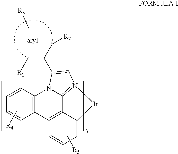
R1 and R2 are independently selected from the group consisting of hydrogen, alkyl, and aryl. At least one of R1 and R2 is an alkyl having four or more atoms. R3, R4, and R5 may represent mono, di, tri, or tetra substitutions. R3, R4, and R5 are independently selected from the group consisting of hydrogen, alkyl, and aryl. In one aspect, R1 and R2 are the same. In another aspect, R1 and R2 are different. In yet another aspect, one of R1 and R2 is an aryl.


R1 and R2 are independently selected from the group consisting of hydrogen, alkyl, and aryl, and at least one of R1 and R2 is an alkyl having four or more atoms. R3, R4, and R5 may represent mono, di, tri, or tetra substitutions. R3, R4, and R5 are independently selected from the group consisting of hydrogen, alkyl, and aryl.

where R1 and R2 are independently selected from the group consisting of hydrogen, alkyl, and aryl, and at least one of R1 and R2 is an alkyl having four or more atoms. R3, R4, and R5 may represent mono, di, tri, or tetra substitutions, and R3, R4, and R5 are independently selected from the group consisting of hydrogen, alkyl, and aryl. In one aspect, R1 and R2 are the same. In another aspect, R1 and R2 are different. In yet another aspect, one of R1 and R2 is an aryl.


R1 and R2 are independently selected from the group consisting of hydrogen, alkyl, and aryl, and at least one of R1 and R2 is an alkyl having four or more atoms. R3, R4, and R5 may represent mono, di, tri, or tetra substitutions. R3; R4, and R5 are independently selected from the group consisting of hydrogen, alkyl, and aryl. The dashed lines represent attachment of the ligand to a metal. Metals consisting of the non-radioactive metals with atomic numbers greater than 40 may be suitable for use in the complex. For example, the complex may include a metal selected from the group consisting of Re, Ru, Os, Rh, Ir, Pd, Pt, Cu and Au. Preferably, the metal is Ir. Moreover, the complex including the ligand provided may be a homoleptic complex or a heteroleptic complex. Preferably, the complex containing the ligand provided is a tris Ir complex.


wherein each of R1 through R6 are independently selected from the group consisting of any alkyl, alkoxy, amino, alkenyl, alkynyl, arylkyl, aryl, heteroaryl and hydrogen, and where each of R1 through R6 may represent multiple substitutions.
| TABLE 1 | ||
| MATERIAL | EXAMPLES OF MATERIAL | PUBLICATIONS |
| Hole injection materials | ||
| Phthalocyanine and porphryin compounds |
 |
Appl. Phys. Lett. 69, 2160 (1996) |
| Starburst triarylamines |
 |
J. Lumin. 72-74, 985 (1997) |
| CFx Fluorohydrocarbon polymer |
|
Appl. Phys. Lett. 78, 673 (2001) |
| Conducting polymers (e.g., PEDOT:PSS, polyaniline, polypthiophene) |
 |
Synth. Met. 87, 171 (1997) |
| Arylamines complexed with metal oxides such as molybdenum and tungsten oxides |
 |
SID Symposium Digest, 37, 923 (2006) |
| Hole transporting materials | ||
| Triarylamines (e.g., TPD, α-NPD) |
 |
Appl. Phys. Lett. 51, 913 (1987) |
 |
U.S. Pat. No. 5,061,569 | |
 |
EP650955 | |
 |
J. Mater. Chem. 3, 319 (1993) | |
 |
Appl. Phys. Lett. 90, 183503 (2007) | |
 |
Appl. Phys. Lett. 90, 183503 (2007) | |
| Triaylamine on spirofluorene core |
 |
Synth. Met. 91, 209 (1997) |
| Arylamine carbazole compounds |
 |
Adv. Mater. 6, 677 (1994) |
| Indolocarbazoles |
 |
Synth. Met. 111, 421 (2000) |
| Isoindole compounds |
 |
Chem. Mater. 15, 3148 (2003) |
| Phosphorescent OLED host | ||
| materials | ||
| Red hosts | ||
| Arylcarbazoles |
 |
Appl. Phys. Lett. 78, 1622 (2001) |
| Metal 8-hydroxyquinolates (e.g., Alq3, BAlq) |
 |
Nature 395, 151 (1998) |
 |
US20060202194 | |
 |
WO2005014551 | |
| Metal phenoxybenzothiazole compounds |
 |
Appl. Phys. Lett. 90, 123509 (2007) |
| Conjugated oligomers and polymers (e.g., polyfluorene) |
 |
Org. Electron. 1, 15 (2000) |
| Green hosts | ||
| Arylcarbazoles |
 |
Appl. Phys. Lett. 78, 1622 (2001) |
 |
US2003175553 | |
 |
WO2001039234 | |
| Aryltriphenylene compounds |
 |
US20060280965 |
 |
US20060280965 | |
| Polymers (e.g., PVK) |
 |
Appl. Phys. Lett. 77, 2280 (2000) |
| Spirofluorene compounds |
 |
WO2004093207 |
| Metal phenoxybenzooxazole compounds |
 |
WO05089025 |
 |
WO06132173 | |
 |
JP200511610 | |
| Spirofluorene-carbazole compounds |
 |
JP2007254297 |
 |
JP2007254297 | |
| Indolocabazoles |
 |
WO07063796 |
 |
WO07063754 | |
| 5-member ring electron deficient heterocycles (e.g., triazole, oxadiazole) |
 |
J. Appl. Phys. 90, 5048 (2001) |
 |
WO04107822 | |
| Metal phenoxypyridine compounds |
 |
WO05030900 |
| Blue Hosts | ||
| Arylcarbazoles |
 |
Appl. Phys. Lett, 82, 2422 (2003) |
 |
US20070190359 | |
| Dibenzothiophene-carbazole compounds |
 |
WO2006114966 |
| Phosphorescent dopants | ||
| Red dopants | ||
| Heavy metal porphyrins (e.g., PtOEP) |
 |
Nature 395, 151 (1998) |
| Iridium(III) organometallic complexes |
 |
Appl. Phys. Lett. 78, 1622 (2001) |
 |
U.S. Pat. No. 6,835,469 | |
 |
U.S. Pat. No. 6,835,469 | |
 |
US20060202194 | |
 |
US20060202194 | |
 |
U.S. Pat. No. 7,087,321 | |
 |
U.S. Pat. No. 7,087,321 | |
 |
Adv. Mater. 19, 739 (2007) | |
| Platinum(II) organometallic complexes |
 |
WO2003040257 |
| Osminum(III) complexes |
 |
Chem. Mater. 17, 3532 (2005) |
| Ruthenium(II) complexes |
 |
Adv. Mater. 17, 1059 (2005) |
| Green dopants | ||
| Iridium(III) organometallic complexes |
 |
Inorg. Chem. 40, 1704 (2001) |
 |
US2002034656 | |
 |
U.S. Pat. No. 06,687,266 | |
 |
Chem. Mater. 16, 2480 (2004) | |
 |
US2007190359 | |
 |
US 2006008670 JP2007123392 | |
 |
Adv. Mater. 16, 2003 (2004) | |
 |
Angew. Chem. Int. Ed. 2006, 45, 7800 | |
| Pt(II) organometallic complexes |
 |
Appl. Phys. Lett. 86, 153505 (2005) |
 |
Appl. Phys. Lett. 86, 153505 (2005) | |
 |
Chem. Lett. 34, 592 (2005) | |
| Gold complexes |
 |
Chem. Commun. 2906 (2005) |
| Rhenium(III) complexes |
 |
Inorg. Chem. 42, 1248 (2003) |
| Blue dopants | ||
| Iridium(III) organometallic complexes |
 |
WO2002002714 |
 |
WO2006009024 | |
 |
US2006251923 | |
 |
WO2006056418, US2005260441 | |
 |
US2007190359 | |
 |
US2002134984 | |
 |
Angew. Chem. Int. Ed. 47, 1 (2008) | |
 |
Chem. Mater. 18, 5119 (2006) | |
 |
Inorg. Chem. 46, 4308 (2007) | |
 |
WO05123873 | |
 |
WO05123873 | |
 |
WO07004380 | |
 |
WO06082742 | |
| Osmium(II) complexes |
 |
US2005260449 |
 |
Organometallics 23, 3745 (2004) | |
| Gold complexes |
 |
Appl. Phys. Lett. 74, 1361 (1999) |
| Platinum(II) complexes |
 |
WO06098120, WO06103874 |
| Exciton/hole blocking layer | ||
| materials | ||
| Bathocuprine compounds (e.g., BCP, BPhen) |
 |
Appl. Phys. Lett. 75, 4 (1999) |
 |
Appl. Phys. Lett. 79, 449 (2001) | |
| Metal 8-hydroxyquinolates (e.g., BAlq) |
 |
Appl. Phys. Lett. 81, 162 (2002) |
| 5-member ring electron deficient heterocycles such as triazole, oxadiazole, imidazole, benzoimidazole |
 |
Appl. Phys. Lett. 81, 162 (2002) |
| Triphenylene compounds |
 |
US20050025993 |
| Fluorinated aromatic compounds |
 |
Appl. Phys. Lett. 79, 156 (2001) |
| Electron transporting materials | ||
| Anthracene-benzoimidazole compounds |
 |
WO03060956 |
| Anthracene-benzothiazole compounds |
 |
Appl. Phys. Lett. 89, 063504 (2006) |
| Metal 8-hydroxyquinolates (e.g., Alq3) |
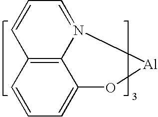 |
Appl. Phys. Lett. 51, 913 (1987) |
| Metal hydroxybenoquinolates |
 |
Chem. Lett. 5, 905 (1993) |
| Bathocuprine compounds such as BCP, BPhen, etc |
 |
Appl. Phys. Lett. 91, 263503 (2007) |
 |
Appl. Phys. Lett. 79, 449 (2001) | |
| 5-member ring electron deficient heterocycles (e.g., triazole, oxadiazole, imidazole, benzoimidazole) |
 |
Appl. Phys. Lett. 74, 865 (1999) |
 |
Appl. Phys. Lett. 55, 1489 (1989) | |
 |
Jpn. J. Apply. Phys. 32, L917 (1993) | |
| Silole compounds |
 |
Org. Electron. 4, 113 (2003) |
| Arylborane compounds |
 |
J. Am. Chem. Soc. 120, 9714 (1998) |
| Fluorinated aromatic compounds |
 |
J. Am. Chem. Soc. 122, 1832 (2000) |


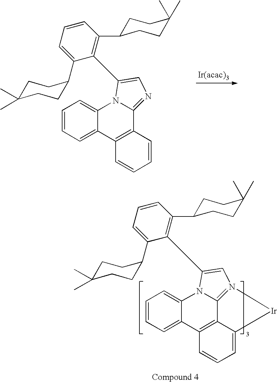

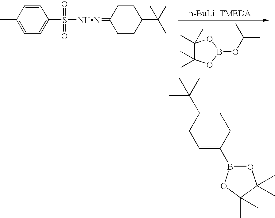


| TABLE 2 | ||||||||||
| EQE (%) | V (V) | T1/2 (h) | ||||||||
| Device | Emitter | at 1000 | at 1000 | at 2000 | Sublimation | |||||
| Example | (doping %) | cd/m2 | cd/m2 | cd/m2 | CIE | temp. (° C.) | HIL | HOST | ETL2 | PL % |
| Comparative | E1 | (9) | 12 | 8 | 70 | 0.15, 0.23 | 330 | H3 | H1 | H1 | 52 |
| 1 | |||||||||||
| Comparative | E2 | (9) | 7 | 8 | 200 | 0.15, 0.24 | 300 | H4 | H1 | H1 | 26 |
| 2 | |||||||||||
| Comparative | E3 | (9) | 8 | 8 | 180 | 0.15, 0.26 | 320 | H4 | H1 | H1 | 40 |
| 3 | |||||||||||
| 1 | 1 | (9) | 12 | 7 | 200 | 0.15, 0.24 | 265 | H3 | H2 | H2 | 56 |
| 2 | 2 | (9) | 12 | 8 | 300 | 0.15, 0.23 | 310 | H4 | H2 | H2 | 60 |
Claims (16)


Priority Applications (14)
| Application Number | Priority Date | Filing Date | Title |
|---|---|---|---|
| US12/632,251 US8815415B2 (en) | 2008-12-12 | 2009-12-07 | Blue emitter with high efficiency based on imidazo[1,2-f] phenanthridine iridium complexes |
| JP2011540925A JP6258570B2 (en) | 2008-12-12 | 2009-12-11 | Blue emitter with high efficiency based on imidazo [1,2-f] phenanthridine iridium complex |
| CN201410120954.6A CN103896991B (en) | 2008-12-12 | 2009-12-11 | Efficient blue light-emitting body is had based on imidazo [1,2 f] phenanthridines complex of iridium |
| EP16166849.6A EP3081617B1 (en) | 2008-12-12 | 2009-12-11 | Blue emitter with high efficiency based on imidazo [1,2-f] phenanthridine iridium complexes |
| TW104112487A TWI580680B (en) | 2008-12-12 | 2009-12-11 | Blue emitter with high efficiency based on imidazo[1,2-f]phenanthridine iridium complexes |
| EP09796526.3A EP2382281B1 (en) | 2008-12-12 | 2009-12-11 | BLUE EMITTER WITH HIGH EFFICIENCY BASED ON IMIDAZO [1,2-f] PHENANTHRIDINE IRIDIUM COMPLEXES |
| TW098142607A TWI492945B (en) | 2008-12-12 | 2009-12-11 | Blue emitter with high efficiency based on imidazo(1,2-f)phenanthridine iridium complexes |
| CN200980155336.2A CN102292409B (en) | 2008-12-12 | 2009-12-11 | High-efficiency blue light emitters based on imidazo[1,2-f]phenanthridine iridium complexes |
| PCT/US2009/067687 WO2010068876A1 (en) | 2008-12-12 | 2009-12-11 | BLUE EMITTER WITH HIGH EFFICIENCY BASED ON IMIDAZO [1,2-f] PHENANTHRIDINE IRIDIUM COMPLEXES |
| KR1020117016181A KR101636100B1 (en) | 2008-12-12 | 2009-12-11 | BLUE EMITTER WITH HIGH EFFICIENCY BASED ON IMIDAZO [1,2-f] PHENANTHRIDINE IRIDIUM COMPLEXES |
| US14/330,351 US10008678B2 (en) | 2008-12-12 | 2014-07-14 | Organic electroluminescent materials and devices |
| JP2016100224A JP6506211B2 (en) | 2008-12-12 | 2016-05-19 | Blue emitter with high efficiency based on imidazo [1,2-f] phenanthridine iridium complex |
| JP2017195003A JP6586140B2 (en) | 2008-12-12 | 2017-10-05 | Blue emitter with high efficiency based on imidazo [1,2-f] phenanthridine iridium complex |
| JP2019100281A JP6763999B2 (en) | 2008-12-12 | 2019-05-29 | Highly efficient blue illuminant based on imidazole [1,2-f] phenanthridine iridium complex |
Applications Claiming Priority (2)
| Application Number | Priority Date | Filing Date | Title |
|---|---|---|---|
| US12225908P | 2008-12-12 | 2008-12-12 | |
| US12/632,251 US8815415B2 (en) | 2008-12-12 | 2009-12-07 | Blue emitter with high efficiency based on imidazo[1,2-f] phenanthridine iridium complexes |
Related Child Applications (1)
| Application Number | Title | Priority Date | Filing Date |
|---|---|---|---|
| US14/330,351 Continuation US10008678B2 (en) | 2008-12-12 | 2014-07-14 | Organic electroluminescent materials and devices |
Publications (2)
| Publication Number | Publication Date |
|---|---|
| US20100148663A1 US20100148663A1 (en) | 2010-06-17 |
| US8815415B2 true US8815415B2 (en) | 2014-08-26 |
Family
ID=42239674
Family Applications (2)
| Application Number | Title | Priority Date | Filing Date |
|---|---|---|---|
| US12/632,251 Active 2031-07-07 US8815415B2 (en) | 2008-12-12 | 2009-12-07 | Blue emitter with high efficiency based on imidazo[1,2-f] phenanthridine iridium complexes |
| US14/330,351 Active 2032-06-17 US10008678B2 (en) | 2008-12-12 | 2014-07-14 | Organic electroluminescent materials and devices |
Family Applications After (1)
| Application Number | Title | Priority Date | Filing Date |
|---|---|---|---|
| US14/330,351 Active 2032-06-17 US10008678B2 (en) | 2008-12-12 | 2014-07-14 | Organic electroluminescent materials and devices |
Country Status (7)
| Country | Link |
|---|---|
| US (2) | US8815415B2 (en) |
| EP (2) | EP2382281B1 (en) |
| JP (4) | JP6258570B2 (en) |
| KR (1) | KR101636100B1 (en) |
| CN (2) | CN102292409B (en) |
| TW (2) | TWI580680B (en) |
| WO (1) | WO2010068876A1 (en) |
Cited By (6)
| Publication number | Priority date | Publication date | Assignee | Title |
|---|---|---|---|---|
| US20100141126A1 (en) * | 2007-05-16 | 2010-06-10 | Konica Minolta Holdings, Inc. | Organic electroluminescent element, display and illuminating device |
| US20140319504A1 (en) * | 2008-12-12 | 2014-10-30 | Universal Display Corporation | Organic electroluminescent materials and devices |
| US20160372668A1 (en) * | 2014-12-17 | 2016-12-22 | Universal Display Corporation | Organic electroluminescent materials and devices |
| US20170077426A1 (en) * | 2015-09-03 | 2017-03-16 | Universal Display Corporation | Organic electroluminescent materials and devices |
| US10017691B2 (en) | 2007-05-16 | 2018-07-10 | Konica Minolta, Inc. | Organic electroluminescent element, display device and lighting device |
| US10367160B2 (en) | 2011-03-23 | 2019-07-30 | Semiconductor Energy Laboratory Co., Ltd. | Light-emitting element |
Families Citing this family (145)
| Publication number | Priority date | Publication date | Assignee | Title |
|---|---|---|---|---|
| KR101600624B1 (en) | 2006-02-10 | 2016-03-21 | 유니버셜 디스플레이 코포레이션 | METAL COMPLEXES OF CYCLOMETALLATED IMIDAZO[1,2-f]PHENANTHRIDINE AND DIIMIDAZO[1,2-A:1',2'-C]QUINAZOLINE LIGANDS AND ISOELECTRONIC AND BENZANNULATED ANALOGS THEREOF |
| JP5531446B2 (en) * | 2009-04-20 | 2014-06-25 | コニカミノルタ株式会社 | ORGANIC ELECTROLUMINESCENT ELEMENT, ORGANIC ELECTROLUMINESCENT ELEMENT MATERIAL, DISPLAY DEVICE AND LIGHTING DEVICE |
| JP5568889B2 (en) * | 2009-05-22 | 2014-08-13 | コニカミノルタ株式会社 | ORGANIC ELECTROLUMINESCENT ELEMENT, DISPLAY DEVICE, LIGHTING DEVICE, AND ORGANIC ELECTROLUMINESCENT ELEMENT MATERIAL |
| US8993754B2 (en) | 2009-08-27 | 2015-03-31 | National Institute Of Advanced Industrial Science And Technology | Iridium complex and light emitting material formed from same |
| US8288187B2 (en) | 2010-01-20 | 2012-10-16 | Universal Display Corporation | Electroluminescent devices for lighting applications |
| US9175211B2 (en) * | 2010-03-03 | 2015-11-03 | Universal Display Corporation | Phosphorescent materials |
| CN103476781B (en) * | 2011-02-23 | 2017-02-15 | 通用显示公司 | Novel tetradentate platinum complexes |
| US9783564B2 (en) * | 2011-07-25 | 2017-10-10 | Universal Display Corporation | Organic electroluminescent materials and devices |
| TWI465441B (en) | 2011-08-12 | 2014-12-21 | Ind Tech Res Inst | Imidazole derivatives having vinyl group and its use in electroluminescent element |
| JP5742586B2 (en) * | 2011-08-25 | 2015-07-01 | コニカミノルタ株式会社 | Organic electroluminescence element, lighting device and display device |
| KR20140075012A (en) | 2011-10-19 | 2014-06-18 | 이 아이 듀폰 디 네모아 앤드 캄파니 | Organic electronic device for lighting |
| KR102012047B1 (en) | 2012-01-06 | 2019-08-19 | 유니버셜 디스플레이 코포레이션 | Highly efficient phosphorescent materials |
| US9224962B2 (en) * | 2012-03-01 | 2015-12-29 | The University Of Hong Kong | Dendrimers containing luminescent gold (III) compounds for organic light-emitting devices and their preparation |
| US9386657B2 (en) | 2012-03-15 | 2016-07-05 | Universal Display Corporation | Organic Electroluminescent materials and devices |
| US9540329B2 (en) | 2012-07-19 | 2017-01-10 | Universal Display Corporation | Organic electroluminescent materials and devices |
| US9663544B2 (en) * | 2012-07-25 | 2017-05-30 | Universal Display Corporation | Organic electroluminescent materials and devices |
| KR102127406B1 (en) | 2012-09-20 | 2020-06-29 | 유디씨 아일랜드 리미티드 | Azadibenzofurans for electronic applications |
| US9252363B2 (en) | 2012-10-04 | 2016-02-02 | Universal Display Corporation | Aryloxyalkylcarboxylate solvent compositions for inkjet printing of organic layers |
| US9196860B2 (en) | 2012-12-04 | 2015-11-24 | Universal Display Corporation | Compounds for triplet-triplet annihilation upconversion |
| US8716484B1 (en) | 2012-12-05 | 2014-05-06 | Universal Display Corporation | Hole transporting materials with twisted aryl groups |
| EP2744004B1 (en) * | 2012-12-11 | 2019-02-27 | Nissan Chemical Corporation | Process for the manufacture of a multilayer structure |
| US9653691B2 (en) | 2012-12-12 | 2017-05-16 | Universal Display Corporation | Phosphorescence-sensitizing fluorescence material system |
| US10400163B2 (en) | 2013-02-08 | 2019-09-03 | Universal Display Corporation | Organic electroluminescent materials and devices |
| KR102164633B1 (en) | 2013-03-20 | 2020-10-13 | 유디씨 아일랜드 리미티드 | Azabenzimidazole carbene complexes as efficiency booster in oleds |
| US20160372687A1 (en) | 2013-07-02 | 2016-12-22 | Basf Se | Monosubstituted diazabenzimidazole carbene metal complexes for use in organic light emitting diodes |
| CN109021022B (en) | 2013-07-31 | 2021-04-16 | Udc 爱尔兰有限责任公司 | Luminescent diazabenzimidazole carbene metal complexes |
| WO2015063046A1 (en) | 2013-10-31 | 2015-05-07 | Basf Se | Azadibenzothiophenes for electronic applications |
| US9876173B2 (en) | 2013-12-09 | 2018-01-23 | Universal Display Corporation | Organic electroluminescent materials and devices |
| US10347851B2 (en) | 2013-12-20 | 2019-07-09 | Udc Ireland Limited | Highly efficient OLED devices with very short decay times |
| CN115160373A (en) | 2014-03-31 | 2022-10-11 | Udc 爱尔兰有限责任公司 | Metal complexes and their use in organic light-emitting diodes |
| US9450198B2 (en) | 2014-04-15 | 2016-09-20 | Universal Display Corporation | Organic electroluminescent materials and devices |
| US10636983B2 (en) | 2014-05-08 | 2020-04-28 | Universal Display Corporation | Organic electroluminescent materials and devices |
| EP3473635B1 (en) * | 2014-05-08 | 2020-07-22 | Universal Display Corporation | Stabilized imidazophenanthridine materials |
| EP3174885B1 (en) | 2014-07-28 | 2019-10-02 | Idemitsu Kosan Co., Ltd. | 2,9-functionalized benzimidazolo[1,2-a]benzimidazoles as hosts for organic light emitting diodes (oleds) |
| EP2982676B1 (en) | 2014-08-07 | 2018-04-11 | Idemitsu Kosan Co., Ltd. | Benzimidazo[2,1-B]benzoxazoles for electronic applications |
| EP2993215B1 (en) | 2014-09-04 | 2019-06-19 | Idemitsu Kosan Co., Ltd. | Azabenzimidazo[2,1-a]benzimidazoles for electronic applications |
| EP3015469B1 (en) | 2014-10-30 | 2018-12-19 | Idemitsu Kosan Co., Ltd. | 5-(benzimidazol-2-yl)benzimidazo[1,2-a]benzimidazoles for electronic applications |
| WO2016079667A1 (en) | 2014-11-17 | 2016-05-26 | Idemitsu Kosan Co., Ltd. | Indole derivatives for electronic applications |
| EP3034507A1 (en) | 2014-12-15 | 2016-06-22 | Idemitsu Kosan Co., Ltd | 1-functionalized dibenzofurans and dibenzothiophenes for organic light emitting diodes (OLEDs) |
| EP3034506A1 (en) | 2014-12-15 | 2016-06-22 | Idemitsu Kosan Co., Ltd | 4-functionalized carbazole derivatives for electronic applications |
| KR102381900B1 (en) | 2015-01-07 | 2022-04-01 | 삼성디스플레이 주식회사 | Organic light emitting diode display |
| EP3054498B1 (en) | 2015-02-06 | 2017-09-20 | Idemitsu Kosan Co., Ltd. | Bisimidazodiazocines |
| EP3053918B1 (en) | 2015-02-06 | 2018-04-11 | Idemitsu Kosan Co., Ltd. | 2-carbazole substituted benzimidazoles for electronic applications |
| US9929361B2 (en) | 2015-02-16 | 2018-03-27 | Universal Display Corporation | Organic electroluminescent materials and devices |
| EP3061759B1 (en) | 2015-02-24 | 2019-12-25 | Idemitsu Kosan Co., Ltd | Nitrile substituted dibenzofurans |
| US11056657B2 (en) | 2015-02-27 | 2021-07-06 | University Display Corporation | Organic electroluminescent materials and devices |
| EP3070144B1 (en) | 2015-03-17 | 2018-02-28 | Idemitsu Kosan Co., Ltd. | Seven-membered ring compounds |
| EP3072943B1 (en) | 2015-03-26 | 2018-05-02 | Idemitsu Kosan Co., Ltd. | Dibenzofuran/carbazole-substituted benzonitriles |
| EP3075737B1 (en) | 2015-03-31 | 2019-12-04 | Idemitsu Kosan Co., Ltd | Benzimidazolo[1,2-a]benzimidazole carrying aryl- or heteroarylnitril groups for organic light emitting diodes |
| US9859510B2 (en) | 2015-05-15 | 2018-01-02 | Universal Display Corporation | Organic electroluminescent materials and devices |
| US10418568B2 (en) | 2015-06-01 | 2019-09-17 | Universal Display Corporation | Organic electroluminescent materials and devices |
| WO2016193243A1 (en) | 2015-06-03 | 2016-12-08 | Udc Ireland Limited | Highly efficient oled devices with very short decay times |
| US11127905B2 (en) | 2015-07-29 | 2021-09-21 | Universal Display Corporation | Organic electroluminescent materials and devices |
| EP3150606B1 (en) | 2015-10-01 | 2019-08-14 | Idemitsu Kosan Co., Ltd. | Benzimidazolo[1,2-a]benzimidazoles carrying benzofurane or benzothiophene groups for organic light emitting diodes |
| EP3150604B1 (en) | 2015-10-01 | 2021-07-14 | Idemitsu Kosan Co., Ltd. | Benzimidazolo[1,2-a]benzimidazole carrying benzimidazolo[1,2-a]benzimidazolylyl groups, carbazolyl groups, benzofurane groups or benzothiophene groups for organic light emitting diodes |
| EP3356369B1 (en) | 2015-10-01 | 2022-05-04 | Idemitsu Kosan Co., Ltd | Benzimidazolo[1,2-a]benzimidazole carrying triazine groups for organic light emitting diodes |
| US20180291028A1 (en) | 2015-10-01 | 2018-10-11 | Idemitsu Kosan Co., Ltd. | Benzimidazolo[1,2-a]benzimidazole carrying benzimidazolo[1,2-a]benzimidazolyl groups, carbazolyl groups, benzofurane groups or benzothiophene groups for organic light emitting diodes |
| WO2017078182A1 (en) | 2015-11-04 | 2017-05-11 | Idemitsu Kosan Co., Ltd. | Benzimidazole fused heteroaryls |
| WO2017093958A1 (en) | 2015-12-04 | 2017-06-08 | Idemitsu Kosan Co., Ltd. | Benzimidazolo[1,2-a]benzimidazole derivatives for organic light emitting diodes |
| US20170229663A1 (en) | 2016-02-09 | 2017-08-10 | Universal Display Corporation | Organic electroluminescent materials and devices |
| US10236456B2 (en) | 2016-04-11 | 2019-03-19 | Universal Display Corporation | Organic electroluminescent materials and devices |
| WO2017178864A1 (en) | 2016-04-12 | 2017-10-19 | Idemitsu Kosan Co., Ltd. | Seven-membered ring compounds |
| US11482683B2 (en) | 2016-06-20 | 2022-10-25 | Universal Display Corporation | Organic electroluminescent materials and devices |
| US10672997B2 (en) | 2016-06-20 | 2020-06-02 | Universal Display Corporation | Organic electroluminescent materials and devices |
| US10862054B2 (en) | 2016-06-20 | 2020-12-08 | Universal Display Corporation | Organic electroluminescent materials and devices |
| US10608186B2 (en) | 2016-09-14 | 2020-03-31 | Universal Display Corporation | Organic electroluminescent materials and devices |
| US10680187B2 (en) | 2016-09-23 | 2020-06-09 | Universal Display Corporation | Organic electroluminescent materials and devices |
| US11196010B2 (en) | 2016-10-03 | 2021-12-07 | Universal Display Corporation | Organic electroluminescent materials and devices |
| US11011709B2 (en) | 2016-10-07 | 2021-05-18 | Universal Display Corporation | Organic electroluminescent materials and devices |
| US12317745B2 (en) | 2016-11-09 | 2025-05-27 | Universal Display Corporation | Organic electroluminescent materials and devices |
| US10680188B2 (en) | 2016-11-11 | 2020-06-09 | Universal Display Corporation | Organic electroluminescent materials and devices |
| CN110088115B (en) * | 2016-12-16 | 2024-05-14 | 株式会社半导体能源研究所 | Organometallic complex, light-emitting element, light-emitting device, electronic device, and lighting device |
| US11780865B2 (en) | 2017-01-09 | 2023-10-10 | Universal Display Corporation | Organic electroluminescent materials and devices |
| US10844085B2 (en) | 2017-03-29 | 2020-11-24 | Universal Display Corporation | Organic electroluminescent materials and devices |
| US10944060B2 (en) | 2017-05-11 | 2021-03-09 | Universal Display Corporation | Organic electroluminescent materials and devices |
| US12098157B2 (en) | 2017-06-23 | 2024-09-24 | Universal Display Corporation | Organic electroluminescent materials and devices |
| US11228010B2 (en) | 2017-07-26 | 2022-01-18 | Universal Display Corporation | Organic electroluminescent materials and devices |
| US11744142B2 (en) | 2017-08-10 | 2023-08-29 | Universal Display Corporation | Organic electroluminescent materials and devices |
| US12180230B2 (en) | 2017-11-28 | 2024-12-31 | University Of Southern California | Carbene compounds and organic electroluminescent devices |
| EP3492480B1 (en) | 2017-11-29 | 2021-10-20 | Universal Display Corporation | Organic electroluminescent materials and devices |
| US11937503B2 (en) | 2017-11-30 | 2024-03-19 | Universal Display Corporation | Organic electroluminescent materials and devices |
| US11542289B2 (en) | 2018-01-26 | 2023-01-03 | Universal Display Corporation | Organic electroluminescent materials and devices |
| US11165028B2 (en) | 2018-03-12 | 2021-11-02 | Universal Display Corporation | Organic electroluminescent materials and devices |
| US12453279B2 (en) | 2018-08-22 | 2025-10-21 | Universal Display Corporation | Organic electroluminescent materials and devices |
| TWI826522B (en) | 2018-09-12 | 2023-12-21 | 德商麥克專利有限公司 | Electroluminescent devices |
| TW202030902A (en) | 2018-09-12 | 2020-08-16 | 德商麥克專利有限公司 | Electroluminescent devices |
| WO2020053150A1 (en) | 2018-09-12 | 2020-03-19 | Merck Patent Gmbh | Materials for organic electroluminescent devices |
| US11737349B2 (en) | 2018-12-12 | 2023-08-22 | Universal Display Corporation | Organic electroluminescent materials and devices |
| US11780829B2 (en) | 2019-01-30 | 2023-10-10 | The University Of Southern California | Organic electroluminescent materials and devices |
| US12477890B2 (en) | 2019-02-01 | 2025-11-18 | Universal Display Corporation | Organic electroluminescent materials and devices |
| US20220127286A1 (en) | 2019-03-04 | 2022-04-28 | Merck Patent Gmbh | Ligands for nano-sized materials |
| JP2020158491A (en) | 2019-03-26 | 2020-10-01 | ユニバーサル ディスプレイ コーポレイション | Organic electroluminescent materials and devices |
| KR102769410B1 (en) | 2019-04-11 | 2025-02-17 | 메르크 파텐트 게엠베하 | Materials for organic electroluminescent devices |
| US11560398B2 (en) * | 2019-05-07 | 2023-01-24 | Universal Display Corporation | Organic electroluminescent materials and devices |
| CN112010881B (en) * | 2019-05-30 | 2021-09-03 | 中国科学院兰州化学物理研究所 | Alkenyl boron compound and preparation method and application thereof |
| US12281128B2 (en) | 2019-07-30 | 2025-04-22 | Universal Display Corporation | Organic electroluminescent materials and devices |
| US12139501B2 (en) | 2019-08-16 | 2024-11-12 | Universal Display Corporation | Organic electroluminescent materials and devices |
| US20210135130A1 (en) | 2019-11-04 | 2021-05-06 | Universal Display Corporation | Organic electroluminescent materials and devices |
| US20230002416A1 (en) | 2019-11-04 | 2023-01-05 | Merck Patent Gmbh | Materials for organic electroluminescent devices |
| TW202134252A (en) | 2019-11-12 | 2021-09-16 | 德商麥克專利有限公司 | Materials for organic electroluminescent devices |
| TW202136181A (en) | 2019-12-04 | 2021-10-01 | 德商麥克專利有限公司 | Materials for organic electroluminescent devices |
| US20210217969A1 (en) | 2020-01-06 | 2021-07-15 | Universal Display Corporation | Organic electroluminescent materials and devices |
| US12426495B2 (en) | 2020-01-28 | 2025-09-23 | Universal Display Corporation | Organic electroluminescent materials and devices |
| KR20220133937A (en) | 2020-01-29 | 2022-10-05 | 메르크 파텐트 게엠베하 | Benzimidazole derivatives |
| CN115244060A (en) | 2020-03-23 | 2022-10-25 | 默克专利有限公司 | Material for organic electroluminescent device |
| EP3937268B1 (en) | 2020-07-10 | 2025-05-07 | Universal Display Corporation | Plasmonic oleds and vertical dipole emitters |
| KR102867203B1 (en) | 2020-07-13 | 2025-10-16 | 삼성디스플레이 주식회사 | Light emitting device, electronic apparatus including the same and organometallic compound |
| KR20230077725A (en) | 2020-09-18 | 2023-06-01 | 삼성디스플레이 주식회사 | organic electroluminescent device |
| US12187748B2 (en) | 2020-11-02 | 2025-01-07 | Universal Display Corporation | Organic electroluminescent materials and devices |
| US20220158096A1 (en) | 2020-11-16 | 2022-05-19 | Universal Display Corporation | Organic electroluminescent materials and devices |
| US12325717B2 (en) | 2020-11-24 | 2025-06-10 | Universal Display Corporation | Organic electroluminescent materials and devices |
| US20220165967A1 (en) | 2020-11-24 | 2022-05-26 | Universal Display Corporation | Organic electroluminescent materials and devices |
| US20220271241A1 (en) | 2021-02-03 | 2022-08-25 | Universal Display Corporation | Organic electroluminescent materials and devices |
| EP4059915A3 (en) | 2021-02-26 | 2022-12-28 | Universal Display Corporation | Organic electroluminescent materials and devices |
| EP4060758A3 (en) | 2021-02-26 | 2023-03-29 | Universal Display Corporation | Organic electroluminescent materials and devices |
| US20220298192A1 (en) | 2021-03-05 | 2022-09-22 | Universal Display Corporation | Organic electroluminescent materials and devices |
| US12428599B2 (en) | 2021-03-09 | 2025-09-30 | Universal Display Corporation | Organic electroluminescent materials and devices |
| US20220298190A1 (en) | 2021-03-12 | 2022-09-22 | Universal Display Corporation | Organic electroluminescent materials and devices |
| US12421262B2 (en) | 2021-03-15 | 2025-09-23 | Universal Display Corporation | Organic electroluminescent materials and devices |
| US20220340607A1 (en) | 2021-04-05 | 2022-10-27 | Universal Display Corporation | Organic electroluminescent materials and devices |
| US12480042B2 (en) | 2021-04-09 | 2025-11-25 | Universal Display Corporation | Organic electroluminescent materials and devices |
| EP4075531A1 (en) | 2021-04-13 | 2022-10-19 | Universal Display Corporation | Plasmonic oleds and vertical dipole emitters |
| US20220352478A1 (en) | 2021-04-14 | 2022-11-03 | Universal Display Corporation | Organic eletroluminescent materials and devices |
| US20230006149A1 (en) | 2021-04-23 | 2023-01-05 | Universal Display Corporation | Organic electroluminescent materials and devices |
| US20220407020A1 (en) | 2021-04-23 | 2022-12-22 | Universal Display Corporation | Organic electroluminescent materials and devices |
| US20230133787A1 (en) | 2021-06-08 | 2023-05-04 | University Of Southern California | Molecular Alignment of Homoleptic Iridium Phosphors |
| EP4151699A1 (en) | 2021-09-17 | 2023-03-22 | Universal Display Corporation | Organic electroluminescent materials and devices |
| US12473318B2 (en) | 2021-10-08 | 2025-11-18 | Universal Display Corporation | Organic electroluminescent materials and devices |
| US20240343970A1 (en) | 2021-12-16 | 2024-10-17 | Universal Display Corporation | Organic electroluminescent materials and devices |
| EP4231804A3 (en) | 2022-02-16 | 2023-09-20 | Universal Display Corporation | Organic electroluminescent materials and devices |
| US20230292592A1 (en) | 2022-03-09 | 2023-09-14 | Universal Display Corporation | Organic electroluminescent materials and devices |
| US20230337516A1 (en) | 2022-04-18 | 2023-10-19 | Universal Display Corporation | Organic electroluminescent materials and devices |
| US20230389421A1 (en) | 2022-05-24 | 2023-11-30 | Universal Display Corporation | Organic electroluminescent materials and devices |
| EP4293001A1 (en) | 2022-06-08 | 2023-12-20 | Universal Display Corporation | Organic electroluminescent materials and devices |
| US20240016051A1 (en) | 2022-06-28 | 2024-01-11 | Universal Display Corporation | Organic electroluminescent materials and devices |
| US20240107880A1 (en) | 2022-08-17 | 2024-03-28 | Universal Display Corporation | Organic electroluminescent materials and devices |
| US20240196730A1 (en) | 2022-10-27 | 2024-06-13 | Universal Display Corporation | Organic electroluminescent materials and devices |
| US20240180025A1 (en) | 2022-10-27 | 2024-05-30 | Universal Display Corporation | Organic electroluminescent materials and devices |
| US20240188316A1 (en) | 2022-10-27 | 2024-06-06 | Universal Display Corporation | Organic electroluminescent materials and devices |
| US20240188419A1 (en) | 2022-10-27 | 2024-06-06 | Universal Display Corporation | Organic electroluminescent materials and devices |
| US20240188319A1 (en) | 2022-10-27 | 2024-06-06 | Universal Display Corporation | Organic electroluminescent materials and devices |
| CN120153045A (en) | 2022-11-17 | 2025-06-13 | 默克专利有限公司 | Materials for organic electroluminescent devices |
| US20240247017A1 (en) | 2022-12-14 | 2024-07-25 | Universal Display Corporation | Organic electroluminescent materials and devices |
| US20250204239A1 (en) | 2023-12-15 | 2025-06-19 | Universal Display Corporation | Organic electroluminescent materials and devices |
| US20250204238A1 (en) | 2023-12-15 | 2025-06-19 | Universal Display Corporation | Organic electroluminscent materials and devices |
Citations (57)
| Publication number | Priority date | Publication date | Assignee | Title |
|---|---|---|---|---|
| US4769292A (en) | 1987-03-02 | 1988-09-06 | Eastman Kodak Company | Electroluminescent device with modified thin film luminescent zone |
| US5061569A (en) | 1990-07-26 | 1991-10-29 | Eastman Kodak Company | Electroluminescent device with organic electroluminescent medium |
| US5247190A (en) | 1989-04-20 | 1993-09-21 | Cambridge Research And Innovation Limited | Electroluminescent devices |
| EP0650955A1 (en) | 1993-11-01 | 1995-05-03 | Hodogaya Chemical Co., Ltd. | Amine compound and electro-luminescence device comprising same |
| US5703436A (en) | 1994-12-13 | 1997-12-30 | The Trustees Of Princeton University | Transparent contacts for organic devices |
| US5707745A (en) | 1994-12-13 | 1998-01-13 | The Trustees Of Princeton University | Multicolor organic light emitting devices |
| US5834893A (en) | 1996-12-23 | 1998-11-10 | The Trustees Of Princeton University | High efficiency organic light emitting devices with light directing structures |
| US5844363A (en) | 1997-01-23 | 1998-12-01 | The Trustees Of Princeton Univ. | Vacuum deposited, non-polymeric flexible organic light emitting devices |
| US6013982A (en) | 1996-12-23 | 2000-01-11 | The Trustees Of Princeton University | Multicolor display devices |
| US6087196A (en) | 1998-01-30 | 2000-07-11 | The Trustees Of Princeton University | Fabrication of organic semiconductor devices using ink jet printing |
| US6091195A (en) | 1997-02-03 | 2000-07-18 | The Trustees Of Princeton University | Displays having mesa pixel configuration |
| US6097147A (en) | 1998-09-14 | 2000-08-01 | The Trustees Of Princeton University | Structure for high efficiency electroluminescent device |
| WO2001039234A2 (en) | 1999-11-24 | 2001-05-31 | The Trustees Of Princeton University | Organic light emitting diode having a blue phosphorescent molecule as an emitter |
| US6294398B1 (en) | 1999-11-23 | 2001-09-25 | The Trustees Of Princeton University | Method for patterning devices |
| US6303238B1 (en) | 1997-12-01 | 2001-10-16 | The Trustees Of Princeton University | OLEDs doped with phosphorescent compounds |
| US6337102B1 (en) | 1997-11-17 | 2002-01-08 | The Trustees Of Princeton University | Low pressure vapor phase deposition of organic thin films |
| WO2002002714A2 (en) | 2000-06-30 | 2002-01-10 | E.I. Du Pont De Nemours And Company | Electroluminescent iridium compounds with fluorinated phenylpyridines, phenylpyrimidines, and phenylquinolines and devices made with such compounds |
| US20020034656A1 (en) | 1998-09-14 | 2002-03-21 | Thompson Mark E. | Organometallic complexes as phosphorescent emitters in organic LEDs |
| US20020134984A1 (en) | 2001-02-01 | 2002-09-26 | Fuji Photo Film Co., Ltd. | Transition metal complex and light-emitting device |
| WO2003040257A1 (en) | 2001-11-07 | 2003-05-15 | E. I. Du Pont De Nemours And Company | Electroluminescent platinum compounds and devices made with such compounds |
| WO2003060956A2 (en) | 2002-01-18 | 2003-07-24 | Lg Chem, Ltd. | New material for transporting electrons and organic electroluminescent display using the same |
| US20030175553A1 (en) | 2001-12-28 | 2003-09-18 | Thompson Mark E. | White light emitting oleds from combined monomer and aggregate emission |
| US20030230980A1 (en) | 2002-06-18 | 2003-12-18 | Forrest Stephen R | Very low voltage, high efficiency phosphorescent oled in a p-i-n structure |
| US6687266B1 (en) | 2002-11-08 | 2004-02-03 | Universal Display Corporation | Organic light emitting materials and devices |
| US20040174116A1 (en) | 2001-08-20 | 2004-09-09 | Lu Min-Hao Michael | Transparent electrodes |
| WO2004093207A2 (en) | 2003-04-15 | 2004-10-28 | Covion Organic Semiconductors Gmbh | Mixtures of matrix materials and organic semiconductors capable of emission, use of the same and electronic components containing said mixtures |
| WO2004107822A1 (en) | 2003-05-29 | 2004-12-09 | Nippon Steel Chemical Co., Ltd. | Organic electroluminescent element |
| US6835469B2 (en) | 2001-10-17 | 2004-12-28 | The University Of Southern California | Phosphorescent compounds and devices comprising the same |
| JP2005011610A (en) | 2003-06-18 | 2005-01-13 | Nippon Steel Chem Co Ltd | Organic electroluminescence device |
| US20050025993A1 (en) | 2003-07-25 | 2005-02-03 | Thompson Mark E. | Materials and structures for enhancing the performance of organic light emitting devices |
| WO2005014551A1 (en) | 2003-08-07 | 2005-02-17 | Nippon Steel Chemical Co., Ltd. | Aluminum chelate compelx for organic el material |
| WO2005030900A1 (en) | 2003-09-25 | 2005-04-07 | Nippon Steel Chemical Co., Ltd. | Organic electroluminescent device |
| WO2005089025A1 (en) | 2004-03-15 | 2005-09-22 | Nippon Steel Chemical Co., Ltd. | Organic electroluminescent device |
| US20050260441A1 (en) | 2004-05-18 | 2005-11-24 | Thompson Mark E | Luminescent compounds with carbene ligands |
| US20050260449A1 (en) | 2004-05-18 | 2005-11-24 | Robert Walters | Complexes with tridentate ligands |
| WO2005123873A1 (en) | 2004-06-17 | 2005-12-29 | Konica Minolta Holdings, Inc. | Organic electroluminescent device material, organic electroluminescent device, display and illuminating device |
| US20060008670A1 (en) | 2004-07-06 | 2006-01-12 | Chun Lin | Organic light emitting materials and devices |
| WO2006009024A1 (en) | 2004-07-23 | 2006-01-26 | Konica Minolta Holdings, Inc. | Organic electroluminescent device, display and illuminating device |
| WO2006056418A2 (en) | 2004-11-25 | 2006-06-01 | Basf Aktiengesellschaft | Use of transition metal carbene complexes in organic light-emitting diodes (oleds) |
| US7087321B2 (en) | 2003-04-22 | 2006-08-08 | Universal Display Corporation | Organic light emitting devices having reduced pixel shrinkage |
| WO2006082742A1 (en) | 2005-02-04 | 2006-08-10 | Konica Minolta Holdings, Inc. | Organic electroluminescent device material, organic electroluminescent device, display and illuminating device |
| US20060202194A1 (en) | 2005-03-08 | 2006-09-14 | Jeong Hyun C | Red phosphorescene compounds and organic electroluminescence device using the same |
| WO2006098120A1 (en) | 2005-03-16 | 2006-09-21 | Konica Minolta Holdings, Inc. | Organic electroluminescent device material and organic electroluminescent device |
| WO2006103874A1 (en) | 2005-03-29 | 2006-10-05 | Konica Minolta Holdings, Inc. | Organic electroluminescent device material, organic electroluminescent device, display and illuminating device |
| WO2006114966A1 (en) | 2005-04-18 | 2006-11-02 | Konica Minolta Holdings, Inc. | Organic electroluminescent device, display and illuminating device |
| US20060251923A1 (en) | 2005-05-06 | 2006-11-09 | Chun Lin | Stability OLED materials and devices |
| WO2006132173A1 (en) | 2005-06-07 | 2006-12-14 | Nippon Steel Chemical Co., Ltd. | Organic metal complex and organic electroluminescent device using same |
| WO2007004380A1 (en) | 2005-07-01 | 2007-01-11 | Konica Minolta Holdings, Inc. | Organic electroluminescent element material, organic electroluminescent element, display device, and lighting equipment |
| JP2007123392A (en) | 2005-10-26 | 2007-05-17 | Konica Minolta Holdings Inc | Organic electroluminescence element, display device and lighting device |
| WO2007063796A1 (en) | 2005-12-01 | 2007-06-07 | Nippon Steel Chemical Co., Ltd. | Organic electroluminescent device |
| WO2007063754A1 (en) | 2005-12-01 | 2007-06-07 | Nippon Steel Chemical Co., Ltd. | Compound for organic electroluminescent element and organic electroluminescent element |
| US20070190359A1 (en) | 2006-02-10 | 2007-08-16 | Knowles David B | Metal complexes of cyclometallated imidazo[1,2-ƒ]phenanthridine and diimidazo[1,2-a:1',2'-c]quinazoline ligands and isoelectronic and benzannulated analogs thereof |
| JP2007254297A (en) | 2006-03-20 | 2007-10-04 | Nippon Steel Chem Co Ltd | Luminescent layer compound and organic electroluminescent device |
| WO2008140114A1 (en) | 2007-05-16 | 2008-11-20 | Konica Minolta Holdings, Inc. | Organic electroluminescence element, display device and illuminating device |
| WO2008142976A1 (en) | 2007-05-16 | 2008-11-27 | Konica Minolta Holdings, Inc. | Organic electroluminescence element, display device, illuminating device and organic electroluminescence element material |
| US20090121624A1 (en) * | 2007-11-09 | 2009-05-14 | Universal Display Corporation | Stable blue phosphorescent organic light emitting devices |
| US8142909B2 (en) * | 2006-02-10 | 2012-03-27 | Universal Display Corporation | Blue phosphorescent imidazophenanthridine materials |
Family Cites Families (83)
| Publication number | Priority date | Publication date | Assignee | Title |
|---|---|---|---|---|
| US6939625B2 (en) | 1996-06-25 | 2005-09-06 | Nôrthwestern University | Organic light-emitting diodes and methods for assembly and enhanced charge injection |
| US6528187B1 (en) | 1998-09-08 | 2003-03-04 | Fuji Photo Film Co., Ltd. | Material for luminescence element and luminescence element using the same |
| KR100377321B1 (en) | 1999-12-31 | 2003-03-26 | 주식회사 엘지화학 | Electronic device comprising organic compound having p-type semiconducting characteristics |
| EP2566302B1 (en) | 2000-08-11 | 2015-12-16 | The Trustees of Princeton University | Organometallic compounds and emission-shifting organic electrophosphorence |
| JP2002063988A (en) * | 2000-08-22 | 2002-02-28 | Toray Ind Inc | Light emitting element |
| JP4343528B2 (en) | 2000-11-30 | 2009-10-14 | キヤノン株式会社 | Light emitting element and display device |
| US6579630B2 (en) | 2000-12-07 | 2003-06-17 | Canon Kabushiki Kaisha | Deuterated semiconducting organic compounds used for opto-electronic devices |
| JP4307000B2 (en) | 2001-03-08 | 2009-08-05 | キヤノン株式会社 | Metal coordination compound, electroluminescent element and display device |
| JP4310077B2 (en) | 2001-06-19 | 2009-08-05 | キヤノン株式会社 | Metal coordination compound and organic light emitting device |
| US7396598B2 (en) | 2001-06-20 | 2008-07-08 | Showa Denko K.K. | Light emitting material and organic light-emitting device |
| US7250226B2 (en) | 2001-08-31 | 2007-07-31 | Nippon Hoso Kyokai | Phosphorescent compound, a phosphorescent composition and an organic light-emitting device |
| US7431968B1 (en) | 2001-09-04 | 2008-10-07 | The Trustees Of Princeton University | Process and apparatus for organic vapor jet deposition |
| JP2003101925A (en) | 2001-09-26 | 2003-04-04 | Alpine Electronics Inc | Disc playback device |
| US7189989B2 (en) | 2002-08-22 | 2007-03-13 | Fuji Photo Film Co., Ltd. | Light emitting element |
| KR100686268B1 (en) | 2002-08-27 | 2007-02-28 | 후지필름 가부시키가이샤 | Organometallic Complex, Organic EL Element, and Organic EL Display |
| ATE307840T1 (en) * | 2002-09-14 | 2005-11-15 | Merck Patent Gmbh | MONO-, OLIGO- AND POLY(3-ALKYNYLTHIOPHENES) AND THEIR USE AS CARGO TRANSPORT MATERIALS |
| JP4365199B2 (en) | 2002-12-27 | 2009-11-18 | 富士フイルム株式会社 | Organic electroluminescence device |
| JP4365196B2 (en) | 2002-12-27 | 2009-11-18 | 富士フイルム株式会社 | Organic electroluminescence device |
| US7090928B2 (en) | 2003-04-01 | 2006-08-15 | The University Of Southern California | Binuclear compounds |
| TWI287567B (en) | 2003-07-30 | 2007-10-01 | Chi Mei Optoelectronics Corp | Light-emitting element and iridium complex |
| DE10338550A1 (en) | 2003-08-19 | 2005-03-31 | Basf Ag | Transition metal complexes with carbene ligands as emitters for organic light-emitting diodes (OLEDs) |
| JP4822687B2 (en) | 2003-11-21 | 2011-11-24 | 富士フイルム株式会社 | Organic electroluminescence device |
| US7332232B2 (en) | 2004-02-03 | 2008-02-19 | Universal Display Corporation | OLEDs utilizing multidentate ligand systems |
| EP2325191A1 (en) | 2004-03-11 | 2011-05-25 | Mitsubishi Chemical Corporation | Composition for charge-transporting film and ion compound, charge-transporting film and organic electroluminescent device using same |
| JP4869565B2 (en) | 2004-04-23 | 2012-02-08 | 富士フイルム株式会社 | Organic electroluminescence device |
| US7154114B2 (en) | 2004-05-18 | 2006-12-26 | Universal Display Corporation | Cyclometallated iridium carbene complexes for use as hosts |
| US7534505B2 (en) | 2004-05-18 | 2009-05-19 | The University Of Southern California | Organometallic compounds for use in electroluminescent devices |
| US7393599B2 (en) | 2004-05-18 | 2008-07-01 | The University Of Southern California | Luminescent compounds with carbene ligands |
| US7445855B2 (en) | 2004-05-18 | 2008-11-04 | The University Of Southern California | Cationic metal-carbene complexes |
| US7820828B2 (en) | 2004-06-28 | 2010-10-26 | Ciba Specialty Chemicals Corp. | Electroluminescent metal complexes with triazoles and benzotriazoles |
| WO2006072002A2 (en) | 2004-12-30 | 2006-07-06 | E.I. Dupont De Nemours And Company | Organometallic complexes |
| DE102005014284A1 (en) | 2005-03-24 | 2006-09-28 | Basf Ag | Use of compounds containing aromatic or heteroaromatic rings containing groups via carbonyl groups as matrix materials in organic light-emitting diodes |
| US7807275B2 (en) | 2005-04-21 | 2010-10-05 | Universal Display Corporation | Non-blocked phosphorescent OLEDs |
| JP4533796B2 (en) | 2005-05-06 | 2010-09-01 | 富士フイルム株式会社 | Organic electroluminescence device |
| WO2006130598A2 (en) | 2005-05-31 | 2006-12-07 | Universal Display Corporation | Triphenylene hosts in phosphorescent light emitting diodes |
| KR101294905B1 (en) | 2005-06-27 | 2013-08-09 | 이 아이 듀폰 디 네모아 앤드 캄파니 | Electrically Conductive Polymer Compositions |
| WO2007028417A1 (en) | 2005-09-07 | 2007-03-15 | Technische Universität Braunschweig | Triplett emitter having condensed five-membered rings |
| JP4659695B2 (en) * | 2005-11-01 | 2011-03-30 | キヤノン株式会社 | Fluorene compound and organic light emitting device |
| WO2007097149A1 (en) * | 2006-02-20 | 2007-08-30 | Konica Minolta Holdings, Inc. | Organic electroluminescence element, white light emitting element, display device and illuminating device |
| JP2007284549A (en) * | 2006-04-17 | 2007-11-01 | Konica Minolta Holdings Inc | Organic electroluminescent element material, organic electroluminescent element, display and lighting apparatus |
| WO2007125714A1 (en) | 2006-04-26 | 2007-11-08 | Idemitsu Kosan Co., Ltd. | Aromatic amine derivative, and organic electroluminescence element using the same |
| KR101384046B1 (en) | 2006-05-11 | 2014-04-09 | 이데미쓰 고산 가부시키가이샤 | Organic electroluminescent device |
| WO2007142083A1 (en) | 2006-06-02 | 2007-12-13 | Idemitsu Kosan Co., Ltd. | Material for organic electroluminescence element, and organic electroluminescence element using the material |
| JPWO2008016018A1 (en) * | 2006-08-04 | 2009-12-24 | 出光興産株式会社 | Material for organic electroluminescence device and organic electroluminescence device using the same |
| KR20090040895A (en) | 2006-08-23 | 2009-04-27 | 이데미쓰 고산 가부시키가이샤 | Aromatic amine derivatives and organic electroluminescent devices using them |
| JP5589251B2 (en) | 2006-09-21 | 2014-09-17 | コニカミノルタ株式会社 | Organic electroluminescence element material |
| JP5245105B2 (en) * | 2006-10-19 | 2013-07-24 | コニカミノルタ株式会社 | ORGANIC ELECTROLUMINESCENT ELEMENT MATERIAL, ORGANIC ELECTROLUMINESCENT ELEMENT, DISPLAY DEVICE AND LIGHTING DEVICE |
| JP4388590B2 (en) | 2006-11-09 | 2009-12-24 | 新日鐵化学株式会社 | Compound for organic electroluminescence device and organic electroluminescence device |
| KR20120135325A (en) | 2006-11-24 | 2012-12-12 | 이데미쓰 고산 가부시키가이샤 | Aromatic amine derivative and organic electroluminescent element using the same |
| US8778508B2 (en) | 2006-12-08 | 2014-07-15 | Universal Display Corporation | Light-emitting organometallic complexes |
| US8119255B2 (en) | 2006-12-08 | 2012-02-21 | Universal Display Corporation | Cross-linkable iridium complexes and organic light-emitting devices using the same |
| ATE496929T1 (en) | 2007-02-23 | 2011-02-15 | Basf Se | ELECTROLUMINescent METAL COMPLEXES WITH BENZOTRIAZOLES |
| JP4827775B2 (en) | 2007-03-13 | 2011-11-30 | キヤノン株式会社 | Electroluminescent device |
| KR101502187B1 (en) | 2007-04-26 | 2015-03-16 | 바스프 에스이 | Silanes containing phenothiazine-S-oxide or phenothiazine-S, S-dioxide groups and their use in OLEDs |
| WO2008143059A1 (en) | 2007-05-16 | 2008-11-27 | Konica Minolta Holdings, Inc. | Organic electroluminescence element, organic electroluminescence element material, display device and illuminating device |
| US20100141125A1 (en) * | 2007-05-16 | 2010-06-10 | Konica Minolta Holdings, Inc. | Organic electroluminescent element, display device and lighting device |
| JP5547476B2 (en) * | 2007-05-16 | 2014-07-16 | コニカミノルタ株式会社 | ORGANIC ELECTROLUMINESCENT ELEMENT, ORGANIC ELECTROLUMINESCENT ELEMENT MATERIAL, DISPLAY DEVICE AND LIGHTING DEVICE |
| WO2009000673A2 (en) | 2007-06-22 | 2008-12-31 | Basf Se | Light emitting cu(i) complexes |
| KR101577465B1 (en) | 2007-07-05 | 2015-12-14 | 바스프 에스이 | Organic light-emitting diodes comprising carbene-transition metal complex emitters, and at least one compound selected from disilylcarbazoles, disilyldibenzofurans, disilyldibenzothiophenes, disilyldibenzophospholes, disilyldibenzothiophene s-oxides and disilyldibenzothiophene s,s-dioxides |
| WO2009008311A1 (en) | 2007-07-07 | 2009-01-15 | Idemitsu Kosan Co., Ltd. | Chrysene derivative and organic electroluminescent device using the same |
| US8021574B2 (en) | 2007-07-07 | 2011-09-20 | Idemitsu Kosan Co., Ltd. | Naphthalene derivative, material for organic electroluminescence device, and organic electroluminescence device using the same |
| TW200909560A (en) | 2007-07-07 | 2009-03-01 | Idemitsu Kosan Co | Organic electroluminescence device and material for organic electroluminescence devcie |
| US20090045731A1 (en) | 2007-07-07 | 2009-02-19 | Idemitsu Kosan Co., Ltd. | Organic electroluminescence device and material for organic electroluminescence device |
| US8779655B2 (en) | 2007-07-07 | 2014-07-15 | Idemitsu Kosan Co., Ltd. | Organic electroluminescence device and material for organic electroluminescence device |
| US8114530B2 (en) | 2007-07-10 | 2012-02-14 | Idemitsu Kosan Co., Ltd. | Material for organic electroluminescence device and organic electroluminescence device utilizing the same |
| US8080658B2 (en) | 2007-07-10 | 2011-12-20 | Idemitsu Kosan Co., Ltd. | Material for organic electroluminescent element and organic electroluminescent element employing the same |
| CN101688052A (en) | 2007-07-27 | 2010-03-31 | E.I.内穆尔杜邦公司 | Aqueous dispersion of conductive polymer comprising inorganic nanoparticles |
| CN100554366C (en) * | 2007-08-07 | 2009-10-28 | 中国科学院长春应用化学研究所 | The organic electroluminescence device of the complex of iridium of dendroid green light, its method for making and this title complex |
| CN101827834B (en) | 2007-08-08 | 2015-11-25 | 通用显示公司 | Benzo-fused thiophene or benzo-fused furan compounds containing benzo[9,10]phenanthrene |
| JP2009040728A (en) | 2007-08-09 | 2009-02-26 | Canon Inc | Organometallic complex and organic light emitting device using the same |
| ATE519770T1 (en) | 2007-10-17 | 2011-08-15 | Basf Se | TRANSITION METAL COMPLEXES WITH BRIDGED CARBENE LIGANDS AND THEIR USE IN OLEDS |
| US20090101870A1 (en) | 2007-10-22 | 2009-04-23 | E. I. Du Pont De Nemours And Company | Electron transport bi-layers and devices made with such bi-layers |
| US7914908B2 (en) | 2007-11-02 | 2011-03-29 | Global Oled Technology Llc | Organic electroluminescent device having an azatriphenylene derivative |
| DE102007053771A1 (en) | 2007-11-12 | 2009-05-14 | Merck Patent Gmbh | Organic electroluminescent devices |
| US8222637B2 (en) | 2007-11-15 | 2012-07-17 | Idemitsu Kosan Co., Ltd. | Benzochrysene derivative and organic electroluminescence device using the same |
| EP2221897A4 (en) | 2007-11-22 | 2012-08-08 | Idemitsu Kosan Co | ORGANIC EL ELEMENT AND SOLUTION CONTAINING EL ORGANIC MATERIAL |
| US8759819B2 (en) | 2007-11-22 | 2014-06-24 | Idemitsu Kosan Co., Ltd. | Organic electroluminescence device |
| US8221905B2 (en) | 2007-12-28 | 2012-07-17 | Universal Display Corporation | Carbazole-containing materials in phosphorescent light emitting diodes |
| WO2009085344A2 (en) | 2007-12-28 | 2009-07-09 | Universal Display Corporation | Dibenzothiophene-containing materials in phosphorescent light emitting diodes |
| WO2009100991A1 (en) | 2008-02-12 | 2009-08-20 | Basf Se | Electroluminescent metal complexes with dibenzo[f,h]quinoxalines |
| JP5304010B2 (en) * | 2008-04-23 | 2013-10-02 | コニカミノルタ株式会社 | Organic electroluminescence element, display device and lighting device |
| JP2010062023A (en) | 2008-09-04 | 2010-03-18 | Sanyo Electric Co Ltd | Illuminating device |
| US8815415B2 (en) * | 2008-12-12 | 2014-08-26 | Universal Display Corporation | Blue emitter with high efficiency based on imidazo[1,2-f] phenanthridine iridium complexes |
-
2009
- 2009-12-07 US US12/632,251 patent/US8815415B2/en active Active
- 2009-12-11 JP JP2011540925A patent/JP6258570B2/en active Active
- 2009-12-11 CN CN200980155336.2A patent/CN102292409B/en active Active
- 2009-12-11 TW TW104112487A patent/TWI580680B/en active
- 2009-12-11 TW TW098142607A patent/TWI492945B/en active
- 2009-12-11 EP EP09796526.3A patent/EP2382281B1/en active Active
- 2009-12-11 CN CN201410120954.6A patent/CN103896991B/en active Active
- 2009-12-11 WO PCT/US2009/067687 patent/WO2010068876A1/en not_active Ceased
- 2009-12-11 KR KR1020117016181A patent/KR101636100B1/en active Active
- 2009-12-11 EP EP16166849.6A patent/EP3081617B1/en active Active
-
2014
- 2014-07-14 US US14/330,351 patent/US10008678B2/en active Active
-
2016
- 2016-05-19 JP JP2016100224A patent/JP6506211B2/en active Active
-
2017
- 2017-10-05 JP JP2017195003A patent/JP6586140B2/en active Active
-
2019
- 2019-05-29 JP JP2019100281A patent/JP6763999B2/en active Active
Patent Citations (63)
| Publication number | Priority date | Publication date | Assignee | Title |
|---|---|---|---|---|
| US4769292A (en) | 1987-03-02 | 1988-09-06 | Eastman Kodak Company | Electroluminescent device with modified thin film luminescent zone |
| US5247190A (en) | 1989-04-20 | 1993-09-21 | Cambridge Research And Innovation Limited | Electroluminescent devices |
| US5061569A (en) | 1990-07-26 | 1991-10-29 | Eastman Kodak Company | Electroluminescent device with organic electroluminescent medium |
| EP0650955A1 (en) | 1993-11-01 | 1995-05-03 | Hodogaya Chemical Co., Ltd. | Amine compound and electro-luminescence device comprising same |
| US5703436A (en) | 1994-12-13 | 1997-12-30 | The Trustees Of Princeton University | Transparent contacts for organic devices |
| US5707745A (en) | 1994-12-13 | 1998-01-13 | The Trustees Of Princeton University | Multicolor organic light emitting devices |
| US5834893A (en) | 1996-12-23 | 1998-11-10 | The Trustees Of Princeton University | High efficiency organic light emitting devices with light directing structures |
| US6013982A (en) | 1996-12-23 | 2000-01-11 | The Trustees Of Princeton University | Multicolor display devices |
| US5844363A (en) | 1997-01-23 | 1998-12-01 | The Trustees Of Princeton Univ. | Vacuum deposited, non-polymeric flexible organic light emitting devices |
| US6091195A (en) | 1997-02-03 | 2000-07-18 | The Trustees Of Princeton University | Displays having mesa pixel configuration |
| US6337102B1 (en) | 1997-11-17 | 2002-01-08 | The Trustees Of Princeton University | Low pressure vapor phase deposition of organic thin films |
| US6303238B1 (en) | 1997-12-01 | 2001-10-16 | The Trustees Of Princeton University | OLEDs doped with phosphorescent compounds |
| US6087196A (en) | 1998-01-30 | 2000-07-11 | The Trustees Of Princeton University | Fabrication of organic semiconductor devices using ink jet printing |
| US6097147A (en) | 1998-09-14 | 2000-08-01 | The Trustees Of Princeton University | Structure for high efficiency electroluminescent device |
| US20020034656A1 (en) | 1998-09-14 | 2002-03-21 | Thompson Mark E. | Organometallic complexes as phosphorescent emitters in organic LEDs |
| US6294398B1 (en) | 1999-11-23 | 2001-09-25 | The Trustees Of Princeton University | Method for patterning devices |
| US6468819B1 (en) | 1999-11-23 | 2002-10-22 | The Trustees Of Princeton University | Method for patterning organic thin film devices using a die |
| WO2001039234A2 (en) | 1999-11-24 | 2001-05-31 | The Trustees Of Princeton University | Organic light emitting diode having a blue phosphorescent molecule as an emitter |
| WO2002002714A2 (en) | 2000-06-30 | 2002-01-10 | E.I. Du Pont De Nemours And Company | Electroluminescent iridium compounds with fluorinated phenylpyridines, phenylpyrimidines, and phenylquinolines and devices made with such compounds |
| US20020134984A1 (en) | 2001-02-01 | 2002-09-26 | Fuji Photo Film Co., Ltd. | Transition metal complex and light-emitting device |
| US20040174116A1 (en) | 2001-08-20 | 2004-09-09 | Lu Min-Hao Michael | Transparent electrodes |
| US6835469B2 (en) | 2001-10-17 | 2004-12-28 | The University Of Southern California | Phosphorescent compounds and devices comprising the same |
| WO2003040257A1 (en) | 2001-11-07 | 2003-05-15 | E. I. Du Pont De Nemours And Company | Electroluminescent platinum compounds and devices made with such compounds |
| US20030175553A1 (en) | 2001-12-28 | 2003-09-18 | Thompson Mark E. | White light emitting oleds from combined monomer and aggregate emission |
| WO2003060956A2 (en) | 2002-01-18 | 2003-07-24 | Lg Chem, Ltd. | New material for transporting electrons and organic electroluminescent display using the same |
| US20030230980A1 (en) | 2002-06-18 | 2003-12-18 | Forrest Stephen R | Very low voltage, high efficiency phosphorescent oled in a p-i-n structure |
| US6687266B1 (en) | 2002-11-08 | 2004-02-03 | Universal Display Corporation | Organic light emitting materials and devices |
| WO2004093207A2 (en) | 2003-04-15 | 2004-10-28 | Covion Organic Semiconductors Gmbh | Mixtures of matrix materials and organic semiconductors capable of emission, use of the same and electronic components containing said mixtures |
| US7087321B2 (en) | 2003-04-22 | 2006-08-08 | Universal Display Corporation | Organic light emitting devices having reduced pixel shrinkage |
| WO2004107822A1 (en) | 2003-05-29 | 2004-12-09 | Nippon Steel Chemical Co., Ltd. | Organic electroluminescent element |
| JP2005011610A (en) | 2003-06-18 | 2005-01-13 | Nippon Steel Chem Co Ltd | Organic electroluminescence device |
| US20050025993A1 (en) | 2003-07-25 | 2005-02-03 | Thompson Mark E. | Materials and structures for enhancing the performance of organic light emitting devices |
| WO2005014551A1 (en) | 2003-08-07 | 2005-02-17 | Nippon Steel Chemical Co., Ltd. | Aluminum chelate compelx for organic el material |
| WO2005030900A1 (en) | 2003-09-25 | 2005-04-07 | Nippon Steel Chemical Co., Ltd. | Organic electroluminescent device |
| WO2005089025A1 (en) | 2004-03-15 | 2005-09-22 | Nippon Steel Chemical Co., Ltd. | Organic electroluminescent device |
| US20050260441A1 (en) | 2004-05-18 | 2005-11-24 | Thompson Mark E | Luminescent compounds with carbene ligands |
| US20050260449A1 (en) | 2004-05-18 | 2005-11-24 | Robert Walters | Complexes with tridentate ligands |
| US7279704B2 (en) | 2004-05-18 | 2007-10-09 | The University Of Southern California | Complexes with tridentate ligands |
| WO2005123873A1 (en) | 2004-06-17 | 2005-12-29 | Konica Minolta Holdings, Inc. | Organic electroluminescent device material, organic electroluminescent device, display and illuminating device |
| US20060008670A1 (en) | 2004-07-06 | 2006-01-12 | Chun Lin | Organic light emitting materials and devices |
| WO2006009024A1 (en) | 2004-07-23 | 2006-01-26 | Konica Minolta Holdings, Inc. | Organic electroluminescent device, display and illuminating device |
| WO2006056418A2 (en) | 2004-11-25 | 2006-06-01 | Basf Aktiengesellschaft | Use of transition metal carbene complexes in organic light-emitting diodes (oleds) |
| WO2006082742A1 (en) | 2005-02-04 | 2006-08-10 | Konica Minolta Holdings, Inc. | Organic electroluminescent device material, organic electroluminescent device, display and illuminating device |
| US20060202194A1 (en) | 2005-03-08 | 2006-09-14 | Jeong Hyun C | Red phosphorescene compounds and organic electroluminescence device using the same |
| WO2006098120A1 (en) | 2005-03-16 | 2006-09-21 | Konica Minolta Holdings, Inc. | Organic electroluminescent device material and organic electroluminescent device |
| WO2006103874A1 (en) | 2005-03-29 | 2006-10-05 | Konica Minolta Holdings, Inc. | Organic electroluminescent device material, organic electroluminescent device, display and illuminating device |
| WO2006114966A1 (en) | 2005-04-18 | 2006-11-02 | Konica Minolta Holdings, Inc. | Organic electroluminescent device, display and illuminating device |
| US20090066226A1 (en) * | 2005-04-18 | 2009-03-12 | Konica Minolta Holdings, Inc. | Organic electroluminescent device, display and illuminating device |
| US20060251923A1 (en) | 2005-05-06 | 2006-11-09 | Chun Lin | Stability OLED materials and devices |
| WO2006132173A1 (en) | 2005-06-07 | 2006-12-14 | Nippon Steel Chemical Co., Ltd. | Organic metal complex and organic electroluminescent device using same |
| WO2007004380A1 (en) | 2005-07-01 | 2007-01-11 | Konica Minolta Holdings, Inc. | Organic electroluminescent element material, organic electroluminescent element, display device, and lighting equipment |
| JP2007123392A (en) | 2005-10-26 | 2007-05-17 | Konica Minolta Holdings Inc | Organic electroluminescence element, display device and lighting device |
| WO2007063754A1 (en) | 2005-12-01 | 2007-06-07 | Nippon Steel Chemical Co., Ltd. | Compound for organic electroluminescent element and organic electroluminescent element |
| WO2007063796A1 (en) | 2005-12-01 | 2007-06-07 | Nippon Steel Chemical Co., Ltd. | Organic electroluminescent device |
| US20070190359A1 (en) | 2006-02-10 | 2007-08-16 | Knowles David B | Metal complexes of cyclometallated imidazo[1,2-ƒ]phenanthridine and diimidazo[1,2-a:1',2'-c]quinazoline ligands and isoelectronic and benzannulated analogs thereof |
| WO2007095118A2 (en) | 2006-02-10 | 2007-08-23 | Universal Display Corporation | METAL COMPLEXES OF CYCLOMETALLATED IMIDAZO[1,2-f]PHENANTHRIDINE AND DIIMIDAZO[1,2-A:1',2'-C]QUINAZOLINE LIGANDS AND ISOELECTRONIC AND BENZANNULATED ANALOGS THEREOF |
| US7915415B2 (en) * | 2006-02-10 | 2011-03-29 | Universal Display Corporation | Metal complexes of cyclometallated imidazo[1,2-f]phenanthridine and diimidazo[1,2-a:1′,2′-c]quinazoline ligands and isoelectronic and benzannulated analogs thereof |
| US8142909B2 (en) * | 2006-02-10 | 2012-03-27 | Universal Display Corporation | Blue phosphorescent imidazophenanthridine materials |
| JP2007254297A (en) | 2006-03-20 | 2007-10-04 | Nippon Steel Chem Co Ltd | Luminescent layer compound and organic electroluminescent device |
| WO2008140114A1 (en) | 2007-05-16 | 2008-11-20 | Konica Minolta Holdings, Inc. | Organic electroluminescence element, display device and illuminating device |
| WO2008142976A1 (en) | 2007-05-16 | 2008-11-27 | Konica Minolta Holdings, Inc. | Organic electroluminescence element, display device, illuminating device and organic electroluminescence element material |
| US20100141126A1 (en) * | 2007-05-16 | 2010-06-10 | Konica Minolta Holdings, Inc. | Organic electroluminescent element, display and illuminating device |
| US20090121624A1 (en) * | 2007-11-09 | 2009-05-14 | Universal Display Corporation | Stable blue phosphorescent organic light emitting devices |
Non-Patent Citations (53)
Cited By (13)
| Publication number | Priority date | Publication date | Assignee | Title |
|---|---|---|---|---|
| US20100141126A1 (en) * | 2007-05-16 | 2010-06-10 | Konica Minolta Holdings, Inc. | Organic electroluminescent element, display and illuminating device |
| US10017691B2 (en) | 2007-05-16 | 2018-07-10 | Konica Minolta, Inc. | Organic electroluminescent element, display device and lighting device |
| US10008678B2 (en) * | 2008-12-12 | 2018-06-26 | Universal Display Corporation | Organic electroluminescent materials and devices |
| US20140319504A1 (en) * | 2008-12-12 | 2014-10-30 | Universal Display Corporation | Organic electroluminescent materials and devices |
| US10367160B2 (en) | 2011-03-23 | 2019-07-30 | Semiconductor Energy Laboratory Co., Ltd. | Light-emitting element |
| US10978661B2 (en) | 2011-03-23 | 2021-04-13 | Semiconductor Energy Laboratory Co., Ltd. | Light-emitting element |
| US11871592B2 (en) | 2011-03-23 | 2024-01-09 | Semiconductor Energy Laboratory Co., Ltd. | Light-emitting element |
| US10000517B2 (en) | 2014-12-17 | 2018-06-19 | Universal Display Corporation | Organic electroluminescent materials and devices |
| US9680113B2 (en) * | 2014-12-17 | 2017-06-13 | Universal Display Corporation | Organic electroluminescent materials and devices |
| US20160372668A1 (en) * | 2014-12-17 | 2016-12-22 | Universal Display Corporation | Organic electroluminescent materials and devices |
| US20170077426A1 (en) * | 2015-09-03 | 2017-03-16 | Universal Display Corporation | Organic electroluminescent materials and devices |
| US10361381B2 (en) * | 2015-09-03 | 2019-07-23 | Universal Display Corporation | Organic electroluminescent materials and devices |
| US11605789B2 (en) | 2015-09-03 | 2023-03-14 | Universal Display Corporation | Organic electroluminescent materials and devices |
Also Published As
| Publication number | Publication date |
|---|---|
| EP3081617B1 (en) | 2017-11-15 |
| JP2016155858A (en) | 2016-09-01 |
| WO2010068876A1 (en) | 2010-06-17 |
| EP2382281B1 (en) | 2016-04-27 |
| KR20110105800A (en) | 2011-09-27 |
| EP2382281A1 (en) | 2011-11-02 |
| US20100148663A1 (en) | 2010-06-17 |
| CN103896991B (en) | 2017-07-28 |
| CN102292409A (en) | 2011-12-21 |
| JP2018003032A (en) | 2018-01-11 |
| JP2019140415A (en) | 2019-08-22 |
| JP6763999B2 (en) | 2020-09-30 |
| TWI580680B (en) | 2017-05-01 |
| JP2012512166A (en) | 2012-05-31 |
| JP6506211B2 (en) | 2019-04-24 |
| US20140319504A1 (en) | 2014-10-30 |
| CN103896991A (en) | 2014-07-02 |
| KR101636100B1 (en) | 2016-07-04 |
| US10008678B2 (en) | 2018-06-26 |
| JP6586140B2 (en) | 2019-10-02 |
| TW201035092A (en) | 2010-10-01 |
| EP3081617A1 (en) | 2016-10-19 |
| JP6258570B2 (en) | 2018-01-10 |
| CN102292409B (en) | 2014-04-30 |
| TWI492945B (en) | 2015-07-21 |
| TW201529575A (en) | 2015-08-01 |
Similar Documents
| Publication | Publication Date | Title |
|---|---|---|
| US11910701B2 (en) | Organic electroluminescent materials and devices | |
| US8815415B2 (en) | Blue emitter with high efficiency based on imidazo[1,2-f] phenanthridine iridium complexes | |
| US12127470B2 (en) | Organic electroluminescent materials and devices | |
| US10297769B2 (en) | Organic electroluminescent materials and devices | |
| US9735377B2 (en) | Phosphorescent emitters and host materials with improved stability | |
| US9005771B2 (en) | 2-azatriphenylene materials for organic light emitting diodes | |
| US9156870B2 (en) | Phosphorescent emitters | |
| US10211413B2 (en) | Organic electroluminescent materials and devices | |
| US9193745B2 (en) | Heteroleptic iridium complex | |
| US8952363B2 (en) | Organic electroluminescent materials and devices | |
| US9761807B2 (en) | Organic light emitting diode materials |
Legal Events
| Date | Code | Title | Description |
|---|---|---|---|
| AS | Assignment |
Owner name: UNIVERSAL DISPLAY CORPORATION, NEW JERSEY Free format text: ASSIGNMENT OF ASSIGNORS INTEREST;ASSIGNORS:TSAI, JUI-YI;YEAGER, WALTER;BROOKS, JASON;AND OTHERS;REEL/FRAME:029769/0825 Effective date: 20100127 |
|
| FEPP | Fee payment procedure |
Free format text: PAYOR NUMBER ASSIGNED (ORIGINAL EVENT CODE: ASPN); ENTITY STATUS OF PATENT OWNER: LARGE ENTITY |
|
| STCF | Information on status: patent grant |
Free format text: PATENTED CASE |
|
| MAFP | Maintenance fee payment |
Free format text: PAYMENT OF MAINTENANCE FEE, 4TH YEAR, LARGE ENTITY (ORIGINAL EVENT CODE: M1551) Year of fee payment: 4 |
|
| MAFP | Maintenance fee payment |
Free format text: PAYMENT OF MAINTENANCE FEE, 8TH YEAR, LARGE ENTITY (ORIGINAL EVENT CODE: M1552); ENTITY STATUS OF PATENT OWNER: LARGE ENTITY Year of fee payment: 8 |