EP1204133A2 - Verfahren und Vorrichtung zur Behandlung einer Mikroprobe - Google Patents
Verfahren und Vorrichtung zur Behandlung einer Mikroprobe Download PDFInfo
- Publication number
- EP1204133A2 EP1204133A2 EP01121770A EP01121770A EP1204133A2 EP 1204133 A2 EP1204133 A2 EP 1204133A2 EP 01121770 A EP01121770 A EP 01121770A EP 01121770 A EP01121770 A EP 01121770A EP 1204133 A2 EP1204133 A2 EP 1204133A2
- Authority
- EP
- European Patent Office
- Prior art keywords
- sample
- minute
- probe
- optical system
- charged particle
- Prior art date
- Legal status (The legal status is an assumption and is not a legal conclusion. Google has not performed a legal analysis and makes no representation as to the accuracy of the status listed.)
- Granted
Links
Images


Classifications
-
- G—PHYSICS
- G01—MEASURING; TESTING
- G01N—INVESTIGATING OR ANALYSING MATERIALS BY DETERMINING THEIR CHEMICAL OR PHYSICAL PROPERTIES
- G01N23/00—Investigating or analysing materials by the use of wave or particle radiation, e.g. X-rays or neutrons, not covered by groups G01N3/00 – G01N17/00, G01N21/00 or G01N22/00
- G01N23/22—Investigating or analysing materials by the use of wave or particle radiation, e.g. X-rays or neutrons, not covered by groups G01N3/00 – G01N17/00, G01N21/00 or G01N22/00 by measuring secondary emission from the material
- G01N23/225—Investigating or analysing materials by the use of wave or particle radiation, e.g. X-rays or neutrons, not covered by groups G01N3/00 – G01N17/00, G01N21/00 or G01N22/00 by measuring secondary emission from the material using electron or ion
-
- H—ELECTRICITY
- H04—ELECTRIC COMMUNICATION TECHNIQUE
- H04L—TRANSMISSION OF DIGITAL INFORMATION, e.g. TELEGRAPHIC COMMUNICATION
- H04L9/00—Cryptographic mechanisms or cryptographic arrangements for secret or secure communications; Network security protocols
- H04L9/40—Network security protocols
-
- H—ELECTRICITY
- H01—ELECTRIC ELEMENTS
- H01J—ELECTRIC DISCHARGE TUBES OR DISCHARGE LAMPS
- H01J37/00—Discharge tubes with provision for introducing objects or material to be exposed to the discharge, e.g. for the purpose of examination or processing thereof
- H01J37/252—Tubes for spot-analysing by electron or ion beams; Microanalysers
- H01J37/256—Tubes for spot-analysing by electron or ion beams; Microanalysers using scanning beams
-
- H—ELECTRICITY
- H01—ELECTRIC ELEMENTS
- H01J—ELECTRIC DISCHARGE TUBES OR DISCHARGE LAMPS
- H01J37/00—Discharge tubes with provision for introducing objects or material to be exposed to the discharge, e.g. for the purpose of examination or processing thereof
- H01J37/30—Electron-beam or ion-beam tubes for localised treatment of objects
- H01J37/305—Electron-beam or ion-beam tubes for localised treatment of objects for casting, melting, evaporating or etching
- H01J37/3053—Electron-beam or ion-beam tubes for localised treatment of objects for casting, melting, evaporating or etching for evaporating or etching
- H01J37/3056—Electron-beam or ion-beam tubes for localised treatment of objects for casting, melting, evaporating or etching for evaporating or etching for microworking, e.g. etching of gratings, trimming of electrical components
-
- H—ELECTRICITY
- H04—ELECTRIC COMMUNICATION TECHNIQUE
- H04L—TRANSMISSION OF DIGITAL INFORMATION, e.g. TELEGRAPHIC COMMUNICATION
- H04L67/00—Network arrangements or protocols for supporting network services or applications
- H04L67/50—Network services
- H04L67/51—Discovery or management thereof, e.g. service location protocol [SLP] or web services
-
- H—ELECTRICITY
- H01—ELECTRIC ELEMENTS
- H01J—ELECTRIC DISCHARGE TUBES OR DISCHARGE LAMPS
- H01J2237/00—Discharge tubes exposing object to beam, e.g. for analysis treatment, etching, imaging
- H01J2237/20—Positioning, supporting, modifying or maintaining the physical state of objects being observed or treated
- H01J2237/202—Movement
-
- H—ELECTRICITY
- H01—ELECTRIC ELEMENTS
- H01J—ELECTRIC DISCHARGE TUBES OR DISCHARGE LAMPS
- H01J2237/00—Discharge tubes exposing object to beam, e.g. for analysis treatment, etching, imaging
- H01J2237/30—Electron or ion beam tubes for processing objects
- H01J2237/317—Processing objects on a microscale
- H01J2237/3174—Etching microareas
- H01J2237/31745—Etching microareas for preparing specimen to be viewed in microscopes or analyzed in microanalysers
-
- H—ELECTRICITY
- H04—ELECTRIC COMMUNICATION TECHNIQUE
- H04L—TRANSMISSION OF DIGITAL INFORMATION, e.g. TELEGRAPHIC COMMUNICATION
- H04L69/00—Network arrangements, protocols or services independent of the application payload and not provided for in the other groups of this subclass
- H04L69/30—Definitions, standards or architectural aspects of layered protocol stacks
- H04L69/32—Architecture of open systems interconnection [OSI] 7-layer type protocol stacks, e.g. the interfaces between the data link level and the physical level
- H04L69/322—Intralayer communication protocols among peer entities or protocol data unit [PDU] definitions
- H04L69/329—Intralayer communication protocols among peer entities or protocol data unit [PDU] definitions in the application layer [OSI layer 7]
Definitions
- the present invention relates to an apparatus system used as observation, analysis and evaluation means in research and development and manufacturing of an electronic device such as a semiconductor device, liquid crystal device and a magnetic head, a micro-electronic device or the like which require observation and analysis of not only a surface of an object to be observed but also an inner section near the surface.
- an electronic device such as a semiconductor device, liquid crystal device and a magnetic head, a micro-electronic device or the like which require observation and analysis of not only a surface of an object to be observed but also an inner section near the surface.
- a product property is inspected for quality control of a product during a manufacturing process or at completion of the process.
- inspection measurement of manufacturing dimension, defect inspection of a circuit pattern, or analysis of foreign materials are carried out.
- various means are prepared and used.
- a minute processing and observation apparatus which comprises a combination of a focused ion beam (FIB) apparatus and an electron microscope.
- FIB focused ion beam
- This apparatus is disclosed in JP-A-11-260307 specification.
- JP-A-11-260307 specification disclosed is a technique of carrying out section processing of a sample by an FIB apparatus and observing an exposed section by an electron microscope disposed slantingly above the sample.
- a method of taking out of a processing and observation apparatus a minute sample which is a cut-out minute area of micron orders including an observation region, and moving the minute sample to a separately prepared apparatus to be reprocessed into an optimum shape and observed and analyzed.
- This method is disclosed in JP-A-5-52721 specification. This is a method of cutting out part of a sample and observing its section, where a tip of a probe driven by a manipulator is positioned on a minute sample cut by an FIB, the probe and minute sample are connected by a deposition gas, and the minute sample is transferred in the connected condition.
- a sample stage is inclined to thereby observe a section of an inner wall of the hole or groove in a slanting direction.
- an adjustment range of inclination of the sample stage is limited by constraints in structure due to a working distance of an FIB apparatus, presence of an objective lens, or size of a sample stage, and larger inclination cannot be allowed.
- vertical observation of the section of the inner wall of the hole or groove is impossible.
- the vertical observation of the section is indispensable in confirmation of processing properties such as dry etching, planarization, thin film forming, or the like in process development or the like of semiconductor device manufacturing, but the above described known apparatuses cannot cope with the vertical observation.
- the observation section exists on a wall surface of a minute hole or groove formed in the wafer, so that numeral density of secondary electrons coming out of the hole are reduced in comparison with those on the surface of the wafer.
- secondary electron detecting efficiency is reduced and it causes a reduction in S/N of a secondary electron image, inevitably resulting in a reduction in accuracy of the section observation.
- cases where the vertical observation of the section is indispensable include evaluation of workmanship of etching, implantation of grooves or holes, planarization or the like in wafer process.
- a sample of a chip size including a section to be observed has been determined and observed by a scanning electron microscope for general purpose in the past.
- failure is resulted since it is considerably difficult to accurately break an element circuit pattern at a position to be observed.
- failure in creating an evaluation sample is not allowed because of poor supply capacity or increased price of the wafer for evaluation.
- the present invention has its object to provide a method and apparatus for processing and observing a minute sample, which can vertically observe an inner section of the sample to be observed, and can carry out observation and analysis with high resolution, high accuracy and high throughput without degradation resulting from exposure to the air and without failure.
- Another object of the present invention is to provide a minute sample processing apparatus which requires minimum capacity of a vacuum container and a reduced occupying area and has high operability even when the apparatus is intended for a large sample. Still another object of the present invention will be described in embodiments described hereinafter.
- a minute sample processing apparatus including: a focused ion beam optical system comprising an ion source, a lens for focusing an ion beam and an ion beam scanning deflector; an electron beam optical system comprising an electron source, a lens for focusing an electron beam and an electron beam scanning deflector; a detector for detecting a secondary particle emitted from the sample; and a sample stage on which the sample is placed, wherein the apparatus further comprises a probe for supporting a minute sample cut out by emitting the ion beam to the sample, and a mechanism for operating the probe.
- a charged particle beam apparatus including: a sample stage for placing a sample in a vacuum container; a charged particle source; a irradiation optical system for irradiating a charged particle beam from the charged particle source to the sample; a secondary particle detector for detecting a secondary particle generated from the sample by applying the charged particle beam to the sample; a needle member whose tip is capable of coming into contact with the sample; a probe holder for holding the needle member; an introduction mechanism capable of introducing and extracting the probe holder into and from the vacuum container; and a moving mechanism having a mechanism of slanting the probe holder to a surface of the sample stage.
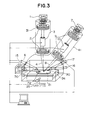
- FIG. 1 and 2 show a whole structure of the apparatus and Fig. 3 shows structures of a focused ion beam optical system, scanning electron microscope optical system and around a sample stage in detail. Shown in this embodiment is a wafer corresponding apparatus in the minute sample processing and observation apparatus of the present invention.
- Fig. 3 shows a schematic bird's eye section of FIG. 1, and there are some differences between the figures, though not essential, in orientations or details of apparatuses for convenience in description.
- Fig. 1 around a center of an apparatus system are appropriately located a focused ion beam optical system 31 and an electron beam optical system 41 above a vacuum sample chamber 60.
- a sample stage 24 on which a wafer 21 to be a sample is placed is located inside the vacuum sample chamber 60.
- Two optical systems 31 and 41 are adjusted in such a manner that their respective central axes intersect at a point on a surface or near the surface of the wafer 21.
- a mechanism for moving the wafer 21 backward and forward, and right and left with high accuracy is provided in the sample stage 24, and is controlled in such a manner that a designated position on the wafer 21 falls immediately below the focused ion beam optical system 31.
- the sample stage 24 has functions of rotational, vertical and slanting movements.
- An exhaust apparatus (not shown) is connected to the vacuum sample chamber 60 and the chamber 60 is controlled so as to have an appropriate pressure.
- the optical systems 31, 41 also individually comprise respective exhaust systems (not shown) and they are maintained at appropriate pressures.
- a wafer introducing device 61 and wafer conveying device 62 are provided within the vacuum sample chamber 60.
- a wafer transferring robot 82 and a cassette introducing device 81 are disposed adjacent to the vacuum sample chamber 60.
- an operation controller 100 for controlling the whole apparatus and a series of processing of sample processing, observation and evaluation.
- the wafer transferring robot 82 pulls out a wafer to be a sample from a designated slot in the cassette, and an orientation adjustment device 83 shown in Fig. 2 adjusts an orientation of the wafer 21 to a predetermined position. Then, the wafer transferring robot 82 places the wafer 21 on a placement stage 63 when a hatch on an upper portion of the wafer introducing device 61 is opened.
- the placement stage 63 When the hatch is closed, a narrow space is formed around the wafer to be a load lock chamber, and after air is exhausted by a vacuum exhaust device (not shown), the placement stage 63 is lowered.
- the wafer conveying device 62 takes up the wafer 21 on the placement stage 63 and places it on the sample stage 24 at a center of the vacuum sample chamber 60.
- the sample stage 24 is provided with means for chucking the wafer 21 according to need in order to correct a warp or prevent vibration of the wafer 21.
- a coordinate value of an observation and analysis position on the wafer 21 is input from the operation controller 100, and the sample stage 24 is moved and stopped when the observation and analysis position of the wafer 21 falls immediately below the focused ion beam optical system 31.
- the focused ion beam optical system 31 comprises an ion source 1, a lens 2 for focusing an ion beam emitted from the ion source 1, an ion beam scanning deflector 3 or the like
- the electron beam optical system 41 comprises an electron gun 7, electron lens 9 for focusing an electron beam 8 emitted from the electron gun 7, an electron beam scanning deflector 10 or the like.
- the apparatus is further provided with a secondary particle detector 6 for detecting a secondary particle from the wafer by applying a focused ion beam (FIB) 4 or the electron beam 8 to the wafer 21, the movable sample stage 24 on which the wafer 21 is placed, a sample stage controller 25 for controlling a position of the sample stage for determining a desired sample position, a manipulator controller 15 for moving a tip of a probe 72 to an extracting position of a minute sample, extracting the minute sample and controlling a position or direction optimum for observation and evaluation of a determined position of the minute sample by applying the focused ion beam 4 (FIB) or electron beam 8 to the minute sample, an X-ray detector 16 for detecting an atomic property X-ray excited at the time of applying the electron beam 8, and a deposition gas supplying device 17.
- FIB focused ion beam
- the sample stage is first lowered and the probe 72 is horizontally (in X and Y directions) moved relative to the sample stage 24 with the tip of the probe 72 separated from the wafer 21, and the tip of the probe 72 is set in a scanning area of the FIB 4.
- the manipulator controller 15 which is a mechanism for operating the probe stores a positional coordinate and then evacuates the probe 72.
- the focused ion beam optical system 31 apples the FIB 4 to the wafer 21 to form a rectangular U-shaped groove across an observation and analysis position p2 as shown in FIG. 4.
- a processing area has a length of about 5 ⁇ m, width of about 1 ⁇ m and depth of about 3 ⁇ m, and is connected to the wafer 21 at its one side surface. Then, the sample stage 24 is inclined, and an inclined surface of a triangular prism is formed by the FIB 4. In this condition, however, the minute sample 22 is connected with the wafer 21 by a support portion S2.
- the inclination of the sample stage 24 is returned, and thereafter, the probe 72 at the tip of the manipulator 70 is brought into contact with an end portion of the minute sample 22. Then, the deposition gas is deposited on a contact point 75 by application of the FIB 4, and the probe 72 is joined to and made integral with the minute sample 22. Further, the support portion S2 is cut by the FIB 4 to cut out the minute sample 22. The minute sample 22 is brought into a condition of being supported by the probe 72, and ready is completed that a surface and an inner section of the minute sample 22 for the purpose of observation and analysis is taken out as an observation and analysis surface p3.
- the manipulator 70 is operated to lift the minute sample 22 up to a level apart from the surface of the wafer 21.
- the observation section p3 of the minute sample 22 may be additionally processed to a desired shape by appropriately adjusting the application angle of the FIB 4 with rotating operation of the manipulator.
- an observation surface has to be a side wall of a hole dug by the FIB, while in the apparatus of this embodiment, the sample can be additionally processed after being lifted, with the observation surface thereof appropriately moved. Therefore, it becomes possible to form a desired section appropriately.
- the minute sample 22 is rotated, and the manipulator 70 is moved in such a manner that the electron beam 8 of the electron beam optical system 41 substantially vertically enters into the observation section p3 to control attitude of the minute sample 22, and then stopped.
- detection efficiency of a secondary electron by the secondary particle detector 6 is increased as much as in the case of observing an outermost surface of the wafer.
- Observation condition of the observation and analysis surface p3 of the minute sample 22 is greatly improved. A reduction in resolution which has been a problem in the conventional method can be avoided.
- the angles of the observation and analysis surfaces p2, p3 can be adjusted to desirable angles, and therefore, it becomes possible to perform more exact observation and analysis.
- the resolution can be improved by transferring a minute sample by movement of the manipulator 70 immediately below the electron beam optical system 41 to reduce a working distance.
- a space in the vacuum container is limited, and it is difficult to bring a large sample close to the electron beam optical system.
- a cut-out minute sample below the electron beam optical system as is in this embodiment, such a problem can be solved.
- the minute sample 22 is observed and analyzed while being placed in the sample chamber of a vacuum atmosphere without taken out of the apparatus, so that observation and analysis of the inner section of the sample to be observed and analyzed can be achieved with high resolution, high accuracy and an optimum angle without contamination or deposition of foreign materials resulting from exposure to the outside atmosphere.
- observation and analysis can be achieved with high throughput of processing more than a few positions per hour. This method also allows observation to be carried out simply by lifting and appropriately positioning the minute sample, which permits facilitating operation and reduction in operation time.
- the section of the semiconductor sample cut by FIB application is moved substantially perpendicularly to the optical axis of the scanning electron microscope to be observed.
- an extremely meritorious effect is exerted in such a case of observing a thin film layer formed in the semiconductor sample.
- wiring formed in the semiconductor wafer has been often formed from copper or the like these days.
- Metal such as copper tends to be diffused in the semiconductor wafer to degrade the property of the semiconductor, so that it is necessary to form a barrier metal around the wiring to prevent diffusion.
- the barrier metal is an extremely thin film with a thickness on the order of 0.01 ⁇ m to 0.02 ⁇ m when the wiring has a thickness of 0.1 ⁇ m to 0.2 ⁇ m, and is formed from metal such as tantalum. In an inspection process of the semi-conductor wafer, whether a barrier metal is formed appropriately or not is an important inspection item.
- the metal which forms the wiring or barrier metal is sometimes corroded or oxidized at its surface when made in contact with the air, thus making it difficult to observe the section.
- the minute sample can be positioned below the optical axis of the FIB without being exposed to the air. Therefore, there is no possibility that a position to be additionally processed is hidden by the oxide film and alignment of processing positions becomes impossible.
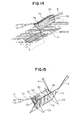
- the minute sample 22 having the observation and analysis surface p3 can be inclined or moved in various ways by the manipulator 70.
- the manipulator 70 it becomes possible, for example, to provide a hole in the observation section p2 and to also confirm three-dimensional fault forming condition in the sample.
- the manipulator 70 and the electron beam optical system 41 are provided opposite to each other with respect to the FIB 4.
- a relative angle between the manipulator 70 and the electron beam optical system 41 is set close to 90° in a surface perpendicular to the application direction of the FIB 4. The reason is that by setting so, it is sufficient that the manipulator 70 simply carries out an operation of lifting the minute sample 22 from the wafer 21, operation of rotating the probe 72 in such a manner that the observation section p2 is perpendicular to the electron beam 8, and other fine adjustment operations.
- the sample stage 24 is provided with a Z-axis moving mechanism for moving the wafer 21 in a Z direction (an optical axis direction of the FIB 4).
- a Z-axis moving mechanism for moving the wafer 21 in a Z direction (an optical axis direction of the FIB 4).
- an electron microscope image of the surface of the wafer 21 slantingly viewed can be obtained.
- a section to be processed or processing arrival position by the FIB 4 is superposed on the electron microscope image to be model displayed, then the section processing condition by the FIB 4 can be easily confirmed.
- animation showing a portion to be a section is displayed on the electron microscope image in the superposed manner based on a processing depth to be set and a dimension in the electron microscope image calculated from magnification.
- the processing depth is calculated in real time based on current and acceleration voltage of the FIB, material of the sample and the like, and an animation showing the present processing depth are displayed in an interposed manner on the electron microscope image, it becomes easy to confirm progress of the processing.
- the electron beam optical system 41 of this embodiment is disposed in a bird's eye position with respect to the wafer 21, and the electron microscope image becomes a bird's eye image. Therefore, by displaying also the above-described animation into three-dimensional display together with the electron microscope image, it is possible to confirm the processing condition more clearly.
- this embodiment has a function of setting a position of the section processing on a scanning ion microscope image (SIM image) formed on the basis of the secondary electron obtained by scanning the wafer 21 with the FIB.
- SIM image scanning ion microscope image
- a portion to be an upside of the observation section p3 is first designated on the SIM image, and the processing depth (a dimension in the depth direction of the observation section p3) is set.
- the forming angle of the inclined portion of the minute sample 22 and the observation and analysis surface p3 are automatically determined, and the subsequent processing is automatically carried out by the settings. It is also possible to provide a sequence where the subsequent processing is automatically carried out by setting the observation and analysis surface p3 (rectangular area) on the SIM image and setting the processing depth.
- the probe 72 is operated so that the observation section p3 is appropriately positioned with respect to the electron beam 8.
- the observation section p3 includes components of not only a rotation around a longitudinal axis of the minute sample 22 but also a rotation around an axis in the application direction of the FIB 4. Imparting a mechanism for removing the rotational components to the manipulator or manipulator controller, and operating the manipulator in timing compliant with the rotation of the probe 72 or timing different from the rotational operation allow the observation section p3 to be accurately positioned in a surface perpendicular to the optical axis of the electron beam 8.
- the same effect can be obtained by disposing the probe 72 to have an angle slightly larger than 90° to the electron beam optical system 41 in the surface perpendicular to the optical axis of the FIB 4.
- the effect is achieved by disposing the probe 72 to a rotational component around the axis in the application direction of the focused ion beam plus 90° with respect to the electron beam optical system 41.
- the rotation axis of the probe 72 is preferably formed in parallel with the surface of the wafer 21 (perpendicular to the optical axis of the FIB 4).
- the rotation axis of the probe 72 so as to be perpendicular to the electron beam optical system 41 so that the sample can be moved below the optical axis of the electron beam 8 by rotation and parallel movement of the probe.
- Specific examples of the structure of the probe will be further described in detail in a description on a subsequent embodiment.
- the minute sample 22 in a suspended condition by the probe 72 is susceptible to vibration, thus in observation and analysis with high magnification and in a locating environment of much vibration, the minute sample 22 may be grounded on a safe position on the wafer 21 or grounded on a minute sample port provided on a space around the wafer on the sample stage to thereby substantially restrain the vibration of the minute sample, permitting superior observation and analysis.
- Fig. 18 shows an example thereof such that earthquake resistance is improved by grounding the cut-out minute sample 22 on the wafer 21. In adopting such a method, it is preferable to make a sequence in advance such that the grounding position of the minute sample matches the optical axis of the electron beam 8.
- the minute sample 22 is processed into pentahedron. This achieves creating of the minute sample especially with reduced waste in processing and in a reduced period of time for separation of the minute sample. It is needless to say that the same effect of the present invention can be obtained by forming the minute sample 22 into tetrahedron (not shown) or a shape close to tetrahedron which can minimize processing time because of the least processing surface.
- the analysis can be used in an inspection of a semiconductor manufacturing process to contribute to improvement of manufacturing yield by early detection of failure and quality control in a short period of time.
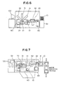
- Fig. 7 is a plan view of Fig. 6, and there are some differences between the figures in orientations or details of apparatuses for convenience in description but they are not essential differences.
- a focused ion beam optical system 31 is vertically disposed and a second focused ion beam optical system 32 is located at an angle of approximately 40° at the upper part of a vacuum sample chamber 60 disposed in the central part of the apparatus system.
- An electron beam optical system 41 is slantingly located at an angle of approximately 45°.
- Three optical systems 31, 32, 41 are adjusted in such a manner that their respective central axes intersect at a point around a surface of a wafer 21.
- a sample stage 24 on which the wafer 21 to be a sample is placed.
- the sample stage 24 in this embodiment has functions of horizontal (X-Y), rotational and vertical movements, but a slanting function is not necessarily required.
- FIG. 4 An FIB 4 is applied from the focused ion beam optical system 31 to the wafer 21 to form a rectangular U-shaped groove across an observation and analysis position p2 as shown in FIG. 4. This is identical to the first embodiment. Then, an inclined surface of a triangular prism is formed by processing with the FIB 4 from another focused ion beam optical system 32. In this condition, however, the minute sample 22 and wafer 21 are connected with each other by a support portion. Then, a minute sample is cut out using the FIB 4 from the focused ion beam optical system 31 similarly to the first embodiment.
- a probe 72 at a tip of a probe holder 71 of a manipulator 70 is brought into contact with an end portion of a minute sample 22, and then deposition gas is deposited on a contact point 75 by application of the FIB 4, where the probe 72 is joined to and made integral with the minute sample 22, and the support portion is cut by the FIB 4 to cut out the minute sample 22.
- Subsequent steps of observation and analysis of the minute sample 22 are identical to the first embodiment.
- slanting of the sample stage can be eliminated especially by using two focused ion beam optical systems. Omitting the slanting mechanism of the sample stage can improve positioning accuracy of the sample stage more than a few to ten times.
- various wafer inspection and evaluation apparatus carry out a foreign material inspection and defect inspection, that a property and coordinate data of a wrong portion on the wafer are recorded, and that subsequent apparatus for a further detail inspection receives the coordinate data to determine a designated coordinate position and to carry out observation and analysis.
- High positioning accuracy permits automation of determining the observation position of the wafer 21 and simplification of its algorithm. This can substantially reduce required time, which permits obtaining high throughput. Further, the sample stage having no slanting mechanism is compact and lightweight and can easily obtain high rigidity to increase reliability, thus permitting superior observation and analysis and miniaturization or a reduction in cost of the apparatus.
- Fig. 9 is a plan view of Fig. 8, and there are some differences between the figures in orientations or details of apparatuses for convenience in description but they are not essential difference.
- a focused ion beam optical system 33 is slantingly located at an angle of approximately 45° at an upper portion of a vacuum sample chamber 60 disposed at the central part of the apparatus system.
- An electron beam optical system 42 is also slantingly located at an angle of approximately 45°.
- Two optical systems 33, 42 are adjusted in such a manner that their respective central axes intersect at a point around a surface of a wafer 21.
- a sample stage 24 inside the vacuum sample chamber 60 is located a sample stage 24.
- the sample stage 24 has no slanting function.
- the sample stage is first lowered to move a probe 72 horizontally (in X and Y directions) relative to the sample stage 24 with the tip of the probe 72 separated from the wafer 21, and the tip of the probe 72 is set in a scanning area of the FIB 4.
- the manipulator controller 15 stores a positional coordinate and then evacuates the probe 72.
- the sample stage is oriented in such a manner that an intersection line of a vertical plane containing an optical axis of a focused ion beam optical system 33 and a top surface of the wafer is superposed on an observation section of a sample to be formed.
- an FIB 4 is applied to the wafer 21 for scanning to form a vertical section C1 having a length and depth required for the observation.
- an inclined cut section C2 which intersects a formed section is formed.
- the sample stage is rotated around a horizontal axis up to a position where an inclination angle of an inclined surface is obtained to determine the orientation.
- an inclined groove is formed by the FIB 4 in parallel with a vertical cut line.
- a processing area has a length of about 5 ⁇ m, width of about 1 ⁇ m and depth of about 3 ⁇ m, and is connected to the wafer 21 in a cantilevered condition of a length of about 5 ⁇ m. Then, the probe 72 at the tip of a manipulator 70 is brought into contact with an end portion of a minute sample 22, and then deposition gas is deposited on a contact point 75 by application of the FIB 4, where the probe 72 is joined to and made integral with the minute sample 22. Then, the other end C4 supporting the minute sample is cut by the FIB 4 to cut out the minute sample 22.
- the minute sample 22 is brought into a condition of being supported by the probe 72, and ready to be taken out with a surface and an inner section for the purpose of observation and analysis as an observation and analysis surface p3 is completed. Processing thereafter is substantially identical to the first embodiment except that an orientation of the sample stage 24 is also required to be appropriately adjusted when setting the optimum orientation of the minute sample for processing and observation by the focused ion beam optical system or observation by electron beam optical system, and thus description thereof will be omitted.
- This embodiment has a feature that one focused ion beam optical system is inclined with respect to the sample stage to thereby cut out and extract the minute sample from the wafer without imparting a slanting function to the sample stage.
- a large number of devices are required to be mounted around the optical system, causing lack of spaces, and a large total mass of the devices makes difficult design of a mounting substrate including ensuring rigidity. Maintenance thereof is also a matter of concern.
- This embodiment eliminates the need for a slanting mechanism of the sample stage, and requires only one focused ion beam optical system, which can provide a simple, compact and lightweight structure and reduced cost.
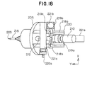
- a second sample stage 18 and second sample stage controller 19 for controlling an angle, a height and the like of the second sample stage are added to a basic structure of the minute sample processing and observation apparatus shown in Fig. 3.
- the process from applying an ion beam from the focused ion beam optical system 31 to a wafer to extracting a minute sample from the wafer is identical to the first embodiment.
- the extracted minute sample is fixed to the second sample stage for observation and analysis instead of observation and analysis in the supported condition by the manipulator.
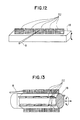
- Fig. 11 shows a condition of the minute sample 22 fixed to the second sample stage 18.
- a member with a flattened surface is used for a minute sample fixed portion of the second sample stage 18 in this embodiment, but flatness does not matter.
- a bottom surface of the minute sample is brought into contact with the second sample stage 18, and deposition gas is deposited on a contact point between the second sample stage 18 and minute sample 22 with the FIB 4 to fix the minute sample 22 to the second sample stage 18 with an assist deposition film 76.
- an application angle of the FIB 4 may be appropriately set in parallel to the observation section of the minute sample by operating the second sample stage to create a desired observation section by applying the FIB 4.
- a plurality of minute samples can be collectively handled.
- section observation and elementary analysis of the plurality of samples can be carried out with the wafer 21 fixed to the sample stage 24, and distribution of a section structure throughout the wafer 21 can be efficiently examined.
- Fig. 12 when fixing the plurality of minute samples in a line to the second sample stage 18 and carrying out observation and analysis in a condition where both of a stopping orientation of the sample stage 24 and an angle of the second sample stage 18 are adjusted so as to locate the minute sample 22 at an appropriate angle to the electron beam 8, the plurality of minute samples can be observed and analyzed successively or repeatedly with compared to one another, thereby permitting detailed and efficient examinations of the section structure and elementary distribution throughout the wafer 21.
- the second sample stage 18 shown in Fig. 13 is a rotatable column sample stage such that a minute sample group can be arranged on its outer peripheral surface, and a larger number of minute samples can be handled at a time than in the case of Fig. 12.
- the minute samples 22 By detaching the minute samples 22 to be recovered in a designated position in a sample recovery tray and providing identification means for the minute samples, the minute samples 22 can be taken out again for observation and analysis when a detailed evaluation is required afterward.
- secondary electron detecting efficiency can be obtained as high as in the case of observing the wafer surface, an angle for observation and analysis can be adjusted to a desirable angle including vertical observation, observation can be carried out with placed in a sample chamber of a vacuum atmosphere, and the like, therefore, observation condition of the minute sample 22 is greatly improved to permit avoiding a reduction in resolution which has been a conventional problem and carrying out optimum, exact observation and analysis promptly with high speed and high efficiency. As a result, superior observation and analysis can be carried out with high throughput.
- vibration isolating mechanism of the sample stage which holds the introduced sample and vibration isolating mechanism of the second sample stage to which the minute sample is fixed can be shared.
- Fig. 16 is an explanatory view of the embodiment.
- a sample chamber vacuum container
- An optical system 226 comprising an ion source 225, beam limiting aperture 228, focusing lens 229, deflector 230 and objective lens 231 are basically the same as in Fig. 3, and an FIB 227 is adjusted which is applied along an optical axis 224. Further, the apparatus shown in Fig. 16 is provided with a sample holder 233a for holding a wafer 217 and a stage 234 for moving the sample holder in X-Y directions.
- the apparatus is further provided with a secondary electron detector 237 for detecting a secondary electron discharged from the sample resulting from application of the FIB 227, a deposition gas source 238 for blasting a deposition gas concurrently with application of the ion beam and a vacuum container 206 for maintaining high vacuum in the sample chamber.
- An output of the secondary electron detector 237 is amplified by an amplifier (not shown) and then stored in an image memory (not shown) and displayed on an image display apparatus 238.
- a central processing unit 240 controls various components of the apparatus shown in Fig. 16 via an FIB controller 236, a probe position controller 223, and stage position controller 235.
- An air lock chamber 202 provided in the probe moving mechanism 201 is coupled to a base flange 205 via bellows 204 absorbing a moving amount of a probe 203.
- the base flange 205 is fixed to a vacuum container 206 with a vacuum seal 207 interposed therebetween.
- a closable air lock valve 208 is disposed at an end of the air lock chamber 202, and opened/closed by rotating a cylindrical air rock valve opening/closing mechanism 209. Shown in Fig.
- FIG. 17 is a condition where the air lock valve 208 is opened and a probe holder 210 is introduced into the vacuum container 206 in such a manner that its central axis is inclined to a surface of the wafer 217.
- An air rock chamber outer cylinder 211 in which the air lock valve 208 and air rock valve opening/closing mechanism 209 are accommodated has a concentrical hollow double structure, and one end of the hollow portion communicates with the air lock chamber 202 and the other end communicates with an exhaust pipe 212.
- the above structure eliminates the need for compact bellows for the air lock chamber 202 which has been conventionally required, permitting simplification, miniaturization and reduction in cost of the probe moving mechanism 201.
- a current introduction terminal 214 having a sealing function is disposed on a fixed side flange 213 of the bellows 204.
- a vacuum side of the current introduction terminal 214 is connected via a lead wire 216 to a probe holder 249 which holds the probe 203 and is formed from an insulating material with conduction at portions in contact with the probe 203 and probe holder stopper 215, power can be supplied from an air side to the probe 203.
- a Y-axis stage 219a is fixed where a Y-axis linear guide 218a is fixed in parallel with the surface of the wafer 217 as shown, and coupled to a Y-axis base 220 via the Y-axis linear guide 218a as shown in Fig. 18.
- Linear driving of a Y-axis is carried out using a Y-axis linear actuator 221a held by the Y-axis base 220.
- An output shaft of the Y-axis linear actuator 221a is coupled to a Y-axis stage 219a via a Y-axis lever 222a.
- the Y-axis base 220 is coupled to a Z-axis stage 219b.
- the Z-axis stage 219b is coupled to an X-axis stage 219c via a Z-axis linear guide 218b disposed perpendicularly to the surface of the wafer 217 having a phase 90° different from the Y-axis linear guide 218a as shown.
- the linear driving of the Z-axis stage 219b is carried out using a Z-axis linear actuator 221b held by the X-axis stage 219c.
- An output shaft of the Z-axis linear actuator 221b is coupled to the Z-axis stage 219b via a Z-axis lever 222b.
- the X-axis stage 219c is coupled to the base flange 205 via an X-axis linear guide 218c disposed in parallel with the surface of the wafer 217 having a phase 90° different from the Y-axis linear guide 218a as shown.
- the linear driving of the X-axis stage 219c is carried out using an X-axis linear actuator 221c held by the base flange 205.
- An output shaft of the X-axis linear actuator 221c is coupled to the X-axis stage 219c via an X-axis lever 222c.
- the probe moving mechanism 201 of this embodiment has a width of 172 mm in the X-axis direction and a height of 165 mm in the Z-axis direction which are substantially identical to the width and height of the used linear actuator.
- the probe holder 210 is inserted in front of the air lock valve 208.
- the air lock chamber 202 is kept to be sealed by the vacuum seal 207 arranged in an outer cylinder of the probe holder 210.
- air in the air lock chamber 202 is exhausted to be a vacuum from the exhaust pipe 212 through a hollow portion of the air lock chamber outer cylinder 211.
- the air lock valve 208 is opened using the air lock valve opening/closing mechanism 209, and the probe holder 210 is introduced into the vacuum container 206.
- the above described operations allow the probe 203 to be introduced into the vacuum container 206 without the vacuum container 206 being exposed to the air.
- Extracting the probe holder 210 from the vacuum container 206 can be carried out by the procedure in the reverse order of the insertion. That is, the probe holder 210 is once extracted in front of the air lock valve 208, then the air lock valve 208 is closed using the air lock valve opening/closing mechanism 209. Confirming the closure, the air in the air lock chamber 202 is leaked from the exhaust pipe 212. After confirming an atmospheric pressure, the probe holder 210 is taken out of the probe moving mechanism 201. Adopting the above structure allows replacement of the probe 203 which is a consumable supply to be carried out without the vacuum container 206 being exposed to the air.
- the probe holder 210 by structuring the probe holder 210 in such a manner that a substantially central axis of the probe holder 210 enters slantingly to the wafer 217 (in this embodiment, enters at an angle of 30°), the probe holder 210 can reach near the optical axis 224 of the charged particle beam optical system with a minimum length, which permits providing the probe holder 210 with high rigidity and remarkably facilitating handling of the few ⁇ m sample piece 232 and operations of making the tip of the probe into contact with a predetermined position on an electron element having a submicron wiring.
- Machine parts such as the bellows 204 for absorbing the mounting amount of the probe 203 are not positioned lower than the surface of the wafer 217, so that the probe moving mechanism 201 has no influence on the size of the vacuum container 206, and the vacuum container 206 may be a minimum size determined within a movement range of the wafer 217.
- Minimizing the vacuum container 206 which determines the size of the apparatus can provide a sample creating apparatus for samples with large diameters mounted with a probe moving mechanism, which permits reduction in occupying area, weight and cost and also miniaturization of exhaust means.
- the entering angle of the probe holder 210 is 30°, but not limited to this. The same effect can be obtained by inserting the probe holder 210 slantingly to the vacuum container 206 in such a manner that the probe 203 is within a range of being displayed by the image display apparatus 238.
- the probe moving mechanism 201 By arranging the probe moving mechanism 201 in a position where a distance to the intersection point of the center of the base flange 205 which couples the probe moving mechanism 201 to the vacuum container 206 and a vertical line of the optical axis 224 is below 1/2 of the horizontal movement range of the sample stage 234, below 150 mm in this embodiment, the probe holder 210 can be introduced into the vacuum container 206 with a minimum length at a desired angle, and freedom of a layout of the apparatus can be increased while permitting the vacuum container 206 to be miniaturized.
- the probe moving mechanism 201 can eliminate projections, thus imposing no limitation in the layout to other measurement instruments arranged in the vacuum container 206, preventing problems of unexpected interference or the like and achieving miniaturization of the apparatus.
- the ion beam 227 emitted from the ion source 225 is focused on a predetermined position on the stage 234 by passing through the optical system 226.
- the focused ion beam, that is, FIB 227 is spattered in the form of scanning the surface of the wafer 217 to carry out fine processing of the sample piece (not shown).
- the stage position controller 235 determines a position to be FIB processed and extracted.
- the probe 203 mounted on the probe moving mechanism 201 is moved to an extracting position on the wafer 217 independently of the stage 234 by the probe position controller 223. Operations of movement and processing are carried out while observing by scanning with the FIB around the extracting position of the wafer 217 by the FIB controller 236, detecting the secondary electron from the wafer 217 by the secondary electron detector 237, and displaying the obtained secondary particle image on the image display apparatus 238.
- the FIB processing is carried out while changing the attitude of the wafer 217 to cut out the sample piece in the form of a wedge, and deposition gas is supplied to the contact portion of the sample piece where the probe 203 is made into contact with using the deposition gas source 239, and an ion beam assist deposition film is formed to thereby attach the probe 203 to the sample piece.
- the prove 203 is then raised from the wafer 217 by the probe position controller 223, and moved to a position of the sample holder 233b on the stage 234.
- the probe 203 is lowered, contact between the wedge portion of the sample piece attached to the probe 203 and the surface of the sample holder 233b is confirmed, and a side surface of the sample piece is attached to the sample holder 233a by the ion beam assist deposition film.
- the tip of the probe 203 is cut from the sample piece 232 by the FIB and moved to a next sample extracting position by the probe position controller 223.
- the above processes make it possible to extract the sample piece 232 at a desired position from the wafer 217 and move it to the sample holder 233b.
- the above operations are collectively controlled by a central processing unit 240.
- This embodiment adopts the ion beam assist deposition film as the attaching means between the probe 203 and the sample piece 232, but there is no problem in electrostatic attaching means using an attaching force by static electricity, and the same effect can be obtained as this embodiment in that case.
- attachment by the assist deposition film is desirable for attaching the probe to the accurate position.
- the probe moving mechanism is structured to be slantingly inserted, thereby permitting miniaturization of the sample chamber (vacuum container) in comparison with a probe moving mechanism which is inserted horizontally of the wafer surface disclosed in JP-A-11-56602 specification.
- the machine parts such as bellows for absorbing the moving amount of the probe are inevitably positioned lower than the surface of the wafer, therefore the machine parts have to be placed in a position which has no interference with the stage on which the wafer is placed, that is, out of the movement range of the stage.
- This inevitably causes upsizing of the vacuum container, but the present invention can achieve miniaturization of the vacuum container, and the resultant reduction in an occupying area and cost and miniaturization of a vacuum exhaust pump.
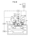
- Fig. 19 is a sectional view of a sample creating apparatus of a sixth embodiment using a slantingly entering sample stage fine moving device 241. Described in the former embodiment has been the example of providing an electron beam barrel in the same sample chamber as the ion beam barrel and observing the sample cut out by the electron beam barrel. However, described in this embodiment is an example of transferring a cut-out sample to other analyzer using a side entry type sample stage and observation is carried out.
- the side entry type sample stage means a stage to be inserted from the side of a charged particle beam barrel or the sample chamber, and details thereof will be described below.
- Fig. 20 is an enlarged view of portions around the probe 203 in Fig. 19, and Fig. 21A is a vertical sectional view and Fig. 21B is a horizontal sectional view of a side entry type sample stage 242 used in Fig. 19.
- a sample locating portion 243 to which a sample piece 232 is attached is held by a sample holder 233a.
- a projection 245 is provided on an end surface of a driving shaft 244 side of the sample holder 233a.
- the shape of the projection 245 does not matter.
- Sample creation using the sample creating apparatus takes the following steps.
- the operations of introducing and extracting the side entry type sample stage 242 into and from the vacuum container 206 are the same as the operations of the probe holder 210 in the above described probe moving mechanism 201.
- the same processes as the fifth embodiment are adopted.
- the side entry type sample stage 242 is inserted into the vacuum container 206 without being exposed to the air.
- the size of the vacuum container 206 can be minimized, and the side entry type sample stage 242 can reach near an intersection point of the optical axis 224 of the FIB 227 and the wafer 217 with a minimum length.
- the side entry type sample stage 242 slantingly enters at an angle of 30° to the surface of the wafer 217, but not limited to 30°.
- the same effect can be obtained by slantingly inserting the side entry type sample stage 242 into the vacuum container 206 in such a manner that the sample holder 233a exists within a range of being displayed by an image display apparatus 238.
- the sample stage fine moving mechanism 241 has no influence on the size of the vacuum container 206 and the vacuum container 206 can be a minimum size which is determined by a movement range of the wafer 217.
- the side entry type sample stage 242 can be introduced with a minimum length at a desired angle, and freedom of a layout of the apparatus can be increased while permitting the vacuum container 206 to be miniaturize.
- the knob 247 is turned to rotate the sample locating portion 243 held by the sample holder 233a at an angle in parallel with the wafer 217 as shown in Fig. 20, that is 30° in this embodiment. Then, the probe 203 holding the sample piece 232 is driven by the probe moving mechanism 201 and the probe position controller 223 shown in Fig. 19, and the minute sample piece 232 is attached to the sample holder 233a by forming a deposition film.
- the sample holder 233a After attachment, the sample holder 233a is again rotated to the position in parallel with the axis of the side entry type sample stage 242, and the side entry type sample stage 242 is then extracted from the vacuum container 206 by the above described means, and for example, mounted to a TEM apparatus (not shown) to thereby carry out TEM observation.
- the rotation of the sample holder 233a is used for fine rotational adjustment of the sample piece 232 in the TEM observation to permit more reliable analysis.
- the FIB apparatus can be realized which has the vacuum container 206 with the size restricted to the same size as in the fifth embodiment, the probe moving mechanism 201 which can extract the sample piece 232 at a desired position on the wafer 217 and the side entry type sample stage 242 which can be mounted to various analyzers.
- this FIB apparatus it becomes possible to transfer the sample piece 232 at a desired position of the wafer 217 with a large diameter to the sample holder 233a in the vacuum container 206, and further, by taking out the side entry type sample stage 242 on which the sample holder 233a is placed without being exposed to the air, prompt mounting on various analyzers and evaluation become possible.
- a sample stage fine moving device with the same manner as the probe moving mechanism 201, improvements of productivity, maintainability, and operability of an apparatus can be realized.
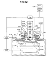
- Fig. 22 is a sectional view of a sample creating apparatus of still another embodiment.
- the embodiment differs from the sixth embodiment in that it uses a probe moving mechanism 201 having a probe holder 210 in which freedom of rotation around a Y-axis shown by the coordinate system shown in Fig. 16 is added to a probe 203 shown in Fig. 23, and a sample stage fine moving mechanism in which freedom of rotation around a central axis of a side entry type sample stage 242 is added to a sample holder 233a shown in Fig. 24.
- Fig. 23A shows the probe 203 in a projected condition
- Fig. 23B shows the probe 203 accommodated in an outer cylinder 248.
- the probe 203 is fixed to a probe holder 249 through a leaf spring 252, and the probe holder 249 is held in an inner cylinder 251 which linearly moves through a bearing 250.
- the inner cylinder 251 is inserted into an outer cylinder 248 with freedom in a rotating direction being limited, and pressed against a driving shaft 253 via a bearing 254.
- An end of the probe holder 249 is connected to a helical compression spring 259, and the other end of the helical compression spring 259 is coupled to the driving shaft 253.
- a rotation center of the bearing 250 is inclined to a center line of the probe holder 210 at an insertion angle of the probe holder 210. This allows the probe 203 to be rotationally moved in parallel with the surface of the wafer 217 in the vacuum container 206. If such a probe is applied to the apparatus described in the first embodiment, observation by a scanning electron microscope capable of non destructive observation with high resolution becomes compatible with application substantially in a vertical direction to the sample section. As is the apparatus of the present invention, in an apparatus handling large samples, a probe and a moving mechanism of the probe must be disposed above the samples. However, the probe and the probe moving mechanism disclosed in Fig. 23 permit rotation of a cut out minute sample around a rotation axis parallel to a sample surface.
- the driving shaft 253 is inserted into the outer cylinder 248 with a bearing 255 for rotation and linear moving and a vacuum seal (not shown) interposed. An end of the driving shaft 253 projects from the outer cylinder 248.
- a gear 256b is fixed to the projected portion of the driving shaft 253, and a minute feeding mechanism 257 which is an actuator of linear movement is pressed against an end surface of the driving shaft 253.
- Another gear 256a in mesh with the gear 256b is arranged in parallel with the driving shaft 253, and a knob 247 for rotary movement is fixed to the gear 256a. It is needless to say that the gears 256a, 256b are held via rotatable members, though not shown.
- the above is the basic structure of the probe holder 210 having two degrees of freedom of rotation and accommodation of the probe 203.
- the driving shaft 253 is linearly moved using the minute feeding mechanism 257.
- the linear movement of the driving shaft 253 is transferred to the outer cylinder 248, thus the probe 203 held by the probe holder 210 is linearly moved without rotation.
- the probe 203 is rotationally moved by turning the knob 247, rotationally moving the driving shaft 253 via the gears 256a, 256b. Since freedom of rotation of the inner cylinder 251 is limited, the rotary movement of the driving shaft 253 does not cause rotary movement of the inner cylinder 251. An elastic deformation by the helical compression spring 259 changes a direction of the rotary movement, but the rotary power is transferred to the probe holder 249, and the probe holder 249 held via the inner cylinder 251 and bearing 250 for rotation is rotationally moved. As described above, by simple operations of linear and rotary movements of a single driving shaft 253, the probe 203 can move linearly and rotationally.
- a gear 261a is disposed on a grip 260 of a side entry type sample stage 242, and a gear 261b in mesh with the gear 261a and a driving source 262 for rotatably driving the gear 261b are disposed on a Y-axis stage 219a.
- the side entry type sample stage 242 can be inclined at a desired angle by rotationally moving the sample holder 233a portion together with the whole side entry type sample stage 242.
- the gear 261a coupled to the side entry type sample stage 242 can be coupled to the gear 261b coupled to the driving source 262 using no mechanical parts such as screws with no bars in inserting and extracting the side entry type sample stage 242.
- Fig. 25 shows operations of processing the sample piece 232 by the sample creating apparatus of Fig. 22. Sample creating by the sample creating apparatus of this embodiment will be described with reference to this figure. The same steps as the fifth embodiment are adopted before the step (a) for extracting the sample piece 232 from the wafer 217.
- the sample piece 232 is transferred on a sample locating portion 243 rotationally moved in parallel with the surface of the wafer 217 without rotating the probe 203.
- the sample piece 232 is extracted from the wafer 217 and then the probe 203 is rotated at an angle of 90°, and the X-, Y- and Z-axes are driven if necessary, and the sample piece 232 is attached by the ion beam assist deposition film to the sample locating portion 243 which has been rotationally moved in parallel with the surface of the wafer 217 (Fig. 25 (b)).
- the probe 203 is linearly moved using the minute feeding mechanism 257 so as to be accommodated in the outer cylinder 248. Then, the knob 247 is turned to reset the inclined sample holder 233a holding the sample locating portion 243 (Fig. 25 (c)). Then, the driving source 262 is driven, and the sample holder 233a is rotationally moved in such a manner that the sample locating portion 243 is opposed to the FIB 227, and the sample piece 232 is forming worked by the FIB 227 (Fig. 25 (d)).
- sample creating apparatus analysis of the outermost surface layer and in the depth direction of the wafer 217 is possible, and further, a wide range of sample analyses is possible because of having the same structure as the side entry type sample stage 242 capable of being mounted to various analyzers, thereby greatly enlarging a range of utilization as the sample creating apparatus.
- the sample surface can be easily analyzed or observed by configuring the apparatus so as to be mounted to any one of the focused ion beam apparatus, transmission electron microscope, scanning electron microscope, scanning probe microscope, Auger electron spectroscopic analyzer, electron probe X-ray microanalyzer, electronic energy deficiency analyzer, secondary ion mass spectroscope, secondary neutron ionization mass spectroscope, X-ray photoelectron spectroscopic analyzer, or electrical measuring apparatus using a probe.
- the ion beam barrel and electron beam barrel are relatively inclined to the sample placing surface of the sample stage.
- the sample piece is separated from the sample placed on the sample stage by the ion beam, and is joined in an deposited manner by the ion beam and gas to a needle member mounted to the tip of the probe and is extracted.
- the extracted sample piece is moved below the electron beam rotated such that the electron beam can be applied to a predetermined portion.
- the secondary electron from the sample may be detected by the detector to obtain a scanning electron microscope image.
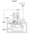
- Fig. 26 is a sectional view of an embodiment where a probe moving mechanism 201 according to the present invention is applied to a failure inspection apparatus.
- an electron beam 266 emitted form an electron gun 265 passes through an electron beam optical system 267 and is focused on a surface of a wafer 217 placed on a stage 234.
- the stage 234 is controlled by a stage position controller 235 to determine position of an element to be evaluated on the wafer 217.
- only two probe moving mechanisms 201 are shown, but another two probe moving mechanisms 201 are arranged opposite in the direction perpendicular to the sheet surface, thus the failure inspection apparatus is provided with four probe moving mechanisms 201.
- a probe 203 arranged in each of four probe moving mechanisms 201 is moved to the position of the evaluation element on the wafer 217 by the probe position controller 223 capable of being driven independently of the stage 234. Movement is carried out with confirming in such a manner that an electron beam controller 271 scans around the evaluation element on the wafer 217 with an electron beam 266, and that a secondary electron from the wafer 217 is detected by a secondary electron detector 237 to display an image of the element portion on an image display apparatus 238.
- a power supply 269 is connected to each probe 203 so that voltage can be applied to a minute portion of the wafer 217 with which applied to a minute portion of the wafer 217 with which the probe 203 comes into contact.
- an amperemeter 270 is also connected to each probe 203 so that a current flowing in each probe 203 can be measured.
- an evaluation method a case in a MOS device formed on the wafer 217 is described. First, three probes 203 are brought into contact with a source electrode, a gate electrode and a drain electrode, respectively.
- the source electrode is grounded using the probe 203, and while exciting voltage of the gate electrode as a parameter by the probe 203, a relationship between a drain voltage and a drain current flowing between the source and a drain by the probe 203. This provides an output property of the MOS. These operations are collectively controlled by the central processing unit 240.
- the probe moving mechanism 201 of the slant entering type shown in Figs. 17 and 18 is used, so that an inspection of the wafer 217 with a large diameter can be achieved with a compact apparatus. Further, since the structure of probe moving mechanism 201 is one that the replacement or the like of the probe 203 can be easily carried out, and therefore, an operating rate of the apparatus can be improved.
- Fig. 27 is a sectional view when a probe moving mechanism 201 of the present invention is figure, an FIB 227 emitted from the ion source 225 is focused on a desired position on the stage 234 by passing through an optical system 226.
- the focused ion beam, that is, FIB 227 is spattered in the form of scanning the surface of the wafer 217 to carry out fine processing.
- the stage position controller 235 determines an observation position on the wafer 217.
- the probe 203 mounted on the probe moving mechanism 201 is moved to the observation position on the wafer 217 by the probe position controller 223 which can drive independently of the stage 234.
- Movement and processing are carried out while observing in such a manner that the FIB controller 236 scans around the observation position on the wafer 217 with the FIB, that a secondary electron from the wafer 217 is detected by a secondary electron detector 237, and that an obtained secondary particle image is displayed on an image display apparatus 238.
- a power supply 269 is connected to the probe 203 so that voltage can be applied to a minute portion of the wafer 217 with which the probe 203 is brought into contact.
- a groove is provided around a circuit by the FIB so as to electrically isolate the circuit to be observed from other circuits.
- the voltage applied probe 203 is brought into contact with an end of the circuit, and a position is observed which is considered to be connected to the circuit in design.
- the probe moving mechanism 201 of the slant entering type shown in Figs. 17 and 18 is used, so that an inspection of the wafer 217 with a large diameter can be achieved with a compact apparatus. Further, since the structure of probe moving mechanism 201 is one that the replacement or the like of the probe 203 can be easily carried out, and therefore, an operating rate of the apparatus can be improved.
- a sample creating apparatus using a projection ion beam which is structure by replacing a deflector 230 and an objective lens 231 with a mask plate and a projection lens or a sample observing apparatus using a laser beam which is structured by replacing an ion source 225 with a laser source.
Landscapes
- Engineering & Computer Science (AREA)
- Analytical Chemistry (AREA)
- Chemical & Material Sciences (AREA)
- Physics & Mathematics (AREA)
- Signal Processing (AREA)
- Computer Networks & Wireless Communication (AREA)
- General Health & Medical Sciences (AREA)
- Life Sciences & Earth Sciences (AREA)
- Health & Medical Sciences (AREA)
- Biochemistry (AREA)
- Computer Security & Cryptography (AREA)
- General Physics & Mathematics (AREA)
- Immunology (AREA)
- Pathology (AREA)
- Plasma & Fusion (AREA)
- Sampling And Sample Adjustment (AREA)
- Analysing Materials By The Use Of Radiation (AREA)
- Testing Or Measuring Of Semiconductors Or The Like (AREA)
Priority Applications (1)
| Application Number | Priority Date | Filing Date | Title |
|---|---|---|---|
| EP08020171A EP2043131B1 (de) | 2000-11-02 | 2001-09-19 | Verfahren zur Herstellung von winzigen Proben |
Applications Claiming Priority (4)
| Application Number | Priority Date | Filing Date | Title |
|---|---|---|---|
| JP2000340387A JP4178741B2 (ja) | 2000-11-02 | 2000-11-02 | 荷電粒子線装置および試料作製装置 |
| JP2000340387 | 2000-11-02 | ||
| JP2000344226 | 2000-11-07 | ||
| JP2000344226A JP3736333B2 (ja) | 2000-11-02 | 2000-11-07 | 微小試料加工観察装置 |
Related Child Applications (2)
| Application Number | Title | Priority Date | Filing Date |
|---|---|---|---|
| EP08020171A Division EP2043131B1 (de) | 2000-11-02 | 2001-09-19 | Verfahren zur Herstellung von winzigen Proben |
| EP08020171.8 Division-Into | 2008-11-19 |
Publications (3)
| Publication Number | Publication Date |
|---|---|
| EP1204133A2 true EP1204133A2 (de) | 2002-05-08 |
| EP1204133A3 EP1204133A3 (de) | 2007-11-14 |
| EP1204133B1 EP1204133B1 (de) | 2011-03-30 |
Family
ID=26603585
Family Applications (2)
| Application Number | Title | Priority Date | Filing Date |
|---|---|---|---|
| EP01121770A Expired - Lifetime EP1204133B1 (de) | 2000-11-02 | 2001-09-19 | Vorrichtung zur Behandlung einer Mikroprobe |
| EP08020171A Expired - Lifetime EP2043131B1 (de) | 2000-11-02 | 2001-09-19 | Verfahren zur Herstellung von winzigen Proben |
Family Applications After (1)
| Application Number | Title | Priority Date | Filing Date |
|---|---|---|---|
| EP08020171A Expired - Lifetime EP2043131B1 (de) | 2000-11-02 | 2001-09-19 | Verfahren zur Herstellung von winzigen Proben |
Country Status (4)
| Country | Link |
|---|---|
| US (10) | US6781125B2 (de) |
| EP (2) | EP1204133B1 (de) |
| JP (2) | JP4178741B2 (de) |
| DE (1) | DE60144319D1 (de) |
Cited By (11)
| Publication number | Priority date | Publication date | Assignee | Title |
|---|---|---|---|---|
| EP1870691A2 (de) * | 2006-06-23 | 2007-12-26 | FEI Company | Herstellung einer planaren Sichtprobe |
| WO2009050127A2 (de) * | 2007-10-10 | 2009-04-23 | Suss Microtec Test Systems Gmbh | Sondenhaltervorrichtung |
| EP2095134A2 (de) * | 2006-10-20 | 2009-09-02 | FEI Company | Verfahren und vorrichtung zur probenextraktion und -handhabung |
| CN100592065C (zh) * | 2006-11-03 | 2010-02-24 | 中国科学院金属研究所 | 一种用离子束加工样品界面实现背散射表征的方法 |
| US8134124B2 (en) | 2006-10-20 | 2012-03-13 | Fei Company | Method for creating S/tem sample and sample structure |
| CN104049097A (zh) * | 2013-03-15 | 2014-09-17 | Fei公司 | 用于高生产能力样品制备的到纳米操纵器的多样品附接 |
| US8969835B2 (en) | 2012-01-23 | 2015-03-03 | Carl Zeiss Microscopy Gmbh | Particle beam system including a supply of process gas to a processing location |
| CN105047512A (zh) * | 2015-05-29 | 2015-11-11 | 光驰科技(上海)有限公司 | 具备多层载物能力的离子束刻蚀系统及其刻蚀方法 |
| EP2748579B1 (de) * | 2011-08-25 | 2016-01-06 | Fraunhofer Gesellschaft zur Förderung der angewandten Forschung E.V. | Verfahren zur präparation einer probe für die mikrostrukturdiagnostik |
| EP2991096A1 (de) * | 2014-08-29 | 2016-03-02 | Hitachi High-Tech Science Corporation | System mit geladenem teilchenstrahl |
| US10677697B2 (en) | 2014-06-30 | 2020-06-09 | Hitachi High-Tech Science Corporation | Automatic sample preparation apparatus |
Families Citing this family (178)
| Publication number | Priority date | Publication date | Assignee | Title |
|---|---|---|---|---|
| JP4178741B2 (ja) | 2000-11-02 | 2008-11-12 | 株式会社日立製作所 | 荷電粒子線装置および試料作製装置 |
| DE60144508D1 (de) * | 2000-11-06 | 2011-06-09 | Hitachi Ltd | Verfahren zur Herstellung von Proben |
| US20040257561A1 (en) * | 2000-11-24 | 2004-12-23 | Takao Nakagawa | Apparatus and method for sampling |
| JP4200665B2 (ja) * | 2001-05-08 | 2008-12-24 | 株式会社日立製作所 | 加工装置 |
| JP3820964B2 (ja) * | 2001-11-13 | 2006-09-13 | 株式会社日立製作所 | 電子線を用いた試料観察装置および方法 |
| JP2003156418A (ja) * | 2001-11-26 | 2003-05-30 | Mitsubishi Electric Corp | 分析用試料の作製方法および分析方法並びにその分析用試料 |
| JP4302933B2 (ja) * | 2002-04-22 | 2009-07-29 | 株式会社日立ハイテクノロジーズ | イオンビームによる穴埋め方法及びイオンビーム装置 |
| DE10233002B4 (de) * | 2002-07-19 | 2006-05-04 | Leo Elektronenmikroskopie Gmbh | Objektivlinse für ein Elektronenmikroskopiesystem und Elektronenmikroskopiesystem |
| JP2004093353A (ja) * | 2002-08-30 | 2004-03-25 | Seiko Instruments Inc | 試料作製装置 |
| US6877894B2 (en) * | 2002-09-24 | 2005-04-12 | Siemens Westinghouse Power Corporation | Self-aligning apparatus for acoustic thermography |
| US7150811B2 (en) * | 2002-11-26 | 2006-12-19 | Pei Company | Ion beam for target recovery |
| JP4088533B2 (ja) * | 2003-01-08 | 2008-05-21 | 株式会社日立ハイテクノロジーズ | 試料作製装置および試料作製方法 |
| NL1022426C2 (nl) * | 2003-01-17 | 2004-07-26 | Fei Co | Werkwijze voor het vervaardigen en transmissief bestralen van een preparaat alsmede deeltjes optisch systeem. |
| JP2004227842A (ja) * | 2003-01-21 | 2004-08-12 | Canon Inc | プローブ保持装置、試料の取得装置、試料加工装置、試料加工方法、および試料評価方法 |
| JP2004245660A (ja) * | 2003-02-13 | 2004-09-02 | Seiko Instruments Inc | 小片試料の作製とその壁面の観察方法及びそのシステム |
| WO2004082830A2 (en) * | 2003-03-13 | 2004-09-30 | Ascend Instruments, Llc | Sample manipulation system |
| DE60308482T2 (de) * | 2003-04-28 | 2007-06-21 | ICT Integrated Circuit Testing Gesellschaft für Halbleiterprüftechnik mbH | Vorrichtung und Verfahren zur Untersuchung einer Probe eines Spezimen mittels eines Elektronenstrahls |
| JP2004354371A (ja) * | 2003-05-06 | 2004-12-16 | Sii Nanotechnology Inc | 微小試料取り出し装置および微小試料取り出し方法 |
| JP4297736B2 (ja) * | 2003-06-11 | 2009-07-15 | 株式会社日立ハイテクノロジーズ | 集束イオンビーム装置 |
| NL1023657C2 (nl) * | 2003-06-13 | 2004-12-14 | Fei Co | Werkwijze en apparaat voor het manipuleren van een microscopisch sample. |
| DE602004031073D1 (de) * | 2003-06-13 | 2011-03-03 | Fei Co | Verfahren und Vorrichtung zum Manipulieren von mikroskopischen Proben |
| US6838683B1 (en) * | 2003-06-18 | 2005-01-04 | Intel Corporation | Focused ion beam microlathe |
| JP4205992B2 (ja) | 2003-06-19 | 2009-01-07 | 株式会社日立ハイテクノロジーズ | イオンビームによる試料加工方法、イオンビーム加工装置、イオンビーム加工システム、及びそれを用いた電子部品の製造方法 |
| JPWO2005003736A1 (ja) * | 2003-07-08 | 2006-08-17 | エスアイアイ・ナノテクノロジー株式会社 | 薄片試料作製方法および複合荷電粒子ビーム装置 |
| JP3887356B2 (ja) * | 2003-07-08 | 2007-02-28 | エスアイアイ・ナノテクノロジー株式会社 | 薄片試料作製方法 |
| US6946064B2 (en) * | 2003-07-08 | 2005-09-20 | International Business Machines Corporation | Sample mount for performing sputter-deposition in a focused ion beam (FIB) tool |
| EP1501115B1 (de) * | 2003-07-14 | 2009-07-01 | FEI Company | Zweistrahlsystem |
| EP1512956A3 (de) * | 2003-09-03 | 2006-04-26 | FEI Company | Verfahren zur Verwendung einer Einrichtung mit fokussiertem Strahl zum Extrahieren von Proben aus Werkstücken |
| JP2005079597A (ja) * | 2003-09-03 | 2005-03-24 | Fei Co | 工作物から分析用の試料を抽出するために集束ビーム装置を迅速に使用する方法 |
| US7786451B2 (en) * | 2003-10-16 | 2010-08-31 | Alis Corporation | Ion sources, systems and methods |
| US9159527B2 (en) * | 2003-10-16 | 2015-10-13 | Carl Zeiss Microscopy, Llc | Systems and methods for a gas field ionization source |
| US7786452B2 (en) * | 2003-10-16 | 2010-08-31 | Alis Corporation | Ion sources, systems and methods |
| US8110814B2 (en) | 2003-10-16 | 2012-02-07 | Alis Corporation | Ion sources, systems and methods |
| DE10351276A1 (de) * | 2003-10-31 | 2005-06-16 | Leo Elektronenmikroskopie Gmbh | Teilchenstrahlgerät |
| US20060219919A1 (en) * | 2003-11-11 | 2006-10-05 | Moore Thomas M | TEM sample holder and method of forming same |
| US20050184028A1 (en) * | 2004-02-23 | 2005-08-25 | Zyvex Corporation | Probe tip processing |
| US7326293B2 (en) * | 2004-03-26 | 2008-02-05 | Zyvex Labs, Llc | Patterned atomic layer epitaxy |
| DE602005000352T2 (de) * | 2004-07-01 | 2007-05-10 | Fei Co., Hillsboro | Methode zur Entnahme einer mikroskopischen Probe von einem Substrat |
| EP1612837B1 (de) * | 2004-07-01 | 2006-12-20 | FEI Company | Methode zur Entnahme einer mikroskopischen Probe von einem Substrat |
| ATE459091T1 (de) * | 2004-07-01 | 2010-03-15 | Fei Co | Methode zum entfernen einer mikroskopischen probe von einem substrat |
| EP1612836B1 (de) * | 2004-07-01 | 2010-02-24 | FEI Company | Methode zum Entfernen einer mikroskopischen Probe von einem Substrat |
| US8723144B2 (en) * | 2004-07-14 | 2014-05-13 | Applied Materials Israel, Ltd. | Apparatus for sample formation and microanalysis in a vacuum chamber |
| DE102004036441B4 (de) * | 2004-07-23 | 2007-07-12 | Xtreme Technologies Gmbh | Vorrichtung und Verfahren zum Dosieren von Targetmaterial für die Erzeugung kurzwelliger elektromagnetischer Strahlung |
| WO2006020324A2 (en) * | 2004-07-28 | 2006-02-23 | Moore Thomas M | Method and apparatus for in-situ probe tip replacement inside a charged particle beam microscope |
| US7253408B2 (en) * | 2004-08-31 | 2007-08-07 | West Paul E | Environmental cell for a scanning probe microscope |
| NL1026942C2 (nl) * | 2004-09-01 | 2006-03-02 | Univ Delft Tech | Werkwijze en inrichting voor de vorming van elektroden op nanometerschaal en dergelijke elektroden. |
| JP2006105960A (ja) * | 2004-09-13 | 2006-04-20 | Jeol Ltd | 試料検査方法及び試料検査装置 |
| JP5033314B2 (ja) | 2004-09-29 | 2012-09-26 | 株式会社日立ハイテクノロジーズ | イオンビーム加工装置及び加工方法 |
| JP5509239B2 (ja) * | 2004-09-29 | 2014-06-04 | 株式会社日立ハイテクノロジーズ | イオンビーム加工装置及び加工方法 |
| EP1812945B1 (de) | 2004-11-03 | 2017-01-25 | Omniprobe, Inc. | Verfahren und vorrichtung für den automatisierten vorgang des in-situ-aushebens |
| US7119333B2 (en) * | 2004-11-10 | 2006-10-10 | International Business Machines Corporation | Ion detector for ion beam applications |
| US7285775B2 (en) * | 2004-12-02 | 2007-10-23 | International Business Machines Corporation | Endpoint detection for the patterning of layered materials |
| EP1844311A2 (de) * | 2005-02-03 | 2007-10-17 | Sela Semiconductor Engineering Laboratories Ltd. | Probenvorbereitung zur mikroanalyse |
| US7442924B2 (en) * | 2005-02-23 | 2008-10-28 | Fei, Company | Repetitive circumferential milling for sample preparation |
| JP2006242664A (ja) * | 2005-03-02 | 2006-09-14 | Sii Nanotechnology Inc | 3次元構造物分析システム |
| US7312448B2 (en) * | 2005-04-06 | 2007-12-25 | Carl Zeiss Nts Gmbh | Method and apparatus for quantitative three-dimensional reconstruction in scanning electron microscopy |
| US7256399B2 (en) | 2005-04-07 | 2007-08-14 | International Business Machines Corporation | Non-destructive in-situ elemental profiling |
| JP2006331847A (ja) * | 2005-05-26 | 2006-12-07 | Hitachi High-Technologies Corp | イオンビーム加工・観察装置及び方法 |
| US7635844B2 (en) * | 2005-06-16 | 2009-12-22 | Touchstone Research Laboratory, Ltd. | Microsystem manipulation apparatus |
| JP5020483B2 (ja) * | 2005-07-08 | 2012-09-05 | 株式会社日立ハイテクノロジーズ | 荷電粒子線装置 |
| JP2008014631A (ja) * | 2005-07-14 | 2008-01-24 | Applied Materials Israel Ltd | 真空チャンバーにおけるサンプル形成及びマイクロ分析のための方法及び装置 |
| JP4489652B2 (ja) * | 2005-07-29 | 2010-06-23 | アオイ電子株式会社 | 微小試料台集合体 |
| US7435955B2 (en) * | 2005-07-29 | 2008-10-14 | West Paul E | Scanning probe microscope control system |
| JP5246995B2 (ja) * | 2005-08-19 | 2013-07-24 | 株式会社日立ハイテクサイエンス | 集束荷電粒子ビーム装置 |
| JP4699168B2 (ja) * | 2005-10-17 | 2011-06-08 | ルネサスエレクトロニクス株式会社 | 電子顕微鏡用試料の作製方法 |
| DE102005053669B4 (de) * | 2005-11-08 | 2007-12-13 | Kilper, Roland, Dr. | Probenmanipulationsvorrichtung |
| JP4634288B2 (ja) * | 2005-11-22 | 2011-02-16 | 株式会社日立ハイテクノロジーズ | 集束イオンビーム加工方法及び荷電粒子ビーム装置 |
| WO2007082380A1 (en) * | 2006-01-19 | 2007-07-26 | Fibics Incorporated | Redeposition technique for membrane attachment |
| JP5099291B2 (ja) * | 2006-02-14 | 2012-12-19 | エスアイアイ・ナノテクノロジー株式会社 | 集束イオンビーム装置及び試料の断面加工・観察方法 |
| JP5127148B2 (ja) * | 2006-03-16 | 2013-01-23 | 株式会社日立ハイテクノロジーズ | イオンビーム加工装置 |
| JP4730165B2 (ja) * | 2006-03-27 | 2011-07-20 | 株式会社デンソー | 交通情報管理システム |
| US20070278421A1 (en) * | 2006-04-24 | 2007-12-06 | Gleason K R | Sample preparation technique |
| US7511282B2 (en) * | 2006-05-25 | 2009-03-31 | Fei Company | Sample preparation |
| JP4205122B2 (ja) * | 2006-07-19 | 2009-01-07 | 株式会社日立ハイテクノロジーズ | 荷電粒子線加工装置 |
| EP1883095A1 (de) * | 2006-07-26 | 2008-01-30 | FEI Company | Transfermechanismus zum Transferieren einer Probe |
| JP4785193B2 (ja) * | 2006-08-03 | 2011-10-05 | 国立大学法人東京工業大学 | 集束イオンビームを用いる微細部位解析装置 |
| JP4307470B2 (ja) * | 2006-08-08 | 2009-08-05 | 株式会社日立ハイテクノロジーズ | 荷電粒子線装置、試料加工方法及び半導体検査装置 |
| EP1890136A1 (de) * | 2006-08-16 | 2008-02-20 | FEI Company | Verfahren zum Erhalt von Bilderen für Abschnitte einer Probe |
| US7804068B2 (en) * | 2006-11-15 | 2010-09-28 | Alis Corporation | Determining dopant information |
| JP5183912B2 (ja) * | 2006-11-21 | 2013-04-17 | 株式会社日立ハイテクノロジーズ | 荷電ビーム装置、及びそのクリーニング方法 |
| KR100848790B1 (ko) | 2006-12-27 | 2008-07-30 | 연세대학교 산학협력단 | 소나무 재선충, 다이플로스캡터 및 예쁜 꼬마선충에 대한살선충제의 고속 스크리닝 방법 |
| JP4100450B2 (ja) * | 2007-02-23 | 2008-06-11 | 株式会社日立製作所 | 微小試料加工観察方法及び装置 |
| WO2008106815A2 (de) * | 2007-03-06 | 2008-09-12 | Leica Microsysteme Gmbh | Verfahren zur herstellung einer probe für die elektronenmikroskopie |
| JP5055594B2 (ja) * | 2007-03-13 | 2012-10-24 | エスアイアイ・ナノテクノロジー株式会社 | 荷電粒子ビーム装置における試料移設方法及び荷電粒子ビーム装置 |
| JP2008233035A (ja) * | 2007-03-23 | 2008-10-02 | Toshiba Corp | 基板検査方法 |
| DE102008064781B3 (de) * | 2007-04-23 | 2016-01-07 | Hitachi High-Technologies Corporation | lonenstrahlbearbeitungs-/Betrachtungsvorrichtung |
| US7834315B2 (en) * | 2007-04-23 | 2010-11-16 | Omniprobe, Inc. | Method for STEM sample inspection in a charged particle beam instrument |
| JP2008270072A (ja) * | 2007-04-24 | 2008-11-06 | Sii Nanotechnology Inc | 荷電粒子ビーム装置 |
| US8835845B2 (en) * | 2007-06-01 | 2014-09-16 | Fei Company | In-situ STEM sample preparation |
| US8045145B1 (en) * | 2007-06-06 | 2011-10-25 | Kla-Tencor Technologies Corp. | Systems and methods for acquiring information about a defect on a specimen |
| DE102007026847A1 (de) * | 2007-06-06 | 2008-12-11 | Carl Zeiss Nts Gmbh | Teilchenstrahlgerät und Verfahren zur Anwendung bei einem Teilchenstrahlgerät |
| EP2006881A3 (de) * | 2007-06-18 | 2010-01-06 | FEI Company | Kammerinterner Elektronendetektor |
| JP4795308B2 (ja) * | 2007-06-25 | 2011-10-19 | 株式会社日立ハイテクノロジーズ | 内部構造観察用及び電子顕微鏡用試料ホルダー |
| EP2009422B1 (de) * | 2007-06-29 | 2009-08-12 | FEI Company | Verfahren zum Befestigen einer Probe an einem Manipulator |
| JP2009037910A (ja) * | 2007-08-02 | 2009-02-19 | Sii Nanotechnology Inc | 複合荷電粒子ビーム装置及び加工観察方法 |
| EP2026373B1 (de) * | 2007-08-07 | 2010-02-17 | Micronas GmbH | Positioniereinrichtung zum Positionieren einer Blende in einem lonenstrahl |
| JP5410975B2 (ja) * | 2007-08-08 | 2014-02-05 | 株式会社日立ハイテクサイエンス | 複合集束イオンビーム装置及びそれを用いた加工観察方法 |
| JP5009126B2 (ja) * | 2007-10-26 | 2012-08-22 | 真則 尾張 | アトムプローブ用針状試料の加工方法及び集束イオンビーム装置 |
| JP5017059B2 (ja) * | 2007-10-29 | 2012-09-05 | エスアイアイ・ナノテクノロジー株式会社 | 試料作成装置および試料姿勢転換方法 |
| JP2009115677A (ja) * | 2007-11-08 | 2009-05-28 | Jeol Ltd | 試料作製方法及びシステム |
| JP5086105B2 (ja) | 2008-01-07 | 2012-11-28 | 株式会社日立ハイテクノロジーズ | ガス電界電離イオン源 |
| JP4901784B2 (ja) * | 2008-03-05 | 2012-03-21 | 株式会社日立ハイテクノロジーズ | 荷電粒子線装置 |
| JP5304011B2 (ja) * | 2008-04-24 | 2013-10-02 | 新日鐵住金株式会社 | 局所領域温度計測装置を備えた集束イオンビーム装置及び局所領域の温度計測方法 |
| JP5097823B2 (ja) * | 2008-06-05 | 2012-12-12 | 株式会社日立ハイテクノロジーズ | イオンビーム装置 |
| US8288740B2 (en) * | 2008-06-27 | 2012-10-16 | Omniprobe, Inc. | Method for preparing specimens for atom probe analysis and specimen assemblies made thereby |
| JP4896096B2 (ja) * | 2008-08-04 | 2012-03-14 | 株式会社日立ハイテクノロジーズ | 荷電粒子線装置用試料ホールダ |
| DE102008042179B9 (de) * | 2008-09-17 | 2013-10-10 | Carl Zeiss Microscopy Gmbh | Verfahren zur Analyse einer Probe |
| JP2009064790A (ja) * | 2008-12-22 | 2009-03-26 | Hitachi High-Technologies Corp | 集束イオンビーム装置 |
| US8263943B2 (en) | 2009-01-15 | 2012-09-11 | Hitachi High-Technologies Corporation | Ion beam device |
| JP5192411B2 (ja) * | 2009-01-30 | 2013-05-08 | 株式会社日立ハイテクノロジーズ | イオンビーム加工装置及び試料加工方法 |
| JP5378830B2 (ja) * | 2009-02-20 | 2013-12-25 | 株式会社日立ハイテクサイエンス | 集束イオンビーム装置、及びそれを用いた試料の加工方法 |
| JP5103422B2 (ja) | 2009-02-27 | 2012-12-19 | 株式会社日立ハイテクノロジーズ | 荷電粒子ビーム装置 |
| JP5702552B2 (ja) * | 2009-05-28 | 2015-04-15 | エフ イー アイ カンパニFei Company | デュアルビームシステムの制御方法 |
| JP5033844B2 (ja) | 2009-06-30 | 2012-09-26 | 株式会社日立ハイテクノロジーズ | イオン顕微鏡 |
| DE102010001346B4 (de) * | 2010-01-28 | 2014-05-08 | Carl Zeiss Microscopy Gmbh | Teilchenstrahlgerät und Verfahren zum Betreiben eines Teilchenstrahlgeräts |
| JP5564299B2 (ja) * | 2010-03-18 | 2014-07-30 | 株式会社日立ハイテクサイエンス | 試料加工観察方法 |
| JP2011210492A (ja) * | 2010-03-29 | 2011-10-20 | Sii Nanotechnology Inc | 集束イオンビーム装置 |
| KR20110114026A (ko) * | 2010-04-12 | 2011-10-19 | 삼성전자주식회사 | 시편 제조 장치 및 방법 |
| US9202672B2 (en) * | 2010-04-16 | 2015-12-01 | Hitachi High-Technologies Corporation | Apparatus and method for probe shape processing by ion beam |
| TWI416091B (zh) * | 2010-06-01 | 2013-11-21 | Inotera Memories Inc | 電子顯微鏡試片與其製備方法以及製作三維影像之方法 |
| EP2400506A1 (de) * | 2010-06-23 | 2011-12-28 | GSI Helmholtzzentrum für Schwerionenforschung GmbH | Teilchenstrahlerzeugungsvorrichtung |
| JP5517790B2 (ja) * | 2010-07-02 | 2014-06-11 | 株式会社キーエンス | 拡大観察装置 |
| JP5690086B2 (ja) * | 2010-07-02 | 2015-03-25 | 株式会社キーエンス | 拡大観察装置 |
| JP5386453B2 (ja) | 2010-08-24 | 2014-01-15 | 株式会社日立ハイテクノロジーズ | 荷電粒子線装置および試料観察方法 |
| EP2423661A1 (de) * | 2010-08-30 | 2012-02-29 | Helmholtz Zentrum München Deutsches Forschungszentrum für Gesundheit und Umwelt GmbH | Vorrichtung und Verfahren zum automatisierten Isolieren und Transferieren mindestens einer mikroskopischen Probe von einem Probenträger zu einem Auffangsystem |
| US8258473B2 (en) * | 2010-11-12 | 2012-09-04 | Nanotem, Inc. | Method and apparatus for rapid preparation of multiple specimens for transmission electron microscopy |
| US8368042B2 (en) * | 2010-11-15 | 2013-02-05 | Moshe Ein-Gal | Physical wedge positioning |
| JP5825797B2 (ja) * | 2011-02-08 | 2015-12-02 | 株式会社ブリヂストン | 高分子材料の評価方法 |
| JP6073288B2 (ja) | 2011-04-04 | 2017-02-01 | オムニプローブ、インコーポレイテッド | 冷凍標本を抽出する方法および標本アッセンブリーの製造 |
| JP2011203266A (ja) * | 2011-05-27 | 2011-10-13 | Sii Nanotechnology Inc | 薄片試料作製方法 |
| WO2012177900A1 (en) | 2011-06-22 | 2012-12-27 | Research Triangle Institute, International | Bipolar microelectronic device |
| US8759765B2 (en) * | 2011-08-08 | 2014-06-24 | Omniprobe, Inc. | Method for processing samples held by a nanomanipulator |
| JP5316626B2 (ja) * | 2011-11-14 | 2013-10-16 | 株式会社日立製作所 | 微小試料加工観察方法及び装置 |
| TWI457598B (zh) * | 2012-01-20 | 2014-10-21 | Academia Sinica | 光學模組及顯微鏡 |
| JP5846931B2 (ja) * | 2012-01-25 | 2016-01-20 | 株式会社日立ハイテクノロジーズ | 電子顕微鏡用試料ホルダ |
| US8740209B2 (en) * | 2012-02-22 | 2014-06-03 | Expresslo Llc | Method and apparatus for ex-situ lift-out specimen preparation |
| JP6108674B2 (ja) * | 2012-03-16 | 2017-04-05 | 株式会社日立ハイテクサイエンス | 荷電粒子ビーム装置及び試料搬送装置 |
| JP5952046B2 (ja) * | 2012-03-22 | 2016-07-13 | 株式会社日立ハイテクサイエンス | 複合荷電粒子ビーム装置 |
| JP5969233B2 (ja) * | 2012-03-22 | 2016-08-17 | 株式会社日立ハイテクサイエンス | 断面加工観察方法及び装置 |
| US20140082920A1 (en) * | 2012-09-27 | 2014-03-27 | International Business Machines Corporation | High aspect ratio sample holder |
| KR102096048B1 (ko) * | 2012-10-10 | 2020-04-02 | 삼성디스플레이 주식회사 | 레이저 가공장치 |
| DE102012020478A1 (de) | 2012-10-18 | 2014-05-08 | Carl Zeiss Microscopy Gmbh | Teilchenstrahlsystem und Verfahren zum Bearbeiten einer TEM-Probe |
| JP5875500B2 (ja) * | 2012-10-31 | 2016-03-02 | 株式会社日立ハイテクノロジーズ | 電子ビーム顕微装置 |
| JP6250294B2 (ja) * | 2013-03-28 | 2017-12-20 | 株式会社日立ハイテクサイエンス | 集束イオンビーム装置、それを用いた試料の断面観察方法、及び集束イオンビームを用いた試料の断面観察用コンピュータプログラム |
| WO2014175074A1 (ja) * | 2013-04-23 | 2014-10-30 | 株式会社日立ハイテクノロジーズ | 荷電粒子線装置及び当該装置を用いる試料作製方法 |
| US9821486B2 (en) * | 2013-10-30 | 2017-11-21 | Fei Company | Integrated lamellae extraction station |
| US9449785B2 (en) | 2013-11-11 | 2016-09-20 | Howard Hughes Medical Institute | Workpiece transport and positioning apparatus |
| US9875878B2 (en) * | 2013-12-05 | 2018-01-23 | Hitachi, Ltd. | Sample holder and analytical vacuum device |
| JP6529264B2 (ja) * | 2014-01-22 | 2019-06-12 | 株式会社日立ハイテクサイエンス | 荷電粒子ビーム装置および試料観察方法 |
| JP6207081B2 (ja) * | 2014-03-24 | 2017-10-04 | 株式会社日立ハイテクサイエンス | 集束イオンビーム装置 |
| KR102410997B1 (ko) * | 2014-08-19 | 2022-06-22 | 루미리즈 홀딩 비.브이. | 다이 레벨 레이저 리프트-오프 동안 기계적 손상을 감소시키기 위한 사파이어 콜렉터 |
| US9360401B2 (en) | 2014-09-24 | 2016-06-07 | Inotera Memories, Inc. | Sample stack structure and method for preparing the same |
| US9696268B2 (en) | 2014-10-27 | 2017-07-04 | Kla-Tencor Corporation | Automated decision-based energy-dispersive x-ray methodology and apparatus |
| WO2016067039A1 (en) * | 2014-10-29 | 2016-05-06 | Omniprobe, Inc | Rapid tem sample preparation method with backside fib milling |
| CN107924865B (zh) * | 2015-05-13 | 2022-03-11 | 亮锐控股有限公司 | 用于减少在管芯水平激光剥离期间机械损伤的蓝宝石收集器 |
| CN105225910B (zh) * | 2015-09-25 | 2017-11-28 | 苏州大学 | 基于扫描电子显微镜的微操作系统 |
| CN105445498A (zh) * | 2015-09-30 | 2016-03-30 | 哈尔滨理工大学 | Sem下微纳操作的探针轨迹规划及跟踪方法 |
| JP6622061B2 (ja) * | 2015-11-04 | 2019-12-18 | 日本電子株式会社 | 荷電粒子線装置 |
| JP6711655B2 (ja) * | 2016-03-18 | 2020-06-17 | 株式会社日立ハイテクサイエンス | 集束イオンビーム装置 |
| CN105699149A (zh) * | 2016-04-05 | 2016-06-22 | 工业和信息化部电子第五研究所 | 芯片失效分析过程中的剥层方法 |
| JP6885576B2 (ja) * | 2017-01-19 | 2021-06-16 | 株式会社日立ハイテクサイエンス | 荷電粒子ビーム装置 |
| JP2018163878A (ja) * | 2017-03-27 | 2018-10-18 | 株式会社日立ハイテクサイエンス | 荷電粒子ビーム装置 |
| JP6900026B2 (ja) * | 2017-03-27 | 2021-07-07 | 株式会社日立ハイテクサイエンス | 荷電粒子ビーム装置 |
| NL2020235B1 (en) * | 2018-01-05 | 2019-07-12 | Hennyz B V | Vacuum transfer assembly |
| CN109037015A (zh) * | 2018-08-03 | 2018-12-18 | 德淮半导体有限公司 | 离子植入机及监测方法 |
| JP7152757B2 (ja) * | 2018-10-18 | 2022-10-13 | 株式会社日立ハイテクサイエンス | 試料加工観察方法 |
| CN111257358B (zh) * | 2018-11-30 | 2021-08-31 | 浙江大学 | 使用多自由度样品杆进行样品原位动态三维重构的方法 |
| CN110146352B (zh) * | 2019-04-19 | 2022-04-29 | 河海大学 | 一种模拟错动带岩体的制样模具及制备方法 |
| JP7054711B2 (ja) * | 2020-01-23 | 2022-04-14 | 日本電子株式会社 | 荷電粒子線装置および荷電粒子線装置の調整方法 |
| DE102020203580B4 (de) | 2020-03-20 | 2021-10-07 | Carl Zeiss Microscopy Gmbh | Verfahren zum Ändern der Raum-Orientierung einer Mikroprobe in einem Mikroskop-System, sowie Computerprogrammprodukt |
| CN112147164B (zh) * | 2020-09-23 | 2023-07-25 | 绍兴励思仪仪器设备有限公司 | 一种电镜液体样品室及其组装方法和安装方法 |
| US11604212B1 (en) | 2021-06-02 | 2023-03-14 | Meta Platforms, Inc. | Multi-angle sample holder with integrated micromanipulator |
| CN113707520B (zh) * | 2021-08-25 | 2022-07-08 | 北京中科科仪股份有限公司 | 固定装置、监测探头组件以及电子显微镜系统 |
| CN114345843A (zh) * | 2021-12-06 | 2022-04-15 | 兰州空间技术物理研究所 | 一种用于月尘清除的真空辐射离心旋转系统及方法 |
| CN114264846B (zh) * | 2021-12-20 | 2024-03-12 | 中国科学院地质与地球物理研究所 | 一种微细颗粒指定层位的离子探针样品靶制备方法 |
| JP7414862B2 (ja) | 2022-01-26 | 2024-01-16 | 日本電子株式会社 | 試料カートリッジ保持装置 |
| EP4320447A1 (de) * | 2022-04-12 | 2024-02-14 | Wyonics LLC | Systeme, vorrichtungen und verfahren zur identifizierung, sammlung, neupositionierung und analyse von partikeln im mikrometer- und nanometerbereich |
| JP2024011578A (ja) | 2022-07-15 | 2024-01-25 | 日本電子株式会社 | 試料加工用ホルダ及び試料加工方法 |
Citations (4)
| Publication number | Priority date | Publication date | Assignee | Title |
|---|---|---|---|---|
| JPH0552721A (ja) | 1991-08-22 | 1993-03-02 | Hitachi Ltd | 試料の分離方法及びこの分離方法で得た分離試料の分析方法 |
| EP0927880A1 (de) | 1997-07-22 | 1999-07-07 | Hitachi, Ltd. | Vorrichtung und verfahren zur probenvorbereitung |
| JPH11260307A (ja) | 1998-03-12 | 1999-09-24 | Jeol Ltd | 集束イオンビーム装置 |
| JP2000251820A (ja) | 1999-03-04 | 2000-09-14 | Hitachi Ltd | マニピュレータおよびそれを用いたプローブ装置、試料作製装置 |
Family Cites Families (89)
| Publication number | Priority date | Publication date | Assignee | Title |
|---|---|---|---|---|
| US33193A (en) * | 1861-09-03 | Pipe-coupling | ||
| US3699334A (en) * | 1969-06-16 | 1972-10-17 | Kollsman Instr Corp | Apparatus using a beam of positive ions for controlled erosion of surfaces |
| JPS5632658A (en) * | 1979-08-23 | 1981-04-02 | Mitsubishi Heavy Ind Ltd | Scanning type electron microscope |
| EP0053620B1 (de) | 1980-06-11 | 1986-10-01 | Commonwealth Scientific And Industrial Research Organisation | Verfahren und vorrichtung zur materialanalyse |
| JPS57132657A (en) * | 1981-02-06 | 1982-08-17 | Akashi Seisakusho Co Ltd | Inclined moving body tube type scanning electron microscope and its similar apparatus |
| US4443278A (en) * | 1981-05-26 | 1984-04-17 | International Business Machines Corporation | Inspection of multilayer ceramic circuit modules by electrical inspection of green specimens |
| USRE33193E (en) * | 1981-09-30 | 1990-04-03 | Hitachi, Ltd. | Ion beam processing apparatus and method of correcting mask defects |
| JPS5856332A (ja) * | 1981-09-30 | 1983-04-04 | Hitachi Ltd | マスクの欠陥修正方法 |
| JPS58144755A (ja) | 1982-02-23 | 1983-08-29 | Fuji Electric Corp Res & Dev Ltd | 回転速度検出方法 |
| JPS58144755U (ja) | 1982-03-26 | 1983-09-29 | 株式会社日立製作所 | 電子顕微鏡等の試料微動装置 |
| DE3240653A1 (de) * | 1982-11-04 | 1984-05-10 | Dr.-Ing. Rudolf Hell Gmbh, 2300 Kiel | Verfahren zur kontrolle von mittels elektronenstrahlgravierten druckformoberflaechen |
| JPS61265283A (ja) * | 1985-05-17 | 1986-11-25 | 株式会社 成茂科学器械研究所 | 硝子電極等のマニピユレ−タ |
| IE58049B1 (en) * | 1985-05-21 | 1993-06-16 | Tekscan Ltd | Surface analysis microscopy apparatus |
| US4694230A (en) * | 1986-03-11 | 1987-09-15 | Usa As Represented By The Secretary Of Commerce | Micromanipulator system |
| GB8609740D0 (en) * | 1986-04-22 | 1986-05-29 | Spectros Ltd | Charged particle energy analyser |
| US5093563A (en) * | 1987-02-05 | 1992-03-03 | Hughes Aircraft Company | Electronically phased detector arrays for optical imaging |
| JPH0215648A (ja) | 1988-07-04 | 1990-01-19 | Hitachi Ltd | 微細素子の断面観察装置 |
| DE68925774T2 (de) * | 1988-10-02 | 1996-08-08 | Canon Kk | Feinbearbeitungsmethode für kristallines Material |
| US4891516A (en) * | 1989-02-27 | 1990-01-02 | Huntington Mechanical Laboratories, Inc. | Device for axially and angularly positioning a beam or the like in a sealed chamber |
| US5093572A (en) * | 1989-11-02 | 1992-03-03 | Mitsubishi Denki Kabushiki Kaisha | Scanning electron microscope for observation of cross section and method of observing cross section employing the same |
| DE69131528T2 (de) * | 1990-05-30 | 2000-05-04 | Hitachi Ltd | Verfahren und Vorrichtung zur Behandlung eines sehr kleinen Bereichs einer Probe |
| US5412210A (en) * | 1990-10-12 | 1995-05-02 | Hitachi, Ltd. | Scanning electron microscope and method for production of semiconductor device by using the same |
| US5594245A (en) * | 1990-10-12 | 1997-01-14 | Hitachi, Ltd. | Scanning electron microscope and method for dimension measuring by using the same |
| US5866904A (en) * | 1990-10-12 | 1999-02-02 | Hitachi, Ltd. | Scanning electron microscope and method for dimension measuring by using the same |
| US5358806A (en) * | 1991-03-19 | 1994-10-25 | Hitachi, Ltd. | Phase shift mask, method of correcting the same and apparatus for carrying out the method |
| DE4140710A1 (de) * | 1991-12-10 | 1993-06-17 | Integrated Circuit Testing | Positioniersystem |
| US5369282A (en) * | 1992-08-03 | 1994-11-29 | Fujitsu Limited | Electron beam exposure method and system for exposing a pattern on a substrate with an improved accuracy and throughput |
| JP3119959B2 (ja) * | 1993-02-05 | 2000-12-25 | セイコーインスツルメンツ株式会社 | 集束イオンビーム装置および加工観察装置 |
| US5504340A (en) * | 1993-03-10 | 1996-04-02 | Hitachi, Ltd. | Process method and apparatus using focused ion beam generating means |
| US5825035A (en) * | 1993-03-10 | 1998-10-20 | Hitachi, Ltd. | Processing method and apparatus using focused ion beam generating means |
| US5576542A (en) * | 1993-12-08 | 1996-11-19 | Kabushiki Kaisha Toshiba | Substrate cross-section observing apparatus |
| JPH07318468A (ja) | 1994-05-25 | 1995-12-08 | Hitachi Ltd | 電子顕微鏡観察用試料の作製方法 |
| JP3221797B2 (ja) * | 1994-06-14 | 2001-10-22 | 株式会社日立製作所 | 試料作成方法及びその装置 |
| US5989779A (en) * | 1994-10-18 | 1999-11-23 | Ebara Corporation | Fabrication method employing and energy beam source |
| JPH08257959A (ja) * | 1995-03-29 | 1996-10-08 | Nikon Corp | マイクログリッパーシステム用のマスタ入力装置 |
| US5852298A (en) | 1995-03-30 | 1998-12-22 | Ebara Corporation | Micro-processing apparatus and method therefor |
| DE29507225U1 (de) * | 1995-04-29 | 1995-07-13 | Gruenewald Wolfgang Dr Rer Nat | Ionenstrahlpräparationsvorrichtung für die Elektronenmikroskopie |
| EP0846190A1 (de) * | 1995-06-13 | 1998-06-10 | Massively Parallel Instruments, Inc. | Parallele ionenoptiken und vorrichtung für hochstrom, niedrigenergieionenstrahlen |
| US5659172A (en) * | 1995-06-21 | 1997-08-19 | Opal Technologies Ltd. | Reliable defect detection using multiple perspective scanning electron microscope images |
| US5633502A (en) * | 1995-08-11 | 1997-05-27 | E. A. Fischione Instruments, Inc. | Plasma processing system for transmission electron microscopy specimens and specimen holders |
| DE19543652C1 (de) * | 1995-11-23 | 1997-01-09 | Focus Gmbh | Reflexionselektronenmikroskop |
| DE29520805U1 (de) * | 1995-12-19 | 1996-03-07 | Wiest Peter P | Scheibenförmiger Tonträger, insbesondere CD |
| DE69738276T2 (de) * | 1996-03-04 | 2008-04-03 | Canon K.K. | Elektronenstrahl-Belichtungsgerät, Belichtungsverfahren und Verfahren zur Erzeugung eines Objekts |
| JP3577839B2 (ja) | 1996-06-04 | 2004-10-20 | 株式会社日立製作所 | 不良検査方法および装置 |
| JP3796317B2 (ja) * | 1996-06-12 | 2006-07-12 | キヤノン株式会社 | 電子ビーム露光方法及びそれを用いたデバイス製造方法 |
| JP2877199B2 (ja) | 1996-06-21 | 1999-03-31 | 日本電気株式会社 | ローミング方式 |
| JP3544438B2 (ja) * | 1996-09-30 | 2004-07-21 | セイコーインスツルメンツ株式会社 | イオンビームによる加工装置 |
| US5734164A (en) * | 1996-11-26 | 1998-03-31 | Amray, Inc. | Charged particle apparatus having a canted column |
| WO1998024129A1 (en) * | 1996-11-27 | 1998-06-04 | The Furukawa Electric Co., Ltd. | Iii-v nitride semiconductor devices and process for the production thereof |
| US6188068B1 (en) * | 1997-06-16 | 2001-02-13 | Frederick F. Shaapur | Methods of examining a specimen and of preparing a specimen for transmission microscopic examination |
| GB9713812D0 (en) * | 1997-06-30 | 1997-09-03 | Allied Colloids Ltd | Particulate polymeric materials and their production |
| US5990478A (en) * | 1997-07-10 | 1999-11-23 | Taiwan Semiconductor Manufacturing Co. Ltd. | Method for preparing thin specimens consisting of domains of different materials |
| US6828566B2 (en) * | 1997-07-22 | 2004-12-07 | Hitachi Ltd | Method and apparatus for specimen fabrication |
| WO1999017103A2 (en) | 1997-08-27 | 1999-04-08 | Micrion Corporation | In-line fib process monitoring with wafer preservation |
| JPH11108813A (ja) | 1997-10-03 | 1999-04-23 | Hitachi Ltd | 試料作製方法および装置 |
| US6039000A (en) * | 1998-02-11 | 2000-03-21 | Micrion Corporation | Focused particle beam systems and methods using a tilt column |
| JP3965761B2 (ja) | 1998-03-10 | 2007-08-29 | 株式会社日立製作所 | 試料作製装置および試料作製方法 |
| US6476387B1 (en) * | 1998-05-15 | 2002-11-05 | Hitachi, Ltd. | Method and apparatus for observing or processing and analyzing using a charged beam |
| JP3652144B2 (ja) * | 1998-11-17 | 2005-05-25 | 株式会社日立製作所 | プローブ装置 |
| JP3805547B2 (ja) | 1999-01-21 | 2006-08-02 | 株式会社日立製作所 | 試料作製装置 |
| JP2000314710A (ja) * | 1999-04-28 | 2000-11-14 | Hitachi Ltd | 回路パターンの検査方法及び検査装置 |
| US6297503B1 (en) * | 1999-06-09 | 2001-10-02 | Lucent Technologies Inc. | Method of detecting semiconductor defects |
| US6362475B1 (en) * | 1999-06-22 | 2002-03-26 | Agere Systems Guardian Corp. | Scanning electron microscope/energy dispersive spectroscopy sample preparation method and sample produced thereby |
| US6300631B1 (en) * | 1999-10-07 | 2001-10-09 | Lucent Technologies Inc. | Method of thinning an electron transparent thin film membrane on a TEM grid using a focused ion beam |
| US6452174B1 (en) * | 1999-12-13 | 2002-09-17 | Mitsubishi Denki Kabushiki Kaisha | Charged particle beam apparatus and method of controlling same |
| DE60043268D1 (de) * | 2000-02-25 | 2009-12-17 | Hitachi Ltd | Apparat für das aufspüren von fehlern in einer anordnung und verfahren zum aufspüren von fehlern |
| JP2001272316A (ja) * | 2000-03-28 | 2001-10-05 | Matsushita Electric Ind Co Ltd | 透過型電子顕微鏡用試料の作製方法 |
| JP2001305028A (ja) * | 2000-04-25 | 2001-10-31 | Nippon Steel Corp | 固相反応試料の透過電子顕微鏡観察用試料作製方法および荷電粒子ビーム装置 |
| WO2002095378A1 (en) * | 2000-05-22 | 2002-11-28 | Moore Thomas M | Method for sample separation and lift-out |
| JP4408538B2 (ja) * | 2000-07-24 | 2010-02-03 | 株式会社日立製作所 | プローブ装置 |
| EP1303778A2 (de) * | 2000-07-27 | 2003-04-23 | Zetetic Institute | Differentiell-interferometrische konfokale nahfeld-rastermikroskopie |
| US6841788B1 (en) * | 2000-08-03 | 2005-01-11 | Ascend Instruments, Inc. | Transmission electron microscope sample preparation |
| JP2002062226A (ja) * | 2000-08-18 | 2002-02-28 | Jeol Ltd | Fib試料作製装置 |
| JP4178741B2 (ja) * | 2000-11-02 | 2008-11-12 | 株式会社日立製作所 | 荷電粒子線装置および試料作製装置 |
| DE60144508D1 (de) * | 2000-11-06 | 2011-06-09 | Hitachi Ltd | Verfahren zur Herstellung von Proben |
| WO2002075370A2 (en) * | 2001-03-19 | 2002-09-26 | Weinstein Ronald S | Miniaturized microscope array digital slide scanner |
| JP4200665B2 (ja) * | 2001-05-08 | 2008-12-24 | 株式会社日立製作所 | 加工装置 |
| EP2397875A3 (de) * | 2001-12-14 | 2012-05-02 | QUALCOMM MEMS Technologies, Inc. | Einförmiges Beleuchtungssystem |
| JP2004093353A (ja) * | 2002-08-30 | 2004-03-25 | Seiko Instruments Inc | 試料作製装置 |
| US6777674B2 (en) * | 2002-09-23 | 2004-08-17 | Omniprobe, Inc. | Method for manipulating microscopic particles and analyzing |
| US6873247B2 (en) * | 2002-10-25 | 2005-03-29 | Lear Corporation | Combined vehicle immobilizing and steering column control system |
| JP4088533B2 (ja) * | 2003-01-08 | 2008-05-21 | 株式会社日立ハイテクノロジーズ | 試料作製装置および試料作製方法 |
| JP2004354371A (ja) * | 2003-05-06 | 2004-12-16 | Sii Nanotechnology Inc | 微小試料取り出し装置および微小試料取り出し方法 |
| EP1501115B1 (de) * | 2003-07-14 | 2009-07-01 | FEI Company | Zweistrahlsystem |
| JP2005037205A (ja) * | 2003-07-18 | 2005-02-10 | Hitachi Kenki Fine Tech Co Ltd | 走査型プローブ顕微鏡およびその計測方法 |
| GB0318134D0 (en) * | 2003-08-01 | 2003-09-03 | Gatan Uk | Specimen tip and tip holder assembly |
| US7126132B2 (en) * | 2004-07-22 | 2006-10-24 | Omniprobe, Inc. | Apparatus for preparing a TEM sample holder |
| JP4685627B2 (ja) * | 2005-12-28 | 2011-05-18 | 株式会社日立ハイテクノロジーズ | 試料加工方法 |
| JP4307470B2 (ja) * | 2006-08-08 | 2009-08-05 | 株式会社日立ハイテクノロジーズ | 荷電粒子線装置、試料加工方法及び半導体検査装置 |
-
2000
- 2000-11-02 JP JP2000340387A patent/JP4178741B2/ja not_active Expired - Fee Related
- 2000-11-07 JP JP2000344226A patent/JP3736333B2/ja not_active Expired - Lifetime
-
2001
- 2001-09-19 DE DE60144319T patent/DE60144319D1/de not_active Expired - Lifetime
- 2001-09-19 EP EP01121770A patent/EP1204133B1/de not_active Expired - Lifetime
- 2001-09-19 EP EP08020171A patent/EP2043131B1/de not_active Expired - Lifetime
- 2001-09-24 US US09/960,479 patent/US6781125B2/en not_active Expired - Lifetime
-
2004
- 2004-06-29 US US10/878,528 patent/US6927391B2/en not_active Expired - Lifetime
-
2005
- 2005-05-12 US US11/127,240 patent/US7205560B2/en not_active Expired - Lifetime
- 2005-05-12 US US11/127,213 patent/US7205554B2/en not_active Expired - Lifetime
-
2007
- 2007-02-15 US US11/706,355 patent/US7550750B2/en not_active Expired - Lifetime
- 2007-02-15 US US11/706,356 patent/US7470918B2/en not_active Expired - Lifetime
- 2007-04-05 US US11/783,001 patent/US7465945B2/en not_active Expired - Lifetime
- 2007-10-31 US US11/980,654 patent/US7888639B2/en not_active Expired - Fee Related
-
2011
- 2011-01-14 US US13/007,272 patent/US8222618B2/en not_active Expired - Lifetime
-
2012
- 2012-07-12 US US13/547,942 patent/US8618520B2/en not_active Expired - Fee Related
Patent Citations (4)
| Publication number | Priority date | Publication date | Assignee | Title |
|---|---|---|---|---|
| JPH0552721A (ja) | 1991-08-22 | 1993-03-02 | Hitachi Ltd | 試料の分離方法及びこの分離方法で得た分離試料の分析方法 |
| EP0927880A1 (de) | 1997-07-22 | 1999-07-07 | Hitachi, Ltd. | Vorrichtung und verfahren zur probenvorbereitung |
| JPH11260307A (ja) | 1998-03-12 | 1999-09-24 | Jeol Ltd | 集束イオンビーム装置 |
| JP2000251820A (ja) | 1999-03-04 | 2000-09-14 | Hitachi Ltd | マニピュレータおよびそれを用いたプローブ装置、試料作製装置 |
Cited By (28)
| Publication number | Priority date | Publication date | Assignee | Title |
|---|---|---|---|---|
| EP1870691A2 (de) * | 2006-06-23 | 2007-12-26 | FEI Company | Herstellung einer planaren Sichtprobe |
| EP1870691A3 (de) * | 2006-06-23 | 2008-12-10 | FEI Company | Herstellung einer planaren Sichtprobe |
| US9349570B2 (en) | 2006-10-20 | 2016-05-24 | Fei Company | Method and apparatus for sample extraction and handling |
| EP2095134A2 (de) * | 2006-10-20 | 2009-09-02 | FEI Company | Verfahren und vorrichtung zur probenextraktion und -handhabung |
| US8993962B2 (en) | 2006-10-20 | 2015-03-31 | Fei Company | Method and apparatus for sample extraction and handling |
| US9006651B2 (en) | 2006-10-20 | 2015-04-14 | Fei Company | Method for creating S/TEM sample and sample structure |
| EP2095134A4 (de) * | 2006-10-20 | 2011-09-14 | Fei Co | Verfahren und vorrichtung zur probenextraktion und -handhabung |
| US8134124B2 (en) | 2006-10-20 | 2012-03-13 | Fei Company | Method for creating S/tem sample and sample structure |
| US8357913B2 (en) | 2006-10-20 | 2013-01-22 | Fei Company | Method and apparatus for sample extraction and handling |
| US9336985B2 (en) | 2006-10-20 | 2016-05-10 | Fei Company | Method for creating S/TEM sample and sample structure |
| US8525137B2 (en) | 2006-10-20 | 2013-09-03 | Fei Company | Method for creating S/TEM sample and sample structure |
| US8536525B2 (en) | 2006-10-20 | 2013-09-17 | Fei Company | Method for creating S/TEM sample and sample structure |
| CN100592065C (zh) * | 2006-11-03 | 2010-02-24 | 中国科学院金属研究所 | 一种用离子束加工样品界面实现背散射表征的方法 |
| US8402848B2 (en) | 2007-10-10 | 2013-03-26 | Cascade Microtech, Inc. | Probe holder |
| KR101496123B1 (ko) * | 2007-10-10 | 2015-02-26 | 캐스캐이드 마이크로텍 드레스덴 게엠베하 | 프로브 홀더 |
| WO2009050127A3 (de) * | 2007-10-10 | 2009-07-02 | Suss Microtec Test Sys Gmbh | Sondenhaltervorrichtung |
| WO2009050127A2 (de) * | 2007-10-10 | 2009-04-23 | Suss Microtec Test Systems Gmbh | Sondenhaltervorrichtung |
| EP2748579B1 (de) * | 2011-08-25 | 2016-01-06 | Fraunhofer Gesellschaft zur Förderung der angewandten Forschung E.V. | Verfahren zur präparation einer probe für die mikrostrukturdiagnostik |
| US8969835B2 (en) | 2012-01-23 | 2015-03-03 | Carl Zeiss Microscopy Gmbh | Particle beam system including a supply of process gas to a processing location |
| CN104049097A (zh) * | 2013-03-15 | 2014-09-17 | Fei公司 | 用于高生产能力样品制备的到纳米操纵器的多样品附接 |
| EP2778652A3 (de) * | 2013-03-15 | 2016-05-25 | Fei Company | Mehrfachprobennahmebefestigung an Nanomanipulator zur Probenvorbereitung mit hohem Durchsatz |
| US10677697B2 (en) | 2014-06-30 | 2020-06-09 | Hitachi High-Tech Science Corporation | Automatic sample preparation apparatus |
| US11073453B2 (en) | 2014-06-30 | 2021-07-27 | Hitachi High-Tech Science Corporation | Automatic sample preparation apparatus and automatic sample preparation method |
| US11835438B2 (en) | 2014-06-30 | 2023-12-05 | Hitachi High-Tech Science Corporation | Automatic sample preparation apparatus |
| US9620333B2 (en) | 2014-08-29 | 2017-04-11 | Hitachi High-Tech Science Corporation | Charged particle beam apparatus |
| US10236159B2 (en) | 2014-08-29 | 2019-03-19 | Hitachi High-Tech Science Corporation | Charged particle beam apparatus |
| EP2991096A1 (de) * | 2014-08-29 | 2016-03-02 | Hitachi High-Tech Science Corporation | System mit geladenem teilchenstrahl |
| CN105047512A (zh) * | 2015-05-29 | 2015-11-11 | 光驰科技(上海)有限公司 | 具备多层载物能力的离子束刻蚀系统及其刻蚀方法 |
Also Published As
| Publication number | Publication date |
|---|---|
| US8618520B2 (en) | 2013-12-31 |
| US8222618B2 (en) | 2012-07-17 |
| US7470918B2 (en) | 2008-12-30 |
| US20050211927A1 (en) | 2005-09-29 |
| US7888639B2 (en) | 2011-02-15 |
| US20070158591A1 (en) | 2007-07-12 |
| US7205554B2 (en) | 2007-04-17 |
| US20070158564A1 (en) | 2007-07-12 |
| US7205560B2 (en) | 2007-04-17 |
| US7550750B2 (en) | 2009-06-23 |
| US20020050565A1 (en) | 2002-05-02 |
| US6927391B2 (en) | 2005-08-09 |
| JP3736333B2 (ja) | 2006-01-18 |
| JP4178741B2 (ja) | 2008-11-12 |
| EP2043131A2 (de) | 2009-04-01 |
| US7465945B2 (en) | 2008-12-16 |
| US20050199828A1 (en) | 2005-09-15 |
| JP2002141382A (ja) | 2002-05-17 |
| US20070181831A1 (en) | 2007-08-09 |
| DE60144319D1 (de) | 2011-05-12 |
| US20110174974A1 (en) | 2011-07-21 |
| US20080067385A1 (en) | 2008-03-20 |
| EP2043131A3 (de) | 2009-07-08 |
| EP1204133B1 (de) | 2011-03-30 |
| JP2002150990A (ja) | 2002-05-24 |
| US20120273692A1 (en) | 2012-11-01 |
| US20050001164A1 (en) | 2005-01-06 |
| US6781125B2 (en) | 2004-08-24 |
| EP2043131B1 (de) | 2012-03-28 |
| EP1204133A3 (de) | 2007-11-14 |
Similar Documents
| Publication | Publication Date | Title |
|---|---|---|
| EP2043131B1 (de) | Verfahren zur Herstellung von winzigen Proben | |
| JP4259454B2 (ja) | 微小試料加工観察装置 | |
| JP5125123B2 (ja) | 微小試料加工観察方法及び装置 | |
| JP3874011B2 (ja) | 微小試料加工観察方法及び装置 | |
| JP4100450B2 (ja) | 微小試料加工観察方法及び装置 | |
| JP4507952B2 (ja) | 微小試料加工観察方法及び装置 | |
| JP3904019B2 (ja) | 微小試料加工観察方法及び装置 | |
| JP3941816B2 (ja) | 微小試料加工観察方法及び装置 | |
| JP4046144B2 (ja) | 微小試料加工観察方法及び装置 | |
| JP3904020B2 (ja) | 微小試料加工観察方法及び装置 | |
| JP3904018B2 (ja) | 微小試料加工観察方法及び装置 | |
| JPH11168126A (ja) | 電子デバイスの製造方法及びその異物分析装置 | |
| JP5125143B2 (ja) | 微小試料加工観察方法及び装置 | |
| JP5126031B2 (ja) | 微小試料加工観察方法及び装置 | |
| JP2007184298A (ja) | 微小試料加工観察方法及び装置 |
Legal Events
| Date | Code | Title | Description |
|---|---|---|---|
| PUAI | Public reference made under article 153(3) epc to a published international application that has entered the european phase |
Free format text: ORIGINAL CODE: 0009012 |
|
| AK | Designated contracting states |
Kind code of ref document: A2 Designated state(s): AT BE CH CY DE DK ES FI FR GB GR IE IT LI LU MC NL PT SE TR |
|
| AX | Request for extension of the european patent |
Free format text: AL;LT;LV;MK;RO;SI |
|
| RIC1 | Information provided on ipc code assigned before grant |
Ipc: G01N 23/225 20060101ALI20070502BHEP Ipc: H01J 37/28 20060101ALI20070502BHEP Ipc: H01J 37/305 20060101AFI20020208BHEP |
|
| PUAL | Search report despatched |
Free format text: ORIGINAL CODE: 0009013 |
|
| AK | Designated contracting states |
Kind code of ref document: A3 Designated state(s): AT BE CH CY DE DK ES FI FR GB GR IE IT LI LU MC NL PT SE TR |
|
| AX | Request for extension of the european patent |
Extension state: AL LT LV MK RO SI |
|
| 17P | Request for examination filed |
Effective date: 20080514 |
|
| AKX | Designation fees paid |
Designated state(s): DE FR GB NL |
|
| 17Q | First examination report despatched |
Effective date: 20090608 |
|
| RTI1 | Title (correction) |
Free format text: APPARATUS FOR PROCESSING A MICRO SAMPLE |
|
| GRAP | Despatch of communication of intention to grant a patent |
Free format text: ORIGINAL CODE: EPIDOSNIGR1 |
|
| GRAS | Grant fee paid |
Free format text: ORIGINAL CODE: EPIDOSNIGR3 |
|
| GRAA | (expected) grant |
Free format text: ORIGINAL CODE: 0009210 |
|
| RIN1 | Information on inventor provided before grant (corrected) |
Inventor name: UMEMURA, KAORUC/O HITACHI, LTD Inventor name: KASHIMA, HIDEOC/O HITACHI, LTD Inventor name: SHICHI, HIROYASUC/O HITACHI, LTD Inventor name: TOMIMATSU, SATOSHIC/O HITACHI, LTD Inventor name: KOIKE, HIDEMIC/O HITACHI, LTD Inventor name: MITSUI, YASUHIROC/O HITACHI, LTD Inventor name: FUKUDA, MUNEYUKIC/O HITACHI, LTD Inventor name: TOKUDA, MITSUOC/O HITACHI, LTD |
|
| RAP1 | Party data changed (applicant data changed or rights of an application transferred) |
Owner name: HITACHI, LTD. |
|
| AK | Designated contracting states |
Kind code of ref document: B1 Designated state(s): DE FR GB NL |
|
| REG | Reference to a national code |
Ref country code: GB Ref legal event code: FG4D |
|
| REG | Reference to a national code |
Ref country code: NL Ref legal event code: T3 |
|
| REF | Corresponds to: |
Ref document number: 60144319 Country of ref document: DE Date of ref document: 20110512 Kind code of ref document: P |
|
| REG | Reference to a national code |
Ref country code: DE Ref legal event code: R096 Ref document number: 60144319 Country of ref document: DE Effective date: 20110512 |
|
| PLBE | No opposition filed within time limit |
Free format text: ORIGINAL CODE: 0009261 |
|
| STAA | Information on the status of an ep patent application or granted ep patent |
Free format text: STATUS: NO OPPOSITION FILED WITHIN TIME LIMIT |
|
| 26N | No opposition filed |
Effective date: 20120102 |
|
| REG | Reference to a national code |
Ref country code: DE Ref legal event code: R097 Ref document number: 60144319 Country of ref document: DE Effective date: 20120102 |
|
| PGFP | Annual fee paid to national office [announced via postgrant information from national office to epo] |
Ref country code: NL Payment date: 20140809 Year of fee payment: 14 |
|
| PGFP | Annual fee paid to national office [announced via postgrant information from national office to epo] |
Ref country code: FR Payment date: 20140906 Year of fee payment: 14 |
|
| GBPC | Gb: european patent ceased through non-payment of renewal fee |
Effective date: 20150919 |
|
| REG | Reference to a national code |
Ref country code: NL Ref legal event code: MM Effective date: 20151001 |
|
| REG | Reference to a national code |
Ref country code: FR Ref legal event code: ST Effective date: 20160531 |
|
| PG25 | Lapsed in a contracting state [announced via postgrant information from national office to epo] |
Ref country code: GB Free format text: LAPSE BECAUSE OF NON-PAYMENT OF DUE FEES Effective date: 20150919 |
|
| PG25 | Lapsed in a contracting state [announced via postgrant information from national office to epo] |
Ref country code: FR Free format text: LAPSE BECAUSE OF NON-PAYMENT OF DUE FEES Effective date: 20150930 Ref country code: NL Free format text: LAPSE BECAUSE OF NON-PAYMENT OF DUE FEES Effective date: 20151001 |
|
| REG | Reference to a national code |
Ref country code: GB Ref legal event code: S28 Free format text: APPLICATION FILED |
|
| REG | Reference to a national code |
Ref country code: GB Ref legal event code: S28 Free format text: RESTORATION ALLOWED Effective date: 20170612 |
|
| PGFP | Annual fee paid to national office [announced via postgrant information from national office to epo] |
Ref country code: DE Payment date: 20200909 Year of fee payment: 20 Ref country code: GB Payment date: 20200909 Year of fee payment: 20 |
|
| REG | Reference to a national code |
Ref country code: DE Ref legal event code: R071 Ref document number: 60144319 Country of ref document: DE |
|
| REG | Reference to a national code |
Ref country code: GB Ref legal event code: PE20 Expiry date: 20210918 |
|
| PG25 | Lapsed in a contracting state [announced via postgrant information from national office to epo] |
Ref country code: GB Free format text: LAPSE BECAUSE OF EXPIRATION OF PROTECTION Effective date: 20210918 |