JP7089967B2 - 半導体装置およびその製造方法 - Google Patents
半導体装置およびその製造方法 Download PDFInfo
- Publication number
- JP7089967B2 JP7089967B2 JP2018134089A JP2018134089A JP7089967B2 JP 7089967 B2 JP7089967 B2 JP 7089967B2 JP 2018134089 A JP2018134089 A JP 2018134089A JP 2018134089 A JP2018134089 A JP 2018134089A JP 7089967 B2 JP7089967 B2 JP 7089967B2
- Authority
- JP
- Japan
- Prior art keywords
- insulating film
- film
- semiconductor device
- gate electrode
- aluminum
- Prior art date
- Legal status (The legal status is an assumption and is not a legal conclusion. Google has not performed a legal analysis and makes no representation as to the accuracy of the status listed.)
- Active
Links
- 239000004065 semiconductor Substances 0.000 title claims description 94
- 238000004519 manufacturing process Methods 0.000 title claims description 24
- 238000003860 storage Methods 0.000 claims description 82
- 238000000034 method Methods 0.000 claims description 76
- 238000003780 insertion Methods 0.000 claims description 75
- 230000037431 insertion Effects 0.000 claims description 75
- 229910052735 hafnium Inorganic materials 0.000 claims description 37
- VBJZVLUMGGDVMO-UHFFFAOYSA-N hafnium atom Chemical compound [Hf] VBJZVLUMGGDVMO-UHFFFAOYSA-N 0.000 claims description 37
- TWNQGVIAIRXVLR-UHFFFAOYSA-N oxo(oxoalumanyloxy)alumane Chemical compound O=[Al]O[Al]=O TWNQGVIAIRXVLR-UHFFFAOYSA-N 0.000 claims description 28
- 229910052581 Si3N4 Inorganic materials 0.000 claims description 24
- HQVNEWCFYHHQES-UHFFFAOYSA-N silicon nitride Chemical compound N12[Si]34N5[Si]62N3[Si]51N64 HQVNEWCFYHHQES-UHFFFAOYSA-N 0.000 claims description 24
- BPQQTUXANYXVAA-UHFFFAOYSA-N Orthosilicate Chemical compound [O-][Si]([O-])([O-])[O-] BPQQTUXANYXVAA-UHFFFAOYSA-N 0.000 claims description 23
- 239000000758 substrate Substances 0.000 claims description 23
- VYPSYNLAJGMNEJ-UHFFFAOYSA-N Silicium dioxide Chemical compound O=[Si]=O VYPSYNLAJGMNEJ-UHFFFAOYSA-N 0.000 claims description 22
- 229910052814 silicon oxide Inorganic materials 0.000 claims description 22
- 229910052782 aluminium Inorganic materials 0.000 claims description 21
- XAGFODPZIPBFFR-UHFFFAOYSA-N aluminium Chemical compound [Al] XAGFODPZIPBFFR-UHFFFAOYSA-N 0.000 claims description 21
- 239000000463 material Substances 0.000 claims description 18
- XUIMIQQOPSSXEZ-UHFFFAOYSA-N Silicon Chemical compound [Si] XUIMIQQOPSSXEZ-UHFFFAOYSA-N 0.000 claims description 13
- 229910052710 silicon Inorganic materials 0.000 claims description 13
- 239000010703 silicon Substances 0.000 claims description 13
- 238000010438 heat treatment Methods 0.000 claims description 12
- YKTSYUJCYHOUJP-UHFFFAOYSA-N [O--].[Al+3].[Al+3].[O-][Si]([O-])([O-])[O-] Chemical compound [O--].[Al+3].[Al+3].[O-][Si]([O-])([O-])[O-] YKTSYUJCYHOUJP-UHFFFAOYSA-N 0.000 claims description 10
- PMHQVHHXPFUNSP-UHFFFAOYSA-M copper(1+);methylsulfanylmethane;bromide Chemical compound Br[Cu].CSC PMHQVHHXPFUNSP-UHFFFAOYSA-M 0.000 claims description 9
- 239000013078 crystal Substances 0.000 claims description 7
- CAVCGVPGBKGDTG-UHFFFAOYSA-N alumanylidynemethyl(alumanylidynemethylalumanylidenemethylidene)alumane Chemical compound [Al]#C[Al]=C=[Al]C#[Al] CAVCGVPGBKGDTG-UHFFFAOYSA-N 0.000 claims description 5
- 239000010410 layer Substances 0.000 description 151
- 238000009792 diffusion process Methods 0.000 description 46
- 239000012535 impurity Substances 0.000 description 24
- 125000006850 spacer group Chemical group 0.000 description 24
- 239000011229 interlayer Substances 0.000 description 22
- 230000014759 maintenance of location Effects 0.000 description 22
- 229910052751 metal Inorganic materials 0.000 description 21
- 239000002184 metal Substances 0.000 description 21
- 229910021332 silicide Inorganic materials 0.000 description 15
- FVBUAEGBCNSCDD-UHFFFAOYSA-N silicide(4-) Chemical compound [Si-4] FVBUAEGBCNSCDD-UHFFFAOYSA-N 0.000 description 15
- QVGXLLKOCUKJST-UHFFFAOYSA-N atomic oxygen Chemical compound [O] QVGXLLKOCUKJST-UHFFFAOYSA-N 0.000 description 14
- 229910052760 oxygen Inorganic materials 0.000 description 14
- 239000001301 oxygen Substances 0.000 description 14
- 230000008569 process Effects 0.000 description 13
- 230000005516 deep trap Effects 0.000 description 12
- 229910044991 metal oxide Inorganic materials 0.000 description 11
- 150000004706 metal oxides Chemical class 0.000 description 10
- 238000000206 photolithography Methods 0.000 description 10
- 229910021420 polycrystalline silicon Inorganic materials 0.000 description 10
- 238000000231 atomic layer deposition Methods 0.000 description 8
- 238000004518 low pressure chemical vapour deposition Methods 0.000 description 8
- WFKWXMTUELFFGS-UHFFFAOYSA-N tungsten Chemical compound [W] WFKWXMTUELFFGS-UHFFFAOYSA-N 0.000 description 8
- 229910052721 tungsten Inorganic materials 0.000 description 8
- 239000010937 tungsten Substances 0.000 description 8
- LSNNMFCWUKXFEE-UHFFFAOYSA-M Bisulfite Chemical compound OS([O-])=O LSNNMFCWUKXFEE-UHFFFAOYSA-M 0.000 description 7
- 238000010586 diagram Methods 0.000 description 7
- 238000002347 injection Methods 0.000 description 7
- 239000007924 injection Substances 0.000 description 7
- 238000005468 ion implantation Methods 0.000 description 7
- NRTOMJZYCJJWKI-UHFFFAOYSA-N Titanium nitride Chemical compound [Ti]#N NRTOMJZYCJJWKI-UHFFFAOYSA-N 0.000 description 6
- 230000007423 decrease Effects 0.000 description 6
- 230000004048 modification Effects 0.000 description 6
- 238000012986 modification Methods 0.000 description 6
- 239000002356 single layer Substances 0.000 description 6
- 238000001312 dry etching Methods 0.000 description 5
- 229910000449 hafnium oxide Inorganic materials 0.000 description 5
- WIHZLLGSGQNAGK-UHFFFAOYSA-N hafnium(4+);oxygen(2-) Chemical compound [O-2].[O-2].[Hf+4] WIHZLLGSGQNAGK-UHFFFAOYSA-N 0.000 description 5
- 239000010936 titanium Substances 0.000 description 5
- OAICVXFJPJFONN-UHFFFAOYSA-N Phosphorus Chemical compound [P] OAICVXFJPJFONN-UHFFFAOYSA-N 0.000 description 4
- 229910052785 arsenic Inorganic materials 0.000 description 4
- RQNWIZPPADIBDY-UHFFFAOYSA-N arsenic atom Chemical compound [As] RQNWIZPPADIBDY-UHFFFAOYSA-N 0.000 description 4
- 230000015572 biosynthetic process Effects 0.000 description 4
- 239000002784 hot electron Substances 0.000 description 4
- 230000003647 oxidation Effects 0.000 description 4
- 238000007254 oxidation reaction Methods 0.000 description 4
- 229910052698 phosphorus Inorganic materials 0.000 description 4
- 239000011574 phosphorus Substances 0.000 description 4
- RTAQQCXQSZGOHL-UHFFFAOYSA-N Titanium Chemical compound [Ti] RTAQQCXQSZGOHL-UHFFFAOYSA-N 0.000 description 3
- 238000005229 chemical vapour deposition Methods 0.000 description 3
- 238000005530 etching Methods 0.000 description 3
- 238000005259 measurement Methods 0.000 description 3
- 229910052719 titanium Inorganic materials 0.000 description 3
- RYGMFSIKBFXOCR-UHFFFAOYSA-N Copper Chemical compound [Cu] RYGMFSIKBFXOCR-UHFFFAOYSA-N 0.000 description 2
- 229910052765 Lutetium Inorganic materials 0.000 description 2
- PXHVJJICTQNCMI-UHFFFAOYSA-N Nickel Chemical compound [Ni] PXHVJJICTQNCMI-UHFFFAOYSA-N 0.000 description 2
- 229910017052 cobalt Inorganic materials 0.000 description 2
- 239000010941 cobalt Substances 0.000 description 2
- GUTLYIVDDKVIGB-UHFFFAOYSA-N cobalt atom Chemical compound [Co] GUTLYIVDDKVIGB-UHFFFAOYSA-N 0.000 description 2
- 229910052802 copper Inorganic materials 0.000 description 2
- 239000010949 copper Substances 0.000 description 2
- 230000006866 deterioration Effects 0.000 description 2
- 238000009826 distribution Methods 0.000 description 2
- 230000006870 function Effects 0.000 description 2
- 238000009413 insulation Methods 0.000 description 2
- 229910052746 lanthanum Inorganic materials 0.000 description 2
- FZLIPJUXYLNCLC-UHFFFAOYSA-N lanthanum atom Chemical compound [La] FZLIPJUXYLNCLC-UHFFFAOYSA-N 0.000 description 2
- OHSVLFRHMCKCQY-UHFFFAOYSA-N lutetium atom Chemical compound [Lu] OHSVLFRHMCKCQY-UHFFFAOYSA-N 0.000 description 2
- 239000012528 membrane Substances 0.000 description 2
- PCLURTMBFDTLSK-UHFFFAOYSA-N nickel platinum Chemical compound [Ni].[Pt] PCLURTMBFDTLSK-UHFFFAOYSA-N 0.000 description 2
- 238000005121 nitriding Methods 0.000 description 2
- 238000012545 processing Methods 0.000 description 2
- VSZWPYCFIRKVQL-UHFFFAOYSA-N selanylidenegallium;selenium Chemical compound [Se].[Se]=[Ga].[Se]=[Ga] VSZWPYCFIRKVQL-UHFFFAOYSA-N 0.000 description 2
- 230000005641 tunneling Effects 0.000 description 2
- 238000001039 wet etching Methods 0.000 description 2
- 229910052727 yttrium Inorganic materials 0.000 description 2
- VWQVUPCCIRVNHF-UHFFFAOYSA-N yttrium atom Chemical compound [Y] VWQVUPCCIRVNHF-UHFFFAOYSA-N 0.000 description 2
- 229910018072 Al 2 O 3 Inorganic materials 0.000 description 1
- 229910017121 AlSiO Inorganic materials 0.000 description 1
- PIGFYZPCRLYGLF-UHFFFAOYSA-N Aluminum nitride Chemical compound [Al]#N PIGFYZPCRLYGLF-UHFFFAOYSA-N 0.000 description 1
- ZOXJGFHDIHLPTG-UHFFFAOYSA-N Boron Chemical compound [B] ZOXJGFHDIHLPTG-UHFFFAOYSA-N 0.000 description 1
- 229910019001 CoSi Inorganic materials 0.000 description 1
- 230000005689 Fowler Nordheim tunneling Effects 0.000 description 1
- 108700010412 HOS1 Proteins 0.000 description 1
- 101150089323 HOS1 gene Proteins 0.000 description 1
- -1 Metal Oxide Nitride Chemical class 0.000 description 1
- 229910001260 Pt alloy Inorganic materials 0.000 description 1
- 101100364665 Schizosaccharomyces pombe (strain 972 / ATCC 24843) ryh1 gene Proteins 0.000 description 1
- PNEYBMLMFCGWSK-UHFFFAOYSA-N aluminium oxide Inorganic materials [O-2].[O-2].[O-2].[Al+3].[Al+3] PNEYBMLMFCGWSK-UHFFFAOYSA-N 0.000 description 1
- 230000004888 barrier function Effects 0.000 description 1
- 229910052796 boron Inorganic materials 0.000 description 1
- 229910052593 corundum Inorganic materials 0.000 description 1
- OKZIUSOJQLYFSE-UHFFFAOYSA-N difluoroboron Chemical compound F[B]F OKZIUSOJQLYFSE-UHFFFAOYSA-N 0.000 description 1
- 238000007599 discharging Methods 0.000 description 1
- 230000009977 dual effect Effects 0.000 description 1
- 230000005684 electric field Effects 0.000 description 1
- 230000012447 hatching Effects 0.000 description 1
- 230000006872 improvement Effects 0.000 description 1
- 238000011065 in-situ storage Methods 0.000 description 1
- 239000000203 mixture Substances 0.000 description 1
- 229910021421 monocrystalline silicon Inorganic materials 0.000 description 1
- 229910052759 nickel Inorganic materials 0.000 description 1
- PEUPIGGLJVUNEU-UHFFFAOYSA-N nickel silicon Chemical compound [Si].[Ni] PEUPIGGLJVUNEU-UHFFFAOYSA-N 0.000 description 1
- 150000004767 nitrides Chemical class 0.000 description 1
- 238000000059 patterning Methods 0.000 description 1
- 229910021339 platinum silicide Inorganic materials 0.000 description 1
- 238000005498 polishing Methods 0.000 description 1
- 229920005591 polysilicon Polymers 0.000 description 1
- 239000000126 substance Substances 0.000 description 1
- 229910001845 yogo sapphire Inorganic materials 0.000 description 1
Images


Classifications
-
- H—ELECTRICITY
- H10—SEMICONDUCTOR DEVICES; ELECTRIC SOLID-STATE DEVICES NOT OTHERWISE PROVIDED FOR
- H10B—ELECTRONIC MEMORY DEVICES
- H10B43/00—EEPROM devices comprising charge-trapping gate insulators
- H10B43/30—EEPROM devices comprising charge-trapping gate insulators characterised by the memory core region
-
- H—ELECTRICITY
- H01—ELECTRIC ELEMENTS
- H01L—SEMICONDUCTOR DEVICES NOT COVERED BY CLASS H10
- H01L29/00—Semiconductor devices adapted for rectifying, amplifying, oscillating or switching, or capacitors or resistors with at least one potential-jump barrier or surface barrier, e.g. PN junction depletion layer or carrier concentration layer; Details of semiconductor bodies or of electrodes thereof ; Multistep manufacturing processes therefor
- H01L29/66—Types of semiconductor device ; Multistep manufacturing processes therefor
- H01L29/68—Types of semiconductor device ; Multistep manufacturing processes therefor controllable by only the electric current supplied, or only the electric potential applied, to an electrode which does not carry the current to be rectified, amplified or switched
- H01L29/76—Unipolar devices, e.g. field effect transistors
- H01L29/772—Field effect transistors
- H01L29/78—Field effect transistors with field effect produced by an insulated gate
- H01L29/792—Field effect transistors with field effect produced by an insulated gate with charge trapping gate insulator, e.g. MNOS-memory transistors
-
- H—ELECTRICITY
- H01—ELECTRIC ELEMENTS
- H01L—SEMICONDUCTOR DEVICES NOT COVERED BY CLASS H10
- H01L21/00—Processes or apparatus adapted for the manufacture or treatment of semiconductor or solid state devices or of parts thereof
- H01L21/02—Manufacture or treatment of semiconductor devices or of parts thereof
- H01L21/02104—Forming layers
- H01L21/02107—Forming insulating materials on a substrate
- H01L21/02109—Forming insulating materials on a substrate characterised by the type of layer, e.g. type of material, porous/non-porous, pre-cursors, mixtures or laminates
- H01L21/02112—Forming insulating materials on a substrate characterised by the type of layer, e.g. type of material, porous/non-porous, pre-cursors, mixtures or laminates characterised by the material of the layer
- H01L21/02123—Forming insulating materials on a substrate characterised by the type of layer, e.g. type of material, porous/non-porous, pre-cursors, mixtures or laminates characterised by the material of the layer the material containing silicon
- H01L21/02142—Forming insulating materials on a substrate characterised by the type of layer, e.g. type of material, porous/non-porous, pre-cursors, mixtures or laminates characterised by the material of the layer the material containing silicon the material containing silicon and at least one metal element, e.g. metal silicate based insulators or metal silicon oxynitrides
- H01L21/02148—Forming insulating materials on a substrate characterised by the type of layer, e.g. type of material, porous/non-porous, pre-cursors, mixtures or laminates characterised by the material of the layer the material containing silicon the material containing silicon and at least one metal element, e.g. metal silicate based insulators or metal silicon oxynitrides the material containing hafnium, e.g. HfSiOx or HfSiON
-
- H—ELECTRICITY
- H01—ELECTRIC ELEMENTS
- H01L—SEMICONDUCTOR DEVICES NOT COVERED BY CLASS H10
- H01L21/00—Processes or apparatus adapted for the manufacture or treatment of semiconductor or solid state devices or of parts thereof
- H01L21/02—Manufacture or treatment of semiconductor devices or of parts thereof
- H01L21/02104—Forming layers
- H01L21/02107—Forming insulating materials on a substrate
- H01L21/02109—Forming insulating materials on a substrate characterised by the type of layer, e.g. type of material, porous/non-porous, pre-cursors, mixtures or laminates
- H01L21/02112—Forming insulating materials on a substrate characterised by the type of layer, e.g. type of material, porous/non-porous, pre-cursors, mixtures or laminates characterised by the material of the layer
- H01L21/02172—Forming insulating materials on a substrate characterised by the type of layer, e.g. type of material, porous/non-porous, pre-cursors, mixtures or laminates characterised by the material of the layer the material containing at least one metal element, e.g. metal oxides, metal nitrides, metal oxynitrides or metal carbides
- H01L21/02175—Forming insulating materials on a substrate characterised by the type of layer, e.g. type of material, porous/non-porous, pre-cursors, mixtures or laminates characterised by the material of the layer the material containing at least one metal element, e.g. metal oxides, metal nitrides, metal oxynitrides or metal carbides characterised by the metal
- H01L21/02178—Forming insulating materials on a substrate characterised by the type of layer, e.g. type of material, porous/non-porous, pre-cursors, mixtures or laminates characterised by the material of the layer the material containing at least one metal element, e.g. metal oxides, metal nitrides, metal oxynitrides or metal carbides characterised by the metal the material containing aluminium, e.g. Al2O3
-
- H—ELECTRICITY
- H01—ELECTRIC ELEMENTS
- H01L—SEMICONDUCTOR DEVICES NOT COVERED BY CLASS H10
- H01L21/00—Processes or apparatus adapted for the manufacture or treatment of semiconductor or solid state devices or of parts thereof
- H01L21/02—Manufacture or treatment of semiconductor devices or of parts thereof
- H01L21/02104—Forming layers
- H01L21/02107—Forming insulating materials on a substrate
- H01L21/02225—Forming insulating materials on a substrate characterised by the process for the formation of the insulating layer
- H01L21/0226—Forming insulating materials on a substrate characterised by the process for the formation of the insulating layer formation by a deposition process
- H01L21/02263—Forming insulating materials on a substrate characterised by the process for the formation of the insulating layer formation by a deposition process deposition from the gas or vapour phase
- H01L21/02271—Forming insulating materials on a substrate characterised by the process for the formation of the insulating layer formation by a deposition process deposition from the gas or vapour phase deposition by decomposition or reaction of gaseous or vapour phase compounds, i.e. chemical vapour deposition
- H01L21/0228—Forming insulating materials on a substrate characterised by the process for the formation of the insulating layer formation by a deposition process deposition from the gas or vapour phase deposition by decomposition or reaction of gaseous or vapour phase compounds, i.e. chemical vapour deposition deposition by cyclic CVD, e.g. ALD, ALE, pulsed CVD
-
- H—ELECTRICITY
- H01—ELECTRIC ELEMENTS
- H01L—SEMICONDUCTOR DEVICES NOT COVERED BY CLASS H10
- H01L21/00—Processes or apparatus adapted for the manufacture or treatment of semiconductor or solid state devices or of parts thereof
- H01L21/02—Manufacture or treatment of semiconductor devices or of parts thereof
- H01L21/02104—Forming layers
- H01L21/02107—Forming insulating materials on a substrate
- H01L21/02296—Forming insulating materials on a substrate characterised by the treatment performed before or after the formation of the layer
- H01L21/02318—Forming insulating materials on a substrate characterised by the treatment performed before or after the formation of the layer post-treatment
- H01L21/02356—Forming insulating materials on a substrate characterised by the treatment performed before or after the formation of the layer post-treatment treatment to change the morphology of the insulating layer, e.g. transformation of an amorphous layer into a crystalline layer
-
- H—ELECTRICITY
- H01—ELECTRIC ELEMENTS
- H01L—SEMICONDUCTOR DEVICES NOT COVERED BY CLASS H10
- H01L29/00—Semiconductor devices adapted for rectifying, amplifying, oscillating or switching, or capacitors or resistors with at least one potential-jump barrier or surface barrier, e.g. PN junction depletion layer or carrier concentration layer; Details of semiconductor bodies or of electrodes thereof ; Multistep manufacturing processes therefor
- H01L29/40—Electrodes ; Multistep manufacturing processes therefor
- H01L29/401—Multistep manufacturing processes
- H01L29/4011—Multistep manufacturing processes for data storage electrodes
- H01L29/40117—Multistep manufacturing processes for data storage electrodes the electrodes comprising a charge-trapping insulator
-
- H—ELECTRICITY
- H01—ELECTRIC ELEMENTS
- H01L—SEMICONDUCTOR DEVICES NOT COVERED BY CLASS H10
- H01L29/00—Semiconductor devices adapted for rectifying, amplifying, oscillating or switching, or capacitors or resistors with at least one potential-jump barrier or surface barrier, e.g. PN junction depletion layer or carrier concentration layer; Details of semiconductor bodies or of electrodes thereof ; Multistep manufacturing processes therefor
- H01L29/40—Electrodes ; Multistep manufacturing processes therefor
- H01L29/41—Electrodes ; Multistep manufacturing processes therefor characterised by their shape, relative sizes or dispositions
- H01L29/423—Electrodes ; Multistep manufacturing processes therefor characterised by their shape, relative sizes or dispositions not carrying the current to be rectified, amplified or switched
- H01L29/42312—Gate electrodes for field effect devices
- H01L29/42316—Gate electrodes for field effect devices for field-effect transistors
- H01L29/4232—Gate electrodes for field effect devices for field-effect transistors with insulated gate
- H01L29/4234—Gate electrodes for transistors with charge trapping gate insulator
-
- H—ELECTRICITY
- H01—ELECTRIC ELEMENTS
- H01L—SEMICONDUCTOR DEVICES NOT COVERED BY CLASS H10
- H01L29/00—Semiconductor devices adapted for rectifying, amplifying, oscillating or switching, or capacitors or resistors with at least one potential-jump barrier or surface barrier, e.g. PN junction depletion layer or carrier concentration layer; Details of semiconductor bodies or of electrodes thereof ; Multistep manufacturing processes therefor
- H01L29/40—Electrodes ; Multistep manufacturing processes therefor
- H01L29/41—Electrodes ; Multistep manufacturing processes therefor characterised by their shape, relative sizes or dispositions
- H01L29/423—Electrodes ; Multistep manufacturing processes therefor characterised by their shape, relative sizes or dispositions not carrying the current to be rectified, amplified or switched
- H01L29/42312—Gate electrodes for field effect devices
- H01L29/42316—Gate electrodes for field effect devices for field-effect transistors
- H01L29/4232—Gate electrodes for field effect devices for field-effect transistors with insulated gate
- H01L29/42364—Gate electrodes for field effect devices for field-effect transistors with insulated gate characterised by the insulating layer, e.g. thickness or uniformity
-
- H—ELECTRICITY
- H01—ELECTRIC ELEMENTS
- H01L—SEMICONDUCTOR DEVICES NOT COVERED BY CLASS H10
- H01L29/00—Semiconductor devices adapted for rectifying, amplifying, oscillating or switching, or capacitors or resistors with at least one potential-jump barrier or surface barrier, e.g. PN junction depletion layer or carrier concentration layer; Details of semiconductor bodies or of electrodes thereof ; Multistep manufacturing processes therefor
- H01L29/40—Electrodes ; Multistep manufacturing processes therefor
- H01L29/43—Electrodes ; Multistep manufacturing processes therefor characterised by the materials of which they are formed
- H01L29/49—Metal-insulator-semiconductor electrodes, e.g. gates of MOSFET
- H01L29/51—Insulating materials associated therewith
- H01L29/511—Insulating materials associated therewith with a compositional variation, e.g. multilayer structures
- H01L29/513—Insulating materials associated therewith with a compositional variation, e.g. multilayer structures the variation being perpendicular to the channel plane
-
- H—ELECTRICITY
- H01—ELECTRIC ELEMENTS
- H01L—SEMICONDUCTOR DEVICES NOT COVERED BY CLASS H10
- H01L29/00—Semiconductor devices adapted for rectifying, amplifying, oscillating or switching, or capacitors or resistors with at least one potential-jump barrier or surface barrier, e.g. PN junction depletion layer or carrier concentration layer; Details of semiconductor bodies or of electrodes thereof ; Multistep manufacturing processes therefor
- H01L29/40—Electrodes ; Multistep manufacturing processes therefor
- H01L29/43—Electrodes ; Multistep manufacturing processes therefor characterised by the materials of which they are formed
- H01L29/49—Metal-insulator-semiconductor electrodes, e.g. gates of MOSFET
- H01L29/51—Insulating materials associated therewith
- H01L29/517—Insulating materials associated therewith the insulating material comprising a metallic compound, e.g. metal oxide, metal silicate
-
- H—ELECTRICITY
- H01—ELECTRIC ELEMENTS
- H01L—SEMICONDUCTOR DEVICES NOT COVERED BY CLASS H10
- H01L29/00—Semiconductor devices adapted for rectifying, amplifying, oscillating or switching, or capacitors or resistors with at least one potential-jump barrier or surface barrier, e.g. PN junction depletion layer or carrier concentration layer; Details of semiconductor bodies or of electrodes thereof ; Multistep manufacturing processes therefor
- H01L29/66—Types of semiconductor device ; Multistep manufacturing processes therefor
- H01L29/66007—Multistep manufacturing processes
- H01L29/66075—Multistep manufacturing processes of devices having semiconductor bodies comprising group 14 or group 13/15 materials
- H01L29/66227—Multistep manufacturing processes of devices having semiconductor bodies comprising group 14 or group 13/15 materials the devices being controllable only by the electric current supplied or the electric potential applied, to an electrode which does not carry the current to be rectified, amplified or switched, e.g. three-terminal devices
- H01L29/66409—Unipolar field-effect transistors
- H01L29/66477—Unipolar field-effect transistors with an insulated gate, i.e. MISFET
- H01L29/66833—Unipolar field-effect transistors with an insulated gate, i.e. MISFET with a charge trapping gate insulator, e.g. MNOS transistors
Description
<メモリセルMC1の構造>
本実施の形態における不揮発性メモリセルであるメモリセルMC1を備える半導体装置について、図面を参照しながら説明する。図1は、本実施の形態の半導体装置の断面図であり、図2は、図1の要部を拡大した断面図である。
以下に、不揮発性メモリセルであるメモリセルMC1の動作例について、図2および図3を参照して説明する。なお、ここで説明するメモリセルMC1は、半導体装置内に存在している複数のメモリセルMC1のうち、選択メモリセルである。
図4は、図1に示される半導体装置の要部を拡大した断面図であり、ゲート絶縁膜MZの詳細な構造を示す断面図である。
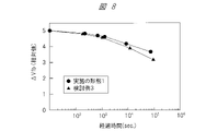
以下に、上述のようなリテンション特性の向上について、図5~図8および図27~図29を用いて詳しく説明する。
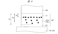
距離Xを図6の距離Xa~Xcに当てはめた場合、X=Xaの時には、変動量ΔVfbはほぼ一定となる。X=Xbの時には、電荷蓄積層CSLの膜中において距離Xbが変化するので、変動量ΔVfbはXbの積分値(∫Xbdx)に比例する。すなわち、変動量ΔVfbはXbの2乗(Xb2)に比例する。X=Xcの時には、変動量ΔVfbはXcに比例する。
以下に、図9~図13を用いて、本実施の形態の半導体装置の製造方法を説明する。
以下に、実施の形態2の半導体装置を、図14を用いて説明する。なお、以下の説明では、実施の形態1との相違点を主に説明する。図14は、実施の形態2の半導体装置の要部を拡大した断面図であり、ゲート絶縁膜MZの詳細な構造を示す断面図である。
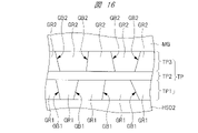
以下に、実施の形態3の半導体装置を、図15および図16を用いて説明する。なお、以下の説明では、実施の形態1との相違点を主に説明する。図15は、実施の形態3の半導体装置の要部を拡大した断面図であり、ゲート絶縁膜MZの詳細な構造を示す断面図である。図16は、ゲート絶縁膜MZのうちの一部を拡大し、絶縁膜TPの詳細な構造を示す断面図である。
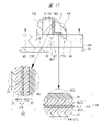
以下に、実施の形態4の半導体装置を図17~図19を用いて説明し、実施の形態4の半導体装置の製造方法を図20~図25を用いて説明する。なお、以下の説明では、実施の形態1との相違点を主に説明する。
図17に示されるように、半導体基板SBには、p型のウェル領域PWが形成されている。ウェル領域PW上には、ゲート絶縁膜GFが形成され、ゲート絶縁膜GF上には、制御ゲート電極CGが形成されている。ゲート絶縁膜GFは、例えば酸化シリコン膜であり、例えば2nm~5nmの厚さを有する。ゲート絶縁膜GFは、酸化シリコン膜に代えて、酸化ハフニウム膜などの酸化金属膜のような高誘電率膜であってもよい。制御ゲート電極CGは、例えばn型の不純物が導入された多結晶シリコン膜である。また、制御ゲート電極CGは、例えば窒化チタン膜、アルミニウム膜若しくはタングステン膜のような金属膜、または、これらの金属膜の積層膜であってもよい。
次に、不揮発性メモリセルであるメモリセルMC2の動作例について、図18および図19を参照して説明する。なお、ここで説明するメモリセルMC2は、半導体装置内に存在している複数のメモリセルMC2のうち、選択メモリセルである。
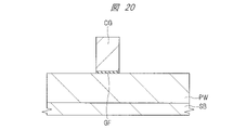
以下に、図20~図25を用いて、実施の形態4の半導体装置の製造方法を説明する。
以下に、実施の形態4の変形例の半導体装置を、図26を用いて説明する。なお、以下の説明では、実施の形態4との相違点を主に説明する。
BT 絶縁膜(ボトム絶縁膜)
CG 制御ゲート電極
CSL 電荷蓄積層
EXD エクステンション領域
EXS エクステンション領域
GB1、GB2 粒界
GF ゲート絶縁膜
GR1、GR2 結晶粒
HO 絶縁膜
HSO1~HSO3 絶縁膜
IF1 絶縁膜
IL1、IL2 層間絶縁膜
MC1~MC3 メモリセル
MD 拡散領域
MG メモリゲート電極
MS 拡散領域
MZ ゲート絶縁膜
PG プラグ
PW ウェル領域
SB 半導体基板
SI シリサイド層
SW サイドウォールスペーサ
TP 絶縁膜(トップ絶縁膜)
TP1~TP3 絶縁膜
Claims (13)
- 半導体基板上に形成され、且つ、電荷の保持が可能な電荷蓄積層を含む第1ゲート絶縁膜と、前記第1ゲート絶縁膜上に形成された第1ゲート電極とを有する不揮発性メモリセルを備える半導体装置であって、
前記電荷蓄積層は、
前記半導体基板上に形成され、且つ、ハフニウムシリケート膜からなる第1絶縁膜と、
前記第1絶縁膜上に形成され、前記第1絶縁膜とは異なる材料からなり、且つ、アルミニウム膜、窒化アルミニウム膜、炭化アルミニウム膜、アルミニウムシリケート膜または酸化アルミニウム膜からなる第1挿入層と、
前記第1挿入層上に形成され、前記第1挿入層とは異なる材料からなり、且つ、ハフニウムシリケート膜からなる第2絶縁膜と、
を有する、半導体装置。 - 請求項1に記載の半導体装置において、
前記第1挿入層の厚さは、前記第1絶縁膜の厚さおよび前記第2絶縁膜の厚さよりも薄い、半導体装置。 - 請求項1に記載の半導体装置において、
前記第1ゲート絶縁膜は、前記半導体基板と前記電荷蓄積層との間に、酸化シリコン膜または酸窒化シリコン膜からなる第3絶縁膜を更に有し、
前記第1絶縁膜は、前記第3絶縁膜に直接接している、半導体装置。 - 請求項3に記載の半導体装置において、
前記電荷蓄積層は、
前記第2絶縁膜上に形成され、且つ、前記第1挿入層と同じ膜からなる第2挿入層と、
前記第2挿入層上に形成され、前記第2挿入層とは異なる材料からなり、且つ、ハフニウムシリケート膜からなる第4絶縁膜と、
を更に有する、半導体装置。 - 請求項1に記載の半導体装置において、
前記第1ゲート絶縁膜は、前記電荷蓄積層と前記第1ゲート電極との間に、酸化アルミニウム膜、酸窒化アルミニウム膜またはアルミニウムシリケート膜からなり、且つ、前記第1挿入層よりも厚い厚さを有する第3絶縁膜を更に有する、半導体装置。 - 請求項1に記載の半導体装置において、
前記第1ゲート絶縁膜は、前記第1ゲート電極と前記電荷蓄積層との間に、第3絶縁膜を更に有し、
前記第3絶縁膜は、
前記電荷蓄積層上に形成され、且つ、酸化アルミニウム膜、酸窒化アルミニウム膜またはアルミニウムシリケート膜からなる第4絶縁膜と、
前記第4絶縁膜上に形成され、且つ、酸化シリコン膜、酸窒化シリコン膜または窒化シリコン膜からなる第5絶縁膜と、
前記第5絶縁膜上に形成され、且つ、酸化アルミニウム膜、酸窒化アルミニウム膜またはアルミニウムシリケート膜からなる第6絶縁膜と、
を有し、
前記第1挿入層の厚さは、前記第4絶縁膜の厚さおよび前記第6絶縁膜の厚さよりも薄い、半導体装置。 - 請求項6に記載の半導体装置において、
前記第4絶縁膜に含まれる複数の第1結晶粒と、前記第6絶縁膜に含まれる複数の第2結晶粒とは、前記第5絶縁膜によって分離されている、半導体装置。 - 請求項7に記載の半導体装置において、
前記第4絶縁膜および前記第6絶縁膜は、それぞれ多結晶膜であり、
前記第5絶縁膜は、非晶質膜である、半導体装置。 - 請求項1に記載の半導体装置において、
前記不揮発性メモリセルは、
前記半導体基板上に形成された第2ゲート絶縁膜と、
前記第2ゲート絶縁膜上に形成された第2ゲート電極と、
を更に有し、
前記第1ゲート電極は、前記第2ゲート電極と絶縁分離されている、半導体装置。 - 請求項1に記載の半導体装置において、
前記第1挿入層は、酸化アルミニウム膜からなる、半導体装置。 - (a)半導体基板上に、電荷の保持が可能な電荷蓄積層を含む第1ゲート絶縁膜を形成する工程、
(b)前記第1ゲート絶縁膜上に、第1ゲート電極を形成する工程、
を有し、
前記(a)工程において、前記電荷蓄積層を形成する工程は、
(a1)前記半導体基板上に、ハフニウムシリケート膜からなる第1絶縁膜を形成する工程、
(a2)前記第1絶縁膜上に、アルミニウム膜、窒化アルミニウム膜、炭化アルミニウム膜、アルミニウムシリケート膜または酸化アルミニウム膜からなる第1挿入層を形成する工程、
(a3)前記第1挿入層上に、ハフニウムシリケート膜からなる第2絶縁膜を形成する工程、
を有する、半導体装置の製造方法。 - 請求項11に記載の半導体装置の製造方法において、
前記(a3)工程後、熱処理を行う工程、を更に有し、
前記第1絶縁膜および前記第2絶縁膜の各々の前記ハフニウムシリケート膜は、HfxSi1-xO2(0<x<1)膜であり、
0.9≦x<1である場合には、前記熱処理の温度を800℃以上、975℃未満とし、
0<x<0.9である場合には、前記熱処理の温度を975℃以上、1050℃以下とする、半導体装置の製造方法。 - 請求項11に記載の半導体装置の製造方法において、
前記(a)工程において、前記電荷蓄積層を形成する工程は、
(a4)前記第2絶縁膜上に、前記第2絶縁膜の厚さよりも薄い厚さを有し、且つ、アルミニウム膜、窒化アルミニウム膜、炭化アルミニウム膜、アルミニウムシリケート膜または酸化アルミニウム膜からなる第2挿入層を形成する工程、
(a5)前記第2挿入層上に、前記第2挿入層の厚さよりも厚い厚さを有し、且つ、ハフニウムシリケート膜からなる第3絶縁膜を形成する工程、
を更に有する、半導体装置の製造方法。
Priority Applications (4)
| Application Number | Priority Date | Filing Date | Title |
|---|---|---|---|
| JP2018134089A JP7089967B2 (ja) | 2018-07-17 | 2018-07-17 | 半導体装置およびその製造方法 |
| CN201910521429.8A CN110729301A (zh) | 2018-07-17 | 2019-06-17 | 半导体器件及其制造方法 |
| US16/452,261 US11094833B2 (en) | 2018-07-17 | 2019-06-25 | Semiconductor device including memory using hafnium and a method of manufacturing the same |
| TW108122298A TWI822805B (zh) | 2018-07-17 | 2019-06-26 | 半導體元件及其製造方法 |
Applications Claiming Priority (1)
| Application Number | Priority Date | Filing Date | Title |
|---|---|---|---|
| JP2018134089A JP7089967B2 (ja) | 2018-07-17 | 2018-07-17 | 半導体装置およびその製造方法 |
Publications (3)
| Publication Number | Publication Date |
|---|---|
| JP2020013850A JP2020013850A (ja) | 2020-01-23 |
| JP2020013850A5 JP2020013850A5 (ja) | 2021-03-04 |
| JP7089967B2 true JP7089967B2 (ja) | 2022-06-23 |
Family
ID=69161350
Family Applications (1)
| Application Number | Title | Priority Date | Filing Date |
|---|---|---|---|
| JP2018134089A Active JP7089967B2 (ja) | 2018-07-17 | 2018-07-17 | 半導体装置およびその製造方法 |
Country Status (4)
| Country | Link |
|---|---|
| US (1) | US11094833B2 (ja) |
| JP (1) | JP7089967B2 (ja) |
| CN (1) | CN110729301A (ja) |
| TW (1) | TWI822805B (ja) |
Families Citing this family (1)
| Publication number | Priority date | Publication date | Assignee | Title |
|---|---|---|---|---|
| US20210305258A1 (en) * | 2020-03-31 | 2021-09-30 | Taiwan Semiconductor Manufacturing Co., Ltd. | Multi-Layer High-K Gate Dielectric Structure |
Citations (2)
| Publication number | Priority date | Publication date | Assignee | Title |
|---|---|---|---|---|
| US20080237688A1 (en) | 2007-03-27 | 2008-10-02 | Naoki Yasuda | Memory cell of nonvolatile semiconductor memory |
| US20150060991A1 (en) | 2013-09-05 | 2015-03-05 | Renesas Electronics Corporation | Semiconductor device and method of manufacturing the same |
Family Cites Families (120)
| Publication number | Priority date | Publication date | Assignee | Title |
|---|---|---|---|---|
| JP2002280465A (ja) * | 2001-03-19 | 2002-09-27 | Sony Corp | 不揮発性半導体記憶装置およびその製造方法 |
| US20030235961A1 (en) * | 2002-04-17 | 2003-12-25 | Applied Materials, Inc. | Cyclical sequential deposition of multicomponent films |
| US7135421B2 (en) * | 2002-06-05 | 2006-11-14 | Micron Technology, Inc. | Atomic layer-deposited hafnium aluminum oxide |
| JP3987418B2 (ja) * | 2002-11-15 | 2007-10-10 | 株式会社東芝 | 半導体記憶装置 |
| US6706599B1 (en) * | 2003-03-20 | 2004-03-16 | Motorola, Inc. | Multi-bit non-volatile memory device and method therefor |
| JP4507232B2 (ja) * | 2003-03-24 | 2010-07-21 | ローム株式会社 | 半導体装置の製造方法 |
| US7098502B2 (en) * | 2003-11-10 | 2006-08-29 | Freescale Semiconductor, Inc. | Transistor having three electrically isolated electrodes and method of formation |
| JP2005294791A (ja) * | 2004-03-09 | 2005-10-20 | Nec Corp | 不揮発性メモリ及び不揮発性メモリの製造方法 |
| US8323754B2 (en) * | 2004-05-21 | 2012-12-04 | Applied Materials, Inc. | Stabilization of high-k dielectric materials |
| JP4419699B2 (ja) * | 2004-06-16 | 2010-02-24 | ソニー株式会社 | 不揮発性半導体メモリ装置およびその動作方法 |
| JP4296128B2 (ja) * | 2004-06-23 | 2009-07-15 | 株式会社東芝 | 不揮発性半導体メモリ装置及びその製造方法 |
| KR100673001B1 (ko) * | 2005-04-04 | 2007-01-24 | 삼성전자주식회사 | 비휘발성 메모리 장치 및 그 제조방법 |
| US7576386B2 (en) * | 2005-08-04 | 2009-08-18 | Macronix International Co., Ltd. | Non-volatile memory semiconductor device having an oxide-nitride-oxide (ONO) top dielectric layer |
| US7402534B2 (en) * | 2005-08-26 | 2008-07-22 | Applied Materials, Inc. | Pretreatment processes within a batch ALD reactor |
| KR100660551B1 (ko) * | 2005-09-22 | 2006-12-22 | 삼성전자주식회사 | 불휘발성 메모리 소자 및 그 제조 방법 |
| JP2007305788A (ja) * | 2006-05-11 | 2007-11-22 | Toshiba Corp | 半導体記憶装置 |
| JP2008060538A (ja) * | 2006-07-31 | 2008-03-13 | Toshiba Corp | 半導体装置およびその製造方法 |
| KR100816755B1 (ko) * | 2006-10-19 | 2008-03-25 | 삼성전자주식회사 | 플래시 메모리 장치 및 그 제조방법 |
| KR100843550B1 (ko) * | 2006-11-06 | 2008-07-04 | 삼성전자주식회사 | 비휘발성 메모리 장치 및 그 제조방법 |
| US8686490B2 (en) * | 2006-12-20 | 2014-04-01 | Sandisk Corporation | Electron blocking layers for electronic devices |
| US20080150009A1 (en) * | 2006-12-20 | 2008-06-26 | Nanosys, Inc. | Electron Blocking Layers for Electronic Devices |
| US7479429B2 (en) * | 2007-01-31 | 2009-01-20 | Freescale Semiconductor, Inc. | Split game memory cell method |
| KR100851552B1 (ko) * | 2007-03-28 | 2008-08-11 | 삼성전자주식회사 | 비휘발성 기억 소자 및 그 형성 방법 |
| KR100855993B1 (ko) * | 2007-04-03 | 2008-09-02 | 삼성전자주식회사 | 전하 트랩 플래시 메모리 소자 및 그 제조방법 |
| TW200843121A (en) * | 2007-04-24 | 2008-11-01 | Nanya Technology Corp | Two-bit flash memory cell and method for manufacturing the same |
| KR20080104783A (ko) * | 2007-05-29 | 2008-12-03 | 삼성전자주식회사 | 비휘발성 기억 소자의 형성 방법 |
| JP2009010104A (ja) * | 2007-06-27 | 2009-01-15 | Renesas Technology Corp | 半導体装置およびその製造方法 |
| KR100886643B1 (ko) * | 2007-07-02 | 2009-03-04 | 주식회사 하이닉스반도체 | 비휘발성 메모리 소자 및 그 제조방법 |
| KR101108709B1 (ko) * | 2007-07-12 | 2012-01-30 | 삼성전자주식회사 | 반도체 장치 및 반도체 장치의 제조 방법 |
| KR101338166B1 (ko) * | 2007-07-12 | 2013-12-06 | 삼성전자주식회사 | 비휘발성 기억 소자 및 그 소자의 형성 방법 |
| JP2009054951A (ja) * | 2007-08-29 | 2009-03-12 | Toshiba Corp | 不揮発性半導体記憶素子及びその製造方法 |
| JP5238208B2 (ja) * | 2007-09-27 | 2013-07-17 | 株式会社東芝 | 不揮発性半導体記憶装置の駆動方法及び不揮発性半導体記憶装置 |
| KR101404669B1 (ko) * | 2007-09-27 | 2014-06-09 | 삼성전자주식회사 | 비휘발성 메모리 장치 및 그 형성 방법 |
| US8159012B2 (en) * | 2007-09-28 | 2012-04-17 | Samsung Electronics Co., Ltd. | Semiconductor device including insulating layer of cubic system or tetragonal system |
| JP5129541B2 (ja) * | 2007-10-15 | 2013-01-30 | ルネサスエレクトロニクス株式会社 | 半導体装置およびその製造方法 |
| JP5196954B2 (ja) * | 2007-10-31 | 2013-05-15 | 株式会社東芝 | 半導体装置の製造方法 |
| KR20090052682A (ko) * | 2007-11-21 | 2009-05-26 | 삼성전자주식회사 | 비휘발성 메모리 소자 및 이를 포함하는 카드 및 시스템 |
| KR20090055202A (ko) * | 2007-11-28 | 2009-06-02 | 삼성전자주식회사 | 플래시 메모리 소자 및 이를 포함하는 카드 및 시스템 |
| JP5521555B2 (ja) * | 2008-02-20 | 2014-06-18 | 日本電気株式会社 | 不揮発性記憶装置およびその製造方法 |
| JP5279312B2 (ja) * | 2008-03-28 | 2013-09-04 | 株式会社東芝 | 半導体装置、及び半導体装置の製造方法 |
| US7659158B2 (en) * | 2008-03-31 | 2010-02-09 | Applied Materials, Inc. | Atomic layer deposition processes for non-volatile memory devices |
| KR101458957B1 (ko) * | 2008-06-17 | 2014-11-10 | 삼성전자주식회사 | 선택 트랜지스터 및 그의 제조 방법 |
| KR20100000652A (ko) * | 2008-06-25 | 2010-01-06 | 삼성전자주식회사 | 비휘발성 메모리 소자, 이를 포함하는 메모리 카드 및시스템 |
| JP5406479B2 (ja) * | 2008-08-01 | 2014-02-05 | ルネサスエレクトロニクス株式会社 | 半導体装置の製造方法 |
| JP5355980B2 (ja) * | 2008-09-29 | 2013-11-27 | 株式会社東芝 | 不揮発性半導体記憶装置及びその駆動方法 |
| KR101514784B1 (ko) * | 2008-11-24 | 2015-04-27 | 삼성전자주식회사 | 비휘발성 메모리 소자 |
| KR20100081833A (ko) * | 2009-01-07 | 2010-07-15 | 삼성전자주식회사 | 비휘발성 메모리 소자의 제조 방법 |
| JP5336872B2 (ja) * | 2009-02-06 | 2013-11-06 | 株式会社東芝 | 不揮発性半導体記憶装置及びその製造方法 |
| KR20100100550A (ko) * | 2009-03-06 | 2010-09-15 | 삼성전자주식회사 | 메모리 장치의 제조 방법 |
| KR101583608B1 (ko) * | 2009-03-24 | 2016-01-08 | 삼성전자 주식회사 | 무기계 실리콘 전구체를 이용한 실리콘 산화막의 형성 방법및 이를 이용한 반도체 장치의 제조 방법 |
| JP5281455B2 (ja) * | 2009-03-26 | 2013-09-04 | 株式会社東芝 | 不揮発性半導体記憶装置及びその駆動方法 |
| US8263463B2 (en) * | 2009-03-30 | 2012-09-11 | Freescale Semiconductor, Inc. | Nonvolatile split gate memory cell having oxide growth |
| US7821055B2 (en) * | 2009-03-31 | 2010-10-26 | Freescale Semiconductor, Inc. | Stressed semiconductor device and method for making |
| US7960267B2 (en) * | 2009-03-31 | 2011-06-14 | Freescale Semiconductor, Inc. | Method for making a stressed non-volatile memory device |
| KR20100133676A (ko) * | 2009-06-12 | 2010-12-22 | 삼성전자주식회사 | 경사 이온 주입을 이용한 비휘발성 메모리 장치의 제조 방법 |
| JP2011054843A (ja) * | 2009-09-03 | 2011-03-17 | Panasonic Corp | 半導体装置及びその製造方法 |
| JP5524632B2 (ja) * | 2010-01-18 | 2014-06-18 | ルネサスエレクトロニクス株式会社 | 半導体記憶装置 |
| JP2011159364A (ja) * | 2010-02-02 | 2011-08-18 | Toshiba Corp | 不揮発性半導体記憶装置および不揮発性半導体記憶装置の駆動方法 |
| JP5378255B2 (ja) * | 2010-02-02 | 2013-12-25 | 株式会社東芝 | 不揮発性半導体記憶装置および不揮発性半導体記憶装置の駆動方法 |
| WO2011114502A1 (ja) * | 2010-03-19 | 2011-09-22 | 株式会社 東芝 | 不揮発性半導体記憶装置及びその製造方法 |
| WO2011114503A1 (ja) * | 2010-03-19 | 2011-09-22 | 株式会社 東芝 | 不揮発性半導体記憶装置及びその製造方法 |
| JP2011199131A (ja) * | 2010-03-23 | 2011-10-06 | Toshiba Corp | 不揮発性半導体記憶装置及びその製造方法 |
| KR20110106688A (ko) * | 2010-03-23 | 2011-09-29 | 삼성전자주식회사 | 비휘발성 메모리 소자 |
| KR20110106682A (ko) * | 2010-03-23 | 2011-09-29 | 삼성전자주식회사 | 수직형 융합 반도체 장치 |
| KR101738533B1 (ko) * | 2010-05-24 | 2017-05-23 | 삼성전자 주식회사 | 적층 메모리 장치 및 그 제조 방법 |
| US8455940B2 (en) * | 2010-05-24 | 2013-06-04 | Samsung Electronics Co., Ltd. | Nonvolatile memory device, method of manufacturing the nonvolatile memory device, and memory module and system including the nonvolatile memory device |
| KR101652829B1 (ko) * | 2010-06-03 | 2016-09-01 | 삼성전자주식회사 | 수직 구조의 비휘발성 메모리 소자 |
| KR101660432B1 (ko) * | 2010-06-07 | 2016-09-27 | 삼성전자 주식회사 | 수직 구조의 반도체 메모리 소자 |
| KR20120003169A (ko) * | 2010-07-02 | 2012-01-10 | 삼성전자주식회사 | 고선택비 식각액 및 이를 이용한 반도체 소자의 제조 방법 |
| KR20120019208A (ko) * | 2010-08-25 | 2012-03-06 | 삼성전자주식회사 | 비휘발성 메모리 장치의 제조 방법 |
| JP5624415B2 (ja) * | 2010-09-21 | 2014-11-12 | 株式会社東芝 | 不揮発性半導体記憶装置及びその製造方法 |
| JP5651415B2 (ja) * | 2010-09-21 | 2015-01-14 | 株式会社東芝 | 不揮発性半導体記憶装置及びその製造方法 |
| JP2012160222A (ja) * | 2011-01-31 | 2012-08-23 | Toshiba Corp | 不揮発性半導体記憶装置 |
| JP2012168999A (ja) * | 2011-02-10 | 2012-09-06 | Toshiba Corp | 不揮発性半導体記憶装置の動作方法 |
| KR101809512B1 (ko) * | 2011-03-09 | 2017-12-15 | 삼성전자 주식회사 | 비휘발성 메모리 소자 및 그 제조 방법 |
| KR101845508B1 (ko) * | 2011-04-27 | 2018-04-05 | 삼성전자주식회사 | 반도체 소자의 제조 방법 |
| JP2012234885A (ja) * | 2011-04-28 | 2012-11-29 | Toshiba Corp | 半導体装置及びその製造方法 |
| KR101916222B1 (ko) * | 2011-04-29 | 2018-11-08 | 삼성전자 주식회사 | 수직 구조의 비휘발성 메모리 소자 및 그 제조 방법 |
| KR101845507B1 (ko) * | 2011-05-03 | 2018-04-05 | 삼성전자주식회사 | 수직 구조의 비휘발성 메모리 소자 및 그 제조 방법 |
| JP2013026289A (ja) * | 2011-07-15 | 2013-02-04 | Toshiba Corp | 不揮発性半導体記憶装置及びその製造方法 |
| JP5674579B2 (ja) * | 2011-07-15 | 2015-02-25 | 株式会社東芝 | 不揮発性半導体記憶装置及びその製造方法 |
| KR101845511B1 (ko) * | 2011-10-11 | 2018-04-05 | 삼성전자주식회사 | 수직 구조의 비휘발성 메모리 소자 제조 방법 |
| JP5694129B2 (ja) * | 2011-11-29 | 2015-04-01 | 株式会社東芝 | 半導体装置及びその製造方法 |
| JP5624567B2 (ja) * | 2012-02-03 | 2014-11-12 | 株式会社東芝 | 不揮発性半導体記憶装置及びその製造方法 |
| JP2013239622A (ja) * | 2012-05-16 | 2013-11-28 | Toshiba Corp | 不揮発性半導体記憶装置及びその製造方法 |
| US8779498B2 (en) * | 2012-09-05 | 2014-07-15 | Kabushiki Kaisha Toshiba | Nonvolatile semiconductor memory device |
| US8896052B2 (en) * | 2012-09-05 | 2014-11-25 | Kabushiki Kaisha Toshiba | Nonvolatile semiconductor memory device and method of manufacturing the same |
| JP5956972B2 (ja) * | 2012-12-21 | 2016-07-27 | 東京エレクトロン株式会社 | 成膜方法 |
| JP2014179530A (ja) * | 2013-03-15 | 2014-09-25 | Toshiba Corp | 不揮発性半導体記憶装置の製造方法 |
| US8921923B2 (en) * | 2013-03-18 | 2014-12-30 | Kabushiki Kaisha Toshiba | Method for manufacturing semiconductor memory device and semiconductor memory device |
| JP2015015287A (ja) * | 2013-07-03 | 2015-01-22 | 株式会社東芝 | 不揮発性半導体記憶装置及びその製造方法 |
| KR102039708B1 (ko) * | 2013-11-13 | 2019-11-01 | 삼성전자주식회사 | 비휘발성 메모리 장치 및 그 제조 방법 |
| KR20150057147A (ko) * | 2013-11-18 | 2015-05-28 | 삼성전자주식회사 | 메모리 장치 |
| US8953380B1 (en) * | 2013-12-02 | 2015-02-10 | Cypress Semiconductor Corporation | Systems, methods, and apparatus for memory cells with common source lines |
| KR102198856B1 (ko) * | 2014-02-10 | 2021-01-05 | 삼성전자 주식회사 | 니켈 함유막을 포함하는 반도체 소자의 제조 방법 |
| JP2015167200A (ja) * | 2014-03-04 | 2015-09-24 | 株式会社東芝 | 不揮発性半導体記憶装置 |
| KR102171025B1 (ko) * | 2014-04-30 | 2020-10-29 | 삼성전자주식회사 | 비휘발성 메모리 장치 |
| JP6334268B2 (ja) * | 2014-05-30 | 2018-05-30 | ルネサスエレクトロニクス株式会社 | 半導体装置およびその製造方法 |
| KR20160000512A (ko) * | 2014-06-24 | 2016-01-05 | 삼성전자주식회사 | 메모리 장치 |
| KR102263315B1 (ko) * | 2014-08-06 | 2021-06-15 | 삼성전자주식회사 | 반도체 장치 및 반도체 장치의 제조방법 |
| KR102240024B1 (ko) * | 2014-08-22 | 2021-04-15 | 삼성전자주식회사 | 반도체 장치, 반도체 장치의 제조방법 및 에피택시얼층의 형성방법 |
| KR102238257B1 (ko) * | 2014-08-26 | 2021-04-13 | 삼성전자주식회사 | 반도체 소자의 제조 방법 |
| KR20160029236A (ko) * | 2014-09-04 | 2016-03-15 | 삼성전자주식회사 | 반도체 장치 및 그 제조 방법 |
| KR102244219B1 (ko) * | 2014-09-29 | 2021-04-27 | 삼성전자주식회사 | 메모리 장치 및 그 제조 방법 |
| KR102342549B1 (ko) * | 2015-06-05 | 2021-12-24 | 삼성전자주식회사 | 메모리 장치 및 그 제조 방법 |
| JP6416053B2 (ja) * | 2015-07-31 | 2018-10-31 | 東芝メモリ株式会社 | 不揮発性半導体記憶装置 |
| KR102423765B1 (ko) * | 2015-08-26 | 2022-07-21 | 삼성전자주식회사 | 수직 구조의 비휘발성 메모리 소자 및 그 제조 방법 |
| KR102421728B1 (ko) * | 2015-09-10 | 2022-07-18 | 삼성전자주식회사 | 메모리 장치 및 그 제조 방법 |
| JP2017054941A (ja) * | 2015-09-10 | 2017-03-16 | 株式会社東芝 | 半導体装置及びその製造方法 |
| KR102565716B1 (ko) * | 2015-12-24 | 2023-08-11 | 삼성전자주식회사 | 메모리 장치 |
| US10157933B2 (en) * | 2016-04-19 | 2018-12-18 | Micron Technology, Inc. | Integrated structures including material containing silicon, nitrogen, and at least one of carbon, oxygen, boron and phosphorus |
| US9853049B2 (en) * | 2016-04-21 | 2017-12-26 | Samsung Electronics Co., Ltd. | Memory devices having common source lines including layers of different materials |
| KR102637644B1 (ko) * | 2016-07-14 | 2024-02-19 | 삼성전자주식회사 | 메모리 장치 |
| KR102619876B1 (ko) * | 2016-07-19 | 2024-01-03 | 삼성전자주식회사 | 메모리 장치 |
| KR20180010368A (ko) * | 2016-07-20 | 2018-01-31 | 삼성전자주식회사 | 메모리 장치 |
| KR20180034798A (ko) * | 2016-09-28 | 2018-04-05 | 삼성전자주식회사 | 유전막 형성 방법 및 반도체 장치의 제조 방법 |
| US9842845B1 (en) * | 2016-10-28 | 2017-12-12 | Globalfoundries Inc. | Method of forming a semiconductor device structure and semiconductor device structure |
| US10049882B1 (en) * | 2017-01-25 | 2018-08-14 | Samsung Electronics Co., Ltd. | Method for fabricating semiconductor device including forming a dielectric layer on a structure having a height difference using ALD |
| JP6877319B2 (ja) * | 2017-11-15 | 2021-05-26 | ルネサスエレクトロニクス株式会社 | 半導体装置およびその製造方法 |
| JP2019192719A (ja) * | 2018-04-20 | 2019-10-31 | ルネサスエレクトロニクス株式会社 | 半導体装置およびその製造方法 |
-
2018
- 2018-07-17 JP JP2018134089A patent/JP7089967B2/ja active Active
-
2019
- 2019-06-17 CN CN201910521429.8A patent/CN110729301A/zh active Pending
- 2019-06-25 US US16/452,261 patent/US11094833B2/en active Active
- 2019-06-26 TW TW108122298A patent/TWI822805B/zh active
Patent Citations (4)
| Publication number | Priority date | Publication date | Assignee | Title |
|---|---|---|---|---|
| US20080237688A1 (en) | 2007-03-27 | 2008-10-02 | Naoki Yasuda | Memory cell of nonvolatile semiconductor memory |
| JP2008244163A (ja) | 2007-03-27 | 2008-10-09 | Toshiba Corp | 不揮発性半導体メモリのメモリセル |
| US20150060991A1 (en) | 2013-09-05 | 2015-03-05 | Renesas Electronics Corporation | Semiconductor device and method of manufacturing the same |
| JP2015053474A (ja) | 2013-09-05 | 2015-03-19 | ルネサスエレクトロニクス株式会社 | 半導体装置およびその製造方法 |
Also Published As
| Publication number | Publication date |
|---|---|
| CN110729301A (zh) | 2020-01-24 |
| TWI822805B (zh) | 2023-11-21 |
| TW202006925A (zh) | 2020-02-01 |
| US20200027996A1 (en) | 2020-01-23 |
| US11094833B2 (en) | 2021-08-17 |
| JP2020013850A (ja) | 2020-01-23 |
Similar Documents
| Publication | Publication Date | Title |
|---|---|---|
| US10229925B2 (en) | Semiconductor device and method of manufacturing the same | |
| JP5472894B2 (ja) | 不揮発性半導体記憶装置 | |
| JP5592214B2 (ja) | 半導体装置の製造方法 | |
| JP5781733B2 (ja) | 不揮発性メモリセル及びその製造方法 | |
| JP6998267B2 (ja) | 半導体装置およびその製造方法 | |
| JP5221065B2 (ja) | 不揮発性半導体メモリ装置 | |
| JP6778607B2 (ja) | 半導体装置の製造方法 | |
| US11133422B2 (en) | Method for manufacturing a semiconductor device | |
| JP2009252774A (ja) | 半導体記憶装置およびその製造方法 | |
| WO2016088196A1 (ja) | 半導体装置の製造方法および半導体装置 | |
| JP7089967B2 (ja) | 半導体装置およびその製造方法 | |
| JP7042726B2 (ja) | 半導体装置の製造方法 | |
| JP5132330B2 (ja) | 不揮発性半導体記憶装置およびその製造方法 | |
| JP2010135561A (ja) | 不揮発性半導体記憶装置 | |
| US20220157964A1 (en) | Semiconductor device | |
| US20220157999A1 (en) | Semiconductor device | |
| US11563111B2 (en) | Method of manufacturing semiconductor device having split-gate memory and MISFET | |
| CN116648066A (zh) | 制造半导体器件的方法 | |
| JP2022082914A (ja) | 半導体装置およびその製造方法 | |
| JP2010021186A (ja) | 半導体装置及びその製造方法 | |
| JP2016157728A (ja) | 半導体装置の製造方法 |
Legal Events
| Date | Code | Title | Description |
|---|---|---|---|
| A521 | Request for written amendment filed |
Free format text: JAPANESE INTERMEDIATE CODE: A523 Effective date: 20210115 |
|
| A621 | Written request for application examination |
Free format text: JAPANESE INTERMEDIATE CODE: A621 Effective date: 20210115 |
|
| A131 | Notification of reasons for refusal |
Free format text: JAPANESE INTERMEDIATE CODE: A131 Effective date: 20211026 |
|
| A977 | Report on retrieval |
Free format text: JAPANESE INTERMEDIATE CODE: A971007 Effective date: 20211029 |
|
| A521 | Request for written amendment filed |
Free format text: JAPANESE INTERMEDIATE CODE: A523 Effective date: 20211217 |
|
| A131 | Notification of reasons for refusal |
Free format text: JAPANESE INTERMEDIATE CODE: A131 Effective date: 20220208 |
|
| A521 | Request for written amendment filed |
Free format text: JAPANESE INTERMEDIATE CODE: A523 Effective date: 20220404 |
|
| TRDD | Decision of grant or rejection written | ||
| A01 | Written decision to grant a patent or to grant a registration (utility model) |
Free format text: JAPANESE INTERMEDIATE CODE: A01 Effective date: 20220524 |
|
| A61 | First payment of annual fees (during grant procedure) |
Free format text: JAPANESE INTERMEDIATE CODE: A61 Effective date: 20220613 |
|
| R150 | Certificate of patent or registration of utility model |
Ref document number: 7089967 Country of ref document: JP Free format text: JAPANESE INTERMEDIATE CODE: R150 |