EP2842003B1 - Affichage grand angle holographique - Google Patents
Affichage grand angle holographique Download PDFInfo
- Publication number
- EP2842003B1 EP2842003B1 EP13765610.4A EP13765610A EP2842003B1 EP 2842003 B1 EP2842003 B1 EP 2842003B1 EP 13765610 A EP13765610 A EP 13765610A EP 2842003 B1 EP2842003 B1 EP 2842003B1
- Authority
- EP
- European Patent Office
- Prior art keywords
- elements
- multiplicity
- grating
- grating elements
- bragg grating
- Prior art date
- Legal status (The legal status is an assumption and is not a legal conclusion. Google has not performed a legal analysis and makes no representation as to the accuracy of the status listed.)
- Active
Links
- 210000001747 pupil Anatomy 0.000 claims description 142
- 238000000034 method Methods 0.000 claims description 35
- 230000000737 periodic effect Effects 0.000 claims description 13
- 239000010432 diamond Substances 0.000 claims description 10
- 229910003460 diamond Inorganic materials 0.000 claims description 8
- 230000001419 dependent effect Effects 0.000 claims description 4
- 239000010410 layer Substances 0.000 description 147
- 230000000694 effects Effects 0.000 description 70
- 239000000758 substrate Substances 0.000 description 48
- 238000013461 design Methods 0.000 description 45
- 230000003287 optical effect Effects 0.000 description 41
- 238000010586 diagram Methods 0.000 description 30
- 238000005286 illumination Methods 0.000 description 30
- 230000005540 biological transmission Effects 0.000 description 22
- 238000010168 coupling process Methods 0.000 description 22
- 238000005859 coupling reaction Methods 0.000 description 22
- 230000008878 coupling Effects 0.000 description 20
- 238000004458 analytical method Methods 0.000 description 16
- 230000006870 function Effects 0.000 description 15
- 230000010287 polarization Effects 0.000 description 14
- 239000000463 material Substances 0.000 description 13
- 238000009826 distribution Methods 0.000 description 12
- 230000008901 benefit Effects 0.000 description 11
- 239000004973 liquid crystal related substance Substances 0.000 description 11
- 239000010408 film Substances 0.000 description 10
- 238000003491 array Methods 0.000 description 9
- 208000013057 hereditary mucoepithelial dysplasia Diseases 0.000 description 9
- 230000008569 process Effects 0.000 description 9
- 239000013598 vector Substances 0.000 description 9
- 238000005516 engineering process Methods 0.000 description 8
- 239000005276 holographic polymer dispersed liquid crystals (HPDLCs) Substances 0.000 description 8
- 230000002829 reductive effect Effects 0.000 description 8
- 239000011521 glass Substances 0.000 description 7
- 230000000670 limiting effect Effects 0.000 description 7
- 239000004033 plastic Substances 0.000 description 7
- 229920003023 plastic Polymers 0.000 description 7
- 238000000576 coating method Methods 0.000 description 6
- 230000001965 increasing effect Effects 0.000 description 6
- 210000001525 retina Anatomy 0.000 description 6
- 230000002441 reversible effect Effects 0.000 description 6
- 238000013459 approach Methods 0.000 description 5
- 210000004027 cell Anatomy 0.000 description 5
- 239000002131 composite material Substances 0.000 description 5
- 230000003247 decreasing effect Effects 0.000 description 5
- 239000000203 mixture Substances 0.000 description 5
- 230000001902 propagating effect Effects 0.000 description 5
- 239000004983 Polymer Dispersed Liquid Crystal Substances 0.000 description 4
- 210000003128 head Anatomy 0.000 description 4
- 239000000178 monomer Substances 0.000 description 4
- 238000000059 patterning Methods 0.000 description 4
- 239000002356 single layer Substances 0.000 description 4
- 230000005684 electric field Effects 0.000 description 3
- 210000000887 face Anatomy 0.000 description 3
- 230000006872 improvement Effects 0.000 description 3
- 238000004519 manufacturing process Methods 0.000 description 3
- 238000011084 recovery Methods 0.000 description 3
- 238000005096 rolling process Methods 0.000 description 3
- 238000005070 sampling Methods 0.000 description 3
- 239000007787 solid Substances 0.000 description 3
- 239000000243 solution Substances 0.000 description 3
- 238000010521 absorption reaction Methods 0.000 description 2
- 239000012790 adhesive layer Substances 0.000 description 2
- 230000004075 alteration Effects 0.000 description 2
- 230000003466 anti-cipated effect Effects 0.000 description 2
- 230000015572 biosynthetic process Effects 0.000 description 2
- 230000008859 change Effects 0.000 description 2
- 238000005253 cladding Methods 0.000 description 2
- 239000011248 coating agent Substances 0.000 description 2
- 238000004891 communication Methods 0.000 description 2
- 230000007812 deficiency Effects 0.000 description 2
- 230000009977 dual effect Effects 0.000 description 2
- 238000000605 extraction Methods 0.000 description 2
- 238000000265 homogenisation Methods 0.000 description 2
- 238000003384 imaging method Methods 0.000 description 2
- 238000002347 injection Methods 0.000 description 2
- 239000007924 injection Substances 0.000 description 2
- 238000012986 modification Methods 0.000 description 2
- 230000004048 modification Effects 0.000 description 2
- 108091008695 photoreceptors Proteins 0.000 description 2
- 229920000642 polymer Polymers 0.000 description 2
- 230000009467 reduction Effects 0.000 description 2
- 238000002310 reflectometry Methods 0.000 description 2
- 230000004044 response Effects 0.000 description 2
- 239000010409 thin film Substances 0.000 description 2
- 230000004304 visual acuity Effects 0.000 description 2
- 238000012935 Averaging Methods 0.000 description 1
- 206010010071 Coma Diseases 0.000 description 1
- 241000761557 Lamina Species 0.000 description 1
- 230000003190 augmentative effect Effects 0.000 description 1
- 238000004364 calculation method Methods 0.000 description 1
- 210000002421 cell wall Anatomy 0.000 description 1
- 238000006243 chemical reaction Methods 0.000 description 1
- 230000001427 coherent effect Effects 0.000 description 1
- 230000002860 competitive effect Effects 0.000 description 1
- 230000001010 compromised effect Effects 0.000 description 1
- 238000011161 development Methods 0.000 description 1
- 238000009792 diffusion process Methods 0.000 description 1
- 238000006073 displacement reaction Methods 0.000 description 1
- 239000000428 dust Substances 0.000 description 1
- 239000000975 dye Substances 0.000 description 1
- 230000002708 enhancing effect Effects 0.000 description 1
- 230000004438 eyesight Effects 0.000 description 1
- 238000009501 film coating Methods 0.000 description 1
- 229920002457 flexible plastic Polymers 0.000 description 1
- 230000004907 flux Effects 0.000 description 1
- 230000004886 head movement Effects 0.000 description 1
- AMGQUBHHOARCQH-UHFFFAOYSA-N indium;oxotin Chemical compound [In].[Sn]=O AMGQUBHHOARCQH-UHFFFAOYSA-N 0.000 description 1
- 238000007689 inspection Methods 0.000 description 1
- 230000010354 integration Effects 0.000 description 1
- 230000003993 interaction Effects 0.000 description 1
- 230000001788 irregular Effects 0.000 description 1
- 238000003475 lamination Methods 0.000 description 1
- 239000011344 liquid material Substances 0.000 description 1
- 230000033001 locomotion Effects 0.000 description 1
- 230000007774 longterm Effects 0.000 description 1
- 238000002156 mixing Methods 0.000 description 1
- 230000008450 motivation Effects 0.000 description 1
- 230000010355 oscillation Effects 0.000 description 1
- 238000004806 packaging method and process Methods 0.000 description 1
- 238000005191 phase separation Methods 0.000 description 1
- 239000004417 polycarbonate Substances 0.000 description 1
- 229920000515 polycarbonate Polymers 0.000 description 1
- 230000000644 propagated effect Effects 0.000 description 1
- 230000001681 protective effect Effects 0.000 description 1
- 238000004064 recycling Methods 0.000 description 1
- 230000010076 replication Effects 0.000 description 1
- 238000012827 research and development Methods 0.000 description 1
- 239000004576 sand Substances 0.000 description 1
- 238000007493 shaping process Methods 0.000 description 1
- 238000004088 simulation Methods 0.000 description 1
- 125000006850 spacer group Chemical group 0.000 description 1
- 239000004094 surface-active agent Substances 0.000 description 1
- 239000004557 technical material Substances 0.000 description 1
- 238000012549 training Methods 0.000 description 1
- 238000012546 transfer Methods 0.000 description 1
- 230000000007 visual effect Effects 0.000 description 1
Images


Classifications
-
- G—PHYSICS
- G02—OPTICS
- G02B—OPTICAL ELEMENTS, SYSTEMS OR APPARATUS
- G02B27/00—Optical systems or apparatus not provided for by any of the groups G02B1/00 - G02B26/00, G02B30/00
- G02B27/0081—Optical systems or apparatus not provided for by any of the groups G02B1/00 - G02B26/00, G02B30/00 with means for altering, e.g. enlarging, the entrance or exit pupil
-
- G—PHYSICS
- G02—OPTICS
- G02B—OPTICAL ELEMENTS, SYSTEMS OR APPARATUS
- G02B27/00—Optical systems or apparatus not provided for by any of the groups G02B1/00 - G02B26/00, G02B30/00
- G02B27/01—Head-up displays
- G02B27/0101—Head-up displays characterised by optical features
- G02B27/0103—Head-up displays characterised by optical features comprising holographic elements
-
- G—PHYSICS
- G02—OPTICS
- G02B—OPTICAL ELEMENTS, SYSTEMS OR APPARATUS
- G02B27/00—Optical systems or apparatus not provided for by any of the groups G02B1/00 - G02B26/00, G02B30/00
- G02B27/01—Head-up displays
- G02B27/017—Head mounted
- G02B27/0172—Head mounted characterised by optical features
-
- G—PHYSICS
- G02—OPTICS
- G02B—OPTICAL ELEMENTS, SYSTEMS OR APPARATUS
- G02B27/00—Optical systems or apparatus not provided for by any of the groups G02B1/00 - G02B26/00, G02B30/00
- G02B27/01—Head-up displays
- G02B27/017—Head mounted
- G02B27/0176—Head mounted characterised by mechanical features
-
- G—PHYSICS
- G02—OPTICS
- G02B—OPTICAL ELEMENTS, SYSTEMS OR APPARATUS
- G02B30/00—Optical systems or apparatus for producing three-dimensional [3D] effects, e.g. stereoscopic images
- G02B30/20—Optical systems or apparatus for producing three-dimensional [3D] effects, e.g. stereoscopic images by providing first and second parallax images to an observer's left and right eyes
- G02B30/26—Optical systems or apparatus for producing three-dimensional [3D] effects, e.g. stereoscopic images by providing first and second parallax images to an observer's left and right eyes of the autostereoscopic type
-
- G—PHYSICS
- G02—OPTICS
- G02B—OPTICAL ELEMENTS, SYSTEMS OR APPARATUS
- G02B30/00—Optical systems or apparatus for producing three-dimensional [3D] effects, e.g. stereoscopic images
- G02B30/20—Optical systems or apparatus for producing three-dimensional [3D] effects, e.g. stereoscopic images by providing first and second parallax images to an observer's left and right eyes
- G02B30/34—Stereoscopes providing a stereoscopic pair of separated images corresponding to parallactically displaced views of the same object, e.g. 3D slide viewers
-
- G—PHYSICS
- G02—OPTICS
- G02B—OPTICAL ELEMENTS, SYSTEMS OR APPARATUS
- G02B5/00—Optical elements other than lenses
- G02B5/30—Polarising elements
- G02B5/3083—Birefringent or phase retarding elements
-
- G—PHYSICS
- G02—OPTICS
- G02B—OPTICAL ELEMENTS, SYSTEMS OR APPARATUS
- G02B5/00—Optical elements other than lenses
- G02B5/32—Holograms used as optical elements
-
- G—PHYSICS
- G02—OPTICS
- G02B—OPTICAL ELEMENTS, SYSTEMS OR APPARATUS
- G02B6/00—Light guides; Structural details of arrangements comprising light guides and other optical elements, e.g. couplings
- G02B6/0001—Light guides; Structural details of arrangements comprising light guides and other optical elements, e.g. couplings specially adapted for lighting devices or systems
- G02B6/0011—Light guides; Structural details of arrangements comprising light guides and other optical elements, e.g. couplings specially adapted for lighting devices or systems the light guides being planar or of plate-like form
- G02B6/0033—Means for improving the coupling-out of light from the light guide
- G02B6/0035—Means for improving the coupling-out of light from the light guide provided on the surface of the light guide or in the bulk of it
-
- G—PHYSICS
- G02—OPTICS
- G02B—OPTICAL ELEMENTS, SYSTEMS OR APPARATUS
- G02B6/00—Light guides; Structural details of arrangements comprising light guides and other optical elements, e.g. couplings
- G02B6/0001—Light guides; Structural details of arrangements comprising light guides and other optical elements, e.g. couplings specially adapted for lighting devices or systems
- G02B6/0011—Light guides; Structural details of arrangements comprising light guides and other optical elements, e.g. couplings specially adapted for lighting devices or systems the light guides being planar or of plate-like form
- G02B6/0033—Means for improving the coupling-out of light from the light guide
- G02B6/005—Means for improving the coupling-out of light from the light guide provided by one optical element, or plurality thereof, placed on the light output side of the light guide
-
- G—PHYSICS
- G02—OPTICS
- G02B—OPTICAL ELEMENTS, SYSTEMS OR APPARATUS
- G02B6/00—Light guides; Structural details of arrangements comprising light guides and other optical elements, e.g. couplings
- G02B6/0001—Light guides; Structural details of arrangements comprising light guides and other optical elements, e.g. couplings specially adapted for lighting devices or systems
- G02B6/0011—Light guides; Structural details of arrangements comprising light guides and other optical elements, e.g. couplings specially adapted for lighting devices or systems the light guides being planar or of plate-like form
- G02B6/0075—Arrangements of multiple light guides
- G02B6/0076—Stacked arrangements of multiple light guides of the same or different cross-sectional area
-
- G—PHYSICS
- G02—OPTICS
- G02B—OPTICAL ELEMENTS, SYSTEMS OR APPARATUS
- G02B27/00—Optical systems or apparatus not provided for by any of the groups G02B1/00 - G02B26/00, G02B30/00
- G02B27/01—Head-up displays
- G02B27/0101—Head-up displays characterised by optical features
- G02B2027/0112—Head-up displays characterised by optical features comprising device for genereting colour display
-
- G—PHYSICS
- G02—OPTICS
- G02B—OPTICAL ELEMENTS, SYSTEMS OR APPARATUS
- G02B27/00—Optical systems or apparatus not provided for by any of the groups G02B1/00 - G02B26/00, G02B30/00
- G02B27/01—Head-up displays
- G02B27/0101—Head-up displays characterised by optical features
- G02B2027/0123—Head-up displays characterised by optical features comprising devices increasing the field of view
-
- G—PHYSICS
- G02—OPTICS
- G02B—OPTICAL ELEMENTS, SYSTEMS OR APPARATUS
- G02B27/00—Optical systems or apparatus not provided for by any of the groups G02B1/00 - G02B26/00, G02B30/00
- G02B27/01—Head-up displays
- G02B27/0101—Head-up displays characterised by optical features
- G02B2027/013—Head-up displays characterised by optical features comprising a combiner of particular shape, e.g. curvature
-
- G—PHYSICS
- G02—OPTICS
- G02B—OPTICAL ELEMENTS, SYSTEMS OR APPARATUS
- G02B27/00—Optical systems or apparatus not provided for by any of the groups G02B1/00 - G02B26/00, G02B30/00
- G02B27/01—Head-up displays
- G02B27/0149—Head-up displays characterised by mechanical features
- G02B2027/015—Head-up displays characterised by mechanical features involving arrangement aiming to get less bulky devices
-
- G—PHYSICS
- G02—OPTICS
- G02B—OPTICAL ELEMENTS, SYSTEMS OR APPARATUS
- G02B27/00—Optical systems or apparatus not provided for by any of the groups G02B1/00 - G02B26/00, G02B30/00
- G02B27/01—Head-up displays
- G02B27/017—Head mounted
- G02B27/0172—Head mounted characterised by optical features
- G02B2027/0174—Head mounted characterised by optical features holographic
-
- G—PHYSICS
- G02—OPTICS
- G02B—OPTICAL ELEMENTS, SYSTEMS OR APPARATUS
- G02B6/00—Light guides; Structural details of arrangements comprising light guides and other optical elements, e.g. couplings
- G02B6/0001—Light guides; Structural details of arrangements comprising light guides and other optical elements, e.g. couplings specially adapted for lighting devices or systems
- G02B6/0011—Light guides; Structural details of arrangements comprising light guides and other optical elements, e.g. couplings specially adapted for lighting devices or systems the light guides being planar or of plate-like form
- G02B6/0013—Means for improving the coupling-in of light from the light source into the light guide
- G02B6/0015—Means for improving the coupling-in of light from the light source into the light guide provided on the surface of the light guide or in the bulk of it
- G02B6/0018—Redirecting means on the surface of the light guide
-
- G—PHYSICS
- G03—PHOTOGRAPHY; CINEMATOGRAPHY; ANALOGOUS TECHNIQUES USING WAVES OTHER THAN OPTICAL WAVES; ELECTROGRAPHY; HOLOGRAPHY
- G03H—HOLOGRAPHIC PROCESSES OR APPARATUS
- G03H1/00—Holographic processes or apparatus using light, infrared or ultraviolet waves for obtaining holograms or for obtaining an image from them; Details peculiar thereto
- G03H1/22—Processes or apparatus for obtaining an optical image from holograms
- G03H1/2202—Reconstruction geometries or arrangements
- G03H2001/2223—Particular relationship between light source, hologram and observer
- G03H2001/2226—Edge lit holograms
-
- G—PHYSICS
- G03—PHOTOGRAPHY; CINEMATOGRAPHY; ANALOGOUS TECHNIQUES USING WAVES OTHER THAN OPTICAL WAVES; ELECTROGRAPHY; HOLOGRAPHY
- G03H—HOLOGRAPHIC PROCESSES OR APPARATUS
- G03H1/00—Holographic processes or apparatus using light, infrared or ultraviolet waves for obtaining holograms or for obtaining an image from them; Details peculiar thereto
- G03H1/22—Processes or apparatus for obtaining an optical image from holograms
- G03H1/2202—Reconstruction geometries or arrangements
- G03H2001/2236—Details of the viewing window
- G03H2001/2239—Enlarging the viewing window
Definitions
- the display should be highly transparent and the displayed image content should be clearly visible when superimposed over a bright background scene.
- the display should provide full color with an enhanced color gamut for optimal data visibility and impact.
- a desirable feature is that the display should be as easy to wear, natural and non-distracting as possible with a form factor similar to that of ski goggles or, more desirably, sunglasses.
- the eye relief and pupil should be big enough to avoid image loss during head movement even for demanding military and sports activities.
- the image generator should be compact, solid state and have low power consumption.
- a long-term goal for research and development in HMDs is to create near-to-eye, color HMDs featuring:
- the imagery will be displayed over a certain field of view, the panoramic see-through capability may be much greater than this and generally better than the host visor or goggles. This is an improvement over existing NVGs, where the surrounding environment is occluded outside the 40° field of view.
- One desirable head-worn display is one that: (1) preserves situational awareness by offering a panoramic see-through with high transparency; and (2) provides high-resolution, wide-field-of-view imagery.
- Such a system should also be unobtrusive; that is, compact, light-weight, and comfortable, where comfort comes from having a generous exit pupil and eye motion box/exit pupil (> 15 mm), adequate eye relief ( ⁇ 25 mm), ergonomic center of mass, focus at infinity, and compatibility with protective head gear.
- Current and future conventional refractive optics cannot satisfy this suite of requirements.
- Other important discriminators include: full color capability, field of view, pixel resolution, see-through, luminance, dynamic grayscale and low power consumption. Even after years of highly competitive development, HWDs based on refractive optics exhibit limited field of view and are not compact, light-weight, or comfortable.
- the Inventors have recognized and appreciated the advantages of a display and more particularly to a transparent display that combines Substrate Guided Optics (SGO) and Switchable Bragg Gratings (SBGs).
- SGO Substrate Guided Optics
- SBGs Switchable Bragg Gratings
- an apparatus for displaying an image comprising: an input image node configured to provide at least a first and a second image modulated lights; and a holographic waveguide device configured to propagate the at least one of the first and second image modulated lights in at least a first direction.
- the holographic waveguide device may comprise: at least a first and second interspersed multiplicities of grating elements disposed in at least one layer, the first and second grating elements having respectively a first and a second prescriptions.
- the first and second image modulated lights may be modulated respectively with first field of view (FOV) and second FOV image information.
- the first multiplicity of grating elements may be configured to deflect the first image modulated light out of the at least one layer into a first multiplicity of output rays forming a first FOV tile
- the second multiplicity of grating elements may be configured to deflect the second image modulated light out of the layer into a second multiplicity of output rays forming a second FOV tile.
- a method of displaying an image comprising: (i) providing an apparatus comprising: an input image node and a holographic waveguide device comprising (MxN) interspersed multiplicities of grating elements, where M, N are integers; (ii) generating image modulated light (I,J) input image node corresponding to field of view (FOV) tile (I,J), for integers 1 ⁇ I ⁇ N and 1 ⁇ J ⁇ M; (iii) switching grating elements of prescription matching FOV tile (I,J) to their diffracting states; (iv) illuminating grating elements of prescription matching FOV tile (I,J) with image modulated light (I,J); and (v) diffracting the image modulated light I, J into FOV tile I, J.
- an apparatus for displaying an image comprising: an input image node configured to provide at least a first and a second image modulated lights; and a holographic waveguide device configured to propagate the at least one of the first and second image modulated lights in at least a first direction.
- the holographic waveguide device may comprise: at least a first and second interspersed multiplicities of grating elements disposed in at least one layer, the first and second grating elements having respectively a first and a second prescriptions.
- the first and second image modulated lights may be modulated respectively with first field of view (FOV) and second FOV image information.
- the first multiplicity of grating elements may be configured to deflect the first image modulated light out of the at least one layer into a first multiplicity of output rays forming a first FOV tile
- the second multiplicity of grating elements may be configured to deflect the second image modulated light out of the layer into a second multiplicity of output rays forming a second FOV tile.
- the first and second multiplicities of the grating elements may comprise an SBG in a passive mode or a switching mode.
- an apparatus for displaying an image comprising: an input image node configured to provide at least a first and a second image modulated lights; a beam expander; and a holographic waveguide device configured to propagate the at least one of the first and second image modulated lights in at least a first direction.
- the holographic waveguide device may comprise: at least a first and second interspersed multiplicities of grating elements disposed in at least one layer, the first and second grating elements having respectively a first and a second prescriptions.
- the first and second image modulated lights may be modulated respectively with first field of view (FOV) and second FOV image information.
- the first multiplicity of grating elements may be configured to deflect the first image modulated light out of the at least one layer into a first multiplicity of output rays forming a first FOV tile
- the second multiplicity of grating elements may be configured to deflect the second image modulated light out of the layer into a second multiplicity of output rays forming a second FOV tile.
- an apparatus for displaying an image comprising: an input image node configured to provide at least a first and a second image modulated lights; and a holographic waveguide device configured to propagate the at least one of the first and second image modulated lights in at least a first direction.
- the holographic waveguide device may comprise: at least a first and second interspersed multiplicities of grating elements disposed in at least one layer, the first and second grating elements having respectively a first and a second prescriptions.
- the first and second image modulated lights may be modulated respectively with first field of view (FOV) and second FOV image information.
- the first multiplicity of grating elements may be configured to deflect the first image modulated light out of the at least one layer into a first multiplicity of output rays forming a first FOV tile
- the second multiplicity of grating elements may be configured to deflect the second image modulated light out of the layer into a second multiplicity of output rays forming a second FOV tile.
- At least one of the first and second multiplicities of the grating elements may be tessellated in a predetermined pattern.
- At least one of the first and second multiplicities of the grating elements comprise an SBG that is in a switching mode or in a passive mode.
- At least one of the first and second multiplicities of the grating elements are electrically switchable.
- At least one of the first and second multiplicities of the grating elements have a non-diffracting state and a diffracting state having a diffraction efficiency lying between a predetermined minimum level and a maximum level.
- all elements in the first or second multiplicities of grating elements are configured to be switched.
- At least one of the first and second multiplicities of the grating elements have a diffracting state, and when in the diffracting state.
- the first grating elements are configured to deflect the first image modulated light out of the at least one layer into the first multiplicity of output rays forming a first FOV tile.
- the second grating elements are configured to deflect the second image modulated light out of the layer into the second multiplicity of output rays forming a second FOV tile.
- the at least one layer is sandwiched between transparent substrates to which patterned electrodes are applied.
- the at least one layer is sandwiched between transparent substrates to which patterned electrodes are applied, and at least one of the patterned electrodes comprises a first multiplicity of electrode elements overlapping the first multiplicity of the first grating elements and a second multiplicity of electrode elements overlapping the second multiplicity of the second grating elements.
- At least one of the first and second multiplicities of the grating elements have a diffraction efficiency that is spatially dependent.
- At least one of the first and second multiplicities of the grating elements have a diffraction efficiency that increases with distance along a length of the waveguide.
- the grating elements within the at least one layer the grating elements have integer N1 different prescription interspersed in a first band, abutted to the left and right, in sequence, by bands containing elements of integer N2 different prescriptions where N1>N2, N3 different prescriptions where N2>N3, and integer N4 different prescriptions where N3>N4.
- at least one of the first and second multiplicities of grating elements have 12 different prescriptions interspersed in a first band, abutted to the left and right, in sequence, by bands containing elements of 9 different prescriptions, 6 different prescriptions, and 1 prescription.
- each the FOV tile is configured to provide an image at infinity.
- each the FOV tile is configured to provide an image at a far point of the human eye.
- the holographic waveguide device comprises at least one of beam splitter lamina, a quarter wave plate, and a grating device for polarization recovery.
- the image modulated light from at least one grating element of a given prescription is present within an exit pupil region bounded by the instantaneous aperture of the human eye pupil. In one embodiment, the image modulate light from at least three grating elements of a given prescription is present.
- the FOV tiles abut in FOV space to form a rectangular FOV.
- the FOV tiles abut in FOV space to provide a continuous field of view.
- At least two the FOV tiles overlap.
- the FOV tiles abut to provide a FOV of approximately 40 degrees horizontally by 30 degrees vertically.
- the FOV tiles abut to provide a FOV of approximately 60 degrees horizontally by 30 degrees vertically.
- the FOV tiles abut to provide a FOV of approximately 80 degrees horizontally by 80 degrees vertically.
- the input image node further comprises a despeckler.
- At least one of the first and second multiplicities of the grating elements are recorded in HPDLC.
- At least one of the first and second multiplicities of the grating elements are reverse mode SBGs.
- the holographic waveguide device is curved.
- At least one of the first and second multiplicities of grating elements have varying thickness.
- the holographic waveguide device comprises faceted sections abutting edge to edge.
- the holographic waveguide device comprises faceted sections abutting edge to edge and embedded in a plastic continuously curved volume.
- the holographic waveguide device comprises plastic.
- the holographic waveguide device is configured to provide exit pupil expansion in the first direction
- the beam expander is configured to provide exit pupil expansion in a second direction.
- the holographic waveguide device is configured to provide exit pupil expansion in the first direction
- the beam expander is configured to provide exit pupil expansion in a second direction that is orthogonal to the first direction
- the beam expander further comprises: an input port for image modulated light from the input image node; an output port; and at least one waveguide layer configured to propagate light in a second direction.
- the at least one waveguide layer may comprise at least one grating lamina configured to extract the modulated light from a substrate along the second direction into the first direction through the output port.
- the beam expander further comprises at least one waveguide layer that comprises at least two grating lamina disposed adjacently.
- the beam expander further comprises at least one waveguide layer that comprises at least two overlapping grating lamina.
- the beam expander incorporates at least one of a beam splitter lamina, a quarter wave plate, and a grating device for polarization recovery.
- the first and second image modulated lights are presented sequentially.
- At least one of the first and second modulated image lights undergoes total internal reflection (TIR) within the waveguide device.
- TIR total internal reflection
- the input image node comprises at least one of a microdisplay, a light source configured to illuminate the microdisplay, a processor for writing image data to the microdisplay, and a collimation lens, a relay lens, a beam splitter, and a magnification lens.
- the first and second multiplicities of the grating elements are tessellated in a predetermined pattern.
- the predetermined pattern is at least one of a periodic pattern, a non-periodic pattern, a self-similar pattern, a non-self-similar tiling pattern, and randomly distributed pattern.
- a non-periodic pattern may be a Penrose tiling pattern.
- a self-similar pattern may be a Penrose tiling pattern.
- all elements in the first or second multiplicities of grating elements are configured to be switched into a diffracting state simultaneously.
- At least one of the first and second multiplicities of the grating elements have at least one axis of symmetry.
- At least one of the first and second multiplicities of the grating elements have a shape that comprises at least one of a square, triangle and diamond.
- elements of the first multiplicity of grating elements have a first geometry and elements of the second multiplicity of grating elements have a second geometry.
- At least one of the first and second grating elements have at least two different geometries.
- all grating elements in the at least one the layer are optimized for one wavelength.
- At least one of the first and second grating elements in the at least one layer are optimised for at least two wavelengths.
- At least one of the first and second grating elements have multiplexed prescriptions optimized for at least two different wavelengths.
- At least one of the first and second grating elements have multiplexed prescriptions optimized for at least two different diffraction efficiency angular bandwidths.
- At least one of the first and second image modulated lights is collimated.
- At least one of the first and second image modulated lights is polarized.
- the apparatus may further comprise an illumination source comprising a laser providing light of at least one wavelength.
- the holographic waveguide device is configured to provide a transparent display.
- the device may be a part of a reflective display.
- the device may be a part of a stereoscopic display in which the first and second image modulated light provides left and right eye perspective views.
- the device may be a part of a real image forming display.
- the device may be a part of at least one of HMD, HUD, and HDD.
- the device may be a part of a contact lens.
- the input image node comprises at least one of a microdisplay, a light source configured to illuminate the microdisplay, a processor for writing image data to the microdisplay, and a collimation lens, a relay lens, a beam splitter and a magnification lens.
- a method of displaying an image comprising: (i) providing an apparatus comprising: an input image node and a holographic waveguide device comprising (MxN) interspersed multiplicities of grating elements, where M, N are integers; (ii) generating image modulated light (I,J) input image node corresponding to field of view (FOV) tile (I,J), for integers 1 ⁇ I ⁇ N and 1 ⁇ J ⁇ M; (iii) switching grating elements of prescription matching FOV tile (I,J) to their diffracting states; (iv) illuminating grating elements of prescription matching FOV tile (I,J) with image modulated light (I,J); and (v) diffracting the image modulated light I, J into FOV tile I, J.
- the method may further comprise repeating (ii)-(v) until achieving full FOV tiled.
- the method may further comprise sampling the input image into a plurality of angular intervals, each of the plurality of angular intervals having an effective exit pupil that is a fraction of the size of the full pupil.
- the method may further comprise improving the displaying of the image by modifying at least one of the following of the at least one grating lamina of at least one of the first and second optical substrates: grating thickness, refractive index modulation, k-vector, surface grating period, and hologram-substrate index difference.
- At least some embodiments provided herein overcome the challenges of tiling large FOVs using a multiplicity of different grating prescriptions in a waveguide HMD of the type disclosed in U.S. Pat. No, 8,233,204 .
- grating angular bandwidth constraints could limit the size of FOV tiles to around 10°x 10° leading to unmanageably large grating stacks as the number of vertical and horizontal FOV tiles increased. Attempting full color would increase the number of layers by a factor of 3.
- One important feature of the embodiments described herein is that instead of stacking gratings of different prescriptions, they are chopped up into small elements which are then interspersed into tessellation patterns in one or more overlapping layers.
- a tessellated display may comprise an Input Image Node (IIN); a first beam expander waveguide (usually vertical); and a second beam expander waveguide (usually horizontal) which also serves as an eyepiece.
- the eyepiece combines the tessellation and beam expansion functions.
- Each waveguide may contain input and output Bragg gratings.
- Each of the waveguides may comprise more than one grating layer.
- a separate monochromatic waveguide may be used for each primary color.
- Another option for providing color is to record multiplexed gratings, in which holograms with different color prescriptions are superimposed, into a waveguide. Multiplexing may also be used to combine gratings of different angular bandwidth.
- Embodiments provided herein encompass passive or switchable tessellation solutions and include hybrid solutions that combine passive and switchable elements.
- rays diffracted from each tessellation element form a footprint in the exit pupil.
- the precise number will depend on factors such as tessellation size and shape.
- tessellation may present significant design and fabrication challenges.
- the tiny (few millimetre) grating elements result in resolution loss and illumination ripple, both of which have proved difficult to correct.
- the holographic recording and electrode patterning of tessellated holographic arrays may be difficult with current processes. These challenges may be overcome by using the passive grating elements.
- bandwidth may be increased in the tangential plane by making gratings thinner, while broad bandwidth in the orthogonal, sagittal, plane may be achieved.
- Tessellation may offer a route to larger FOVs if the above design and fabrications problems can be solved.
- a FOV of 80° x 80° in color is a reasonable goal.
- One embodiment uses separate vertical and horizontal beam expansion waveguides to provide an enlarged exit pupil (or eye box).
- collimated image light from the IIN is fed into the first beam expansion waveguide with a FOV defined by the microdisplay and collimating optics.
- One embodiment allows the input or "coupling" optics to be configured in many different ways ranging from classical optical lens-mirror designs to more compact designs based entirely on diffractive (holographic) optics.
- One embodiment may be implemented using all-passive gratings (although the use of switchable gratings is preferred for large FOVs). Conventional passive gratings would not work.
- passive SBGs the refractive index modulation of the grating can be tuned from very low to very high values with a correspondingly broad range of diffraction efficiencies.
- the high index modulation of SBGs results from the alternating bands of polymer-rich and LC-rich regions that form the Bragg fringes.
- active gratings may also be used, wherein the active gratings may be tuned from very low to very high values with a correspondingly broad range of diffraction efficiencies.
- the vertical and horizontal beam expanders may be based on lossy waveguides; that is, ones designed to extract light out of the waveguide uniformly along its length. As demonstrated in U.S. Application No. 13/844456, filed March 15, 2013 , this may be achieved by varying the thickness (and modulation) across the grating. In one embodiment, in its simplest case this entails creating a wedged grating (by inclining the cell walls) such that the hologram thickness increases in the direction of propagation. Generally, the grating thickness may vary from 1.0-1.2 microns up to 2.8-3.0 microns, the lower thickness producing the lowest efficiency (and largest angular bandwidth). Some embodiments may allow more sophisticated control of extraction by varying the thickness in orthogonal directions, using two wedge angles, or in a more general fashion by applying curvature to one or both faces of the grating.
- beam expansion gratings are very thin (well below 3 microns), which results in very broad diffraction efficiency angular bandwidth which, in turn.
- thickness and refractive index modulation it is possible to meet all of the desired grating characteristics needed in the display - e.g., very high efficiency for coupling into gratings and large dynamic range for the efficient, uniform extraction needed for beam expansion.
- Image sampling can be used to enhance image transfer efficiency and form factor. Coupling wide FOV image light into a waveguide would normally result in some loss of image angular content owing to the limited range of angles that can be efficiently propagated down a waveguide. Some of this light may couple out of the waveguide. At least some embodiments described herein may overcome this challenge by sampling the input image into multiple angular intervals, each of which has an effective exit pupil that is a fraction of the size of the full pupil, the thickness of the waveguide being reduced correspondingly.
- One feature of the embodiments provided herein is the possibility of combining fixed frequency surface gratings at the input and output of each waveguide with rolled k-vectors.
- the surface grating may be intersection of the Bragg fringes with the substrate edge and accounts (approximately) for the basic ray optics of the waveguide.
- the k -vector is the direction normal to the Bragg grating and accounts for the diffraction efficiency vs. angle characteristics of the grating.
- k-vector rolling By varying the k-vector direction along the waveguide propagation direction ( k-vector rolling ), it is possible to, firstly, provide efficient coupling of image light into the waveguide and, secondly, ensure that once coupled-in, all of the desired angular content is transmitted down the waveguide with high efficiency.
- the k-vector rolling would desirably be augmented by grating thickness control as discussed above.
- the propagation of angular content down the waveguides can be optimized by fine tuning of one or more of the following: grating thickness; refractive index modulation; k-vector rolling; surface grating period; and the hologram-substrate index difference.
- the tessellation pattern may include infrared sensitive elements for implementing a waveguide eye tracker.
- SBG Switchable Bragg Grating
- SBG Switchable Bragg Grating
- SBG is a diffractive device formed by recording a volume phase grating, or hologram, in a polymer dispersed liquid crystal (PDLC) mixture.
- PDLC polymer dispersed liquid crystal
- SBG devices are fabricated by first placing a thin film of a mixture of photopolymerizable monomers and liquid crystal material between parallel glass plates or substrates.
- One or both glass substrates support electrodes, including for example transparent indium tin oxide films, for applying an electric field across the PDLC layer.
- a volume phase grating is then recorded by illuminating the liquid material with two mutually coherent laser beams, which interfere to form the desired grating structure.
- the monomers polymerize and the HPDLC mixture undergoes a phase separation, creating regions densely populated by liquid crystal micro-droplets, interspersed with regions of clear polymer.
- the alternating liquid crystal-rich and liquid crystal-depleted regions form the fringe planes of the grating.
- the resulting volume phase grating can exhibit very high diffraction efficiency, which may be controlled by the magnitude of the electric field applied across the PDLC layer.
- the diffraction efficiency of the device can be adjusted, by, for example, the applied voltage over a continuous range from near 100% efficiency with no voltage applied to essentially zero efficiency with a sufficiently high voltage applied.
- SBGs may be used to provide transmission or reflection gratings for free space applications.
- SBGs may be implemented as waveguide devices in which the HPDLC forms either the waveguide core or an evanescently coupled layer in proximity to the waveguide.
- SGO Substrate Guided Optics
- the parallel glass plates used to form the HPDLC cell provide a total internal reflection (TIR) light guiding structure.
- TIR total internal reflection
- Light is "coupled" out of the SBG when the switchable grating diffracts the light at an angle beyond the TIR condition.
- SGOs are currently of interest in a range of display and sensor applications. Although much of the earlier work on HPDLC has been directed at reflection holograms transmission devices are proving to be much more versatile as optical system building blocks.
- the HPDLC used in SBGs may comprise liquid crystal (LC), monomers, photoinitiator dyes, and coinitiators.
- the mixture may include a surfactant.
- LC liquid crystal
- the patent and scientific literature contains many examples of material systems and processes that may be used to fabricate SBGs. Two fundamental patents are: United States Patent No. 5,942,157 by Sutherland , and U.S. Patent 5,751,452 by Tanaka et al. both filings describe monomer and liquid crystal material combinations suitable for fabricating SBG devices.
- transmission SBGs One of the known attributes of transmission SBGs is that the LC molecules tend to align normal to the grating fringe planes.
- the effect of the LC molecule alignment is that transmission SBGs efficiently diffract P polarized light (i.e., light with the polarization vector in the plane of incidence) but have nearly zero diffraction efficiency for S polarized light (i.e., light with the polarization vector normal to the plane of incidence.
- a glass light guide in air will propagate light by total internal reflection if the internal incidence angle is greater than about 42 degrees.
- the embodiments using transmission SBGs described herein will use SBGs design to diffract input P-polarized light entering the waveguide into TIR angles of about 42 to about 70 degrees, or diffract TIR light at said angles into output light paths.
- SBGs diffract when no voltage is applied and are switching into their optically passive state when a voltage is application other times.
- SBGs can be designed to operate in reverse mode such that they diffract when a voltage is applied and remain optically passive at all other times.
- Methods for fabricating reverse mode SBGs may be any suitable methods, such as for example those disclosed in PCT/GB2012/000680 by Popovich et al. The same reference also discloses how SBGs may be fabricated using flexible plastic substrates to provide the benefits of improved ruggedness, reduce weight and safety in near eye applications.
- One important feature of the embodiments provided herein is the realization that one way to create a much larger field of view is to parse it into a set of smaller fields of view (each compatible with the optical limitations of the waveguide) and to (time) sequentially display them so fast that the eye perceives them as a unified image.
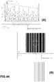
- FIG. 1 shows is a schematic illustration of a beam defection system for providing a display.
- the display is based on the principle of using a stack 1 of electrically switchable gratings SBGs to deflect input light 100 from an image generator 2 into FOV regions or tiles.
- each SBG is essentially a planar grating beam deflector that deflects incident TIR light into output light forming a unique FOV tile.
- the SBG elements 10A-10D provide a first row of four FOV tiles, elements 11A-11D provide a second row of four FOV tiles, and elements 12A-12D provide a third row of four FOV tiles,
- the image light is collimated and may be delivered to the SBG stack by, for example, a light guide or Substrate Guided Optics.
- the substrates used to containing the SBGs may provide the light-guiding substrate.
- Figure 2 shows how a horizontal field of view can be generated using 4 SBGs 10A-10D configured in four separate layers.
- One input SBG is to provide for directing input image light from the image generator into a TIR path.
- the input image generator may comprise a laser module, microdisplay and optics for collimation and beam expansion.
- the output SBGs may be staggered horizontally to provide image continuity in FOV space.
- FIG. 2 shows the limiting rays in one plane for the SBG group 3 corresponding to one row of FOV tiles 10A-10D.
- the limiting rays 101A-101D and the maximum angular extent ⁇ 1 relative to the normal 102, 103 the display are shown.
- the rays define the exit pupil 104.
- each subfield of view is limited by the diffraction efficiency and angular bandwidth of the SBG.
- SBG grating devices may have angular bandwidths in air of approximately ⁇ 5° (subject to material properties, index modulation beam geometry and thickness). In one embodiment, larger angles can be achieved in practice by using thinner SBGs.
- the SBG may have a thickness less than or equal to about 4 ⁇ m - e.g., less than or equal to about 3.5 ⁇ m, 3 ⁇ m, 2.5 ⁇ m, 2 ⁇ m, 1.5 ⁇ m, 1 ⁇ m, 0.5 ⁇ m or smaller.
- the increased bandwidth resulting from thinner SBGs may result in lower peak diffraction efficient. In one embodiment, it may be desired to increase the refractive indeed modulation.
- the top SBG 10A provides a field of view of -20° to -10°; the next SBG 10B provides the field of view-10° to 0°; the next SBG 10C provides the field of view 0° to 10°; the and the lower SBG 10D provides the field of view 10° to 20°; one provides the right 20°.
- Each output put FOV provides a FOV tile of horizontal extent 10 degrees and a vertical extent set by the input collimation optics and the waveguide limitations typically 10 degrees.
- SBGs have a switching speed of as little as, for example, 35 microseconds
- the eye integrates the separate optical outputs, and a 40° horizontal field of view by 10 degree vertical field of view is perceived.
- the input image generator generally indicated by 2 is update with a new digital image.
- the input image generator provides an image of approximately 1000 pixels horizontal by 800 pixels vertical resolution. Hence the complete perceived image has a resolution of 4000x800 pixels.
- the tiles may abut in FOV space through the exit pupil defined by the overlapping light rays from the SBG layers.
- the stacking approach shown in FIG. 1 may be suitable for relatively modest FOV.
- horizontal field of view of around 60 degrees by 10 degree vertical is feasible.
- the number of SBG layers needed becomes impractical: six layers is the current practical limit before the performance of the display is compromised by scatter, absorption, and other optical losses. If additional layers for blue and green are added as schematically indicated by 13, 14, the number of tiles would be increased by x3.
- RGB SBGs One method to avoid using separate RGB SBGs is to use multiplexed SBGs, in which the illumination is provided from opposite ends of the lightguide as R and B/G illumination, compromising the color gamut somewhat.
- multiplexed gratings raise issues of fabrication complexity and cross talk.
- One benefit of the embodiments described herein is minimizing the need for very large numbers of SBG layers.
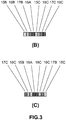
- One embodiment provides compressing the stack by interlacing the SBGs, as shown in FIG. 3 , as opposed to simply stacking the gratings, as illustrated in FIGS. 1-2 .
- FIGS. 1-2 One embodiment provides compressing the stack by interlacing the SBGs, as shown in FIG. 3 , as opposed to simply stacking the gratings, as illustrated in FIGS. 1-2 .
- an apparatus for displaying an image comprising a multiplicity of groups of selectively switchable beam deflecting elements.
- the beam deflectors are SBGs having a first diffracting state and a second diffracting state.
- the first diffracting state may exhibit high diffraction efficiency and the second diffraction state may exhibit low diffraction efficiency.
- the SBGs may operate in reverse mode such that they diffract when a voltage is applied and remain optically passive at all other times.
- the SBGs may be implemented as continuous SBG lamina separated by thin (as thin as 100 microns) substrate layers.
- the substrate may comprise plastic.
- the substrate may comprise plastic substrates with transmissive conductive coatings (instead of ITO).
- each group comprising four elements labelled by the characters A-D.
- the repetition of the pattern of SBG elements is indicated by the dotted line.
- the number of groups of beam deflecting elements or the number of elements per group is not limited.
- the elements are forming in a thin HPDLC grating lamina 15 sandwiched by the transparent substrates 14A, 14B.
- Transparent electrodes are applied to opposing faces of the substrates with at least one of the electrodes being patterned to overlap the SBG elements.
- An input image generator which will be described in more detail later, provides collimated image light generally indicated by 100.
- Each group of beam deflecting elements diffracts image light into a multiplicity of rays providing a set of FOV tiles. Elements corresponding to a given tile will have a unique grating prescription.
- the rays may define an exit pupil according to geometrical optical principles.
- the limiting rays from the group 15 and 18 in the projection of the drawing are indicated by 107, 108.
- Each element has a diffraction efficiency angular bandwidth ⁇ . Comparing FIG. 3 with FIG. 2 , it should be apparent that the embodiment of FIG. 3 is equivalent to interspersing the SBG layers shown in FIG. 2 within a single SBG lamina.
- the first multiplicity of beam deflecting elements and the second multiplicity of beam deflecting elements are uniformly interspersed a shown in FIG. 3B . In one embodiment, the first multiplicity of beam deflecting elements and the second of multiplicity beam deflecting elements are randomly interspersed as shown in FIG. 3C .
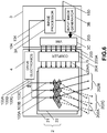
- Fig. 3 shows the principles of an HMD.
- a display based on the above principles may comprise two sub systems: a color waveguide (which herein also refers to a DigiLens) and a device configured to inject an input image into the color waveguide (also referred herein to an Image Injection Node).
- the DigiLens comprises a stack of three separate RGB waveguides each providing a red, green or blue color imaging channel.
- each waveguide is further divided into two holographic layers (to be referred to as a doublet).
- the description will assume double layers unless stated otherwise.
- the DigiLens 2 comprises the doublet further comprising layers 21, 22.
- the apparatus further comprises the IIN 3, DigiLens drive electronics 4, and a coupler for admitting light from the IIN into the DigiLens.
- the IIN and the DigiLens drive electronics are connected by the communication link 103.
- Each SBG layer contains arrays of SBGs comprising sets of sub arrays, where the members of any given sub array have one of a predefined set of optical prescriptions, each prescription corresponding to a unique FOV tile.
- the number of SBG prescriptions equals the number of FOV tiles.
- a prescription defines the Bragg grating geometry needed to deflect incident TIR input light from the IIN into output light that defines a FOV tile.
- the drive electronics provides voltage outputs 103A-103C.
- the connections 104A-104C to the SBG elements 300A-300C is shown.
- FIG. 5 shows input collimated image light 200 from the IIN being coupled into the DigiLens to provide the collimated image light 201 at the input to the waveguide 2.
- Typical collimated output beams from the waveguide for the SBG sub arrays 200-202 are generally indicated by 202A-202C.
- the SBGs operate in reverse mode such that they diffract when a voltage is applied and remain optically passive at all other times.
- the SBGs may be implemented as continuous SBG lamina separated by thin substrate layers (as thin as 100 microns) as shown.
- This is a planar monolithic design harnessing the full assets of narrow band laser illumination with monolithic holographic optics.
- the motivation for configuring the SBGs as monochromatic layers is to enable the use of holographic optics and SBG beam splitter to provide a flat, solid state, precision-aligned display, minimizing the need for bulky refractive optics.
- the resolution of the display is only limited by that of the microdisplay.
- the design is scalable to a larger FOV by interlacing more tiles in each layer and/or adding new layers. Likewise the pupil, eye-relief and FOV aspect ratio can be tailored to suit the application.
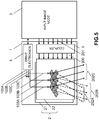
- FIG. 6 shows the IIN in more detail in one embodiment.
- the role of IIN is to form a digital image, collimate it, and inject it into the DigiLens.
- Two separate optical subsystems may be employed: one to illuminate the microdisplay and one to collimate the image.
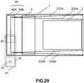
- the IIN may comprise an image processor 3A, input image generator 3B, and a vertical beam expander (VBE) 3C.
- the image processor provides image data to the input image generator via the communication link 150.
- the image processor also controls the switching of the SBG elements in the DigiLens by means of an electronic link to the DigiLens drive electronics.
- the input image generator which will be discussed in more detail in the following description, may comprise a laser module and microdisplay.
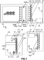
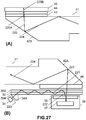
- FIG. 7 illustrates the operation of the IIN in further detail concentrating on the input image generator and the VBE and referring to the XYZ orthogonal coordinate axes provided in the drawings.
- the front elevation view corresponds to the YX plane, and the Y axes refer to the vertical direction as perceived by the viewer of the display.
- the VBE comprises a SBG 60 sandwiched by substrates 61A, 61B.
- Image light from the image generator undergoes TIR, as indicated by 204 within the waveguide formed by the substrates.
- the VBE is designed to be lossy. In other words, the diffraction efficiency of the grating is low at the end nearest the image generator and highest at the furthest extremity.
- One effect is that it couples light, such as 204A, 204B, out towards the couple 5 along its entire length providing a vertical beam expansion (in the Y direction) to match the height of the DigiLens waveguide.
- Image light may be coupled into the VBE by a grating coupler 31A.
- holographic objective 31 and a holographic field lens 32 both optically connected to light guiding device 33.
- Image light from the microdisplay 207 is admitted to the light bide via the holographic objective and follows the TIR path 208 until it is directed out of the light guide into the VBE by the holographic objective 32 as output light 203.
- the light guide 33 includes inclined surfaces at each end.
- the drawing inset 63 shows the configuration of the laser module and microdisplay.
- the illumination of the microdisplay 37 may be performed using a diode laser 34, a waveguide, and a SBG beam splitter.
- the SBG beam splitter may be formed as lamina 36 sandwiched between transparent substrates 35A, 35B forming the waveguide. A slanted SBG grating is recorded in the portion of the lamina 35A overlapping the microdisplay.
- Collimated P-polarised light 210 from the laser module is admitted into the waveguide by a coupler 36.
- the coupler may be a prism. In some embodiments, the coupler may be a grating device.
- the coupled light follows the TIR path 211 up the SBG beam splitter, where according to the properties of SBGs the P-polarised light is diffracted towards the microdisplay. On reflection the light becomes S-polarized and passes through the SBG beam splitter without substantial loss or deviation to emerge from the waveguide as the collimated image light 207.
- the reflective microdisplay could be replaced by a transmissive device.
- an emissive display may be used.
- components such as anamorphic lenses and light shaping diffusing elements may be used in certain applications to control image aspect ration and illumination uniformity.
- the apparatus may further include a despeckler.
- the IIN may comprise, or be, a diffractive optical device.
- the processes carried out by the IIN, as employed in pre-existing techniques, may use several refractive lenses, a polarizing beam splitter cube, and a precision housing for aligning and assembling the various components. Not only are the piece parts expensive, but the touch labor is excessive. In addition, the whole assembly is difficult to ruggedize and, in the end, heavy and bulky. Miniaturized components can reduce size and weight, but they also sharply increase component costs and assembly time.
- the description of the IIN has referred to just one monochromatic microdisplay.
- the IIN optical components would need to be replicated for each color. Since the optical design uses substrate guided optics and diffractive optical elements, the combination of the red green and blue channels in one embodiment can be accomplished within a very compact form factor that is only limited by the size of the microdisplay and laser module and the overall system design needs.
- the interlacing of the SBG elements in the DigiLens may be carried out in many different ways.
- the interlaced gratings in the embodiment of FIG 1 may be configured in the fashion of a Venetian blind (as disclosed in Provisional Patent Application No. 61/627,202 by the present inventors).
- the MTF associated with such geometry has notches in it at spatial frequencies traceable to the periodic nature of the interleaving.
- introducing a complex tessellation of gratings this deficiency can be rectified.
- "Tessellation" in at least some embodiments herein is defined as the process of creating a two-dimensional surface pattern using the repetition of a geometric shape with no overlaps and no gaps.
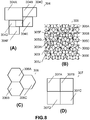
- the tessellation pattern is not limited to diamond shaped tessellation patterns of the type illustrated in FIG. 4-7 . It will be appreciated that patterns based on squares, rectangles, triangles may be used. While a regular patterning is implied in the drawings, it may be advantageous in certain cases to have a randomly distributed pattern. In one embodiment, it may also be possible to use elements of different sizes and geometries in a given pattern. Many possible schemes exist. The elements may have vertically or horizontally biased aspect ratios. In one embodiment, a broader horizontal aspect ratio results in a better horizontal resolution. As will be shown below 1.38 mm. x 0.8 mm, diamonds give acceptable resolution.
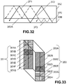
- FIGS. 8-10 show a tiling pattern 304 comprising rectangular shapes 304A-304F having a multiplicity of vertical and horizontal dimensions.
- FIG. 8B shows a tiling pattern 305 known as Penrose tiling comprising elements 305A-305J.
- FIG. 8A shows a tiling pattern 304 comprising rectangular shapes 304A-304F having a multiplicity of vertical and horizontal dimensions.
- FIG. 8B shows a tiling pattern 305 known as Penrose tiling comprising elements 305A-305J.
- FIG. 8C shows a tiling pattern 306 based on regular hexagons comprising elements 306A-306C.
- FIG. 8D shows a tiling pattern 306 based on squares comprising elements 307A-306D.
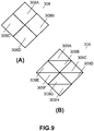
- FIG. 9A shows a tiling pattern 308 based on diamond shapes comprising elements 308A-308D.
- FIG. 9B shows a tiling pattern 309 based on isosceles triangle shapes comprising elements 309A-309D.
- FIG. 10A shows a tiling pattern 310 based on horizontally elongated hexagons comprising elements 310A-310C.
- FIG. 10B shows a tiling pattern 311 based on rectangles with horizontally biased aspect ratios comprising elements 311A-311D.
- FIG. 10C shows a tiling pattern 312 based on rectangles horizontally elongated diamond elements 312A-312D.
- the technology used for fabricating SBG arrays regularly produces features as small as 50 microns (500 dpi), so that interlacing features in the manner described above is not an issue.
- One important condition is that the distance between gratings of like prescription should be small compared to the size of the eye pupil under bright conditions (assumed to be 3 mm in bright sunlight).
- banding is not observable.
- light lost from a band moving beyond the pupil of the eye is offset by light gained from another band moving into the pupil.
- the luminosity variation anticipated from this effect, assuming uniform illumination across the waveguide, is approximately ⁇ 1% of the average brightness level.
- the concept of banding may be most readily understood in embodiments where the SBG elements comprise columns. However, the basic principle may apply to any type of patterning that may be used with any embodiments described herein.
- image light is admitted into one end of the DigiLens only.
- Each waveguide in the DigiLens may generally comprise two SBG layers. It should be apparent from consideration of the drawings and description that in such embodiments the layers may comprise SBG arrays of identical prescription with one reversed and the image injection node being configured in two symmetrical portions to provide separate image light in opposing paths to the two holographic layers. Such embodiments may need duplication of components and are therefore likely more expensive to implement.
- each DigiLens doublet waveguide is 2.8 mm thick.
- the SBG layers may in theory be separated by low index substrates or air gaps.
- the gratings may be 3 microns in thickness sandwiched by substrates of thickness 100-200 microns. The thicknesses of the transparent electrodes applied to opposing faces of the substrates are measured in nanometers.
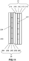
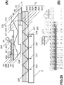
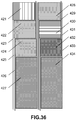
- FIG. 11 is a schematic cross-sectional view of a DigiLens waveguide comprising two layers 20, 21 in one embodiment.
- Layer 20 comprises transparent substrate 20A, transparent patterned electrode layer 20B, SBG array 20C containing elements such as 20F, a transparent electrode layer 20D, and a second substrate 20E.
- Layer 21 comprises transparent substrate 21A, transparent patterned electrode layer 21B, SBG array 21C containing elements such as 21F, a transparent electrode layer 21D, and a second substrate 21E.
- the substrates 20E and 21A may be combined into a single layer.
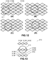
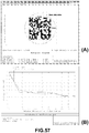
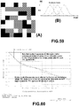
- FIGS. 12A-12D shows examples of tessellation patterns in the regions containing SBG elements of types labelled 1-4.
- the eye pupil 311 is overlaid.
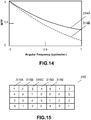
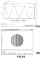
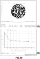
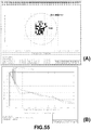
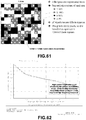
- FIGS. 13-14 shows MTF data for one particular SBG element type configured as shown in FIG. 13 at one eye pupil location in the display exit pupil.
- the SBG elements are labelled by 313A-3131.
- FIG. 14 shows the MTF curves.
- the upper curve 314A is the diffraction limited MTF
- the lower curve is the estimated SBG array MTF allowing for aberrations.
- This architecture is applicable to a 2 layer (1 doublet) monochrome design, or a single color layer in the R, G, B color design. Three stacked doublet layers give the composite performance.
- the exit pupil 311 is 3 mm in diameter in this embodiment.
- the first layer which is illustrated in Figure 13 , tiles all of the horizontal (lower) tiles: L1-4 and the horizontal (middle) tiles (MID,1), (MID,2).
- the second layer tiles the horizontal (middle) tiles: (MID,3), (MID,4), and all of the horizontal (upper) tiles: U1-4.
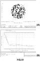
- FIG. 15 shows an example of tiling using rectangular SBGs with horizontally biased aspect ratios.
- the tiling pattern 315 comprises element types 1-5 also labelled by the numerals 315A-315E.
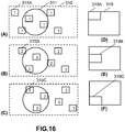
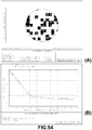
- FIG. 16 illustrates in one embodiment how the DigiLens tiles the FOV in the exit pupil in three consecutive stages of the formation of a monochromatic image.
- the writing of images of each primary color will follow a similar process.
- FIGS. 16A-16C show three types of SBG 1-3 also indicated by the labels 315A-315C being activated.
- the eye pupil 311 and the exit pupil 316 are overlaid in each case.
- the corresponding FOV tiles 319A-319C in FOV space indicated by the rectangle 319 are shown in FIGS 16D-16F . Only a small number of SBG elements are illustrated to simplify the understanding of the switching process. Note that all SBG elements of a given type can all couple light out simultaneously owing to the "lossy" coupling between the beam and grating.
- the diffraction efficiency of individual elements is modulated to extract a fraction of light the light available from the guided beam.
- the first elements the guide beam interacts with have the weakest coupling efficiency, while the elements at the other extremity of the beam path have the strongest.
- the area of the pupil filled by light from SBGs of a given type is roughly fixed. As the eye moves from left to right, light is lost from the leftmost SBG elements, but is gained on the right hand edge.
- the luminosity variation arising from this effect, assuming uniform illumination across all elements, is approximately 2% (+/-1% of the average brightness level).
- the periodicity of the SBG elements could yield unwanted artifacts resulting from diffraction by the element apertures or even interference effects. The latter is believed to be unlikely because light propagating in the planar waveguide structure will not necessarily be in phase with light from the next aperture because of the unequal optical path lengths inherent in planar waveguide structures. Light exiting each periodic aperture is therefore expected to combine incoherently (even if the coherence length of the laser is reasonably long with respect to the planar waveguide structure) when considered across all SBG elements. In the event that an unwanted artifact does arise from the SBG element, periodicity on the proposed strategy would involve randomizing the elements.
- DigiLens Points across the DigiLens aperture contribute angular information to the 10 mm eye box progressively differently because of the 25 mm eye relief. Points towards the left of the display do not contribute angular content from the right of the FOV, and vice versa.
- the DigiLens in one embodiment may be optimized to fill the desired eyebox at the prescribed eye relief.
- Figures 10A-10D indicate the portions of the SBG aperture that contribute to the eyebox in one embodiment.
- the minimum size of the outcoupling SBG is just less than 30 mm wide. However, only a very small region in the center of the DigiLens provides content at all field angles "e.g.: -15° ⁇ 5°, -5° ⁇ 5°, +5° ⁇ 5° and +15° ⁇ 5°. These angular bands correspond to outcoupling SBG columns 1, 2, 3, and 4 (found for each of Upper (+10°), Mid (+0°) and Down (-10°) fields).
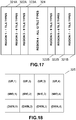
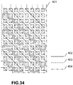
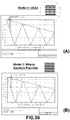
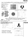
- FIG. 17 shows the distribution of SBG tile types for the 3 vertical x 4 horizontal FOV tiling pattern of FIG. 18 .
- all 12 SBG prescriptions are needed in the centre of the FOV, while the number needed falls to just one at the horizontal limits of the FOV
- FIG. 18 shows an exemplary FOV tiling pattern that may be used to tile a 52° X 30° FOV (assuming each SBG prescription provides 13° x 10°).
- a total of 12 different types of SBG prescriptions need to be provided comprising "UP”, “MIDDLE” and “DOWN” elements for vertical tiling and four horizontal tiling prescriptions for each of the vertical tiling SBGs tiles (labeled 1-4).
- Each type of SBG will be represented by more than one SBG element.
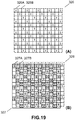
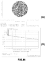
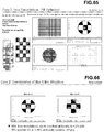
- FIGS. 19-23 illustrate SBG patterns, which correspond to each of the tiling regions defined in FIGS. 17-18 .
- the single layer pattern and two overlaid patterns for on SBG type are illustrated. Square elements have been assumed in this embodiment.
- FIG. 19 shows patterns corresponding to regions 1 and 7 (3 tile types). The two layers are indicated by 326, 327, each layer comprising type 1 elements 326A, 327A and spaces 326B, 327B (to be occupied by elements of other types). In this case, one layer achieves 33% aperture fill and one doublet achieves 66% aperture fill.
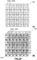
- FIG. 20 shows patterns corresponding to regions 2 and 6 (6 tile types).
- the two layers are indicated by 328, 329, each layer comprising type 1 elements 328A, 329A and spaces 328B, 329B. In this case, one layer achieves 16.7% aperture fill and one doublet achieves 33% aperture fill.
- FIG. 21 shows patterns corresponding to regions 3 and 5 (9 tile types). The two layers are indicated by 330, 331, each layer comprising type 1 elements 330A, 331A and spaces 330B, 331B. In this case, one layer achieves 11.1% aperture fill and one doublet achieves 22.2% aperture fill.
- FIG. 22 shows patterns corresponding to region 4 (12 tile types). The two layers are indicated by 332, 333, each layer comprising type 1 elements 332A, 333A and spaces 332B, 333B. In this case, one layer achieves 8.33% aperture fill and one doublet achieves 16.7% aperture fill.
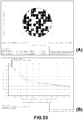
- the resulting composite pattern 340 is shown FIG. 23 .
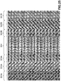
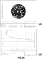
- An example of the coverage of a single SBG type in a three layer waveguide 341 is shown in FIG. 24 .
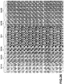
- FIGS 25-26 show SBG patterns for each layer of a two layer waveguide in one embodiment.
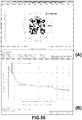
- the eye is photoreceptor limited. Cone spacing at the fovea can be as small as 2.5 ⁇ m, equivalent to 60 cyc/deg. At larger pupil apertures, the eye's performance degrades significantly due to aberration in the eye. At about 3 mm, the eye's performance is close to diffraction limited.
- the eye is therefore photoreceptor density limited in this embodiment.
- the display projection magnification from the microdisplay to the retina is approximately 2.
- the angular size of the microdisplay pixels at the eye is 6.0 ⁇ m giving a display 83 cyc/mm Nyquist frequency at the retina (1.4 cyc/mr).
- Image sharpness may be assessed to be sharp when contrast is maximized (and is high) at the half Nyquist limit (i.e., about 40 cyc/mm in the following plots showing image quality at the retina).
- SBGs are Volume Bragg gratings, and in one embodiment may not support higher orders as would be found with blazed or thin grating. The absence of higher orders may minimize (or even eliminate) ghost images.
- within the waveguide light which continues to be wave guided (in the lossy waveguide) will not 'see' the output apertures of the tiles.
- phase diversity should exist across the output SBG apertures. Polarization diversity will further assist with the despeckling, and hence minimize the effects of any diffractive artifacts from the structure. As a further safeguard, noting that it is not essential to have straight edges on the SBG apertures, the edges will be patterned to randomize any artifacts.
- tessellation limitations to maximize pupil fill.
- the offsets between the SBG patterns in the two layers need not have a non-integer offset to tessellation pattern design in x or y.
- an x offset will in effect cause a half pixel on one side or another of a region, and would then need ITO addressing for half of a pixel in that area alone. In one embodiment, it is better to avoid this to retain a uniform addressing pitch.
- an offset in y of the pattern would similarly need half pixel vertical addressing. Similarly, it would be desirable to avoid this. It is acceptable to have a half pixel offset in y to maximize coverage, but then all patterns need to have half pixel offset in same direction.
- all 12 tile types are employed on each doublet. However, the maximum tile type fill is obtained for 9 tiles types on two layers. We also have cases where 6 tile types and 3 tile types need to be configured, for example, on two layers. Consider, for example, a region where three horizontal tile types to fill eye pupil for a single vertical tile band in one embodiment. Note that other layers of doublets address the other two vertical tile bands. Layers 1 and 2 both contain the same tiles, but in an offset arrangement to achieve the desired pupil filling.
- 1 mm x 1 mm squares have been used to simplify the optical modeling; however, the principles are identical no matter the shape. However, it should be noted that certain shapes will pack preferentially.
- FIGS. 27-29 illustrate some embodiments of the IIN comprising a input image generator comprising the diode laser module 34, coupling prism 34A, SBG beam splitter layer 35 sandwiched between substrates 35A, 35B, microdisplay module 38, light guide 41 contain include surfaces 42A, 42B, input coupling, holographic objective, spacer half wave plate, holographic field lens.
- the IIN provides a telecentric (slightly projected) pupil to allow better coma control and better packaging with the pupil vertical beam expander.
- FIG. 28A is a cross sectional view illustrating the coupling from the Input Image Node to the DigiLens via the VBE in one embodiment.
- FIG.28B shows a detailed ray trace of the emebodiment of FIG.28A .
- the VBE may comprise, or is, a lossy grating extracting light from the beam over a distance corresponding to the height of the DigiLens.
- the light is well ordered in that light across the pupil is arranged in tight field bundles.
- the different numbers of bundles of light with different field angles may cause the bundles to be more distributed.
- the pink ray with the highest waveguide angle may be furthest from the rest of the VBE waveguide.
- the steepest ray in waveguide starts furthest to the left.. This may help keep the passive input coupler (and VBE thickness) down.
- At the far end (fully to the left) coupling out of the VBE into the waveguide is hampered by the loss of order, as found at the input.
- a 50/50 active coupler is used in one embodiment at the VBE to DigiLens coupling stage.
- FIG. 29 is a plan view of the DigiLens and the VBE showing how the latter is split into two switchable elements. This reduces the waveguide thickness.
- Each DigiLens doublet waveguide is 2.8 mm thick. Without the switch, the thickness doubles such that the total waveguide thickness increases from around 10 mm, to about 18 mm.
- Figure 10 shows rays traced from the VBE to the DigiLens.
- Several embodiments provided herein may have to be well suited for substrate guided optics.
- component costs may be reduced.
- the optical complexity is contained in the various holographic optical elements.
- NRE non-recurring engineering
- the replication costs are relatively insignificant, as compared to the recurring material costs associated with discrete refractive components.
- assembly time may be reduced. Not only is part count reduced, but the assembly process is also much faster.
- the planar structures can be cost-effectively laminated together with very high optical precision using alignment fiducials. The touch labor is greatly reduced, as compared to that of building a piece-part assembly to exacting standards.
- the optical precision is greater.
- the desired transmission for the color display is >70%, with an objective of >90%. Assuming three waveguides per display and two substrates per waveguide, the calculated transmission is 93%, meeting the stipulated objective.
- the design described herein may use 100-micron glass substrates.
- the total thickness of the display of the color display may be still less than 1 mm.
- the thicknesses of the holographic layers (including the coatings) are negligible; each contributes only 4-5 microns to the overall thickness. Since weight is always an issue, this may be an important feature of the embodiments described herein. In one embodiment where the substrate comprises plastic, the weight may be further reduced.
- the SBGs operate in reverse mode such that they diffract when a voltage is applied and remain optically passive at all other times.
- the SBGs may be implemented as continuous SBG lamina separated by thin (as thin as 100 micron) substrate layers as shown.
- the design goal is to use plastic substrates with transmissive conductive coatings (to replace ITO).
- Plastic SBG technology suitable for the present application is being developed in a parallel SBIR project. In this embodiment, this is a planar monolithic design harnessing the full assets of narrow band laser illumination with monolithic holographic optics
- Configuring the SBGs as monochromatic layers may enable the use of holographic optics and SBG beam splitter technology to provide a flat solid state precision aligned display totally eliminating the need for bulky refractive optics.
- the resolution of the display is only limited by that of the LCoS panels.
- the design is scalable to a larger FOV by interlacing more tiles in each layer and/or adding new layers.
- the pupil, eye-relief, and FOV aspect ratio can be tailored to suit the application.
- the design can be scaled down to a smaller FOV.
- FIGS. 30A-30B illustrate a scheme for polarization recycling for use with at least some embodiments described herein. This may be relevant in the event that polarization is not maintained with an SBG outcoupling waveguide, either by virtue of the properties of the SBG material (current or one developed in future), or where a polarization rotation component is deliberately introduced in the waveguide.
- a thinner DigiLens waveguide can be used if linearly polarized light is input into the DigiLens waveguide (i.e., light coupled from VBE into the waveguide), and light is converted to a mixture of S and P polarized light. This may allow up to a factor of two times reduction thinness of the waveguide.
- FIG. 30A shows a waveguide 252 with input rays 354A, 354B directed into the TIR paths labelled by 355A, 355B by a coupling grating 353.
- the light may be of any polarization. However, for a SBG input grating P-polarzation may be desirable in one embodiment.
- the coupling grating aperture is A.
- the TIR angle has been chosen to be 45° so that the thickness of the waveguide required for the limiting input ray to just skirt the edge of the coupling grating after the first TIR bounce is A/2.
- the waveguide 356 has input coupling optics comprising the first and second gratings 357A, 357B disposed adjacent each other, the half wave film 357C sandwiched by the waveguide and the first grating; and a polarizing beam splitter (PBS) film 357D sandwiched by the waveguide and the second.
- the PBS is design to transmit P-polarized light and reflect S-polarized light. Again the TIR angle is chosen to be 45° only for illustration purpose.
- Input P-polarized collimated light 358A, 358B is coupled in to the waveguide via the first grating and half wave film (HWF) to provide S-polarized light 359A, and via the second grating and PBS to provide P-polarized light 359C, 359D.
- HWF first grating and half wave film
- the input coupling aperture can be the equal to the length of two TIR bounces owing to the polarization recovery by the HWF and PBS.
- the input couplet cannot be longer than one TIR bounce because grating reciprocity would result in the light being diffracted downwards out of the waveguide.
- the waveguide thickness can be reduced by 50%; that is, for a coupler length equal to A the waveguide thickness (for 45° TIR) is A/4.
- S and P lights in the waveguide are not separated.
- the input light will be divergent resulting in the S and P light quickly becoming spatially mixed.
- the polarization rotation may arise from the reflective characteristics of the waveguide walls and from the birefringence of the holographic material where SBGs are used.
- polarization rotation is provided by applying a quarter wave film (QWF) to the lower face of the waveguide.
- QWFs and QWFs may be about 0.125 mm thick.
- a typical adhesive layer may be about 75 microns.
- the polarization control films do not contribute significantly to the overall waveguide thickness. In certain cases the films can be can be immersed in an adhesive layer used for lamination.
- FIG. 31 illustrates a counter-propagation waveguide for use in some embodiments.
- the waveguide comprises adjacent grating laminas 51A, 51B of identical but opposing prescriptions sandwiched by substrates 52A, 52B.
- Wave guided light 362 propagating from left to right interacts with the grating 51A to provide continuously extracted light 360A-360C to provide the expanded output beam 360.
- Wave guided light 368 propagating from right to left interacts with the grating 51B to provide continuously extracted light 361A-361C to provide the expanded output beam 361.
- FIG. 32 illustrates the use of a beam splitter in a waveguide in one embodiment to achieve uniformity. This principle may be applied both expansion axes.
- a beam splitter offset may be employed in waveguide (i.e., not in middle of waveguiding surfaces, but offset from waveguide midpoint to maximize uniformity following multiple bounce interactions).
- a yet further refinement is to use different reflectivities in beam splitter to optimize and tailor beam mixing. Not to be bound by any particular theory, but by varying the reflectivity % of the beam splitter to something other than 50/50, or by varying the transmission/reflection split along a B/S length, the pupil fill can be homogenized and optimized.
- the waveguide 353 contains a beam splitter layer 352.
- the beam splitter may be provided using a thin film coating.
- a TIR ray such as 370 may then undergo beam splitting, which results in waveguiding occurring between the upper and lower walls of the waveguide; between the upper wall of the waveugid and the beam splitter, and between the beam splitter and the lower wall of the waveguide as indicated by rays 371-373.
- the IIN stop is formed by controlling the profile of the input illumination. In at least some embodiments there is no hard physical stop in the projection optics.
- the benefits of projected stop include decreased waveguide thickness. The stop is projected midway up the VBE to minimize aperture diameter within the VBE, and hence minimizing the aperture width of the VBE to DigiLens waveguide coupler (e.g., reducing the width of the 1 st axis expander) limits the thickness of the 2 nd axis expansion optic.
- FIGS. 33-36 show details of an ITO in some embodiments addressing architecture for use in a DigiLens.
- FIG. 33 shows a method of reducing the number of tracks in a given ITO layer, which method uses dual sided addressing of ITO, and super pixel addressing to reduce the number of tracks by approximately one third.
- the pixels are provide in a first group 35,0 comprising : elements of dimension 3 units x 1 unit such as the ones labelled by 350A, 350B; and elements of dimension 1 unit x 1 unit, such as the ones labelled 350C-350H, and a second overlapping inverted group 351 of identical pixel geometry as indicated by 351A-351G.
- FIGS. 34-36 show how interleaving of electrode wiring tracks may be used to permit a 2D electrode structure to address (switch) multiple different tessellation types.
- FIG. 34 shows a wiring scheme used in embodiment, in which electrode elements such as 401 are connected by tracks 402-404.
- FIG. 35 shows a wiring scheme in another embodiment with electrodes 407-409 and track portions 410,411 indicated.
- FIG. 36 shows the electrodes and tracks of the embodiment of FIG. 33 in more details with the elements and tracks indicated by the numerals 421-434.
- the electrode architecture may benefit in terms of reduction of part complexity from using identical pattern technique, and flip symmetry to create full addressing network. This is not needed to make design work, but may limit number of parts that need to be designed and handled.
- a graduated reflection profile underneath SBG layer is used to control (or assist) with grating DE variation along length (normally achieved in SBG grating using index modulation). This may be useful in cases such as the VBE where low percentage of light is out coupled in the first bounce, but high percentage is coupled out at the other end of the expander.
- 1D expansion engines are used to double input power and/or minimize 1D aperture width.
- the display is configured as a "visor".
- the color waveguide is curved in at least one plane.
- such an embodiment may have a large (30 mm) eye relief and a large exit pupil.
- the large exit pupil may reduce (or even eliminate) the need for IPD adjustment.
- FIG. 37A-37B are schematic plan and side elevation views of a curved visor comprising a DigiLens 71 and optical-electronic modules 70A, 70B to either sides.
- One module will comprise the IIN.
- the second module may contain auxiliary optics and electronics.
- FIG. 38 shows the DigiLens of a curved visor in one embodiment in more detail.
- the DigiLens may comprise laminated waveguides, each containing SBG arrays 73A-73C.
- the three SBG layers are isolated from each other by the cladding layers 72A-72D.
- the ray paths are indicated by 381A-381C.
- the SBG layers are stacked without cladding layers to form a single waveguiding structure.
- the ray paths are indicated by 382A-382C.
- a visor DigiLens is shaped facetted planar elements 76A, 76B allowing the waveguides to be planar.
- gratings 77A, 77B are provided at the optical interfaces 77 between the facets to control the beam angles to ensure efficient coupling of guided image light to the SBG array elements.
- the gratings 77A, 77B may be Bragg gratings.
- a facetted DigiLens comprising planar facets, such as 76A, 76B, is embedded with a curved lightguide 79.
- the embodiments may rely on monochromatic waveguides. However it should be apparent from consideration of the description that in alternative embodiments the waveguides could operate on more than color. Such embodiments may involve a more complicated IIN design.
- the multilayer architectures described herein may not be used with conventional holograms, because they would interfere with each other.
- SBG which can be switched clear to allow time-domain integration of the field of view, may be employed to overcome this challenge.
- One embodiment described herein is related to a HMD, such as one with the following specification:
- One important feature of at least some of the embodiments described herein is that they provide the benefit of see-through.
- the latter is of great importance in Head Up Displays for automobile, aviation and other transport applications; private see-through displays such for security sensitive applications; architectural interior signage and many other applications.
- a holographic brightness enhancing film, or other narrow band reflector affixed to one side of the display the purpose of which is to reflect the display illumination wavelength light only
- the see-through display can be made invisible (and hence secure) in the opposite direction of view.
- the reflected display illumination may be effectively mirrored and therefore blocked in one direction, making it desirable for transparent desktop display applications in customer or personal interview settings common in bank or financial services settings.
- any of the embodiments above describe wearable displays, it will be clear that in any of the above embodiments the eye lens and retina may be replaced by any type of imaging lens and a screen. Any of the above described embodiments may be used in either directly viewed or virtual image displays. Possible applications range from miniature displays, such as those used in viewfinders, to large area public information displays. The above described embodiments may be used in applications where a transparent display is desired. For example, some embodiments may be employed in applications where the displayed imagery is superimposed on a background scene such as heads up displays and teleprompters. Some embodiments may be used to provide a display device that is located at or near to an internal image plane of an optical system.
- any of the above described embodiments may be used to provide a symbolic data display for a camera viewfinder in which symbol data is projected at an intermediate image plane and then magnified by a viewfinder eyepiece.
- One embodiment may be applied in biocular or monocular displays.
- Another embodiment may also be used in a stereoscopic wearable display.
- Some embodiments may be used in a rear projection television.
- One embodiment may be applied in avionic, industrial and medical displays. There are applications in entertainment, simulation, virtual reality, training systems and sport.
- any of the above-described embodiments using laser illumination may incorporate a despeckler device for eliminating laser speckle disposed at any point in the illumination path from the laser path to the eyeglass.
- the despeckler is an electro-optic device.
- the despeckler is based on a HPDLC device.
- Tessellation is a pattern of repeating shapes that fit together without gaps. Use of the term 'tessellation' may refer to a single element of a tessellation pattern. In the practical application of tessellations pertaining to DigiLensTM devices tessellation also means the creation of patterns without substantial gaps between tessellation elements-i.e., where there is high overall aperture fill factor.
- a tessellation element is a region (aperture) of diffraction grating or diffraction gratings, which may be a switchable diffraction grating (SBG).
- SBG switchable diffraction grating
- the tessellation will diffract light over all regions of the tessellation at the same time.
- the diffraction grating may be switchable or non-switchable.
- Micro-Tessellation this is a small tessellation that exists within a larger primary tessellation element.
- the microtessellations within a primary tessellation may have different grating prescriptions.
- Micro-tessellation elements that exist within a primary tessellation element all diffract at the same time. The performance of tessellations and their impact on MTF has been described in earlier documents, wherein a single grating was written into the tessellation.
- Performance considerations of interest are: MTF (resolution) and uniformity of field angles.
- a single field of view will exist in the waveguide. At any given moment in time, this will carry field of view information for a portion of the overall field of view. In the case of an eye display, this is a portion of the projected field that is out coupled from the SGO.
- the out-coupling gratings need to out-couple this field of view content such that the eye can see this field of view information across the eye box, desirably with the same flux entering the eye for each field angle and for all field angles at any position of the eye pupil within the eyebox. From earlier work it is recognized that larger tessellations yield superior MTF (resolution) performance, and field of view irradiance on the eye's pupil is more uniform with smaller tessellations.
- a minimum tessellation size to yield sufficient resolution is dependent on the system resolution sought. However, a minimum tessellation aperture size of 0.5 mm to 1 mm width (or diameter) will approximately be needed to support 0.7 to 1.4 lp/mr resolutions, with larger apertures being preferred in one embodiment. This particularly affects high spatial frequency performance.
- a tessellation is a region of the out-coupling grating that, when in a diffracting state, will diffractively out-couple the light at all points in that tessellation aperture region at the same time.
- the regions within a tessellation may contain with one grating prescription or a plurality of grating prescriptions. This plurality of grating prescriptions may be achieved either by multiplexing the gratings (grating prescriptions share the same area of the tessellation), or by having spatially discrete regions of the tessellation into which is written a single grating only.
- a microtessellation is small tessellation that is switched at the same time as other small tessellation areas. The case of spatially discrete micro-tessellations ( ⁇ T) is examined following.
- ⁇ T gratings may be designed to have angular bandwidth overlap with the neighboring ⁇ Ts (in angular field).
- Modeling micro-tessellations for a given field angle in one embodiment is described below.
- One case to consider is FoV overlap of micro-tessellations causing different field angles to be output at different points.
- Another case to consider is equal irradiance of eye pupil from multiple micro-tessellations for a given field angle. Some field angles would output light equally from multiple micro-tessellations, thereby providing the same irradiance of the eye pupil. It is assumed that some micro-tessellations would then provide less, or no, irradiance of the eye pupil. A top hat model would be appropriate to model this case.
- FIG. 42A A typical angular distribution is shown in FIG. 42A .
- the corresponding spatial distribution is shown in FIG. 42B .
- Case A a top hat function for this field angle gives 50% aperture fill.
- Case B the tiles have different weighting. Aperture therefore is not a top hat function.
- micro tessellations do not need to be square or in the order as shown and may have any shape or order, such as a 2D distribution.
- FIG. 43 illustrates MTF curves ( FIG. 43A ) and a 3D layout drawing FIG. 43B showing the effects of 50% aperture fill: 50 um apertures on a 100 um pitch, 3 mm eye pupil. It was assumed 10 um apertures on 40 um pitch (25% fill factor) and green light (532 nm) only. Note the high modulation in the resulting frequency space.
- FIG. 44 shows the effects of 25% aperture fill: 10 um apertures on 40 um pitch, 3 mm eye pupil. MTF and 3D layout plots are provided. 10 um apertures on 40 um pitch (25% fill factor). Green (532 nm) are assumed.
- FIG. 45 shows the effects 50% aperture fill: 125 um apertures on 250 um pitch, 3 mm eye pupil using a MTF plot ( FIG.
- FIG. 45A 125 um stripe apertures on 250 um pitch (50% fill factor) and Green (532 nm) are assumed.
- the non-randomized, regular periodic structures exhibit dips in the MTF through out the angular frequency range of interest, typically: 1.4 cyc/mr.
- Random Micro-Tessellation Patterns were considered next. Results from periodic aperture functions show 'holes' in the MTF. The following investigates randomization of the eye pupil fill using micro tessellations. Tessellation % fill of 25%, 50% and 75% are considered. For this initial analysis, the tessellation was considered to be 100% of the eye pupil. Later cases consider a 1 mm square tessellation that contains micro tessellations with a 3 mm eye pupil.
- FIG. 46A is a footprint diagram showing the effect of 75% aperture fill of 50 um micro tessellations in 3 mm eye pupil.
- FIG. 46B is a MTF plot showing the effect of 75% aperture fill of 50 um micro tessellations in 3 mm eye pupil
- FIG. 47A is a footprint diagram showing the effect of 50% aperture fill of 50 um micro tessellations in 3 mm eye pupil
- FIG. 47B is a MTF plot showing the effect of 50% aperture fill of 50 um micro tessellations in 3 mm eye pupil
- FIG. 48A is a footprint diagram showing the effect of 25% aperture fill of 50 um micro tessellations in 3 mm eye pupil
- FIG. 48B is a MTF plot showing the effect of 25% aperture fill of 50 um micro tessellations in 3 mm eye pupil.
- FIG. 49A is a footprint diagram showing the effect of 75% Aperture Fill of 125 um micro tessellations 3 mm Eye Pupil.
- FIG. 49B is a footprint diagram showing the effect of 75% Aperture Fill of 125 um micro tessellations 3 mm Eye Pupil.
- FIG. 50A is a footprint diagram showing the effect of 50% Aperture Fill of 125 um micro tessellations 3 mm Eye Pupil.
- FIG. 50B is a MTF plot showing the effect of 50% Aperture Fill of 125 um micro tessellations 3 mm Eye Pupil.
- FIG. 51A is a footprint diagram showing the effect of 25% Aperture Fill of 125 um micro tessellations 3 mm Eye Pupil.
- FIG. 51B is a MTF plot showing the effect of 25% Aperture Fill of 125 um micro tessellations 3 mm Eye Pupil.
- FIG. 52A is a footprint diagram showing the effect of 75% Aperture Fill of 250 um micro tessellations 3 mm Eye Pupil.
- FIG. 52B is a footprint diagram showing the effect of 75% Aperture Fill of 250 um micro tessellations 3 mm Eye Pupil.
- FIG. 53A is a footprint diagram showing the effect of 50% Aperture Fill of 250 um micro tessellations 3 mm Eye Pupil.
- FIG. 53B is a MTF plot showing the effect of 50% Aperture Fill of 250 um micro tessellations 3 mm Eye Pupil.
- FIG. 54A is a footprint diagram showing the effect of 25% Aperture Fill of 250 um micro tessellations 3 mm Eye Pupil.
- FIG. 54B is a MTF plot showing the effect of 25% Aperture Fill of 250 um micro tessellations 3 mm Eye Pupil.
- FIG. 55A is a footprint diagram showing the effect of 1 mm tessellation with 50% fill of 125 um micro tessellations using 3 mm Eye Pupil Diameter.
- FIG. 55B is a MTF plot showing the effect of 1 mm tessellation with 50% fill of 125 um micro tessellations using 3 mm Eye Pupil Diameter.
- FIG. 56A is a footprint diagram showing the effect of 1.5 mm tessellation with 50% fill of 125 um micro tessellations using 3 mm eye pupil diameter.
- FIG. 56B is a footprint diagram showing the effect of 1 mm tessellation with 50% fill of 125 um micro tessellations using 3 mm eye pupil diameter.
- FIG. 55A is a footprint diagram showing the effect of 1.5 mm tessellation with 50% fill of 125 um micro tessellations using 3 mm eye pupil diameter.
- FIG. 56B is a footprint diagram showing the effect of 1 mm tessellation with 50% fill of 125 um micro tessellations using 3 mm eye
- FIG. 57A is a footprint diagram showing the effect of 1 mm tessellation with 50% fill of 125 um micro tessellations using 3 mm eye pupil diameter.
- FIG. 57B is a MTF Plot showing the effect of 1 mm tessellation with 50% fill of 125 um micro tessellations using 3 mm eye pupil diameter.
- the first step is checking the model validity: change from UDAs to Bitmap Greyscale Transmission Apertures. Horizontal strips over 1.5 mm aperture (125 ⁇ m ⁇ Ts) in 3 mm diameter eye pupil.
- FIG. 58A shows a MTF plot of a UDA.
- FIG. 58B shows a Bitmap Aperture Function.
- FIG. 59 shows 1.0 mm tessellation using 125 um micro tessellations randomly positioned with variable transmission and 3 mm eye pupil. Using a variable aperture transmissions improves the model to better represent non-top hat model cases (which are the majority of tessellations). DE values of 0%, 50% and 100% are equivalent to the field angle case shown in FIG. 59A .
- FIG. 60 is a MTF plot showing the effect of 1.0 mm tessellation using 125 um ⁇ Ts randomly positioned with variable transmission and a 3 mm eye pupil. Note that spatial frequencies in the upper boxed region fall in between prediction shown in the figures relating to top hat predictions for 125 um pixels with 50% and 75% aperture fill). Higher spatial frequencies shown in the lower boxed region are most affected by the primary tessellation shape. The reader is referred to the figures showing for 50% aperture fill. It should also be noted that there is MTF improvement for 75% aperture fill.
- FIG. 61 a 1.5 mm tessellation using 125 um micro tessellations randomly positioned with variable transmission and 3 mm eye pupil was considered.
- Four different tile types are represented in FIG. 61 .
- the transmission values of each were: 50%; 100%; 50%; 0%.
- the micro tessellations apertures were 125 um squares.
- the grid is 12x12 pixels, so the tessellation aperture is 1.5 mm x 1.5 mm square.
- FIG. 62 is a MTF showing the effect of 1.5 mm tessellation using 125 um micro tessellations randomly positioned with variable transmission and 3 mm eye pupil. It should be noted that high spatial frequencies most affected by the primary tessellation shape, so increasing underlying tessellation from 1.0 mm to 1.5 mm improved high frequency response.
- micro-tessellation structures with spatial randomization across a tessellation provides additional design flexibility.
- tessellation angular bandwidth (ABW) is enhanced at the expense of MTF.
- Results show that Randomization of micro tessellation features permits homogenization (roughly an averaging) of MTF oscillations found in non-randomized patterns.
- MTF at spatial frequencies that are of less interest can be sacrificed for improved tessellation ABW.
- Different cases of relevant overlapping gratings need to be considered.
- the MTF supported by micro-tessellation is dependent on micro-tessellation size and overlapping %.
- the ABW of representative cases of overlapping tessellations need to be considered in more detail, in conjunction with the fold gratings desired to support the desired architecture.
- Micro-tessellations with feature sizes of 50 ⁇ m, 125 ⁇ m and 250 ⁇ m have been considered in the context of a 3 mm eye pupil and 0.5 mm, 1.0 mm and ⁇ 3 mm sized primarily tessellation elements. These are practical numbers to work with in the context of a near eye display. Tessellations may however be any size or shape, and micro-tessellation may be any size or shape smaller than the primary tessellation.
- FIG. 63 Case 1, which comprises 1 mm tessellations, was considered.
- FIG. 63 represents 6 layer, 12 tile, monochrome reference design. It was assumed a single tile with 50% Aperture Fill. It was further assumed: 17 mm eye relief; 3 mm eye pupil; 6 layer monochrome reference design; 1 mm tessellations, and an offset reference design.
- the unit cell is 2x3.
- FIG. 64 shows Case 1b repeated on axis for a 3 mm eye pupil at 30 mm eye relief.
- Eye relief impacts the spatial frequency of the variation.
- the larger eye relief causes higher spatial frequency ripple.
- Uniformity magnitude is unaffected.
- the maximum ripple is 56.6% of pupil fill.
- Minimum ripple is 43.4% of pupil fill.
- Uniformity is +/-13.2%, 26.4% peak-to-peak.
- FIG. 65 shows Case 2: 1 mm tessellations ; fill optimized.
- the Figures represent a 6 layer, 12 tile monochrome reference design with grating positions reoptimized. A single tile has 50% aperture fill. A 3 mm eye pupil and 1 mm tessellations were assumed. The tessellations are spatially uniform.
- FIG. 66 illustrates Case 2: consideration of maximum and minimum situations. Footprint diagrams corresponding to a minimum 45.1% and a maximum 54.9% are shown. With 1 mm tessellations, minimum to maximum best uniformity is +/-5% with 50% aperture fill,i.e., +/-10% uniformity variation (20%p-p).
- FIG. 67 illustrates Case 3: 0.5 mm tessellations with 50% aperture fill, off axis.
- FIG. 67 represents a 6 layer, 12 tile, monochrome reference design but with 0.5 mm tessellations. A single tile: 50% aperture fill and 3 mm eye pupil are assumed. This calculation simulates 50% aperture fill with 0.5 mm wide tessellations.
- FIG. 68 illustrates Case 3b: 0.5 mm tessellations with 50% aperture fill, on axis.
- FIG. 68 represents a 6 layer, 12 tile, monochrome reference design but with 0.5 mm tessellations. A single tile: 50% aperture fill; and 3 mm eye pupil were assumed. This simulates 50% aperture fill with 0.5 mm wide tessellations.
- Ripple frequency is ⁇ 1 cycle for 1.25deg.
- FIG. 70 illustrates a 3 mm eye pupil, 33% aperture fill (3 layers, 9 tile types).
- FIG. 70 represents 3 layer, 9 tile, monochrome reference design but with 0.5 mm tessellations. A single tile: 33% Aperture Fill; and a 3 mm eye pupil were assumed.
- FIG. 71 illustrates a 4 mm eye pupil, 33% aperture fill (3 layers, 9 tile types).
- the ripple frequency is ⁇ 1 cycle for 5deg.
- FIG. 72 illustrates a 3 mm eye pupil, 33% aperture fill (3 layers, 9 tile types).
- FIG. 73 illustrates how a unit cell forms an evenly distributed pattern.
- FIG. 74 is a recalculation of the embodiment using a 4 mm eye pupil, 33% aperture fill (3 layers, 9 tile types). This needs the pattern to have 1x3 unit cell, with even columns offset by 0.5 pixel.
- ripple maximum 35.0%
- ripple minimum 31.0%
- FIG. 75 illustrates a 4 mm eye pupil, 33% aperture fill (3 layers, 9 tile types). This embodiment needs the pattern to have 1x3 unit cell, with even columns offset by 0.5 pixel.
- Achieving 50% aperture fill of a single tile provides significantly improved uniformity over even 33% aperture fill ( ⁇ 5x uniformity improvement on 3 mm eye pupil).
- 50% aperture fill 0.5 mm performs significantly better than a 1 mm tessellation: 3% vs. 20% for a 3 mm eye pupil.
- 50% aperture fill for 9 tiles need '4.5' (i.e., 5 layers).
- Eye pupil irradiance uniformity with field angle improves with decreased primary tessellation element size and increase primary tessellation element aperture fill. It is noted that decreased tile type density on a given layer will then improve the irradiance uniformity with field angle because fewer tile types will increase the aperture fill of any single primary tessellation element type. Decreased primary tessellation element size degrades MTF (resolution). It is noted that decreased primary tessellation element size, and increased density of a primary tessellation element type permits irregular patterns. This in turn permits homogenization of MTF of primary tessellations, and the opportunity to vary the irradiance uniformity field angular ripple frequency. The use of small (micro tessellations) inside the aperture of a primary tessellation may improve the overall angular bandwidth of a primary tessellation element, thereby presenting the opportunity to reduce the number of primary tessellation element types desired.
- inventive embodiments are presented by way of example only and that, within the scope of the appended claims and equivalents thereto, inventive embodiments may be practiced otherwise than as specifically described and claimed.
- inventive embodiments of the present disclosure are directed to each individual feature, system, article, material, kit, and/or method described herein.
- the technology described herein may be embodied as a method, of which at least one example has been provided.
- the acts performed as part of the method may be ordered in any suitable way. Accordingly, embodiments may be constructed in which acts are performed in an order different than illustrated, which may include performing some acts simultaneously, even though shown as sequential acts in illustrative embodiments.
- substantially and “about” used throughout this Specification are used to describe and account for small fluctuations. For example, they can refer to less than or equal to ⁇ 5%, such as less than or equal to ⁇ 2%, such as less than or equal to ⁇ 1%, such as less than or equal to ⁇ 0.5%, such as less than or equal to ⁇ 0.2%, such as less than or equal to ⁇ 0.1%, such as less than or equal to ⁇ 0.05%.
- a reference to "A and/or B", when used in conjunction with open-ended language such as “comprising” can refer, in one embodiment, to A only (optionally including elements other than B); in another embodiment, to B only (optionally including elements other than A); in yet another embodiment, to both A and B (optionally including other elements); etc.
- the phrase "at least one,” in reference to a list of one or more elements, should be understood to mean at least one element selected from any one or more of the elements in the list of elements, but not necessarily including at least one of each and every element specifically listed within the list of elements and not excluding any combinations of elements in the list of elements.
- This definition also allows that elements may optionally be present other than the elements specifically identified within the list of elements to which the phrase "at least one" refers, whether related or unrelated to those elements specifically identified.
- At least one of A and B can refer, in one embodiment, to at least one, optionally including more than one, A, with no B present (and optionally including elements other than B); in another embodiment, to at least one, optionally including more than one, B, with no A present (and optionally including elements other than A); in yet another embodiment, to at least one, optionally including more than one, A, and at least one, optionally including more than one, B (and optionally including other elements); etc.
Claims (15)
- Appareil d'affichage d'une image, comprenant :un noeud d'image d'entrée (3) configuré pour fournir au moins une première et une seconde lumière modulée par l'image ; etun dispositif guide d'onde holographique (2) configuré pour propager au moins l'une des première et seconde lumières modulées par l'image dans au moins une première direction, le dispositif guide d'onde holographique (2) comprenant :des pluralités dispersées d'éléments de réseau de Bragg commutables, comprenant au moins une première pluralité d'éléments de réseau de Bragg commutables et une seconde pluralité d'éléments de réseau de Bragg disposés dans au moins une couche (21, 22), la première pluralité d'éléments de réseau de Bragg commutables et la seconde pluralité d'éléments de réseau de Bragg commutables ayant respectivement une première et une seconde géométrie de réseau de Bragg, chaque pluralité d'éléments de réseau de Bragg commutables ayant une géométrie de réseau de Bragg correspondant à un champ unique de région de vision ;dans lequel les première et seconde lumières modulées par l'image sont modulées respectivement avec un premier champ d'informations d'image de vision et un second champ d'informations d'image de vision ;dans lequel la première pluralité d'éléments de réseau de Bragg commutables est configurée pour dévier par diffraction la première lumière modulée par l'image hors de la au moins une couche (21, 22) en une première pluralité de rayons de sortie formant un premier champ de région de vision et la seconde pluralité d'éléments de réseau de Bragg commutables pour dévier par diffraction la seconde lumière modulée par l'image hors de la couche (21, 22) en une seconde pluralité de rayons de sortie formant un second champ de région de vision,caractérisé en ce que,dans la au moins une couche (21, 22), les pluralités dispersées d'éléments de réseau de Bragg ont un nombre entier N1 de géométries de réseau de Bragg différentes dispersées dans une première bande, aboutées vers la gauche et la droite, en séquence, par bandes contenant des éléments d'un nombre entier N2 de géométries de réseau de Bragg différentes où N1>N2, d'un nombre entier N3 de géométries de réseau de Bragg différentes où N2>N3 et d'un nombre entier N4 de géométries de réseau de Bragg différentes où N3>N4.
- Appareil selon la revendication 1, dans lequel la première pluralité d'éléments de réseau et la seconde pluralité d'éléments de réseau forment une mosaïque dans un motif prédéterminé.
- Appareil selon la revendication 1 ou 2, dans lequel la première pluralité d'éléments de réseau et la seconde pluralité d'éléments de réseau forment une mosaïque dans un motif prédéterminé et le motif prédéterminé est au moins l'un d'un motif périodique, d'un motif non périodique, d'un motif semblable et d'un motif à distribution aléatoire.
- Appareil selon les revendications 1, 2 ou 3, dans lequel tous les éléments de la première pluralité d'éléments de réseau ou de la seconde pluralité d'éléments de réseau sont configurés pour être commutés dans un état de diffraction simultanément.
- Appareil selon les revendications 1, 2 ou 3, dans lequel au moins l'une de la première pluralité d'éléments de réseau et de la seconde pluralité d'éléments de réseau a une forme qui comprend au moins l'une parmi celle d'un carré, d'un triangle et d'un losange ;
dans lequel les éléments de la première pluralité d'éléments de réseau ont une première géométrie et les éléments de la seconde pluralité d'éléments de réseau ont une seconde géométrie. - Appareil selon les revendications 1, 2 ou 3, dans lequel au moins l'un de la première pluralité d'éléments de réseau et de la seconde pluralité d'éléments de réseau dans la au moins une couche (21, 22) est optimisé pour au moins deux longueurs d'onde ou dans lequel tous les éléments de réseau sont optimisés pour une seule longueur d'onde dans la au moins une couche (21, 22).
- Appareil selon les revendications 1, 2 ou 3, dans lequel au moins l'un de la première pluralité d'éléments de réseau et de la seconde pluralité d'éléments de réseau a des géométries de réseau de Bragg multiplexées optimisées pour au moins deux longueurs d'onde différentes.
- Appareil selon les revendications 1, 2 ou 3, dans lequel au moins l'un de la première pluralité d'éléments de réseau et de la seconde pluralité d'éléments de réseau a des géométries de réseau de Bragg multiplexées optimisées pour au moins deux largeurs de bande angulaires de rendement de diffraction différent.
- Dispositif comprenant l'appareil selon les revendications 1, 2 ou 3, dans lequel le dispositif est une partie d'un affichage stéréoscopique dans lequel la première et la seconde lumière modulée par l'image fournissent des vues en perspective de l'oeil gauche et de l'oeil droit.
- Dispositif comprenant l'appareil selon les revendications 1, 2 ou 3, dans lequel le dispositif est une partie d'au moins l'une parmi HMD, HUD et HDD.
- Appareil selon les revendications 1, 2 ou 3, dans lequel au moins l'un de la première pluralité d'éléments de réseau et de la seconde pluralité d'éléments de réseau a un rendement de diffraction qui est spatialement dépendant.
- Appareil selon les revendications 1, 2 ou 3, dans lequel la lumière modulée par l'image du au moins un élément de réseau d'une géométrie donnée de réseau de Bragg est présente dans une région de pupille de sortie (104) délimitée par l'ouverture instantanée de la pupille de l'oeil humain (311).
- Appareil selon la revendication 1, dans lequel au moins l'un de la première pluralité d'éléments de réseau et de la seconde pluralité d'éléments de réseau est commutable électriquement.
- Procédé d'affichage d'une image, le procédé comprenant :(i) la fourniture d'un appareil comprenant un noeud d'image d'entrée (3) et un dispositif guide d'onde holographique (2) comprenant au moins une couche (21, 22), dans lequel, dans la au moins une couche (21, 22), des pluralités dispersées d'éléments de réseau de Bragg commutables ont un nombre entier N1 de géométries de réseau de Bragg différentes dispersées dans une première bande, aboutées vers la gauche et la droite, en séquence, par bandes contenant des éléments d'un nombre entier N2 de géométries de réseau de Bragg différentes où N1>N2, d'un nombre entier N3 de géométries de réseau de Bragg différentes où N2>N3 et d'un nombre entier N4 de géométries de réseau de Bragg différentes où N3>N4, les pluralités dispersées d'éléments de réseau de Bragg commutables comprenant un réseau MxN d'éléments de réseau de Bragg commutables, où M et N sont des nombres entiers ;(ii) la génération de lumière modulée par l'image (I, J) par un noeud d'image d'entrée (3) correspondant au champ de région de vision (I, J) pour 1≤I≤N et 1≤J≤M où I et J sont des nombres entiers ;(iii) la commutation d'éléments de réseau de Bragg commutables ayant une géométrie de réseau de Bragg correspondant à un champ de région de vision (I, J) à leurs états de diffraction ;(iv) l'éclairage d'éléments de réseau de Bragg commutables ayant une géométrie de réseau de Bragg correspondant à un champ de région de vision (I, J) avec de la lumière modulée par l'image (I, J) ; et(v) la diffraction de la lumière modulée par l'image (I, J) en champ de région de vision (I, J).
- Procédé selon la revendication 14, comprenant en outre la répétition des étapes (ii)-(v) jusqu'à obtenir un champ de vision complet.
Applications Claiming Priority (3)
| Application Number | Priority Date | Filing Date | Title |
|---|---|---|---|
| US201261687436P | 2012-04-25 | 2012-04-25 | |
| US201261689907P | 2012-06-15 | 2012-06-15 | |
| PCT/US2013/038070 WO2013163347A1 (fr) | 2012-04-25 | 2013-04-24 | Affichage grand angle holographique |
Publications (3)
| Publication Number | Publication Date |
|---|---|
| EP2842003A1 EP2842003A1 (fr) | 2015-03-04 |
| EP2842003A4 EP2842003A4 (fr) | 2016-03-16 |
| EP2842003B1 true EP2842003B1 (fr) | 2019-02-27 |
Family
ID=49483870
Family Applications (1)
| Application Number | Title | Priority Date | Filing Date |
|---|---|---|---|
| EP13765610.4A Active EP2842003B1 (fr) | 2012-04-25 | 2013-04-24 | Affichage grand angle holographique |
Country Status (5)
| Country | Link |
|---|---|
| US (4) | US9341846B2 (fr) |
| EP (1) | EP2842003B1 (fr) |
| JP (1) | JP6238965B2 (fr) |
| CN (2) | CN106125308B (fr) |
| WO (1) | WO2013163347A1 (fr) |
Cited By (16)
| Publication number | Priority date | Publication date | Assignee | Title |
|---|---|---|---|---|
| US11106048B2 (en) | 2014-08-08 | 2021-08-31 | Digilens Inc. | Waveguide laser illuminator incorporating a despeckler |
| WO2022037844A1 (fr) | 2020-08-18 | 2022-02-24 | Bayerische Motoren Werke Aktiengesellschaft | Ensemble affichage à guide d'ondes pour un dispositif d'affichage tête haute 3d dans un véhicule et son procédé de fonctionnement |
| US11281013B2 (en) | 2015-10-05 | 2022-03-22 | Digilens Inc. | Apparatus for providing waveguide displays with two-dimensional pupil expansion |
| US11320571B2 (en) | 2012-11-16 | 2022-05-03 | Rockwell Collins, Inc. | Transparent waveguide display providing upper and lower fields of view with uniform light extraction |
| US11442222B2 (en) | 2019-08-29 | 2022-09-13 | Digilens Inc. | Evacuated gratings and methods of manufacturing |
| US11448937B2 (en) | 2012-11-16 | 2022-09-20 | Digilens Inc. | Transparent waveguide display for tiling a display having plural optical powers using overlapping and offset FOV tiles |
| US11487131B2 (en) | 2011-04-07 | 2022-11-01 | Digilens Inc. | Laser despeckler based on angular diversity |
| US11543594B2 (en) | 2019-02-15 | 2023-01-03 | Digilens Inc. | Methods and apparatuses for providing a holographic waveguide display using integrated gratings |
| US11561409B2 (en) | 2007-07-26 | 2023-01-24 | Digilens Inc. | Laser illumination device |
| US11586046B2 (en) | 2017-01-05 | 2023-02-21 | Digilens Inc. | Wearable heads up displays |
| US11681143B2 (en) | 2019-07-29 | 2023-06-20 | Digilens Inc. | Methods and apparatus for multiplying the image resolution and field-of-view of a pixelated display |
| US11703645B2 (en) | 2015-02-12 | 2023-07-18 | Digilens Inc. | Waveguide grating device |
| US11726323B2 (en) | 2014-09-19 | 2023-08-15 | Digilens Inc. | Method and apparatus for generating input images for holographic waveguide displays |
| US11726332B2 (en) | 2009-04-27 | 2023-08-15 | Digilens Inc. | Diffractive projection apparatus |
| US11726329B2 (en) | 2015-01-12 | 2023-08-15 | Digilens Inc. | Environmentally isolated waveguide display |
| US11747568B2 (en) | 2019-06-07 | 2023-09-05 | Digilens Inc. | Waveguides incorporating transmissive and reflective gratings and related methods of manufacturing |
Families Citing this family (269)
| Publication number | Priority date | Publication date | Assignee | Title |
|---|---|---|---|---|
| GB0522968D0 (en) | 2005-11-11 | 2005-12-21 | Popovich Milan M | Holographic illumination device |
| US9335604B2 (en) | 2013-12-11 | 2016-05-10 | Milan Momcilo Popovich | Holographic waveguide display |
| US9341846B2 (en) | 2012-04-25 | 2016-05-17 | Rockwell Collins Inc. | Holographic wide angle display |
| US11300795B1 (en) | 2009-09-30 | 2022-04-12 | Digilens Inc. | Systems for and methods of using fold gratings coordinated with output couplers for dual axis expansion |
| US10795160B1 (en) | 2014-09-25 | 2020-10-06 | Rockwell Collins, Inc. | Systems for and methods of using fold gratings for dual axis expansion |
| US8233204B1 (en) | 2009-09-30 | 2012-07-31 | Rockwell Collins, Inc. | Optical displays |
| US20200057353A1 (en) | 2009-10-09 | 2020-02-20 | Digilens Inc. | Compact Edge Illuminated Diffractive Display |
| US11204540B2 (en) | 2009-10-09 | 2021-12-21 | Digilens Inc. | Diffractive waveguide providing a retinal image |
| US8659826B1 (en) | 2010-02-04 | 2014-02-25 | Rockwell Collins, Inc. | Worn display system and method without requiring real time tracking for boresight precision |
| US9201185B2 (en) | 2011-02-04 | 2015-12-01 | Microsoft Technology Licensing, Llc | Directional backlighting for display panels |
| US10670876B2 (en) | 2011-08-24 | 2020-06-02 | Digilens Inc. | Waveguide laser illuminator incorporating a despeckler |
| EP2995986B1 (fr) | 2011-08-24 | 2017-04-12 | Rockwell Collins, Inc. | Affichage de données |
| US9599813B1 (en) | 2011-09-30 | 2017-03-21 | Rockwell Collins, Inc. | Waveguide combiner system and method with less susceptibility to glare |
| US9715067B1 (en) | 2011-09-30 | 2017-07-25 | Rockwell Collins, Inc. | Ultra-compact HUD utilizing waveguide pupil expander with surface relief gratings in high refractive index materials |
| US9366864B1 (en) | 2011-09-30 | 2016-06-14 | Rockwell Collins, Inc. | System for and method of displaying information without need for a combiner alignment detector |
| US8634139B1 (en) | 2011-09-30 | 2014-01-21 | Rockwell Collins, Inc. | System for and method of catadioptric collimation in a compact head up display (HUD) |
| US9223138B2 (en) | 2011-12-23 | 2015-12-29 | Microsoft Technology Licensing, Llc | Pixel opacity for augmented reality |
| WO2013102759A2 (fr) | 2012-01-06 | 2013-07-11 | Milan Momcilo Popovich | Capteur d'image à contact utilisant des réseaux de bragg commutables |
| US9606586B2 (en) | 2012-01-23 | 2017-03-28 | Microsoft Technology Licensing, Llc | Heat transfer device |
| US9354748B2 (en) | 2012-02-13 | 2016-05-31 | Microsoft Technology Licensing, Llc | Optical stylus interaction |
| US9368546B2 (en) | 2012-02-15 | 2016-06-14 | Microsoft Technology Licensing, Llc | Imaging structure with embedded light sources |
| US9726887B2 (en) | 2012-02-15 | 2017-08-08 | Microsoft Technology Licensing, Llc | Imaging structure color conversion |
| US9779643B2 (en) | 2012-02-15 | 2017-10-03 | Microsoft Technology Licensing, Llc | Imaging structure emitter configurations |
| US9297996B2 (en) | 2012-02-15 | 2016-03-29 | Microsoft Technology Licensing, Llc | Laser illumination scanning |
| US9460029B2 (en) | 2012-03-02 | 2016-10-04 | Microsoft Technology Licensing, Llc | Pressure sensitive keys |
| US9075566B2 (en) | 2012-03-02 | 2015-07-07 | Microsoft Technoogy Licensing, LLC | Flexible hinge spine |
| US9870066B2 (en) | 2012-03-02 | 2018-01-16 | Microsoft Technology Licensing, Llc | Method of manufacturing an input device |
| US9578318B2 (en) | 2012-03-14 | 2017-02-21 | Microsoft Technology Licensing, Llc | Imaging structure emitter calibration |
| US11068049B2 (en) | 2012-03-23 | 2021-07-20 | Microsoft Technology Licensing, Llc | Light guide display and field of view |
| US10191515B2 (en) | 2012-03-28 | 2019-01-29 | Microsoft Technology Licensing, Llc | Mobile device light guide display |
| US9558590B2 (en) | 2012-03-28 | 2017-01-31 | Microsoft Technology Licensing, Llc | Augmented reality light guide display |
| US9523852B1 (en) | 2012-03-28 | 2016-12-20 | Rockwell Collins, Inc. | Micro collimator system and method for a head up display (HUD) |
| US9717981B2 (en) | 2012-04-05 | 2017-08-01 | Microsoft Technology Licensing, Llc | Augmented reality and physical games |
| US9456744B2 (en) | 2012-05-11 | 2016-10-04 | Digilens, Inc. | Apparatus for eye tracking |
| US20130300590A1 (en) | 2012-05-14 | 2013-11-14 | Paul Henry Dietz | Audio Feedback |
| US10502876B2 (en) | 2012-05-22 | 2019-12-10 | Microsoft Technology Licensing, Llc | Waveguide optics focus elements |
| US8989535B2 (en) | 2012-06-04 | 2015-03-24 | Microsoft Technology Licensing, Llc | Multiple waveguide imaging structure |
| US8947353B2 (en) | 2012-06-12 | 2015-02-03 | Microsoft Corporation | Photosensor array gesture detection |
| US9256089B2 (en) | 2012-06-15 | 2016-02-09 | Microsoft Technology Licensing, Llc | Object-detecting backlight unit |
| US8964379B2 (en) | 2012-08-20 | 2015-02-24 | Microsoft Corporation | Switchable magnetic lock |
| WO2014091204A1 (fr) * | 2012-12-10 | 2014-06-19 | Bae Systems Plc | Dispositif d'affichage comprenant un guide d'ondes optiques et des réseaux de diffraction commutables et son procédé de fabrication |
| US10146053B2 (en) | 2012-12-19 | 2018-12-04 | Microsoft Technology Licensing, Llc | Multiplexed hologram tiling in a waveguide display |
| US10192358B2 (en) | 2012-12-20 | 2019-01-29 | Microsoft Technology Licensing, Llc | Auto-stereoscopic augmented reality display |
| US9223139B2 (en) | 2013-02-15 | 2015-12-29 | Google Inc. | Cascading optics in optical combiners of head mounted displays |
| US9674413B1 (en) | 2013-04-17 | 2017-06-06 | Rockwell Collins, Inc. | Vision system and method having improved performance and solar mitigation |
| US9488836B2 (en) | 2013-05-02 | 2016-11-08 | Microsoft Technology Licensing, Llc | Spherical interface for binocular display |
| US10209517B2 (en) | 2013-05-20 | 2019-02-19 | Digilens, Inc. | Holographic waveguide eye tracker |
| US10228561B2 (en) | 2013-06-25 | 2019-03-12 | Microsoft Technology Licensing, Llc | Eye-tracking system using a freeform prism and gaze-detection light |
| US9625723B2 (en) | 2013-06-25 | 2017-04-18 | Microsoft Technology Licensing, Llc | Eye-tracking system using a freeform prism |
| US20150302773A1 (en) * | 2013-07-29 | 2015-10-22 | Fusao Ishii | See Through Display enabling the correction of visual deficits |
| US10345903B2 (en) | 2013-07-30 | 2019-07-09 | Microsoft Technology Licensing, Llc | Feedback for optic positioning in display devices |
| WO2015015138A1 (fr) | 2013-07-31 | 2015-02-05 | Milan Momcilo Popovich | Méthode et appareil de détection d'une image par contact |
| US10416462B2 (en) * | 2013-09-21 | 2019-09-17 | IRON CITY MICRO DISPLAY, Inc. | See through display enabling the correction of visual deficits |
| US9244281B1 (en) | 2013-09-26 | 2016-01-26 | Rockwell Collins, Inc. | Display system and method using a detached combiner |
| US9164290B2 (en) | 2013-11-06 | 2015-10-20 | Microsoft Corporation | Grating configurations for a tiled waveguide display |
| US9459451B2 (en) | 2013-12-26 | 2016-10-04 | Microsoft Technology Licensing, Llc | Eye tracking apparatus, method and system |
| US10732407B1 (en) | 2014-01-10 | 2020-08-04 | Rockwell Collins, Inc. | Near eye head up display system and method with fixed combiner |
| US9671612B2 (en) * | 2014-01-29 | 2017-06-06 | Google Inc. | Dynamic lens for head mounted display |
| US9519089B1 (en) | 2014-01-30 | 2016-12-13 | Rockwell Collins, Inc. | High performance volume phase gratings |
| US9244280B1 (en) | 2014-03-25 | 2016-01-26 | Rockwell Collins, Inc. | Near eye display system and method for display enhancement or redundancy |
| US10048647B2 (en) | 2014-03-27 | 2018-08-14 | Microsoft Technology Licensing, Llc | Optical waveguide including spatially-varying volume hologram |
| US9494726B2 (en) | 2014-05-27 | 2016-11-15 | Microsoft Technology Licensing, Llc | Switchable backlight unit |
| CN104076518B (zh) * | 2014-06-13 | 2016-09-07 | 上海交通大学 | 一种用于三维光场动态显示的新型像素结构 |
| US9304235B2 (en) | 2014-07-30 | 2016-04-05 | Microsoft Technology Licensing, Llc | Microfabrication |
| US10324733B2 (en) | 2014-07-30 | 2019-06-18 | Microsoft Technology Licensing, Llc | Shutdown notifications |
| US10254942B2 (en) | 2014-07-31 | 2019-04-09 | Microsoft Technology Licensing, Llc | Adaptive sizing and positioning of application windows |
| US10592080B2 (en) | 2014-07-31 | 2020-03-17 | Microsoft Technology Licensing, Llc | Assisted presentation of application windows |
| US10678412B2 (en) | 2014-07-31 | 2020-06-09 | Microsoft Technology Licensing, Llc | Dynamic joint dividers for application windows |
| US9787576B2 (en) | 2014-07-31 | 2017-10-10 | Microsoft Technology Licensing, Llc | Propagating routing awareness for autonomous networks |
| US10359736B2 (en) | 2014-08-08 | 2019-07-23 | Digilens Inc. | Method for holographic mastering and replication |
| US9377623B2 (en) | 2014-08-11 | 2016-06-28 | Microsoft Technology Licensing, Llc | Waveguide eye tracking employing volume Bragg grating |
| US9494799B2 (en) | 2014-09-24 | 2016-11-15 | Microsoft Technology Licensing, Llc | Waveguide eye tracking employing switchable diffraction gratings |
| US9715110B1 (en) | 2014-09-25 | 2017-07-25 | Rockwell Collins, Inc. | Automotive head up display (HUD) |
| US10088675B1 (en) * | 2015-05-18 | 2018-10-02 | Rockwell Collins, Inc. | Turning light pipe for a pupil expansion system and method |
| US10423222B2 (en) | 2014-09-26 | 2019-09-24 | Digilens Inc. | Holographic waveguide optical tracker |
| NZ730509A (en) * | 2014-09-29 | 2018-08-31 | Magic Leap Inc | Architectures and methods for outputting different wavelength light out of waveguides |
| JP6507575B2 (ja) * | 2014-11-05 | 2019-05-08 | セイコーエプソン株式会社 | 光学装置および表示装置 |
| JP6309174B1 (ja) * | 2014-12-18 | 2018-04-11 | フェイスブック,インク. | 仮想現実環境におけるユーザインターフェースを提供するシステム、装置、および方法 |
| KR102270055B1 (ko) | 2014-12-29 | 2021-06-25 | 매직 립, 인코포레이티드 | 음향-광학 제어 디바이스를 사용하는 광 프로젝터 |
| US20180275402A1 (en) | 2015-01-12 | 2018-09-27 | Digilens, Inc. | Holographic waveguide light field displays |
| CN107533137A (zh) | 2015-01-20 | 2018-01-02 | 迪吉伦斯公司 | 全息波导激光雷达 |
| US9535253B2 (en) | 2015-02-09 | 2017-01-03 | Microsoft Technology Licensing, Llc | Display system |
| US10018844B2 (en) | 2015-02-09 | 2018-07-10 | Microsoft Technology Licensing, Llc | Wearable image display system |
| US9372347B1 (en) | 2015-02-09 | 2016-06-21 | Microsoft Technology Licensing, Llc | Display system |
| US9827209B2 (en) | 2015-02-09 | 2017-11-28 | Microsoft Technology Licensing, Llc | Display system |
| US9513480B2 (en) | 2015-02-09 | 2016-12-06 | Microsoft Technology Licensing, Llc | Waveguide |
| US10317677B2 (en) | 2015-02-09 | 2019-06-11 | Microsoft Technology Licensing, Llc | Display system |
| US11086216B2 (en) | 2015-02-09 | 2021-08-10 | Microsoft Technology Licensing, Llc | Generating electronic components |
| US9423360B1 (en) | 2015-02-09 | 2016-08-23 | Microsoft Technology Licensing, Llc | Optical components |
| US9429692B1 (en) | 2015-02-09 | 2016-08-30 | Microsoft Technology Licensing, Llc | Optical components |
| US10088689B2 (en) | 2015-03-13 | 2018-10-02 | Microsoft Technology Licensing, Llc | Light engine with lenticular microlenslet arrays |
| IL293029B2 (en) | 2015-03-16 | 2023-06-01 | Magic Leap Inc | Augmented reality signal oximeter |
| WO2016146963A1 (fr) * | 2015-03-16 | 2016-09-22 | Popovich, Milan, Momcilo | Dispositif de guide d'onde incorporant un conduit de lumière |
| US10591756B2 (en) | 2015-03-31 | 2020-03-17 | Digilens Inc. | Method and apparatus for contact image sensing |
| US10126552B2 (en) | 2015-05-18 | 2018-11-13 | Rockwell Collins, Inc. | Micro collimator system and method for a head up display (HUD) |
| US10247943B1 (en) | 2015-05-18 | 2019-04-02 | Rockwell Collins, Inc. | Head up display (HUD) using a light pipe |
| US11366316B2 (en) | 2015-05-18 | 2022-06-21 | Rockwell Collins, Inc. | Head up display (HUD) using a light pipe |
| JP6654279B2 (ja) * | 2015-06-10 | 2020-02-26 | 天馬微電子有限公司 | 光学素子及び表示装置 |
| US10254454B2 (en) | 2015-06-15 | 2019-04-09 | Magic Leap, Inc. | Display system with optical elements for in-coupling multiplexed light streams |
| US10210844B2 (en) | 2015-06-29 | 2019-02-19 | Microsoft Technology Licensing, Llc | Holographic near-eye display |
| US10108010B2 (en) | 2015-06-29 | 2018-10-23 | Rockwell Collins, Inc. | System for and method of integrating head up displays and head down displays |
| US9910276B2 (en) | 2015-06-30 | 2018-03-06 | Microsoft Technology Licensing, Llc | Diffractive optical elements with graded edges |
| US10670862B2 (en) | 2015-07-02 | 2020-06-02 | Microsoft Technology Licensing, Llc | Diffractive optical elements with asymmetric profiles |
| US9864208B2 (en) | 2015-07-30 | 2018-01-09 | Microsoft Technology Licensing, Llc | Diffractive optical elements with varying direction for depth modulation |
| US10038840B2 (en) | 2015-07-30 | 2018-07-31 | Microsoft Technology Licensing, Llc | Diffractive optical element using crossed grating for pupil expansion |
| US10353219B1 (en) | 2015-08-20 | 2019-07-16 | Verily Life Sciences Llc | Device, method and system to provide accommodation during a stereoscopic display |
| US10180520B2 (en) | 2015-08-24 | 2019-01-15 | Akonia Holographics, Llc | Skew mirrors, methods of use, and methods of manufacture |
| US10073278B2 (en) | 2015-08-27 | 2018-09-11 | Microsoft Technology Licensing, Llc | Diffractive optical element using polarization rotation grating for in-coupling |
| US10429645B2 (en) | 2015-10-07 | 2019-10-01 | Microsoft Technology Licensing, Llc | Diffractive optical element with integrated in-coupling, exit pupil expansion, and out-coupling |
| US10241332B2 (en) | 2015-10-08 | 2019-03-26 | Microsoft Technology Licensing, Llc | Reducing stray light transmission in near eye display using resonant grating filter |
| DE102015221774B4 (de) * | 2015-11-05 | 2019-10-17 | Agrippa Holding & Consulting Gmbh | Optisches System und Verfahren zur Erzeugung eines zwei- oder dreidimensionalen Bildes |
| US9915825B2 (en) * | 2015-11-10 | 2018-03-13 | Microsoft Technology Licensing, Llc | Waveguides with embedded components to improve intensity distributions |
| US9791696B2 (en) | 2015-11-10 | 2017-10-17 | Microsoft Technology Licensing, Llc | Waveguide gratings to improve intensity distributions |
| US10359627B2 (en) * | 2015-11-10 | 2019-07-23 | Microsoft Technology Licensing, Llc | Waveguide coatings or substrates to improve intensity distributions having adjacent planar optical component separate from an input, output, or intermediate coupler |
| US10234686B2 (en) | 2015-11-16 | 2019-03-19 | Microsoft Technology Licensing, Llc | Rainbow removal in near-eye display using polarization-sensitive grating |
| US9671615B1 (en) | 2015-12-01 | 2017-06-06 | Microsoft Technology Licensing, Llc | Extended field of view in near-eye display using wide-spectrum imager |
| KR20170079443A (ko) * | 2015-12-30 | 2017-07-10 | 엘지디스플레이 주식회사 | 백라이트 유닛과 그를 포함하는 무안경 3d 표시장치 |
| US10598932B1 (en) | 2016-01-06 | 2020-03-24 | Rockwell Collins, Inc. | Head up display for integrating views of conformally mapped symbols and a fixed image source |
| WO2017127897A1 (fr) | 2016-01-27 | 2017-08-03 | Paul Lapstun | Afficheur à champ lumineux à guide d'onde à volets |
| US10429639B2 (en) | 2016-01-31 | 2019-10-01 | Paul Lapstun | Head-mounted light field display |
| WO2017134412A1 (fr) | 2016-02-04 | 2017-08-10 | Milan Momcilo Popovich | Dispositif de poursuite optique de guide d'onde holographique |
| US10056020B2 (en) | 2016-02-11 | 2018-08-21 | Oculus Vr, Llc | Waveguide display with two-dimensional scanner |
| US10795316B2 (en) | 2016-02-22 | 2020-10-06 | Real View Imaging Ltd. | Wide field of view hybrid holographic display |
| WO2017145158A1 (fr) | 2016-02-22 | 2017-08-31 | Real View Imaging Ltd. | Blocage et divergence d'ordre zéro pour imagerie holographique |
| US11663937B2 (en) | 2016-02-22 | 2023-05-30 | Real View Imaging Ltd. | Pupil tracking in an image display system |
| US10788791B2 (en) | 2016-02-22 | 2020-09-29 | Real View Imaging Ltd. | Method and system for displaying holographic images within a real object |
| US9886742B2 (en) | 2016-03-17 | 2018-02-06 | Google Llc | Electro-optic beam steering for super-resolution/lightfield imagery |
| CN108780224B (zh) | 2016-03-24 | 2021-08-03 | 迪吉伦斯公司 | 用于提供偏振选择性全息波导装置的方法和设备 |
| US10317679B2 (en) | 2016-04-04 | 2019-06-11 | Akonia Holographics, Llc | Light homogenization |
| US10976550B2 (en) | 2016-04-04 | 2021-04-13 | Akonia Holographics Llc | Pupil equalization |
| IL299497B2 (en) | 2016-04-08 | 2024-02-01 | Magic Leap Inc | Augmented reality systems and methods with variable focus lens elements |
| WO2017178781A1 (fr) | 2016-04-11 | 2017-10-19 | GRANT, Alastair, John | Appareil de guide d'ondes holographique pour projection de lumière structurée |
| US9791703B1 (en) | 2016-04-13 | 2017-10-17 | Microsoft Technology Licensing, Llc | Waveguides with extended field of view |
| US10067347B2 (en) | 2016-04-13 | 2018-09-04 | Microsoft Technology Licensing, Llc | Waveguides with improved intensity distributions |
| CA3023539A1 (fr) | 2016-05-12 | 2017-11-16 | Magic Leap, Inc. | Manipulation de lumiere distribuee sur un guide d'ondes d'imagerie |
| US10353202B2 (en) | 2016-06-09 | 2019-07-16 | Microsoft Technology Licensing, Llc | Wrapped waveguide with large field of view |
| US11009704B2 (en) | 2016-06-20 | 2021-05-18 | Akonia Holographies LLC | Pupil expansion |
| US9939647B2 (en) | 2016-06-20 | 2018-04-10 | Microsoft Technology Licensing, Llc | Extended field of view in near-eye display using optically stitched imaging |
| US10649143B2 (en) | 2016-06-20 | 2020-05-12 | Akonia Holographics Llc | Polarization management |
| CA3030848A1 (fr) | 2016-07-15 | 2018-01-18 | Light Field Lab, Inc. | Propagation d'energie et localisation d'anderson transverse a l'aide de relais bidimensionnels, a champ lumineux et holographiques |
| CN107632406A (zh) * | 2016-07-18 | 2018-01-26 | 北京灵犀微光科技有限公司 | 全息波导、增强现实显示系统及显示方法 |
| WO2018031634A1 (fr) * | 2016-08-10 | 2018-02-15 | FictionArt, Inc. | Guide d'ondes holographique en phase volumique pour affichage |
| KR102194688B1 (ko) | 2016-08-22 | 2020-12-24 | 매직 립, 인코포레이티드 | 다층 회절 접안렌즈 |
| DE102016115938A1 (de) | 2016-08-26 | 2018-03-01 | Carl Zeiss Jena Gmbh | Wellenleiter sowie Vorrichtungen zur Dateneinspiegelung |
| US10095045B2 (en) | 2016-09-12 | 2018-10-09 | Microsoft Technology Licensing, Llc | Waveguide comprising a bragg polarization grating |
| US10108144B2 (en) | 2016-09-16 | 2018-10-23 | Microsoft Technology Licensing, Llc | Holographic wide field of view display |
| CN110073252B (zh) | 2016-10-12 | 2021-12-24 | 阿科尼亚全息有限责任公司 | 空间变化的倾斜镜 |
| US10551622B2 (en) | 2016-10-26 | 2020-02-04 | Microsoft Technology Licensing, Llc | Field of view tiling in waveguide-based near-eye displays |
| US10254542B2 (en) * | 2016-11-01 | 2019-04-09 | Microsoft Technology Licensing, Llc | Holographic projector for a waveguide display |
| KR20180053030A (ko) * | 2016-11-11 | 2018-05-21 | 삼성전자주식회사 | 백라이트 유닛, 이를 포함한 홀로그래픽 디스플레이 및 홀로그래픽 광학 소자의 제조 방법 |
| CA3044241A1 (fr) * | 2016-11-18 | 2018-05-24 | Magic Leap, Inc. | Multiplexeur de lumiere a guide d'ondes utilisant des reseaux croises |
| US11067860B2 (en) | 2016-11-18 | 2021-07-20 | Magic Leap, Inc. | Liquid crystal diffractive devices with nano-scale pattern and methods of manufacturing the same |
| US10948714B2 (en) | 2016-11-18 | 2021-03-16 | Akonia Holographies LLC | Dispersion compensation |
| WO2018094079A1 (fr) | 2016-11-18 | 2018-05-24 | Magic Leap, Inc. | Réseaux de diffraction à cristaux liquides spatialement variables |
| US11513350B2 (en) | 2016-12-02 | 2022-11-29 | Digilens Inc. | Waveguide device with uniform output illumination |
| CA3045663A1 (fr) | 2016-12-08 | 2018-06-14 | Magic Leap, Inc. | Dispositifs de diffraction bases sur du cristal liquide cholesterique |
| US10429652B2 (en) | 2016-12-12 | 2019-10-01 | Facebook Technologies, Llc | Tiled waveguide display with a wide field-of-view |
| IL301448B1 (en) | 2016-12-14 | 2024-04-01 | Magic Leap Inc | Structures of liquid crystals through fine-imprint copying of surface alignment templates |
| DE102016124538A1 (de) * | 2016-12-15 | 2018-06-21 | tooz technologies GmbH | Datenbrille, Brillenglas für eine Datenbrille und Verfahren zum Generieren eines Bildes auf der Netzhaut |
| US10185151B2 (en) | 2016-12-20 | 2019-01-22 | Facebook Technologies, Llc | Waveguide display with a small form factor, a large field of view, and a large eyebox |
| EP3339936A1 (fr) * | 2016-12-20 | 2018-06-27 | Oculus VR, LLC | Affichage de guide d'ondes avec petit facteur de forme, grand champ de vision et région oculaire importante |
| US10371896B2 (en) | 2016-12-22 | 2019-08-06 | Magic Leap, Inc. | Color separation in planar waveguides using dichroic filters |
| WO2018125574A1 (fr) | 2016-12-31 | 2018-07-05 | Vuzix Corporation | Guide de lumière d'imagerie à distribution de lumière étendue |
| US11022939B2 (en) | 2017-01-03 | 2021-06-01 | Microsoft Technology Licensing, Llc | Reduced bandwidth holographic near-eye display |
| US10108014B2 (en) * | 2017-01-10 | 2018-10-23 | Microsoft Technology Licensing, Llc | Waveguide display with multiple focal depths |
| JP7096253B2 (ja) | 2017-01-23 | 2022-07-05 | マジック リープ, インコーポレイテッド | 仮想現実、拡張現実、および複合現実システムのための接眼レンズ |
| US10295824B2 (en) | 2017-01-26 | 2019-05-21 | Rockwell Collins, Inc. | Head up display with an angled light pipe |
| CN110431467A (zh) | 2017-01-28 | 2019-11-08 | 鲁姆斯有限公司 | 增强现实成像系统 |
| US11243450B2 (en) * | 2017-01-30 | 2022-02-08 | The Charles Stark Draper Laboratory, Inc. | Saw modulator having optical power component for extended angular redirection of light |
| KR20240023189A (ko) * | 2017-02-13 | 2024-02-20 | 시리얼 테크놀로지즈 에스.에이. | 광 가이드 디바이스 및 장면을 표현하기 위한 디스플레이 디바이스 |
| US10955668B2 (en) * | 2017-02-14 | 2021-03-23 | Optecks, Llc | Optical display system for augmented reality and virtual reality |
| KR20190110586A (ko) | 2017-02-15 | 2019-09-30 | 아코니아 홀로그래픽스 엘엘씨 | 스큐 조명기 |
| US10222620B2 (en) * | 2017-02-15 | 2019-03-05 | Microsoft Technology Licensing, Llc | Pupil-expansion optic with offset entry apertures |
| CA3051016C (fr) | 2017-02-16 | 2023-08-15 | Magic Leap, Inc. | Procede et systeme pour dispositif d'affichage a polariseur integre |
| US10690919B1 (en) | 2017-02-17 | 2020-06-23 | Facebook Technologies, Llc | Superluminous LED array for waveguide display |
| KR102338472B1 (ko) | 2017-02-22 | 2021-12-14 | 루머스 리미티드 | 광 가이드 광학 어셈블리 |
| IL268630B2 (en) | 2017-02-23 | 2023-09-01 | Magic Leap Inc | Display system with variable power reflector |
| US11054581B2 (en) | 2017-03-01 | 2021-07-06 | Akonia Holographics Llc | Ducted pupil expansion |
| CA3057080C (fr) | 2017-03-21 | 2023-09-12 | Magic Leap, Inc. | Appareil d'imagerie oculaire utilisant des elements optiques de diffraction |
| WO2018183510A1 (fr) * | 2017-03-28 | 2018-10-04 | The Charles Stark Draper Laboratory, Inc. | Dispositifs générateurs de champ lumineux dotés de coupleurs de sortie en série |
| JP7125423B2 (ja) | 2017-04-17 | 2022-08-24 | アコニア ホログラフィックス、エルエルシー | スキューミラー補助画像化 |
| KR20190137101A (ko) * | 2017-04-28 | 2019-12-10 | 소니 주식회사 | 광학 장치, 화상 표시 장치 및 표시 장치 |
| US10930710B2 (en) * | 2017-05-04 | 2021-02-23 | Apple Inc. | Display with nanostructure angle-of-view adjustment structures |
| CA3061377A1 (fr) * | 2017-05-16 | 2018-11-22 | Magic Leap, Inc. | Systemes et procedes associes a la realite mixte |
| FI128413B (en) * | 2017-06-02 | 2020-04-30 | Dispelix Oy | Diffractive element with double period lattices |
| EP3635456A4 (fr) * | 2017-06-13 | 2021-01-13 | Vuzix Corporation | Guide de lumière d'imagerie ayant des réseaux se chevauchant de distribution de lumière étendue |
| CN110582717B (zh) * | 2017-06-14 | 2022-04-15 | 苹果公司 | 显示器照明系统 |
| US10712567B2 (en) | 2017-06-15 | 2020-07-14 | Microsoft Technology Licensing, Llc | Holographic display system |
| CN107121824A (zh) * | 2017-06-16 | 2017-09-01 | 北京灵犀微光科技有限公司 | 波导显示装置 |
| WO2018234609A1 (fr) * | 2017-06-19 | 2018-12-27 | Nokia Technologies Oy | Agencement optique |
| CN107422474B (zh) * | 2017-08-14 | 2020-12-01 | 京东方科技集团股份有限公司 | 一种光束扩展结构及光学显示模组 |
| US11668935B2 (en) * | 2017-08-18 | 2023-06-06 | A9.Com, Inc. | Waveguide image combiners for augmented reality displays |
| US11789265B2 (en) | 2017-08-18 | 2023-10-17 | A9.Com, Inc. | Waveguide image combiners for augmented reality displays |
| US10983346B2 (en) | 2017-09-07 | 2021-04-20 | Microsoft Technology Licensing, Llc | Display apparatuses, systems and methods including curved waveguides |
| WO2019060741A1 (fr) | 2017-09-21 | 2019-03-28 | Magic Leap, Inc. | Affichage à réalité augmentée comportant un guide d'ondes configuré pour capturer des images de l'œil et/ou de l'environnement |
| US10935868B2 (en) * | 2017-09-28 | 2021-03-02 | The Charles Stark Draper Laboratory, Inc. | System and method for diffractive steering of electromagnetic radiation |
| CN111512189B (zh) | 2017-10-02 | 2023-02-21 | 瑞士Csem电子显微技术研发中心 | 谐振波导光栅及其应用 |
| WO2019070504A1 (fr) * | 2017-10-04 | 2019-04-11 | Akonia Holographics Llc | Miroirs obliques décalés en peigne |
| WO2019079014A1 (fr) * | 2017-10-16 | 2019-04-25 | Akonia Holographics Llc | Homogénéisation de lumière bidimensionnelle |
| CN116149058A (zh) * | 2017-10-16 | 2023-05-23 | 迪吉伦斯公司 | 用于倍增像素化显示器的图像分辨率的系统和方法 |
| CN107894666B (zh) * | 2017-10-27 | 2021-01-08 | 杭州光粒科技有限公司 | 一种头戴式多深度立体图像显示系统及显示方法 |
| US11119261B1 (en) | 2017-11-01 | 2021-09-14 | Akonia Holographics Llc | Coherent skew mirrors |
| CN109752846B (zh) * | 2017-11-01 | 2021-08-31 | 北京铅笔视界科技有限公司 | 眼镜、近眼显示装置以及体全息元件 |
| US10325560B1 (en) * | 2017-11-17 | 2019-06-18 | Rockwell Collins, Inc. | Head wearable display device |
| IL303076A (en) | 2017-12-15 | 2023-07-01 | Magic Leap Inc | Eyepieces for an augmented reality display system |
| WO2019125575A1 (fr) | 2017-12-19 | 2019-06-27 | Akonia Holographics Llc | Système optique à compensation de dispersion |
| US11966053B2 (en) | 2017-12-19 | 2024-04-23 | Apple Inc. | Optical system with dispersion compensation |
| FI129400B (en) | 2017-12-22 | 2022-01-31 | Dispelix Oy | Diffractive waveguide element and diffractive waveguide display |
| CN115356905A (zh) | 2018-01-08 | 2022-11-18 | 迪吉伦斯公司 | 波导单元格中全息光栅高吞吐量记录的系统和方法 |
| US10473939B1 (en) * | 2018-01-08 | 2019-11-12 | Facebook Technologies, Llc | Waveguide display with holographic Bragg grating |
| US10914950B2 (en) | 2018-01-08 | 2021-02-09 | Digilens Inc. | Waveguide architectures and related methods of manufacturing |
| EP3737980A4 (fr) | 2018-01-14 | 2021-11-10 | Light Field Lab, Inc. | Systèmes et procédés de localisation d'énergie transversale dans des relais d'énergie à l'aide de structures ordonnées |
| JP7311097B2 (ja) | 2018-01-14 | 2023-07-19 | ライト フィールド ラボ、インコーポレイテッド | 4次元エネルギーフィールドパッケージアセンブリ |
| CA3088376A1 (fr) | 2018-01-14 | 2019-07-18 | Light Field Lab, Inc. | Systemes et procedes de rendu de donnees d'un environnement 3d |
| US10739595B2 (en) * | 2018-01-22 | 2020-08-11 | Facebook Technologies, Llc | Application specific integrated circuit for waveguide display |
| CN112088332A (zh) | 2018-03-16 | 2020-12-15 | 迪吉伦斯公司 | 包含双折射控制的全息波导及用于它们的制造的方法 |
| FI129387B (en) * | 2018-03-28 | 2022-01-31 | Dispelix Oy | Waveguide elements |
| US10830938B2 (en) * | 2018-05-14 | 2020-11-10 | Lumus Ltd. | Projector configuration with subdivided optical aperture for near-eye displays, and corresponding optical systems |
| EP3794397A4 (fr) | 2018-05-17 | 2021-07-07 | Lumus Ltd. | Affichage proche de l'& x152;il comprenant des ensembles projecteurs se chevauchant |
| IL259518B2 (en) | 2018-05-22 | 2023-04-01 | Lumus Ltd | Optical system and method for improving light field uniformity |
| EP3807117B1 (fr) * | 2018-06-15 | 2023-10-04 | Continental Automotive Technologies GmbH | Appareil pour représenter une image virtuelle |
| US10345077B1 (en) * | 2018-06-19 | 2019-07-09 | Hel Technologies, Llc | Holographic optical element with edge lighting |
| US11415812B2 (en) | 2018-06-26 | 2022-08-16 | Lumus Ltd. | Compact collimating optical device and system |
| WO2020023779A1 (fr) | 2018-07-25 | 2020-01-30 | Digilens Inc. | Systèmes et procédés pour fabriquer une structure optique multicouches |
| US20200096771A1 (en) * | 2018-09-24 | 2020-03-26 | Apple Inc. | Optical Systems with Interleaved Light Redirectors |
| AU2019346670A1 (en) | 2018-09-28 | 2021-03-11 | Light Field Lab, Inc. | Holographic object relay for light field display |
| US10725291B2 (en) * | 2018-10-15 | 2020-07-28 | Facebook Technologies, Llc | Waveguide including volume Bragg gratings |
| CN111077670B (zh) | 2018-10-18 | 2022-02-18 | 中强光电股份有限公司 | 光传递模块以及头戴式显示装置 |
| GB2578328A (en) * | 2018-10-24 | 2020-05-06 | Wave Optics Ltd | Device for augmented reality or virtual reality display |
| EP3884337A4 (fr) | 2018-11-20 | 2022-08-17 | Magic Leap, Inc. | Oculaires destinés à un système d'affichage à réalité augmentée |
| CN111323936B (zh) * | 2018-11-29 | 2022-03-08 | 成都理想境界科技有限公司 | 一种投影显示系统、3d眼镜和投影方法 |
| US10777013B1 (en) * | 2018-12-21 | 2020-09-15 | Rockwell Collins, Inc. | System and method for enhancing approach light display |
| CN109740556B (zh) * | 2019-01-10 | 2021-02-02 | 京东方科技集团股份有限公司 | 基于准直光取出的光学结构的指纹识别模块及其制备方法 |
| JP2022516226A (ja) | 2019-01-15 | 2022-02-25 | ルムス エルティーディー. | 対称導光光学素子を製造する方法 |
| KR102330600B1 (ko) | 2019-02-22 | 2021-11-26 | 주식회사 엘지화학 | 회절 도광판 및 이를 포함하는 디스플레이 장치 |
| US10976483B2 (en) | 2019-02-26 | 2021-04-13 | Facebook Technologies, Llc | Variable-etch-depth gratings |
| US20200292745A1 (en) | 2019-03-12 | 2020-09-17 | Digilens Inc. | Holographic Waveguide Backlight and Related Methods of Manufacturing |
| US11849262B2 (en) | 2019-03-12 | 2023-12-19 | Lumus Ltd. | Image projector |
| CN110189514B (zh) * | 2019-04-18 | 2021-07-13 | 广东满天星云信息技术有限公司 | 一种红外载波透传式通信电路及其装置 |
| US10775626B1 (en) * | 2019-05-16 | 2020-09-15 | Rockwell Collins, Inc. | Wide field of view head worn display device |
| US11402647B2 (en) * | 2019-05-20 | 2022-08-02 | Facebook Tehcnologies, Llc | Devices with monochromatic liquid crystal on silicon displays |
| US11137603B2 (en) * | 2019-06-20 | 2021-10-05 | Facebook Technologies, Llc | Surface-relief grating with patterned refractive index modulation |
| CN114286962A (zh) | 2019-06-20 | 2022-04-05 | 奇跃公司 | 用于增强现实显示系统的目镜 |
| BR112021022229A2 (pt) | 2019-06-27 | 2022-02-22 | Lumus Ltd | Aparelho |
| GB2586511B (en) * | 2019-08-23 | 2021-12-01 | Dualitas Ltd | Holographic projector |
| EP4058852A4 (fr) | 2019-11-12 | 2024-04-24 | Light Field Lab Inc | Systèmes de relais |
| CN110780452B (zh) * | 2019-11-18 | 2021-09-21 | 北京华捷艾米科技有限公司 | 衍射光斑图案可调的衍射光学组件、投影装置、衍射方法 |
| US11908846B1 (en) | 2019-12-03 | 2024-02-20 | Apple Inc. | Displays with non-periodic opaque structures |
| US11796813B2 (en) | 2019-12-30 | 2023-10-24 | Meta Platforms Technologies, Llc | Optical system and method for providing compressed eyebox |
| US11567311B1 (en) | 2020-05-14 | 2023-01-31 | Apple Inc. | Devices with displays having transparent openings |
| CN111624694B (zh) * | 2020-05-19 | 2022-04-22 | 惠州市富丽电子有限公司 | 挖孔全面屏用偏光片全自动生产工艺 |
| US11528953B2 (en) | 2020-05-19 | 2022-12-20 | Rockwell Collins, Inc. | Display embedded visor helmet mounted display |
| WO2022049104A1 (fr) * | 2020-09-01 | 2022-03-10 | Wave Optics Ltd | Procédés pour concevoir un réseau de diffraction pour un affichage de réalité augmentée ou de réalité virtuelle et réseau de diffraction pour un affichage de réalité augmentée ou de réalité virtuelle |
| US11709422B2 (en) | 2020-09-17 | 2023-07-25 | Meta Platforms Technologies, Llc | Gray-tone lithography for precise control of grating etch depth |
| US20230333383A1 (en) * | 2020-09-28 | 2023-10-19 | Snap Inc. | Waveguide assembly |
| EP3974715A1 (fr) * | 2020-09-28 | 2022-03-30 | BAE SYSTEMS plc | Ensemble guide d'ondes |
| GB2599144B (en) * | 2020-09-28 | 2023-05-24 | Snap Inc | Waveguide assembly |
| KR20220049398A (ko) * | 2020-10-14 | 2022-04-21 | 삼성전자주식회사 | 도광 구조, 이를 포함하는 백라이트 유닛, 및 이를 포함하는 디스플레이 장치 |
| US11474352B2 (en) * | 2020-12-30 | 2022-10-18 | Meta Platforms Technologies, Llc | Optical system and method for providing expanded field of view |
| WO2022150841A1 (fr) * | 2021-01-07 | 2022-07-14 | Digilens Inc. | Structures de réseau pour guides d'ondes de couleur |
| US11733521B2 (en) * | 2021-02-17 | 2023-08-22 | Meta Platforms Technologies, Llc | Heterogeneous layered volume Bragg grating waveguide architecture |
| US11789264B2 (en) | 2021-07-04 | 2023-10-17 | Lumus Ltd. | Display with stacked light-guide elements providing different parts of field of view |
| US11864452B1 (en) | 2021-08-24 | 2024-01-02 | Apple Inc. | Black masking layer in displays having transparent openings |
| CN113960801B (zh) * | 2021-11-10 | 2022-09-20 | 业成科技(成都)有限公司 | 图像生成单元及其抬头显示器 |
| US20230161217A1 (en) * | 2021-11-24 | 2023-05-25 | Meta Platforms Technologies, Llc | Light guide display system for providing increased pixel density |
| WO2023101934A1 (fr) * | 2021-12-02 | 2023-06-08 | Google Llc | Guides d'ondes pour affichages construits à partir d'une combinaison de surfaces plates et incurvées |
| CN114637116B (zh) * | 2022-03-15 | 2023-02-10 | 嘉兴驭光光电科技有限公司 | 衍射光波导以及具有其的显示设备 |
| CN114779478A (zh) * | 2022-06-21 | 2022-07-22 | 北京亮亮视野科技有限公司 | 分层叠加阵列光波导和头戴式设备 |
| WO2024058778A1 (fr) * | 2022-09-15 | 2024-03-21 | Google Llc | Compression d'étendue optique dans les systèmes optiques |
Family Cites Families (1111)
| Publication number | Priority date | Publication date | Assignee | Title |
|---|---|---|---|---|
| JP2001242411A (ja) | 1999-05-10 | 2001-09-07 | Asahi Glass Co Ltd | ホログラム表示装置 |
| US1043938A (en) | 1911-08-17 | 1912-11-12 | Friedrich Huttenlocher | Safety device for gas-lamps. |
| US2141884A (en) | 1936-11-12 | 1938-12-27 | Zeiss Carl Fa | Photographic objective |
| US3482498A (en) | 1967-05-09 | 1969-12-09 | Trw Inc | Ridge pattern recording apparatus |
| GB1332433A (en) | 1969-10-24 | 1973-10-03 | Smiths Industries Ltd | Head-up display apparatus |
| DE2115312C3 (de) | 1971-03-30 | 1975-06-26 | Hoechst Ag, 6000 Frankfurt | Beheizbarer Spinnschacht |
| US3843231A (en) | 1971-04-22 | 1974-10-22 | Commissariat Energie Atomique | Liquid crystal diffraction grating |
| US3851303A (en) | 1972-11-17 | 1974-11-26 | Sundstrand Data Control | Head up display and pitch generator |
| US3885095A (en) | 1973-04-30 | 1975-05-20 | Hughes Aircraft Co | Combined head-up multisensor display |
| US3965029A (en) | 1974-02-04 | 1976-06-22 | Kent State University | Liquid crystal materials |
| US3975711A (en) | 1974-08-30 | 1976-08-17 | Sperry Rand Corporation | Real time fingerprint recording terminal |
| US4066334A (en) | 1975-01-06 | 1978-01-03 | National Research Development Corporation | Liquid crystal light deflector |
| US4082432A (en) | 1975-01-09 | 1978-04-04 | Sundstrand Data Control, Inc. | Head-up visual display system using on-axis optics with image window at the focal plane of the collimating mirror |
| US3940204A (en) | 1975-01-23 | 1976-02-24 | Hughes Aircraft Company | Optical display systems utilizing holographic lenses |
| US4035068A (en) | 1975-06-25 | 1977-07-12 | Xerox Corporation | Speckle minimization in projection displays by reducing spatial coherence of the image light |
| GB1525573A (en) | 1975-09-13 | 1978-09-20 | Pilkington Perkin Elmer Ltd | Lenses |
| US4099841A (en) | 1976-06-30 | 1978-07-11 | Elliott Brothers (London) Limited | Head up displays using optical combiner with three or more partially reflective films |
| GB1584268A (en) | 1977-03-28 | 1981-02-11 | Elliott Brothers London Ltd | Head-up displays |
| US4251137A (en) | 1977-09-28 | 1981-02-17 | Rca Corporation | Tunable diffractive subtractive filter |
| US4322163A (en) | 1977-10-25 | 1982-03-30 | Fingermatrix Inc. | Finger identification |
| US4218111A (en) | 1978-07-10 | 1980-08-19 | Hughes Aircraft Company | Holographic head-up displays |
| GB2041562B (en) | 1978-12-21 | 1983-09-01 | Redifon Simulation Ltd | Visual display apparatus |
| DE3000402A1 (de) | 1979-01-19 | 1980-07-31 | Smiths Industries Ltd | Anzeigevorrichtung |
| US4248093A (en) | 1979-04-13 | 1981-02-03 | The Boeing Company | Holographic resolution of complex sound fields |
| US4389612A (en) | 1980-06-17 | 1983-06-21 | S.H.E. Corporation | Apparatus for reducing low frequency noise in dc biased SQUIDS |
| GB2182159B (en) | 1980-08-21 | 1987-10-14 | Secr Defence | Head-up displays |
| US4403189A (en) | 1980-08-25 | 1983-09-06 | S.H.E. Corporation | Superconducting quantum interference device having thin film Josephson junctions |
| US4386361A (en) | 1980-09-26 | 1983-05-31 | S.H.E. Corporation | Thin film SQUID with low inductance |
| US4544267A (en) | 1980-11-25 | 1985-10-01 | Fingermatrix, Inc. | Finger identification |
| IL62627A (en) | 1981-04-10 | 1984-09-30 | Yissum Res Dev Co | Eye testing system |
| US4418993A (en) | 1981-05-07 | 1983-12-06 | Stereographics Corp. | Stereoscopic zoom lens system for three-dimensional motion pictures and television |
| US4562463A (en) | 1981-05-15 | 1985-12-31 | Stereographics Corp. | Stereoscopic television system with field storage for sequential display of right and left images |
| US4472037A (en) | 1981-08-24 | 1984-09-18 | Stereographics Corporation | Additive color means for the calibration of stereoscopic projection |
| US4523226A (en) | 1982-01-27 | 1985-06-11 | Stereographics Corporation | Stereoscopic television system |
| US4566758A (en) | 1983-05-09 | 1986-01-28 | Tektronix, Inc. | Rapid starting, high-speed liquid crystal variable optical retarder |
| US4884876A (en) | 1983-10-30 | 1989-12-05 | Stereographics Corporation | Achromatic liquid crystal shutter for stereoscopic and other applications |
| EP0180592B1 (fr) | 1984-03-19 | 1995-08-02 | Kent State University | Materiau photomodulateur comprenant une dispersion de cristaux liquides dans une matrice de resine synthetique |
| US4583117A (en) | 1984-07-17 | 1986-04-15 | Stereographics Corporation | Stereoscopic video camera |
| US4729640A (en) | 1984-10-03 | 1988-03-08 | Canon Kabushiki Kaisha | Liquid crystal light modulation device |
| US4643515A (en) | 1985-04-01 | 1987-02-17 | Environmental Research Institute Of Michigan | Method and apparatus for recording and displaying edge-illuminated holograms |
| US4728547A (en) | 1985-06-10 | 1988-03-01 | General Motors Corporation | Liquid crystal droplets dispersed in thin films of UV-curable polymers |
| US4711512A (en) | 1985-07-12 | 1987-12-08 | Environmental Research Institute Of Michigan | Compact head-up display |
| JPS6232425A (ja) | 1985-08-05 | 1987-02-12 | Brother Ind Ltd | 光偏向器 |
| US4890902A (en) | 1985-09-17 | 1990-01-02 | Kent State University | Liquid crystal light modulating materials with selectable viewing angles |
| US4743083A (en) | 1985-12-30 | 1988-05-10 | Schimpe Robert M | Cylindrical diffraction grating couplers and distributed feedback resonators for guided wave devices |
| US4647967A (en) | 1986-01-28 | 1987-03-03 | Sundstrand Data Control, Inc. | Head-up display independent test site |
| US4799765A (en) | 1986-03-31 | 1989-01-24 | Hughes Aircraft Company | Integrated head-up and panel display unit |
| US5148302A (en) | 1986-04-10 | 1992-09-15 | Akihiko Nagano | Optical modulation element having two-dimensional phase type diffraction grating |
| DE3751484T2 (de) | 1986-04-11 | 1996-06-13 | Dainippon Printing Co Ltd | Vorrichtung zur Herstellung von Bildern auf Gegenständen. |
| US5707925A (en) | 1986-04-11 | 1998-01-13 | Dai Nippon Insatsu Kabushiki Kaisha | Image formation on objective bodies |
| US4970129A (en) | 1986-12-19 | 1990-11-13 | Polaroid Corporation | Holograms |
| US4749256A (en) | 1987-02-13 | 1988-06-07 | Gec Avionics, Inc. | Mounting apparatus for head-up display |
| US4811414A (en) | 1987-02-27 | 1989-03-07 | C.F.A. Technologies, Inc. | Methods for digitally noise averaging and illumination equalizing fingerprint images |
| EP0284910B1 (fr) | 1987-03-30 | 1993-05-26 | Siemens Aktiengesellschaft | Dispositif optique intégré pour transmission bidirectionnelle de signaux de communications optiques |
| FR2613497B1 (fr) | 1987-03-31 | 1991-08-16 | Thomson Csf | Viseur binoculaire, holographique et a grand champ, utilisable sur casque |
| US4775218A (en) | 1987-04-17 | 1988-10-04 | Flight Dynamics, Inc. | Combiner alignment detector for head up display system |
| US4848093A (en) | 1987-08-24 | 1989-07-18 | Quantum Design | Apparatus and method for regulating temperature in a cryogenic test chamber |
| US4791788A (en) | 1987-08-24 | 1988-12-20 | Quantum Design, Inc. | Method for obtaining improved temperature regulation when using liquid helium cooling |
| US5822089A (en) | 1993-01-29 | 1998-10-13 | Imedge Technology Inc. | Grazing incidence holograms and system and method for producing the same |
| US20050259302A9 (en) * | 1987-09-11 | 2005-11-24 | Metz Michael H | Holographic light panels and flat panel display systems and method and apparatus for making same |
| US5710645A (en) | 1993-01-29 | 1998-01-20 | Imedge Technology, Inc. | Grazing incidence holograms and system and method for producing the same |
| GB8723050D0 (en) | 1987-10-01 | 1987-11-04 | British Telecomm | Optical filters |
| AU2905489A (en) | 1987-10-27 | 1989-05-23 | Night Vision Partnership | Compact see-through night vision goggles |
| US4792850A (en) | 1987-11-25 | 1988-12-20 | Sterographics Corporation | Method and system employing a push-pull liquid crystal modulator |
| US4938568A (en) | 1988-01-05 | 1990-07-03 | Hughes Aircraft Company | Polymer dispersed liquid crystal film devices, and method of forming the same |
| US5096282A (en) | 1988-01-05 | 1992-03-17 | Hughes Aircraft Co. | Polymer dispersed liquid crystal film devices |
| US4933976A (en) | 1988-01-25 | 1990-06-12 | C.F.A. Technologies, Inc. | System for generating rolled fingerprint images |
| US4994204A (en) | 1988-11-04 | 1991-02-19 | Kent State University | Light modulating materials comprising a liquid crystal phase dispersed in a birefringent polymeric phase |
| US5240636A (en) | 1988-04-11 | 1993-08-31 | Kent State University | Light modulating materials comprising a liquid crystal microdroplets dispersed in a birefringent polymeric matri method of making light modulating materials |
| US4854688A (en) | 1988-04-14 | 1989-08-08 | Honeywell Inc. | Optical arrangement |
| US5119454A (en) | 1988-05-23 | 1992-06-02 | Polaroid Corporation | Bulk optic wavelength division multiplexer |
| JPH01306886A (ja) | 1988-06-03 | 1989-12-11 | Canon Inc | 体積位相型回折格子 |
| US5004323A (en) | 1988-08-30 | 1991-04-02 | Kent State University | Extended temperature range polymer dispersed liquid crystal light shutters |
| US4964701A (en) | 1988-10-04 | 1990-10-23 | Raytheon Company | Deflector for an optical beam |
| US5007711A (en) | 1988-11-30 | 1991-04-16 | Flight Dynamics, Inc. | Compact arrangement for head-up display components |
| US4928301A (en) | 1988-12-30 | 1990-05-22 | Bell Communications Research, Inc. | Teleconferencing terminal with camera behind display screen |
| JPH02186319A (ja) | 1989-01-13 | 1990-07-20 | Fujitsu Ltd | 表示システム |
| US5009483A (en) | 1989-04-12 | 1991-04-23 | Rockwell Iii Marshall A | Optical waveguide display system |
| FI82989C (fi) | 1989-04-13 | 1991-05-10 | Nokia Oy Ab | Foerfarande foer framstaellning av en ljusvaogledare. |
| US5183545A (en) | 1989-04-28 | 1993-02-02 | Branca Phillip A | Electrolytic cell with composite, porous diaphragm |
| FR2647556B1 (fr) | 1989-05-23 | 1993-10-29 | Thomson Csf | Dispositif optique pour l'introduction d'une image collimatee dans le champ visuel d'un observateur et casque comportant au moins un tel dispositif |
| US5099343A (en) | 1989-05-25 | 1992-03-24 | Hughes Aircraft Company | Edge-illuminated liquid crystal display devices |
| US4967268A (en) | 1989-07-31 | 1990-10-30 | Stereographics | Liquid crystal shutter system for stereoscopic and other applications |
| KR920704159A (ko) | 1989-08-21 | 1992-12-19 | 알. 아모스 칼 | 전자현상 조작방법 및 장치 |
| US4960311A (en) | 1989-08-31 | 1990-10-02 | Hughes Aircraft Company | Holographic exposure system for computer generated holograms |
| US4963007A (en) | 1989-09-05 | 1990-10-16 | U.S. Precision Lens, Inc. | Color corrected projection lens |
| US5210624A (en) | 1989-09-19 | 1993-05-11 | Fujitsu Limited | Heads-up display |
| US4971719A (en) | 1989-09-22 | 1990-11-20 | General Motors Corporation | Polymer dispersed liquid crystal films formed by electron beam curing |
| US5198912A (en) | 1990-01-12 | 1993-03-30 | Polaroid Corporation | Volume phase hologram with liquid crystal in microvoids between fringes |
| JPH03239384A (ja) | 1990-02-16 | 1991-10-24 | Fujitsu Ltd | 半導体レーザ保護回路 |
| US5416616A (en) | 1990-04-06 | 1995-05-16 | University Of Southern California | Incoherent/coherent readout of double angularly multiplexed volume holographic optical elements |
| US5117302A (en) | 1990-04-13 | 1992-05-26 | Stereographics Corporation | High dynamic range electro-optical shutter for steroscopic and other applications |
| US5153751A (en) | 1990-04-27 | 1992-10-06 | Central Glass Company, Limited | Holographic display element |
| CA2044932C (fr) | 1990-06-29 | 1996-03-26 | Masayuki Kato | Ecran d'affichage |
| FI86226C (fi) | 1990-07-10 | 1992-07-27 | Nokia Oy Ab | Foerfarande foer framstaellning av ljusvaogsledare medelst jonbytesteknik pao ett glassubstrat. |
| FI86225C (fi) | 1990-08-23 | 1992-07-27 | Nokia Oy Ab | Anpassningselement foer sammankoppling av olika ljusvaogsledare och framstaellningsfoerfarande foer detsamma. |
| US5110034A (en) | 1990-08-30 | 1992-05-05 | Quantum Magnetics, Inc. | Superconducting bonds for thin film devices |
| US5139192A (en) | 1990-08-30 | 1992-08-18 | Quantum Magnetics, Inc. | Superconducting bonds for thin film devices |
| US5053834A (en) | 1990-08-31 | 1991-10-01 | Quantum Magnetics, Inc. | High symmetry dc SQUID system |
| DE4028275A1 (de) | 1990-09-06 | 1992-03-12 | Kabelmetal Electro Gmbh | Verfahren zur herstellung von glasfaser-lichtwellenleitern mit erhoehter zugfestigkeit |
| US5142357A (en) | 1990-10-11 | 1992-08-25 | Stereographics Corp. | Stereoscopic video camera with image sensors having variable effective position |
| US5063441A (en) | 1990-10-11 | 1991-11-05 | Stereographics Corporation | Stereoscopic video cameras with image sensors having variable effective position |
| US5619586A (en) | 1990-12-20 | 1997-04-08 | Thorn Emi Plc | Method and apparatus for producing a directly viewable image of a fingerprint |
| US5159445A (en) | 1990-12-31 | 1992-10-27 | At&T Bell Laboratories | Teleconferencing video display system for improving eye contact |
| US5867238A (en) | 1991-01-11 | 1999-02-02 | Minnesota Mining And Manufacturing Company | Polymer-dispersed liquid crystal device having an ultraviolet-polymerizable matrix and a variable optical transmission and a method for preparing same |
| US5117285A (en) | 1991-01-15 | 1992-05-26 | Bell Communications Research | Eye contact apparatus for video conferencing |
| US5481321A (en) | 1991-01-29 | 1996-01-02 | Stereographics Corp. | Stereoscopic motion picture projection system |
| US5142644A (en) | 1991-03-08 | 1992-08-25 | General Motors Corporation | Electrical contacts for polymer dispersed liquid crystal films |
| US5317405A (en) | 1991-03-08 | 1994-05-31 | Nippon Telegraph And Telephone Corporation | Display and image capture apparatus which enables eye contact |
| JP2873126B2 (ja) | 1991-04-17 | 1999-03-24 | 日本ペイント株式会社 | 体積ホログラム記録用感光性組成物 |
| US6104448A (en) | 1991-05-02 | 2000-08-15 | Kent State University | Pressure sensitive liquid crystalline light modulating device and material |
| US5453863A (en) | 1991-05-02 | 1995-09-26 | Kent State University | Multistable chiral nematic displays |
| US5695682A (en) | 1991-05-02 | 1997-12-09 | Kent State University | Liquid crystalline light modulating device and material |
| US5241337A (en) | 1991-05-13 | 1993-08-31 | Eastman Kodak Company | Real image viewfinder requiring no field lens |
| US5181133A (en) | 1991-05-15 | 1993-01-19 | Stereographics Corporation | Drive method for twisted nematic liquid crystal shutters for stereoscopic and other applications |
| US5268792A (en) | 1991-05-20 | 1993-12-07 | Eastman Kodak Company | Zoom lens |
| US5218360A (en) | 1991-05-23 | 1993-06-08 | Trw Inc. | Millimeter-wave aircraft landing and taxing system |
| JPH0728999Y2 (ja) | 1991-05-29 | 1995-07-05 | セントラル硝子株式会社 | 多色表示ヘッドアップディスプレイ用ガラス |
| FR2677463B1 (fr) | 1991-06-04 | 1994-06-17 | Thomson Csf | Visuel collimate a grands champs horizontal et vertical, en particulier pour simulateurs. |
| US5299289A (en) | 1991-06-11 | 1994-03-29 | Matsushita Electric Industrial Co., Ltd. | Polymer dispersed liquid crystal panel with diffraction grating |
| US5764414A (en) | 1991-08-19 | 1998-06-09 | Hughes Aircraft Company | Biocular display system using binary optics |
| US5193000A (en) | 1991-08-28 | 1993-03-09 | Stereographics Corporation | Multiplexing technique for stereoscopic video system |
| US5416510A (en) | 1991-08-28 | 1995-05-16 | Stereographics Corporation | Camera controller for stereoscopic video system |
| US5621552A (en) | 1991-08-29 | 1997-04-15 | Merck Patent Gesellschaft Mit Beschrankter Haftung | Electrooptical liquid crystal system containing dual frequency liquid crystal mixture |
| US5200861A (en) | 1991-09-27 | 1993-04-06 | U.S. Precision Lens Incorporated | Lens systems |
| US5224198A (en) | 1991-09-30 | 1993-06-29 | Motorola, Inc. | Waveguide virtual image display |
| DE69228644T2 (de) | 1991-10-09 | 1999-11-18 | Denso Corp | Hologramm |
| US5726782A (en) | 1991-10-09 | 1998-03-10 | Nippondenso Co., Ltd. | Hologram and method of fabricating |
| US5315440A (en) | 1991-11-04 | 1994-05-24 | Eastman Kodak Company | Zoom lens having weak front lens group |
| US5515184A (en) | 1991-11-12 | 1996-05-07 | The University Of Alabama In Huntsville | Waveguide hologram illuminators |
| US5633100A (en) | 1991-11-27 | 1997-05-27 | E. I. Du Pont De Nemours And Company | Holographic imaging using filters |
| US5218480A (en) | 1991-12-03 | 1993-06-08 | U.S. Precision Lens Incorporated | Retrofocus wide angle lens |
| FR2684805B1 (fr) | 1991-12-04 | 1998-08-14 | France Telecom | Dispositif optoelectronique a tres faible resistance serie. |
| US5239372A (en) | 1991-12-31 | 1993-08-24 | Stereographics Corporation | Stereoscopic video projection system |
| US5264950A (en) | 1992-01-06 | 1993-11-23 | Kent State University | Light modulating device with polarizer and liquid crystal interspersed as spherical or randomly distorted droplets in isotropic polymer |
| US5303085A (en) | 1992-02-07 | 1994-04-12 | Rallison Richard D | Optically corrected helmet mounted display |
| US5295208A (en) | 1992-02-26 | 1994-03-15 | The University Of Alabama In Huntsville | Multimode waveguide holograms capable of using non-coherent light |
| US5296967A (en) | 1992-03-02 | 1994-03-22 | U.S. Precision Lens Incorporated | High speed wide angle projection TV lens system |
| EP0564869A1 (fr) | 1992-03-31 | 1993-10-13 | MERCK PATENT GmbH | Sytèmes électro-optiques à cristaux liquides |
| US5284499A (en) | 1992-05-01 | 1994-02-08 | Corning Incorporated | Method and apparatus for drawing optical fibers |
| US5327269A (en) | 1992-05-13 | 1994-07-05 | Standish Industries, Inc. | Fast switching 270° twisted nematic liquid crystal device and eyewear incorporating the device |
| WO1993023496A1 (fr) | 1992-05-18 | 1993-11-25 | Kent State University | Materiau et dispositif modulateur de lumiere a cristaux liquides |
| KR100320567B1 (ko) | 1992-05-18 | 2002-06-20 | 액정광변조장치및재료 | |
| US5251048A (en) | 1992-05-18 | 1993-10-05 | Kent State University | Method and apparatus for electronic switching of a reflective color display |
| US5315419A (en) | 1992-05-19 | 1994-05-24 | Kent State University | Method of producing a homogeneously aligned chiral smectic C liquid crystal having homeotropic alignment layers |
| US5368770A (en) | 1992-06-01 | 1994-11-29 | Kent State University | Method of preparing thin liquid crystal films |
| US6479193B1 (en) | 1992-06-30 | 2002-11-12 | Nippon Sheet Glass Co., Ltd. | Optical recording film and process for production thereof |
| JP2958418B2 (ja) | 1992-07-23 | 1999-10-06 | セントラル硝子株式会社 | 表示装置 |
| JP3027065B2 (ja) | 1992-07-31 | 2000-03-27 | 日本電信電話株式会社 | 表示・撮像装置 |
| US5313330A (en) | 1992-08-31 | 1994-05-17 | U.S. Precision Lens Incorporated | Zoom projection lens systems |
| US5243413A (en) | 1992-09-02 | 1993-09-07 | At&T Bell Laboratories | Color parallax-free camera and display |
| EP0585941A3 (en) | 1992-09-03 | 1994-09-21 | Nippon Denso Co | Process for making holograms and holography device |
| US5343147A (en) | 1992-09-08 | 1994-08-30 | Quantum Magnetics, Inc. | Method and apparatus for using stochastic excitation and a superconducting quantum interference device (SAUID) to perform wideband frequency response measurements |
| US6052540A (en) | 1992-09-11 | 2000-04-18 | Canon Kabushiki Kaisha | Viewfinder device for displaying photographic information relating to operation of a camera |
| US5321533A (en) | 1992-09-24 | 1994-06-14 | Kent State Universtiy | Polymer dispersed ferroelectric smectic liquid crystal |
| US5455693A (en) | 1992-09-24 | 1995-10-03 | Hughes Aircraft Company | Display hologram |
| US7132200B1 (en) | 1992-11-27 | 2006-11-07 | Dai Nippon Printing Co., Ltd. | Hologram recording sheet, holographic optical element using said sheet, and its production process |
| US5315324A (en) | 1992-12-09 | 1994-05-24 | Delphax Systems | High precision charge imaging cartridge |
| DE69333759T2 (de) | 1992-12-14 | 2005-12-29 | Denso Corp., Kariya | Bild-anzeigeeinheit |
| US5341230A (en) | 1992-12-22 | 1994-08-23 | Hughes Aircraft Company | Waveguide holographic telltale display |
| US5418584A (en) | 1992-12-31 | 1995-05-23 | Honeywell Inc. | Retroreflective array virtual image projection screen |
| US6151142A (en) | 1993-01-29 | 2000-11-21 | Imedge Technology, Inc. | Grazing incidence holograms and system and method for producing the same |
| US5351151A (en) | 1993-02-01 | 1994-09-27 | Levy George S | Optical filter using microlens arrays |
| US5371817A (en) | 1993-02-16 | 1994-12-06 | Eastman Kodak Company | Multichannel optical waveguide page scanner with individually addressable electro-optic modulators |
| US5428480A (en) | 1993-02-16 | 1995-06-27 | Eastman Kodak Company | Zoom lens having weak plastic element |
| US5751452A (en) | 1993-02-22 | 1998-05-12 | Nippon Telegraph And Telephone Corporation | Optical devices with high polymer material and method of forming the same |
| JPH08507879A (ja) | 1993-02-26 | 1996-08-20 | イエダ リサーチ アンド デベロツプメント カンパニー リミテツド | ホログラフィー光学装置 |
| US5682255A (en) | 1993-02-26 | 1997-10-28 | Yeda Research & Development Co. Ltd. | Holographic optical devices for the transmission of optical signals of a plurality of channels |
| JP2823470B2 (ja) | 1993-03-09 | 1998-11-11 | シャープ株式会社 | 光走査装置及びそれを用いた表示装置並びに画像情報入出力装置 |
| US5371626A (en) | 1993-03-09 | 1994-12-06 | Benopcon, Inc. | Wide angle binocular system with variable power capability |
| US5359362A (en) | 1993-03-30 | 1994-10-25 | Nec Usa, Inc. | Videoconference system using a virtual camera image |
| US5309283A (en) | 1993-03-30 | 1994-05-03 | U.S. Precision Lens Incorporated | Hybrid, color-corrected, projection TV lens system |
| JP3202831B2 (ja) | 1993-04-09 | 2001-08-27 | 日本電信電話株式会社 | 反射形カラー液晶ディスプレイの製造方法 |
| DE69405902T2 (de) | 1993-04-16 | 1998-01-29 | Central Glass Co Ltd | Glasscheibe mit reflexvermindernder Beschichtung und Kombinationselement eines Einspiegelungssichtgerätesystems |
| GB2292711B (en) | 1993-04-28 | 1997-03-26 | Robert Douglas Mcpheters | Holographic operator interface |
| US5471326A (en) | 1993-04-30 | 1995-11-28 | Northrop Grumman Corporation | Holographic laser scanner and rangefinder |
| WO1994025508A1 (fr) | 1993-05-03 | 1994-11-10 | Loctite Corporation | Cristaux liquides disperses dans des polymeres alcenethiol riches en electrons |
| US5579026A (en) | 1993-05-14 | 1996-11-26 | Olympus Optical Co., Ltd. | Image display apparatus of head mounted type |
| FR2706079B1 (fr) | 1993-06-02 | 1995-07-21 | France Telecom | Composant intégré monolithique laser-modulateur à structure multi-puits quantiques. |
| US5329363A (en) | 1993-06-15 | 1994-07-12 | U. S. Precision Lens Incorporated | Projection lens systems having reduced spherochromatism |
| US5400069A (en) | 1993-06-16 | 1995-03-21 | Bell Communications Research, Inc. | Eye contact video-conferencing system and screen |
| US5455713A (en) | 1993-06-23 | 1995-10-03 | Kreitzer; Melvyn H. | High performance, thermally-stabilized projection television lens systems |
| JP3623250B2 (ja) | 1993-06-23 | 2005-02-23 | オリンパス株式会社 | 映像表示装置 |
| US5585035A (en) | 1993-08-06 | 1996-12-17 | Minnesota Mining And Manufacturing Company | Light modulating device having a silicon-containing matrix |
| JPH0798439A (ja) | 1993-09-29 | 1995-04-11 | Nippon Telegr & Teleph Corp <Ntt> | 3次元立体表示装置 |
| US5537232A (en) | 1993-10-05 | 1996-07-16 | In Focus Systems, Inc. | Reflection hologram multiple-color filter array formed by sequential exposure to a light source |
| US5686975A (en) | 1993-10-18 | 1997-11-11 | Stereographics Corporation | Polarel panel for stereoscopic displays |
| US5408346A (en) | 1993-10-20 | 1995-04-18 | Kaiser Electro-Optics, Inc. | Optical collimating device employing cholesteric liquid crystal and a non-transmissive reflector |
| US5485313A (en) | 1993-10-27 | 1996-01-16 | Polaroid Corporation | Zoom lens systems |
| IL107502A (en) | 1993-11-04 | 1999-12-31 | Elbit Systems Ltd | Helmet display mounting system |
| US5991087A (en) | 1993-11-12 | 1999-11-23 | I-O Display System Llc | Non-orthogonal plate in a virtual reality or heads up display |
| US5438357A (en) | 1993-11-23 | 1995-08-01 | Mcnelley; Steve H. | Image manipulating teleconferencing system |
| US5757546A (en) | 1993-12-03 | 1998-05-26 | Stereographics Corporation | Electronic stereoscopic viewer |
| US5524272A (en) | 1993-12-22 | 1996-06-04 | Gte Airfone Incorporated | Method and apparatus for distributing program material |
| US5677797A (en) | 1994-02-04 | 1997-10-14 | U.S. Precision Lens Inc. | Method for correcting field curvature |
| US5559637A (en) | 1994-02-04 | 1996-09-24 | Corning Incorporated | Field curvature corrector |
| US5463428A (en) | 1994-02-08 | 1995-10-31 | Stereographics Corporation | Wireless active eyewear for stereoscopic applications |
| CA2183567A1 (fr) | 1994-02-18 | 1995-08-24 | Michael H. Metz | Procede et systeme compact de production et de detection d'images a contraste eleve de la topographie superficielle d'objets |
| US5986746A (en) | 1994-02-18 | 1999-11-16 | Imedge Technology Inc. | Topographical object detection system |
| US5631107A (en) | 1994-02-18 | 1997-05-20 | Nippondenso Co., Ltd. | Method for producing optical member |
| JP3453836B2 (ja) | 1994-02-18 | 2003-10-06 | 株式会社デンソー | ホログラムの製造方法 |
| JPH07270615A (ja) | 1994-03-31 | 1995-10-20 | Central Glass Co Ltd | ホログラフィック積層体 |
| US5790288A (en) | 1994-04-15 | 1998-08-04 | Nokia Telecommunications Oy | Transport network with high transmission capacity for telecommunications |
| EP0757708A1 (fr) | 1994-04-29 | 1997-02-12 | Minnesota Mining And Manufacturing Company | Dispositif de modulation de lumiere a matrice preparee a partir de reactifs acides |
| US7126583B1 (en) | 1999-12-15 | 2006-10-24 | Automotive Technologies International, Inc. | Interactive vehicle display system |
| US5473222A (en) | 1994-07-05 | 1995-12-05 | Delco Electronics Corporation | Active matrix vacuum fluorescent display with microprocessor integration |
| EP0724174A4 (fr) | 1994-07-15 | 1998-12-09 | Matsushita Electric Ind Co Ltd | Dispositif de visualisation tete haute, dispositif d'affichage a cristaux liquides et leur procede de fabrication |
| US5612733A (en) | 1994-07-18 | 1997-03-18 | C-Phone Corporation | Optics orienting arrangement for videoconferencing system |
| US5493430A (en) | 1994-08-03 | 1996-02-20 | Kent Display Systems, L.P. | Color, reflective liquid crystal displays |
| US5606433A (en) | 1994-08-31 | 1997-02-25 | Hughes Electronics | Lamination of multilayer photopolymer holograms |
| US5903395A (en) | 1994-08-31 | 1999-05-11 | I-O Display Systems Llc | Personal visual display system |
| JPH08129146A (ja) | 1994-09-05 | 1996-05-21 | Olympus Optical Co Ltd | 映像表示装置 |
| US5727098A (en) | 1994-09-07 | 1998-03-10 | Jacobson; Joseph M. | Oscillating fiber optic display and imager |
| FI98871C (fi) | 1994-09-15 | 1997-08-25 | Nokia Telecommunications Oy | Menetelmä tukiaseman summausverkon virittämiseksi sekä kaistanpäästösuodatin |
| US5572248A (en) | 1994-09-19 | 1996-11-05 | Teleport Corporation | Teleconferencing method and system for providing face-to-face, non-animated teleconference environment |
| US5506929A (en) | 1994-10-19 | 1996-04-09 | Clio Technologies, Inc. | Light expanding system for producing a linear or planar light beam from a point-like light source |
| US5572250A (en) | 1994-10-20 | 1996-11-05 | Stereographics Corporation | Universal electronic stereoscopic display |
| US5500671A (en) | 1994-10-25 | 1996-03-19 | At&T Corp. | Video conference system and method of providing parallax correction and a sense of presence |
| SG47360A1 (en) | 1994-11-14 | 1998-04-17 | Hoffmann La Roche | Colour display with serially-connected lc filters |
| US5625495A (en) | 1994-12-07 | 1997-04-29 | U.S. Precision Lens Inc. | Telecentric lens systems for forming an image of an object composed of pixels |
| US5745301A (en) | 1994-12-19 | 1998-04-28 | Benopcon, Inc. | Variable power lens systems for producing small images |
| US5748277A (en) | 1995-02-17 | 1998-05-05 | Kent State University | Dynamic drive method and apparatus for a bistable liquid crystal display |
| US6154190A (en) | 1995-02-17 | 2000-11-28 | Kent State University | Dynamic drive methods and apparatus for a bistable liquid crystal display |
| US6061463A (en) | 1995-02-21 | 2000-05-09 | Imedge Technology, Inc. | Holographic fingerprint device |
| US5731853A (en) | 1995-02-24 | 1998-03-24 | Matsushita Electric Industrial Co., Ltd. | Display device |
| JP3658034B2 (ja) | 1995-02-28 | 2005-06-08 | キヤノン株式会社 | 画像観察光学系及び撮像光学系 |
| US5583795A (en) | 1995-03-17 | 1996-12-10 | The United States Of America As Represented By The Secretary Of The Army | Apparatus for measuring eye gaze and fixation duration, and method therefor |
| US6259559B1 (en) | 1995-03-28 | 2001-07-10 | Central Glass Company, Limited | Glass arrangement including an outside glass plate, a polarization direction changing film and an adhesive layer therebetween, and an inside glass layer |
| US5621529A (en) | 1995-04-05 | 1997-04-15 | Intelligent Automation Systems, Inc. | Apparatus and method for projecting laser pattern with reduced speckle noise |
| US5619254A (en) | 1995-04-11 | 1997-04-08 | Mcnelley; Steve H. | Compact teleconferencing eye contact terminal |
| US5668614A (en) | 1995-05-01 | 1997-09-16 | Kent State University | Pixelized liquid crystal display materials including chiral material adopted to change its chirality upon photo-irradiation |
| US5543950A (en) | 1995-05-04 | 1996-08-06 | Kent State University | Liquid crystalline electrooptical device |
| FI98584C (fi) | 1995-05-05 | 1997-07-10 | Nokia Technology Gmbh | Menetelmä ja piirijärjestely vastaanotetun signaalin käsittelemiseksi |
| CA2190941C (fr) | 1995-05-15 | 2001-01-02 | Chungte W. Chen | Visio-casque de projection d'images virtuelles leger, de faible cout, a moments d'inertie faibles et centre de gravite bas |
| US5825448A (en) | 1995-05-19 | 1998-10-20 | Kent State University | Reflective optically active diffractive device |
| US5831700A (en) | 1995-05-19 | 1998-11-03 | Kent State University | Polymer stabilized four domain twisted nematic liquid crystal display |
| US5929946A (en) | 1995-05-23 | 1999-07-27 | Colorlink, Inc. | Retarder stack for preconditioning light for a modulator having modulation and isotropic states of polarization |
| US5680231A (en) | 1995-06-06 | 1997-10-21 | Hughes Aircraft Company | Holographic lenses with wide angular and spectral bandwidths for use in a color display device |
| US5671035A (en) | 1995-06-07 | 1997-09-23 | Barnes; Elwood E. | Light intensity reduction apparatus and method |
| US5694230A (en) | 1995-06-07 | 1997-12-02 | Digital Optics Corp. | Diffractive optical elements as combiners |
| JPH11515110A (ja) | 1995-06-23 | 1999-12-21 | ホロプレクス | 複合ホログラム複写システム及び方法 |
| US5629764A (en) | 1995-07-07 | 1997-05-13 | Advanced Precision Technology, Inc. | Prism fingerprint sensor using a holographic optical element |
| JPH0933853A (ja) | 1995-07-20 | 1997-02-07 | Denso Corp | ホログラム表示装置 |
| FI99221C (fi) | 1995-08-25 | 1997-10-27 | Nokia Telecommunications Oy | Planaarinen antennirakenne |
| DE69629257T2 (de) | 1995-09-21 | 2004-04-22 | 3M Innovative Properties Co., St. Paul | Linsensystem für Fernsehprojektionsvorrichtung |
| JPH0990312A (ja) | 1995-09-27 | 1997-04-04 | Olympus Optical Co Ltd | 光学装置 |
| US5907436A (en) | 1995-09-29 | 1999-05-25 | The Regents Of The University Of California | Multilayer dielectric diffraction gratings |
| US5999282A (en) | 1995-11-08 | 1999-12-07 | Victor Company Of Japan, Ltd. | Color filter and color image display apparatus employing the filter |
| US5612734A (en) | 1995-11-13 | 1997-03-18 | Bell Communications Research, Inc. | Eye contact apparatus employing a directionally transmissive layer for video conferencing |
| US5724189A (en) | 1995-12-15 | 1998-03-03 | Mcdonnell Douglas Corporation | Methods and apparatus for creating an aspheric optical element and the aspheric optical elements formed thereby |
| JP3250782B2 (ja) | 1995-12-25 | 2002-01-28 | セントラル硝子株式会社 | 積層体 |
| US5668907A (en) | 1996-01-11 | 1997-09-16 | Associated Universities, Inc. | Thin optical display panel |
| EP0785457A3 (fr) | 1996-01-17 | 1998-10-14 | Nippon Telegraph And Telephone Corporation | Dispositif optique et dispositif d'affichage à trois dimensions |
| WO1997027519A1 (fr) | 1996-01-29 | 1997-07-31 | Foster-Miller, Inc. | Composants optiques contenant des reseaux de diffraction complexes et leurs procedes de fabrication |
| US5963375A (en) | 1996-01-31 | 1999-10-05 | U.S. Precision Lens Inc. | Athermal LCD projection lens |
| US6166834A (en) | 1996-03-15 | 2000-12-26 | Matsushita Electric Industrial Co., Ltd. | Display apparatus and method for forming hologram suitable for the display apparatus |
| ATE209364T1 (de) | 1996-03-15 | 2001-12-15 | Retinal Display Cayman Ltd | Verfahren und vorrichtung zur betrachtung eines bildes |
| GB2312109B (en) | 1996-03-29 | 2000-08-02 | Advanced Saw Prod Sa | Acoustic wave filter |
| GB2312110B (en) | 1996-03-29 | 2000-07-05 | Advanced Saw Prod Sa | Acoustic wave filter |
| US5701132A (en) | 1996-03-29 | 1997-12-23 | University Of Washington | Virtual retinal display with expanded exit pupil |
| US6297860B1 (en) | 1996-04-29 | 2001-10-02 | Corning Precision Lens | Partial color-corrected projection lens system |
| EP0896679B1 (fr) | 1996-04-29 | 2003-08-13 | U.S. Precision Lens Inc. | Lentille de projection pour affichage a cristaux liquides |
| US5841587A (en) | 1996-04-29 | 1998-11-24 | U.S. Precision Lens Inc. | LCD projection lens |
| US5729242A (en) | 1996-05-08 | 1998-03-17 | Hughes Electronics | Dual PDLC-projection head-up display |
| US6133975A (en) | 1996-05-10 | 2000-10-17 | Kent State University | Bistable liquid crystal display device using polymer stabilization |
| US6061107A (en) | 1996-05-10 | 2000-05-09 | Kent State University | Bistable polymer dispersed cholesteric liquid crystal displays |
| US6583838B1 (en) | 1996-05-10 | 2003-06-24 | Kent State University | Bistable liquid crystal display device using polymer stabilization |
| US5870228A (en) | 1996-05-24 | 1999-02-09 | U.S. Precision Lens Inc. | Projection lenses having larger back focal length to focal length ratios |
| US5969874A (en) | 1996-05-30 | 1999-10-19 | U.S. Precision Lens Incorporated | Long focal length projection lenses |
| CA2207226C (fr) | 1996-06-10 | 2005-06-21 | Sumitomo Electric Industries, Ltd. | Reseau de diffraction integre a une fibre optique et procede de manufacture |
| US6550949B1 (en) | 1996-06-13 | 2003-04-22 | Gentex Corporation | Systems and components for enhancing rear vision from a vehicle |
| US6867888B2 (en) | 1996-07-12 | 2005-03-15 | Science Applications International Corporation | Switchable polymer-dispersed liquid crystal optical elements |
| US7077984B1 (en) | 1996-07-12 | 2006-07-18 | Science Applications International Corporation | Electrically switchable polymer-dispersed liquid crystal materials |
| US7312906B2 (en) | 1996-07-12 | 2007-12-25 | Science Applications International Corporation | Switchable polymer-dispersed liquid crystal optical elements |
| US5942157A (en) | 1996-07-12 | 1999-08-24 | Science Applications International Corporation | Switchable volume hologram materials and devices |
| US6821457B1 (en) | 1998-07-29 | 2004-11-23 | Science Applications International Corporation | Electrically switchable polymer-dispersed liquid crystal materials including switchable optical couplers and reconfigurable optical interconnects |
| GB2315902A (en) | 1996-08-01 | 1998-02-11 | Sharp Kk | LIquid crystal device |
| DE19632111C1 (de) | 1996-08-08 | 1998-02-12 | Pelikan Produktions Ag | Thermotransferfarbband für lumineszierende Schriftzeichen |
| EP0825474B1 (fr) | 1996-08-16 | 2003-11-26 | 3M Innovative Properties Company | Objectifs miniatures à focale variable pour projection utilisables avec panneaux d'affichage possédant une matrice d'éléments d'image |
| US5856842A (en) | 1996-08-26 | 1999-01-05 | Kaiser Optical Systems Corporation | Apparatus facilitating eye-contact video communications |
| KR100206688B1 (ko) | 1996-09-07 | 1999-07-01 | 박원훈 | 천연색 홀로그래픽 헤드 업 표시 장치 |
| US5936776A (en) | 1996-09-27 | 1999-08-10 | U.S. Precision Lens Inc. | Focusable front projection lens systems for use with large screen formats |
| US5745266A (en) | 1996-10-02 | 1998-04-28 | Raytheon Company | Quarter-wave film for brightness enhancement of holographic thin taillamp |
| JP4007633B2 (ja) | 1996-10-09 | 2007-11-14 | 株式会社島津製作所 | ヘッドアップディスプレイ |
| AU730608B2 (en) | 1996-11-12 | 2001-03-08 | Planop-Planar Optics Ltd | Optical system for alternative or simultaneous direction of light originating from two scenes to the eye of a viewer |
| JPH10148787A (ja) | 1996-11-20 | 1998-06-02 | Central Glass Co Ltd | 表示装置 |
| EP1010028B1 (fr) | 1996-11-29 | 2004-03-17 | 3M Innovative Properties Company | Lentilles utilisees dans des systemes d'imagerie electronique |
| AU5896498A (en) | 1996-12-06 | 1998-07-15 | Stereographics Corporation | Synthetic panoramagram |
| US6864927B1 (en) | 1996-12-31 | 2005-03-08 | Micron Technology, Inc. | Head up display with adjustable transparency screen |
| US5907416A (en) | 1997-01-27 | 1999-05-25 | Raytheon Company | Wide FOV simulator heads-up display with selective holographic reflector combined |
| US5875012A (en) | 1997-01-31 | 1999-02-23 | Xerox Corporation | Broadband reflective display, and methods of forming the same |
| US6133971A (en) | 1997-01-31 | 2000-10-17 | Xerox Corporation | Holographically formed reflective display, liquid crystal display and projection system and methods of forming the same |
| US5956113A (en) | 1997-01-31 | 1999-09-21 | Xerox Corporation | Bistable reflective display and methods of forming the same |
| US5790314A (en) | 1997-01-31 | 1998-08-04 | Jds Fitel Inc. | Grin lensed optical device |
| US5877826A (en) | 1997-02-06 | 1999-03-02 | Kent State University | Dual frequency switchable cholesteric liquid crystal light shutter and driving waveform |
| US6567573B1 (en) | 1997-02-12 | 2003-05-20 | Digilens, Inc. | Switchable optical components |
| US5937115A (en) | 1997-02-12 | 1999-08-10 | Foster-Miller, Inc. | Switchable optical components/structures and methods for the fabrication thereof |
| US5900987A (en) | 1997-02-13 | 1999-05-04 | U.S. Precision Lens Inc | Zoom projection lenses for use with pixelized panels |
| US5798641A (en) | 1997-03-17 | 1998-08-25 | Quantum Design, Inc. | Torque magnetometer utilizing integrated piezoresistive levers |
| US6034752A (en) | 1997-03-22 | 2000-03-07 | Kent Displays Incorporated | Display device reflecting visible and infrared radiation |
| US6156243A (en) | 1997-04-25 | 2000-12-05 | Hoya Corporation | Mold and method of producing the same |
| FI971850A (fi) | 1997-04-30 | 1998-10-31 | Nokia Telecommunications Oy | Järjestely radiotaajuisten signaalien keskeishäiriöiden vähentämiseksi |
| US5868951A (en) | 1997-05-09 | 1999-02-09 | University Technology Corporation | Electro-optical device and method |
| US5973727A (en) | 1997-05-13 | 1999-10-26 | New Light Industries, Ltd. | Video image viewing device and method |
| US5999089A (en) | 1997-05-13 | 1999-12-07 | Carlson; Lance K. | Alarm system |
| GB2325530A (en) | 1997-05-22 | 1998-11-25 | Sharp Kk | Liquid crystal device |
| FI103619B1 (fi) | 1997-05-26 | 1999-07-30 | Nokia Telecommunications Oy | Optinen multipleksointi ja demultipleksointi |
| US6608720B1 (en) | 1997-06-02 | 2003-08-19 | Robin John Freeman | Optical instrument and optical element thereof |
| JPH1115358A (ja) | 1997-06-25 | 1999-01-22 | Denso Corp | ホログラム |
| US6509937B1 (en) | 1997-07-11 | 2003-01-21 | U.S. Precision Lens Incorporated | High performance projection television lens systems |
| US5930433A (en) | 1997-07-23 | 1999-07-27 | Hewlett-Packard Company | Waveguide array document scanner |
| US6417971B1 (en) | 1997-08-05 | 2002-07-09 | U.S. Precision Lens Incorporated | Zoom projection lens having a lens correction unit |
| EP1023621A4 (fr) | 1997-08-13 | 2001-08-08 | Foster Miller Inc | Composants optiques commutables |
| US6141154A (en) | 1997-08-22 | 2000-10-31 | U.S. Precision Lens Inc. | Focusable, color corrected, high performance projection lens systems |
| JPH1167448A (ja) | 1997-08-26 | 1999-03-09 | Toyota Central Res & Dev Lab Inc | ディスプレイ装置 |
| JP3472103B2 (ja) | 1997-09-10 | 2003-12-02 | キヤノン株式会社 | 回折光学素子及びそれを用いた光学系 |
| US7028899B2 (en) | 1999-06-07 | 2006-04-18 | Metrologic Instruments, Inc. | Method of speckle-noise pattern reduction and apparatus therefore based on reducing the temporal-coherence of the planar laser illumination beam before it illuminates the target object by applying temporal phase modulation techniques during the transmission of the plib towards the target |
| JP3535710B2 (ja) | 1997-09-16 | 2004-06-07 | キヤノン株式会社 | 光学素子及びそれを用いた光学系 |
| JP2953444B2 (ja) | 1997-10-01 | 1999-09-27 | 日本電気株式会社 | 液晶表示装置およびその製造方法 |
| US6285813B1 (en) | 1997-10-03 | 2001-09-04 | Georgia Tech Research Corporation | Diffractive grating coupler and method |
| US5929960A (en) | 1997-10-17 | 1999-07-27 | Kent State University | Method for forming liquid crystal display cell walls using a patterned electric field |
| US6486997B1 (en) | 1997-10-28 | 2002-11-26 | 3M Innovative Properties Company | Reflective LCD projection system using wide-angle Cartesian polarizing beam splitter |
| CN1169001C (zh) | 1997-11-13 | 2004-09-29 | 3M创新有限公司 | 用于采用像素化面板的小型投影透镜系统的宽视场投影透镜 |
| JP3331559B2 (ja) | 1997-11-13 | 2002-10-07 | 日本電信電話株式会社 | 光学装置 |
| DE19751190A1 (de) | 1997-11-19 | 1999-05-20 | Bosch Gmbh Robert | Laseranzeigevorrichtung |
| US6437563B1 (en) | 1997-11-21 | 2002-08-20 | Quantum Design, Inc. | Method and apparatus for making measurements of accumulations of magnetically susceptible particles combined with analytes |
| US6046585A (en) | 1997-11-21 | 2000-04-04 | Quantum Design, Inc. | Method and apparatus for making quantitative measurements of localized accumulations of target particles having magnetic particles bound thereto |
| US5949508A (en) | 1997-12-10 | 1999-09-07 | Kent State University | Phase separated composite organic film and methods for the manufacture thereof |
| US6195206B1 (en) | 1998-01-13 | 2001-02-27 | Elbit Systems Ltd. | Optical system for day and night use |
| US6560019B2 (en) | 1998-02-05 | 2003-05-06 | Canon Kabushiki Kaisha | Diffractive optical element and optical system having the same |
| US6975345B1 (en) | 1998-03-27 | 2005-12-13 | Stereographics Corporation | Polarizing modulator for an electronic stereoscopic display |
| AU3052499A (en) | 1998-04-02 | 1999-10-25 | Elop Electro-Optics Industries Ltd. | Holographic optical devices |
| US6176837B1 (en) | 1998-04-17 | 2001-01-23 | Massachusetts Institute Of Technology | Motion tracking system |
| US6204835B1 (en) | 1998-05-12 | 2001-03-20 | Kent State University | Cumulative two phase drive scheme for bistable cholesteric reflective displays |
| US6268839B1 (en) | 1998-05-12 | 2001-07-31 | Kent State University | Drive schemes for gray scale bistable cholesteric reflective displays |
| JPH11326617A (ja) | 1998-05-13 | 1999-11-26 | Olympus Optical Co Ltd | 回折光学素子を含む光学系及びその設計方法 |
| GB2337859B (en) | 1998-05-29 | 2002-12-11 | Nokia Mobile Phones Ltd | Antenna |
| US6388797B1 (en) | 1998-05-29 | 2002-05-14 | Stereographics Corporation | Electrostereoscopic eyewear |
| US6341118B1 (en) | 1998-06-02 | 2002-01-22 | Science Applications International Corporation | Multiple channel scanning device using oversampling and image processing to increase throughput |
| CN1144067C (zh) | 1998-06-24 | 2004-03-31 | 3M创新有限公司 | 调制传递函数改善的投影电视透镜系统 |
| US6411444B1 (en) | 1998-06-30 | 2002-06-25 | Corning Precision Lens, Incorporated | Lenses for electronic imaging systems having long wavelength filtering properties |
| US6064354A (en) | 1998-07-01 | 2000-05-16 | Deluca; Michael Joseph | Stereoscopic user interface method and apparatus |
| US20030202228A1 (en) | 1998-07-07 | 2003-10-30 | Kenichiro Takada | Hologram screen and a method of producing the same |
| US6137630A (en) | 1998-07-13 | 2000-10-24 | Industrial Technology Research Institute | Thin-film multilayer systems for use in a head-up display |
| US6222971B1 (en) | 1998-07-17 | 2001-04-24 | David Slobodin | Small inlet optical panel and a method of making a small inlet optical panel |
| US6618104B1 (en) | 1998-07-28 | 2003-09-09 | Nippon Telegraph And Telephone Corporation | Optical device having reverse mode holographic PDLC and front light guide |
| IL125558A (en) | 1998-07-28 | 2003-06-24 | Elbit Systems Ltd | Non-adjustable helmet mounted optical systems |
| JP3643486B2 (ja) | 1998-08-04 | 2005-04-27 | 株式会社東芝 | 光機能素子及び光通信システム |
| JP2000056259A (ja) | 1998-08-10 | 2000-02-25 | Fuji Xerox Co Ltd | 画像表示装置 |
| US6169594B1 (en) | 1998-08-24 | 2001-01-02 | Physical Optics Corporation | Beam deflector and scanner |
| KR100533451B1 (ko) | 1998-09-02 | 2005-12-06 | 세이코 엡슨 가부시키가이샤 | 광원 및 표시 장치 |
| US6188462B1 (en) | 1998-09-02 | 2001-02-13 | Kent State University | Diffraction grating with electrically controlled periodicity |
| US20020127497A1 (en) | 1998-09-10 | 2002-09-12 | Brown Daniel J. W. | Large diffraction grating for gas discharge laser |
| US6278429B1 (en) | 1998-09-11 | 2001-08-21 | Kent State University | Bistable reflective cholesteric liquid crystal displays utilizing super twisted nematic driver chips |
| EP1114340A1 (fr) | 1998-09-14 | 2001-07-11 | Digilens Inc. | Systeme d'eclairage holographique et systeme de projection holographique |
| US20020126332A1 (en) | 1998-09-14 | 2002-09-12 | Popovich Milan M. | System and method for modulating light intesity |
| JP4052741B2 (ja) | 1998-09-30 | 2008-02-27 | セントラル硝子株式会社 | 反射型ディスプレイ用積層ガラス |
| US6101008A (en) | 1998-10-16 | 2000-08-08 | Digilens, Inc. | Autostereoscopic display based on electrically switchable holograms |
| US6082862A (en) | 1998-10-16 | 2000-07-04 | Digilens, Inc. | Image tiling technique based on electrically switchable holograms |
| FI105856B (fi) | 1998-10-21 | 2000-10-13 | Nokia Networks Oy | Optisen WDM-signaalin vahvistus |
| US6414760B1 (en) | 1998-10-29 | 2002-07-02 | Hewlett-Packard Company | Image scanner with optical waveguide and enhanced optical sampling rate |
| EP1129382A2 (fr) | 1998-11-12 | 2001-09-05 | Digilens Inc. | Appareil porte sur la tete permettant de voir une image |
| US6850210B1 (en) | 1998-11-12 | 2005-02-01 | Stereographics Corporation | Parallax panoramagram having improved depth and sharpness |
| US6529336B1 (en) | 1998-11-12 | 2003-03-04 | U.S. Precision Lens Incorporated | Color corrected projection lenses employing diffractive optical surfaces |
| US6078427A (en) | 1998-12-01 | 2000-06-20 | Kaiser Electro-Optics, Inc. | Smooth transition device for area of interest head-mounted display |
| US6222675B1 (en) | 1998-12-01 | 2001-04-24 | Kaiser Electro-Optics, Inc. | Area of interest head-mounted display using low resolution, wide angle; high resolution, narrow angle; and see-through views |
| US6744478B1 (en) | 1998-12-28 | 2004-06-01 | Central Glass Company, Limited | Heads-up display system with optical rotation layers |
| US6191887B1 (en) | 1999-01-20 | 2001-02-20 | Tropel Corporation | Laser illumination with speckle reduction |
| US6320563B1 (en) | 1999-01-21 | 2001-11-20 | Kent State University | Dual frequency cholesteric display and drive scheme |
| US6301057B1 (en) | 1999-02-02 | 2001-10-09 | Corning Precision Lens | Long focal length projection lenses |
| US6269203B1 (en) | 1999-03-17 | 2001-07-31 | Radiant Photonics | Holographic optical devices for transmission of optical signals |
| JP2000267042A (ja) | 1999-03-17 | 2000-09-29 | Fuji Xerox Co Ltd | 頭部搭載型映像表示装置 |
| JP2000267552A (ja) | 1999-03-19 | 2000-09-29 | Sony Corp | 画像記録装置及び画像記録方法並びに記録媒体 |
| US6504629B1 (en) | 1999-03-23 | 2003-01-07 | Digilens, Inc. | Method and apparatus for illuminating a display |
| US6909443B1 (en) | 1999-04-06 | 2005-06-21 | Microsoft Corporation | Method and apparatus for providing a three-dimensional task gallery computer interface |
| JP4548680B2 (ja) | 1999-04-12 | 2010-09-22 | 大日本印刷株式会社 | カラーホログラム表示体及びその作成方法 |
| DE19917751C2 (de) | 1999-04-20 | 2001-05-31 | Nokia Networks Oy | Verfahren und Überwachungsvorrichtung zur Überwachung der Qualität der Datenübertragung über analoge Leitungen |
| US20020071472A1 (en) * | 1999-04-30 | 2002-06-13 | Metrologic Instruments, Inc. | DOE-based systems and devices for producing laser beams having modified beam characteristics |
| US6195209B1 (en) | 1999-05-04 | 2001-02-27 | U.S. Precision Lens Incorporated | Projection lenses having reduced lateral color for use with pixelized panels |
| SE516715C2 (sv) | 1999-05-26 | 2002-02-19 | Ericsson Telefon Ab L M | Display för huvudmontering |
| FI113581B (fi) | 1999-07-09 | 2004-05-14 | Nokia Corp | Menetelmä aaltojohdon toteuttamiseksi monikerroskeramiikkarakenteissa ja aaltojohto |
| JP4341108B2 (ja) | 1999-07-14 | 2009-10-07 | ソニー株式会社 | 虚像観察光学装置 |
| US20030063042A1 (en) | 1999-07-29 | 2003-04-03 | Asher A. Friesem | Electronic utility devices incorporating a compact virtual image display |
| GB2353144A (en) | 1999-08-11 | 2001-02-14 | Nokia Telecommunications Oy | Combline filter |
| US6317528B1 (en) | 1999-08-23 | 2001-11-13 | Corning Incorporated | Temperature compensated integrated planar bragg grating, and method of formation |
| US6317228B2 (en) | 1999-09-14 | 2001-11-13 | Digilens, Inc. | Holographic illumination system |
| US6646772B1 (en) | 1999-09-14 | 2003-11-11 | Digilens, Inc. | Holographic illumination system |
| JP2001091715A (ja) | 1999-09-27 | 2001-04-06 | Nippon Mitsubishi Oil Corp | 複合回折素子 |
| GB2354835A (en) | 1999-09-29 | 2001-04-04 | Marconi Electronic Syst Ltd | Head up displays |
| US6741189B1 (en) | 1999-10-06 | 2004-05-25 | Microsoft Corporation | Keypad having optical waveguides |
| US6301056B1 (en) | 1999-11-08 | 2001-10-09 | Corning Precision Lens | High speed retrofocus projection television lens systems |
| US20020009299A1 (en) | 1999-12-04 | 2002-01-24 | Lenny Lipton | System for the display of stereoscopic photographs |
| AU5515201A (en) | 1999-12-22 | 2001-07-16 | Science Applications International Corp. | Switchable polymer-dispersed liquid crystal optical elements |
| US6356172B1 (en) | 1999-12-29 | 2002-03-12 | Nokia Networks Oy | Resonator structure embedded in mechanical structure |
| US7502003B2 (en) | 2000-01-20 | 2009-03-10 | Real D | Method for eliminating pi-cell artifacts |
| US6519088B1 (en) | 2000-01-21 | 2003-02-11 | Stereographics Corporation | Method and apparatus for maximizing the viewing zone of a lenticular stereogram |
| GB2360186B (en) | 2000-03-03 | 2003-05-14 | Toshiba Res Europ Ltd | Apparatus and method for investigating a sample |
| US6993223B2 (en) * | 2000-03-16 | 2006-01-31 | Lightsmyth Technologies, Inc. | Multiple distributed optical structures in a single optical element |
| US6987911B2 (en) | 2000-03-16 | 2006-01-17 | Lightsmyth Technologies, Inc. | Multimode planar waveguide spectral filter |
| JP2001296503A (ja) | 2000-04-13 | 2001-10-26 | Mitsubishi Heavy Ind Ltd | スペックル低減装置 |
| US6522795B1 (en) | 2000-05-17 | 2003-02-18 | Rebecca Jordan | Tunable etched grating for WDM optical communication systems |
| US6730442B1 (en) | 2000-05-24 | 2004-05-04 | Science Applications International Corporation | System and method for replicating volume holograms |
| ATE473464T1 (de) | 2000-06-05 | 2010-07-15 | Lumus Ltd | Optischer strahlaufweiter mit substratlichtwellenleitung |
| US20010050756A1 (en) | 2000-06-07 | 2001-12-13 | Lenny Lipton | Software generated color organ for stereoscopic and planar applications |
| US7671889B2 (en) | 2000-06-07 | 2010-03-02 | Real D | Autostereoscopic pixel arrangement techniques |
| WO2001096494A1 (fr) | 2000-06-09 | 2001-12-20 | Kent Displays, Inc. | Additifs chiraux pour affichages cholesteriques |
| FI114585B (fi) | 2000-06-09 | 2004-11-15 | Nokia Corp | Siirtojohdin monikerrosrakenteissa |
| US6598987B1 (en) | 2000-06-15 | 2003-07-29 | Nokia Mobile Phones Limited | Method and apparatus for distributing light to the user interface of an electronic device |
| US20080024598A1 (en) | 2000-07-21 | 2008-01-31 | New York University | Autostereoscopic display |
| US6359737B1 (en) | 2000-07-28 | 2002-03-19 | Generals Motors Corporation | Combined head-up display |
| US7003187B2 (en) | 2000-08-07 | 2006-02-21 | Rosemount Inc. | Optical switch with moveable holographic optical element |
| US7099080B2 (en) | 2000-08-30 | 2006-08-29 | Stereo Graphics Corporation | Autostereoscopic lenticular screen |
| US6470132B1 (en) | 2000-09-05 | 2002-10-22 | Nokia Mobile Phones Ltd. | Optical hinge apparatus |
| US6611253B1 (en) | 2000-09-19 | 2003-08-26 | Harel Cohen | Virtual input environment |
| JP2002090858A (ja) | 2000-09-20 | 2002-03-27 | Olympus Optical Co Ltd | ファインダ内表示装置 |
| US6583873B1 (en) | 2000-09-25 | 2003-06-24 | The Carnegie Institution Of Washington | Optical devices having a wavelength-tunable dispersion assembly that has a volume dispersive diffraction grating |
| FI111457B (fi) | 2000-10-02 | 2003-07-31 | Nokia Corp | Mikromekaaninen rakenne |
| CN100355147C (zh) | 2000-10-06 | 2007-12-12 | 诺基亚公司 | 传输线与模块间的自校准转接 |
| DE10051186B4 (de) | 2000-10-16 | 2005-04-07 | Fibermark Gessner Gmbh & Co. Ohg | Staubfilterbeutel mit hochporöser Trägermateriallage |
| JP2002122906A (ja) | 2000-10-17 | 2002-04-26 | Olympus Optical Co Ltd | ファインダ内表示装置 |
| DE60009962T2 (de) | 2000-10-18 | 2004-09-02 | Nokia Corp. | Hohlleiter-streifenleiter-übergang |
| US6563648B2 (en) | 2000-10-20 | 2003-05-13 | Three-Five Systems, Inc. | Compact wide field of view imaging system |
| US6738105B1 (en) | 2000-11-02 | 2004-05-18 | Intel Corporation | Coherent light despeckling |
| US6791629B2 (en) | 2000-11-09 | 2004-09-14 | 3M Innovative Properties Company | Lens systems for projection televisions |
| US6822713B1 (en) | 2000-11-27 | 2004-11-23 | Kent State University | Optical compensation film for liquid crystal display |
| JP4727034B2 (ja) | 2000-11-28 | 2011-07-20 | オリンパス株式会社 | 観察光学系および撮像光学系 |
| GB0029340D0 (en) | 2000-11-30 | 2001-01-17 | Cambridge 3D Display Ltd | Flat panel camera |
| EP1257873A2 (fr) | 2000-12-14 | 2002-11-20 | Koninklijke Philips Electronics N.V. | Stratifie d'affichage a cristaux liquides et son procede de production |
| US20020120916A1 (en) | 2001-01-16 | 2002-08-29 | Snider Albert Monroe | Head-up display system utilizing fluorescent material |
| US6563650B2 (en) | 2001-01-17 | 2003-05-13 | 3M Innovative Properties Company | Compact, telecentric projection lenses for use with pixelized panels |
| US7323275B2 (en) | 2001-02-09 | 2008-01-29 | Dai Nippon Printing Co., Ltd | Photosensitive composition for volume hologram recording and photosensitive medium for volume hologram recording |
| US6518747B2 (en) | 2001-02-16 | 2003-02-11 | Quantum Design, Inc. | Method and apparatus for quantitative determination of accumulations of magnetic particles |
| US6625381B2 (en) | 2001-02-20 | 2003-09-23 | Eastman Kodak Company | Speckle suppressed laser projection system with partial beam reflection |
| US6600590B2 (en) | 2001-02-20 | 2003-07-29 | Eastman Kodak Company | Speckle suppressed laser projection system using RF injection |
| US6476974B1 (en) | 2001-02-28 | 2002-11-05 | Corning Precision Lens Incorporated | Projection lenses for use with reflective pixelized panels |
| EP1374354B1 (fr) | 2001-03-02 | 2008-12-31 | Innovative Solutions & Support, Inc. | Generateur d'affichage d'images pour systeme de vision tete haute |
| JP2002277732A (ja) | 2001-03-14 | 2002-09-25 | Fuji Photo Optical Co Ltd | 回折型光ピックアップレンズおよびこれを用いた光ピックアップ装置 |
| JP2002277816A (ja) | 2001-03-21 | 2002-09-25 | Minolta Co Ltd | 映像表示装置 |
| US7184002B2 (en) | 2001-03-29 | 2007-02-27 | Stereographics Corporation | Above-and-below stereoscopic format with signifier |
| GB0108838D0 (en) | 2001-04-07 | 2001-05-30 | Cambridge 3D Display Ltd | Far field display |
| US6781701B1 (en) | 2001-04-10 | 2004-08-24 | Intel Corporation | Method and apparatus for measuring optical phase and amplitude |
| FI20010778A (fi) | 2001-04-12 | 2002-10-13 | Nokia Corp | Optinen kytkentäjärjestely |
| JP4772204B2 (ja) | 2001-04-13 | 2011-09-14 | オリンパス株式会社 | 観察光学系 |
| WO2002086591A1 (fr) | 2001-04-23 | 2002-10-31 | Reveo, Inc. | Systeme d'affichage d'images et combineur d'images a commande electrique associe |
| FI111357B (fi) | 2001-05-03 | 2003-07-15 | Nokia Corp | Sähköisesti ohjattava, paksuudeltaan muunneltava levy ja menetelmä sen muodostamiseksi |
| FI20010917A (fi) | 2001-05-03 | 2002-11-04 | Nokia Corp | Sähköisesti uudelleen konfigurotuvia optisia laitteita ja menetelmä niiden muodostamiseksi |
| US7009773B2 (en) | 2001-05-23 | 2006-03-07 | Research Foundation Of The University Of Central Florida, Inc. | Compact microlenslet arrays imager |
| US6731434B1 (en) | 2001-05-23 | 2004-05-04 | University Of Central Florida | Compact lens assembly for the teleportal augmented reality system |
| US6963454B1 (en) | 2002-03-01 | 2005-11-08 | Research Foundation Of The University Of Central Florida | Head-mounted display by integration of phase-conjugate material |
| US6999239B1 (en) | 2001-05-23 | 2006-02-14 | Research Foundation Of The University Of Central Florida, Inc | Head-mounted display by integration of phase-conjugate material |
| JP4414612B2 (ja) | 2001-05-31 | 2010-02-10 | 矢崎総業株式会社 | 車両用表示装置 |
| US7002618B2 (en) | 2001-06-01 | 2006-02-21 | Stereographics Corporation | Plano-stereoscopic DVD movie |
| US7500104B2 (en) | 2001-06-15 | 2009-03-03 | Microsoft Corporation | Networked device branding for secure interaction in trust webs on open networks |
| US6747781B2 (en) | 2001-06-25 | 2004-06-08 | Silicon Light Machines, Inc. | Method, apparatus, and diffuser for reducing laser speckle |
| US7151246B2 (en) | 2001-07-06 | 2006-12-19 | Palantyr Research, Llc | Imaging system and methodology |
| US6750995B2 (en) | 2001-07-09 | 2004-06-15 | Dickson Leroy David | Enhanced volume phase grating with high dispersion, high diffraction efficiency and low polarization sensitivity |
| JP2003114347A (ja) | 2001-07-30 | 2003-04-18 | Furukawa Electric Co Ltd:The | シングルモード光ファイバ、その製造方法および製造装置 |
| GB0118866D0 (en) | 2001-08-02 | 2001-09-26 | Cambridge 3D Display Ltd | Shaped taper flat panel display |
| US6791739B2 (en) | 2001-08-08 | 2004-09-14 | Eastman Kodak Company | Electro-optic despeckling modulator and method of use |
| US6927694B1 (en) | 2001-08-20 | 2005-08-09 | Research Foundation Of The University Of Central Florida | Algorithm for monitoring head/eye motion for driver alertness with one camera |
| JP2003066428A (ja) | 2001-08-23 | 2003-03-05 | Toppan Printing Co Ltd | ホログラフィック高分子分散液晶を用いたプロジェクター |
| US6987908B2 (en) | 2001-08-24 | 2006-01-17 | T-Networks, Inc. | Grating dispersion compensator and method of manufacture |
| US6594090B2 (en) | 2001-08-27 | 2003-07-15 | Eastman Kodak Company | Laser projection display system |
| JP4155771B2 (ja) | 2001-08-27 | 2008-09-24 | 大日本印刷株式会社 | 体積型ホログラム記録用感光性組成物及びそれを用いた体積型ホログラム記録用感光性媒体 |
| US6646810B2 (en) | 2001-09-04 | 2003-11-11 | Delphi Technologies, Inc. | Display backlighting apparatus |
| IL160902A0 (en) | 2001-09-25 | 2004-08-31 | Cambridge Flat Projection | Flat-panel projection display |
| US6833955B2 (en) | 2001-10-09 | 2004-12-21 | Planop Planar Optics Ltd. | Compact two-plane optical device |
| JP2003139958A (ja) | 2001-10-31 | 2003-05-14 | Sony Corp | 透過型積層ホログラム光学素子、画像表示素子及び画像表示装置 |
| US6816309B2 (en) | 2001-11-30 | 2004-11-09 | Colorlink, Inc. | Compensated color management systems and methods |
| US6773114B2 (en) | 2001-12-07 | 2004-08-10 | Nokia Corporation | Portable multimode display device |
| DE60212699T2 (de) | 2001-12-13 | 2007-06-28 | Sony Deutschland Gmbh | Verfahren zur herstellung eines verbundes |
| US6577429B1 (en) | 2002-01-15 | 2003-06-10 | Eastman Kodak Company | Laser projection display system |
| US6926429B2 (en) | 2002-01-30 | 2005-08-09 | Delphi Technologies, Inc. | Eye tracking/HUD system |
| US6952435B2 (en) | 2002-02-11 | 2005-10-04 | Ming Lai | Speckle free laser probe beam |
| WO2003069396A2 (fr) | 2002-02-15 | 2003-08-21 | Elop Electro-Optics Industries Ltd. | Systeme et procede permettant de varier le facteur de reflexion ou le facteur de transmission de la lumiere |
| US6836369B2 (en) | 2002-03-08 | 2004-12-28 | Denso Corporation | Head-up display |
| EP1345163B2 (fr) | 2002-03-15 | 2010-12-29 | Computer Sciences Corporation | Procédés pour l'analyse d'ecriture sur des documents |
| US7528385B2 (en) | 2002-03-15 | 2009-05-05 | Pd-Ld, Inc. | Fiber optic devices having volume Bragg grating elements |
| US7027671B2 (en) | 2002-03-18 | 2006-04-11 | Koninklijke Philips Electronics N.V. | Polarized-light-emitting waveguide, illumination arrangement and display device comprising such |
| JP2003270419A (ja) | 2002-03-18 | 2003-09-25 | Sony Corp | 回折光学素子及び画像表示装置 |
| IL148804A (en) | 2002-03-21 | 2007-02-11 | Yaacov Amitai | Optical device |
| DE10216279A1 (de) | 2002-04-12 | 2003-10-30 | Siemens Ag | Verfahren zur Detektion eines Kontrollsignals in einem optischen Übertragungssystem |
| US6757105B2 (en) | 2002-04-25 | 2004-06-29 | Planop Planar Optics Ltd. | Optical device having a wide field-of-view for multicolor images |
| JP3460716B1 (ja) | 2002-04-25 | 2003-10-27 | ソニー株式会社 | 画像表示装置 |
| FI113719B (fi) | 2002-04-26 | 2004-05-31 | Nokia Corp | Modulaattori |
| KR20030088217A (ko) | 2002-05-13 | 2003-11-19 | 삼성전자주식회사 | 배율 조정이 가능한 착용형 디스플레이 시스템 |
| US20030228019A1 (en) | 2002-06-11 | 2003-12-11 | Elbit Systems Ltd. | Method and system for reducing noise |
| AU2002345104A1 (en) | 2002-06-13 | 2003-12-31 | Nokia Corporation | Enhancement electrode configuration for electrically controlled light modulators |
| US7804995B2 (en) | 2002-07-02 | 2010-09-28 | Reald Inc. | Stereoscopic format converter |
| JP3958134B2 (ja) | 2002-07-12 | 2007-08-15 | キヤノン株式会社 | 測定装置 |
| ITTO20020625A1 (it) | 2002-07-17 | 2004-01-19 | Fiat Ricerche | Guida di luce per dispositivi di visualizzazione di tipo "head-mounted" o "head-up" |
| JP3867634B2 (ja) | 2002-07-26 | 2007-01-10 | 株式会社ニコン | イメージコンバイナ及び画像表示装置 |
| US6951393B2 (en) | 2002-07-31 | 2005-10-04 | Canon Kabushiki Kaisha | Projection type image display apparatus and image display system |
| DE60319238T2 (de) | 2002-08-05 | 2009-02-12 | Elbit Systems Ltd. | Nachtsichtabbildungssystem und -Verfahren zur Montage in einem Fahrzeug |
| US7872804B2 (en) * | 2002-08-20 | 2011-01-18 | Illumina, Inc. | Encoded particle having a grating with variations in the refractive index |
| US7619739B1 (en) | 2002-08-29 | 2009-11-17 | Science Applications International Corporation | Detection and identification of biological agents using Bragg filters |
| US7259906B1 (en) | 2002-09-03 | 2007-08-21 | Cheetah Omni, Llc | System and method for voice control of medical devices |
| TWI275827B (en) | 2002-09-03 | 2007-03-11 | Optrex Kk | Image display system |
| FI114945B (fi) | 2002-09-19 | 2005-01-31 | Nokia Corp | Sähköisesti säädettävä diffraktiivinen hilaelementti |
| CA2500053C (fr) | 2002-09-25 | 2012-11-13 | Xponent Photonics Inc. | Ensembles optiques pour la propagation optique en espace libre entre guide(s) d'ondes et/ou fibre(s) |
| US6776339B2 (en) | 2002-09-27 | 2004-08-17 | Nokia Corporation | Wireless communication device providing a contactless interface for a smart card reader |
| US6805490B2 (en) | 2002-09-30 | 2004-10-19 | Nokia Corporation | Method and system for beam expansion in a display device |
| EP1413972B1 (fr) | 2002-10-24 | 2008-10-22 | L-1 Identity Solutions AG | Examination d'images de personnes |
| JP4242138B2 (ja) | 2002-11-05 | 2009-03-18 | 日本電信電話株式会社 | ホログラム描画方法及びホログラム |
| US7095026B2 (en) | 2002-11-08 | 2006-08-22 | L-3 Communications Cincinnati Electronics Corporation | Methods and apparatuses for selectively limiting undesired radiation |
| US8786923B2 (en) | 2002-11-22 | 2014-07-22 | Akonia Holographics, Llc | Methods and systems for recording to holographic storage media |
| US20040263969A1 (en) | 2002-11-25 | 2004-12-30 | Lenny Lipton | Lenticular antireflection display |
| US7018563B1 (en) | 2002-11-26 | 2006-03-28 | Science Applications International Corporation | Tailoring material composition for optimization of application-specific switchable holograms |
| CN1695184A (zh) | 2002-11-27 | 2005-11-09 | 诺基亚公司 | 光存储器的读/写设备及读/写方法 |
| US6853491B1 (en) | 2003-11-26 | 2005-02-08 | Frank Ruhle | Collimating optical member for real world simulation |
| US20040112862A1 (en) | 2002-12-12 | 2004-06-17 | Molecular Imprints, Inc. | Planarization composition and method of patterning a substrate using the same |
| FI114946B (fi) | 2002-12-16 | 2005-01-31 | Nokia Corp | Diffraktiivinen hilaelementti diffraktiohyötysuhteen tasapainottamiseksi |
| WO2004062090A2 (fr) | 2002-12-18 | 2004-07-22 | Powerwave Technologies, Inc. | Systeme d'amplificateur a correction aval a desynchronisation des retards, utilisant pour la commande des penalisations et des planchers |
| GB2396484A (en) | 2002-12-19 | 2004-06-23 | Nokia Corp | Reducing coupling between different antennas |
| US6952312B2 (en) | 2002-12-31 | 2005-10-04 | 3M Innovative Properties Company | Head-up display with polarized light source and wide-angle p-polarization reflective polarizer |
| US6853493B2 (en) | 2003-01-07 | 2005-02-08 | 3M Innovative Properties Company | Folded, telecentric projection lenses for use with pixelized panels |
| JP3873892B2 (ja) | 2003-01-22 | 2007-01-31 | コニカミノルタホールディングス株式会社 | 映像表示装置 |
| WO2004072692A2 (fr) | 2003-02-10 | 2004-08-26 | Nanoopto Corporation | Polariseur large bande universel, dispositifs comprenant ledit polariseur et procede de fabrication dudit polariseur |
| US20040263971A1 (en) | 2003-02-12 | 2004-12-30 | Lenny Lipton | Dual mode autosteroscopic lens sheet |
| US7088515B2 (en) | 2003-02-12 | 2006-08-08 | Stereographics Corporation | Autostereoscopic lens sheet with planar areas |
| US7205960B2 (en) | 2003-02-19 | 2007-04-17 | Mirage Innovations Ltd. | Chromatic planar optic display system |
| US7119965B1 (en) | 2003-02-24 | 2006-10-10 | University Of Central Florida Research Foundation, Inc. | Head mounted projection display with a wide field of view |
| US8230359B2 (en) | 2003-02-25 | 2012-07-24 | Microsoft Corporation | System and method that facilitates computer desktop use via scaling of displayed objects with shifts to the periphery |
| CN100383598C (zh) | 2003-03-05 | 2008-04-23 | 3M创新有限公司 | 衍射透镜 |
| US7092133B2 (en) | 2003-03-10 | 2006-08-15 | Inphase Technologies, Inc. | Polytopic multiplex holography |
| KR20060015476A (ko) | 2003-03-16 | 2006-02-17 | 익스플레이 엘티디. | 투사 시스템 및 방법 |
| US7181105B2 (en) | 2003-03-25 | 2007-02-20 | Fuji Photo Film Co., Ltd. | Method for adjusting alignment of laser beams in combined-laser-light source where the laser beams are incident on restricted area of light-emission end face of optical fiber |
| US7539330B2 (en) | 2004-06-01 | 2009-05-26 | Lumidigm, Inc. | Multispectral liveness determination |
| US7460696B2 (en) | 2004-06-01 | 2008-12-02 | Lumidigm, Inc. | Multispectral imaging biometrics |
| US6950173B1 (en) | 2003-04-08 | 2005-09-27 | Science Applications International Corporation | Optimizing performance parameters for switchable polymer dispersed liquid crystal optical elements |
| AU2003901797A0 (en) | 2003-04-14 | 2003-05-01 | Agresearch Limited | Manipulation of condensed tannin biosynthesis |
| US6985296B2 (en) | 2003-04-15 | 2006-01-10 | Stereographics Corporation | Neutralizing device for autostereoscopic lens sheet |
| WO2004102226A2 (fr) | 2003-05-09 | 2004-11-25 | Sbg Labs, Inc. | Affichage commutable d'un viseur |
| US7710654B2 (en) | 2003-05-12 | 2010-05-04 | Elbit Systems Ltd. | Method and system for improving audiovisual communication |
| FI115169B (fi) | 2003-05-13 | 2005-03-15 | Nokia Corp | Menetelmä ja optinen järjestelmä valon kytkemiseksi aaltojohteeseen |
| US7401920B1 (en) | 2003-05-20 | 2008-07-22 | Elbit Systems Ltd. | Head mounted eye tracking and display system |
| GB0313044D0 (en) | 2003-06-06 | 2003-07-09 | Cambridge Flat Projection | Flat panel scanning illuminator |
| US20060132914A1 (en) | 2003-06-10 | 2006-06-22 | Victor Weiss | Method and system for displaying an informative image against a background image |
| JP2005011387A (ja) | 2003-06-16 | 2005-01-13 | Hitachi Global Storage Technologies Inc | 磁気ディスク装置 |
| CN101458350A (zh) | 2003-06-19 | 2009-06-17 | 株式会社尼康 | 光学元件 |
| JP2007524906A (ja) | 2003-06-21 | 2007-08-30 | アプリリス,インコーポレイテッド | 生体認証用画像を処理する方法および装置 |
| US7394865B2 (en) | 2003-06-25 | 2008-07-01 | Nokia Corporation | Signal constellations for multi-carrier systems |
| JP4741488B2 (ja) | 2003-07-03 | 2011-08-03 | ホロタッチ, インコーポレイテッド | ホログラフィックヒューマンマシンインタフェース |
| ITTO20030530A1 (it) | 2003-07-09 | 2005-01-10 | Infm Istituto Naz Per La Fisi Ca Della Mater | Reticolo olografico di diffrazione, procedimento per la |
| US7158095B2 (en) | 2003-07-17 | 2007-01-02 | Big Buddy Performance, Inc. | Visual display system for displaying virtual images onto a field of vision |
| WO2005015298A1 (fr) | 2003-08-08 | 2005-02-17 | Merck Patent Gmbh | Couche d'alignement a mesogenes reactifs pour aligner des molecules de cristaux liquides |
| EP1510862A3 (fr) | 2003-08-25 | 2006-08-09 | Fuji Photo Film Co., Ltd. | Procédé d'enregistrement d'hologrammes et matériau pour l'enregistrement d'hologrammes |
| AU2003258743A1 (en) | 2003-08-29 | 2005-03-16 | Nokia Corporation | Electrical device utilizing charge recycling within a cell |
| GB2405519A (en) | 2003-08-30 | 2005-03-02 | Sharp Kk | A multiple-view directional display |
| IL157836A (en) | 2003-09-10 | 2009-08-03 | Yaakov Amitai | Optical devices particularly for remote viewing applications |
| IL157838A (en) | 2003-09-10 | 2013-05-30 | Yaakov Amitai | High-brightness optical device |
| IL157837A (en) | 2003-09-10 | 2012-12-31 | Yaakov Amitai | Substrate-guided optical device particularly for three-dimensional displays |
| US7088457B1 (en) | 2003-10-01 | 2006-08-08 | University Of Central Florida Research Foundation, Inc. | Iterative least-squares wavefront estimation for general pupil shapes |
| US7616228B2 (en) | 2003-10-02 | 2009-11-10 | Real D | Hardware based interdigitation |
| US7616227B2 (en) | 2003-10-02 | 2009-11-10 | Real D | Hardware based interdigitation |
| JP4266770B2 (ja) | 2003-10-22 | 2009-05-20 | アルプス電気株式会社 | 光学式画像読み取り装置 |
| US7277640B2 (en) | 2003-11-18 | 2007-10-02 | Avago Technologies Fiber Ip (Singapore) Pte Ltd | Optical add/drop multiplexing systems |
| US7333685B2 (en) | 2003-11-24 | 2008-02-19 | Avago Technologies Fiber Ip (Singapore) Pte. Ltd. | Variable optical attenuator systems |
| IL165376A0 (en) | 2003-12-02 | 2006-01-15 | Electro Optics Ind Ltd | Vehicle display system |
| US7034748B2 (en) | 2003-12-17 | 2006-04-25 | Microsoft Corporation | Low-cost, steerable, phased array antenna with controllable high permittivity phase shifters |
| US7273659B2 (en) | 2003-12-18 | 2007-09-25 | Lintec Corporation | Photochromic film material |
| US7496293B2 (en) | 2004-01-14 | 2009-02-24 | Elbit Systems Ltd. | Versatile camera for various visibility conditions |
| JP4077484B2 (ja) | 2004-01-29 | 2008-04-16 | 松下電器産業株式会社 | 光源装置 |
| FI20040162A0 (fi) | 2004-02-03 | 2004-02-03 | Nokia Oyj | Viitevärähtelijän taajuuden vakauttaminen |
| JP4438436B2 (ja) | 2004-02-03 | 2010-03-24 | セイコーエプソン株式会社 | 表示装置 |
| JP4682519B2 (ja) | 2004-02-03 | 2011-05-11 | セイコーエプソン株式会社 | 表示装置 |
| US7317449B2 (en) | 2004-03-02 | 2008-01-08 | Microsoft Corporation | Key-based advanced navigation techniques |
| EP1731943B1 (fr) | 2004-03-29 | 2019-02-13 | Sony Corporation | Dispositif optique et dispositif de visualisation d'images virtuelles |
| US6958868B1 (en) | 2004-03-29 | 2005-10-25 | John George Pender | Motion-free tracking solar concentrator |
| US20050232530A1 (en) | 2004-04-01 | 2005-10-20 | Jason Kekas | Electronically controlled volume phase grating devices, systems and fabrication methods |
| US7375886B2 (en) | 2004-04-19 | 2008-05-20 | Stereographics Corporation | Method and apparatus for optimizing the viewing distance of a lenticular stereogram |
| US6992830B1 (en) | 2004-04-22 | 2006-01-31 | Raytheon Company | Projection display having an angle-selective coating for enhanced image contrast, and method for enhancing image contrast |
| US7339737B2 (en) | 2004-04-23 | 2008-03-04 | Microvision, Inc. | Beam multiplier that can be used as an exit-pupil expander and related system and method |
| US7454103B2 (en) | 2004-04-23 | 2008-11-18 | Parriaux Olivier M | High efficiency optical diffraction device |
| JP4373286B2 (ja) | 2004-05-06 | 2009-11-25 | オリンパス株式会社 | 頭部装着型表示装置 |
| GB2414127A (en) | 2004-05-12 | 2005-11-16 | Sharp Kk | Time sequential colour projection |
| EP1748305A4 (fr) | 2004-05-17 | 2009-01-14 | Nikon Corp | Élément optique, système optique combinateur et unite d'affichage d'image |
| US7301601B2 (en) | 2004-05-20 | 2007-11-27 | Alps Electric (Usa) Inc. | Optical switching device using holographic polymer dispersed liquid crystals |
| US7639208B1 (en) | 2004-05-21 | 2009-12-29 | University Of Central Florida Research Foundation, Inc. | Compact optical see-through head-mounted display with occlusion support |
| US8229185B2 (en) | 2004-06-01 | 2012-07-24 | Lumidigm, Inc. | Hygienic biometric sensors |
| US7002753B2 (en) | 2004-06-02 | 2006-02-21 | 3M Innovative Properties Company | Color-corrected projection lenses for use with pixelized panels |
| IL162572A (en) | 2004-06-17 | 2013-02-28 | Lumus Ltd | High brightness optical device |
| IL162573A (en) | 2004-06-17 | 2013-05-30 | Lumus Ltd | Optical component in a large key conductive substrate |
| US7482996B2 (en) | 2004-06-28 | 2009-01-27 | Honeywell International Inc. | Head-up display |
| IL162779A (en) | 2004-06-29 | 2010-11-30 | Elbit Systems Ltd | Security systems and methods relating to travelling vehicles |
| EP1612596A1 (fr) | 2004-06-29 | 2006-01-04 | Fraunhofer-Gesellschaft zur Förderung der angewandten Forschung e.V. | Filtre optique, commutable et accordable à base de composites et de films cristaux-liquides / polymères, les mélanges et le pocédé pour les fabriquer. |
| US7597447B2 (en) | 2004-07-14 | 2009-10-06 | Honeywell International Inc. | Color correcting contrast enhancement of displays |
| US7285903B2 (en) | 2004-07-15 | 2007-10-23 | Honeywell International, Inc. | Display with bright backlight |
| US7110184B1 (en) | 2004-07-19 | 2006-09-19 | Elbit Systems Ltd. | Method and apparatus for combining an induced image with a scene image |
| JP4841815B2 (ja) | 2004-07-23 | 2011-12-21 | 株式会社村上開明堂 | 表示装置 |
| US7492512B2 (en) | 2004-07-23 | 2009-02-17 | Mirage International Ltd. | Wide field-of-view binocular device, system and kit |
| JP2006039303A (ja) * | 2004-07-28 | 2006-02-09 | Sumitomo Electric Ind Ltd | 光情報記録媒体およびその記録方法と製造方法 |
| US7689086B2 (en) | 2004-07-30 | 2010-03-30 | University Of Connecticut | Resonant leaky-mode optical devices and associated methods |
| US8938141B2 (en) | 2004-07-30 | 2015-01-20 | University Of Connecticut | Tunable resonant leaky-mode N/MEMS elements and uses in optical devices |
| US7230770B2 (en) | 2004-08-04 | 2007-06-12 | 3M Innovative Properties Company | Projection lenses having color-correcting rear lens units |
| US7145729B2 (en) | 2004-08-04 | 2006-12-05 | 3M Innovative Properties Company | Foldable projection lenses |
| IL163361A (en) | 2004-08-05 | 2011-06-30 | Lumus Ltd | Optical device for light coupling into a guiding substrate |
| EP1784988A1 (fr) | 2004-08-06 | 2007-05-16 | University of Washington | Afficheurs a balayage lumineux a fixation de distance de visionnage variable |
| US7436568B1 (en) | 2004-08-17 | 2008-10-14 | Kuykendall Jr Jacob L | Head mountable video display |
| US7233446B2 (en) | 2004-08-19 | 2007-06-19 | 3Dtl, Inc. | Transformable, applicable material and methods for using same for optical effects |
| US7075273B2 (en) | 2004-08-24 | 2006-07-11 | Motorola, Inc. | Automotive electrical system configuration using a two bus structure |
| US8124929B2 (en) | 2004-08-25 | 2012-02-28 | Protarius Filo Ag, L.L.C. | Imager module optical focus and assembly method |
| US7619825B1 (en) | 2004-09-27 | 2009-11-17 | Rockwell Collins, Inc. | Compact head up display with wide viewing angle |
| WO2006035737A1 (fr) | 2004-09-29 | 2006-04-06 | Brother Kogyo Kabushiki Kaisha | Affichage de types de balayage de retines |
| JP4649158B2 (ja) | 2004-09-30 | 2011-03-09 | 富士フイルム株式会社 | ホログラム記録方法 |
| WO2006040902A1 (fr) | 2004-10-08 | 2006-04-20 | Pioneer Corporation | Element optique de diffraction, module de lentille d'objectif, capteur optique et appareil d'enregistrement/ reproduction d'informations optiques |
| WO2006041278A1 (fr) | 2004-10-15 | 2006-04-20 | Stichting Dutch Polymer Institute | Guide d'onde pourvu d'une couche diffractante anisotrope |
| US7787110B2 (en) | 2004-10-16 | 2010-08-31 | Aprilis, Inc. | Diffractive imaging system and method for the reading and analysis of skin topology |
| US7376307B2 (en) | 2004-10-29 | 2008-05-20 | Matsushita Electric Industrial Co., Ltd | Multimode long period fiber bragg grating machined by ultrafast laser direct writing |
| IL165190A (en) | 2004-11-14 | 2012-05-31 | Elbit Systems Ltd | System and method for stabilizing an image |
| US7778508B2 (en) | 2004-12-06 | 2010-08-17 | Nikon Corporation | Image display optical system, image display unit, illuminating optical system, and liquid crystal display unit |
| EP1828832B1 (fr) | 2004-12-13 | 2013-05-22 | Nokia Corporation | Procede general d'optiques de diffraction pour prolongement de pupille de sortie |
| US7206107B2 (en) | 2004-12-13 | 2007-04-17 | Nokia Corporation | Method and system for beam expansion in a display device |
| US20060126181A1 (en) | 2004-12-13 | 2006-06-15 | Nokia Corporation | Method and system for beam expansion in a display device |
| WO2006064301A1 (fr) | 2004-12-13 | 2006-06-22 | Nokia Corporation | Systeme et procede pour l'expansion de faisceaux avec mise au point proche dans un dispositif d'affichage |
| US7466994B2 (en) | 2004-12-31 | 2008-12-16 | Nokia Corporation | Sub-display of a mobile device |
| US7289069B2 (en) | 2005-01-04 | 2007-10-30 | Nokia Corporation | Wireless device antenna |
| EP1842082A2 (fr) | 2005-01-20 | 2007-10-10 | Elbit Systems Electro-Optics Elop Ltd. | Telemetrie laser et affichage pour la detection d'obstacles |
| DE502006008506D1 (de) | 2005-01-26 | 2011-01-27 | Nokia Siemens Networks Gmbh | Verfahren zur optischen übertragung von polarisations-multiplexsignalen |
| GB0502453D0 (en) | 2005-02-05 | 2005-03-16 | Cambridge Flat Projection | Flat panel lens |
| WO2006085310A1 (fr) | 2005-02-10 | 2006-08-17 | Lumus Ltd. | Dispositif optique guide par un substrat specifiquement destine aux systemes optiques d’aide a la vision |
| IL166799A (en) | 2005-02-10 | 2014-09-30 | Lumus Ltd | Aluminum shale surfaces for use in a conductive substrate |
| EP1849033B1 (fr) | 2005-02-10 | 2019-06-19 | Lumus Ltd | Dispositif optique guide par substrat utilisant une fine couche transparente |
| US10073264B2 (en) | 2007-08-03 | 2018-09-11 | Lumus Ltd. | Substrate-guide optical device |
| CA2537751A1 (fr) | 2005-02-28 | 2006-08-28 | Weatherford/Lamb, Inc. | Four et procede pour l'extrusion de fibre optique resistant au rayonnement |
| WO2006102073A2 (fr) | 2005-03-18 | 2006-09-28 | Sbg Labs, Inc. | Modulateur lumineux spatial |
| US7587110B2 (en) | 2005-03-22 | 2009-09-08 | Panasonic Corporation | Multicore optical fiber with integral diffractive elements machined by ultrafast laser direct writing |
| KR101210804B1 (ko) | 2005-03-22 | 2012-12-10 | 혼하이 프리시젼 인더스트리 컴퍼니 리미티드 | 내부 전반사 이미지를 이용하는 광학 시스템 |
| US7573640B2 (en) | 2005-04-04 | 2009-08-11 | Mirage Innovations Ltd. | Multi-plane optical apparatus |
| JP5090337B2 (ja) | 2005-04-08 | 2012-12-05 | リアルディー インコーポレイテッド | 平面パススルーを有する自動立体ディスプレイ |
| US7123421B1 (en) | 2005-04-22 | 2006-10-17 | Panavision International, L.P. | Compact high performance zoom lens system |
| IL168581A (en) | 2005-05-15 | 2010-12-30 | Elbit Systems Electro Optics Elop Ltd | Head-up display system |
| EP2501139A3 (fr) | 2005-05-26 | 2014-01-08 | RealD Inc. | Compensation fantôme pour projection stéréoscopique améliorée |
| EP1886179B1 (fr) | 2005-05-30 | 2014-10-01 | Elbit Systems Ltd. | Dispositif de visualisation tete haute combine |
| JP4567786B2 (ja) | 2005-06-03 | 2010-10-20 | ノキア コーポレイション | 射出瞳を拡大する汎用的な回折的光学方法 |
| KR101265893B1 (ko) | 2005-06-07 | 2013-05-20 | 리얼디 인크. | 오토스테레오스코픽 조망 구역의 각도 범위를 제어하는방법 및 장치 |
| JP4655771B2 (ja) * | 2005-06-17 | 2011-03-23 | ソニー株式会社 | 光学装置及び虚像表示装置 |
| WO2007002301A2 (fr) | 2005-06-24 | 2007-01-04 | Real D | Afficheur autostereoscopique a nettete accrue des zones de visualisation non primaires |
| JP4862298B2 (ja) | 2005-06-30 | 2012-01-25 | ソニー株式会社 | 光学装置及び虚像表示装置 |
| JP2009500668A (ja) | 2005-07-07 | 2009-01-08 | ノキア コーポレイション | ロール掛けによって溝をエンボス加工することによる光導波路の製造 |
| US8086030B2 (en) | 2005-07-19 | 2011-12-27 | Elbit Systems Electro-Optics Elop Ltd. | Method and system for visually presenting a high dynamic range image |
| US7271960B2 (en) | 2005-07-25 | 2007-09-18 | Stewart Robert J | Universal vehicle head up display (HUD) device and method for using the same |
| US7397606B1 (en) | 2005-08-04 | 2008-07-08 | Rockwell Collins, Inc. | Meniscus head up display combiner |
| WO2007015141A2 (fr) | 2005-08-04 | 2007-02-08 | Milan Momcilo Popovich | Illuminateur laser |
| CN102681064A (zh) | 2005-08-29 | 2012-09-19 | 松下电器产业株式会社 | 衍射光学元件及摄像装置 |
| US7666331B2 (en) | 2005-08-31 | 2010-02-23 | Transitions Optical, Inc. | Photochromic article |
| US7434940B2 (en) | 2005-09-06 | 2008-10-14 | Hewlett-Packard Development Company, L.P. | Light coupling system and method |
| WO2007029032A1 (fr) | 2005-09-07 | 2007-03-15 | Bae Systems Plc | Affichage par projection avec deux guides d'onde coplanaires en forme de plaque incluant des réseaux |
| EP2128682A3 (fr) | 2005-09-07 | 2011-11-30 | BAE Systems PLC | Écran de projection |
| IL173361A (en) | 2005-09-12 | 2012-03-29 | Elbit Systems Ltd | Display system near the eye |
| CN101263412A (zh) | 2005-09-14 | 2008-09-10 | 米拉茨创新有限公司 | 衍射光学装置和系统 |
| US20090128911A1 (en) | 2005-09-14 | 2009-05-21 | Moti Itzkovitch | Diffraction Grating With a Spatially Varying Duty-Cycle |
| US20080043334A1 (en) | 2006-08-18 | 2008-02-21 | Mirage Innovations Ltd. | Diffractive optical relay and method for manufacturing the same |
| GB0518912D0 (en) | 2005-09-16 | 2005-10-26 | Light Blue Optics Ltd | Methods and apparatus for displaying images using holograms |
| JP2007086145A (ja) | 2005-09-20 | 2007-04-05 | Sony Corp | 3次元表示装置 |
| JP4810949B2 (ja) | 2005-09-29 | 2011-11-09 | ソニー株式会社 | 光学装置及び画像表示装置 |
| US20070089625A1 (en) | 2005-10-20 | 2007-04-26 | Elbit Vision Systems Ltd. | Method and system for detecting defects during the fabrication of a printing cylinder |
| US8018579B1 (en) | 2005-10-21 | 2011-09-13 | Apple Inc. | Three-dimensional imaging and display system |
| WO2007050973A2 (fr) | 2005-10-27 | 2007-05-03 | Real D | Compensation de la temperature pour dilatation differentielle d'un reseau lenticulaires autostereoscopiques et ecran d'affichage |
| ATE422679T1 (de) | 2005-11-03 | 2009-02-15 | Mirage Innovations Ltd | Binokulare optische relaiseinrichtung |
| US10261321B2 (en) | 2005-11-08 | 2019-04-16 | Lumus Ltd. | Polarizing optical system |
| IL171820A (en) | 2005-11-08 | 2014-04-30 | Lumus Ltd | A polarizing optical component for light coupling within a conductive substrate |
| EP1946179B1 (fr) | 2005-11-10 | 2012-12-05 | BAE Systems PLC | Procédé de modification d'un appareil d'affichage |
| IL179135A (en) | 2005-11-10 | 2010-11-30 | Elbit Systems Electro Optics Elop Ltd | Head up display mechanism |
| GB0522968D0 (en) * | 2005-11-11 | 2005-12-21 | Popovich Milan M | Holographic illumination device |
| JP2009521137A (ja) | 2005-11-14 | 2009-05-28 | リアルデー | 一体的交互嵌合を有するモニタ |
| US7477206B2 (en) | 2005-12-06 | 2009-01-13 | Real D | Enhanced ZScreen modulator techniques |
| US7583437B2 (en) | 2005-12-08 | 2009-09-01 | Real D | Projection screen with virtual compound curvature |
| JP4668780B2 (ja) | 2005-12-08 | 2011-04-13 | 矢崎総業株式会社 | 発光表示装置 |
| US7639911B2 (en) | 2005-12-08 | 2009-12-29 | Electronics And Telecommunications Research Institute | Optical device having optical waveguide including organic Bragg grating sheet |
| US7522344B1 (en) | 2005-12-14 | 2009-04-21 | University Of Central Florida Research Foundation, Inc. | Projection-based head-mounted display with eye-tracking capabilities |
| US20070133983A1 (en) | 2005-12-14 | 2007-06-14 | Matilda Traff | Light-controlling element for a camera |
| US7778305B2 (en) | 2005-12-22 | 2010-08-17 | Université Jean-Monnet | Mirror structure and laser device comprising such a mirror structure |
| IL172797A (en) | 2005-12-25 | 2012-09-24 | Elbit Systems Ltd | Real-time image scanning and processing |
| US8384504B2 (en) | 2006-01-06 | 2013-02-26 | Quantum Design International, Inc. | Superconducting quick switch |
| US20070160325A1 (en) | 2006-01-11 | 2007-07-12 | Hyungbin Son | Angle-tunable transmissive grating |
| DE102006003785B4 (de) | 2006-01-25 | 2023-02-23 | Adc Automotive Distance Control Systems Gmbh | Sensor mit einer regelbaren Abblendvorrichtung |
| WO2007085682A1 (fr) | 2006-01-26 | 2007-08-02 | Nokia Corporation | Dispositif de poursuite oculaire |
| US7760429B2 (en) | 2006-01-27 | 2010-07-20 | Reald Inc. | Multiple mode display device |
| IL173715A0 (en) | 2006-02-14 | 2007-03-08 | Lumus Ltd | Substrate-guided imaging lens |
| JP2007219106A (ja) * | 2006-02-16 | 2007-08-30 | Konica Minolta Holdings Inc | 光束径拡大光学素子、映像表示装置およびヘッドマウントディスプレイ |
| JP4572342B2 (ja) | 2006-02-21 | 2010-11-04 | セイコーエプソン株式会社 | 電子機器 |
| KR101018737B1 (ko) | 2006-02-27 | 2011-03-04 | 노키아 코포레이션 | 조정가능한 효율을 가지는 회절 격자 |
| US7499217B2 (en) | 2006-03-03 | 2009-03-03 | University Of Central Florida Research Foundation, Inc. | Imaging systems for eyeglass-based display devices |
| US20070206155A1 (en) | 2006-03-03 | 2007-09-06 | Real D | Steady state surface mode device for stereoscopic projection |
| IL174170A (en) | 2006-03-08 | 2015-02-26 | Abraham Aharoni | Device and method for two-eyed tuning |
| GB0718706D0 (en) | 2007-09-25 | 2007-11-07 | Creative Physics Ltd | Method and apparatus for reducing laser speckle |
| WO2007130130A2 (fr) * | 2006-04-06 | 2007-11-15 | Sbg Labs Inc. | procÉdÉ et appareil assurant un affichage transparent |
| US7679641B2 (en) | 2006-04-07 | 2010-03-16 | Real D | Vertical surround parallax correction |
| US7733557B2 (en) | 2006-04-24 | 2010-06-08 | Micron Technology, Inc. | Spatial light modulators with changeable phase masks for use in holographic data storage |
| US7843642B2 (en) | 2006-05-04 | 2010-11-30 | University Of Central Florida Research Foundation | Systems and methods for providing compact illumination in head mounted displays |
| US7524053B2 (en) | 2006-05-12 | 2009-04-28 | Real D | 3-D eyewear |
| US7740387B2 (en) | 2006-05-24 | 2010-06-22 | 3M Innovative Properties Company | Backlight wedge with side mounted light source |
| EP2033040B1 (fr) | 2006-06-02 | 2020-04-29 | Magic Leap, Inc. | Dispositif d'affichage stéréoscopique d'expanseur de pupille de sortie |
| EP2035881B8 (fr) | 2006-06-02 | 2013-11-13 | Nokia Corporation | Distribution de couleurs dans des expanseurs de pupilles de sortie |
| WO2007141588A1 (fr) | 2006-06-02 | 2007-12-13 | Nokia Corporation | Expanseur de pupille de sortie à substrat séparé |
| DE102006027415B3 (de) | 2006-06-13 | 2007-10-11 | Siemens Ag | Verfahren und Anordnung zur Ein- und/oder Abschaltung eines Raman-Pumplasers |
| US7415173B2 (en) | 2006-06-13 | 2008-08-19 | Nokia Corporation | Position sensor |
| US7999989B2 (en) | 2006-06-30 | 2011-08-16 | Hoya Corporation | Photochromic film, photochromic lens comprising the same, and method of manufacturing photochromic lens |
| CA2658148C (fr) | 2006-07-14 | 2013-10-15 | Nokia Siemens Networks Gmbh & Co. Kg | Structure de recepteur et procede pour la demodulation d'un signal module en quadrature |
| US7517081B2 (en) | 2006-07-20 | 2009-04-14 | Real D | Low-cost circular polarizing eyewear |
| IL177618A (en) | 2006-08-22 | 2015-02-26 | Lumus Ltd | Optical component in conductive substrate |
| WO2008023375A1 (fr) | 2006-08-23 | 2008-02-28 | Mirage Innovations Ltd. | Dispositif de relais optique de diffraction ayant une uniformité de couleur améliorée |
| US8736672B2 (en) | 2006-08-24 | 2014-05-27 | Reald Inc. | Algorithmic interaxial reduction |
| CN200944140Y (zh) | 2006-09-08 | 2007-09-05 | 李伯伦 | 一种平直波导显示器面板 |
| US8493433B2 (en) | 2006-09-12 | 2013-07-23 | Reald Inc. | Shuttering eyewear for use with stereoscopic liquid crystal display |
| DE102006046555B4 (de) | 2006-09-28 | 2010-12-16 | Grintech Gmbh | Miniaturisiertes optisch abbildendes System mit hoher lateraler und axialer Auflösung |
| EP2076813B1 (fr) | 2006-09-28 | 2017-12-20 | Nokia Technologies Oy | Expansion de faisceau avec des éléments diffractifs tridimensionnels |
| GB0619226D0 (en) | 2006-09-29 | 2006-11-08 | Cambridge Flat Projection | Efficient wedge projection |
| GB0619366D0 (en) | 2006-10-02 | 2006-11-08 | Cambridge Flat Projection | Distortionless wedge projection |
| GB0620014D0 (en) | 2006-10-10 | 2006-11-22 | Cambridge Flat Projection | Prismatic film backlight |
| US7670004B2 (en) | 2006-10-18 | 2010-03-02 | Real D | Dual ZScreen® projection |
| US7857455B2 (en) | 2006-10-18 | 2010-12-28 | Reald Inc. | Combining P and S rays for bright stereoscopic projection |
| US8000491B2 (en) | 2006-10-24 | 2011-08-16 | Nokia Corporation | Transducer device and assembly |
| WO2008053063A1 (fr) | 2006-11-02 | 2008-05-08 | Nokia Corporation | Procédé pour coupler la lumière dans un guide d'ondes planaire mince |
| US20080106779A1 (en) | 2006-11-02 | 2008-05-08 | Infocus Corporation | Laser Despeckle Device |
| US20100277803A1 (en) | 2006-12-14 | 2010-11-04 | Nokia Corporation | Display Device Having Two Operating Modes |
| US7775387B2 (en) | 2006-12-21 | 2010-08-17 | Reald Inc. | Eyewear receptacle |
| US20080151370A1 (en) | 2006-12-21 | 2008-06-26 | Real D | Method of recycling eyewear |
| CN101583864A (zh) | 2006-12-21 | 2009-11-18 | 皇家飞利浦电子股份有限公司 | 线栅波导 |
| US20080155426A1 (en) | 2006-12-21 | 2008-06-26 | Microsoft Corporation | Visualization and navigation of search results |
| JP5303928B2 (ja) | 2006-12-26 | 2013-10-02 | 東レ株式会社 | 反射型偏光板及びその製造方法、それを用いた液晶表示装置 |
| WO2008081071A1 (fr) | 2006-12-28 | 2008-07-10 | Nokia Corporation | Plaque guide de lumière et procédé de fabrication de celle-ci |
| US8160411B2 (en) | 2006-12-28 | 2012-04-17 | Nokia Corporation | Device for expanding an exit pupil in two dimensions |
| US8134434B2 (en) | 2007-01-05 | 2012-03-13 | Quantum Design, Inc. | Superconducting quick switch |
| US20080172526A1 (en) | 2007-01-11 | 2008-07-17 | Akshat Verma | Method and System for Placement of Logical Data Stores to Minimize Request Response Time |
| US8022942B2 (en) | 2007-01-25 | 2011-09-20 | Microsoft Corporation | Dynamic projected user interface |
| US7808708B2 (en) | 2007-02-01 | 2010-10-05 | Reald Inc. | Aperture correction for lenticular screens |
| US7508589B2 (en) | 2007-02-01 | 2009-03-24 | Real D | Soft aperture correction for lenticular screens |
| CN101548259A (zh) | 2007-02-23 | 2009-09-30 | 诺基亚公司 | 键区上的光学促动器 |
| WO2008106602A1 (fr) | 2007-02-28 | 2008-09-04 | L-3 Communications Corporation | Systèmes et procédés pour aider le pilote à percevoir la situation |
| US20080273081A1 (en) | 2007-03-13 | 2008-11-06 | Lenny Lipton | Business system for two and three dimensional snapshots |
| US20080226281A1 (en) | 2007-03-13 | 2008-09-18 | Real D | Business system for three-dimensional snapshots |
| US8192030B2 (en) | 2007-03-19 | 2012-06-05 | Panasonic Corporation | Laser illuminating device and image display device |
| US20080239068A1 (en) | 2007-04-02 | 2008-10-02 | Real D | Color and polarization timeplexed stereoscopic display apparatus |
| US20080239067A1 (en) | 2007-04-02 | 2008-10-02 | Real D | Optical concatenation for field sequential stereoscpoic displays |
| US8014050B2 (en) | 2007-04-02 | 2011-09-06 | Vuzix Corporation | Agile holographic optical phased array device and applications |
| WO2008129539A2 (fr) | 2007-04-22 | 2008-10-30 | Lumus Ltd. | Dispositif et système optiques de collimation |
| US7600893B2 (en) | 2007-05-01 | 2009-10-13 | Exalos Ag | Display apparatus, method and light source |
| DE102007021036A1 (de) | 2007-05-04 | 2008-11-06 | Carl Zeiss Ag | Anzeigevorrichtung und Anzeigeverfahren zur binokularen Darstellung eines mehrfarbigen Bildes |
| US8493630B2 (en) | 2007-05-10 | 2013-07-23 | L-I Indentity Solutions, Inc. | Identification reader |
| JP5003291B2 (ja) | 2007-05-31 | 2012-08-15 | コニカミノルタホールディングス株式会社 | 映像表示装置 |
| US20080297731A1 (en) | 2007-06-01 | 2008-12-04 | Microvision, Inc. | Apparent speckle reduction apparatus and method for mems laser projection system |
| IL183637A (en) | 2007-06-04 | 2013-06-27 | Zvi Lapidot | Head display system |
| US8320032B2 (en) | 2007-06-04 | 2012-11-27 | Nokia Corporation | Diffractive beam expander and a virtual display based on a diffractive beam expander |
| US8373744B2 (en) | 2007-06-07 | 2013-02-12 | Reald Inc. | Stereoplexing for video and film applications |
| US8487982B2 (en) | 2007-06-07 | 2013-07-16 | Reald Inc. | Stereoplexing for film and video applications |
| US20080316303A1 (en) | 2007-06-08 | 2008-12-25 | Joseph Chiu | Display Device |
| WO2008152616A1 (fr) | 2007-06-11 | 2008-12-18 | Moog Limited | Transformateur de faible épaisseur |
| US20080309586A1 (en) | 2007-06-13 | 2008-12-18 | Anthony Vitale | Viewing System for Augmented Reality Head Mounted Display |
| EP2158518B1 (fr) | 2007-06-14 | 2015-01-14 | Nokia Corporation | Affichages à rétroéclairage intégré |
| US7633666B2 (en) | 2007-06-20 | 2009-12-15 | Real D | ZScreen® modulator with wire grid polarizer for stereoscopic projection |
| US7675684B1 (en) | 2007-07-09 | 2010-03-09 | NVIS Inc. | Compact optical system |
| US7589901B2 (en) | 2007-07-10 | 2009-09-15 | Microvision, Inc. | Substrate-guided relays for use with scanned beam light sources |
| EP2167920B1 (fr) | 2007-07-18 | 2013-09-18 | Elbit Systems Ltd. | Aide à l'atterrissage pour aéronef |
| JP5092609B2 (ja) | 2007-08-01 | 2012-12-05 | ソニー株式会社 | 画像表示装置及びその駆動方法 |
| IL185130A0 (en) | 2007-08-08 | 2008-01-06 | Semi Conductor Devices An Elbi | Thermal based system and method for detecting counterfeit drugs |
| US7672549B2 (en) | 2007-09-10 | 2010-03-02 | Banyan Energy, Inc. | Solar energy concentrator |
| US7656585B1 (en) | 2008-08-19 | 2010-02-02 | Microvision, Inc. | Embedded relay lens for head-up displays or the like |
| JP5216761B2 (ja) | 2007-09-26 | 2013-06-19 | パナソニック株式会社 | ビーム走査型表示装置 |
| US8491121B2 (en) | 2007-10-09 | 2013-07-23 | Elbit Systems Of America, Llc | Pupil scan apparatus |
| IL195389A (en) | 2008-11-19 | 2013-12-31 | Elbit Systems Ltd | Magnetic Field Mapping System and Method |
| EP2215513B1 (fr) | 2007-10-18 | 2015-05-20 | BAE Systems PLC | Améliorations apportées à des systèmes de visiocasque ou y étant associées |
| IL186884A (en) | 2007-10-24 | 2014-04-30 | Elta Systems Ltd | Object simulation system and method |
| US7969657B2 (en) | 2007-10-25 | 2011-06-28 | University Of Central Florida Research Foundation, Inc. | Imaging systems for eyeglass-based display devices |
| CA2703642C (fr) | 2007-10-26 | 2018-01-09 | Corporation For Laser Optics Research | Retroeclairage laser pour ecrans plats |
| CN101431085A (zh) | 2007-11-09 | 2009-05-13 | 鸿富锦精密工业(深圳)有限公司 | 具有自动曝光功能的相机模组 |
| US20090128495A1 (en) | 2007-11-20 | 2009-05-21 | Microsoft Corporation | Optical input device |
| JP5237268B2 (ja) | 2007-11-21 | 2013-07-17 | パナソニック株式会社 | 表示装置 |
| JP4395802B2 (ja) | 2007-11-29 | 2010-01-13 | ソニー株式会社 | 画像表示装置 |
| JP4450058B2 (ja) | 2007-11-29 | 2010-04-14 | ソニー株式会社 | 画像表示装置 |
| US8432372B2 (en) | 2007-11-30 | 2013-04-30 | Microsoft Corporation | User input using proximity sensing |
| US8783931B2 (en) | 2007-12-03 | 2014-07-22 | Rambus Delaware Llc | Light injection system and method for uniform luminosity of waveguide-based displays |
| WO2009073749A1 (fr) | 2007-12-03 | 2009-06-11 | Uni-Pixel Displays, Inc. | Injection de lumière et procédé pour une luminosité uniforme d'affichages à base de guide d'onde |
| US8132976B2 (en) | 2007-12-05 | 2012-03-13 | Microsoft Corporation | Reduced impact keyboard with cushioned keys |
| EP2229603B1 (fr) | 2007-12-17 | 2012-08-29 | Nokia Corporation | Dilatateurs de pupille de sortie dotés de substrats sphériques et asphériques |
| WO2009077772A1 (fr) | 2007-12-18 | 2009-06-25 | Bae Systems Plc | Améliorations apportées à ou liées à des projecteurs |
| US8508848B2 (en) | 2007-12-18 | 2013-08-13 | Nokia Corporation | Exit pupil expanders with wide field-of-view |
| EP2225601A1 (fr) | 2007-12-18 | 2010-09-08 | BAE Systems PLC | Améliorations apportées à ou liées à des projecteurs |
| US8238031B2 (en) * | 2008-01-08 | 2012-08-07 | Alcatel Lucent | Eye piece and tunable chromatic dispersion compensator using the same |
| DE102008005817A1 (de) | 2008-01-24 | 2009-07-30 | Carl Zeiss Ag | Optisches Anzeigegerät |
| US8721149B2 (en) | 2008-01-30 | 2014-05-13 | Qualcomm Mems Technologies, Inc. | Illumination device having a tapered light guide |
| ES2562063T3 (es) | 2008-02-14 | 2016-03-02 | Nokia Technologies Oy | Dispositivo y método para determinar la dirección de la mirada |
| US7742070B2 (en) | 2008-02-21 | 2010-06-22 | Otto Gregory Glatt | Panoramic camera |
| US8786519B2 (en) | 2008-03-04 | 2014-07-22 | Elbit Systems Ltd. | Head up display utilizing an LCD and a diffuser |
| US7589900B1 (en) | 2008-03-11 | 2009-09-15 | Microvision, Inc. | Eyebox shaping through virtual vignetting |
| US7884593B2 (en) | 2008-03-26 | 2011-02-08 | Quantum Design, Inc. | Differential and symmetrical current source |
| US20090242021A1 (en) | 2008-03-31 | 2009-10-01 | Noribachi Llc | Solar cell with colorization layer |
| US20100149073A1 (en) | 2008-11-02 | 2010-06-17 | David Chaum | Near to Eye Display System and Appliance |
| AU2009234267B2 (en) | 2008-04-11 | 2014-10-30 | Seagen Inc. | Detection and treatment of pancreatic, ovarian and other cancers |
| EP2110701A1 (fr) | 2008-04-14 | 2009-10-21 | BAE Systems PLC | Améliorations de guides d'ondes ou relatives à ceux-ci |
| AU2009237419A1 (en) | 2008-04-14 | 2009-10-22 | Bae Systems Plc | Lamination of optical substrates |
| US8369019B2 (en) | 2008-04-14 | 2013-02-05 | Bae Systems Plc | Waveguides |
| EP2272027B1 (fr) | 2008-04-16 | 2014-03-26 | Elbit Systems Ltd. | Système de vision optimisé multispectral et procédé d atterrissage d aéronef dans des conditions météorologiques non favorables |
| JP2011524065A (ja) | 2008-05-05 | 2011-08-25 | スリーエム イノベイティブ プロパティズ カンパニー | 光源モジュール |
| US8643691B2 (en) | 2008-05-12 | 2014-02-04 | Microsoft Corporation | Gaze accurate video conferencing |
| US7733572B1 (en) | 2008-06-09 | 2010-06-08 | Rockwell Collins, Inc. | Catadioptric system, apparatus, and method for producing images on a universal, head-up display |
| JP4518193B2 (ja) | 2008-06-10 | 2010-08-04 | ソニー株式会社 | 光学装置および虚像表示装置 |
| US8087698B2 (en) | 2008-06-18 | 2012-01-03 | L-1 Secure Credentialing, Inc. | Personalizing ID document images |
| EP2141833B1 (fr) | 2008-07-04 | 2013-10-16 | Nokia Siemens Networks Oy | Modulateur I-Q optique |
| US8167173B1 (en) | 2008-07-21 | 2012-05-01 | 3Habto, Llc | Multi-stream draught beer dispensing system |
| IL193326A (en) | 2008-08-07 | 2013-03-24 | Elbit Systems Electro Optics Elop Ltd | Wide field of view coverage head-up display system |
| JP4706737B2 (ja) | 2008-08-18 | 2011-06-22 | ソニー株式会社 | 画像表示装置 |
| JP4858512B2 (ja) | 2008-08-21 | 2012-01-18 | ソニー株式会社 | 頭部装着型ディスプレイ |
| WO2010023444A1 (fr) | 2008-08-27 | 2010-03-04 | Milan Momcilo Popovich | Affichage laser intégrant une réduction de granularité |
| US7969644B2 (en) | 2008-09-02 | 2011-06-28 | Elbit Systems Of America, Llc | System and method for despeckling an image illuminated by a coherent light source |
| US7660047B1 (en) | 2008-09-03 | 2010-02-09 | Microsoft Corporation | Flat panel lens |
| US8142016B2 (en) | 2008-09-04 | 2012-03-27 | Innovega, Inc. | Method and apparatus for constructing a contact lens with optics |
| US8441731B2 (en) | 2008-09-04 | 2013-05-14 | Innovega, Inc. | System and apparatus for pixel matrix see-through display panels |
| US8520309B2 (en) | 2008-09-04 | 2013-08-27 | Innovega Inc. | Method and apparatus to process display and non-display information |
| US8482858B2 (en) | 2008-09-04 | 2013-07-09 | Innovega Inc. | System and apparatus for deflection optics |
| US8493662B2 (en) | 2008-09-16 | 2013-07-23 | Bae Systems Plc | Waveguides |
| US8552925B2 (en) | 2008-09-24 | 2013-10-08 | Kabushiki Kaisha Toshiba | Stereoscopic image display apparatus |
| US20100079865A1 (en) | 2008-09-26 | 2010-04-01 | Nokia Corporation | Near-to-eye scanning display with exit-pupil expansion |
| FR2936613B1 (fr) | 2008-09-30 | 2011-03-18 | Commissariat Energie Atomique | Coupleur de lumiere entre une fibre optique et un guide d'onde realise sur un substrat soi. |
| US8132948B2 (en) | 2008-10-17 | 2012-03-13 | Microsoft Corporation | Method and apparatus for directing light around an obstacle using an optical waveguide for uniform lighting of a cylindrical cavity |
| JP4636164B2 (ja) | 2008-10-23 | 2011-02-23 | ソニー株式会社 | 頭部装着型ディスプレイ |
| US7949214B2 (en) | 2008-11-06 | 2011-05-24 | Microvision, Inc. | Substrate guided relay with pupil expanding input coupler |
| US8188925B2 (en) | 2008-11-07 | 2012-05-29 | Microsoft Corporation | Bent monopole antenna with shared segments |
| WO2010057219A1 (fr) | 2008-11-17 | 2010-05-20 | Luminit Llc | Affichage transparent à base d’onde guidée par substrat holographique |
| JP2010132485A (ja) | 2008-12-03 | 2010-06-17 | Keio Gijuku | メソポーラスシリカ多孔質膜の形成方法、その多孔質膜、反射防止膜及び光学素子 |
| WO2010066282A1 (fr) | 2008-12-08 | 2010-06-17 | Nokia Siemens Networks Oy | Système optique cohérent comprenant un oscillateur local accordable |
| EP2376971B1 (fr) | 2008-12-12 | 2019-02-20 | BAE Systems PLC | Améliorations de guides d'ondes ou relatives à ceux-ci |
| ES2721600T5 (es) | 2008-12-12 | 2022-04-11 | Bae Systems Plc | Mejoras en o relacionadas con guías de onda |
| EP2376970A1 (fr) | 2008-12-12 | 2011-10-19 | BAE Systems PLC | Amélioration de guides d'ondes ou en rapport avec ceux-ci |
| EP2196729A1 (fr) * | 2008-12-12 | 2010-06-16 | BAE Systems PLC | Améliorations de guides d'ondes ou relatives à ceux-ci |
| EP2197018A1 (fr) | 2008-12-12 | 2010-06-16 | FEI Company | Procédé pour déterminer les distorsions dans un appareil optique corpusculaire |
| JP4674634B2 (ja) | 2008-12-19 | 2011-04-20 | ソニー株式会社 | 頭部装着型ディスプレイ |
| US8380749B2 (en) | 2009-01-14 | 2013-02-19 | Bmc Software, Inc. | MDR federation facility for CMDBf |
| IL196923A (en) | 2009-02-05 | 2014-01-30 | Elbit Systems Ltd | Driving an imaging device on a suspended communication channel |
| EP2219073B1 (fr) | 2009-02-17 | 2020-06-03 | Covestro Deutschland AG | Supports holographiques et compositions de photopolymère |
| FI20095197A0 (fi) | 2009-02-27 | 2009-02-27 | Epicrystals Oy | Kuvaprojektori ja kuvaprojektorissa käytettäväksi sopiva valaisuyksikkö |
| IL197417A (en) | 2009-03-05 | 2014-01-30 | Elbit Sys Electro Optics Elop | Imaging device and method for correcting longitudinal and transverse chromatic aberrations |
| KR20100102774A (ko) | 2009-03-12 | 2010-09-27 | 삼성전자주식회사 | 터치 감지 시스템 및 이를 채용한 디스플레이 장치 |
| US20100232003A1 (en) | 2009-03-13 | 2010-09-16 | Transitions Optical, Inc. | Vision enhancing optical articles |
| US20100231498A1 (en) | 2009-03-13 | 2010-09-16 | Microsoft Corporation | Image display via multiple light guide sections |
| US8746008B1 (en) | 2009-03-29 | 2014-06-10 | Montana Instruments Corporation | Low vibration cryocooled system for low temperature microscopy and spectroscopy applications |
| US8427439B2 (en) | 2009-04-13 | 2013-04-23 | Microsoft Corporation | Avoiding optical effects of touch on liquid crystal display |
| US8136690B2 (en) | 2009-04-14 | 2012-03-20 | Microsoft Corporation | Sensing the amount of liquid in a vessel |
| US8611014B2 (en) | 2009-04-14 | 2013-12-17 | Bae Systems Plc | Optical waveguide and display device |
| EP2244114A1 (fr) | 2009-04-20 | 2010-10-27 | BAE Systems PLC | Réseau à surface en relief dans un guide d`onde optique comportant une sufrace refléchissante et couche diélectrique conforme à celle-ci |
| AU2010240706B2 (en) | 2009-04-20 | 2013-07-25 | Snap Inc. | Improvements in optical waveguides |
| US10642039B2 (en) | 2009-04-20 | 2020-05-05 | Bae Systems Plc | Surface relief grating in an optical waveguide having a reflecting surface and dielectric layer conforming to the surface |
| US8323854B2 (en) | 2009-04-23 | 2012-12-04 | Akonia Holographics, Llc | Photopolymer media with enhanced dynamic range |
| JP2010256631A (ja) | 2009-04-24 | 2010-11-11 | Konica Minolta Opto Inc | ホログラム光学素子 |
| US8639072B2 (en) | 2011-10-19 | 2014-01-28 | Milan Momcilo Popovich | Compact wearable display |
| WO2010125337A2 (fr) | 2009-04-27 | 2010-11-04 | Milan Momcilo Popovich | Dispositif d'affichage portatif à éclairage latéral, holographique et compact |
| AU2010243329B2 (en) | 2009-04-29 | 2014-01-30 | Snap Inc. | Head mounted display |
| US8321810B2 (en) | 2009-04-30 | 2012-11-27 | Microsoft Corporation | Configuring an adaptive input device with selected graphical images |
| US8194325B2 (en) | 2009-06-30 | 2012-06-05 | Nokia Corporation | Optical apparatus and method |
| IL199763B (en) | 2009-07-08 | 2018-07-31 | Elbit Systems Ltd | Automatic contractual system and method for observation |
| JP5545076B2 (ja) | 2009-07-22 | 2014-07-09 | ソニー株式会社 | 画像表示装置及び光学装置 |
| FR2948775B1 (fr) | 2009-07-31 | 2011-12-02 | Horiba Jobin Yvon Sas | Systeme optique planaire d'imagerie polychromatique a large champ de vision |
| WO2011015843A2 (fr) | 2009-08-07 | 2011-02-10 | Light Blue Optics Ltd | Affichages tête haute |
| US7884992B1 (en) | 2009-08-13 | 2011-02-08 | Darwin Optical Co., Ltd. | Photochromic optical article |
| US20110044582A1 (en) | 2009-08-21 | 2011-02-24 | Microsoft Corporation | Efficient collimation of light with optical wedge |
| US8354806B2 (en) | 2009-08-21 | 2013-01-15 | Microsoft Corporation | Scanning collimation of light via flat panel lamp |
| US8354640B2 (en) | 2009-09-11 | 2013-01-15 | Identix Incorporated | Optically based planar scanner |
| US8233204B1 (en) | 2009-09-30 | 2012-07-31 | Rockwell Collins, Inc. | Optical displays |
| US9341846B2 (en) | 2012-04-25 | 2016-05-17 | Rockwell Collins Inc. | Holographic wide angle display |
| US11320571B2 (en) | 2012-11-16 | 2022-05-03 | Rockwell Collins, Inc. | Transparent waveguide display providing upper and lower fields of view with uniform light extraction |
| AU2010302915B2 (en) | 2009-10-01 | 2015-06-25 | Tornado Spectral Systems Inc. | Optical slicer for improving the spectral resolution of a dispersive spectrograph |
| US8089568B1 (en) | 2009-10-02 | 2012-01-03 | Rockwell Collins, Inc. | Method of and system for providing a head up display (HUD) |
| US9075184B2 (en) | 2012-04-17 | 2015-07-07 | Milan Momcilo Popovich | Compact edge illuminated diffractive display |
| US20200057353A1 (en) | 2009-10-09 | 2020-02-20 | Digilens Inc. | Compact Edge Illuminated Diffractive Display |
| US8885112B2 (en) | 2009-10-27 | 2014-11-11 | Sbg Labs, Inc. | Compact holographic edge illuminated eyeglass display |
| ES2453267T3 (es) | 2009-11-03 | 2014-04-07 | Bayer Intellectual Property Gmbh | Procedimiento de fabricación de una película holográfica |
| JP5925687B2 (ja) | 2009-11-03 | 2016-05-25 | バイエル・マテリアルサイエンス・アクチェンゲゼルシャフトBayer MaterialScience AG | ホログラフィック媒体の製造方法 |
| WO2011055109A2 (fr) | 2009-11-03 | 2011-05-12 | Milan Momcilo Popovich | Appareil pour réduire la granularité laser |
| US8384694B2 (en) | 2009-11-17 | 2013-02-26 | Microsoft Corporation | Infrared vision with liquid crystal display device |
| US8578038B2 (en) | 2009-11-30 | 2013-11-05 | Nokia Corporation | Method and apparatus for providing access to social content |
| US8698705B2 (en) | 2009-12-04 | 2014-04-15 | Vuzix Corporation | Compact near eye display with scanned image generation |
| WO2011073673A1 (fr) | 2009-12-17 | 2011-06-23 | Bae Systems Plc | Ensemble objectif pour projecteur |
| US8982480B2 (en) | 2009-12-29 | 2015-03-17 | Elbit Systems Of America, Llc | System and method for adjusting a projected image |
| US8905547B2 (en) | 2010-01-04 | 2014-12-09 | Elbit Systems Of America, Llc | System and method for efficiently delivering rays from a light source to create an image |
| WO2011085233A1 (fr) | 2010-01-07 | 2011-07-14 | Holotouch, Inc. | Interface homme-machine holographique compacte |
| EP2529268A1 (fr) | 2010-01-25 | 2012-12-05 | BAE Systems Plc | Affichage par projection |
| US8137981B2 (en) | 2010-02-02 | 2012-03-20 | Nokia Corporation | Apparatus and associated methods |
| US8659826B1 (en) | 2010-02-04 | 2014-02-25 | Rockwell Collins, Inc. | Worn display system and method without requiring real time tracking for boresight precision |
| CA2789607C (fr) | 2010-02-16 | 2018-05-01 | Midmark Corporation | Lumiere a del pour examens et procedures |
| US8472120B2 (en) | 2010-02-28 | 2013-06-25 | Osterhout Group, Inc. | See-through near-eye display glasses with a small scale image source |
| US8964298B2 (en) | 2010-02-28 | 2015-02-24 | Microsoft Corporation | Video display modification based on sensor input for a see-through near-to-eye display |
| US20120194420A1 (en) | 2010-02-28 | 2012-08-02 | Osterhout Group, Inc. | Ar glasses with event triggered user action control of ar eyepiece facility |
| US20140063055A1 (en) | 2010-02-28 | 2014-03-06 | Osterhout Group, Inc. | Ar glasses specific user interface and control interface based on a connected external device type |
| US9128281B2 (en) | 2010-09-14 | 2015-09-08 | Microsoft Technology Licensing, Llc | Eyepiece with uniformly illuminated reflective display |
| US8488246B2 (en) | 2010-02-28 | 2013-07-16 | Osterhout Group, Inc. | See-through near-eye display glasses including a curved polarizing film in the image source, a partially reflective, partially transmitting optical element and an optically flat film |
| US20120249797A1 (en) | 2010-02-28 | 2012-10-04 | Osterhout Group, Inc. | Head-worn adaptive display |
| US9366862B2 (en) | 2010-02-28 | 2016-06-14 | Microsoft Technology Licensing, Llc | System and method for delivering content to a group of see-through near eye display eyepieces |
| US9223134B2 (en) | 2010-02-28 | 2015-12-29 | Microsoft Technology Licensing, Llc | Optical imperfections in a light transmissive illumination system for see-through near-eye display glasses |
| US9129295B2 (en) | 2010-02-28 | 2015-09-08 | Microsoft Technology Licensing, Llc | See-through near-eye display glasses with a fast response photochromic film system for quick transition from dark to clear |
| AU2011220382A1 (en) | 2010-02-28 | 2012-10-18 | Microsoft Corporation | Local advertising content on an interactive head-mounted eyepiece |
| US9341843B2 (en) | 2010-02-28 | 2016-05-17 | Microsoft Technology Licensing, Llc | See-through near-eye display glasses with a small scale image source |
| WO2011107956A1 (fr) | 2010-03-03 | 2011-09-09 | Elbit Systems Ltd. | Système destiné à guider un aéronef vers un point de référence dans des conditions de faible visibilité |
| WO2011107831A1 (fr) | 2010-03-04 | 2011-09-09 | Nokia Corporation | Appareil optique et procédé pour dilater une pupille de sortie |
| WO2011110821A1 (fr) | 2010-03-12 | 2011-09-15 | Milan Momcilo Popovich | Capteur biométrique |
| EP2550678A4 (fr) * | 2010-03-24 | 2013-09-25 | Univ North Carolina | Collecte de l'énergie solaire à l'aide d'un guide d'ondes |
| EP2372454A1 (fr) | 2010-03-29 | 2011-10-05 | Bayer MaterialScience AG | Formulation photopolymère destinée à la fabrication d'un hologramme visible |
| JP2011216701A (ja) | 2010-03-31 | 2011-10-27 | Sony Corp | 固体撮像装置及び電子機器 |
| US8697346B2 (en) | 2010-04-01 | 2014-04-15 | The Regents Of The University Of Colorado | Diffraction unlimited photolithography |
| US9946068B2 (en) | 2010-04-23 | 2018-04-17 | Bae Systems Plc | Optical waveguide and display device |
| EP2381290A1 (fr) | 2010-04-23 | 2011-10-26 | BAE Systems PLC | Guide d'onde optique et dispositif d'affichage |
| US8477261B2 (en) | 2010-05-26 | 2013-07-02 | Microsoft Corporation | Shadow elimination in the backlight for a 3-D display |
| CN101881936B (zh) * | 2010-06-04 | 2013-12-25 | 江苏慧光电子科技有限公司 | 全息波导显示器及其全息图像的生成方法 |
| US8631333B2 (en) | 2010-06-07 | 2014-01-14 | Microsoft Corporation | Feature set differentiation by tenant and user |
| JP5488226B2 (ja) | 2010-06-10 | 2014-05-14 | 富士通オプティカルコンポーネンツ株式会社 | マッハツェンダ型の光変調器 |
| US8670029B2 (en) | 2010-06-16 | 2014-03-11 | Microsoft Corporation | Depth camera illuminator with superluminescent light-emitting diode |
| US8253914B2 (en) | 2010-06-23 | 2012-08-28 | Microsoft Corporation | Liquid crystal display (LCD) |
| US8391656B2 (en) | 2010-07-29 | 2013-03-05 | Hewlett-Packard Development Company, L.P. | Grating coupled converter |
| WO2012020636A1 (fr) | 2010-08-10 | 2012-02-16 | シャープ株式会社 | Élément gradateur, dispositif d'affichage et dispositif d'éclairage |
| WO2012033551A1 (fr) | 2010-09-10 | 2012-03-15 | Versatilis Llc | Procédés de fabrication de dispositifs optoélectroniques utilisant des couches détachées de donneurs de semi-conducteur et dispositifs fabriqués ainsi |
| US8649099B2 (en) | 2010-09-13 | 2014-02-11 | Vuzix Corporation | Prismatic multiple waveguide for near-eye display |
| US8582206B2 (en) | 2010-09-15 | 2013-11-12 | Microsoft Corporation | Laser-scanning virtual image display |
| US8376548B2 (en) | 2010-09-22 | 2013-02-19 | Vuzix Corporation | Near-eye display with on-axis symmetry |
| US8633786B2 (en) | 2010-09-27 | 2014-01-21 | Nokia Corporation | Apparatus and associated methods |
| US20150015946A1 (en) | 2010-10-08 | 2015-01-15 | SoliDDD Corp. | Perceived Image Depth for Autostereoscopic Displays |
| GB2497898B (en) | 2010-10-19 | 2015-02-18 | Bae Systems Plc | Image combiner |
| US20130277890A1 (en) | 2010-11-04 | 2013-10-24 | The Regents Of The University Of Colorado, A Body Corporate | Dual-Cure Polymer Systems |
| US8305577B2 (en) | 2010-11-04 | 2012-11-06 | Nokia Corporation | Method and apparatus for spectrometry |
| EP2450387A1 (fr) | 2010-11-08 | 2012-05-09 | Bayer MaterialScience AG | Formule photopolymère pour la fabrication de supports holographiques |
| EP2450893A1 (fr) | 2010-11-08 | 2012-05-09 | Bayer MaterialScience AG | Formule photopolymère pour la fabrication de supports holographiques dotés de polymères à matrice hautement réticulés |
| US20130021586A1 (en) | 2010-12-07 | 2013-01-24 | Laser Light Engines | Frequency Control of Despeckling |
| JP6185844B2 (ja) | 2010-12-24 | 2017-08-30 | マジック リープ, インコーポレイテッド | 人間工学的ヘッドマウントディスプレイデバイスおよび光学システム |
| JP5741901B2 (ja) | 2010-12-27 | 2015-07-01 | Dic株式会社 | 立体画像表示装置用複屈折レンズ材料、及び、立体画像表示装置用複屈折レンズの製造方法 |
| BRPI1100786A2 (pt) | 2011-01-19 | 2015-08-18 | André Jacobovitz | Fotopolímero para gravação de holograma de volume e processo para produzi-lo |
| US8619062B2 (en) | 2011-02-03 | 2013-12-31 | Microsoft Corporation | Touch-pressure sensing in a display panel |
| US8189263B1 (en) | 2011-04-01 | 2012-05-29 | Google Inc. | Image waveguide with mirror arrays |
| WO2012138414A1 (fr) | 2011-04-06 | 2012-10-11 | Versatilis Llc | Dispositif optoélectronique contenant au moins une couche active de dispositif ayant une structure cristalline wurtzite, ses procédés de fabrication |
| CN103635891B (zh) | 2011-05-06 | 2017-10-27 | 奇跃公司 | 大量同时远程数字呈现世界 |
| EP2710695A4 (fr) | 2011-05-16 | 2015-07-15 | VerLASE TECHNOLOGIES LLC | Dispositifs optoélectroniques améliorés par résonateur et leurs procédés de fabrication |
| WO2012158950A1 (fr) | 2011-05-17 | 2012-11-22 | Cross Match Technologies, Inc. | Capteurs d'empreinte digitale |
| WO2012172295A1 (fr) | 2011-06-16 | 2012-12-20 | Milan Momcilo Popovich | Déflecteur de faisceau holographique pour affichages autostéréoscopiques |
| US8693087B2 (en) | 2011-06-30 | 2014-04-08 | Microsoft Corporation | Passive matrix quantum dot display |
| US8767294B2 (en) | 2011-07-05 | 2014-07-01 | Microsoft Corporation | Optic with extruded conic profile |
| US8672486B2 (en) | 2011-07-11 | 2014-03-18 | Microsoft Corporation | Wide field-of-view projector |
| US8988474B2 (en) | 2011-07-18 | 2015-03-24 | Microsoft Technology Licensing, Llc | Wide field-of-view virtual image projector |
| US10793067B2 (en) | 2011-07-26 | 2020-10-06 | Magna Electronics Inc. | Imaging system for vehicle |
| US8754831B2 (en) | 2011-08-02 | 2014-06-17 | Microsoft Corporation | Changing between display device viewing modes |
| US9983361B2 (en) | 2011-08-08 | 2018-05-29 | Greg S. Laughlin | GRIN-lensed, tuned wedge waveguide termination and method of reducing back reflection caused thereby |
| US8472119B1 (en) | 2011-08-12 | 2013-06-25 | Google Inc. | Image waveguide having a bend |
| GB201114149D0 (en) | 2011-08-17 | 2011-10-05 | Bae Systems Plc | Projection display |
| US8548290B2 (en) | 2011-08-23 | 2013-10-01 | Vuzix Corporation | Dynamic apertured waveguide for near-eye display |
| EP2995986B1 (fr) | 2011-08-24 | 2017-04-12 | Rockwell Collins, Inc. | Affichage de données |
| WO2013027006A1 (fr) | 2011-08-24 | 2013-02-28 | Milan Momcilo Popovich | Améliorations à des matériaux et dispositifs holographiques à base de cristaux liquides dispersés dans un polymère |
| US10670876B2 (en) | 2011-08-24 | 2020-06-02 | Digilens Inc. | Waveguide laser illuminator incorporating a despeckler |
| GB201114771D0 (en) | 2011-08-26 | 2011-10-12 | Bae Systems Plc | A display |
| CN104040410B (zh) | 2011-08-29 | 2017-06-09 | 伊奎蒂公司 | 用于近眼显示器应用的可控波导 |
| WO2013034879A1 (fr) | 2011-09-07 | 2013-03-14 | Milan Momcilo Popovich | Procédé et appareil permettant de commuter des réseaux électro-optiques |
| US20150148728A1 (en) | 2011-09-08 | 2015-05-28 | Children's Medical Center Corporation | Isolated orthosis for thumb actuation |
| US9035344B2 (en) | 2011-09-14 | 2015-05-19 | VerLASE TECHNOLOGIES LLC | Phosphors for use with LEDs and other optoelectronic devices |
| US20140330159A1 (en) | 2011-09-26 | 2014-11-06 | Beth Israel Deaconess Medical Center, Inc. | Quantitative methods and systems for neurological assessment |
| US8998414B2 (en) | 2011-09-26 | 2015-04-07 | Microsoft Technology Licensing, Llc | Integrated eye tracking and display system |
| US9366864B1 (en) | 2011-09-30 | 2016-06-14 | Rockwell Collins, Inc. | System for and method of displaying information without need for a combiner alignment detector |
| US8903207B1 (en) | 2011-09-30 | 2014-12-02 | Rockwell Collins, Inc. | System for and method of extending vertical field of view in head up display utilizing a waveguide combiner |
| GB201117029D0 (en) | 2011-10-04 | 2011-11-16 | Bae Systems Plc | Optical waveguide and display device |
| BR112014010230A8 (pt) | 2011-10-28 | 2017-06-20 | Magic Leap Inc | sistema e método para realidade virtual e aumentada |
| CA3024054C (fr) | 2011-11-23 | 2020-12-29 | Magic Leap, Inc. | Systeme d'affichage en trois dimension a realite virtuelle et a realite augmentee |
| US8651678B2 (en) | 2011-11-29 | 2014-02-18 | Massachusetts Institute Of Technology | Polarization fields for dynamic light field display |
| CN104115053B (zh) | 2011-12-23 | 2016-04-20 | 庄臣及庄臣视力保护公司 | 包括液晶元件的可变光学眼科装置 |
| US8917453B2 (en) | 2011-12-23 | 2014-12-23 | Microsoft Corporation | Reflective array waveguide |
| US8638498B2 (en) | 2012-01-04 | 2014-01-28 | David D. Bohn | Eyebox adjustment for interpupillary distance |
| WO2013102759A2 (fr) | 2012-01-06 | 2013-07-11 | Milan Momcilo Popovich | Capteur d'image à contact utilisant des réseaux de bragg commutables |
| US8810600B2 (en) | 2012-01-23 | 2014-08-19 | Microsoft Corporation | Wearable display device calibration |
| US9000615B2 (en) | 2012-02-04 | 2015-04-07 | Sunfield Semiconductor Inc. | Solar power module with safety features and related method of operation |
| US9001030B2 (en) | 2012-02-15 | 2015-04-07 | Google Inc. | Heads up display |
| US8736963B2 (en) | 2012-03-21 | 2014-05-27 | Microsoft Corporation | Two-dimensional exit-pupil expansion |
| US8985803B2 (en) | 2012-03-21 | 2015-03-24 | Microsoft Technology Licensing, Llc | Freeform-prism eyepiece with illumination waveguide |
| US8749886B2 (en) | 2012-03-21 | 2014-06-10 | Google Inc. | Wide-angle wide band polarizing beam splitter |
| US9274338B2 (en) | 2012-03-21 | 2016-03-01 | Microsoft Technology Licensing, Llc | Increasing field of view of reflective waveguide |
| US11068049B2 (en) | 2012-03-23 | 2021-07-20 | Microsoft Technology Licensing, Llc | Light guide display and field of view |
| GB2500631B (en) | 2012-03-27 | 2017-12-27 | Bae Systems Plc | Improvements in or relating to optical waveguides |
| US10191515B2 (en) | 2012-03-28 | 2019-01-29 | Microsoft Technology Licensing, Llc | Mobile device light guide display |
| US9558590B2 (en) | 2012-03-28 | 2017-01-31 | Microsoft Technology Licensing, Llc | Augmented reality light guide display |
| US9523852B1 (en) | 2012-03-28 | 2016-12-20 | Rockwell Collins, Inc. | Micro collimator system and method for a head up display (HUD) |
| WO2013152205A1 (fr) | 2012-04-05 | 2013-10-10 | Augmented Vision Inc. | Dispositifs d'imagerie à grand champ de vision (fov) à capacité de fovéation active |
| US9717981B2 (en) | 2012-04-05 | 2017-08-01 | Microsoft Technology Licensing, Llc | Augmented reality and physical games |
| US9389415B2 (en) | 2012-04-27 | 2016-07-12 | Leia Inc. | Directional pixel for use in a display screen |
| JP6342888B2 (ja) | 2012-04-27 | 2018-06-13 | レイア、インコーポレイテッドLeia Inc. | 表示画面で使用される指向性画素 |
| US20130312811A1 (en) | 2012-05-02 | 2013-11-28 | Prism Solar Technologies Incorporated | Non-latitude and vertically mounted solar energy concentrators |
| US9456744B2 (en) | 2012-05-11 | 2016-10-04 | Digilens, Inc. | Apparatus for eye tracking |
| US10502876B2 (en) | 2012-05-22 | 2019-12-10 | Microsoft Technology Licensing, Llc | Waveguide optics focus elements |
| US9459461B2 (en) | 2012-05-31 | 2016-10-04 | Leia Inc. | Directional backlight |
| ES2865127T3 (es) | 2012-05-31 | 2021-10-15 | Leia Inc | Retroiluminación direccional |
| WO2013180737A1 (fr) | 2012-06-01 | 2013-12-05 | Hewlett-Packard Development Company, L.P. | Rétroéclairage directionnel doté d'une couche de modulation |
| US9201270B2 (en) | 2012-06-01 | 2015-12-01 | Leia Inc. | Directional backlight with a modulation layer |
| US8989535B2 (en) | 2012-06-04 | 2015-03-24 | Microsoft Technology Licensing, Llc | Multiple waveguide imaging structure |
| US20130328948A1 (en) | 2012-06-06 | 2013-12-12 | Dolby Laboratories Licensing Corporation | Combined Emissive and Reflective Dual Modulation Display System |
| US9671566B2 (en) | 2012-06-11 | 2017-06-06 | Magic Leap, Inc. | Planar waveguide apparatus with diffraction element(s) and system employing same |
| CN104737061B (zh) | 2012-06-11 | 2018-01-16 | 奇跃公司 | 使用波导反射器阵列投射器的多深度平面三维显示器 |
| EP2862026A1 (fr) | 2012-06-18 | 2015-04-22 | Milan Momcilo Popovich | Appareil pour copier un hologramme |
| US9098111B2 (en) | 2012-06-22 | 2015-08-04 | Microsoft Technology Licensing, Llc | Focus guidance within a three-dimensional interface |
| US9841537B2 (en) | 2012-07-02 | 2017-12-12 | Nvidia Corporation | Near-eye microlens array displays |
| US9175975B2 (en) | 2012-07-30 | 2015-11-03 | RaayonNova LLC | Systems and methods for navigation |
| DE102012213685B4 (de) * | 2012-08-02 | 2020-12-24 | tooz technologies GmbH | Anzeigevorrichtung |
| US8885997B2 (en) | 2012-08-31 | 2014-11-11 | Microsoft Corporation | NED polarization system for wavelength pass-through |
| WO2014039555A1 (fr) | 2012-09-04 | 2014-03-13 | SoliDDD Corp. | Réseau lenticulaire commutable pour affichages vidéo auto-stéréoscopiques |
| DE102012108424A1 (de) | 2012-09-10 | 2014-03-13 | Institut für Mess- und Regelungstechnik der Leibniz Universität Hannover | Optisches System mit einer GRIN-Optik und Vorrichtung mit zumindest zwei optischen Systemen |
| US8731350B1 (en) | 2012-09-11 | 2014-05-20 | The United States Of America As Represented By The Secretary Of The Navy | Planar-waveguide Bragg gratings in curved waveguides |
| US10025089B2 (en) | 2012-10-05 | 2018-07-17 | Microsoft Technology Licensing, Llc | Backlight for viewing three-dimensional images from a display from variable viewing angles |
| GB201219126D0 (en) | 2012-10-24 | 2012-12-05 | Oxford Energy Technologies Ltd | Low refractive index particles |
| JP2014089294A (ja) | 2012-10-30 | 2014-05-15 | Toshiba Corp | 液晶レンズ装置およびその駆動方法 |
| US9933684B2 (en) | 2012-11-16 | 2018-04-03 | Rockwell Collins, Inc. | Transparent waveguide display providing upper and lower fields of view having a specific light output aperture configuration |
| WO2014080155A1 (fr) | 2012-11-20 | 2014-05-30 | Milan Momcilo Popovich | Dispositif de guide d'ondes pour l'homogénéisation d'une lumière d'éclairage |
| US20140146394A1 (en) | 2012-11-28 | 2014-05-29 | Nigel David Tout | Peripheral display for a near-eye display device |
| WO2014085029A1 (fr) | 2012-11-28 | 2014-06-05 | VerLASE TECHNOLOGIES LLC | Systèmes et dispositifs à émission latérale optiquement pompés en surface et procédés de fabrication correspondants |
| WO2014091204A1 (fr) | 2012-12-10 | 2014-06-19 | Bae Systems Plc | Dispositif d'affichage comprenant un guide d'ondes optiques et des réseaux de diffraction commutables et son procédé de fabrication |
| GB2508661A (en) | 2012-12-10 | 2014-06-11 | Bae Systems Plc | Improved display |
| ES2788756T3 (es) | 2012-12-10 | 2020-10-22 | Bae Systems Plc | Mejoras en y relacionadas con sistemas de visualización |
| WO2014091200A1 (fr) | 2012-12-10 | 2014-06-19 | Bae Systems Plc | Dispositif d'affichage comprenant un guide d'ondes optiques et des réseaux de diffraction commutables et son procédé de fabrication |
| US8937771B2 (en) | 2012-12-12 | 2015-01-20 | Microsoft Corporation | Three piece prism eye-piece |
| US20140168260A1 (en) | 2012-12-13 | 2014-06-19 | Paul M. O'Brien | Waveguide spacers within an ned device |
| JP2016503185A (ja) | 2012-12-14 | 2016-02-01 | メルク パテント ゲゼルシャフト ミット ベシュレンクテル ハフツングMerck Patent Gesellschaft mit beschraenkter Haftung | 複屈折rmレンズ |
| US10311609B2 (en) | 2012-12-17 | 2019-06-04 | Clinton B. Smith | Method and system for the making, storage and display of virtual image edits |
| US10146053B2 (en) | 2012-12-19 | 2018-12-04 | Microsoft Technology Licensing, Llc | Multiplexed hologram tiling in a waveguide display |
| US10192358B2 (en) | 2012-12-20 | 2019-01-29 | Microsoft Technology Licensing, Llc | Auto-stereoscopic augmented reality display |
| WO2014108670A1 (fr) | 2013-01-08 | 2014-07-17 | Bae Systems Plc | Réseaux de diffraction et leur fabrication |
| GB2509536A (en) | 2013-01-08 | 2014-07-09 | Bae Systems Plc | Diffraction grating |
| US9842562B2 (en) | 2013-01-13 | 2017-12-12 | Qualcomm Incorporated | Dynamic zone plate augmented vision eyeglasses |
| US10151875B2 (en) | 2013-01-15 | 2018-12-11 | Magic Leap, Inc. | Ultra-high resolution scanning fiber display |
| US20140204437A1 (en) | 2013-01-23 | 2014-07-24 | Akonia Holographics Llc | Dynamic aperture holographic multiplexing |
| US8873149B2 (en) | 2013-01-28 | 2014-10-28 | David D. Bohn | Projection optical system for coupling image light to a near-eye display |
| US9298168B2 (en) | 2013-01-31 | 2016-03-29 | Leia Inc. | Multiview 3D wrist watch |
| CN104272199B (zh) | 2013-01-31 | 2018-05-04 | 镭亚股份有限公司 | 多视图3d腕表 |
| US20140240842A1 (en) | 2013-02-22 | 2014-08-28 | Ian Nguyen | Alignment-insensitive image input coupling |
| KR102387314B1 (ko) | 2013-03-11 | 2022-04-14 | 매직 립, 인코포레이티드 | 증강 및 가상 현실을 위한 시스템 및 방법 |
| US20140268277A1 (en) | 2013-03-14 | 2014-09-18 | Andreas Georgiou | Image correction using reconfigurable phase mask |
| NZ751602A (en) | 2013-03-15 | 2020-01-31 | Magic Leap Inc | Display system and method |
| WO2014150705A1 (fr) | 2013-03-15 | 2014-09-25 | Station 4 Llc | Dispositifs et procédés pour courber une patte sur un récipient |
| GB2512077B (en) | 2013-03-19 | 2019-10-23 | Univ Erasmus Med Ct Rotterdam | Intravascular optical imaging system |
| US9946069B2 (en) | 2013-03-28 | 2018-04-17 | Bae Systems Plc | Displays |
| GB201305691D0 (en) | 2013-03-28 | 2013-05-15 | Bae Systems Plc | Improvements in and relating to displays |
| WO2014176695A1 (fr) | 2013-04-30 | 2014-11-06 | Lensvector Inc. | Implant intraoculaire de lentille a cristal liquide ajustable reprogrammable et ses procédés |
| US9488836B2 (en) | 2013-05-02 | 2016-11-08 | Microsoft Technology Licensing, Llc | Spherical interface for binocular display |
| US10209517B2 (en) | 2013-05-20 | 2019-02-19 | Digilens, Inc. | Holographic waveguide eye tracker |
| USD701206S1 (en) | 2013-06-04 | 2014-03-18 | Oculus VR, Inc. | Virtual reality headset |
| US9639985B2 (en) | 2013-06-24 | 2017-05-02 | Microsoft Technology Licensing, Llc | Active binocular alignment for near eye displays |
| US20140375542A1 (en) | 2013-06-25 | 2014-12-25 | Steve Robbins | Adjusting a near-eye display device |
| US9625723B2 (en) | 2013-06-25 | 2017-04-18 | Microsoft Technology Licensing, Llc | Eye-tracking system using a freeform prism |
| US10228561B2 (en) | 2013-06-25 | 2019-03-12 | Microsoft Technology Licensing, Llc | Eye-tracking system using a freeform prism and gaze-detection light |
| BR112015032419B1 (pt) | 2013-06-26 | 2022-09-13 | Bae Systems Plc | Aparelho de exibição, aparelho de exibição de projeção, e, método para exibir uma imagem |
| US8913865B1 (en) | 2013-06-27 | 2014-12-16 | Microsoft Corporation | Waveguide including light turning gaps |
| US9664905B2 (en) | 2013-06-28 | 2017-05-30 | Microsoft Technology Licensing, Llc | Display efficiency optimization by color filtering |
| ITTO20130541A1 (it) | 2013-06-28 | 2014-12-29 | St Microelectronics Srl | Dispositivo a semiconduttore integrante un partitore resistivo e procedimento di fabbricazione di un dispositivo a semiconduttore |
| WO2015006784A2 (fr) | 2013-07-12 | 2015-01-15 | Magic Leap, Inc. | Appareil à guide d'ondes plan comportant un ou plusieurs éléments de diffraction, et système utilisant cet appareil |
| US10533850B2 (en) | 2013-07-12 | 2020-01-14 | Magic Leap, Inc. | Method and system for inserting recognized object data into a virtual world |
| EP2938919B1 (fr) | 2013-07-30 | 2018-10-24 | LEIA Inc. | Rétroéclairage à base de réseau de diffraction multifaisceau |
| US10345903B2 (en) | 2013-07-30 | 2019-07-09 | Microsoft Technology Licensing, Llc | Feedback for optic positioning in display devices |
| WO2015015138A1 (fr) | 2013-07-31 | 2015-02-05 | Milan Momcilo Popovich | Méthode et appareil de détection d'une image par contact |
| JP6131766B2 (ja) | 2013-08-06 | 2017-05-24 | 株式会社デンソー | 車両用ヘッドアップディスプレイ装置 |
| US9164290B2 (en) | 2013-11-06 | 2015-10-20 | Microsoft Corporation | Grating configurations for a tiled waveguide display |
| DE102013223964B3 (de) | 2013-11-22 | 2015-05-13 | Carl Zeiss Ag | Abbildungsoptik sowie Anzeigevorrichtung mit einer solchen Abbildungsoptik |
| US9857591B2 (en) | 2014-05-30 | 2018-01-02 | Magic Leap, Inc. | Methods and system for creating focal planes in virtual and augmented reality |
| KR102268462B1 (ko) | 2013-11-27 | 2021-06-22 | 매직 립, 인코포레이티드 | 가상 및 증강 현실 시스템들 및 방법들 |
| US20150167868A1 (en) | 2013-12-17 | 2015-06-18 | Scott Boncha | Maple sap vacuum collection systems with chew proof tubing |
| EP3084509B1 (fr) | 2013-12-19 | 2018-10-03 | BAE Systems PLC | Améliorations portant sur ou en relation avec des guides d'onde |
| EP3084508B1 (fr) | 2013-12-19 | 2018-11-28 | BAE Systems PLC | Améliorations portant sur ou en relation avec des guides d'onde |
| US9459451B2 (en) | 2013-12-26 | 2016-10-04 | Microsoft Technology Licensing, Llc | Eye tracking apparatus, method and system |
| EP3100098B8 (fr) | 2014-01-31 | 2022-10-05 | Magic Leap, Inc. | Système et procédé d'affichage multi-focal |
| US10203762B2 (en) | 2014-03-11 | 2019-02-12 | Magic Leap, Inc. | Methods and systems for creating virtual and augmented reality |
| JP6201836B2 (ja) | 2014-03-14 | 2017-09-27 | ソニー株式会社 | 光学装置及びその組立方法、ホログラム回折格子、表示装置並びにアライメント装置 |
| WO2015145119A1 (fr) | 2014-03-24 | 2015-10-01 | Wave Optics Ltd | Système d'affichage |
| US9244280B1 (en) | 2014-03-25 | 2016-01-26 | Rockwell Collins, Inc. | Near eye display system and method for display enhancement or redundancy |
| US10048647B2 (en) | 2014-03-27 | 2018-08-14 | Microsoft Technology Licensing, Llc | Optical waveguide including spatially-varying volume hologram |
| KR102193052B1 (ko) | 2014-05-30 | 2020-12-18 | 매직 립, 인코포레이티드 | 가상 또는 증강 현실 장치로 가상 콘텐츠 디스플레이를 생성하기 위한 방법들 및 시스템들 |
| TWI540401B (zh) | 2014-06-26 | 2016-07-01 | 雷亞有限公司 | 多視角三維腕錶及在多視角三維腕錶中產生三維時間影像的方法 |
| WO2016010289A1 (fr) | 2014-07-15 | 2016-01-21 | Samsung Electronics Co., Ltd. | Dispositif optique transparent holographique, système d'imagerie stéréoscopique, et système monté sur tête multimédia |
| JP2016030503A (ja) | 2014-07-29 | 2016-03-07 | 日本精機株式会社 | ヘッドアップディスプレイ装置 |
| US9557466B2 (en) | 2014-07-30 | 2017-01-31 | Leia, Inc | Multibeam diffraction grating-based color backlighting |
| ES2856011T3 (es) | 2014-07-30 | 2021-09-27 | Leia Inc | Retroiluminación de colores basada en redes de difracción multihaz |
| GB2529003B (en) | 2014-08-03 | 2020-08-26 | Wave Optics Ltd | Optical device |
| US9377623B2 (en) | 2014-08-11 | 2016-06-28 | Microsoft Technology Licensing, Llc | Waveguide eye tracking employing volume Bragg grating |
| US20160077338A1 (en) | 2014-09-16 | 2016-03-17 | Steven John Robbins | Compact Projection Light Engine For A Diffractive Waveguide Display |
| US9494799B2 (en) | 2014-09-24 | 2016-11-15 | Microsoft Technology Licensing, Llc | Waveguide eye tracking employing switchable diffraction gratings |
| US10423222B2 (en) | 2014-09-26 | 2019-09-24 | Digilens Inc. | Holographic waveguide optical tracker |
| NZ730509A (en) | 2014-09-29 | 2018-08-31 | Magic Leap Inc | Architectures and methods for outputting different wavelength light out of waveguides |
| JP2016085430A (ja) | 2014-10-29 | 2016-05-19 | セイコーエプソン株式会社 | 虚像表示装置 |
| IL236491B (en) | 2014-12-25 | 2020-11-30 | Lumus Ltd | A method for manufacturing an optical component in a conductive substrate |
| EP3243101A4 (fr) | 2015-01-10 | 2018-09-26 | LEIA Inc. | Rétroéclairage d'affichage commutable de deux à trois dimensions (2d/3d), et dispositif électronique |
| KR102322340B1 (ko) | 2015-01-10 | 2021-11-05 | 레이아 인코포레이티드 | 제어된 회절 결합 효율을 갖는 회절 격자-기반 백라이팅 |
| CN107111059B (zh) | 2015-01-10 | 2020-10-13 | 镭亚股份有限公司 | 光栅耦合光导 |
| JP6511144B2 (ja) | 2015-01-10 | 2019-05-15 | レイア、インコーポレイテッドLeia Inc. | 偏光混合(polarization−mixing)ライトガイド、および同ライトガイドを用いるマルチビーム回折格子ベースの背面照明 |
| CN111323867A (zh) | 2015-01-12 | 2020-06-23 | 迪吉伦斯公司 | 环境隔离的波导显示器 |
| ES2803583T3 (es) | 2015-01-19 | 2021-01-28 | Leia Inc | Luz de fondo basada en rejilla unidireccional empleando una isla reflectiva |
| CN107209393B (zh) | 2015-01-28 | 2022-02-08 | 镭亚股份有限公司 | 三维(3d)电子显示器 |
| US9535253B2 (en) | 2015-02-09 | 2017-01-03 | Microsoft Technology Licensing, Llc | Display system |
| US9513480B2 (en) | 2015-02-09 | 2016-12-06 | Microsoft Technology Licensing, Llc | Waveguide |
| US9429692B1 (en) | 2015-02-09 | 2016-08-30 | Microsoft Technology Licensing, Llc | Optical components |
| US9372347B1 (en) | 2015-02-09 | 2016-06-21 | Microsoft Technology Licensing, Llc | Display system |
| US9423360B1 (en) | 2015-02-09 | 2016-08-23 | Microsoft Technology Licensing, Llc | Optical components |
| US9632226B2 (en) | 2015-02-12 | 2017-04-25 | Digilens Inc. | Waveguide grating device |
| US10088689B2 (en) | 2015-03-13 | 2018-10-02 | Microsoft Technology Licensing, Llc | Light engine with lenticular microlenslet arrays |
| CA2979347A1 (fr) | 2015-03-20 | 2016-09-29 | Magic Leap, Inc. | Combineur de lumiere pour systemes d'affichage a realite augmentee |
| US10254454B2 (en) | 2015-06-15 | 2019-04-09 | Magic Leap, Inc. | Display system with optical elements for in-coupling multiplexed light streams |
| US10670862B2 (en) | 2015-07-02 | 2020-06-02 | Microsoft Technology Licensing, Llc | Diffractive optical elements with asymmetric profiles |
| EP3671317B1 (fr) | 2015-07-20 | 2021-11-10 | Magic Leap, Inc. | Conception de scanner à fibre de collimation avec des angles pointant vers l'intérieur dans un système de réalité virtuelle/augmentée |
| US10038840B2 (en) | 2015-07-30 | 2018-07-31 | Microsoft Technology Licensing, Llc | Diffractive optical element using crossed grating for pupil expansion |
| US9864208B2 (en) | 2015-07-30 | 2018-01-09 | Microsoft Technology Licensing, Llc | Diffractive optical elements with varying direction for depth modulation |
| US10180520B2 (en) | 2015-08-24 | 2019-01-15 | Akonia Holographics, Llc | Skew mirrors, methods of use, and methods of manufacture |
| EP3359999A1 (fr) | 2015-10-05 | 2018-08-15 | Popovich, Milan Momcilo | Afficheur à guide d'ondes |
| US10429645B2 (en) | 2015-10-07 | 2019-10-01 | Microsoft Technology Licensing, Llc | Diffractive optical element with integrated in-coupling, exit pupil expansion, and out-coupling |
| US10067346B2 (en) | 2015-10-23 | 2018-09-04 | Microsoft Technology Licensing, Llc | Holographic display |
| US9946072B2 (en) | 2015-10-29 | 2018-04-17 | Microsoft Technology Licensing, Llc | Diffractive optical element with uncoupled grating structures |
| US11231544B2 (en) | 2015-11-06 | 2022-01-25 | Magic Leap, Inc. | Metasurfaces for redirecting light and methods for fabricating |
| US9791696B2 (en) | 2015-11-10 | 2017-10-17 | Microsoft Technology Licensing, Llc | Waveguide gratings to improve intensity distributions |
| US9915825B2 (en) | 2015-11-10 | 2018-03-13 | Microsoft Technology Licensing, Llc | Waveguides with embedded components to improve intensity distributions |
| US9800607B2 (en) | 2015-12-21 | 2017-10-24 | Bank Of America Corporation | System for determining effectiveness and allocation of information security technologies |
| US10038710B2 (en) | 2015-12-22 | 2018-07-31 | Sap Se | Efficient identification of log events in enterprise threat detection |
| CN108780224B (zh) | 2016-03-24 | 2021-08-03 | 迪吉伦斯公司 | 用于提供偏振选择性全息波导装置的方法和设备 |
| US10025093B2 (en) | 2016-04-13 | 2018-07-17 | Microsoft Technology Licensing, Llc | Waveguide-based displays with exit pupil expander |
| US9791703B1 (en) | 2016-04-13 | 2017-10-17 | Microsoft Technology Licensing, Llc | Waveguides with extended field of view |
| KR102194688B1 (ko) | 2016-08-22 | 2020-12-24 | 매직 립, 인코포레이티드 | 다층 회절 접안렌즈 |
| CN106848835B (zh) | 2016-12-22 | 2020-04-28 | 华中科技大学 | 一种基于表面光栅的dfb激光器 |
-
2013
- 2013-04-24 US US13/869,866 patent/US9341846B2/en active Active
- 2013-04-24 CN CN201610512319.1A patent/CN106125308B/zh active Active
- 2013-04-24 CN CN201380001530.1A patent/CN103562802B/zh active Active
- 2013-04-24 EP EP13765610.4A patent/EP2842003B1/fr active Active
- 2013-04-24 JP JP2015509120A patent/JP6238965B2/ja active Active
- 2013-04-24 WO PCT/US2013/038070 patent/WO2013163347A1/fr active Application Filing
-
2016
- 2016-02-19 US US15/048,954 patent/US10690915B2/en active Active
-
2020
- 2020-04-15 US US16/849,043 patent/US11460621B2/en active Active
-
2022
- 2022-06-22 US US17/808,206 patent/US20220317356A1/en not_active Abandoned
Non-Patent Citations (1)
| Title |
|---|
| None * |
Cited By (23)
| Publication number | Priority date | Publication date | Assignee | Title |
|---|---|---|---|---|
| US11561409B2 (en) | 2007-07-26 | 2023-01-24 | Digilens Inc. | Laser illumination device |
| US11726332B2 (en) | 2009-04-27 | 2023-08-15 | Digilens Inc. | Diffractive projection apparatus |
| US11487131B2 (en) | 2011-04-07 | 2022-11-01 | Digilens Inc. | Laser despeckler based on angular diversity |
| US11320571B2 (en) | 2012-11-16 | 2022-05-03 | Rockwell Collins, Inc. | Transparent waveguide display providing upper and lower fields of view with uniform light extraction |
| US11448937B2 (en) | 2012-11-16 | 2022-09-20 | Digilens Inc. | Transparent waveguide display for tiling a display having plural optical powers using overlapping and offset FOV tiles |
| US11106048B2 (en) | 2014-08-08 | 2021-08-31 | Digilens Inc. | Waveguide laser illuminator incorporating a despeckler |
| US11307432B2 (en) | 2014-08-08 | 2022-04-19 | Digilens Inc. | Waveguide laser illuminator incorporating a Despeckler |
| US11709373B2 (en) | 2014-08-08 | 2023-07-25 | Digilens Inc. | Waveguide laser illuminator incorporating a despeckler |
| US11726323B2 (en) | 2014-09-19 | 2023-08-15 | Digilens Inc. | Method and apparatus for generating input images for holographic waveguide displays |
| US11740472B2 (en) | 2015-01-12 | 2023-08-29 | Digilens Inc. | Environmentally isolated waveguide display |
| US11726329B2 (en) | 2015-01-12 | 2023-08-15 | Digilens Inc. | Environmentally isolated waveguide display |
| US11703645B2 (en) | 2015-02-12 | 2023-07-18 | Digilens Inc. | Waveguide grating device |
| US11281013B2 (en) | 2015-10-05 | 2022-03-22 | Digilens Inc. | Apparatus for providing waveguide displays with two-dimensional pupil expansion |
| US11754842B2 (en) | 2015-10-05 | 2023-09-12 | Digilens Inc. | Apparatus for providing waveguide displays with two-dimensional pupil expansion |
| US11586046B2 (en) | 2017-01-05 | 2023-02-21 | Digilens Inc. | Wearable heads up displays |
| US11543594B2 (en) | 2019-02-15 | 2023-01-03 | Digilens Inc. | Methods and apparatuses for providing a holographic waveguide display using integrated gratings |
| US11747568B2 (en) | 2019-06-07 | 2023-09-05 | Digilens Inc. | Waveguides incorporating transmissive and reflective gratings and related methods of manufacturing |
| US11681143B2 (en) | 2019-07-29 | 2023-06-20 | Digilens Inc. | Methods and apparatus for multiplying the image resolution and field-of-view of a pixelated display |
| US11592614B2 (en) | 2019-08-29 | 2023-02-28 | Digilens Inc. | Evacuated gratings and methods of manufacturing |
| US11442222B2 (en) | 2019-08-29 | 2022-09-13 | Digilens Inc. | Evacuated gratings and methods of manufacturing |
| US11899238B2 (en) | 2019-08-29 | 2024-02-13 | Digilens Inc. | Evacuated gratings and methods of manufacturing |
| DE102020121647A1 (de) | 2020-08-18 | 2022-02-24 | Bayerische Motoren Werke Aktiengesellschaft | Waveguide-Displayanordnung für eine 3D-Blickfeldanzeigevorrichtung in einem Fahrzeug und Verfahren zu deren Betrieb |
| WO2022037844A1 (fr) | 2020-08-18 | 2022-02-24 | Bayerische Motoren Werke Aktiengesellschaft | Ensemble affichage à guide d'ondes pour un dispositif d'affichage tête haute 3d dans un véhicule et son procédé de fonctionnement |
Also Published As
| Publication number | Publication date |
|---|---|
| US20140104665A1 (en) | 2014-04-17 |
| CN103562802A (zh) | 2014-02-05 |
| EP2842003A4 (fr) | 2016-03-16 |
| EP2842003A1 (fr) | 2015-03-04 |
| CN103562802B (zh) | 2016-08-17 |
| US10690915B2 (en) | 2020-06-23 |
| US9341846B2 (en) | 2016-05-17 |
| US11460621B2 (en) | 2022-10-04 |
| US20160291328A1 (en) | 2016-10-06 |
| CN106125308B (zh) | 2019-10-25 |
| JP2015523586A (ja) | 2015-08-13 |
| JP6238965B2 (ja) | 2017-11-29 |
| US20200241304A1 (en) | 2020-07-30 |
| US20220317356A1 (en) | 2022-10-06 |
| WO2013163347A1 (fr) | 2013-10-31 |
| CN106125308A (zh) | 2016-11-16 |
Similar Documents
| Publication | Publication Date | Title |
|---|---|---|
| US11460621B2 (en) | Holographic wide angle display | |
| US11815781B2 (en) | Transparent waveguide display | |
| US11874477B2 (en) | Wearable data display | |
| US11681143B2 (en) | Methods and apparatus for multiplying the image resolution and field-of-view of a pixelated display | |
| US11320571B2 (en) | Transparent waveguide display providing upper and lower fields of view with uniform light extraction | |
| US8639072B2 (en) | Compact wearable display | |
| EP2494388B1 (fr) | Dispositif d'affichage de verre de lunettes holographique compact | |
| JP6847901B2 (ja) | 透明導波路ディスプレイ |
Legal Events
| Date | Code | Title | Description |
|---|---|---|---|
| PUAI | Public reference made under article 153(3) epc to a published international application that has entered the european phase |
Free format text: ORIGINAL CODE: 0009012 |
|
| 17P | Request for examination filed |
Effective date: 20130930 |
|
| AK | Designated contracting states |
Kind code of ref document: A1 Designated state(s): AL AT BE BG CH CY CZ DE DK EE ES FI FR GB GR HR HU IE IS IT LI LT LU LV MC MK MT NL NO PL PT RO RS SE SI SK SM TR |
|
| AX | Request for extension of the european patent |
Extension state: BA ME |
|
| DAX | Request for extension of the european patent (deleted) | ||
| RA4 | Supplementary search report drawn up and despatched (corrected) |
Effective date: 20160216 |
|
| RIC1 | Information provided on ipc code assigned before grant |
Ipc: F21V 8/00 20060101ALI20160210BHEP Ipc: G02B 27/32 20060101ALI20160210BHEP Ipc: H04N 13/04 20060101ALI20160210BHEP Ipc: G03H 1/04 20060101AFI20160210BHEP |
|
| RIN1 | Information on inventor provided before grant (corrected) |
Inventor name: HENDRICK, WYATT, L. Inventor name: GRANT, ALASTAIR, J. Inventor name: POPOVICH, MILAN, M. Inventor name: STANLEY, JAMES, H. Inventor name: WALDERN, JONATHAN, D. |
|
| STAA | Information on the status of an ep patent application or granted ep patent |
Free format text: STATUS: EXAMINATION IS IN PROGRESS |
|
| 17Q | First examination report despatched |
Effective date: 20170418 |
|
| RIC1 | Information provided on ipc code assigned before grant |
Ipc: G02B 27/32 20060101ALI20180625BHEP Ipc: H04N 13/00 20060101ALI20180625BHEP Ipc: G03H 1/04 20060101AFI20180625BHEP Ipc: F21V 8/00 20060101ALI20180625BHEP |
|
| GRAP | Despatch of communication of intention to grant a patent |
Free format text: ORIGINAL CODE: EPIDOSNIGR1 |
|
| STAA | Information on the status of an ep patent application or granted ep patent |
Free format text: STATUS: GRANT OF PATENT IS INTENDED |
|
| INTG | Intention to grant announced |
Effective date: 20180914 |
|
| GRAS | Grant fee paid |
Free format text: ORIGINAL CODE: EPIDOSNIGR3 |
|
| GRAA | (expected) grant |
Free format text: ORIGINAL CODE: 0009210 |
|
| STAA | Information on the status of an ep patent application or granted ep patent |
Free format text: STATUS: THE PATENT HAS BEEN GRANTED |
|
| AK | Designated contracting states |
Kind code of ref document: B1 Designated state(s): AL AT BE BG CH CY CZ DE DK EE ES FI FR GB GR HR HU IE IS IT LI LT LU LV MC MK MT NL NO PL PT RO RS SE SI SK SM TR |
|
| REG | Reference to a national code |
Ref country code: GB Ref legal event code: FG4D |
|
| REG | Reference to a national code |
Ref country code: CH Ref legal event code: EP |
|
| REG | Reference to a national code |
Ref country code: AT Ref legal event code: REF Ref document number: 1102268 Country of ref document: AT Kind code of ref document: T Effective date: 20190315 |
|
| REG | Reference to a national code |
Ref country code: IE Ref legal event code: FG4D |
|
| REG | Reference to a national code |
Ref country code: DE Ref legal event code: R096 Ref document number: 602013051439 Country of ref document: DE |
|
| RAP2 | Party data changed (patent owner data changed or rights of a patent transferred) |
Owner name: DIGILENS, INC. Owner name: ROCKWELL COLLINS, INC. |
|
| REG | Reference to a national code |
Ref country code: NL Ref legal event code: FP |
|
| REG | Reference to a national code |
Ref country code: DE Ref legal event code: R081 Ref document number: 602013051439 Country of ref document: DE Owner name: ROCKWELL COLLINS, INC., CEDAR RAPIDS, US Free format text: FORMER OWNERS: ROCKWELL COLLINS, INC., CEDAR RAPIDS, IA., US; SBG LABS INC., SUNNYVALE, CA, US Ref country code: DE Ref legal event code: R081 Ref document number: 602013051439 Country of ref document: DE Owner name: DIGILENS INC., SUNNYVALE, US Free format text: FORMER OWNERS: ROCKWELL COLLINS, INC., CEDAR RAPIDS, IA., US; SBG LABS INC., SUNNYVALE, CA, US |
|
| REG | Reference to a national code |
Ref country code: NL Ref legal event code: HC Owner name: DIGILENS INC.; US Free format text: DETAILS ASSIGNMENT: CHANGE OF OWNER(S), CHANGE OF OWNER(S) NAME; FORMER OWNER NAME: SBG LABS INC. Effective date: 20190502 |
|
| REG | Reference to a national code |
Ref country code: LT Ref legal event code: MG4D |
|
| PG25 | Lapsed in a contracting state [announced via postgrant information from national office to epo] |
Ref country code: NO Free format text: LAPSE BECAUSE OF FAILURE TO SUBMIT A TRANSLATION OF THE DESCRIPTION OR TO PAY THE FEE WITHIN THE PRESCRIBED TIME-LIMIT Effective date: 20190527 Ref country code: FI Free format text: LAPSE BECAUSE OF FAILURE TO SUBMIT A TRANSLATION OF THE DESCRIPTION OR TO PAY THE FEE WITHIN THE PRESCRIBED TIME-LIMIT Effective date: 20190227 Ref country code: LT Free format text: LAPSE BECAUSE OF FAILURE TO SUBMIT A TRANSLATION OF THE DESCRIPTION OR TO PAY THE FEE WITHIN THE PRESCRIBED TIME-LIMIT Effective date: 20190227 Ref country code: SE Free format text: LAPSE BECAUSE OF FAILURE TO SUBMIT A TRANSLATION OF THE DESCRIPTION OR TO PAY THE FEE WITHIN THE PRESCRIBED TIME-LIMIT Effective date: 20190227 Ref country code: PT Free format text: LAPSE BECAUSE OF FAILURE TO SUBMIT A TRANSLATION OF THE DESCRIPTION OR TO PAY THE FEE WITHIN THE PRESCRIBED TIME-LIMIT Effective date: 20190627 |
|
| PG25 | Lapsed in a contracting state [announced via postgrant information from national office to epo] |
Ref country code: LV Free format text: LAPSE BECAUSE OF FAILURE TO SUBMIT A TRANSLATION OF THE DESCRIPTION OR TO PAY THE FEE WITHIN THE PRESCRIBED TIME-LIMIT Effective date: 20190227 Ref country code: RS Free format text: LAPSE BECAUSE OF FAILURE TO SUBMIT A TRANSLATION OF THE DESCRIPTION OR TO PAY THE FEE WITHIN THE PRESCRIBED TIME-LIMIT Effective date: 20190227 Ref country code: BG Free format text: LAPSE BECAUSE OF FAILURE TO SUBMIT A TRANSLATION OF THE DESCRIPTION OR TO PAY THE FEE WITHIN THE PRESCRIBED TIME-LIMIT Effective date: 20190527 Ref country code: IS Free format text: LAPSE BECAUSE OF FAILURE TO SUBMIT A TRANSLATION OF THE DESCRIPTION OR TO PAY THE FEE WITHIN THE PRESCRIBED TIME-LIMIT Effective date: 20190627 Ref country code: GR Free format text: LAPSE BECAUSE OF FAILURE TO SUBMIT A TRANSLATION OF THE DESCRIPTION OR TO PAY THE FEE WITHIN THE PRESCRIBED TIME-LIMIT Effective date: 20190528 Ref country code: HR Free format text: LAPSE BECAUSE OF FAILURE TO SUBMIT A TRANSLATION OF THE DESCRIPTION OR TO PAY THE FEE WITHIN THE PRESCRIBED TIME-LIMIT Effective date: 20190227 |
|
| REG | Reference to a national code |
Ref country code: AT Ref legal event code: MK05 Ref document number: 1102268 Country of ref document: AT Kind code of ref document: T Effective date: 20190227 |
|
| PG25 | Lapsed in a contracting state [announced via postgrant information from national office to epo] |
Ref country code: DK Free format text: LAPSE BECAUSE OF FAILURE TO SUBMIT A TRANSLATION OF THE DESCRIPTION OR TO PAY THE FEE WITHIN THE PRESCRIBED TIME-LIMIT Effective date: 20190227 Ref country code: EE Free format text: LAPSE BECAUSE OF FAILURE TO SUBMIT A TRANSLATION OF THE DESCRIPTION OR TO PAY THE FEE WITHIN THE PRESCRIBED TIME-LIMIT Effective date: 20190227 Ref country code: SK Free format text: LAPSE BECAUSE OF FAILURE TO SUBMIT A TRANSLATION OF THE DESCRIPTION OR TO PAY THE FEE WITHIN THE PRESCRIBED TIME-LIMIT Effective date: 20190227 Ref country code: AL Free format text: LAPSE BECAUSE OF FAILURE TO SUBMIT A TRANSLATION OF THE DESCRIPTION OR TO PAY THE FEE WITHIN THE PRESCRIBED TIME-LIMIT Effective date: 20190227 Ref country code: IT Free format text: LAPSE BECAUSE OF FAILURE TO SUBMIT A TRANSLATION OF THE DESCRIPTION OR TO PAY THE FEE WITHIN THE PRESCRIBED TIME-LIMIT Effective date: 20190227 Ref country code: ES Free format text: LAPSE BECAUSE OF FAILURE TO SUBMIT A TRANSLATION OF THE DESCRIPTION OR TO PAY THE FEE WITHIN THE PRESCRIBED TIME-LIMIT Effective date: 20190227 Ref country code: RO Free format text: LAPSE BECAUSE OF FAILURE TO SUBMIT A TRANSLATION OF THE DESCRIPTION OR TO PAY THE FEE WITHIN THE PRESCRIBED TIME-LIMIT Effective date: 20190227 Ref country code: CZ Free format text: LAPSE BECAUSE OF FAILURE TO SUBMIT A TRANSLATION OF THE DESCRIPTION OR TO PAY THE FEE WITHIN THE PRESCRIBED TIME-LIMIT Effective date: 20190227 |
|
| REG | Reference to a national code |
Ref country code: DE Ref legal event code: R097 Ref document number: 602013051439 Country of ref document: DE |
|
| PG25 | Lapsed in a contracting state [announced via postgrant information from national office to epo] |
Ref country code: SM Free format text: LAPSE BECAUSE OF FAILURE TO SUBMIT A TRANSLATION OF THE DESCRIPTION OR TO PAY THE FEE WITHIN THE PRESCRIBED TIME-LIMIT Effective date: 20190227 Ref country code: PL Free format text: LAPSE BECAUSE OF FAILURE TO SUBMIT A TRANSLATION OF THE DESCRIPTION OR TO PAY THE FEE WITHIN THE PRESCRIBED TIME-LIMIT Effective date: 20190227 |
|
| REG | Reference to a national code |
Ref country code: CH Ref legal event code: PL |
|
| REG | Reference to a national code |
Ref country code: BE Ref legal event code: MM Effective date: 20190430 |
|
| PG25 | Lapsed in a contracting state [announced via postgrant information from national office to epo] |
Ref country code: MC Free format text: LAPSE BECAUSE OF FAILURE TO SUBMIT A TRANSLATION OF THE DESCRIPTION OR TO PAY THE FEE WITHIN THE PRESCRIBED TIME-LIMIT Effective date: 20190227 Ref country code: AT Free format text: LAPSE BECAUSE OF FAILURE TO SUBMIT A TRANSLATION OF THE DESCRIPTION OR TO PAY THE FEE WITHIN THE PRESCRIBED TIME-LIMIT Effective date: 20190227 Ref country code: LU Free format text: LAPSE BECAUSE OF NON-PAYMENT OF DUE FEES Effective date: 20190424 |
|
| PLBE | No opposition filed within time limit |
Free format text: ORIGINAL CODE: 0009261 |
|
| STAA | Information on the status of an ep patent application or granted ep patent |
Free format text: STATUS: NO OPPOSITION FILED WITHIN TIME LIMIT |
|
| PG25 | Lapsed in a contracting state [announced via postgrant information from national office to epo] |
Ref country code: LI Free format text: LAPSE BECAUSE OF NON-PAYMENT OF DUE FEES Effective date: 20190430 Ref country code: CH Free format text: LAPSE BECAUSE OF NON-PAYMENT OF DUE FEES Effective date: 20190430 |
|
| 26N | No opposition filed |
Effective date: 20191128 |
|
| PG25 | Lapsed in a contracting state [announced via postgrant information from national office to epo] |
Ref country code: SI Free format text: LAPSE BECAUSE OF FAILURE TO SUBMIT A TRANSLATION OF THE DESCRIPTION OR TO PAY THE FEE WITHIN THE PRESCRIBED TIME-LIMIT Effective date: 20190227 Ref country code: BE Free format text: LAPSE BECAUSE OF NON-PAYMENT OF DUE FEES Effective date: 20190430 |
|
| PG25 | Lapsed in a contracting state [announced via postgrant information from national office to epo] |
Ref country code: TR Free format text: LAPSE BECAUSE OF FAILURE TO SUBMIT A TRANSLATION OF THE DESCRIPTION OR TO PAY THE FEE WITHIN THE PRESCRIBED TIME-LIMIT Effective date: 20190227 |
|
| PG25 | Lapsed in a contracting state [announced via postgrant information from national office to epo] |
Ref country code: IE Free format text: LAPSE BECAUSE OF NON-PAYMENT OF DUE FEES Effective date: 20190424 |
|
| PG25 | Lapsed in a contracting state [announced via postgrant information from national office to epo] |
Ref country code: CY Free format text: LAPSE BECAUSE OF FAILURE TO SUBMIT A TRANSLATION OF THE DESCRIPTION OR TO PAY THE FEE WITHIN THE PRESCRIBED TIME-LIMIT Effective date: 20190227 |
|
| PG25 | Lapsed in a contracting state [announced via postgrant information from national office to epo] |
Ref country code: MT Free format text: LAPSE BECAUSE OF FAILURE TO SUBMIT A TRANSLATION OF THE DESCRIPTION OR TO PAY THE FEE WITHIN THE PRESCRIBED TIME-LIMIT Effective date: 20190227 Ref country code: HU Free format text: LAPSE BECAUSE OF FAILURE TO SUBMIT A TRANSLATION OF THE DESCRIPTION OR TO PAY THE FEE WITHIN THE PRESCRIBED TIME-LIMIT; INVALID AB INITIO Effective date: 20130424 |
|
| PG25 | Lapsed in a contracting state [announced via postgrant information from national office to epo] |
Ref country code: MK Free format text: LAPSE BECAUSE OF FAILURE TO SUBMIT A TRANSLATION OF THE DESCRIPTION OR TO PAY THE FEE WITHIN THE PRESCRIBED TIME-LIMIT Effective date: 20190227 |
|
| PGFP | Annual fee paid to national office [announced via postgrant information from national office to epo] |
Ref country code: FR Payment date: 20230321 Year of fee payment: 11 |
|
| PGFP | Annual fee paid to national office [announced via postgrant information from national office to epo] |
Ref country code: GB Payment date: 20230321 Year of fee payment: 11 |
|
| PGFP | Annual fee paid to national office [announced via postgrant information from national office to epo] |
Ref country code: NL Payment date: 20230321 Year of fee payment: 11 |
|
| PGFP | Annual fee paid to national office [announced via postgrant information from national office to epo] |
Ref country code: DE Payment date: 20230321 Year of fee payment: 11 |
|
| PGFP | Annual fee paid to national office [announced via postgrant information from national office to epo] |
Ref country code: NL Payment date: 20240320 Year of fee payment: 12 |