US9910276B2 - Diffractive optical elements with graded edges - Google Patents
Diffractive optical elements with graded edges Download PDFInfo
- Publication number
- US9910276B2 US9910276B2 US14/788,174 US201514788174A US9910276B2 US 9910276 B2 US9910276 B2 US 9910276B2 US 201514788174 A US201514788174 A US 201514788174A US 9910276 B2 US9910276 B2 US 9910276B2
- Authority
- US
- United States
- Prior art keywords
- doe
- height
- grating
- trailing edge
- graded
- Prior art date
- Legal status (The legal status is an assumption and is not a legal conclusion. Google has not performed a legal analysis and makes no representation as to the accuracy of the status listed.)
- Active, expires
Links
- 230000003287 optical effect Effects 0.000 title claims abstract description 76
- 238000011144 upstream manufacturing Methods 0.000 claims abstract description 15
- 230000007423 decrease Effects 0.000 claims abstract description 9
- 210000001747 pupil Anatomy 0.000 claims description 43
- 238000010168 coupling process Methods 0.000 claims description 36
- 238000005859 coupling reaction Methods 0.000 claims description 36
- 239000000758 substrate Substances 0.000 claims description 19
- 239000000463 material Substances 0.000 claims description 4
- 238000004519 manufacturing process Methods 0.000 abstract description 11
- 230000003247 decreasing effect Effects 0.000 abstract description 5
- 230000035945 sensitivity Effects 0.000 abstract description 2
- 210000001508 eye Anatomy 0.000 description 25
- 230000007704 transition Effects 0.000 description 16
- 230000006870 function Effects 0.000 description 10
- 238000000034 method Methods 0.000 description 9
- 238000001514 detection method Methods 0.000 description 8
- 238000005530 etching Methods 0.000 description 7
- 238000012545 processing Methods 0.000 description 7
- 230000033001 locomotion Effects 0.000 description 6
- 238000010586 diagram Methods 0.000 description 5
- 238000004891 communication Methods 0.000 description 4
- 238000009616 inductively coupled plasma Methods 0.000 description 4
- 230000000737 periodic effect Effects 0.000 description 4
- 238000001020 plasma etching Methods 0.000 description 4
- 230000005540 biological transmission Effects 0.000 description 3
- 210000005252 bulbus oculi Anatomy 0.000 description 3
- 210000003128 head Anatomy 0.000 description 3
- 238000010884 ion-beam technique Methods 0.000 description 3
- XUIMIQQOPSSXEZ-UHFFFAOYSA-N Silicon Chemical compound [Si] XUIMIQQOPSSXEZ-UHFFFAOYSA-N 0.000 description 2
- 238000012512 characterization method Methods 0.000 description 2
- 230000006735 deficit Effects 0.000 description 2
- 239000004973 liquid crystal related substance Substances 0.000 description 2
- 230000001902 propagating effect Effects 0.000 description 2
- 229910052710 silicon Inorganic materials 0.000 description 2
- 239000010703 silicon Substances 0.000 description 2
- 238000003860 storage Methods 0.000 description 2
- 230000001133 acceleration Effects 0.000 description 1
- 238000003491 array Methods 0.000 description 1
- 230000036772 blood pressure Effects 0.000 description 1
- 230000036760 body temperature Effects 0.000 description 1
- 230000007177 brain activity Effects 0.000 description 1
- 238000007906 compression Methods 0.000 description 1
- 230000006835 compression Effects 0.000 description 1
- 238000000748 compression moulding Methods 0.000 description 1
- 238000013500 data storage Methods 0.000 description 1
- 238000013461 design Methods 0.000 description 1
- 238000004049 embossing Methods 0.000 description 1
- 238000005516 engineering process Methods 0.000 description 1
- 230000007613 environmental effect Effects 0.000 description 1
- 239000011521 glass Substances 0.000 description 1
- 238000001746 injection moulding Methods 0.000 description 1
- 238000007726 management method Methods 0.000 description 1
- 238000005259 measurement Methods 0.000 description 1
- 229920000642 polymer Polymers 0.000 description 1
- 239000002861 polymer material Substances 0.000 description 1
- 238000003908 quality control method Methods 0.000 description 1
- 230000029058 respiratory gaseous exchange Effects 0.000 description 1
- 210000001525 retina Anatomy 0.000 description 1
- 230000006641 stabilisation Effects 0.000 description 1
- 238000011105 stabilization Methods 0.000 description 1
- 238000012360 testing method Methods 0.000 description 1
- 238000012546 transfer Methods 0.000 description 1
- 230000001720 vestibular Effects 0.000 description 1
- 230000000007 visual effect Effects 0.000 description 1
- 230000001755 vocal effect Effects 0.000 description 1
Images


Classifications
-
- G—PHYSICS
- G02—OPTICS
- G02B—OPTICAL ELEMENTS, SYSTEMS OR APPARATUS
- G02B27/00—Optical systems or apparatus not provided for by any of the groups G02B1/00 - G02B26/00, G02B30/00
- G02B27/01—Head-up displays
- G02B27/0101—Head-up displays characterised by optical features
-
- G—PHYSICS
- G02—OPTICS
- G02B—OPTICAL ELEMENTS, SYSTEMS OR APPARATUS
- G02B27/00—Optical systems or apparatus not provided for by any of the groups G02B1/00 - G02B26/00, G02B30/00
- G02B27/0081—Optical systems or apparatus not provided for by any of the groups G02B1/00 - G02B26/00, G02B30/00 with means for altering, e.g. enlarging, the entrance or exit pupil
-
- G—PHYSICS
- G02—OPTICS
- G02B—OPTICAL ELEMENTS, SYSTEMS OR APPARATUS
- G02B27/00—Optical systems or apparatus not provided for by any of the groups G02B1/00 - G02B26/00, G02B30/00
- G02B27/01—Head-up displays
- G02B27/017—Head mounted
- G02B27/0172—Head mounted characterised by optical features
-
- G—PHYSICS
- G02—OPTICS
- G02B—OPTICAL ELEMENTS, SYSTEMS OR APPARATUS
- G02B27/00—Optical systems or apparatus not provided for by any of the groups G02B1/00 - G02B26/00, G02B30/00
- G02B27/42—Diffraction optics, i.e. systems including a diffractive element being designed for providing a diffractive effect
- G02B27/4205—Diffraction optics, i.e. systems including a diffractive element being designed for providing a diffractive effect having a diffractive optical element [DOE] contributing to image formation, e.g. whereby modulation transfer function MTF or optical aberrations are relevant
-
- G—PHYSICS
- G02—OPTICS
- G02B—OPTICAL ELEMENTS, SYSTEMS OR APPARATUS
- G02B27/00—Optical systems or apparatus not provided for by any of the groups G02B1/00 - G02B26/00, G02B30/00
- G02B27/42—Diffraction optics, i.e. systems including a diffractive element being designed for providing a diffractive effect
- G02B27/4272—Diffraction optics, i.e. systems including a diffractive element being designed for providing a diffractive effect having plural diffractive elements positioned sequentially along the optical path
-
- G—PHYSICS
- G02—OPTICS
- G02B—OPTICAL ELEMENTS, SYSTEMS OR APPARATUS
- G02B5/00—Optical elements other than lenses
- G02B5/18—Diffraction gratings
- G02B5/1814—Diffraction gratings structurally combined with one or more further optical elements, e.g. lenses, mirrors, prisms or other diffraction gratings
- G02B5/1819—Plural gratings positioned on the same surface, e.g. array of gratings
-
- G—PHYSICS
- G02—OPTICS
- G02B—OPTICAL ELEMENTS, SYSTEMS OR APPARATUS
- G02B5/00—Optical elements other than lenses
- G02B5/18—Diffraction gratings
- G02B5/1847—Manufacturing methods
- G02B5/1852—Manufacturing methods using mechanical means, e.g. ruling with diamond tool, moulding
-
- G—PHYSICS
- G02—OPTICS
- G02B—OPTICAL ELEMENTS, SYSTEMS OR APPARATUS
- G02B27/00—Optical systems or apparatus not provided for by any of the groups G02B1/00 - G02B26/00, G02B30/00
- G02B27/01—Head-up displays
- G02B27/0101—Head-up displays characterised by optical features
- G02B2027/0123—Head-up displays characterised by optical features comprising devices increasing the field of view
- G02B2027/0125—Field-of-view increase by wavefront division
-
- G—PHYSICS
- G02—OPTICS
- G02B—OPTICAL ELEMENTS, SYSTEMS OR APPARATUS
- G02B27/00—Optical systems or apparatus not provided for by any of the groups G02B1/00 - G02B26/00, G02B30/00
- G02B27/01—Head-up displays
- G02B27/017—Head mounted
- G02B2027/0178—Eyeglass type
Definitions
- DOEs Diffractive optical elements
- a trailing edge of an upstream DOE enters a leading edge of a downstream DOE in the waveguide.
- the DOEs may include a leading and/or a trailing edge that have a graded profile.
- grating height smoothly decreases from full height to shallow height as a function of the proximity to the trailing edge.
- grating height smoothly increases from shallow height to full height as a function of distance away from the leading edge.
- FIG. 1 shows a block diagram of an illustrative near eye display system which may incorporate the present diffractive optical elements (DOEs) with graded edges;
- DOEs diffractive optical elements
- FIG. 2 shows propagation of light in a waveguide by total internal reflection
- FIG. 3 shows a view of an illustrative exit pupil expander
- FIG. 4 shows a view of the illustrative exit pupil expander in which the exit pupil is expanded along two directions
- FIG. 5 shows an illustrative arrangement of three DOEs
- FIG. 6 shows a portion of an illustrative diffraction grating that has straight gratings
- FIG. 7 shows a portion of an illustrative diffraction grating that has slanted gratings
- FIG. 8 shows an illustrative gap height at an interface between two DOEs disposed in a waveguide in an optical system
- FIG. 9 shows an illustrative interface between leading and trailing edges of respective DOEs in a waveguide and associated graded profiles
- FIG. 10 shows illustrative dimensions of gratings having a graded profile at a trailing edge of a DOE
- FIG. 11 shows illustrative dimensions of gratings having a graded profile at a leading edge of a DOE
- FIG. 12 shows an illustrative arrangement for DOE fabrication using a mask that moves relative to a substrate
- FIG. 13 shows an illustrative method
- FIG. 14 is a pictorial view of an illustrative example of a virtual reality or mixed reality head mounted display (HMD) device;
- HMD head mounted display
- FIG. 15 shows a block diagram of an illustrative example of a virtual reality or mixed reality HMD device.
- FIG. 16 shows a block diagram of an illustrative electronic device that incorporates an exit pupil expander.
- FIG. 1 shows a block diagram of an illustrative near eye display system 100 which may incorporate the present diffractive optical elements (DOEs) with graded edges.
- Near eye display systems are frequently used, for example, in head mounted display (HMD) devices in industrial, commercial, and consumer applications. Other devices and systems may also use DOEs having graded edges, as described below, and it is emphasized that the near eye display system 100 is intended to be an example that is used to illustrate various features and aspects, and the present DOEs are not necessarily limited to near eye display systems.
- HMD head mounted display
- System 100 may include an imager 105 that works with an optical system 110 to deliver images as a virtual display to a user's eye 115 .
- the imager 105 may include, for example, RGB (red, green, blue) light emitting diodes (LEDs), LCOS (liquid crystal on silicon) devices, OLED (organic light emitting diode) arrays, MEMS (micro-electro mechanical system) devices, or any other suitable displays or micro-displays operating in transmission, reflection, or emission.
- the imager 105 may also include mirrors and other components that enable a virtual display to be composed and provide one or more input optical beams to the optical system.
- the optical system 110 can typically include magnifying optics 120 , pupil forming optics 125 , and one or more waveguides 130 .
- the imager does not actually shine the images on a surface such as glass lenses to create the visual display for the user. This is not feasible because the human eye cannot focus on something that is that close. Indeed, rather than create a visible image on a surface, the near eye display system 100 uses the pupil forming optics 125 to form a pupil and the eye 115 acts as the last element in the optical chain and converts the light from the pupil into an image on the eye's retina as a virtual display.
- the waveguide 130 facilitates light transmission between the imager and the eye.
- One or more waveguides can be utilized in the near eye display system because they are transparent and because they are generally small and lightweight (which is desirable in applications such as HMD devices where size and weight is generally sought to be minimized for reasons of performance and user comfort).
- the waveguide 130 can enable the imager 105 to be located out the way, for example, on the side of the head, leaving only a relatively small, light, and transparent waveguide optical element in front of the eyes.
- the waveguide 130 operates using a principle of total internal reflection, as shown in FIG. 2 , so that light can be coupled among the various optical elements in the system 100 .
- FIG. 3 shows a view of an illustrative exit pupil expander (EPE) 305 .
- EPE 305 receives an input optical beam from the imager 105 through magnifying optics 120 to produce one or more output optical beams with expanded exit pupil in one or two dimensions relative to the exit pupil of the imager (in general, the input may include more than one optical beam which may be produced by separate sources). While the EPE 305 is depicted as having a planar configuration, other shapes may also be utilized including, for example, partially spherical shapes.
- the expanded exit pupil typically facilitates a virtual display to be sufficiently sized to meet the various design requirements of a given optical system, such as image resolution, field of view, and the like, while enabling the imager and associated components to be relatively light and compact.
- the EPE 305 is configured, in this illustrative example, to support binocular operation for both the left and right eyes (components which may be utilized for stereoscopic operation such as scanning mirrors, lenses, filters, beam splitters, MEMS devices, or the like are not shown in FIG. 3 for sake of clarity in exposition). Accordingly, the EPE 305 utilizes two out-coupling gratings, 310 L and 310 R that are supported on a waveguide 330 and a central in-coupling grating 340 .
- the in-coupling and out-coupling gratings may be configured using multiple DOEs, as described in the illustrative example below.
- the EPE 305 may be configured to provide an expanded exit pupil in two directions (i.e., along each of a first and second coordinate axis). As shown, the exit pupil is expanded in both the vertical and horizontal directions.
- direction i.e., along each of a first and second coordinate axis
- vertical are used primarily to establish relative orientations in the illustrative examples shown and described herein for ease of description. These terms may be intuitive for a usage scenario in which the user of the near eye display device is upright and forward facing, but less intuitive for other usage scenarios. Accordingly, the listed terms are not to be construed to limit the scope of the configurations (and usage scenarios therein) of the present DOEs with graded edges.
- FIG. 5 shows an illustrative arrangement of three DOEs that may be used as part of a waveguide to provide in-coupling and expansion of the exit pupil in two directions.
- Each DOE is an optical element comprising a periodic structure that can modulate various properties of light in a periodic pattern such as the direction of optical axis, optical path length, and the like.
- the first DOE, DOE 1 (indicated by reference numeral 505 ), is configured to couple the beam from the imager into the waveguide.
- the second DOE, DOE 2 ( 510 ) expands the exit pupil in a first direction along a first coordinate axis
- the third DOE, DOE 3 ( 515 ), expands the exit pupil in a second direction along a second coordinate axis and couples light out of the waveguide.
- the angle ⁇ is a rotation angle between the periodic lines of DOE 2 and DOE 3 as shown.
- DOE 1 thus functions as an in-coupling grating and DOE 3 functions as an out-coupling grating while expanding the pupil in one direction.
- DOE 2 may be viewed as an intermediate grating that functions to couple light between the in-coupling and out-coupling gratings while performing exit pupil expansion in the other direction. Using such intermediate grating may eliminate a need for conventional functionalities for exit pupil expansion in an EPE such as collimating lenses.
- the DOEs 505 , 510 , and 515 can be configured using straight (i.e., non-slanted) grating features 600 (typically referred to as grating bars or simply “gratings”), that are formed in a substrate 605 , or using slanted grating features 700 formed in a substrate 705 .
- the grating period is represented by d, the grating height by h, bar width by c, and the filling factor by f.
- the slanted grating features may be described by slant angles ⁇ 1 and ⁇ 2 .
- the DOE structures contain submicron features and the optical wavelength in the waveguide is relatively small, for example, on the order of 250-400 nm.
- discontinuities between the surfaces of the DOEs can have a large impact on optical resolution, for example, as measured by MTF (modulation transfer function).
- MTF modulation transfer function
- a small gap height 805 at the interface between the DOEs (as indicated by reference numeral 810 ) relative to the grating height can negatively impair optical resolution.
- Such impairment may reduce the functionality of a near eye display system in which the DOEs are used and/or result in vestibular discomfort for a near eye system user in some cases.
- a gap height of 5 nm can decrease optical resolution by as much 50% in some cases.
- the grating features in a DOE can also behave as aperture features which may introduce undesirable phase changes in the light as it propagates between DOEs.
- the manufacturing processes used for conventional DOEs typically needs to be highly accurate so that nanometer level variations in grating height do not occur.
- level of accuracy may imply that the measurement accuracy used for characterization and quality control, for example, may need to be on the order of 0.5 nm. Tools having such accuracy are generally unavailable in manufacturing environments, particularly for volume production.
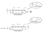
- a graded profile 905 which maps grating height as a function of distance D may be applied to a trailing edge of a DOE (e.g., DOE 1 ).
- the trailing edge is at the end of the DOE at which propagating light exits the grating and is indicated by reference numeral 910 .
- the edge 910 may typically encompass some portion of the DOE that is adjacent to the interface between the DOEs as shown in FIG. 9 .
- the grating height h is decreased from a full height so that the grating becomes increasingly shallow (i.e., grating height is reduced) as distance to the trailing edge decreases.
- FIG. 10 A representative portion of the DOE to which the graded profile 905 is applied is shown in FIG. 10 . While slanted gratings are shown in FIG. 10 , it is emphasized that the illustrated concepts are equally applicable to straight gratings. As shown, the height of respective grating bars in the DOE is reduced to become more shallow in the direction of propagation so that the m th grating bar 1010 has a greater height than that of the n th grating bar 1015 . In some implementations, the height is reduced to zero or near zero at or near the point of interface with the next DOE (e.g., DOE 2 ). That is, the gratings may become so small that they transition into a smooth surface.
- DOE e.g., DOE 2
- non-zero values at or near such interface may also be utilized in some implementations. While “near” is a relative term, it will be appreciated that various values for the smallest grating height and its location relative to the trailing edge may be utilized for a given implementation while still achieving a target optical resolution and increased tolerance for height mismatch in manufacturing. In addition, given that the heights discussed herein are in the submicron range, terms such as “near zero” are used in recognition, as discussed above, that characterization of very small grating heights is not generally possible using tools available in a manufacturing environment.
- the illustrative graded profile 905 applies an approximately linear curve to a portion of a DOE at its trailing edge in which grating bars are smoothly reduced in height in order to avoid any abrupt or sudden transition to the downstream DOE.
- non-linear curves may also be used for the graded profile 905 in some implementations.
- the graded profile may be stepped so that groups of grating bars share the same height, and a downstream group of grating bars have decreased height relative to an upstream group.
- the particular upstream point of transition 912 in the DOE from full height gratings to the decreasing height gratings can vary by implementation and may depend on target optical characteristics and the configuration of the DOE including size and shape, and grating attributes such as height, refractive index, fill ratio, and configuration (i.e., whether straight or slanted grating bars), for example.
- a graded profile 915 may be applied to a leading edge of a DOE (e.g., DOE 2 ) as indicated by reference numeral 920 .
- the leading edge is located at the end of the DOE at which propagating light enters the grating.
- the grating height h is increased from shallow height to full height so that the grating becomes increasingly deep as the distance away from the leading edge increases.
- the graded profile 915 may be approximately linear in typical implementations, but non-linear profiles may also by utilized in other implementations.
- the particular downstream point of transition 922 in the DOE from shallow to full height grating bars (and accordingly the slope of the graded curve) can vary by implementation.
- FIG. 11 A representative portion of the DOE to which the graded profile 915 applied is shown in FIG. 11 . While straight gratings are shown in FIG. 11 , it is emphasized that the illustrated concepts are equally applicable to slanted gratings. As shown, the height of respective gratings in the DOE is increased in the direction of propagation so that the n th grating bar 1115 has a greater height than that of the m th grating bar 1110 . Typically, the height is increased from zero or near zero at or near the point of interface with the upstream DOE (e.g., DOE 1 ). However, non-zero starting values for grating height at or near such interface may also be utilized in some implementations. For example, the leading edge may include a smooth surface adjacent to the interface between the DOEs that transitions to full height gratings, while in other implementations, the leading edge can start with shallow gratings.
- the leading edge may include a smooth surface adjacent to the interface between the DOEs that transitions to full height grat
- the graded profiles for respective leading and trailing edges of the DOEs may be applied to both the transition between DOE 1 and DOE 2 (i.e., the in-coupling grating and the intermediate grating that expands the exit pupil in the first direction) as well as the transition between DOE 2 and DOE 3 (in which DOE 3 expands the exit pupil in the second direction).
- DOE 3 is configured as an apodized grating (i.e., a grating in which the grating's modulation index gradually increases and then decreases along the length of the grating)
- portions or all of the grating may already be sufficiently shallow to ensure a smooth transition from DOE 2 without application of the graded profile.
- FIG. 12 shows an illustrative arrangement for DOE fabrication using a mask 1205 that moves relative to a photosensitive grating substrate 1210 within an enclosure 1215 .
- a reactive ion etching plasma 1220 is used to adjust the thickness of the etching on the grating substrate at various positions by moving the substrate relative to mask using, for example, a computer-controller stepper functionality or other suitable control system.
- the etching may be performed using a reactive ion beam etching (RIBE).
- RIBE reactive ion beam etching
- ion beam etching may be utilized in various implementations including, for example, such as magnetron reactive ion etching (MRIE), high density plasma etching (HDP), transformer coupled plasma etching (TCP), inductively coupled plasma etching (ICP), and electron resonance plasma etching (ECR).
- MEM magnetron reactive ion etching
- HDP high density plasma etching
- TCP transformer coupled plasma etching
- ICP inductively coupled plasma etching
- ECR electron resonance plasma etching
- grating depth can be varied as a function of position over the extent of the substrate to thereby enable the above-described graded profiles to be incorporated on the substrate.
- the resulting microstructure on the substrate may be replicated for mass production in a lightweight polymer material using one of cast-and-cure, embossing, compression molding, or compression injection molding, for example.
- FIG. 13 is a flowchart 13 of an illustrative method 1300 .
- the methods or steps shown in the flowchart and described in the accompanying text are not constrained to a particular order or sequence.
- some of the methods or steps thereof can occur or be performed concurrently and not all the methods or steps have to be performed in a given implementation depending on the requirements of such implementation and some methods or steps may be optionally utilized.
- step 1305 light is received at an in-coupling DOE.
- the in-coupling grating is disposed in an EPE and is configured with a graded trailing edge, as described above, on which full height gratings smoothly transition to a smooth surface near the interface with the downstream intermediate DOE that is disposed in the EPE.
- step 1310 the exit pupil of the received light is expanded along a first coordinate axis in the intermediate DOE.
- the intermediate DOE is configured with a graded leading edge on which a smooth surface near the interface smoothly transitions to full height gratings.
- the exit pupil is expanded in an out-coupling DOE which outputs light with an expanded exit pupil relative to the received light at the in-coupling DOE along the first and second coordinate axes in step 1320 .
- the intermediate DOE is configured with a graded trailing edge on which full height gratings smoothly transition to a smooth surface near the interface with the downstream out-coupling DOE.
- the out-coupling DOE may also be configured with a graded leading edge that receives light coupled from the intermediate DOE.
- the out-coupling may be apodized and have sufficiently shallow gratings that application of a graded profile to its leading edge may be unnecessary.
- DOEs with graded edges may be incorporated into a display system that is utilized in a virtual or mixed reality display device.
- a virtual or mixed reality display device may take any suitable form, including but not limited to near-eye devices such as an HMD device.
- a see-through display may be used in some implementations while an opaque (i.e., non-see-through) display using a camera-based pass-through or outward facing sensor, for example, may be used in other implementations.
- FIG. 14 shows one particular illustrative example of a see-through, mixed reality or virtual reality display system 1400
- FIG. 15 shows a functional block diagram of the system 1400 .
- Display system 1400 comprises one or more lenses 1402 that form a part of a see-through display subsystem 1404 , such that images may be displayed using lenses 1402 (e.g. using projection onto lenses 1402 , one or more waveguide systems incorporated into the lenses 1402 , and/or in any other suitable manner).
- Display system 1400 further comprises one or more outward-facing image sensors 1406 configured to acquire images of a background scene and/or physical environment being viewed by a user, and may include one or more microphones 1408 configured to detect sounds, such as voice commands from a user.
- Outward-facing image sensors 1406 may include one or more depth sensors and/or one or more two-dimensional image sensors.
- a mixed reality or virtual reality display system instead of incorporating a see-through display subsystem, may display mixed reality or virtual reality images through a viewfinder mode for an outward-facing image sensor.
- the display system 1400 may further include a gaze detection subsystem 1410 configured for detecting a direction of gaze of each eye of a user or a direction or location of focus, as described above. Gaze detection subsystem 1410 may be configured to determine gaze directions of each of a user's eyes in any suitable manner.
- a gaze detection subsystem 1410 includes one or more glint sources 1412 , such as infrared light sources, that are configured to cause a glint of light to reflect from each eyeball of a user, and one or more image sensors 1414 , such as inward-facing sensors, that are configured to capture an image of each eyeball of the user. Changes in the glints from the user's eyeballs and/or a location of a user's pupil, as determined from image data gathered using the image sensor(s) 1414 , may be used to determine a direction of gaze.
- glint sources 1412 such as infrared light sources
- image sensors 1414 such as inward-facing sensors
- Gaze detection subsystem 1410 may have any suitable number and arrangement of light sources and image sensors. In some implementations, the gaze detection subsystem 1410 may be omitted.
- the display system 1400 may also include additional sensors.
- display system 1400 may comprise a global positioning system (GPS) subsystem 1416 to allow a location of the display system 1400 to be determined. This may help to identify real world objects, such as buildings, etc. that may be located in the user's adjoining physical environment.
- GPS global positioning system
- the display system 1400 may further include one or more motion sensors 1418 (e.g., inertial, multi-axis gyroscopic, or acceleration sensors) to detect movement and position/orientation/pose of a user's head when the user is wearing the system as part of a mixed reality or virtual reality HMD device.
- Motion data may be used, potentially along with eye-tracking glint data and outward-facing image data, for gaze detection, as well as for image stabilization to help correct for blur in images from the outward-facing image sensor(s) 1406 .
- the use of motion data may allow changes in gaze location to be tracked even if image data from outward-facing image sensor(s) 1406 cannot be resolved.
- motion sensors 1418 as well as microphone(s) 1408 and gaze detection subsystem 1410 , also may be employed as user input devices, such that a user may interact with the display system 1400 via gestures of the eye, neck and/or head, as well as via verbal commands in some cases. It may be understood that sensors illustrated in FIGS. 14 and 15 and described in the accompanying text are included for the purpose of example and are not intended to be limiting in any manner, as any other suitable sensors and/or combination of sensors may be utilized to meet the needs of a particular implementation.
- biometric sensors e.g., for detecting heart and respiration rates, blood pressure, brain activity, body temperature, etc.
- environmental sensors e.g., for detecting temperature, humidity, elevation, UV (ultraviolet) light levels, etc.
- biometric sensors e.g., for detecting heart and respiration rates, blood pressure, brain activity, body temperature, etc.
- environmental sensors e.g., for detecting temperature, humidity, elevation, UV (ultraviolet) light levels, etc.
- the display system 1400 can further include a controller 1420 having a logic subsystem 1422 and a data storage subsystem 1424 in communication with the sensors, gaze detection subsystem 1410 , display subsystem 1404 , and/or other components through a communications subsystem 1426 .
- the communications subsystem 1426 can also facilitate the display system being operated in conjunction with remotely located resources, such as processing, storage, power, data, and services. That is, in some implementations, an HMD device can be operated as part of a system that can distribute resources and capabilities among different components and subsystems.
- the storage subsystem 1424 may include instructions stored thereon that are executable by logic subsystem 1422 , for example, to receive and interpret inputs from the sensors, to identify location and movements of a user, to identify real objects using surface reconstruction and other techniques, and dim/fade the display based on distance to objects so as to enable the objects to be seen by the user, among other tasks.
- the display system 1400 is configured with one or more audio transducers 1428 (e.g., speakers, earphones, etc.) so that audio can be utilized as part of a mixed reality or virtual reality experience.
- a power management subsystem 1430 may include one or more batteries 1432 and/or protection circuit modules (PCMs) and an associated charger interface 1434 and/or remote power interface for supplying power to components in the display system 1400 .
- PCMs protection circuit modules
- the display system 1400 is described for the purpose of example, and thus is not meant to be limiting. It is to be further understood that the display device may include additional and/or alternative sensors, cameras, microphones, input devices, output devices, etc. than those shown without departing from the scope of the present arrangement. Additionally, the physical configuration of a display device and its various sensors and subcomponents may take a variety of different forms without departing from the scope of the present arrangement.
- an EPE incorporating the present DOEs with graded edges can be used in a mobile or portable electronic device 1600 , such as a mobile phone, smartphone, personal digital assistant (PDA), communicator, portable Internet appliance, hand-held computer, digital video or still camera, wearable computer, computer game device, specialized bring-to-the-eye product for viewing, or other portable electronic device.
- the portable device 1600 includes a housing 1605 to house a communication module 1610 for receiving and transmitting information from and to an external device, or a remote system or service (not shown).
- the portable device 1600 may also include an image processing module 1615 for handling the received and transmitted information, and a virtual display system 1620 to support viewing of images.
- the virtual display system 1620 can include a micro-display or an imager 1625 and an optical engine 1630 .
- the image processing module 1615 may be operatively connected to the optical engine 1630 to provide image data, such as video data, to the imager 1625 to display an image thereon.
- An EPE 1635 using one or more DOEs with graded edges can be optically linked to an optical engine 1630 .
- An EPE using one or more DOEs with graded edges may also be utilized in non-portable devices, such as a gaming devices, multimedia consoles, personal computers, vending machines, smart appliances, Internet-connected devices, and home appliances, such as an oven, microwave oven and other appliances, and other non-portable devices.
- non-portable devices such as a gaming devices, multimedia consoles, personal computers, vending machines, smart appliances, Internet-connected devices, and home appliances, such as an oven, microwave oven and other appliances, and other non-portable devices.
- An example includes an optical system, comprising: a substrate of optical material; a first diffractive optical element (DOE) disposed on the substrate and configured as an in-coupling grating to receive, as an input, one or more optical beams that propagate in the first DOE and exit at a trailing edge of the first DOE; and a second DOE disposed on the substrate and configured for pupil expansion of the one or more optical beams along a first direction, in which the trailing edge of the first DOE is located on the substrate at an interface with the second DOE, wherein the one or more optical beams exiting at the trailing edge, enter a leading edge of the second DOE, and wherein the trailing edge and leading edge are graded so that a grating height of each of the first DOE and the second DOE increases as a function of distance from the interface.
- DOE diffractive optical element
- the optical system further includes a third DOE disposed on the substrate and configured for pupil expansion of the optical beams along a second direction, and further configured as an out-coupling grating to couple, as an output from the substrate, one or more optical beams with expanded pupil relative to the input.
- the grating height in the first DOE decreases approximately linearly from a full height upstream from the trailing edge to a shallow height at the trailing edge of the first DOE.
- the grating height in the first DOE decreases approximately linearly from a full height upstream from the trailing edge to zero height at the trailing edge of the first DOE.
- the grating height in the second DOE increases approximately linearly from a shallow height at the leading edge to a full height downstream from the leading edge.
- either the first DOE or second DOE is a straight diffraction grating or a slanted diffraction grating.
- the one or more optical beams received as the input emanate as a virtual image produced by a micro-display or imager.
- a further example includes an electronic device, comprising: a data processing unit; an optical engine operatively connected to the data processing unit for receiving image data from the data processing unit; an imager operatively connected to the optical engine to form images based on the image data and to generate one or more input optical beams incorporating the images; and an exit pupil expander, responsive to the one or more input optical beams, comprising a structure on which multiple diffractive optical elements (DOEs) are disposed, in which the exit pupil expander is configured to provide one or more output optical beams, using one or more of the DOEs, as one or more near eye virtual displays with an expanded exit pupil, and in which light enters at a leading edge of a DOE and exits at a trailing edge of a DOE and at least one of the DOEs has a portion with a graded profile so that grating height linearly increases as a function of distance from the leading edge or the trailing edge over the portion.
- DOEs diffractive optical elements
- the exit pupil expander provides pupil expansion in two directions.
- the structure comprises a waveguide.
- the imager includes one of light emitting diode, liquid crystal on silicon device, organic light emitting diode array, or micro-electro mechanical system device.
- the imager comprises a micro-display operating in one of transmission, reflection, or emission.
- the electronic device is implemented in a head mounted display device or portable electronic device.
- each of the one or more input optical beams is produced by a corresponding one or more sources.
- a further example includes a method, comprising: receiving light at an input-coupling diffractive optical element (DOE) disposed in an exit pupil expander; expanding an exit pupil of the received light along a first coordinate axis in an intermediate DOE disposed in the exit pupil expander; expanding the exit pupil along a second coordinate axis in an output-coupling DOE disposed in the exit pupil expander; and outputting light with an expanded exit pupil relative to the received light at the input-coupling DOE along the first and second coordinate axes using the output-coupling DOE, in which light exits the input-coupling DOE at a first graded trailing edge on which full height gratings transition to a smooth surface on the input-coupling DOE adjacent to a first interface between the in-coupling DOE and the intermediate DOE, and in which light exiting the input-coupling DOE enters the intermediate DOE at a graded leading edge on which a smooth surface on the intermediate DOE adjacent to the first interface transitions to full height gratings, and in which light exits the intermediate DOE at a second grade
- the transitions are gradual to minimize discontinuity at the interface so as to reduce impairment of optical resolution or reduce phase change in light coupled between the in-coupling DOE and intermediate DOE or between the intermediate DOE and the out-coupling DOE.
- the input-coupling DOE, the intermediate DOE, or the output-coupling DOE is formed with a polymer that is molded from a substrate that is etched using ion beam etching with a moving mask.
- at least a portion of the out-coupling DOE is an apodized diffraction grating having shallow grooves relative to the input-coupling DOE or the intermediate DOE.
- the method is performed in a near eye optical system.
- the output light provides a virtual display to a user of the near eye optical system.
Abstract
In an optical system that includes a waveguide with multiple diffractive optical elements (DOEs) incorporating diffraction gratings, light exiting a trailing edge of an upstream DOE enters a leading edge of a downstream DOE. One or more of the DOEs may include a leading and/or a trailing edge that have a graded profile. At a graded trailing edge of an upstream DOE, grating height smoothly decreases from full height to shallow height as a function of the proximity to the trailing edge. At a graded leading edge of the downstream DOE grating height smoothly increases from shallow height to full height as a function of distance away from the leading edge. By reducing a sharp boundary at the interface between the upstream and downstream DOEs, the graded profiles of the DOE edges enable optical resolution to be maintained decreasing sensitivity to misalignment between the DOEs that may occur during manufacturing.
Description
Diffractive optical elements (DOEs) are optical elements with a periodic structure which are commonly utilized in applications ranging from bio-technology, material processing, sensing, and testing to technical optics and optical metrology. By incorporating DOEs in an optical field of a laser or emissive display, for example, the light's “shape” can be controlled and changed flexibly according to application needs.
In an optical system that includes a waveguide with multiple diffractive optical elements (DOEs) incorporating diffraction gratings, light exiting a trailing edge of an upstream DOE enters a leading edge of a downstream DOE in the waveguide. One or more of the DOEs may include a leading and/or a trailing edge that have a graded profile. At a graded trailing edge of an upstream DOE, grating height smoothly decreases from full height to shallow height as a function of the proximity to the trailing edge. At a graded leading edge of the downstream DOE, grating height smoothly increases from shallow height to full height as a function of distance away from the leading edge. By reducing a sharp boundary at the interface between the upstream and downstream DOEs, the graded profiles applied to the DOE edges enable optical resolution to be maintained in the waveguide while decreasing sensitivity to misalignment between the DOEs that may occur during manufacturing.
This Summary is provided to introduce a selection of concepts in a simplified form that are further described below in the Detailed Description. This Summary is not intended to identify key features or essential features of the claimed subject matter, nor is it intended to be used as an aid in determining the scope of the claimed subject matter. Furthermore, the claimed subject matter is not limited to implementations that solve any or all disadvantages noted in any part of this disclosure.
Like reference numerals indicate like elements in the drawings. Elements are not drawn to scale unless otherwise indicated.
In a near eye display system the imager does not actually shine the images on a surface such as glass lenses to create the visual display for the user. This is not feasible because the human eye cannot focus on something that is that close. Indeed, rather than create a visible image on a surface, the near eye display system 100 uses the pupil forming optics 125 to form a pupil and the eye 115 acts as the last element in the optical chain and converts the light from the pupil into an image on the eye's retina as a virtual display.
The waveguide 130 facilitates light transmission between the imager and the eye. One or more waveguides can be utilized in the near eye display system because they are transparent and because they are generally small and lightweight (which is desirable in applications such as HMD devices where size and weight is generally sought to be minimized for reasons of performance and user comfort). For example, the waveguide 130 can enable the imager 105 to be located out the way, for example, on the side of the head, leaving only a relatively small, light, and transparent waveguide optical element in front of the eyes. In one implementation, the waveguide 130 operates using a principle of total internal reflection, as shown in FIG. 2 , so that light can be coupled among the various optical elements in the system 100.
The EPE 305 is configured, in this illustrative example, to support binocular operation for both the left and right eyes (components which may be utilized for stereoscopic operation such as scanning mirrors, lenses, filters, beam splitters, MEMS devices, or the like are not shown in FIG. 3 for sake of clarity in exposition). Accordingly, the EPE 305 utilizes two out-coupling gratings, 310 L and 310 R that are supported on a waveguide 330 and a central in-coupling grating 340. The in-coupling and out-coupling gratings may be configured using multiple DOEs, as described in the illustrative example below.
As shown in FIG. 4 , the EPE 305 may be configured to provide an expanded exit pupil in two directions (i.e., along each of a first and second coordinate axis). As shown, the exit pupil is expanded in both the vertical and horizontal directions. It may be understood that the terms “direction,” “horizontal,” and “vertical” are used primarily to establish relative orientations in the illustrative examples shown and described herein for ease of description. These terms may be intuitive for a usage scenario in which the user of the near eye display device is upright and forward facing, but less intuitive for other usage scenarios. Accordingly, the listed terms are not to be construed to limit the scope of the configurations (and usage scenarios therein) of the present DOEs with graded edges.
As shown in FIGS. 6 and 7 , respectively, the DOEs 505, 510, and 515 can be configured using straight (i.e., non-slanted) grating features 600 (typically referred to as grating bars or simply “gratings”), that are formed in a substrate 605, or using slanted grating features 700 formed in a substrate 705. The grating period is represented by d, the grating height by h, bar width by c, and the filling factor by f. The slanted grating features may be described by slant angles α1 and α2. In one exemplary embodiment, for the non-graded portions of DOE 1, d=390 nm, c=d/2, h=300 nm, α1=α2=250 degrees, f=0.5 c, and the refractive index of the substrate material is approximately 1.71. In other implementations, ranges of suitable values may include d=250 nm-450 nm, h=200 nm-400 nm, f=0.3-0, and α1=30-50 degrees, with refractive indices of 1.7 to 1.9.
As discussed above, the DOE structures contain submicron features and the optical wavelength in the waveguide is relatively small, for example, on the order of 250-400 nm. As a result, discontinuities between the surfaces of the DOEs can have a large impact on optical resolution, for example, as measured by MTF (modulation transfer function). As shown in FIG. 8 , a small gap height 805 at the interface between the DOEs (as indicated by reference numeral 810) relative to the grating height can negatively impair optical resolution. Such impairment may reduce the functionality of a near eye display system in which the DOEs are used and/or result in vestibular discomfort for a near eye system user in some cases. For example, a gap height of 5 nm can decrease optical resolution by as much 50% in some cases. The grating features in a DOE can also behave as aperture features which may introduce undesirable phase changes in the light as it propagates between DOEs.
Accordingly, the manufacturing processes used for conventional DOEs typically needs to be highly accurate so that nanometer level variations in grating height do not occur. Such level of accuracy may imply that the measurement accuracy used for characterization and quality control, for example, may need to be on the order of 0.5 nm. Tools having such accuracy are generally unavailable in manufacturing environments, particularly for volume production.
The DOEs 505, 510, and 515 with graded edges facilitate increased tolerance for gap height mismatch in manufacturing while still maintaining a desired optical resolution. For example, as shown in FIG. 9 , a graded profile 905 which maps grating height as a function of distance D may be applied to a trailing edge of a DOE (e.g., DOE 1). The trailing edge is at the end of the DOE at which propagating light exits the grating and is indicated by reference numeral 910. The edge 910 may typically encompass some portion of the DOE that is adjacent to the interface between the DOEs as shown in FIG. 9 . At some transition point 912 upstream from the trailing edge, the grating height h is decreased from a full height so that the grating becomes increasingly shallow (i.e., grating height is reduced) as distance to the trailing edge decreases.
A representative portion of the DOE to which the graded profile 905 is applied is shown in FIG. 10 . While slanted gratings are shown in FIG. 10 , it is emphasized that the illustrated concepts are equally applicable to straight gratings. As shown, the height of respective grating bars in the DOE is reduced to become more shallow in the direction of propagation so that the mth grating bar 1010 has a greater height than that of the nth grating bar 1015. In some implementations, the height is reduced to zero or near zero at or near the point of interface with the next DOE (e.g., DOE 2). That is, the gratings may become so small that they transition into a smooth surface. However, non-zero values at or near such interface may also be utilized in some implementations. While “near” is a relative term, it will be appreciated that various values for the smallest grating height and its location relative to the trailing edge may be utilized for a given implementation while still achieving a target optical resolution and increased tolerance for height mismatch in manufacturing. In addition, given that the heights discussed herein are in the submicron range, terms such as “near zero” are used in recognition, as discussed above, that characterization of very small grating heights is not generally possible using tools available in a manufacturing environment.
The illustrative graded profile 905 applies an approximately linear curve to a portion of a DOE at its trailing edge in which grating bars are smoothly reduced in height in order to avoid any abrupt or sudden transition to the downstream DOE. However, non-linear curves may also be used for the graded profile 905 in some implementations. For example, the graded profile may be stepped so that groups of grating bars share the same height, and a downstream group of grating bars have decreased height relative to an upstream group. The particular upstream point of transition 912 in the DOE from full height gratings to the decreasing height gratings (and accordingly, the slope of the graded curve) can vary by implementation and may depend on target optical characteristics and the configuration of the DOE including size and shape, and grating attributes such as height, refractive index, fill ratio, and configuration (i.e., whether straight or slanted grating bars), for example.
Returning to FIG. 9 , a graded profile 915 may be applied to a leading edge of a DOE (e.g., DOE 2) as indicated by reference numeral 920. The leading edge is located at the end of the DOE at which propagating light enters the grating. At or near the leading edge, or at some point upstream from the leading edge, the grating height h is increased from shallow height to full height so that the grating becomes increasingly deep as the distance away from the leading edge increases.
As with the graded profile 905, the graded profile 915 may be approximately linear in typical implementations, but non-linear profiles may also by utilized in other implementations. The particular downstream point of transition 922 in the DOE from shallow to full height grating bars (and accordingly the slope of the graded curve) can vary by implementation.
A representative portion of the DOE to which the graded profile 915 applied is shown in FIG. 11 . While straight gratings are shown in FIG. 11 , it is emphasized that the illustrated concepts are equally applicable to slanted gratings. As shown, the height of respective gratings in the DOE is increased in the direction of propagation so that the nth grating bar 1115 has a greater height than that of the mth grating bar 1110. Typically, the height is increased from zero or near zero at or near the point of interface with the upstream DOE (e.g., DOE 1). However, non-zero starting values for grating height at or near such interface may also be utilized in some implementations. For example, the leading edge may include a smooth surface adjacent to the interface between the DOEs that transitions to full height gratings, while in other implementations, the leading edge can start with shallow gratings.
The graded profiles for respective leading and trailing edges of the DOEs may be applied to both the transition between DOE 1 and DOE 2 (i.e., the in-coupling grating and the intermediate grating that expands the exit pupil in the first direction) as well as the transition between DOE 2 and DOE 3 (in which DOE 3 expands the exit pupil in the second direction). However, in some implementations in which DOE 3 is configured as an apodized grating (i.e., a grating in which the grating's modulation index gradually increases and then decreases along the length of the grating), portions or all of the grating may already be sufficiently shallow to ensure a smooth transition from DOE 2 without application of the graded profile.
By controlling the exposure of the substrate to the plasma through the mask aperture, grating depth can be varied as a function of position over the extent of the substrate to thereby enable the above-described graded profiles to be incorporated on the substrate. The resulting microstructure on the substrate may be replicated for mass production in a lightweight polymer material using one of cast-and-cure, embossing, compression molding, or compression injection molding, for example.
In step 1305, light is received at an in-coupling DOE. The in-coupling grating is disposed in an EPE and is configured with a graded trailing edge, as described above, on which full height gratings smoothly transition to a smooth surface near the interface with the downstream intermediate DOE that is disposed in the EPE. In step 1310, the exit pupil of the received light is expanded along a first coordinate axis in the intermediate DOE. The intermediate DOE is configured with a graded leading edge on which a smooth surface near the interface smoothly transitions to full height gratings.
In step 1315, the exit pupil is expanded in an out-coupling DOE which outputs light with an expanded exit pupil relative to the received light at the in-coupling DOE along the first and second coordinate axes in step 1320. The intermediate DOE is configured with a graded trailing edge on which full height gratings smoothly transition to a smooth surface near the interface with the downstream out-coupling DOE. In some implementations, the out-coupling DOE may also be configured with a graded leading edge that receives light coupled from the intermediate DOE. In other implementations, the out-coupling may be apodized and have sufficiently shallow gratings that application of a graded profile to its leading edge may be unnecessary.
DOEs with graded edges may be incorporated into a display system that is utilized in a virtual or mixed reality display device. Such device may take any suitable form, including but not limited to near-eye devices such as an HMD device. A see-through display may be used in some implementations while an opaque (i.e., non-see-through) display using a camera-based pass-through or outward facing sensor, for example, may be used in other implementations. FIG. 14 shows one particular illustrative example of a see-through, mixed reality or virtual reality display system 1400, and FIG. 15 shows a functional block diagram of the system 1400. Display system 1400 comprises one or more lenses 1402 that form a part of a see-through display subsystem 1404, such that images may be displayed using lenses 1402 (e.g. using projection onto lenses 1402, one or more waveguide systems incorporated into the lenses 1402, and/or in any other suitable manner). Display system 1400 further comprises one or more outward-facing image sensors 1406 configured to acquire images of a background scene and/or physical environment being viewed by a user, and may include one or more microphones 1408 configured to detect sounds, such as voice commands from a user. Outward-facing image sensors 1406 may include one or more depth sensors and/or one or more two-dimensional image sensors. In alternative arrangements, as noted above, a mixed reality or virtual reality display system, instead of incorporating a see-through display subsystem, may display mixed reality or virtual reality images through a viewfinder mode for an outward-facing image sensor.
The display system 1400 may further include a gaze detection subsystem 1410 configured for detecting a direction of gaze of each eye of a user or a direction or location of focus, as described above. Gaze detection subsystem 1410 may be configured to determine gaze directions of each of a user's eyes in any suitable manner. For example, in the illustrative example shown, a gaze detection subsystem 1410 includes one or more glint sources 1412, such as infrared light sources, that are configured to cause a glint of light to reflect from each eyeball of a user, and one or more image sensors 1414, such as inward-facing sensors, that are configured to capture an image of each eyeball of the user. Changes in the glints from the user's eyeballs and/or a location of a user's pupil, as determined from image data gathered using the image sensor(s) 1414, may be used to determine a direction of gaze.
In addition, a location at which gaze lines projected from the user's eyes intersect the external display may be used to determine an object at which the user is gazing (e.g. a displayed virtual object and/or real background object). Gaze detection subsystem 1410 may have any suitable number and arrangement of light sources and image sensors. In some implementations, the gaze detection subsystem 1410 may be omitted.
The display system 1400 may also include additional sensors. For example, display system 1400 may comprise a global positioning system (GPS) subsystem 1416 to allow a location of the display system 1400 to be determined. This may help to identify real world objects, such as buildings, etc. that may be located in the user's adjoining physical environment.
The display system 1400 may further include one or more motion sensors 1418 (e.g., inertial, multi-axis gyroscopic, or acceleration sensors) to detect movement and position/orientation/pose of a user's head when the user is wearing the system as part of a mixed reality or virtual reality HMD device. Motion data may be used, potentially along with eye-tracking glint data and outward-facing image data, for gaze detection, as well as for image stabilization to help correct for blur in images from the outward-facing image sensor(s) 1406. The use of motion data may allow changes in gaze location to be tracked even if image data from outward-facing image sensor(s) 1406 cannot be resolved.
In addition, motion sensors 1418, as well as microphone(s) 1408 and gaze detection subsystem 1410, also may be employed as user input devices, such that a user may interact with the display system 1400 via gestures of the eye, neck and/or head, as well as via verbal commands in some cases. It may be understood that sensors illustrated in FIGS. 14 and 15 and described in the accompanying text are included for the purpose of example and are not intended to be limiting in any manner, as any other suitable sensors and/or combination of sensors may be utilized to meet the needs of a particular implementation. For example, biometric sensors (e.g., for detecting heart and respiration rates, blood pressure, brain activity, body temperature, etc.) or environmental sensors (e.g., for detecting temperature, humidity, elevation, UV (ultraviolet) light levels, etc.) may be utilized in some implementations.
The display system 1400 can further include a controller 1420 having a logic subsystem 1422 and a data storage subsystem 1424 in communication with the sensors, gaze detection subsystem 1410, display subsystem 1404, and/or other components through a communications subsystem 1426. The communications subsystem 1426 can also facilitate the display system being operated in conjunction with remotely located resources, such as processing, storage, power, data, and services. That is, in some implementations, an HMD device can be operated as part of a system that can distribute resources and capabilities among different components and subsystems.
The storage subsystem 1424 may include instructions stored thereon that are executable by logic subsystem 1422, for example, to receive and interpret inputs from the sensors, to identify location and movements of a user, to identify real objects using surface reconstruction and other techniques, and dim/fade the display based on distance to objects so as to enable the objects to be seen by the user, among other tasks.
The display system 1400 is configured with one or more audio transducers 1428 (e.g., speakers, earphones, etc.) so that audio can be utilized as part of a mixed reality or virtual reality experience. A power management subsystem 1430 may include one or more batteries 1432 and/or protection circuit modules (PCMs) and an associated charger interface 1434 and/or remote power interface for supplying power to components in the display system 1400.
It may be appreciated that the display system 1400 is described for the purpose of example, and thus is not meant to be limiting. It is to be further understood that the display device may include additional and/or alternative sensors, cameras, microphones, input devices, output devices, etc. than those shown without departing from the scope of the present arrangement. Additionally, the physical configuration of a display device and its various sensors and subcomponents may take a variety of different forms without departing from the scope of the present arrangement.
As shown in FIG. 16 , an EPE incorporating the present DOEs with graded edges can be used in a mobile or portable electronic device 1600, such as a mobile phone, smartphone, personal digital assistant (PDA), communicator, portable Internet appliance, hand-held computer, digital video or still camera, wearable computer, computer game device, specialized bring-to-the-eye product for viewing, or other portable electronic device. As shown, the portable device 1600 includes a housing 1605 to house a communication module 1610 for receiving and transmitting information from and to an external device, or a remote system or service (not shown).
The portable device 1600 may also include an image processing module 1615 for handling the received and transmitted information, and a virtual display system 1620 to support viewing of images. The virtual display system 1620 can include a micro-display or an imager 1625 and an optical engine 1630. The image processing module 1615 may be operatively connected to the optical engine 1630 to provide image data, such as video data, to the imager 1625 to display an image thereon. An EPE 1635 using one or more DOEs with graded edges can be optically linked to an optical engine 1630.
An EPE using one or more DOEs with graded edges may also be utilized in non-portable devices, such as a gaming devices, multimedia consoles, personal computers, vending machines, smart appliances, Internet-connected devices, and home appliances, such as an oven, microwave oven and other appliances, and other non-portable devices.
Various exemplary embodiments of the present diffractive optical elements with graded edges are now presented by way of illustration and not as an exhaustive list of all embodiments. An example includes an optical system, comprising: a substrate of optical material; a first diffractive optical element (DOE) disposed on the substrate and configured as an in-coupling grating to receive, as an input, one or more optical beams that propagate in the first DOE and exit at a trailing edge of the first DOE; and a second DOE disposed on the substrate and configured for pupil expansion of the one or more optical beams along a first direction, in which the trailing edge of the first DOE is located on the substrate at an interface with the second DOE, wherein the one or more optical beams exiting at the trailing edge, enter a leading edge of the second DOE, and wherein the trailing edge and leading edge are graded so that a grating height of each of the first DOE and the second DOE increases as a function of distance from the interface.
In another example, the optical system further includes a third DOE disposed on the substrate and configured for pupil expansion of the optical beams along a second direction, and further configured as an out-coupling grating to couple, as an output from the substrate, one or more optical beams with expanded pupil relative to the input. In another example, the grating height in the first DOE decreases approximately linearly from a full height upstream from the trailing edge to a shallow height at the trailing edge of the first DOE. In another example, the grating height in the first DOE decreases approximately linearly from a full height upstream from the trailing edge to zero height at the trailing edge of the first DOE. In another example, the grating height in the second DOE increases approximately linearly from a shallow height at the leading edge to a full height downstream from the leading edge. In another example, either the first DOE or second DOE is a straight diffraction grating or a slanted diffraction grating. In another example, the one or more optical beams received as the input emanate as a virtual image produced by a micro-display or imager.
A further example includes an electronic device, comprising: a data processing unit; an optical engine operatively connected to the data processing unit for receiving image data from the data processing unit; an imager operatively connected to the optical engine to form images based on the image data and to generate one or more input optical beams incorporating the images; and an exit pupil expander, responsive to the one or more input optical beams, comprising a structure on which multiple diffractive optical elements (DOEs) are disposed, in which the exit pupil expander is configured to provide one or more output optical beams, using one or more of the DOEs, as one or more near eye virtual displays with an expanded exit pupil, and in which light enters at a leading edge of a DOE and exits at a trailing edge of a DOE and at least one of the DOEs has a portion with a graded profile so that grating height linearly increases as a function of distance from the leading edge or the trailing edge over the portion.
In another example, the exit pupil expander provides pupil expansion in two directions. In another example, the structure comprises a waveguide. In another example, the imager includes one of light emitting diode, liquid crystal on silicon device, organic light emitting diode array, or micro-electro mechanical system device. In another example, the imager comprises a micro-display operating in one of transmission, reflection, or emission. In another example, the electronic device is implemented in a head mounted display device or portable electronic device. In another example, each of the one or more input optical beams is produced by a corresponding one or more sources.
A further example includes a method, comprising: receiving light at an input-coupling diffractive optical element (DOE) disposed in an exit pupil expander; expanding an exit pupil of the received light along a first coordinate axis in an intermediate DOE disposed in the exit pupil expander; expanding the exit pupil along a second coordinate axis in an output-coupling DOE disposed in the exit pupil expander; and outputting light with an expanded exit pupil relative to the received light at the input-coupling DOE along the first and second coordinate axes using the output-coupling DOE, in which light exits the input-coupling DOE at a first graded trailing edge on which full height gratings transition to a smooth surface on the input-coupling DOE adjacent to a first interface between the in-coupling DOE and the intermediate DOE, and in which light exiting the input-coupling DOE enters the intermediate DOE at a graded leading edge on which a smooth surface on the intermediate DOE adjacent to the first interface transitions to full height gratings, and in which light exits the intermediate DOE at a second graded trailing edge on which full height gratings transition to a smooth surface on the intermediate DOE adjacent to a second interface between the intermediate DOE and the out-coupling DOE.
In another example, the transitions are gradual to minimize discontinuity at the interface so as to reduce impairment of optical resolution or reduce phase change in light coupled between the in-coupling DOE and intermediate DOE or between the intermediate DOE and the out-coupling DOE. In another example, the input-coupling DOE, the intermediate DOE, or the output-coupling DOE is formed with a polymer that is molded from a substrate that is etched using ion beam etching with a moving mask. In another example, at least a portion of the out-coupling DOE is an apodized diffraction grating having shallow grooves relative to the input-coupling DOE or the intermediate DOE. In another example, the method is performed in a near eye optical system. In another example, the output light provides a virtual display to a user of the near eye optical system.
Although the subject matter has been described in language specific to structural features and/or methodological acts, it is to be understood that the subject matter defined in the appended claims is not necessarily limited to the specific features or acts described above. Rather, the specific features and acts described above are disclosed as example forms of implementing the claims.
Claims (8)
1. An optical system, comprising:
a substrate of optical material configured as a waveguide;
a first diffractive optical element (DOE) disposed on the waveguide and configured as an in-coupling grating to receive, as an input, one or more optical beams that propagate in the first DOE and exit at a trailing edge of the first DOE; and
a second DOE disposed on the waveguide and configured for pupil expansion of the one or more optical beams along a first direction,
in which the trailing edge of the first DOE is located on the waveguide at an interface with a leading edge of the second DOE, wherein the one or more optical beams exiting at the trailing edge, enter at the leading edge of the second DOE, and
wherein the trailing edge and leading edge are graded so that a grating height of each of the first DOE and the second DOE increases as a function of distance from the interface, and wherein the grating height increases linearly as a function from the distance from the interface so that profiles of the graded leading and trailing edges are wedge-shaped.
2. The optical system of claim 1 further including a third DOE disposed on the waveguide and configured for pupil expansion of the optical beams along a second direction, and further configured as an out-coupling grating to couple, as an output from the waveguide, one or more optical beams with expanded pupil relative to the input.
3. The optical system of claim 1 in which the grating height in the first DOE decreases approximately linearly from a full height upstream from the trailing edge to a shallow height at the trailing edge of the first DOE.
4. The optical system of claim 1 in which the grating height in the first DOE decreases approximately linearly from a full height upstream from the trailing edge to zero height at the trailing edge of the first DOE.
5. The optical system of claim 1 in which the grating height in the second DOE increases approximately linearly from a shallow height at the leading edge to a full height downstream from the leading edge.
6. The optical system of claim 1 in which either the first DOE or second DOE is a straight diffraction grating or a slanted diffraction grating.
7. The optical system of claim 1 in which the one or more optical beams received as the input emanate as a virtual image produced by a micro-display or imager.
8. The optical system of claim 1 , wherein ends opposite the trailing edge and leading edge of the first and second DOEs, respectively, have gratings of a greater height than at the respective trailing and leading edges.
Priority Applications (4)
| Application Number | Priority Date | Filing Date | Title |
|---|---|---|---|
| US14/788,174 US9910276B2 (en) | 2015-06-30 | 2015-06-30 | Diffractive optical elements with graded edges |
| CN201680039259.4A CN107710051B (en) | 2015-06-30 | 2016-06-15 | Diffractive optical element with gradient edges |
| EP16734510.7A EP3317715B1 (en) | 2015-06-30 | 2016-06-15 | Diffractive optical elements with graded edges |
| PCT/US2016/037460 WO2017003674A1 (en) | 2015-06-30 | 2016-06-15 | Diffractive optical elements with graded edges |
Applications Claiming Priority (1)
| Application Number | Priority Date | Filing Date | Title |
|---|---|---|---|
| US14/788,174 US9910276B2 (en) | 2015-06-30 | 2015-06-30 | Diffractive optical elements with graded edges |
Publications (2)
| Publication Number | Publication Date |
|---|---|
| US20170003504A1 US20170003504A1 (en) | 2017-01-05 |
| US9910276B2 true US9910276B2 (en) | 2018-03-06 |
Family
ID=56322294
Family Applications (1)
| Application Number | Title | Priority Date | Filing Date |
|---|---|---|---|
| US14/788,174 Active 2035-12-04 US9910276B2 (en) | 2015-06-30 | 2015-06-30 | Diffractive optical elements with graded edges |
Country Status (4)
| Country | Link |
|---|---|
| US (1) | US9910276B2 (en) |
| EP (1) | EP3317715B1 (en) |
| CN (1) | CN107710051B (en) |
| WO (1) | WO2017003674A1 (en) |
Cited By (9)
| Publication number | Priority date | Publication date | Assignee | Title |
|---|---|---|---|---|
| US10234686B2 (en) | 2015-11-16 | 2019-03-19 | Microsoft Technology Licensing, Llc | Rainbow removal in near-eye display using polarization-sensitive grating |
| US10241332B2 (en) | 2015-10-08 | 2019-03-26 | Microsoft Technology Licensing, Llc | Reducing stray light transmission in near eye display using resonant grating filter |
| US10429645B2 (en) | 2015-10-07 | 2019-10-01 | Microsoft Technology Licensing, Llc | Diffractive optical element with integrated in-coupling, exit pupil expansion, and out-coupling |
| US10670862B2 (en) | 2015-07-02 | 2020-06-02 | Microsoft Technology Licensing, Llc | Diffractive optical elements with asymmetric profiles |
| US10761256B2 (en) | 2018-04-16 | 2020-09-01 | Samsung Electronics Co., Ltd. | Backlight unit providing uniform light and display apparatus including the same |
| US20210231870A1 (en) * | 2017-09-05 | 2021-07-29 | Facebook Technologies, Llc | Manufacturing a graded index profile for waveguide display applications |
| US11281010B2 (en) * | 2017-12-22 | 2022-03-22 | Dispelix Oy | Curved staircase waveguide element, personal display device and method of producing an image |
| US11656458B2 (en) | 2019-01-23 | 2023-05-23 | Fusao Ishii | Optics of a display using an optical light guide |
| US11828941B2 (en) | 2019-02-13 | 2023-11-28 | Corning Incorporated | Waveguide for transmitting light |
Families Citing this family (45)
| Publication number | Priority date | Publication date | Assignee | Title |
|---|---|---|---|---|
| US10048499B2 (en) | 2005-11-08 | 2018-08-14 | Lumus Ltd. | Polarizing optical system |
| IL235642B (en) | 2014-11-11 | 2021-08-31 | Lumus Ltd | Compact head-mounted display system protected by a hyperfine structure |
| IL237337B (en) | 2015-02-19 | 2020-03-31 | Amitai Yaakov | Compact head-mounted display system having uniform image |
| US9910276B2 (en) | 2015-06-30 | 2018-03-06 | Microsoft Technology Licensing, Llc | Diffractive optical elements with graded edges |
| US9864208B2 (en) * | 2015-07-30 | 2018-01-09 | Microsoft Technology Licensing, Llc | Diffractive optical elements with varying direction for depth modulation |
| US10038840B2 (en) | 2015-07-30 | 2018-07-31 | Microsoft Technology Licensing, Llc | Diffractive optical element using crossed grating for pupil expansion |
| US10073278B2 (en) * | 2015-08-27 | 2018-09-11 | Microsoft Technology Licensing, Llc | Diffractive optical element using polarization rotation grating for in-coupling |
| US9946072B2 (en) * | 2015-10-29 | 2018-04-17 | Microsoft Technology Licensing, Llc | Diffractive optical element with uncoupled grating structures |
| US10241244B2 (en) | 2016-07-29 | 2019-03-26 | Lumentum Operations Llc | Thin film total internal reflection diffraction grating for single polarization or dual polarization |
| AU2017301074B2 (en) | 2016-10-09 | 2022-02-03 | Lumus Ltd | Aperture multiplier using a rectangular waveguide |
| RU2763850C2 (en) | 2016-11-08 | 2022-01-11 | Люмус Лтд | Lightguide device with edge providing optical cutoff and corresponding manufacturing methods |
| JP7274724B2 (en) | 2016-12-31 | 2023-05-17 | ルムス エルティーディー. | Eye Tracker Based on Retinal Imaging Through Light-Guiding Optics |
| US10108014B2 (en) * | 2017-01-10 | 2018-10-23 | Microsoft Technology Licensing, Llc | Waveguide display with multiple focal depths |
| US11500143B2 (en) | 2017-01-28 | 2022-11-15 | Lumus Ltd. | Augmented reality imaging system |
| WO2018154576A1 (en) | 2017-02-22 | 2018-08-30 | Lumus Ltd. | Light guide optical assembly |
| WO2019016813A1 (en) | 2017-07-19 | 2019-01-24 | Lumus Ltd. | Lcos illumination via loe |
| JP7127116B2 (en) * | 2017-09-12 | 2022-08-29 | エルジー・ケム・リミテッド | Diffraction light guide plate and method for manufacturing diffraction light guide plate |
| CN111133362B (en) | 2017-10-22 | 2021-12-28 | 鲁姆斯有限公司 | Head-mounted augmented reality device employing optical bench |
| CN115663442A (en) * | 2017-11-21 | 2023-01-31 | 应用材料公司 | Method of manufacturing waveguide combiner |
| JP7179063B6 (en) * | 2017-11-29 | 2022-12-16 | アプライド マテリアルズ インコーポレイテッド | Method for Direct Etching Fabrication of Waveguide Couplers |
| WO2019106637A1 (en) | 2017-12-03 | 2019-06-06 | Lumus Ltd. | Optical device alignment methods |
| FI128028B (en) * | 2017-12-22 | 2019-08-15 | Dispelix Oy | Multilayer waveguide display element |
| WO2019135169A1 (en) | 2018-01-02 | 2019-07-11 | Lumus Ltd. | Augmented reality displays with active alignment and corresponding methods |
| US10877275B2 (en) * | 2018-02-15 | 2020-12-29 | Hitachi, Ltd. | Imageguide for head mounted display |
| FI129306B (en) * | 2018-04-19 | 2021-11-30 | Dispelix Oy | Diffractive exit pupil expander arrangement for display applications |
| IL259518B2 (en) * | 2018-05-22 | 2023-04-01 | Lumus Ltd | Optical system and method for improvement of light field uniformity |
| CN112119345A (en) | 2018-05-23 | 2020-12-22 | 鲁姆斯有限公司 | Optical system comprising a light-guiding optical element having a partially reflective inner surface |
| CN112313499A (en) | 2018-06-21 | 2021-02-02 | 鲁姆斯有限公司 | Measurement technique for refractive index non-uniformity between plates of light guide optical element (LOE) |
| US11415812B2 (en) | 2018-06-26 | 2022-08-16 | Lumus Ltd. | Compact collimating optical device and system |
| CN116699745A (en) * | 2018-07-19 | 2023-09-05 | 应用材料公司 | Height-variable oblique grating method |
| TW202204951A (en) | 2018-11-07 | 2022-02-01 | 美商應用材料股份有限公司 | Depth-modulated slanted gratings using gray-tone lithography and slant etch |
| TWM642752U (en) | 2018-11-08 | 2023-06-21 | 以色列商魯姆斯有限公司 | Light-guide display with reflector |
| CN113169099A (en) | 2018-12-17 | 2021-07-23 | 应用材料公司 | Method for controlling etch depth by localized heating |
| US11150394B2 (en) * | 2019-01-31 | 2021-10-19 | Facebook Technologies, Llc | Duty cycle range increase for waveguide combiners |
| KR20200099856A (en) * | 2019-02-15 | 2020-08-25 | 동우 화인켐 주식회사 | Window Film for Flexible Display |
| KR102651647B1 (en) | 2019-03-12 | 2024-03-26 | 루머스 리미티드 | image projector |
| CA3145818C (en) | 2019-07-04 | 2023-12-12 | Lumus Ltd. | Image waveguide with symmetric beam multiplication |
| RU2719568C1 (en) * | 2019-07-12 | 2020-04-21 | Самсунг Электроникс Ко., Лтд. | Augmented reality device and method of its operation |
| AU2020395978A1 (en) | 2019-12-05 | 2022-06-16 | Lumus Ltd. | Light-guide optical element employing complementary coated partial reflectors, and light-guide optical element having reduced light scattering |
| EP4042232A4 (en) | 2019-12-08 | 2022-12-28 | Lumus Ltd. | Optical systems with compact image projector |
| KR20230106584A (en) | 2020-11-18 | 2023-07-13 | 루머스 리미티드 | Optical-based verification of orientation of internal facets |
| JP2024510870A (en) | 2021-03-01 | 2024-03-12 | ルムス エルティーディー. | Optical system with compact coupling from projector to waveguide |
| EP4232868A4 (en) | 2021-05-19 | 2024-04-17 | Lumus Ltd | Active optical engine |
| US11886008B2 (en) | 2021-08-23 | 2024-01-30 | Lumus Ltd. | Methods of fabrication of compound light-guide optical elements having embedded coupling-in reflectors |
| WO2023188657A1 (en) * | 2022-03-31 | 2023-10-05 | パナソニックIpマネジメント株式会社 | Optical system and image display device |
Citations (169)
| Publication number | Priority date | Publication date | Assignee | Title |
|---|---|---|---|---|
| US3980883A (en) * | 1973-05-15 | 1976-09-14 | National Research Development Corporation | X-ray diffraction gratings |
| JPS6218502A (en) | 1985-07-18 | 1987-01-27 | Toshiba Corp | Optical device |
| US5061025A (en) | 1990-04-13 | 1991-10-29 | Eastman Kodak Company | Hologon scanner with beam shaping stationary diffraction grating |
| US5218471A (en) | 1987-09-21 | 1993-06-08 | Massachusetts Institute Of Technology | High-efficiency, multilevel, diffractive optical elements |
| US5224198A (en) | 1991-09-30 | 1993-06-29 | Motorola, Inc. | Waveguide virtual image display |
| US5340637A (en) | 1986-09-16 | 1994-08-23 | Hitachi, Ltd. | Optical device diffraction gratings and a photomask for use in the same |
| US5907427A (en) | 1997-10-24 | 1999-05-25 | Time Domain Corporation | Photonic band gap device and method using a periodicity defect region to increase photonic signal delay |
| US6046541A (en) | 1997-12-15 | 2000-04-04 | Motorola, Inc. | Flat panel display having a random spacer arrangement |
| US6147725A (en) | 1997-11-21 | 2000-11-14 | Mitsubishi Denki Kabushiki Kaisha | Liquid crystal panel module with polarization transformation for increased brightness |
| US6232044B1 (en) | 1993-11-30 | 2001-05-15 | Raytheon Company | Infrared chopper using binary diffractive optics |
| US6259561B1 (en) | 1999-03-26 | 2001-07-10 | The University Of Rochester | Optical system for diffusing light |
| US20010015851A1 (en) | 1995-09-14 | 2001-08-23 | Yeda Research And Development Co., Ltd. | Multilevel diffractive optical element |
| US20010033716A1 (en) | 2000-04-25 | 2001-10-25 | Yasuhiro Fukutomi | Structure for shielding stray light in optical waveguide module |
| US20010036012A1 (en) | 1997-09-10 | 2001-11-01 | Takehiko Nakai | Diffractive optical element and optical system having the same |
| US6410213B1 (en) | 1998-06-09 | 2002-06-25 | Corning Incorporated | Method for making optical microstructures having profile heights exceeding fifteen microns |
| US20020080491A1 (en) | 1999-04-15 | 2002-06-27 | Akihiro Goto | Diffractive optical element, method of fabricating the element, illumination device provided with the element, projection exposure apparatus, exposure method, optical homogenizer, and method of fabricating the optical homogenizer |
| US20030107787A1 (en) | 2001-09-26 | 2003-06-12 | Arkady Bablumyan | Planar and fiber optical apodized diffraction structures fabrication |
| US6700552B2 (en) | 1996-03-29 | 2004-03-02 | University Of Washington | Scanning display with expanded exit pupil |
| WO2004055556A1 (en) | 2002-12-16 | 2004-07-01 | Nokia Corporation | Diffractive grating element for balancing diffraction efficiency |
| US20040170356A1 (en) | 2000-03-16 | 2004-09-02 | Dmitri Iazikov | Temperature-compensated planar waveguide optical apparatus |
| US20040184147A1 (en) | 2003-03-20 | 2004-09-23 | Nokia Corporation | Anti-reflection structure for mobile phone display and window |
| US20040218172A1 (en) | 2003-01-24 | 2004-11-04 | Deverse Richard A. | Application of spatial light modulators for new modalities in spectrometry and imaging |
| US20040233534A1 (en) | 1999-06-16 | 2004-11-25 | Hideyuki Nakanishi | Diffractive optical element that polarizes light and an optical pickup using the same |
| WO2004109349A2 (en) | 2003-06-10 | 2004-12-16 | Elop Electro-Optics Industries Ltd. | Method and system for displaying an informative image against a background image |
| US6833956B2 (en) | 1998-07-02 | 2004-12-21 | Commonwealth Scientific And Industrial Research Organisation Of Campbell | Diffractive structure with interstitial elements |
| US20050002611A1 (en) | 2003-05-13 | 2005-01-06 | Nokia Corporation | Method and optical system for coupling light into a waveguide |
| US6873463B2 (en) | 2000-09-27 | 2005-03-29 | Canon Kabushiki Kaisha | Diffractive optical element and optical system having the same |
| US6909546B2 (en) | 2003-01-31 | 2005-06-21 | Sumitomo Electric Industries, Ltd. | Multipoint lump homogenizing optical system |
| US20050180674A1 (en) | 2004-02-12 | 2005-08-18 | Panorama Flat Ltd. | Faraday structured waveguide display |
| US20050189315A1 (en) | 2003-10-31 | 2005-09-01 | Knight D. G. | Method for manufacturing gratings in semiconductor materials |
| US6950227B2 (en) | 2001-05-03 | 2005-09-27 | Nokia Corporation | Electrically controlled variable thickness plate |
| US6990275B2 (en) | 2003-02-14 | 2006-01-24 | Avanex Corporation | Stray light absorber including grating array |
| US20060056028A1 (en) | 2004-09-13 | 2006-03-16 | Wildnauer Kenneth R | Apodized diffraction grating with improved dynamic range |
| WO2006064334A1 (en) | 2004-12-13 | 2006-06-22 | Nokia Corporation | General diffractive optics method for expanding an exit pupil |
| US7123415B2 (en) | 2000-03-20 | 2006-10-17 | Vision Engineering Limited | Optical instrument and optical element providing expanded exit pupil |
| US7129028B2 (en) | 2000-02-25 | 2006-10-31 | Shimadzu Corporation | Method of forming holographic grating |
| WO2006132614A1 (en) | 2005-06-03 | 2006-12-14 | Nokia Corporation | General diffractive optics method for expanding and exit pupil |
| US20070008624A1 (en) | 2004-03-12 | 2007-01-11 | Nikon Corporation | Optical image display system and image display unit |
| US7224854B2 (en) | 2004-02-12 | 2007-05-29 | Panorama Labs Pty. Ltd. | System, method, and computer program product for structured waveguide including polarizer region |
| US7236251B2 (en) | 2000-12-08 | 2007-06-26 | Olympus Corporation | Optical system and optical apparatus capable of switching between optical coherence tomography observation and optical coherence microscopy observation |
| US20070188837A1 (en) | 2006-02-16 | 2007-08-16 | Konica Minolta Holdings, Inc. | Beam expanding optical element, beam expansion method, image display apparatus, and head-mounted display |
| US20070201795A1 (en) | 2006-02-24 | 2007-08-30 | Northrop Grumman Corporation | Coherent fiber diffractive optical element beam combiner |
| US20070242253A1 (en) | 2006-04-13 | 2007-10-18 | Asml Netherlands B.V. | Moving beam with respect to diffractive optics in order to reduce interference patterns |
| WO2007141589A1 (en) | 2006-06-02 | 2007-12-13 | Nokia Corporation | Stereoscopic exit pupil expander display |
| US20070291362A1 (en) | 2006-06-20 | 2007-12-20 | Applied Opsec, Inc. | Optically variable device with diffraction-based micro-optics, method of creating the same, and article employing the same |
| US20080043334A1 (en) | 2006-08-18 | 2008-02-21 | Mirage Innovations Ltd. | Diffractive optical relay and method for manufacturing the same |
| US7339738B1 (en) | 2004-04-22 | 2008-03-04 | Sandia Corporation | Nanomechanical near-field grating apparatus and acceleration sensor formed therefrom |
| WO2008038058A1 (en) | 2006-09-28 | 2008-04-03 | Nokia Corporation | Beam expansion with three-dimensional diffractive elements |
| US20080138013A1 (en) | 2004-04-23 | 2008-06-12 | Parriaux Olivier M | High Efficiency Optical Diffraction Device |
| US7391524B1 (en) | 2004-09-13 | 2008-06-24 | N&K Technology, Inc. | System and method for efficient characterization of diffracting structures with incident plane parallel to grating lines |
| WO2008081070A1 (en) | 2006-12-28 | 2008-07-10 | Nokia Corporation | Device for expanding an exit pupil in two dimensions |
| US20080212921A1 (en) | 2007-03-02 | 2008-09-04 | Georgia Tech Research Corporation | Optical interconnect devices and structures based on metamaterials |
| CN100433043C (en) | 2006-04-18 | 2008-11-12 | 南京大学 | Automatic tracking invasive iris image collection device |
| US20080297731A1 (en) | 2007-06-01 | 2008-12-04 | Microvision, Inc. | Apparent speckle reduction apparatus and method for mems laser projection system |
| WO2008148927A1 (en) | 2007-06-04 | 2008-12-11 | Nokia Corporation | A diffractive beam expander and a virtual display based on a diffractive beam expander |
| US20090009486A1 (en) | 2007-07-03 | 2009-01-08 | Hitachi Displays, Ltd. | Display device with touch panel |
| US20090040607A1 (en) | 2007-08-10 | 2009-02-12 | Seiko Epson Corporation | Optical element, liquid crystal device, and display |
| US7492517B2 (en) | 2003-05-06 | 2009-02-17 | New Light Industries, Ltd. | Form birefringent grating structure, viewer, anticounterfeit security device, and method for making the same |
| US7525672B1 (en) | 2005-12-16 | 2009-04-28 | N&K Technology, Inc. | Efficient characterization of symmetrically illuminated symmetric 2-D gratings |
| US20090128911A1 (en) * | 2005-09-14 | 2009-05-21 | Moti Itzkovitch | Diffraction Grating With a Spatially Varying Duty-Cycle |
| WO2009077803A1 (en) | 2007-12-17 | 2009-06-25 | Nokia Corporation | Exit pupil expanders with spherical and aspheric substrates |
| US20090180166A1 (en) | 2008-01-16 | 2009-07-16 | Samsung Electronics Co., Ltd. | Imaging using diffraction optics elements |
| US7565041B2 (en) | 2007-10-26 | 2009-07-21 | Infinera Corporation | Symmetric optical circuit with integrated polarization rotator |
| US7576866B2 (en) | 2006-03-07 | 2009-08-18 | Fujifilm Corporation | Optical tomography system |
| WO2009101238A1 (en) | 2008-02-14 | 2009-08-20 | Nokia Corporation | Device and method for determining gaze direction |
| WO2009101236A1 (en) | 2008-02-13 | 2009-08-20 | Nokia Corporation | Display device and a method for illuminating a light modulator array of a display device |
| US20090245730A1 (en) | 2008-01-24 | 2009-10-01 | Carl Zeiss Ag | Optical Display Device |
| US20090257106A1 (en) | 2008-04-15 | 2009-10-15 | Tan Kim L | Retarder-based despeckle device for laser illumination systems |
| US7627018B1 (en) | 2000-05-26 | 2009-12-01 | Opticomp Corporation | Polarization control using diffraction gratings in VCSEL waveguide grating couplers |
| EP2163924A1 (en) | 2008-09-16 | 2010-03-17 | BAE Systems PLC | Improvements in or relating to waveguides |
| US20100079865A1 (en) | 2008-09-26 | 2010-04-01 | Nokia Corporation | Near-to-eye scanning display with exit-pupil expansion |
| US7710628B2 (en) | 2006-09-07 | 2010-05-04 | Dainippon Screen Mfg. Co., Ltd. | Method and apparatus for correcting output light-amounts of spatial light modulator, image recording apparatus, and image recording method |
| US7719675B2 (en) | 2006-02-28 | 2010-05-18 | Applied Extrusion Technologies, Inc. | Method for optical characterization and evaluation of optically variable devices and media |
| US20100134534A1 (en) | 2007-05-04 | 2010-06-03 | Carl Zeiss Ag | Display unit, and displaying method for the binocular representation of a multicolor image |
| WO2010062481A1 (en) | 2008-11-02 | 2010-06-03 | David Chaum | Near to eye display system and appliance |
| US7738746B2 (en) | 2005-10-24 | 2010-06-15 | Rpo Pty Limited | Optical elements for waveguide-based optical touch screens |
| US20100149073A1 (en) | 2008-11-02 | 2010-06-17 | David Chaum | Near to Eye Display System and Appliance |
| US20100177388A1 (en) * | 2006-08-23 | 2010-07-15 | Mirage Innovations Ltd. | Diffractive optical relay device with improved color uniformity |
| US20100232016A1 (en) | 2005-09-28 | 2010-09-16 | Mirage Innovations Ltd. | Stereoscopic Binocular System, Device and Method |
| US20100277803A1 (en) | 2006-12-14 | 2010-11-04 | Nokia Corporation | Display Device Having Two Operating Modes |
| US20100296163A1 (en) | 2007-12-18 | 2010-11-25 | Pasi Saarikko | Exit Pupil Expanders with Wide Field-of-View |
| US20110002143A1 (en) | 2006-12-28 | 2011-01-06 | Nokia Corporation | Light guide plate and a method of manufacturing thereof |
| US20110038049A1 (en) | 2007-02-23 | 2011-02-17 | Nanocomp Ltd | Method for designing a diffraction grating structure and a diffraction grating structure |
| US20110096401A1 (en) | 2006-06-02 | 2011-04-28 | Tapani Levola | Split Exit Pupil Expander |
| US20110115733A1 (en) | 2009-11-19 | 2011-05-19 | Chimei Innolux Corporation | Touch sensing display device with in-cell touch panel |
| US7959308B2 (en) | 2005-11-21 | 2011-06-14 | Microvision, Inc. | Substrate-guided display with improved image quality |
| US7981591B2 (en) | 2008-03-27 | 2011-07-19 | Corning Incorporated | Semiconductor buried grating fabrication method |
| US20110261366A1 (en) | 2010-03-05 | 2011-10-27 | The General Hospital Corporation | Systems, methods and computer-accessible medium which provide microscopic images of at least one anatomical structure at a particular resolution |
| US20120019647A1 (en) | 2007-11-26 | 2012-01-26 | Michael Kempe | Method and configuration for the optical detection of an illuminated specimen |
| US20120075168A1 (en) | 2010-09-14 | 2012-03-29 | Osterhout Group, Inc. | Eyepiece with uniformly illuminated reflective display |
| US8152307B2 (en) | 2009-12-21 | 2012-04-10 | Microvision, Inc. | Diffractive optical element having periodically repeating phase mask and system for reducing perceived speckle |
| US20120120365A1 (en) | 2008-09-04 | 2012-05-17 | Jerome Legerton | Molded lens with nanofilaments and related methods |
| US8208191B2 (en) | 2008-10-30 | 2012-06-26 | Leigh University | Ultra-wide band slow light structure using plasmonic graded grating structures |
| US8233204B1 (en) | 2009-09-30 | 2012-07-31 | Rockwell Collins, Inc. | Optical displays |
| US20120224062A1 (en) | 2009-08-07 | 2012-09-06 | Light Blue Optics Ltd | Head up displays |
| WO2012169889A1 (en) | 2011-06-08 | 2012-12-13 | Nederlandse Organisatie Voor Toegepast-Natuurwetenschappelijk Onderzoek Tno | Method for producing a diffraction grating |
| CN102902060A (en) | 2004-09-27 | 2013-01-30 | 高通Mems科技公司 | Photonic MEMS and structures |
| US8376548B2 (en) | 2010-09-22 | 2013-02-19 | Vuzix Corporation | Near-eye display with on-axis symmetry |
| US20130051730A1 (en) | 2011-08-23 | 2013-02-28 | Vuzix Corporation | Dynamic apertured waveguide for near-eye display |
| WO2013033274A1 (en) | 2011-08-29 | 2013-03-07 | Vuzix Corporation | Controllable waveguide for near-eye display applications |
| US20130077049A1 (en) | 2011-09-26 | 2013-03-28 | David D. Bohn | Integrated eye tracking and display system |
| GB2495398A (en) | 2011-10-04 | 2013-04-10 | Bae Systems Plc | Optical waveguide and display device |
| US20130100362A1 (en) | 2011-10-24 | 2013-04-25 | Google Inc. | Near-to-eye display with diffraction grating that bends and focuses light |
| US20130135193A1 (en) | 2011-11-30 | 2013-05-30 | Pixtronix, Inc. | Electromechanical systems display apparatus incorporating charge dissipation surfaces |
| US8463080B1 (en) | 2004-01-22 | 2013-06-11 | Vescent Photonics, Inc. | Liquid crystal waveguide having two or more control voltages for controlling polarized light |
| US8488246B2 (en) | 2010-02-28 | 2013-07-16 | Osterhout Group, Inc. | See-through near-eye display glasses including a curved polarizing film in the image source, a partially reflective, partially transmitting optical element and an optically flat film |
| US20130242392A1 (en) | 2012-03-15 | 2013-09-19 | Google Inc. | Near-to-eye display with diffractive lens |
| US20130250430A1 (en) | 2012-03-21 | 2013-09-26 | Steve Robbins | Increasing field of view of reflective waveguide |
| US20130261782A1 (en) | 2010-11-17 | 2013-10-03 | Wolfgang Becken | Method of calculation for detailed waverfront calculation for spectacle lenses with a diffractive grating |
| WO2013144565A1 (en) | 2012-03-27 | 2013-10-03 | Bae Systems Plc | Improvements in or relating to optical waveguides |
| US8579492B2 (en) | 2001-08-03 | 2013-11-12 | 3M Innovative Properties Company | Optical film having microreplicated structures and methods |
| US20130314793A1 (en) | 2012-05-22 | 2013-11-28 | Steven John Robbins | Waveguide optics focus elements |
| US20130322810A1 (en) | 2012-06-04 | 2013-12-05 | Steven John Robbins | Multiple waveguide imaging structure |
| US20140002608A1 (en) | 2011-12-28 | 2014-01-02 | Faro Technologies, Inc. | Line scanner using a low coherence light source |
| WO2014019558A1 (en) | 2012-07-31 | 2014-02-06 | Iq Structures S.R.O | Diffractive optical element and manufacturing method of the same |
| US20140043689A1 (en) | 2011-04-18 | 2014-02-13 | Stephen Paul Mason | Projection display |
| US8675182B2 (en) | 2008-04-11 | 2014-03-18 | Microsoft Corporation | Method and system to reduce stray light reflection error in time-of-flight sensor arrays |
| CN103677448A (en) | 2013-12-31 | 2014-03-26 | 上海交通大学 | Grating structure-based optical waveguide touch screen |
| US8699137B2 (en) | 2007-04-02 | 2014-04-15 | Vuzix Corporation | Agile optical phased array device and applications |
| US20140104665A1 (en) | 2012-04-25 | 2014-04-17 | Milan Momcilo Popovich | Holographic wide angle display |
| US20140140654A1 (en) | 2012-11-16 | 2014-05-22 | Sbg Labs, Inc. | Transparent waveguide display |
| US8736963B2 (en) | 2012-03-21 | 2014-05-27 | Microsoft Corporation | Two-dimensional exit-pupil expansion |
| US8749796B2 (en) | 2011-08-09 | 2014-06-10 | Primesense Ltd. | Projectors of structured light |
| US20140168167A1 (en) | 2012-12-19 | 2014-06-19 | Bruce C.S. Chou | Stray-light-coupled biometrics sensing module and electronic apparatus using the same |
| US20140168260A1 (en) | 2012-12-13 | 2014-06-19 | Paul M. O'Brien | Waveguide spacers within an ned device |
| US20140185142A1 (en) | 2013-01-02 | 2014-07-03 | Google Inc. | Optical combiner for near-eye display |
| EP2752691A1 (en) | 2013-01-08 | 2014-07-09 | BAE Systems PLC | Variable-efficiency diffraction grating |
| US8792169B2 (en) | 2011-01-24 | 2014-07-29 | Arizona Board Of Regents On Behalf Of Arizona State University | Optical diffraction gratings and methods for manufacturing same |
| US20140217385A1 (en) | 2011-08-31 | 2014-08-07 | Koninklijke Philips N.V. | Outcoupling device and light source |
| US20140240843A1 (en) | 2013-02-28 | 2014-08-28 | Joel S. Kollin | Near-eye display system |
| US20140240613A1 (en) | 2013-02-26 | 2014-08-28 | David D. Bohn | Optical system for near-eye display |
| US20140293434A1 (en) | 2011-12-06 | 2014-10-02 | Beijing Institute Of Technology | Display apparatus and system and display method thereof |
| US20140300695A1 (en) | 2007-08-11 | 2014-10-09 | Massachusetts Institute Of Technology | Full-Parallax Acousto-Optic/Electro-Optic Holographic Video Display |
| US20150083917A1 (en) | 2013-09-23 | 2015-03-26 | Qualcomm Incorporated | Infrared light director for gesture or scene sensing fsc display |
| US20150092042A1 (en) | 2013-09-19 | 2015-04-02 | Magna Electronics Inc. | Vehicle vision system with virtual retinal display |
| US20150108479A1 (en) | 2013-10-23 | 2015-04-23 | Pixtronix, Inc. | Thin-film transistors incorporated into three dimensional mems structures |
| WO2015063808A1 (en) | 2013-10-28 | 2015-05-07 | オリンパス株式会社 | Light-guiding prism and image display device |
| EP2887119A1 (en) | 2013-12-19 | 2015-06-24 | BAE Systems PLC | Improvements in and relating to waveguides |
| US20150185475A1 (en) | 2013-12-26 | 2015-07-02 | Pasi Saarikko | Eye tracking apparatus, method and system |
| US20150234477A1 (en) | 2013-07-12 | 2015-08-20 | Magic Leap, Inc. | Method and system for determining user input based on gesture |
| US20150234491A1 (en) | 2014-02-14 | 2015-08-20 | Au Optronics Corp. | Data Transmission System, Data Transmission Method, Data Receiving Method, and Electronic Device |
| US20150277116A1 (en) | 2014-03-28 | 2015-10-01 | Google Inc. | Lightguide with multiple in-coupling holograms for head wearable display |
| US20150331544A1 (en) | 2012-12-17 | 2015-11-19 | Flatfrog Laboratories Ab | Optical coupling in touch-sensing systems |
| US20150355394A1 (en) * | 2013-01-08 | 2015-12-10 | Bae Systems Plc | Diffraction gratings and the manufacture thereof |
| US20150382465A1 (en) | 2014-06-25 | 2015-12-31 | Pixtronix, Inc. | Systems and methods for implementing display drivers |
| US20160018637A1 (en) | 2014-07-15 | 2016-01-21 | Pixtronix, Inc. | Display apparatus incorporating optically inactive display elements |
| US20160026253A1 (en) | 2014-03-11 | 2016-01-28 | Magic Leap, Inc. | Methods and systems for creating virtual and augmented reality |
| US20160116739A1 (en) | 2014-09-29 | 2016-04-28 | Magic Leap, Inc. | Architectures and methods for outputting different wavelength light out of waveguides |
| US20160234485A1 (en) | 2015-02-09 | 2016-08-11 | Steven John Robbins | Display System |
| US20160231570A1 (en) | 2015-02-09 | 2016-08-11 | Tapani Levola | Display System |
| WO2016130358A1 (en) | 2015-02-09 | 2016-08-18 | Microsoft Technology Licensing, Llc | Waveguide |
| US20160291405A1 (en) | 2013-11-21 | 2016-10-06 | Finisar Corporation | High Reflectivity LCOS Device |
| US20160327789A1 (en) | 2013-11-27 | 2016-11-10 | Magic Leap, Inc. | Separated pupil optical systems for virtual and augmented reality and methods for displaying images using same |
| US20160334635A1 (en) | 2015-05-15 | 2016-11-17 | Canon Kabushiki Kaisha | Diffractive optical element, optical system, and optical apparatus which reduce generation of unnecessary light |
| US20170003505A1 (en) | 2015-07-02 | 2017-01-05 | Tuomas Vallius | Diffractive optical elements with asymmetric profiles |
| US20170003504A1 (en) | 2015-06-30 | 2017-01-05 | Tuomas Vallius | Diffractive optical elements with graded edges |
| US20170034435A1 (en) | 2015-07-30 | 2017-02-02 | Tuomas Vallius | Diffractive optical element using crossed grating for pupil expansion |
| US20170031171A1 (en) | 2015-07-30 | 2017-02-02 | Tuomas Vallius | Diffractive optical elements with varying direction for depth modulation |
| US20170059879A1 (en) | 2015-08-27 | 2017-03-02 | Tuomas Vallius | Diffractive optical element using polarization rotation grating for in-coupling |
| US20170102543A1 (en) | 2015-10-07 | 2017-04-13 | Tuomas Vallius | Diffractive optical element with integrated in-coupling, exit pupil expansion, and out-coupling |
| US20170102544A1 (en) | 2015-10-08 | 2017-04-13 | Tuomas Vallius | Reducing stray light transmission in near eye display using resonant grating filter |
| US20170123208A1 (en) | 2015-10-29 | 2017-05-04 | Tuomas Vallius | Diffractive optical element with uncoupled grating structures |
| US20170122725A1 (en) | 2015-11-04 | 2017-05-04 | Magic Leap, Inc. | Light field display metrology |
| US20170131546A1 (en) | 2015-11-10 | 2017-05-11 | Scott Woltman | Waveguide gratings to improve intensity distributions |
| US20170131551A1 (en) | 2015-11-10 | 2017-05-11 | Steven John Robbins | Waveguides with embedded components to improve intensity distributions |
| US20170131545A1 (en) | 2015-11-10 | 2017-05-11 | R. Andrew Wall | Waveguide coatings or substrates to improve intensity distributions |
| US20170131460A1 (en) | 2015-11-06 | 2017-05-11 | Magic Leap, Inc. | Metasurfaces for redirecting light and methods for fabricating |
| US20170139210A1 (en) | 2015-11-16 | 2017-05-18 | Tuomas Vallius | Rainbow removal in near-eye display using polarization-sensitive grating |
| US9671615B1 (en) | 2015-12-01 | 2017-06-06 | Microsoft Technology Licensing, Llc | Extended field of view in near-eye display using wide-spectrum imager |
-
2015
- 2015-06-30 US US14/788,174 patent/US9910276B2/en active Active
-
2016
- 2016-06-15 CN CN201680039259.4A patent/CN107710051B/en active Active
- 2016-06-15 WO PCT/US2016/037460 patent/WO2017003674A1/en active Application Filing
- 2016-06-15 EP EP16734510.7A patent/EP3317715B1/en active Active
Patent Citations (188)
| Publication number | Priority date | Publication date | Assignee | Title |
|---|---|---|---|---|
| US3980883A (en) * | 1973-05-15 | 1976-09-14 | National Research Development Corporation | X-ray diffraction gratings |
| JPS6218502A (en) | 1985-07-18 | 1987-01-27 | Toshiba Corp | Optical device |
| US5340637A (en) | 1986-09-16 | 1994-08-23 | Hitachi, Ltd. | Optical device diffraction gratings and a photomask for use in the same |
| US5218471A (en) | 1987-09-21 | 1993-06-08 | Massachusetts Institute Of Technology | High-efficiency, multilevel, diffractive optical elements |
| US5061025A (en) | 1990-04-13 | 1991-10-29 | Eastman Kodak Company | Hologon scanner with beam shaping stationary diffraction grating |
| US5224198A (en) | 1991-09-30 | 1993-06-29 | Motorola, Inc. | Waveguide virtual image display |
| US6232044B1 (en) | 1993-11-30 | 2001-05-15 | Raytheon Company | Infrared chopper using binary diffractive optics |
| US20010015851A1 (en) | 1995-09-14 | 2001-08-23 | Yeda Research And Development Co., Ltd. | Multilevel diffractive optical element |
| US6700552B2 (en) | 1996-03-29 | 2004-03-02 | University Of Washington | Scanning display with expanded exit pupil |
| US20010036012A1 (en) | 1997-09-10 | 2001-11-01 | Takehiko Nakai | Diffractive optical element and optical system having the same |
| US5907427A (en) | 1997-10-24 | 1999-05-25 | Time Domain Corporation | Photonic band gap device and method using a periodicity defect region to increase photonic signal delay |
| US6147725A (en) | 1997-11-21 | 2000-11-14 | Mitsubishi Denki Kabushiki Kaisha | Liquid crystal panel module with polarization transformation for increased brightness |
| US6046541A (en) | 1997-12-15 | 2000-04-04 | Motorola, Inc. | Flat panel display having a random spacer arrangement |
| US6410213B1 (en) | 1998-06-09 | 2002-06-25 | Corning Incorporated | Method for making optical microstructures having profile heights exceeding fifteen microns |
| US6833956B2 (en) | 1998-07-02 | 2004-12-21 | Commonwealth Scientific And Industrial Research Organisation Of Campbell | Diffractive structure with interstitial elements |
| US6259561B1 (en) | 1999-03-26 | 2001-07-10 | The University Of Rochester | Optical system for diffusing light |
| US20020080491A1 (en) | 1999-04-15 | 2002-06-27 | Akihiro Goto | Diffractive optical element, method of fabricating the element, illumination device provided with the element, projection exposure apparatus, exposure method, optical homogenizer, and method of fabricating the optical homogenizer |
| US6836365B2 (en) | 1999-04-15 | 2004-12-28 | Nikon Corporation | Diffractive optical element, method of fabricating the element, illumination device provided with the element, projection exposure apparatus, exposure method, optical homogenizer, and method of fabricating the optical homogenizer |
| US20040233534A1 (en) | 1999-06-16 | 2004-11-25 | Hideyuki Nakanishi | Diffractive optical element that polarizes light and an optical pickup using the same |
| US7129028B2 (en) | 2000-02-25 | 2006-10-31 | Shimadzu Corporation | Method of forming holographic grating |
| US20040170356A1 (en) | 2000-03-16 | 2004-09-02 | Dmitri Iazikov | Temperature-compensated planar waveguide optical apparatus |
| US7123415B2 (en) | 2000-03-20 | 2006-10-17 | Vision Engineering Limited | Optical instrument and optical element providing expanded exit pupil |
| US20010033716A1 (en) | 2000-04-25 | 2001-10-25 | Yasuhiro Fukutomi | Structure for shielding stray light in optical waveguide module |
| US7627018B1 (en) | 2000-05-26 | 2009-12-01 | Opticomp Corporation | Polarization control using diffraction gratings in VCSEL waveguide grating couplers |
| US6873463B2 (en) | 2000-09-27 | 2005-03-29 | Canon Kabushiki Kaisha | Diffractive optical element and optical system having the same |
| US7236251B2 (en) | 2000-12-08 | 2007-06-26 | Olympus Corporation | Optical system and optical apparatus capable of switching between optical coherence tomography observation and optical coherence microscopy observation |
| US6950227B2 (en) | 2001-05-03 | 2005-09-27 | Nokia Corporation | Electrically controlled variable thickness plate |
| US8579492B2 (en) | 2001-08-03 | 2013-11-12 | 3M Innovative Properties Company | Optical film having microreplicated structures and methods |
| US20030107787A1 (en) | 2001-09-26 | 2003-06-12 | Arkady Bablumyan | Planar and fiber optical apodized diffraction structures fabrication |
| US7483604B2 (en) | 2002-12-16 | 2009-01-27 | Nokia Corporation | Diffractive grating element for balancing diffraction efficiency |
| WO2004055556A1 (en) | 2002-12-16 | 2004-07-01 | Nokia Corporation | Diffractive grating element for balancing diffraction efficiency |
| US20040218172A1 (en) | 2003-01-24 | 2004-11-04 | Deverse Richard A. | Application of spatial light modulators for new modalities in spectrometry and imaging |
| US6909546B2 (en) | 2003-01-31 | 2005-06-21 | Sumitomo Electric Industries, Ltd. | Multipoint lump homogenizing optical system |
| US6990275B2 (en) | 2003-02-14 | 2006-01-24 | Avanex Corporation | Stray light absorber including grating array |
| US20040184147A1 (en) | 2003-03-20 | 2004-09-23 | Nokia Corporation | Anti-reflection structure for mobile phone display and window |
| US7492517B2 (en) | 2003-05-06 | 2009-02-17 | New Light Industries, Ltd. | Form birefringent grating structure, viewer, anticounterfeit security device, and method for making the same |
| US20050002611A1 (en) | 2003-05-13 | 2005-01-06 | Nokia Corporation | Method and optical system for coupling light into a waveguide |
| WO2004109349A2 (en) | 2003-06-10 | 2004-12-16 | Elop Electro-Optics Industries Ltd. | Method and system for displaying an informative image against a background image |
| US20050189315A1 (en) | 2003-10-31 | 2005-09-01 | Knight D. G. | Method for manufacturing gratings in semiconductor materials |
| US8463080B1 (en) | 2004-01-22 | 2013-06-11 | Vescent Photonics, Inc. | Liquid crystal waveguide having two or more control voltages for controlling polarized light |
| US7224854B2 (en) | 2004-02-12 | 2007-05-29 | Panorama Labs Pty. Ltd. | System, method, and computer program product for structured waveguide including polarizer region |
| US20050180674A1 (en) | 2004-02-12 | 2005-08-18 | Panorama Flat Ltd. | Faraday structured waveguide display |
| US20070008624A1 (en) | 2004-03-12 | 2007-01-11 | Nikon Corporation | Optical image display system and image display unit |
| US7339738B1 (en) | 2004-04-22 | 2008-03-04 | Sandia Corporation | Nanomechanical near-field grating apparatus and acceleration sensor formed therefrom |
| US20080138013A1 (en) | 2004-04-23 | 2008-06-12 | Parriaux Olivier M | High Efficiency Optical Diffraction Device |
| US7391524B1 (en) | 2004-09-13 | 2008-06-24 | N&K Technology, Inc. | System and method for efficient characterization of diffracting structures with incident plane parallel to grating lines |
| US20060056028A1 (en) | 2004-09-13 | 2006-03-16 | Wildnauer Kenneth R | Apodized diffraction grating with improved dynamic range |
| CN102902060A (en) | 2004-09-27 | 2013-01-30 | 高通Mems科技公司 | Photonic MEMS and structures |
| WO2006064334A1 (en) | 2004-12-13 | 2006-06-22 | Nokia Corporation | General diffractive optics method for expanding an exit pupil |
| US20090303599A1 (en) | 2005-06-03 | 2009-12-10 | Nokia Corporation | General diffractive optics method for expanding an exit pupil |
| WO2006132614A1 (en) | 2005-06-03 | 2006-12-14 | Nokia Corporation | General diffractive optics method for expanding and exit pupil |
| US20090128911A1 (en) * | 2005-09-14 | 2009-05-21 | Moti Itzkovitch | Diffraction Grating With a Spatially Varying Duty-Cycle |
| US20100232016A1 (en) | 2005-09-28 | 2010-09-16 | Mirage Innovations Ltd. | Stereoscopic Binocular System, Device and Method |
| US7738746B2 (en) | 2005-10-24 | 2010-06-15 | Rpo Pty Limited | Optical elements for waveguide-based optical touch screens |
| US7959308B2 (en) | 2005-11-21 | 2011-06-14 | Microvision, Inc. | Substrate-guided display with improved image quality |
| US7525672B1 (en) | 2005-12-16 | 2009-04-28 | N&K Technology, Inc. | Efficient characterization of symmetrically illuminated symmetric 2-D gratings |
| US20070188837A1 (en) | 2006-02-16 | 2007-08-16 | Konica Minolta Holdings, Inc. | Beam expanding optical element, beam expansion method, image display apparatus, and head-mounted display |
| US20070201795A1 (en) | 2006-02-24 | 2007-08-30 | Northrop Grumman Corporation | Coherent fiber diffractive optical element beam combiner |
| US7719675B2 (en) | 2006-02-28 | 2010-05-18 | Applied Extrusion Technologies, Inc. | Method for optical characterization and evaluation of optically variable devices and media |
| US7576866B2 (en) | 2006-03-07 | 2009-08-18 | Fujifilm Corporation | Optical tomography system |
| US20070242253A1 (en) | 2006-04-13 | 2007-10-18 | Asml Netherlands B.V. | Moving beam with respect to diffractive optics in order to reduce interference patterns |
| CN100433043C (en) | 2006-04-18 | 2008-11-12 | 南京大学 | Automatic tracking invasive iris image collection device |
| US20110096401A1 (en) | 2006-06-02 | 2011-04-28 | Tapani Levola | Split Exit Pupil Expander |
| US8466953B2 (en) | 2006-06-02 | 2013-06-18 | Nokia Corporation | Stereoscopic exit pupil expander display |
| WO2007141589A1 (en) | 2006-06-02 | 2007-12-13 | Nokia Corporation | Stereoscopic exit pupil expander display |
| US20100231693A1 (en) | 2006-06-02 | 2010-09-16 | Tapani Levola | Stereoscopic Exit Pupil Expander Display |
| US8314993B2 (en) | 2006-06-02 | 2012-11-20 | Nokia Corporation | Split exit pupil expander |
| US20070291362A1 (en) | 2006-06-20 | 2007-12-20 | Applied Opsec, Inc. | Optically variable device with diffraction-based micro-optics, method of creating the same, and article employing the same |
| US20080043334A1 (en) | 2006-08-18 | 2008-02-21 | Mirage Innovations Ltd. | Diffractive optical relay and method for manufacturing the same |
| US20100177388A1 (en) * | 2006-08-23 | 2010-07-15 | Mirage Innovations Ltd. | Diffractive optical relay device with improved color uniformity |
| US7710628B2 (en) | 2006-09-07 | 2010-05-04 | Dainippon Screen Mfg. Co., Ltd. | Method and apparatus for correcting output light-amounts of spatial light modulator, image recording apparatus, and image recording method |
| US20100284085A1 (en) | 2006-09-28 | 2010-11-11 | Nokia Corporation | Beam expansion with three-dimensional diffractive elements |
| WO2008038058A1 (en) | 2006-09-28 | 2008-04-03 | Nokia Corporation | Beam expansion with three-dimensional diffractive elements |
| US8593734B2 (en) | 2006-09-28 | 2013-11-26 | Nokia Corporation | Beam expansion with three-dimensional diffractive elements |
| US20100277803A1 (en) | 2006-12-14 | 2010-11-04 | Nokia Corporation | Display Device Having Two Operating Modes |
| US20100321781A1 (en) | 2006-12-28 | 2010-12-23 | Nokia Corporation | Device for expanding an exit pupil in two dimensions |
| US20110002143A1 (en) | 2006-12-28 | 2011-01-06 | Nokia Corporation | Light guide plate and a method of manufacturing thereof |
| US8160411B2 (en) | 2006-12-28 | 2012-04-17 | Nokia Corporation | Device for expanding an exit pupil in two dimensions |
| WO2008081070A1 (en) | 2006-12-28 | 2008-07-10 | Nokia Corporation | Device for expanding an exit pupil in two dimensions |
| US20110038049A1 (en) | 2007-02-23 | 2011-02-17 | Nanocomp Ltd | Method for designing a diffraction grating structure and a diffraction grating structure |
| US20080212921A1 (en) | 2007-03-02 | 2008-09-04 | Georgia Tech Research Corporation | Optical interconnect devices and structures based on metamaterials |
| US8699137B2 (en) | 2007-04-02 | 2014-04-15 | Vuzix Corporation | Agile optical phased array device and applications |
| US20100134534A1 (en) | 2007-05-04 | 2010-06-03 | Carl Zeiss Ag | Display unit, and displaying method for the binocular representation of a multicolor image |
| US8681184B2 (en) | 2007-05-04 | 2014-03-25 | Carl Zeiss Ag | Display unit, and displaying method for the binocular representation of a multicolor image |
| US20080297731A1 (en) | 2007-06-01 | 2008-12-04 | Microvision, Inc. | Apparent speckle reduction apparatus and method for mems laser projection system |
| WO2008148927A1 (en) | 2007-06-04 | 2008-12-11 | Nokia Corporation | A diffractive beam expander and a virtual display based on a diffractive beam expander |
| US20090009486A1 (en) | 2007-07-03 | 2009-01-08 | Hitachi Displays, Ltd. | Display device with touch panel |
| US20090040607A1 (en) | 2007-08-10 | 2009-02-12 | Seiko Epson Corporation | Optical element, liquid crystal device, and display |
| US20140300695A1 (en) | 2007-08-11 | 2014-10-09 | Massachusetts Institute Of Technology | Full-Parallax Acousto-Optic/Electro-Optic Holographic Video Display |
| US7565041B2 (en) | 2007-10-26 | 2009-07-21 | Infinera Corporation | Symmetric optical circuit with integrated polarization rotator |
| US20120019647A1 (en) | 2007-11-26 | 2012-01-26 | Michael Kempe | Method and configuration for the optical detection of an illuminated specimen |
| WO2009077803A1 (en) | 2007-12-17 | 2009-06-25 | Nokia Corporation | Exit pupil expanders with spherical and aspheric substrates |
| US20100315719A1 (en) | 2007-12-17 | 2010-12-16 | Pasi Saarikko | Exit Pupil Expanders with Spherical and Aspheric Substrates |
| US8830584B2 (en) | 2007-12-17 | 2014-09-09 | Nokia Corporation | Exit pupil expanders with spherical and aspheric substrates |
| US8508848B2 (en) | 2007-12-18 | 2013-08-13 | Nokia Corporation | Exit pupil expanders with wide field-of-view |
| US20100296163A1 (en) | 2007-12-18 | 2010-11-25 | Pasi Saarikko | Exit Pupil Expanders with Wide Field-of-View |
| US20090180166A1 (en) | 2008-01-16 | 2009-07-16 | Samsung Electronics Co., Ltd. | Imaging using diffraction optics elements |
| US20090245730A1 (en) | 2008-01-24 | 2009-10-01 | Carl Zeiss Ag | Optical Display Device |
| WO2009101236A1 (en) | 2008-02-13 | 2009-08-20 | Nokia Corporation | Display device and a method for illuminating a light modulator array of a display device |
| WO2009101238A1 (en) | 2008-02-14 | 2009-08-20 | Nokia Corporation | Device and method for determining gaze direction |
| US20110019874A1 (en) | 2008-02-14 | 2011-01-27 | Nokia Corporation | Device and method for determining gaze direction |
| US7981591B2 (en) | 2008-03-27 | 2011-07-19 | Corning Incorporated | Semiconductor buried grating fabrication method |
| US8675182B2 (en) | 2008-04-11 | 2014-03-18 | Microsoft Corporation | Method and system to reduce stray light reflection error in time-of-flight sensor arrays |
| US20090257106A1 (en) | 2008-04-15 | 2009-10-15 | Tan Kim L | Retarder-based despeckle device for laser illumination systems |
| US20120120365A1 (en) | 2008-09-04 | 2012-05-17 | Jerome Legerton | Molded lens with nanofilaments and related methods |
| EP2163924A1 (en) | 2008-09-16 | 2010-03-17 | BAE Systems PLC | Improvements in or relating to waveguides |
| US20100079865A1 (en) | 2008-09-26 | 2010-04-01 | Nokia Corporation | Near-to-eye scanning display with exit-pupil expansion |
| US8208191B2 (en) | 2008-10-30 | 2012-06-26 | Leigh University | Ultra-wide band slow light structure using plasmonic graded grating structures |
| WO2010062481A1 (en) | 2008-11-02 | 2010-06-03 | David Chaum | Near to eye display system and appliance |
| US20100149073A1 (en) | 2008-11-02 | 2010-06-17 | David Chaum | Near to Eye Display System and Appliance |
| US20120224062A1 (en) | 2009-08-07 | 2012-09-06 | Light Blue Optics Ltd | Head up displays |
| US8233204B1 (en) | 2009-09-30 | 2012-07-31 | Rockwell Collins, Inc. | Optical displays |
| US20110115733A1 (en) | 2009-11-19 | 2011-05-19 | Chimei Innolux Corporation | Touch sensing display device with in-cell touch panel |
| US8152307B2 (en) | 2009-12-21 | 2012-04-10 | Microvision, Inc. | Diffractive optical element having periodically repeating phase mask and system for reducing perceived speckle |
| US8488246B2 (en) | 2010-02-28 | 2013-07-16 | Osterhout Group, Inc. | See-through near-eye display glasses including a curved polarizing film in the image source, a partially reflective, partially transmitting optical element and an optically flat film |
| US20110261366A1 (en) | 2010-03-05 | 2011-10-27 | The General Hospital Corporation | Systems, methods and computer-accessible medium which provide microscopic images of at least one anatomical structure at a particular resolution |
| US20120075168A1 (en) | 2010-09-14 | 2012-03-29 | Osterhout Group, Inc. | Eyepiece with uniformly illuminated reflective display |
| US8376548B2 (en) | 2010-09-22 | 2013-02-19 | Vuzix Corporation | Near-eye display with on-axis symmetry |
| US20130261782A1 (en) | 2010-11-17 | 2013-10-03 | Wolfgang Becken | Method of calculation for detailed waverfront calculation for spectacle lenses with a diffractive grating |
| US8792169B2 (en) | 2011-01-24 | 2014-07-29 | Arizona Board Of Regents On Behalf Of Arizona State University | Optical diffraction gratings and methods for manufacturing same |
| US20140043689A1 (en) | 2011-04-18 | 2014-02-13 | Stephen Paul Mason | Projection display |
| US20150034591A1 (en) * | 2011-06-08 | 2015-02-05 | Nederlandse Organisatie Voor Toegepast-Natuurwetenschappelijk Onderzoek Tno | Method for producing a diffraction grating |
| WO2012169889A1 (en) | 2011-06-08 | 2012-12-13 | Nederlandse Organisatie Voor Toegepast-Natuurwetenschappelijk Onderzoek Tno | Method for producing a diffraction grating |
| US8749796B2 (en) | 2011-08-09 | 2014-06-10 | Primesense Ltd. | Projectors of structured light |
| US8548290B2 (en) | 2011-08-23 | 2013-10-01 | Vuzix Corporation | Dynamic apertured waveguide for near-eye display |
| US20130051730A1 (en) | 2011-08-23 | 2013-02-28 | Vuzix Corporation | Dynamic apertured waveguide for near-eye display |
| WO2013033274A1 (en) | 2011-08-29 | 2013-03-07 | Vuzix Corporation | Controllable waveguide for near-eye display applications |
| US20140217385A1 (en) | 2011-08-31 | 2014-08-07 | Koninklijke Philips N.V. | Outcoupling device and light source |
| US20130077049A1 (en) | 2011-09-26 | 2013-03-28 | David D. Bohn | Integrated eye tracking and display system |
| GB2495398A (en) | 2011-10-04 | 2013-04-10 | Bae Systems Plc | Optical waveguide and display device |
| US20140240834A1 (en) | 2011-10-04 | 2014-08-28 | Bae Systems Plc | Optical waveguide and display device |
| US20130100362A1 (en) | 2011-10-24 | 2013-04-25 | Google Inc. | Near-to-eye display with diffraction grating that bends and focuses light |
| US20130135193A1 (en) | 2011-11-30 | 2013-05-30 | Pixtronix, Inc. | Electromechanical systems display apparatus incorporating charge dissipation surfaces |
| US20140293434A1 (en) | 2011-12-06 | 2014-10-02 | Beijing Institute Of Technology | Display apparatus and system and display method thereof |
| US20140002608A1 (en) | 2011-12-28 | 2014-01-02 | Faro Technologies, Inc. | Line scanner using a low coherence light source |
| US20130242392A1 (en) | 2012-03-15 | 2013-09-19 | Google Inc. | Near-to-eye display with diffractive lens |
| US8736963B2 (en) | 2012-03-21 | 2014-05-27 | Microsoft Corporation | Two-dimensional exit-pupil expansion |
| US20130250430A1 (en) | 2012-03-21 | 2013-09-26 | Steve Robbins | Increasing field of view of reflective waveguide |
| WO2013144565A1 (en) | 2012-03-27 | 2013-10-03 | Bae Systems Plc | Improvements in or relating to optical waveguides |
| US20140104665A1 (en) | 2012-04-25 | 2014-04-17 | Milan Momcilo Popovich | Holographic wide angle display |
| US20130314793A1 (en) | 2012-05-22 | 2013-11-28 | Steven John Robbins | Waveguide optics focus elements |
| US20130322810A1 (en) | 2012-06-04 | 2013-12-05 | Steven John Robbins | Multiple waveguide imaging structure |
| WO2014019558A1 (en) | 2012-07-31 | 2014-02-06 | Iq Structures S.R.O | Diffractive optical element and manufacturing method of the same |
| US20140140654A1 (en) | 2012-11-16 | 2014-05-22 | Sbg Labs, Inc. | Transparent waveguide display |
| US20140168260A1 (en) | 2012-12-13 | 2014-06-19 | Paul M. O'Brien | Waveguide spacers within an ned device |
| US20150331544A1 (en) | 2012-12-17 | 2015-11-19 | Flatfrog Laboratories Ab | Optical coupling in touch-sensing systems |
| US20140168167A1 (en) | 2012-12-19 | 2014-06-19 | Bruce C.S. Chou | Stray-light-coupled biometrics sensing module and electronic apparatus using the same |
| US20140185142A1 (en) | 2013-01-02 | 2014-07-03 | Google Inc. | Optical combiner for near-eye display |
| EP2752691A1 (en) | 2013-01-08 | 2014-07-09 | BAE Systems PLC | Variable-efficiency diffraction grating |
| US20150355394A1 (en) * | 2013-01-08 | 2015-12-10 | Bae Systems Plc | Diffraction gratings and the manufacture thereof |
| US20140240613A1 (en) | 2013-02-26 | 2014-08-28 | David D. Bohn | Optical system for near-eye display |
| US20140240843A1 (en) | 2013-02-28 | 2014-08-28 | Joel S. Kollin | Near-eye display system |
| US20150234477A1 (en) | 2013-07-12 | 2015-08-20 | Magic Leap, Inc. | Method and system for determining user input based on gesture |
| US20150092042A1 (en) | 2013-09-19 | 2015-04-02 | Magna Electronics Inc. | Vehicle vision system with virtual retinal display |
| US20150083917A1 (en) | 2013-09-23 | 2015-03-26 | Qualcomm Incorporated | Infrared light director for gesture or scene sensing fsc display |
| US20150108479A1 (en) | 2013-10-23 | 2015-04-23 | Pixtronix, Inc. | Thin-film transistors incorporated into three dimensional mems structures |
| WO2015063808A1 (en) | 2013-10-28 | 2015-05-07 | オリンパス株式会社 | Light-guiding prism and image display device |
| US20160291405A1 (en) | 2013-11-21 | 2016-10-06 | Finisar Corporation | High Reflectivity LCOS Device |
| US20160327789A1 (en) | 2013-11-27 | 2016-11-10 | Magic Leap, Inc. | Separated pupil optical systems for virtual and augmented reality and methods for displaying images using same |
| EP2887119A1 (en) | 2013-12-19 | 2015-06-24 | BAE Systems PLC | Improvements in and relating to waveguides |
| US20150185475A1 (en) | 2013-12-26 | 2015-07-02 | Pasi Saarikko | Eye tracking apparatus, method and system |
| CN103677448A (en) | 2013-12-31 | 2014-03-26 | 上海交通大学 | Grating structure-based optical waveguide touch screen |
| US20150234491A1 (en) | 2014-02-14 | 2015-08-20 | Au Optronics Corp. | Data Transmission System, Data Transmission Method, Data Receiving Method, and Electronic Device |
| US20160026253A1 (en) | 2014-03-11 | 2016-01-28 | Magic Leap, Inc. | Methods and systems for creating virtual and augmented reality |
| US20150277116A1 (en) | 2014-03-28 | 2015-10-01 | Google Inc. | Lightguide with multiple in-coupling holograms for head wearable display |
| US20150382465A1 (en) | 2014-06-25 | 2015-12-31 | Pixtronix, Inc. | Systems and methods for implementing display drivers |
| US20160018637A1 (en) | 2014-07-15 | 2016-01-21 | Pixtronix, Inc. | Display apparatus incorporating optically inactive display elements |
| US20160116739A1 (en) | 2014-09-29 | 2016-04-28 | Magic Leap, Inc. | Architectures and methods for outputting different wavelength light out of waveguides |
| US20160234485A1 (en) | 2015-02-09 | 2016-08-11 | Steven John Robbins | Display System |
| US20160231570A1 (en) | 2015-02-09 | 2016-08-11 | Tapani Levola | Display System |
| WO2016130358A1 (en) | 2015-02-09 | 2016-08-18 | Microsoft Technology Licensing, Llc | Waveguide |
| US20160334635A1 (en) | 2015-05-15 | 2016-11-17 | Canon Kabushiki Kaisha | Diffractive optical element, optical system, and optical apparatus which reduce generation of unnecessary light |
| US20170003504A1 (en) | 2015-06-30 | 2017-01-05 | Tuomas Vallius | Diffractive optical elements with graded edges |
| US20170003505A1 (en) | 2015-07-02 | 2017-01-05 | Tuomas Vallius | Diffractive optical elements with asymmetric profiles |
| US20170034435A1 (en) | 2015-07-30 | 2017-02-02 | Tuomas Vallius | Diffractive optical element using crossed grating for pupil expansion |
| US20170031171A1 (en) | 2015-07-30 | 2017-02-02 | Tuomas Vallius | Diffractive optical elements with varying direction for depth modulation |
| US20170059879A1 (en) | 2015-08-27 | 2017-03-02 | Tuomas Vallius | Diffractive optical element using polarization rotation grating for in-coupling |
| US20170102543A1 (en) | 2015-10-07 | 2017-04-13 | Tuomas Vallius | Diffractive optical element with integrated in-coupling, exit pupil expansion, and out-coupling |
| US20170102544A1 (en) | 2015-10-08 | 2017-04-13 | Tuomas Vallius | Reducing stray light transmission in near eye display using resonant grating filter |
| US20170123208A1 (en) | 2015-10-29 | 2017-05-04 | Tuomas Vallius | Diffractive optical element with uncoupled grating structures |
| US20170122725A1 (en) | 2015-11-04 | 2017-05-04 | Magic Leap, Inc. | Light field display metrology |
| US20170124928A1 (en) | 2015-11-04 | 2017-05-04 | Magic Leap, Inc. | Dynamic display calibration based on eye-tracking |
| US20170131460A1 (en) | 2015-11-06 | 2017-05-11 | Magic Leap, Inc. | Metasurfaces for redirecting light and methods for fabricating |
| US20170131546A1 (en) | 2015-11-10 | 2017-05-11 | Scott Woltman | Waveguide gratings to improve intensity distributions |
| US20170131551A1 (en) | 2015-11-10 | 2017-05-11 | Steven John Robbins | Waveguides with embedded components to improve intensity distributions |
| US20170131545A1 (en) | 2015-11-10 | 2017-05-11 | R. Andrew Wall | Waveguide coatings or substrates to improve intensity distributions |
| US20170139210A1 (en) | 2015-11-16 | 2017-05-18 | Tuomas Vallius | Rainbow removal in near-eye display using polarization-sensitive grating |
| US9671615B1 (en) | 2015-12-01 | 2017-06-06 | Microsoft Technology Licensing, Llc | Extended field of view in near-eye display using wide-spectrum imager |
Non-Patent Citations (32)
| Title |
|---|
| "International Preliminary Report on Patentability Issued in PCT Application No. PCT/US2016/037460", Dated: Oct. 17, 2017, 7 Pages. |
| "International Search Report & Written Opinion Issued in PCT Application No. PCT/US2016/039705", dated Sep. 15, 2016, (13 Pages total). |
| "International Search Report and Written Opinion Issued in PCT Application No. PCT/US2016/037460", dated Oct. 24, 2016, (12 Pages total). |
| "International Search Report and Written Opinion Issued in PCT Application No. PCT/US2016/038857", dated Sep. 28, 2016, (16 Pages total). |
| "International Search Report and Written Opinion Issued in PCT Application No. PCT/US2016/039706", dated Oct. 6, 2016, (13 Pages total). |
| "International Search Report and Written Opinion Issued in PCT Application No. PCT/US2016/044947", dated Oct. 11, 2016, (14 Pages total). |
| "International Search Report and Written Opinion Issued in PCT Application No. PCT/US2016/051563", dated Nov. 18, 2016, 10 Pages. |
| "International Search Report and Written Opinion Issued in PCT Application No. PCT/US2016/052405", dated Dec. 21, 2016, (10 Pages total). |
| "International Search Report and Written Opinion Issued in PCT Application No. PCT/US2016/058332", dated Feb. 21, 2017, 14 Pages. |
| "Second Written Opinion Issued in PCT Application No. PCT/US2016/039705", dated Jul. 10, 2017, (7 Pages total). |
| "Second Written Opinion Issued in PCT Application No. PCT/US2016/039706", dated Jun. 27, 2017, (5 Pages total). |
| "Second Written Opinion Issued in PCT Application No. PCT/US2016/044947", dated Jul. 13, 2017, (8 Pages total). |
| Cheng, et al., "Design of an Ultra-Thin Near-Eye Display with Geometrical Waveguide and Freeform Optics", In Proceedings of Optics Express, vol. 22, Issue 17, Aug. 2014, (15 pages total). |
| Kimmel, Jyrki, "Mobile Display Backlight Light Guide Plates Based on Slanted Grating Arrays", In Proceedings of Journal of Photonics for Energy, vol. 2, Mar. 12, 2012, (1 Page total). |
| Levola, et al., "Replicated Slanted Gratings with a High Refractive Index Material for in and Outcoupling of Light", In Proceedings of Optics Express, vol. 15, Issue 5, Mar. 5, 2007, (8 pages total). |
| Levola, Tapani, "Diffractive Optics for Virtual Reality Displays", In Journal of the Society for Information Display, Dec. 2006, (1 page total). |
| Mirza, et al., "Key Challenges to Affordable See Through Wearable Displays: The Missing Link for Mobile AR Mass Deployment", In Proceedings of SPIE 8720, Photonic Applications for Aerospace, Commercial, and Harsh Environments IV, May 31, 2013, pp. 1-6. (6 pages total). |
| Platte, et al, "Optically Induced Mask-Controlled Time-Variable Periodic Microwave Structures", In IEEE Transactions on Microwave Theory and Techniques, vol. 48, Issue 5, May 2000, (6 pages total). |
| Powell, et al., "Novel Approach to Exit Pupil Expansion for Wearable Displays", In Proceeding of the SPIE 4711, Helmet- and Head-Mounted Displays VII, Aug. 5, 2002, (3 pages total). |
| Saarikko, et al., "Diffractive Exit-pupil Expander for Spherical Light Guide Virtual Displays Designed for Near-Distance Viewing", In the Journal of Optics A: Pure and Applied Optics, vol. 11, Issue 6, Mar. 31, 2009, 10 Pages. |
| Saarikko, Pasi, "Diffractive Exit-Pupil Expander with a Large Field of View", In Proceedings of Photonics in Multimedia II, 700105 SPIE 7001, Apr. 25, 2008, (3 Pages total). |
| Sentenac, et al., "Angular Tolerant Resonant Grating Filters under Oblique Incidence", Journal of Optics Soc. Am. A, vol. 22, No. 4, Mar. 2005, pp. 475-480 (6 pages total). |
| Srinivasan, Pradeep, "Design and Fabrication of Space Variant Micro Optical Elements", In Doctoral Dissertation, Retrieved on: Nov. 27, 2014, Available at: http://etd.fcla.edu/CF/CFE0002843/Srinivasan-Pradeep-200908-PhD.pdf (160 pages total). |
| Srinivasan, Pradeep, "Design and Fabrication of Space Variant Micro Optical Elements", In Doctoral Dissertation, Retrieved on: Nov. 27, 2014, Available at: http://etd.fcla.edu/CF/CFE0002843/Srinivasan—Pradeep—200908—PhD.pdf (160 pages total). |
| Todd, Michael D., "Fiber Optic Bragg Grating-Based Sensing", Published on: Jun. 15, 2012, Available at: http://www.sem.org/pdf/fiber-bragg-grating-sensing.pdf (36 pages total). |
| Todd, Michael D., "Fiber Optic Bragg Grating-Based Sensing", Published on: Jun. 15, 2012, Available at: http://www.sem.org/pdf/fiber—bragg—grating—sensing.pdf (36 pages total). |
| Uranga, et al., "Focused Ion Beam Nano-structuring of Photonic Bragg Gratings in Al2o3 Waveguides", In Proceedings of 12th Annual Symposium IEEE/LEOS Benelux, Dec. 17, 2007, (4 pages total). |
| Urey, et al, "Microlens Array-Based Exit Pupil Expander for Full-Color Display Applications", In Proceedings of SPIE in Photon Management, vol. 5456, Apr. 2004, (10 pages total). |
| Wang, et al., "Guided-Mode Resonance in Planar Dielectric-Layer Diffraction Gratings", In Journal of Optics Infobase, vol. 7, Isuue 8, Aug. 1, 1990, (3 pages total). |
| Yang, et al., "High-performance and Compact Binary Blazed Grating Coupler Based on an Asymmetric Subgrating Structure and Vertical Coupling", In Optics Letters, vol. 36, No. 14, Jul. 15, 2011, (5 pages total). |
| Zhang, et al., "Advances in Optical Fiber Bragg Grating Sensor Technologies", In Photonic Sensors, vol. 2, No. 1, Mar. 2012, (13 pages total). |
| Zhu, et , "Optical Image Encryption Based on Interference of Polarized Light", In Proceedings of Optics Express, vol. 17, No. 16, Jul. 20, 2009, (7 pages total). |
Cited By (9)
| Publication number | Priority date | Publication date | Assignee | Title |
|---|---|---|---|---|
| US10670862B2 (en) | 2015-07-02 | 2020-06-02 | Microsoft Technology Licensing, Llc | Diffractive optical elements with asymmetric profiles |
| US10429645B2 (en) | 2015-10-07 | 2019-10-01 | Microsoft Technology Licensing, Llc | Diffractive optical element with integrated in-coupling, exit pupil expansion, and out-coupling |
| US10241332B2 (en) | 2015-10-08 | 2019-03-26 | Microsoft Technology Licensing, Llc | Reducing stray light transmission in near eye display using resonant grating filter |
| US10234686B2 (en) | 2015-11-16 | 2019-03-19 | Microsoft Technology Licensing, Llc | Rainbow removal in near-eye display using polarization-sensitive grating |
| US20210231870A1 (en) * | 2017-09-05 | 2021-07-29 | Facebook Technologies, Llc | Manufacturing a graded index profile for waveguide display applications |
| US11281010B2 (en) * | 2017-12-22 | 2022-03-22 | Dispelix Oy | Curved staircase waveguide element, personal display device and method of producing an image |
| US10761256B2 (en) | 2018-04-16 | 2020-09-01 | Samsung Electronics Co., Ltd. | Backlight unit providing uniform light and display apparatus including the same |
| US11656458B2 (en) | 2019-01-23 | 2023-05-23 | Fusao Ishii | Optics of a display using an optical light guide |
| US11828941B2 (en) | 2019-02-13 | 2023-11-28 | Corning Incorporated | Waveguide for transmitting light |
Also Published As
| Publication number | Publication date |
|---|---|
| CN107710051B (en) | 2020-10-30 |
| EP3317715A1 (en) | 2018-05-09 |
| CN107710051A (en) | 2018-02-16 |
| WO2017003674A1 (en) | 2017-01-05 |
| EP3317715B1 (en) | 2022-06-01 |
| US20170003504A1 (en) | 2017-01-05 |
Similar Documents
| Publication | Publication Date | Title |
|---|---|---|
| EP3317715B1 (en) | Diffractive optical elements with graded edges | |
| US11112605B2 (en) | Diffractive optical elements with asymmetric profiles | |
| US9864208B2 (en) | Diffractive optical elements with varying direction for depth modulation | |
| US10429645B2 (en) | Diffractive optical element with integrated in-coupling, exit pupil expansion, and out-coupling | |
| US10038840B2 (en) | Diffractive optical element using crossed grating for pupil expansion | |
| US9946072B2 (en) | Diffractive optical element with uncoupled grating structures | |
| US10073278B2 (en) | Diffractive optical element using polarization rotation grating for in-coupling | |
| EP3384340B1 (en) | Extended field of view in near-eye display using wide-spectrum imager | |
| CN108474956B (en) | Augmented reality display system with variable focus | |
| US9939647B2 (en) | Extended field of view in near-eye display using optically stitched imaging | |
| US10241332B2 (en) | Reducing stray light transmission in near eye display using resonant grating filter | |
| US10234686B2 (en) | Rainbow removal in near-eye display using polarization-sensitive grating | |
| EP4081851A1 (en) | Gradient refractive index grating for display leakage reduction |
Legal Events
| Date | Code | Title | Description |
|---|---|---|---|
| AS | Assignment |
Owner name: MICROSOFT TECHNOLOGY LICENSING, LLC, WASHINGTON Free format text: ASSIGNMENT OF ASSIGNORS INTEREST;ASSIGNORS:VALLIUS, TUOMAS;SAINIEMI, LAURI;LEVOLA, TAPANI;AND OTHERS;SIGNING DATES FROM 20150627 TO 20150630;REEL/FRAME:041083/0250 |
|
| STCF | Information on status: patent grant |
Free format text: PATENTED CASE |
|
| MAFP | Maintenance fee payment |
Free format text: PAYMENT OF MAINTENANCE FEE, 4TH YEAR, LARGE ENTITY (ORIGINAL EVENT CODE: M1551); ENTITY STATUS OF PATENT OWNER: LARGE ENTITY Year of fee payment: 4 |