EP2528087B1 - Formierung von Geräten durch übermässiges Wachstum der Epitaxialschicht - Google Patents
Formierung von Geräten durch übermässiges Wachstum der Epitaxialschicht Download PDFInfo
- Publication number
- EP2528087B1 EP2528087B1 EP12177269.3A EP12177269A EP2528087B1 EP 2528087 B1 EP2528087 B1 EP 2528087B1 EP 12177269 A EP12177269 A EP 12177269A EP 2528087 B1 EP2528087 B1 EP 2528087B1
- Authority
- EP
- European Patent Office
- Prior art keywords
- layer
- semiconductor material
- forming
- substrate
- growth rate
- Prior art date
- Legal status (The legal status is an assumption and is not a legal conclusion. Google has not performed a legal analysis and makes no representation as to the accuracy of the status listed.)
- Active
Links
Images


Classifications
-
- H—ELECTRICITY
- H10—SEMICONDUCTOR DEVICES; ELECTRIC SOLID-STATE DEVICES NOT OTHERWISE PROVIDED FOR
- H10P—GENERIC PROCESSES OR APPARATUS FOR THE MANUFACTURE OR TREATMENT OF DEVICES COVERED BY CLASS H10
- H10P14/00—Formation of materials, e.g. in the shape of layers or pillars
- H10P14/20—Formation of materials, e.g. in the shape of layers or pillars of semiconductor materials
- H10P14/34—Deposited materials, e.g. layers
- H10P14/3402—Deposited materials, e.g. layers characterised by the chemical composition
- H10P14/3414—Deposited materials, e.g. layers characterised by the chemical composition being group IIIA-VIA materials
-
- H—ELECTRICITY
- H10—SEMICONDUCTOR DEVICES; ELECTRIC SOLID-STATE DEVICES NOT OTHERWISE PROVIDED FOR
- H10D—INORGANIC ELECTRIC SEMICONDUCTOR DEVICES
- H10D62/00—Semiconductor bodies, or regions thereof, of devices having potential barriers
- H10D62/80—Semiconductor bodies, or regions thereof, of devices having potential barriers characterised by the materials
- H10D62/82—Heterojunctions
- H10D62/824—Heterojunctions comprising only Group III-V materials heterojunctions, e.g. GaN/AlGaN heterojunctions
-
- H—ELECTRICITY
- H10—SEMICONDUCTOR DEVICES; ELECTRIC SOLID-STATE DEVICES NOT OTHERWISE PROVIDED FOR
- H10F—INORGANIC SEMICONDUCTOR DEVICES SENSITIVE TO INFRARED RADIATION, LIGHT, ELECTROMAGNETIC RADIATION OF SHORTER WAVELENGTH OR CORPUSCULAR RADIATION
- H10F10/00—Individual photovoltaic cells, e.g. solar cells
- H10F10/10—Individual photovoltaic cells, e.g. solar cells having potential barriers
- H10F10/14—Photovoltaic cells having only PN homojunction potential barriers
- H10F10/142—Photovoltaic cells having only PN homojunction potential barriers comprising multiple PN homojunctions, e.g. tandem cells
- H10F10/1425—Inverted metamorphic multi-junction [IMM] photovoltaic cells
-
- H—ELECTRICITY
- H10—SEMICONDUCTOR DEVICES; ELECTRIC SOLID-STATE DEVICES NOT OTHERWISE PROVIDED FOR
- H10F—INORGANIC SEMICONDUCTOR DEVICES SENSITIVE TO INFRARED RADIATION, LIGHT, ELECTROMAGNETIC RADIATION OF SHORTER WAVELENGTH OR CORPUSCULAR RADIATION
- H10F71/00—Manufacture or treatment of devices covered by this subclass
- H10F71/121—The active layers comprising only Group IV materials
- H10F71/1212—The active layers comprising only Group IV materials consisting of germanium
-
- H—ELECTRICITY
- H10—SEMICONDUCTOR DEVICES; ELECTRIC SOLID-STATE DEVICES NOT OTHERWISE PROVIDED FOR
- H10F—INORGANIC SEMICONDUCTOR DEVICES SENSITIVE TO INFRARED RADIATION, LIGHT, ELECTROMAGNETIC RADIATION OF SHORTER WAVELENGTH OR CORPUSCULAR RADIATION
- H10F71/00—Manufacture or treatment of devices covered by this subclass
- H10F71/127—The active layers comprising only Group III-V materials, e.g. GaAs or InP
- H10F71/1276—The active layers comprising only Group III-V materials, e.g. GaAs or InP comprising growth substrates not made of Group III-V materials
-
- H—ELECTRICITY
- H10—SEMICONDUCTOR DEVICES; ELECTRIC SOLID-STATE DEVICES NOT OTHERWISE PROVIDED FOR
- H10F—INORGANIC SEMICONDUCTOR DEVICES SENSITIVE TO INFRARED RADIATION, LIGHT, ELECTROMAGNETIC RADIATION OF SHORTER WAVELENGTH OR CORPUSCULAR RADIATION
- H10F71/00—Manufacture or treatment of devices covered by this subclass
- H10F71/139—Manufacture or treatment of devices covered by this subclass using temporary substrates
-
- H—ELECTRICITY
- H10—SEMICONDUCTOR DEVICES; ELECTRIC SOLID-STATE DEVICES NOT OTHERWISE PROVIDED FOR
- H10P—GENERIC PROCESSES OR APPARATUS FOR THE MANUFACTURE OR TREATMENT OF DEVICES COVERED BY CLASS H10
- H10P14/00—Formation of materials, e.g. in the shape of layers or pillars
- H10P14/20—Formation of materials, e.g. in the shape of layers or pillars of semiconductor materials
- H10P14/27—Formation of materials, e.g. in the shape of layers or pillars of semiconductor materials using selective deposition, e.g. simultaneous growth of monocrystalline and non-monocrystalline semiconductor materials
- H10P14/271—Formation of materials, e.g. in the shape of layers or pillars of semiconductor materials using selective deposition, e.g. simultaneous growth of monocrystalline and non-monocrystalline semiconductor materials characterised by the preparation of substrate for selective deposition
-
- H—ELECTRICITY
- H10—SEMICONDUCTOR DEVICES; ELECTRIC SOLID-STATE DEVICES NOT OTHERWISE PROVIDED FOR
- H10P—GENERIC PROCESSES OR APPARATUS FOR THE MANUFACTURE OR TREATMENT OF DEVICES COVERED BY CLASS H10
- H10P14/00—Formation of materials, e.g. in the shape of layers or pillars
- H10P14/20—Formation of materials, e.g. in the shape of layers or pillars of semiconductor materials
- H10P14/27—Formation of materials, e.g. in the shape of layers or pillars of semiconductor materials using selective deposition, e.g. simultaneous growth of monocrystalline and non-monocrystalline semiconductor materials
- H10P14/276—Lateral overgrowth
-
- H—ELECTRICITY
- H10—SEMICONDUCTOR DEVICES; ELECTRIC SOLID-STATE DEVICES NOT OTHERWISE PROVIDED FOR
- H10P—GENERIC PROCESSES OR APPARATUS FOR THE MANUFACTURE OR TREATMENT OF DEVICES COVERED BY CLASS H10
- H10P14/00—Formation of materials, e.g. in the shape of layers or pillars
- H10P14/20—Formation of materials, e.g. in the shape of layers or pillars of semiconductor materials
- H10P14/29—Formation of materials, e.g. in the shape of layers or pillars of semiconductor materials characterised by the substrates
- H10P14/2901—Materials
- H10P14/2902—Materials being Group IVA materials
- H10P14/2905—Silicon, silicon germanium or germanium
-
- H—ELECTRICITY
- H10—SEMICONDUCTOR DEVICES; ELECTRIC SOLID-STATE DEVICES NOT OTHERWISE PROVIDED FOR
- H10P—GENERIC PROCESSES OR APPARATUS FOR THE MANUFACTURE OR TREATMENT OF DEVICES COVERED BY CLASS H10
- H10P14/00—Formation of materials, e.g. in the shape of layers or pillars
- H10P14/20—Formation of materials, e.g. in the shape of layers or pillars of semiconductor materials
- H10P14/32—Formation of materials, e.g. in the shape of layers or pillars of semiconductor materials characterised by intermediate layers between substrates and deposited layers
- H10P14/3202—Materials thereof
- H10P14/3204—Materials thereof being Group IVA semiconducting materials
- H10P14/3211—Silicon, silicon germanium or germanium
-
- H—ELECTRICITY
- H10—SEMICONDUCTOR DEVICES; ELECTRIC SOLID-STATE DEVICES NOT OTHERWISE PROVIDED FOR
- H10P—GENERIC PROCESSES OR APPARATUS FOR THE MANUFACTURE OR TREATMENT OF DEVICES COVERED BY CLASS H10
- H10P14/00—Formation of materials, e.g. in the shape of layers or pillars
- H10P14/20—Formation of materials, e.g. in the shape of layers or pillars of semiconductor materials
- H10P14/32—Formation of materials, e.g. in the shape of layers or pillars of semiconductor materials characterised by intermediate layers between substrates and deposited layers
- H10P14/3202—Materials thereof
- H10P14/3214—Materials thereof being Group IIIA-VA semiconductors
- H10P14/3218—Phosphides
-
- H—ELECTRICITY
- H10—SEMICONDUCTOR DEVICES; ELECTRIC SOLID-STATE DEVICES NOT OTHERWISE PROVIDED FOR
- H10P—GENERIC PROCESSES OR APPARATUS FOR THE MANUFACTURE OR TREATMENT OF DEVICES COVERED BY CLASS H10
- H10P14/00—Formation of materials, e.g. in the shape of layers or pillars
- H10P14/20—Formation of materials, e.g. in the shape of layers or pillars of semiconductor materials
- H10P14/32—Formation of materials, e.g. in the shape of layers or pillars of semiconductor materials characterised by intermediate layers between substrates and deposited layers
- H10P14/3202—Materials thereof
- H10P14/3214—Materials thereof being Group IIIA-VA semiconductors
- H10P14/3221—Arsenides
-
- H—ELECTRICITY
- H10—SEMICONDUCTOR DEVICES; ELECTRIC SOLID-STATE DEVICES NOT OTHERWISE PROVIDED FOR
- H10P—GENERIC PROCESSES OR APPARATUS FOR THE MANUFACTURE OR TREATMENT OF DEVICES COVERED BY CLASS H10
- H10P14/00—Formation of materials, e.g. in the shape of layers or pillars
- H10P14/20—Formation of materials, e.g. in the shape of layers or pillars of semiconductor materials
- H10P14/34—Deposited materials, e.g. layers
- H10P14/3402—Deposited materials, e.g. layers characterised by the chemical composition
- H10P14/3414—Deposited materials, e.g. layers characterised by the chemical composition being group IIIA-VIA materials
- H10P14/3418—Phosphides
-
- H—ELECTRICITY
- H10—SEMICONDUCTOR DEVICES; ELECTRIC SOLID-STATE DEVICES NOT OTHERWISE PROVIDED FOR
- H10P—GENERIC PROCESSES OR APPARATUS FOR THE MANUFACTURE OR TREATMENT OF DEVICES COVERED BY CLASS H10
- H10P14/00—Formation of materials, e.g. in the shape of layers or pillars
- H10P14/20—Formation of materials, e.g. in the shape of layers or pillars of semiconductor materials
- H10P14/34—Deposited materials, e.g. layers
- H10P14/3402—Deposited materials, e.g. layers characterised by the chemical composition
- H10P14/3414—Deposited materials, e.g. layers characterised by the chemical composition being group IIIA-VIA materials
- H10P14/3421—Arsenides
-
- Y—GENERAL TAGGING OF NEW TECHNOLOGICAL DEVELOPMENTS; GENERAL TAGGING OF CROSS-SECTIONAL TECHNOLOGIES SPANNING OVER SEVERAL SECTIONS OF THE IPC; TECHNICAL SUBJECTS COVERED BY FORMER USPC CROSS-REFERENCE ART COLLECTIONS [XRACs] AND DIGESTS
- Y02—TECHNOLOGIES OR APPLICATIONS FOR MITIGATION OR ADAPTATION AGAINST CLIMATE CHANGE
- Y02E—REDUCTION OF GREENHOUSE GAS [GHG] EMISSIONS, RELATED TO ENERGY GENERATION, TRANSMISSION OR DISTRIBUTION
- Y02E10/00—Energy generation through renewable energy sources
- Y02E10/50—Photovoltaic [PV] energy
- Y02E10/544—Solar cells from Group III-V materials
Definitions
- the present invention relates to fabrication or structures including a semiconductor crystalline material.
- improved epitaxial growth or structures may occur over a planarized surface including a semiconductor crystalline material.
- pendeo-epitaxy eliminates substantially all defects in the epitaxial region proximate to the substrate but requires one lithography and two epimtaxial growth steps. Furthermore, both techniques require the increased lateral growth rate of gallium nitride, which has not been demonstrated in all heteroepitaxial systems.
- epitaxial necking Another known technique termed “epitaxial necking” was demonstrated in connection with fabricating a Ge-on-Si heterostructure by Langdo et al. in "High Quality Ge on Si by Epitaxial Necking," Applied Physics Letters, Vol. 76, No. 25, April 2000 .
- This approach offers process simplicity by utilizing a combination of selective epitaxial growth and defect crystallography to force defects to the sidewall of the opening in the patterning mask, without relying on increased lateral growth rates.
- misfit dislocations lie along ⁇ 110> directions in the (100) growth plane while the threading segments rise up on (111) planes in ⁇ 110> directions.
- Threading segments in ⁇ 110> directions on the (111) plane propagate at a 45° angle to the underlying Si (100) substrate surface.
- the aspect ratio of the holes in the patterning mask is greater than 1, threading segments will be blocked by the mask sidewall, resulting in low-defect top Ge “nodules" formed directly on Si.
- One important limitation of epitaxial necking is the size of the area to which it applies. In general, as discussed in more detail below, the lateral dimensions in both dimensions have to be relatively small in order for the dislocations to terminate at sidewalls.
- EP 0 966 047 A2 discloses a GaN single crystal substrate and method for producing the same.
- a GaAs substrate having a mask layer disposed on it is provided.
- a GaN buffer layer is deposited within the windows of the mask layer.
- a GaN epitaxial layer is grown on the buffer layer.
- isolated GaN crystals extend from the windows on the mask in a shape of a regular hexagonal cone, as shown in Figures 4 and 5 .
- the isolated GaN films growing in a hexagonal shape from the windows come into contact, i.e. coalesce, the GaN film grows upward.
- GaAs substrate is removed and the thus obtained GaN wafer is utilized as a seed to further thicken the GaN wafer which is thereafter cut by a slicer in multiple GaN wafers.
- LEDs having an InGaN active layer are fabricated upon the GaN single crystal wafers.
- JP 2006 273716 A discloses a method of manufacturing GaN single crystal substrate.
- a GaAs substrate is provided with a mask layer deposited on it that comprises openings.
- a buffer layer is deposited in the openings and a GaN layer is epitaxially grown on the buffer layer. Thereafter, the GaAs substrate is removed and the GaN layer is used as a seed for an epitaxial layer.
- US 2004/0166681 A1 discloses a monolithic multijunction solar cells containing lattice-mismatched materials and methods of forming the same.
- a top cell, a mid subcell and a lower subcell are deposited in this order on a semiconductor substrate. Thereafter, the intermediate product is bonded to a support substrate with the side of the last grown lower subcell. Thereafter the semiconductor wafer is removed.
- US 2007/0267722 A1 is related with lattice-mismatched semiconductor structures with reduced dislocation defect densities and related methods for device fabrication.
- a dislocation blocking mask having openings is deposited on a Si substrate.
- a regrowth layer made, e.g., of Ge is epitaxially grown.
- an overgrowth layer including the same semiconductor material as the regrowth layer can be deposited over the re-growth layer and over a portion of the dislocation blocking mask adjacent to the regrowth layer.
- at least a portion of the overgrowth layer may be deposited as non-crystalline material and can be crystallized subsequently.
- deposition of the regrowth layer in the opening of the dislocation-blocking mask is followed by a step of lateral epitaxial deposition to increase the surface area.
- the higher growth rates typical of (100) surfaces compared to (110) or (111) surface can be used to increase lateral overgrowth.
- These overgrowth regions can be used as source/drain areas which typically have less stringent material quality requirement than the channel material.
- overgrowth regions 560 be deposited after the regrowth regions are epitaxially grown in the openings.
- US 2001/0053618 A1 is directed to a nitride semiconductor substrate, a method for manufacturing the same and a nitride semiconductor device using the same.
- the method for manufacturing the nitride semiconductor substrate comprises providing a Si substrate having a nitride semiconductor and a protective film with openings deposited thereon.
- a first nitride semiconductor layer is deposited in the openings and partially on the nitride semiconductor.
- the protective film is removed leaving clearances between the nitride semiconductor and the first nitride semiconductor layer.
- a device forming layer can be grown epitaxially on a nitride semiconductor substrate that does not necessarily comprise the nitride semiconductor.
- the device forming layer may comprise an n-type contact layer, a nitride semiconductor layer including a n-type cladding layer, an active layer and p-type cladding layer, and a p-type contact layer that are epitaxially grown on the nitride semiconductor substrate.
- US2007/0217460 A1 discloses a nitride semiconductor device and a process for producing the same.
- An n-type GaN substrate covered with a resist mask is etched to form protrusions and depressions on the surface of the substrate.
- a selective-growth mask layer prohibiting GaN growth is deposited in the depressions and the uncovered protrusions are used as seeds for growing first n-GaN crystals thereon.
- second n-GaN crystals are grown on the first n-GaN crystals until adjacent second n-GaN crystals cohere.
- the ratio of the vertical growth rate to the lateral growth rate can be controlled by adjusting the impurity concentration with which the GaN crystals are doped.
- the object of the invention is the method of forming a structure according to claim 1.
- ART aspect ratio trapping
- ELO epitaxial layer overgrowth
- a method of forming a structure according to the invention includes forming a first opening in a masking layer disposed over a substrate that includes a first semiconductor material.
- a first layer which includes a second semiconductor material lattice-mismatched to the first semiconductor material, is formed within the first opening.
- the first layer has a thickness sufficient to extend above a top surface of the masking layer.
- a second layer which includes the second semiconductor material, is formed on the first layer and over at least a portion of the masking layer.
- a vertical growth rate of the first layer is greater than a lateral growth rate of the first layer and a lateral growth rate of the second layer is greater than a vertical growth rate of the second layer.
- a second opening is formed in the masking layer prior to forming the first layer, and the first layer is formed within the second opening prior to forming the second layer.
- a third layer which includes the second semiconductor material, is formed on the second layer. The third layer coalesces between the first opening and the second opening.
- Dislocation defects in the first layer may be trapped within the first opening.
- the vertical growth rate of the first layer may be increased by doping the first layer during formation thereof.
- the lateral growth rate of the first layer may be reduced by doping the first layer during formation thereof.
- Reducing the vertical growth rate of the second layer may include doping the second layer during formation thereof to form a first type of facet in the second layer and to suppress formation of a second type of facet in the second layer.
- Increasing the lateral growth rate of the second layer may include doping the second layer during formation thereof.
- the coalescence of the third layer may be facilitated by doping the third layer during formation thereof.
- Coalescence of the third layer between the first opening and the second opening may be facilitated by doping the third layer during formation thereof.
- the second semiconductor material includes germanium.
- the second semiconductor material includes p-type dopants.
- Forming at least one of the first, second, or third layers may include epitaxial growth. Forming the first layer may include using germanium tetrachloride as a precursor.
- the method may further include, after forming the third layer, removing a top portion of the third layer to remove defects.
- the method may further include forming a photonic device on the third layer after the top portion is removed.
- a top portion of the first layer may define a facet non-parallel to a top surface of the substrate.
- the third layer may be self-planarizing. The third layer may be self-planarized by growing the third layer primarily in a (100) direction.
- the method further includes forming a fourth layer on top of the third layer, the fourth layer including a third semiconductor material.
- a fifth layer is formed on top of the fourth layer, the fifth layer including a fourth semiconductor material.
- a handle wafer is bonded to the fifth layer and the substrate is removed.
- the third semiconductor material and the fourth semiconductor material each include III-V materials.
- the substrate includes silicon.
- the handle wafer may include a metal.
- a bandgap of the third semiconductor material is greater than a bandgap of the fourth semiconductor material.
- the structure includes a multi-junction photovoltaic cell.
- a method of forming a structure not falling within the scope of the invention includes forming an opening having a width w 1 in a masking layer disposed over a substrate, the substrate including a first semiconductor material.
- a first layer which includes a second semiconductor material lattice-mismatched to the first semiconductor material, may be formed within the opening.
- the first layer extends vertically above a top surface of the masking layer and laterally to a width w 2 greater than w 1 .
- a portion of the first layer is removed, and a remainder of the first layer has a thickness t 1 over a first area of the substrate proximate the opening.
- a second layer, which includes the second semiconductor material is formed on the first layer and extends laterally to a width w 3 greater than w 2 .
- a portion of the second layer is removed, and a remainder of the second layer has a thickness t 2 over a second area of the substrate proximate the opening.
- t 1 equals t 2 .
- Removing the portion of the first layer may include at least one of etching or chemical-mechanical polishing.
- the steps of forming the first layer and removing the portion of the first layer may be performed in different machines.
- the steps of forming the first layer and removing the portion of the first layer may be performed in the same machine.
- Dislocation defects in the second semiconductor material may be trapped in the opening.
- a portion of the first layer above the surface of the substrate may be substantially free of dislocation defects.
- a vertical growth rate of the second semiconductor material may be greater than a lateral growth rate of the second semiconductor material.
- a sidewall of the opening may include a dielectric material.
- Epitaxial growth may be used to form at least one of the first layer and second layer.
- the method may further include forming the first layer using germanium tetrachloride as a precursor, after forming the second layer, removing a top portion of the second layer, and/or forming a photonic device on the second layer.
- a top portion of the first layer may define a facet non-parallel to a top surface of the substrate.
- the second layer may be self-planarizing.
- the second layer may be self-planarized by growing the second layer primarily in a (100) direction.
- the method may further include forming a third layer on top of the second layer, the third layer including a third semiconductor material.
- a fourth layer which may include a fourth semiconductor material, may be formed on top of the third layer.
- the fourth layer may be bonded to a handle wafer and the substrate may be removed.
- the third semiconductor material and the fourth semiconductor material may include III-V materials, the substrate may include silicon, and the handle wafer may include a metal.
- a bandgap of the third semiconductor material may be greater than a bandgap of the fourth semiconductor material.
- the structure may include a multi-junction photovoltaic cell.
- a method of forming a layer not falling within the scope of the invention includes forming a first opening in a masking layer disposed over a substrate.
- a first layer which includes a cubic semiconductor material, is formed in the first opening.
- the first layer has a thickness sufficient to extend vertically above a top surface of the substrate.
- a second layer which also includes the cubic semiconductor material, is formed on the first layer.
- a vertical growth rate of the first layer is greater than a lateral growth rate of the first layer and a lateral growth rate of the second layer is greater than a vertical growth rate of the second layer.
- the method may further include, prior to forming the first layer, forming a second opening in masking layer.
- a first layer Prior to forming the second layer, a first layer may be formed within the second opening.
- the second layer may be coalesced between the first opening and the second opening.
- the masking layer may include semiconductor a dielectric material.
- the first opening in the substrate may include a (110) surface and the substrate may include silicon.
- the method may further include trapping dislocation defects in the first layer in the first opening. Decreasing the vertical growth rate of the second layer and increasing the lateral growth of the second layer may include changing growth conditions.
- the growth conditions may include 0.1 atmospheres and 750 °C.
- the cubic semiconductor material may include germanium, GaAs, InP, or other III-V materials.
- the cubic semiconductor material may be doped. Defects in the first layer are trapped in the first opening.
- a device may be formed in the second layer. The device may be a photonic device.
- a top portion of the second layer may be etched. A top portion of the first layer may define a facet non-parallel to a top surface of the substrate.
- the second layer may be self-planarizing. The second layer may be self-planarized by growing the second layer primarily in a (100) direction.
- the method may further include forming a third layer on top of the second layer, the third layer including a third semiconductor material.
- a fourth layer which may include a fourth semiconductor material, may be formed on top of the third layer.
- the fourth layer may be bonded to a handle wafer and the substrate may be removed.
- the third semiconductor material and the fourth semiconductor material may include III-V materials, the substrate may include silicon, and the handle wafer may include a metal.
- a bandgap of the third semiconductor material may be greater than a bandgap of the fourth semiconductor material.
- the structure may include a multi-junction photovoltaic cell.
- Embodiments of the invention utilizing ELO, controlled by the use of impurities are set forth in Fig. 1 .
- ELO may be performed on wafers by employing the control of faceting. Faceting may be controlled, for example, by varying impurity levels in a material, varying the growth temperature, varying the growth pressure, varying the precursor gas flow rates, and/or varying the precursor chemical composition.
- the control of faceting may be desirable for at least two purposes: (i) to increase ELO lateral growth for a given vertical growth, and (ii) to reduce stacking faults or dislocations during coalescence.
- faceting of germanium on Si (100) wafers formed in (110) trenches may be controlled using know faceting behavior. The same technique may be applied to other materials and orientations as well.
- the illustrative embodiment shows the application of faceting control to a combination of ART and ELO, but the technique may also be applied to only ELO.
- ELO is a technique used to grow mismatched epitaxy.
- a maximum lateral overgrowth length may be limited by a maximum allowable thickness of the film.
- a lateral overgrowth length may be increased by repeatedly thinning the film and re-growing. The thinning and re-growth steps may be performed in different machines, or could happen in the same machine. This technique may be used with ART or with traditional ELO.
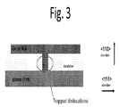
- Still other embodiments not falling within the scope of the invention provide methods for effective ELO of cubic semiconducting materials, as set forth in Fig 3 .
- GaN and other III-N semiconductors have a hexagonal crystal structure. Conditions that favor a high ratio of horizontal to vertical growth rates (GR horizontal / GR vertical ) have not been shown for cubic semiconducting materials such as Ge, or III-V's such as GaAs or InP. This fact makes use of ELO much more difficult.
- a possible solution is to selectively control vertical and horizontal growth rates.
- one may start with a (110)-surface substrate, e.g. silicon (110). An insulator is deposited and patterned thereover. A Ge or III-V cubic material is grown, e.g.
- Embodiments of the invention including the formation of solar cells by the use of ART and ELO are set forth in Fig. 4 .
- the figure 4 shows Ge ART + ELO being used to replace a germanium substrate in a conventional multi-junction configuration.
- a GaAs p/n junction and an InGaP p/n junction are grown on a germanium wafer.
- the InGaP junction has a high band-gap (1.8 eV) and collects the highest energy light
- the GaAs junction (1.4 eV) has a medium-level band-gap and collects the medium energy light.
- the lowest energy light is collected by a germanium p/n junction that is formed on top of the Germanium wafer.
- the conventional configuration may not work well if Ge ART + ELO is used to replace the germanium wafer. There are two reasons for this.
- the germanium cell used in the conventional configuration may be too thick.
- the coefficient of thermal expansion (CTE) of germanium is much different from the coefficient of thermal expansion (CTE) of silicon.
- Germanium grown is typically not stressed at the growth temperature, but is stressed after the cool down. Cracks may form in the germanium to relieve the stress if the germanium is grown too thick.
- the thickness that may lead to cracks is approximately between 5-10 microns; the exact thickness depends on the growth temperature.
- the germanium cell used in the conventional multi-junction configuration is preferably at least 20 microns thick.
- germanium is not a very good absorber of light because the band-gap of germanium is indirect. If the germanium cell is made too thin, much of the light may pass through the germanium cell without being absorbed, which is likely to reduce the efficiency of the cell. This thickness is also required because of current matching: if the germanium cell is too thin, the current that may be produced in the bottom cell may be lower than that which may be produced in the top cell, thereby reducing the current in a series connected device and thus its efficiency.
- the second reason that the conventional configuration may not work well with Ge ART + ELO is because of the high resistance between the germanium and the silicon substrate in this configuration.
- the current can only pass between the germanium and silicon via the narrow trenches that connect the two.
- the oxide that forms the trenches blocks current conduction in the other paths. This high resistance may reduce the efficiency of a solar cell.
- An inverse solar cell may be grown on a Ge ART + ELO substrate as shown in Fig. 5a .
- An GaInP buffer layer may be used between the GaAs and InGaAs to accommodate the difference in the lattice constant between InGaAs and GaAs.
- the InGaAs solar cell may be made quite thin, typically 2 micrometers, because InGaAs is a direct band-gap semiconductor, and therefore absorbs light efficiently.
- the wafer may be flipped over and bonded to a conductive handle wafer.
- the Ge ART + ELO substrate may then be removed by selective etching.
- the selective etching is preferably done very accurately because the silicon substrate, that will be removed, is far thicker than the compound semiconductor solar cell, that is not removed. This selective etching may be accomplished by using a very selective wet etch, such as KOH, which etches silicon quickly but etches germanium very slowly.
- KOH very selective wet etch
- the thin oxide and germanium ART + ELO layers may then be removed in another step, and this step is not nearly as challenging because these layers are not thick relative the compound semiconductor solar cell.
- the InGaAs solar cell that absorbs the low energy light is thin enough to be grown on the Ge ART + ELO substrate without causing cracking.
- the handle wafer provides a low resistance path for the solar cell current.
Landscapes
- Photovoltaic Devices (AREA)
- Recrystallisation Techniques (AREA)
- Life Sciences & Earth Sciences (AREA)
- Engineering & Computer Science (AREA)
- Sustainable Energy (AREA)
- Chemical Vapour Deposition (AREA)
Claims (9)
- Verfahren zum Bilden einer Struktur, wobei das Verfahren die folgenden Schritte umfasst:- Bilden einer ersten Öffnung in einer Maskierungslage, die über einem Substrat angeordnet ist, wobei das Substrat ein erstes Halbleitermaterial umfasst;- Bilden einer zweiten Öffnung in der Maskierungslage;- in der ersten Öffnung und der zweiten Öffnung Bilden einer ersten Lage, die ein zweites Halbleitermaterial umfasst, das gegenüber dem ersten Halbleitermaterial eine Gitterfehlanpassung aufweist, wobei die erste Lage eine Dicke aufweist, die ausreichend ist, damit sie sich über eine obere Oberfläche der Maskierungslage erstreckt;- auf der ersten Lage und über wenigstens einem Teil der Maskierungslage Bilden einer zweiten Lage, die das zweite Halbleitermaterial umfasst, wobei eine vertikale Wachstumsrate der ersten Lage größer als eine seitliche Wachstumsrate der ersten Lage ist und wobei eine seitliche Wachstumsrate der zweiten Lage größer als eine vertikale Wachstumsrate der zweiten Lage ist;- auf der zweiten Lage Bilden einer dritten Lage, die das zweite Halbleitermaterial umfasst, wobei die dritte Lage zwischen der ersten Öffnung und der zweiten Öffnung zusammenwächst, wobei ein Dotieren der dritten Lage ein Facettenwachstum in der dritten Lage verlangsamt und Stapelfehlerbildung in der dritten Lage verringert, und wobei das zweite Halbleitermaterial Germanium und Dotierungen vom p-Typ umfasst;- Bilden einer vierten Lage auf der Oberseite der dritten Lage, wobei die vierte Lage ein drittes Halbleitermaterial umfasst;- Bilden einer fünften Lage auf der Oberseite der vierten Lage, wobei die fünfte Lage ein viertes Halbleitermaterial umfasst;- Bonden der fünften Lage an einen handhabbaren Wafer; und- Entfernen des Substrats,wobei das dritte Halbleitermaterial und das vierte Halbleitermaterial jeweils III-V-Materialien umfassen, wobei das Substrat Silizium umfasst, wobei eine Bandlücke des dritten Halbleitermaterials größer als eine Bandlücke des vierten Halbleitermaterials ist und wobei die Struktur eine Mehrfach-Photovoltaikzelle umfasst.
- Verfahren nach Anspruch 1, wobei die vertikale Wachstumsrate der ersten Lage durch Dotieren der ersten Lage während ihrer Bildung erhöht wird.
- Verfahren nach Anspruch 1, wobei die seitliche Wachstumsrate der ersten Lage durch Dotieren der ersten Lage während ihrer Bildung oder durch Einstellen der Wachstumsparameter verringert wird, um Facetten auf einer Oberseite der ersten Lage während ihrer Bildung zu erzeugen.
- Verfahren nach Anspruch 1, wobei eine Verringerung der vertikalen Wachstumsrate der zweiten Lage ein Dotieren der zweiten Lage während ihrer Bildung oder ein Dotieren der zweiten Lage während ihrer Bildung umfasst, um einen ersten Facettentyp in der zweiten Lage zu bilden und um eine Bildung eines zweiten Facettentyps in der zweiten Lage zu unterdrücken.
- Verfahren nach Anspruch 1, wobei eine Erhöhung der seitlichen Wachstumsrate der zweiten Lage ein Dotieren der zweiten Lage während ihrer Bildung umfasst.
- Verfahren nach Anspruch 1, wobei das Bilden wenigstens der ersten, zweiten oder dritten Lage ein epitaktisches Wachstum umfasst.
- Verfahren nach Anspruch 1, das ferner nach dem Bilden der dritten Lage das Entfernen eines oberen Teils der dritten Lage, um Defekte zu entfernen, und das Bilden einer photonischen Vorrichtung auf der dritten Lage, nachdem der obere Teil entfernt wurde, umfasst.
- Verfahren nach Anspruch 1, wobei ein oberer Teil der ersten Lage eine Facette definiert, die zu einer Oberseite des Substrats nicht parallel ist.
- Verfahren nach Anspruch 1, wobei die dritte Lage selbstplanarisierend ist und wobei die dritte Lage durch Wachsen der dritten Lage vorzugsweise in einer (100)-Richtung selbstplanarisierend ist.
Applications Claiming Priority (4)
| Application Number | Priority Date | Filing Date | Title |
|---|---|---|---|
| US9859708P | 2008-09-19 | 2008-09-19 | |
| US9907408P | 2008-09-22 | 2008-09-22 | |
| US10446608P | 2008-10-10 | 2008-10-10 | |
| EP09815273A EP2335273A4 (de) | 2008-09-19 | 2009-09-18 | Formierung von geräten durch übermässiges wachstum der epitaxialschicht |
Related Parent Applications (2)
| Application Number | Title | Priority Date | Filing Date |
|---|---|---|---|
| EP09815273.9 Division | 2009-09-18 | ||
| EP09815273A Division EP2335273A4 (de) | 2008-09-19 | 2009-09-18 | Formierung von geräten durch übermässiges wachstum der epitaxialschicht |
Publications (3)
| Publication Number | Publication Date |
|---|---|
| EP2528087A2 EP2528087A2 (de) | 2012-11-28 |
| EP2528087A3 EP2528087A3 (de) | 2013-03-20 |
| EP2528087B1 true EP2528087B1 (de) | 2016-06-29 |
Family
ID=42040161
Family Applications (2)
| Application Number | Title | Priority Date | Filing Date |
|---|---|---|---|
| EP12177269.3A Active EP2528087B1 (de) | 2008-09-19 | 2009-09-18 | Formierung von Geräten durch übermässiges Wachstum der Epitaxialschicht |
| EP09815273A Withdrawn EP2335273A4 (de) | 2008-09-19 | 2009-09-18 | Formierung von geräten durch übermässiges wachstum der epitaxialschicht |
Family Applications After (1)
| Application Number | Title | Priority Date | Filing Date |
|---|---|---|---|
| EP09815273A Withdrawn EP2335273A4 (de) | 2008-09-19 | 2009-09-18 | Formierung von geräten durch übermässiges wachstum der epitaxialschicht |
Country Status (6)
| Country | Link |
|---|---|
| US (3) | US8034697B2 (de) |
| EP (2) | EP2528087B1 (de) |
| JP (1) | JP5416212B2 (de) |
| KR (1) | KR101216541B1 (de) |
| CN (1) | CN102160145B (de) |
| WO (1) | WO2010033813A2 (de) |
Families Citing this family (67)
| Publication number | Priority date | Publication date | Assignee | Title |
|---|---|---|---|---|
| US9153645B2 (en) | 2005-05-17 | 2015-10-06 | Taiwan Semiconductor Manufacturing Company, Ltd. | Lattice-mismatched semiconductor structures with reduced dislocation defect densities and related methods for device fabrication |
| US8324660B2 (en) | 2005-05-17 | 2012-12-04 | Taiwan Semiconductor Manufacturing Company, Ltd. | Lattice-mismatched semiconductor structures with reduced dislocation defect densities and related methods for device fabrication |
| US7777250B2 (en) | 2006-03-24 | 2010-08-17 | Taiwan Semiconductor Manufacturing Company, Ltd. | Lattice-mismatched semiconductor structures and related methods for device fabrication |
| US8173551B2 (en) | 2006-09-07 | 2012-05-08 | Taiwan Semiconductor Manufacturing Co., Ltd. | Defect reduction using aspect ratio trapping |
| US7875958B2 (en) | 2006-09-27 | 2011-01-25 | Taiwan Semiconductor Manufacturing Company, Ltd. | Quantum tunneling devices and circuits with lattice-mismatched semiconductor structures |
| US20080187018A1 (en) | 2006-10-19 | 2008-08-07 | Amberwave Systems Corporation | Distributed feedback lasers formed via aspect ratio trapping |
| US9508890B2 (en) | 2007-04-09 | 2016-11-29 | Taiwan Semiconductor Manufacturing Company, Ltd. | Photovoltaics on silicon |
| US8237151B2 (en) | 2009-01-09 | 2012-08-07 | Taiwan Semiconductor Manufacturing Company, Ltd. | Diode-based devices and methods for making the same |
| US7825328B2 (en) | 2007-04-09 | 2010-11-02 | Taiwan Semiconductor Manufacturing Company, Ltd. | Nitride-based multi-junction solar cell modules and methods for making the same |
| US8304805B2 (en) | 2009-01-09 | 2012-11-06 | Taiwan Semiconductor Manufacturing Company, Ltd. | Semiconductor diodes fabricated by aspect ratio trapping with coalesced films |
| US8329541B2 (en) | 2007-06-15 | 2012-12-11 | Taiwan Semiconductor Manufacturing Company, Ltd. | InP-based transistor fabrication |
| JP2010538495A (ja) | 2007-09-07 | 2010-12-09 | アンバーウェーブ・システムズ・コーポレーション | 多接合太陽電池 |
| US8183667B2 (en) | 2008-06-03 | 2012-05-22 | Taiwan Semiconductor Manufacturing Co., Ltd. | Epitaxial growth of crystalline material |
| US8274097B2 (en) | 2008-07-01 | 2012-09-25 | Taiwan Semiconductor Manufacturing Company, Ltd. | Reduction of edge effects from aspect ratio trapping |
| US8981427B2 (en) | 2008-07-15 | 2015-03-17 | Taiwan Semiconductor Manufacturing Company, Ltd. | Polishing of small composite semiconductor materials |
| EP2528087B1 (de) * | 2008-09-19 | 2016-06-29 | Taiwan Semiconductor Manufacturing Company, Ltd. | Formierung von Geräten durch übermässiges Wachstum der Epitaxialschicht |
| US20100072515A1 (en) | 2008-09-19 | 2010-03-25 | Amberwave Systems Corporation | Fabrication and structures of crystalline material |
| US8253211B2 (en) | 2008-09-24 | 2012-08-28 | Taiwan Semiconductor Manufacturing Company, Ltd. | Semiconductor sensor structures with reduced dislocation defect densities |
| JP5705207B2 (ja) | 2009-04-02 | 2015-04-22 | 台湾積體電路製造股▲ふん▼有限公司Taiwan Semiconductor Manufacturing Company,Ltd. | 結晶物質の非極性面から形成される装置とその製作方法 |
| US9484197B2 (en) | 2009-10-23 | 2016-11-01 | The Royal Institution For The Advancement Of Learning/Mcgill University | Lateral growth semiconductor method and devices |
| TWI562195B (en) | 2010-04-27 | 2016-12-11 | Pilegrowth Tech S R L | Dislocation and stress management by mask-less processes using substrate patterning and methods for device fabrication |
| KR101278117B1 (ko) * | 2010-05-20 | 2013-06-24 | 아주대학교산학협력단 | 다중접합 태양전지 및 그 제작방법 |
| US8604330B1 (en) | 2010-12-06 | 2013-12-10 | 4Power, Llc | High-efficiency solar-cell arrays with integrated devices and methods for forming them |
| CN102790006B (zh) * | 2011-05-17 | 2014-09-17 | 中国科学院微电子研究所 | 半导体结构及其制作方法 |
| US8383485B2 (en) | 2011-07-13 | 2013-02-26 | Taiwan Semiconductor Manufacturing Co., Ltd. | Epitaxial process for forming semiconductor devices |
| US8481341B2 (en) * | 2011-11-05 | 2013-07-09 | Tokyo Electron Limited | Epitaxial film growth in retrograde wells for semiconductor devices |
| CN102534768B (zh) * | 2012-02-14 | 2015-03-11 | 中国科学院半导体研究所 | 制备硅基砷化镓材料的方法 |
| EP2629320B1 (de) | 2012-02-15 | 2018-10-17 | IMEC vzw | Maskenstruktur und Verfahren für defektfreie heteroepitaktische Abscheidung |
| US9142400B1 (en) | 2012-07-17 | 2015-09-22 | Stc.Unm | Method of making a heteroepitaxial layer on a seed area |
| US8878251B2 (en) * | 2012-10-17 | 2014-11-04 | Seoul National University R&Db Foundation | Silicon-compatible compound junctionless field effect transistor |
| KR102083495B1 (ko) | 2013-01-07 | 2020-03-02 | 삼성전자 주식회사 | Cmos 소자와 이를 포함하는 광학장치와 그 제조방법 |
| WO2014140082A1 (en) | 2013-03-13 | 2014-09-18 | Pilegrowth Tech S.R.L. | High efficiency solar cells on silicon substrates |
| US8916445B1 (en) | 2013-08-16 | 2014-12-23 | International Business Machines Corporation | Semiconductor devices and methods of manufacture |
| EP2849219A1 (de) | 2013-09-11 | 2015-03-18 | IMEC vzw | Verfahren zur Herstellung von Transistoren und zugehöriges Substrat |
| US9064699B2 (en) | 2013-09-30 | 2015-06-23 | Samsung Electronics Co., Ltd. | Methods of forming semiconductor patterns including reduced dislocation defects and devices formed using such methods |
| KR101464086B1 (ko) * | 2013-10-18 | 2014-11-25 | 희성전자 주식회사 | 다중접합 화합물 태양전지 구조 |
| US9831273B2 (en) | 2013-12-23 | 2017-11-28 | University Of Houston System | Flexible single-crystalline semiconductor device and fabrication methods thereof |
| US9177967B2 (en) * | 2013-12-24 | 2015-11-03 | Intel Corporation | Heterogeneous semiconductor material integration techniques |
| KR102168969B1 (ko) | 2014-02-28 | 2020-10-22 | 삼성전자주식회사 | 반도체 장치 및 그 제조 방법 |
| US9287115B2 (en) | 2014-03-12 | 2016-03-15 | International Business Machines Corporation | Planar III-V field effect transistor (FET) on dielectric layer |
| US9818884B2 (en) | 2014-03-28 | 2017-11-14 | Intel Corporation | Strain compensation in transistors |
| FR3023058B1 (fr) * | 2014-06-30 | 2017-09-29 | Commissariat Energie Atomique | Procede de realisation d'un dispositif microelectronique |
| GB201415119D0 (en) | 2014-08-27 | 2014-10-08 | Ibm | Method for fabricating a semiconductor structure |
| US9711683B2 (en) * | 2014-09-26 | 2017-07-18 | Epistar Corporation | Semiconductor device and the method of manufacturing the same |
| US9349808B2 (en) | 2014-09-29 | 2016-05-24 | International Business Machines Corporation | Double aspect ratio trapping |
| KR102284657B1 (ko) * | 2015-01-05 | 2021-08-02 | 삼성전자 주식회사 | 포토 다이오드 및 이를 포함하는 광통신 시스템 |
| US9564373B2 (en) | 2015-02-27 | 2017-02-07 | International Business Machines Corporation | Forming a CMOS with dual strained channels |
| US9401583B1 (en) | 2015-03-30 | 2016-07-26 | International Business Machines Corporation | Laser structure on silicon using aspect ratio trapping growth |
| US9583599B2 (en) | 2015-04-22 | 2017-02-28 | International Business Machines Corporation | Forming a fin using double trench epitaxy |
| US9633908B2 (en) | 2015-06-16 | 2017-04-25 | International Business Machines Corporation | Method for forming a semiconductor structure containing high mobility semiconductor channel materials |
| US9917414B2 (en) | 2015-07-15 | 2018-03-13 | International Business Machines Corporation | Monolithic nanophotonic device on a semiconductor substrate |
| CN106784127B (zh) * | 2015-11-20 | 2019-02-01 | 北京创昱科技有限公司 | 一种双结薄膜太阳能电池组件及其制作方法 |
| US9704958B1 (en) * | 2015-12-18 | 2017-07-11 | International Business Machines Corporation | III-V field effect transistor on a dielectric layer |
| KR102430501B1 (ko) | 2015-12-29 | 2022-08-09 | 삼성전자주식회사 | 반도체 단결정구조, 반도체 디바이스 및 그 제조방법 |
| US9997475B2 (en) | 2016-01-13 | 2018-06-12 | International Business Machines Corporation | Monolithic integration of III-V cells for powering memory erasure devices |
| FR3047354B1 (fr) * | 2016-01-29 | 2018-05-18 | Commissariat A L'energie Atomique Et Aux Energies Alternatives | Cellule photovoltaique et procede de fabrication d'une cellule photovoltaique |
| US9564452B1 (en) | 2016-02-01 | 2017-02-07 | International Business Machines Corporation | Fabrication of hybrid semiconductor circuits |
| US9704757B1 (en) | 2016-02-25 | 2017-07-11 | International Business Machines Corporation | Fabrication of semiconductor structures |
| US9735010B1 (en) | 2016-05-27 | 2017-08-15 | International Business Machines Corporation | Fabrication of semiconductor fin structures |
| US10249492B2 (en) | 2016-05-27 | 2019-04-02 | International Business Machines Corporation | Fabrication of compound semiconductor structures |
| EP3506000B1 (de) * | 2017-12-29 | 2020-10-07 | IMEC vzw | Iii-v-halbleiterwellenleiter-nanogratstruktur |
| US10777728B2 (en) | 2019-01-18 | 2020-09-15 | Microsoft Technology Licensing, Llc | Fabrication of a quantum device |
| US10978632B2 (en) | 2019-01-18 | 2021-04-13 | Microsoft Technology Licensing, Llc | Fabrication of a device |
| US11742203B2 (en) | 2020-02-26 | 2023-08-29 | The Hong Kong University Of Science And Technology | Method for growing III-V compound semiconductor thin films on silicon-on-insulators |
| TWI864562B (zh) * | 2022-01-27 | 2024-12-01 | 日商京瓷股份有限公司 | 半導體基板之製造方法及製造裝置、以及控制裝置 |
| US20240347561A1 (en) * | 2022-11-10 | 2024-10-17 | The Board Of Trustees Of The University Of Arkansas | Visible to longwave infrared photodetector on silicon |
| EP4656021A2 (de) * | 2023-01-24 | 2025-12-03 | The Regents Of The University Of Michigan | Dickenskalierung einer ferroelektrischen iii-nitrid-schicht |
Citations (1)
| Publication number | Priority date | Publication date | Assignee | Title |
|---|---|---|---|---|
| US20080099785A1 (en) * | 2006-09-07 | 2008-05-01 | Amberwave Systems Coporation | Defect Reduction Using Aspect Ratio Trapping |
Family Cites Families (402)
| Publication number | Priority date | Publication date | Assignee | Title |
|---|---|---|---|---|
| US660928A (en) * | 1900-03-30 | 1900-10-30 | Star And Crescent Mills Company | Heddle mechanism for looms. |
| US4307510A (en) | 1980-03-12 | 1981-12-29 | The United States Of America As Represented By The Administrator Of The National Aeronautics & Space Administration | Computer circuit card puller |
| EP0191505A3 (de) | 1980-04-10 | 1986-09-10 | Massachusetts Institute Of Technology | Verfahren zur Herstellung von Blättern aus kristallinem Material |
| US4322253A (en) | 1980-04-30 | 1982-03-30 | Rca Corporation | Method of making selective crystalline silicon regions containing entrapped hydrogen by laser treatment |
| US4370510A (en) | 1980-09-26 | 1983-01-25 | California Institute Of Technology | Gallium arsenide single crystal solar cell structure and method of making |
| US4651179A (en) | 1983-01-21 | 1987-03-17 | Rca Corporation | Low resistance gallium arsenide field effect transistor |
| US4545109A (en) | 1983-01-21 | 1985-10-08 | Rca Corporation | Method of making a gallium arsenide field effect transistor |
| US5091333A (en) | 1983-09-12 | 1992-02-25 | Massachusetts Institute Of Technology | Reducing dislocations in semiconductors utilizing repeated thermal cycling during multistage epitaxial growth |
| US4860081A (en) | 1984-06-28 | 1989-08-22 | Gte Laboratories Incorporated | Semiconductor integrated circuit structure with insulative partitions |
| US4551394A (en) | 1984-11-26 | 1985-11-05 | Honeywell Inc. | Integrated three-dimensional localized epitaxial growth of Si with localized overgrowth of GaAs |
| EP0214610B1 (de) | 1985-09-03 | 1990-12-05 | Daido Tokushuko Kabushiki Kaisha | Epitaktische Gallium-Arsenid-Halbleiterscheibe und Verfahren zu ihrer Herstellung |
| US4774205A (en) | 1986-06-13 | 1988-09-27 | Massachusetts Institute Of Technology | Monolithic integration of silicon and gallium arsenide devices |
| JPS6381855A (ja) | 1986-09-25 | 1988-04-12 | Mitsubishi Electric Corp | ヘテロ接合バイポ−ラトランジスタの製造方法 |
| US5269876A (en) | 1987-01-26 | 1993-12-14 | Canon Kabushiki Kaisha | Process for producing crystal article |
| US5236546A (en) | 1987-01-26 | 1993-08-17 | Canon Kabushiki Kaisha | Process for producing crystal article |
| US5281283A (en) | 1987-03-26 | 1994-01-25 | Canon Kabushiki Kaisha | Group III-V compound crystal article using selective epitaxial growth |
| US5166767A (en) | 1987-04-14 | 1992-11-24 | National Semiconductor Corporation | Sidewall contact bipolar transistor with controlled lateral spread of selectively grown epitaxial layer |
| US4876210A (en) | 1987-04-30 | 1989-10-24 | The University Of Delaware | Solution growth of lattice mismatched and solubility mismatched heterostructures |
| US4826784A (en) | 1987-11-13 | 1989-05-02 | Kopin Corporation | Selective OMCVD growth of compound semiconductor materials on silicon substrates |
| US5079616A (en) | 1988-02-11 | 1992-01-07 | Gte Laboratories Incorporated | Semiconductor structure |
| US5272105A (en) | 1988-02-11 | 1993-12-21 | Gte Laboratories Incorporated | Method of manufacturing an heteroepitaxial semiconductor structure |
| GB2215514A (en) | 1988-03-04 | 1989-09-20 | Plessey Co Plc | Terminating dislocations in semiconductor epitaxial layers |
| US5032893A (en) | 1988-04-01 | 1991-07-16 | Cornell Research Foundation, Inc. | Method for reducing or eliminating interface defects in mismatched semiconductor eiplayers |
| US5156995A (en) | 1988-04-01 | 1992-10-20 | Cornell Research Foundation, Inc. | Method for reducing or eliminating interface defects in mismatched semiconductor epilayers |
| US5238869A (en) | 1988-07-25 | 1993-08-24 | Texas Instruments Incorporated | Method of forming an epitaxial layer on a heterointerface |
| EP0352472A3 (de) | 1988-07-25 | 1991-02-06 | Texas Instruments Incorporated | Heteroepitaxie von Halbleitermaterialien mit ungleichen Gittern |
| JPH0262090A (ja) | 1988-08-29 | 1990-03-01 | Matsushita Electric Ind Co Ltd | 光半導体装置の製造方法 |
| US5061644A (en) | 1988-12-22 | 1991-10-29 | Honeywell Inc. | Method for fabricating self-aligned semiconductor devices |
| EP0380815B1 (de) | 1989-01-31 | 1994-05-25 | Agfa-Gevaert N.V. | Integration von GaAs auf Si-Unterlage |
| US5034337A (en) | 1989-02-10 | 1991-07-23 | Texas Instruments Incorporated | Method of making an integrated circuit that combines multi-epitaxial power transistors with logic/analog devices |
| US4948456A (en) | 1989-06-09 | 1990-08-14 | Delco Electronics Corporation | Confined lateral selective epitaxial growth |
| US5098850A (en) | 1989-06-16 | 1992-03-24 | Canon Kabushiki Kaisha | Process for producing substrate for selective crystal growth, selective crystal growth process and process for producing solar battery by use of them |
| US5256594A (en) | 1989-06-16 | 1993-10-26 | Intel Corporation | Masking technique for depositing gallium arsenide on silicon |
| US5093699A (en) | 1990-03-12 | 1992-03-03 | Texas A & M University System | Gate adjusted resonant tunnel diode device and method of manufacture |
| US5164359A (en) | 1990-04-20 | 1992-11-17 | Eaton Corporation | Monolithic integrated circuit having compound semiconductor layer epitaxially grown on ceramic substrate |
| US5158907A (en) | 1990-08-02 | 1992-10-27 | At&T Bell Laboratories | Method for making semiconductor devices with low dislocation defects |
| US5105247A (en) | 1990-08-03 | 1992-04-14 | Cavanaugh Marion E | Quantum field effect device with source extension region formed under a gate and between the source and drain regions |
| JP3202223B2 (ja) | 1990-11-27 | 2001-08-27 | 日本電気株式会社 | トランジスタの製造方法 |
| US5403751A (en) | 1990-11-29 | 1995-04-04 | Canon Kabushiki Kaisha | Process for producing a thin silicon solar cell |
| US5223043A (en) | 1991-02-11 | 1993-06-29 | The United States Of America As Represented By The United States Department Of Energy | Current-matched high-efficiency, multijunction monolithic solar cells |
| US5091767A (en) | 1991-03-18 | 1992-02-25 | At&T Bell Laboratories | Article comprising a lattice-mismatched semiconductor heterostructure |
| JPH04299569A (ja) | 1991-03-27 | 1992-10-22 | Nec Corp | Soisの製造方法及びトランジスタとその製造方法 |
| US5269852A (en) | 1991-05-27 | 1993-12-14 | Canon Kabushiki Kaisha | Crystalline solar cell and method for producing the same |
| JP3058954B2 (ja) | 1991-09-24 | 2000-07-04 | ローム株式会社 | 絶縁層の上に成長層を有する半導体装置の製造方法 |
| JP2773487B2 (ja) | 1991-10-15 | 1998-07-09 | 日本電気株式会社 | トンネルトランジスタ |
| JPH05121317A (ja) | 1991-10-24 | 1993-05-18 | Rohm Co Ltd | Soi構造形成方法 |
| JP3286920B2 (ja) | 1992-07-10 | 2002-05-27 | 富士通株式会社 | 半導体装置の製造方法 |
| DE59308841D1 (de) | 1992-12-04 | 1998-09-10 | Siemens Ag | Verfahren zur Herstellung eines seitlich begrenzten, einkristallinen Gebietes mittels selektiver Epitaxie und dessen Anwendung zur Herstellung eines Bipolartransistors sowie eines MOS-transistors |
| JP3319472B2 (ja) | 1992-12-07 | 2002-09-03 | 富士通株式会社 | 半導体装置とその製造方法 |
| US5295150A (en) | 1992-12-11 | 1994-03-15 | Eastman Kodak Company | Distributed feedback-channeled substrate planar semiconductor laser |
| US5407491A (en) | 1993-04-08 | 1995-04-18 | University Of Houston | Tandem solar cell with improved tunnel junction |
| EP0627799B1 (de) | 1993-06-04 | 1997-10-08 | Sharp Kabushiki Kaisha | Lichtmittierende Halbleitervorrichtung mit einer dritten Begrenzungsschicht |
| JP3748905B2 (ja) | 1993-08-27 | 2006-02-22 | 三洋電機株式会社 | 量子効果デバイス |
| US5792679A (en) | 1993-08-30 | 1998-08-11 | Sharp Microelectronics Technology, Inc. | Method for forming silicon-germanium/Si/silicon dioxide heterostructure using germanium implant |
| US5461243A (en) | 1993-10-29 | 1995-10-24 | International Business Machines Corporation | Substrate for tensilely strained semiconductor |
| US5405453A (en) | 1993-11-08 | 1995-04-11 | Applied Solar Energy Corporation | High efficiency multi-junction solar cell |
| US5489539A (en) | 1994-01-10 | 1996-02-06 | Hughes Aircraft Company | Method of making quantum well structure with self-aligned gate |
| JPH07230952A (ja) | 1994-02-16 | 1995-08-29 | Ricoh Co Ltd | 再結晶化方法 |
| JPH0851109A (ja) | 1994-04-11 | 1996-02-20 | Texas Instr Inc <Ti> | 酸化物でパターン化されたウェーハの窓内にエピタキシャルシリコンを成長させる方法 |
| US6011271A (en) | 1994-04-28 | 2000-01-04 | Fujitsu Limited | Semiconductor device and method of fabricating the same |
| US5710436A (en) | 1994-09-27 | 1998-01-20 | Kabushiki Kaisha Toshiba | Quantum effect device |
| US5825240A (en) | 1994-11-30 | 1998-10-20 | Massachusetts Institute Of Technology | Resonant-tunneling transmission line technology |
| JP3835225B2 (ja) | 1995-02-23 | 2006-10-18 | 日亜化学工業株式会社 | 窒化物半導体発光素子 |
| US5528209A (en) | 1995-04-27 | 1996-06-18 | Hughes Aircraft Company | Monolithic microwave integrated circuit and method |
| JPH08306700A (ja) | 1995-04-27 | 1996-11-22 | Nec Corp | 半導体装置及びその製造方法 |
| TW304310B (de) | 1995-05-31 | 1997-05-01 | Siemens Ag | |
| US5621227A (en) | 1995-07-18 | 1997-04-15 | Discovery Semiconductors, Inc. | Method and apparatus for monolithic optoelectronic integrated circuit using selective epitaxy |
| JPH11500873A (ja) | 1995-12-15 | 1999-01-19 | フィリップス エレクトロニクス ネムローゼ フェンノートシャップ | SiGe層を具えた半導体電界効果デバイス |
| TW314621B (de) | 1995-12-20 | 1997-09-01 | Toshiba Co Ltd | |
| US5987590A (en) | 1996-04-02 | 1999-11-16 | Texas Instruments Incorporated | PC circuits, systems and methods |
| EP0807980B1 (de) | 1996-05-17 | 2006-06-21 | Canon Kabushiki Kaisha | Photovoltaische Anordnung und Herstellungsverfahren |
| JP3719618B2 (ja) | 1996-06-17 | 2005-11-24 | 松下電器産業株式会社 | 半導体装置及びその製造方法 |
| US6229153B1 (en) | 1996-06-21 | 2001-05-08 | Wisconsin Alumni Research Corporation | High peak current density resonant tunneling diode |
| JP3260660B2 (ja) | 1996-08-22 | 2002-02-25 | 株式会社東芝 | 半導体装置およびその製造方法 |
| JP3449516B2 (ja) | 1996-08-30 | 2003-09-22 | 株式会社リコー | 半導体多層膜反射鏡および半導体多層膜反射防止膜および面発光型半導体レーザおよび受光素子 |
| US6191432B1 (en) | 1996-09-02 | 2001-02-20 | Kabushiki Kaisha Toshiba | Semiconductor device and memory device |
| US5825049A (en) | 1996-10-09 | 1998-10-20 | Sandia Corporation | Resonant tunneling device with two-dimensional quantum well emitter and base layers |
| JPH10126010A (ja) | 1996-10-23 | 1998-05-15 | Ricoh Co Ltd | 半導体レーザ装置の製造方法 |
| SG65697A1 (en) | 1996-11-15 | 1999-06-22 | Canon Kk | Process for producing semiconductor article |
| US5853497A (en) | 1996-12-12 | 1998-12-29 | Hughes Electronics Corporation | High efficiency multi-junction solar cells |
| US6348096B1 (en) | 1997-03-13 | 2002-02-19 | Nec Corporation | Method for manufacturing group III-V compound semiconductors |
| JP3853905B2 (ja) | 1997-03-18 | 2006-12-06 | 株式会社東芝 | 量子効果装置とblトンネル素子を用いた装置 |
| EP0874405A3 (de) | 1997-03-25 | 2004-09-15 | Mitsubishi Cable Industries, Ltd. | Element auf Basis von GaN mit niedriger Versetzungsdichte, seine Verwendung und Herstellungsverfahren |
| CN1131548C (zh) | 1997-04-04 | 2003-12-17 | 松下电器产业株式会社 | 半导体装置 |
| JP3047852B2 (ja) | 1997-04-04 | 2000-06-05 | 松下電器産業株式会社 | 半導体装置 |
| JP3184115B2 (ja) | 1997-04-11 | 2001-07-09 | 松下電器産業株式会社 | オーミック電極形成方法 |
| EP2234142A1 (de) | 1997-04-11 | 2010-09-29 | Nichia Corporation | Nitridhalbleitersubstrat |
| US5998781A (en) | 1997-04-30 | 1999-12-07 | Sandia Corporation | Apparatus for millimeter-wave signal generation |
| US5903170A (en) | 1997-06-03 | 1999-05-11 | The Regents Of The University Of Michigan | Digital logic design using negative differential resistance diodes and field-effect transistors |
| US5883549A (en) | 1997-06-20 | 1999-03-16 | Hughes Electronics Corporation | Bipolar junction transistor (BJT)--resonant tunneling diode (RTD) oscillator circuit and method |
| EP1016129B2 (de) | 1997-06-24 | 2009-06-10 | Massachusetts Institute Of Technology | Kontrolle der verspannungsdichte durch verwendung von gradientenschichten und durch planarisierung |
| US5869845A (en) | 1997-06-26 | 1999-02-09 | Texas Instruments Incorporated | Resonant tunneling memory |
| US6015979A (en) | 1997-08-29 | 2000-01-18 | Kabushiki Kaisha Toshiba | Nitride-based semiconductor element and method for manufacturing the same |
| JP3930161B2 (ja) | 1997-08-29 | 2007-06-13 | 株式会社東芝 | 窒化物系半導体素子、発光素子及びその製造方法 |
| CA2302758A1 (en) | 1997-09-16 | 1999-03-25 | Eugene A. Fitzgerald | Co-planar si and ge composite substrate and method of producing same |
| FR2769924B1 (fr) | 1997-10-20 | 2000-03-10 | Centre Nat Rech Scient | Procede de realisation d'une couche epitaxiale de nitrure de gallium, couche epitaxiale de nitrure de gallium et composant optoelectronique muni d'une telle couche |
| JP5065625B2 (ja) * | 1997-10-30 | 2012-11-07 | 住友電気工業株式会社 | GaN単結晶基板の製造方法 |
| EP1041610B1 (de) | 1997-10-30 | 2010-12-15 | Sumitomo Electric Industries, Ltd. | Gan einkristall-substrat und herstellungsmethode |
| JP3180743B2 (ja) | 1997-11-17 | 2001-06-25 | 日本電気株式会社 | 窒化化合物半導体発光素子およびその製法 |
| JP3468082B2 (ja) | 1998-02-26 | 2003-11-17 | 日亜化学工業株式会社 | 窒化物半導体素子 |
| US6150242A (en) | 1998-03-25 | 2000-11-21 | Texas Instruments Incorporated | Method of growing crystalline silicon overlayers on thin amorphous silicon oxide layers and forming by method a resonant tunneling diode |
| JPH11274467A (ja) | 1998-03-26 | 1999-10-08 | Murata Mfg Co Ltd | 光電子集積回路素子 |
| US6500257B1 (en) | 1998-04-17 | 2002-12-31 | Agilent Technologies, Inc. | Epitaxial material grown laterally within a trench and method for producing same |
| JP3338778B2 (ja) | 1998-04-24 | 2002-10-28 | 日本電気株式会社 | 窒化物系化合物半導体レーザ素子 |
| US6265289B1 (en) | 1998-06-10 | 2001-07-24 | North Carolina State University | Methods of fabricating gallium nitride semiconductor layers by lateral growth from sidewalls into trenches, and gallium nitride semiconductor structures fabricated thereby |
| TW417315B (en) * | 1998-06-18 | 2001-01-01 | Sumitomo Electric Industries | GaN single crystal substrate and its manufacture method of the same |
| JP4005701B2 (ja) | 1998-06-24 | 2007-11-14 | シャープ株式会社 | 窒素化合物半導体膜の形成方法および窒素化合物半導体素子 |
| US6606335B1 (en) | 1998-07-14 | 2003-08-12 | Fujitsu Limited | Semiconductor laser, semiconductor device, and their manufacture methods |
| EP1115163A4 (de) | 1998-09-10 | 2001-12-05 | Rohm Co Ltd | Halbleiter lichtemittierende vorrichtung und herstellungsverfahren |
| US6252261B1 (en) | 1998-09-30 | 2001-06-26 | Nec Corporation | GaN crystal film, a group III element nitride semiconductor wafer and a manufacturing process therefor |
| US6255198B1 (en) * | 1998-11-24 | 2001-07-03 | North Carolina State University | Methods of fabricating gallium nitride microelectronic layers on silicon layers and gallium nitride microelectronic structures formed thereby |
| JP3868136B2 (ja) | 1999-01-20 | 2007-01-17 | 日亜化学工業株式会社 | 窒化ガリウム系化合物半導体発光素子 |
| JP3372226B2 (ja) | 1999-02-10 | 2003-01-27 | 日亜化学工業株式会社 | 窒化物半導体レーザ素子 |
| US7145167B1 (en) | 2000-03-11 | 2006-12-05 | International Business Machines Corporation | High speed Ge channel heterostructures for field effect devices |
| JP3760663B2 (ja) | 1999-03-31 | 2006-03-29 | 豊田合成株式会社 | Iii族窒化物系化合物半導体素子の製造方法 |
| JP3702700B2 (ja) | 1999-03-31 | 2005-10-05 | 豊田合成株式会社 | Iii族窒化物系化合物半導体素子及びその製造方法 |
| DE10017137A1 (de) | 1999-04-14 | 2000-10-26 | Siemens Ag | Silizium-Aufbau und Verfahren zu dessen Herstellung |
| US6803598B1 (en) | 1999-05-07 | 2004-10-12 | University Of Delaware | Si-based resonant interband tunneling diodes and method of making interband tunneling diodes |
| JP3587081B2 (ja) | 1999-05-10 | 2004-11-10 | 豊田合成株式会社 | Iii族窒化物半導体の製造方法及びiii族窒化物半導体発光素子 |
| JP4246400B2 (ja) | 1999-05-13 | 2009-04-02 | 株式会社日立製作所 | 半導体記憶装置 |
| US6252287B1 (en) | 1999-05-19 | 2001-06-26 | Sandia Corporation | InGaAsN/GaAs heterojunction for multi-junction solar cells |
| JP3555500B2 (ja) | 1999-05-21 | 2004-08-18 | 豊田合成株式会社 | Iii族窒化物半導体及びその製造方法 |
| GB9912178D0 (en) | 1999-05-25 | 1999-07-28 | Univ Court Of The University O | Improved optical modulator |
| US6214653B1 (en) | 1999-06-04 | 2001-04-10 | International Business Machines Corporation | Method for fabricating complementary metal oxide semiconductor (CMOS) devices on a mixed bulk and silicon-on-insulator (SOI) substrate |
| JP2001007447A (ja) | 1999-06-18 | 2001-01-12 | Nichia Chem Ind Ltd | 窒化物半導体レーザ素子 |
| US6635110B1 (en) | 1999-06-25 | 2003-10-21 | Massachusetts Institute Of Technology | Cyclic thermal anneal for dislocation reduction |
| US6228691B1 (en) | 1999-06-30 | 2001-05-08 | Intel Corp. | Silicon-on-insulator devices and method for producing the same |
| GB9919479D0 (en) | 1999-08-17 | 1999-10-20 | Imperial College | Island arrays |
| US6339232B1 (en) | 1999-09-20 | 2002-01-15 | Kabushika Kaisha Toshiba | Semiconductor device |
| JP2001102678A (ja) | 1999-09-29 | 2001-04-13 | Toshiba Corp | 窒化ガリウム系化合物半導体素子 |
| US6984571B1 (en) | 1999-10-01 | 2006-01-10 | Ziptronix, Inc. | Three dimensional device integration method and integrated device |
| US6812053B1 (en) | 1999-10-14 | 2004-11-02 | Cree, Inc. | Single step pendeo- and lateral epitaxial overgrowth of Group III-nitride epitaxial layers with Group III-nitride buffer layer and resulting structures |
| JP2001189483A (ja) | 1999-10-18 | 2001-07-10 | Sharp Corp | バイパス機能付太陽電池セルおよびバイパス機能付き多接合積層型太陽電池セルおよびそれらの製造方法 |
| EP1102327B1 (de) | 1999-11-15 | 2007-10-03 | Matsushita Electric Industrial Co., Ltd. | Feldeffekt-Halbleiterbauelement |
| US6521514B1 (en) | 1999-11-17 | 2003-02-18 | North Carolina State University | Pendeoepitaxial methods of fabricating gallium nitride semiconductor layers on sapphire substrates |
| JP2001176805A (ja) | 1999-12-16 | 2001-06-29 | Sony Corp | 窒化物系iii−v族化合物の結晶製造方法、窒化物系iii−v族化合物結晶基板、窒化物系iii−v族化合物結晶膜およびデバイスの製造方法 |
| US6403451B1 (en) | 2000-02-09 | 2002-06-11 | Noerh Carolina State University | Methods of fabricating gallium nitride semiconductor layers on substrates including non-gallium nitride posts |
| WO2001058383A2 (en) | 2000-02-11 | 2001-08-16 | Novo Rps Ulc | Stent delivery system and method of use |
| US6902987B1 (en) | 2000-02-16 | 2005-06-07 | Ziptronix, Inc. | Method for low temperature bonding and bonded structure |
| JP3512701B2 (ja) | 2000-03-10 | 2004-03-31 | 株式会社東芝 | 半導体装置及びその製造方法 |
| TW504754B (en) | 2000-03-24 | 2002-10-01 | Sumitomo Chemical Co | Group III-V compound semiconductor and method of producing the same |
| US20050184302A1 (en) | 2000-04-04 | 2005-08-25 | Toshimasa Kobayashi | Nitride semiconductor device and method of manufacturing the same |
| US6362071B1 (en) | 2000-04-05 | 2002-03-26 | Motorola, Inc. | Method for forming a semiconductor device with an opening in a dielectric layer |
| JP2001338988A (ja) | 2000-05-25 | 2001-12-07 | Hitachi Ltd | 半導体装置及びその製造方法 |
| US6627974B2 (en) * | 2000-06-19 | 2003-09-30 | Nichia Corporation | Nitride semiconductor substrate and method for manufacturing the same, and nitride semiconductor device using nitride semiconductor substrate |
| US6841808B2 (en) | 2000-06-23 | 2005-01-11 | Toyoda Gosei Co., Ltd. | Group III nitride compound semiconductor device and method for producing the same |
| US20020008234A1 (en) | 2000-06-28 | 2002-01-24 | Motorola, Inc. | Mixed-signal semiconductor structure, device including the structure, and methods of forming the device and the structure |
| US20020030246A1 (en) | 2000-06-28 | 2002-03-14 | Motorola, Inc. | Structure and method for fabricating semiconductor structures and devices not lattice matched to the substrate |
| US7906229B2 (en) * | 2007-03-08 | 2011-03-15 | Amit Goyal | Semiconductor-based, large-area, flexible, electronic devices |
| WO2002009187A2 (en) | 2000-07-24 | 2002-01-31 | Motorola, Inc. | Heterojunction tunneling diodes and process for fabricating same |
| US20020011612A1 (en) | 2000-07-31 | 2002-01-31 | Kabushiki Kaisha Toshiba | Semiconductor device and method for manufacturing the same |
| JP2002118255A (ja) | 2000-07-31 | 2002-04-19 | Toshiba Corp | 半導体装置およびその製造方法 |
| JP4269541B2 (ja) | 2000-08-01 | 2009-05-27 | 株式会社Sumco | 半導体基板と電界効果型トランジスタ並びにSiGe層の形成方法及びこれを用いた歪みSi層の形成方法と電界効果型トランジスタの製造方法 |
| US6579463B1 (en) | 2000-08-18 | 2003-06-17 | The Regents Of The University Of Colorado | Tunable nanomasks for pattern transfer and nanocluster array formation |
| US20060175601A1 (en) | 2000-08-22 | 2006-08-10 | President And Fellows Of Harvard College | Nanoscale wires and related devices |
| US7301199B2 (en) | 2000-08-22 | 2007-11-27 | President And Fellows Of Harvard College | Nanoscale wires and related devices |
| US6407425B1 (en) | 2000-09-21 | 2002-06-18 | Texas Instruments Incorporated | Programmable neuron MOSFET on SOI |
| US6456214B1 (en) | 2000-09-27 | 2002-09-24 | Raytheon Company | High-speed comparator utilizing resonant tunneling diodes and associated method |
| JP4044276B2 (ja) | 2000-09-28 | 2008-02-06 | 株式会社東芝 | 半導体装置及びその製造方法 |
| US7163864B1 (en) | 2000-10-18 | 2007-01-16 | International Business Machines Corporation | Method of fabricating semiconductor side wall fin |
| US6720090B2 (en) | 2001-01-02 | 2004-04-13 | Eastman Kodak Company | Organic light emitting diode devices with improved luminance efficiency |
| US6594293B1 (en) * | 2001-02-08 | 2003-07-15 | Amberwave Systems Corporation | Relaxed InxGa1-xAs layers integrated with Si |
| EP1367150B1 (de) | 2001-02-14 | 2009-08-19 | Toyoda Gosei Co., Ltd. | Verfahren zur herstellung von halbleiterkristallen und halbleiter-leuchtelementen |
| JP4084541B2 (ja) | 2001-02-14 | 2008-04-30 | 豊田合成株式会社 | 半導体結晶及び半導体発光素子の製造方法 |
| JP4084544B2 (ja) | 2001-03-30 | 2008-04-30 | 豊田合成株式会社 | 半導体基板及び半導体素子の製造方法 |
| US6380590B1 (en) | 2001-02-22 | 2002-04-30 | Advanced Micro Devices, Inc. | SOI chip having multiple threshold voltage MOSFETs by using multiple channel materials and method of fabricating same |
| US6475869B1 (en) | 2001-02-26 | 2002-11-05 | Advanced Micro Devices, Inc. | Method of forming a double gate transistor having an epitaxial silicon/germanium channel region |
| JP3679720B2 (ja) | 2001-02-27 | 2005-08-03 | 三洋電機株式会社 | 窒化物系半導体素子および窒化物系半導体の形成方法 |
| JP2002270516A (ja) | 2001-03-07 | 2002-09-20 | Nec Corp | Iii族窒化物半導体の成長方法、iii族窒化物半導体膜およびそれを用いた半導体素子 |
| US7205604B2 (en) | 2001-03-13 | 2007-04-17 | International Business Machines Corporation | Ultra scalable high speed heterojunction vertical n-channel MISFETs and methods thereof |
| JP3705142B2 (ja) | 2001-03-27 | 2005-10-12 | ソニー株式会社 | 窒化物半導体素子及びその作製方法 |
| KR20040000418A (ko) | 2001-03-30 | 2004-01-03 | 더 리전트 오브 더 유니버시티 오브 캘리포니아 | 나노구조체 및 나노와이어의 제조 방법 및 그로부터제조되는 디바이스 |
| JP3956637B2 (ja) | 2001-04-12 | 2007-08-08 | ソニー株式会社 | 窒化物半導体の結晶成長方法及び半導体素子の形成方法 |
| GB0110112D0 (en) | 2001-04-25 | 2001-06-20 | Univ Glasgow | Improved optoelectronic device |
| GB0111207D0 (en) | 2001-05-08 | 2001-06-27 | Btg Int Ltd | A method to produce germanium layers |
| US6784074B2 (en) | 2001-05-09 | 2004-08-31 | Nsc-Nanosemiconductor Gmbh | Defect-free semiconductor templates for epitaxial growth and method of making same |
| JP3819730B2 (ja) | 2001-05-11 | 2006-09-13 | 三洋電機株式会社 | 窒化物系半導体素子および窒化物半導体の形成方法 |
| US20020168802A1 (en) | 2001-05-14 | 2002-11-14 | Hsu Sheng Teng | SiGe/SOI CMOS and method of making the same |
| US7358578B2 (en) | 2001-05-22 | 2008-04-15 | Renesas Technology Corporation | Field effect transistor on a substrate with (111) orientation having zirconium oxide gate insulation and cobalt or nickel silicide wiring |
| JP3515974B2 (ja) | 2001-06-13 | 2004-04-05 | 松下電器産業株式会社 | 窒化物半導体、その製造方法及び窒化物半導体素子 |
| TW544956B (en) | 2001-06-13 | 2003-08-01 | Matsushita Electric Industrial Co Ltd | Nitride semiconductor, production method therefor and nitride semiconductor element |
| US6566284B2 (en) | 2001-08-07 | 2003-05-20 | Hrl Laboratories, Llc | Method of manufacture for 80 nanometer diameter resonant tunneling diode with improved peak-to-valley ratio and resonant tunneling diode therefrom |
| JP3785970B2 (ja) | 2001-09-03 | 2006-06-14 | 日本電気株式会社 | Iii族窒化物半導体素子の製造方法 |
| JP2003077847A (ja) | 2001-09-06 | 2003-03-14 | Sumitomo Chem Co Ltd | 3−5族化合物半導体の製造方法 |
| TW544930B (en) | 2001-09-11 | 2003-08-01 | Toyoda Gosei Kk | Method for producing semiconductor crystal |
| JP2003163370A (ja) | 2001-09-11 | 2003-06-06 | Toyoda Gosei Co Ltd | 半導体結晶の製造方法 |
| US7105865B2 (en) | 2001-09-19 | 2006-09-12 | Sumitomo Electric Industries, Ltd. | AlxInyGa1−x−yN mixture crystal substrate |
| US6689650B2 (en) | 2001-09-27 | 2004-02-10 | International Business Machines Corporation | Fin field effect transistor with self-aligned gate |
| US20030064535A1 (en) | 2001-09-28 | 2003-04-03 | Kub Francis J. | Method of manufacturing a semiconductor device having a thin GaN material directly bonded to an optimized substrate |
| US6710368B2 (en) | 2001-10-01 | 2004-03-23 | Ken Scott Fisher | Quantum tunneling transistor |
| US20030070707A1 (en) | 2001-10-12 | 2003-04-17 | King Richard Roland | Wide-bandgap, lattice-mismatched window layer for a solar energy conversion device |
| JP2003142728A (ja) | 2001-11-02 | 2003-05-16 | Sharp Corp | 半導体発光素子の製造方法 |
| JP2003152220A (ja) | 2001-11-15 | 2003-05-23 | Sharp Corp | 半導体発光素子の製造方法および半導体発光素子 |
| US6835246B2 (en) | 2001-11-16 | 2004-12-28 | Saleem H. Zaidi | Nanostructures for hetero-expitaxial growth on silicon substrates |
| US6576532B1 (en) | 2001-11-30 | 2003-06-10 | Motorola Inc. | Semiconductor device and method therefor |
| JP4284188B2 (ja) | 2001-12-20 | 2009-06-24 | パナソニック株式会社 | 窒化物系半導体基板の製造方法および窒化物系半導体装置の製造方法 |
| EP2262007B1 (de) | 2002-01-28 | 2016-11-23 | Nichia Corporation | Nitrid-Halbleiterelement mit Trägersubstrat |
| KR100458288B1 (ko) | 2002-01-30 | 2004-11-26 | 한국과학기술원 | 이중-게이트 FinFET 소자 및 그 제조방법 |
| US7411233B2 (en) | 2002-08-27 | 2008-08-12 | E-Phocus, Inc | Photoconductor-on-active-pixel (POAP) sensor utilizing a multi-layered radiation absorbing structure |
| US6492216B1 (en) | 2002-02-07 | 2002-12-10 | Taiwan Semiconductor Manufacturing Company | Method of forming a transistor with a strained channel |
| JP3782021B2 (ja) | 2002-02-22 | 2006-06-07 | 株式会社東芝 | 半導体装置、半導体装置の製造方法、半導体基板の製造方法 |
| AU2002252110A1 (en) | 2002-02-27 | 2003-09-09 | Midwest Research Institute | Monolithic photovoltaic energy conversion device |
| JP4092927B2 (ja) | 2002-02-28 | 2008-05-28 | 豊田合成株式会社 | Iii族窒化物系化合物半導体、iii族窒化物系化合物半導体素子及びiii族窒化物系化合物半導体基板の製造方法 |
| US6635909B2 (en) | 2002-03-19 | 2003-10-21 | International Business Machines Corporation | Strained fin FETs structure and method |
| KR101288489B1 (ko) | 2002-04-15 | 2013-07-26 | 더 리전츠 오브 더 유니버시티 오브 캘리포니아 | 무극성 질화(알루미늄, 붕소, 인듐, 갈륨) 양자우물 및이형구조 재료 및 장치 |
| US7208393B2 (en) | 2002-04-15 | 2007-04-24 | The Regents Of The University Of California | Growth of planar reduced dislocation density m-plane gallium nitride by hydride vapor phase epitaxy |
| US8067687B2 (en) | 2002-05-21 | 2011-11-29 | Alliance For Sustainable Energy, Llc | High-efficiency, monolithic, multi-bandgap, tandem photovoltaic energy converters |
| US20060162768A1 (en) | 2002-05-21 | 2006-07-27 | Wanlass Mark W | Low bandgap, monolithic, multi-bandgap, optoelectronic devices |
| US7217882B2 (en) | 2002-05-24 | 2007-05-15 | Cornell Research Foundation, Inc. | Broad spectrum solar cell |
| CN2550906Y (zh) | 2002-05-27 | 2003-05-14 | 李映华 | 立体光双面结光电池 |
| FR2840452B1 (fr) | 2002-05-28 | 2005-10-14 | Lumilog | Procede de realisation par epitaxie d'un film de nitrure de gallium separe de son substrat |
| TWI271877B (en) | 2002-06-04 | 2007-01-21 | Nitride Semiconductors Co Ltd | Gallium nitride compound semiconductor device and manufacturing method |
| JP2004014856A (ja) | 2002-06-07 | 2004-01-15 | Sharp Corp | 半導体基板の製造方法及び半導体装置の製造方法 |
| US7074623B2 (en) | 2002-06-07 | 2006-07-11 | Amberwave Systems Corporation | Methods of forming strained-semiconductor-on-insulator finFET device structures |
| US6995430B2 (en) | 2002-06-07 | 2006-02-07 | Amberwave Systems Corporation | Strained-semiconductor-on-insulator device structures |
| US6887773B2 (en) | 2002-06-19 | 2005-05-03 | Luxtera, Inc. | Methods of incorporating germanium within CMOS process |
| WO2004001857A1 (en) | 2002-06-19 | 2003-12-31 | Massachusetts Institute Of Technology | Ge photodetectors |
| US7012298B1 (en) | 2002-06-21 | 2006-03-14 | Advanced Micro Devices, Inc. | Non-volatile memory device |
| US6617643B1 (en) | 2002-06-28 | 2003-09-09 | Mcnc | Low power tunneling metal-oxide-semiconductor (MOS) device |
| US7335908B2 (en) | 2002-07-08 | 2008-02-26 | Qunano Ab | Nanostructures and methods for manufacturing the same |
| US6982204B2 (en) | 2002-07-16 | 2006-01-03 | Cree, Inc. | Nitride-based transistors and methods of fabrication thereof using non-etched contact recesses |
| US20040012037A1 (en) | 2002-07-18 | 2004-01-22 | Motorola, Inc. | Hetero-integration of semiconductor materials on silicon |
| EP2267762A3 (de) * | 2002-08-23 | 2012-08-22 | Taiwan Semiconductor Manufacturing Co., Ltd. | Halbleiter-Heterostrukturen mit reduzierter Anhäufung von Versetzungen und entsprechende Herstellungsverfahren |
| US7015497B1 (en) | 2002-08-27 | 2006-03-21 | The Ohio State University | Self-aligned and self-limited quantum dot nanoswitches and methods for making same |
| US20040043584A1 (en) | 2002-08-27 | 2004-03-04 | Thomas Shawn G. | Semiconductor device and method of making same |
| GB0220438D0 (en) | 2002-09-03 | 2002-10-09 | Univ Warwick | Formation of lattice-turning semiconductor substrates |
| US7122733B2 (en) | 2002-09-06 | 2006-10-17 | The Boeing Company | Multi-junction photovoltaic cell having buffer layers for the growth of single crystal boron compounds |
| US6830953B1 (en) | 2002-09-17 | 2004-12-14 | Taiwan Semiconductor Manufacturing Company, Ltd. | Suppression of MOSFET gate leakage current |
| US6815241B2 (en) | 2002-09-25 | 2004-11-09 | Cao Group, Inc. | GaN structures having low dislocation density and methods of manufacture |
| US6800910B2 (en) | 2002-09-30 | 2004-10-05 | Advanced Micro Devices, Inc. | FinFET device incorporating strained silicon in the channel region |
| US6787864B2 (en) | 2002-09-30 | 2004-09-07 | Advanced Micro Devices, Inc. | Mosfets incorporating nickel germanosilicided gate and methods for their formation |
| JP4546021B2 (ja) | 2002-10-02 | 2010-09-15 | ルネサスエレクトロニクス株式会社 | 絶縁ゲート型電界効果型トランジスタ及び半導体装置 |
| US6902991B2 (en) | 2002-10-24 | 2005-06-07 | Advanced Micro Devices, Inc. | Semiconductor device having a thick strained silicon layer and method of its formation |
| US6709982B1 (en) | 2002-11-26 | 2004-03-23 | Advanced Micro Devices, Inc. | Double spacer FinFET formation |
| US6855990B2 (en) | 2002-11-26 | 2005-02-15 | Taiwan Semiconductor Manufacturing Co., Ltd | Strained-channel multiple-gate transistor |
| US6920159B2 (en) | 2002-11-29 | 2005-07-19 | Optitune Plc | Tunable optical source |
| WO2004054003A1 (en) * | 2002-12-05 | 2004-06-24 | Blue Photonics, Inc. | High efficiency, monolithic multijunction solar cells containing lattice-mismatched materials and methods of forming same |
| US6645797B1 (en) | 2002-12-06 | 2003-11-11 | Advanced Micro Devices, Inc. | Method for forming fins in a FinFET device using sacrificial carbon layer |
| AU2003256522A1 (en) | 2002-12-16 | 2004-07-29 | The Regents Of University Of California | Growth of planar, non-polar a-plane gallium nitride by hydride vapor phase epitaxy |
| US7012314B2 (en) | 2002-12-18 | 2006-03-14 | Agere Systems Inc. | Semiconductor devices with reduced active region defects and unique contacting schemes |
| US7453129B2 (en) | 2002-12-18 | 2008-11-18 | Noble Peak Vision Corp. | Image sensor comprising isolated germanium photodetectors integrated with a silicon substrate and silicon circuitry |
| US7589380B2 (en) | 2002-12-18 | 2009-09-15 | Noble Peak Vision Corp. | Method for forming integrated circuit utilizing dual semiconductors |
| JP2004200375A (ja) | 2002-12-18 | 2004-07-15 | Matsushita Electric Ind Co Ltd | 半導体レーザ装置およびその製造方法 |
| US6794718B2 (en) | 2002-12-19 | 2004-09-21 | International Business Machines Corporation | High mobility crystalline planes in double-gate CMOS technology |
| US6686245B1 (en) | 2002-12-20 | 2004-02-03 | Motorola, Inc. | Vertical MOSFET with asymmetric gate structure |
| US7098487B2 (en) | 2002-12-27 | 2006-08-29 | General Electric Company | Gallium nitride crystal and method of making same |
| KR100513316B1 (ko) | 2003-01-21 | 2005-09-09 | 삼성전기주식회사 | 고효율 반도체 소자 제조방법 |
| US6762483B1 (en) | 2003-01-23 | 2004-07-13 | Advanced Micro Devices, Inc. | Narrow fin FinFET |
| JP2004235190A (ja) | 2003-01-28 | 2004-08-19 | Sony Corp | 光半導体装置 |
| WO2004073044A2 (en) | 2003-02-13 | 2004-08-26 | Massachusetts Institute Of Technology | Finfet device and method to make same |
| DE10320160A1 (de) | 2003-02-14 | 2004-08-26 | Osram Opto Semiconductors Gmbh | Verfahren zum Herstellen einer Mehrzahl von Halbleiterkörper und elektronischer Halbleiterkörper |
| US6815738B2 (en) | 2003-02-28 | 2004-11-09 | International Business Machines Corporation | Multiple gate MOSFET structure with strained Si Fin body |
| CN100437970C (zh) | 2003-03-07 | 2008-11-26 | 琥珀波系统公司 | 一种结构及用于形成半导体结构的方法 |
| JP4695824B2 (ja) | 2003-03-07 | 2011-06-08 | 富士電機ホールディングス株式会社 | 半導体ウエハの製造方法 |
| US6936851B2 (en) | 2003-03-21 | 2005-08-30 | Tien Yang Wang | Semiconductor light-emitting device and method for manufacturing the same |
| US20070029643A1 (en) | 2003-03-21 | 2007-02-08 | Johnson Mark A L | Methods for nanoscale structures from optical lithography and subsequent lateral growth |
| US7061065B2 (en) | 2003-03-31 | 2006-06-13 | National Chung-Hsing University | Light emitting diode and method for producing the same |
| US6900502B2 (en) | 2003-04-03 | 2005-05-31 | Taiwan Semiconductor Manufacturing Company, Ltd. | Strained channel on insulator device |
| TWI231994B (en) | 2003-04-04 | 2005-05-01 | Univ Nat Taiwan | Strained Si FinFET |
| US20050212051A1 (en) | 2003-04-16 | 2005-09-29 | Sarnoff Corporation | Low voltage silicon controlled rectifier (SCR) for electrostatic discharge (ESD) protection of silicon-on-insulator technologies |
| US6867433B2 (en) | 2003-04-30 | 2005-03-15 | Taiwan Semiconductor Manufacturing Company, Ltd. | Semiconductor-on-insulator chip incorporating strained-channel partially-depleted, fully-depleted, and multiple-gate transistors |
| JP2004336040A (ja) | 2003-04-30 | 2004-11-25 | Osram Opto Semiconductors Gmbh | 複数の半導体チップの製造方法および電子半導体基体 |
| US6838322B2 (en) | 2003-05-01 | 2005-01-04 | Freescale Semiconductor, Inc. | Method for forming a double-gated semiconductor device |
| US6909186B2 (en) | 2003-05-01 | 2005-06-21 | International Business Machines Corporation | High performance FET devices and methods therefor |
| US7088143B2 (en) | 2003-05-22 | 2006-08-08 | The Regents Of The University Of Michigan | Dynamic circuits having improved noise tolerance and method for designing same |
| US6849487B2 (en) | 2003-05-27 | 2005-02-01 | Motorola, Inc. | Method for forming an electronic structure using etch |
| JP4199599B2 (ja) * | 2003-06-03 | 2008-12-17 | 住友化学株式会社 | 3−5族化合物半導体の製造方法 |
| TWI242232B (en) | 2003-06-09 | 2005-10-21 | Canon Kk | Semiconductor substrate, semiconductor device, and method of manufacturing the same |
| US7262117B1 (en) | 2003-06-10 | 2007-08-28 | Luxtera, Inc. | Germanium integrated CMOS wafer and method for manufacturing the same |
| JP4105044B2 (ja) | 2003-06-13 | 2008-06-18 | 株式会社東芝 | 電界効果トランジスタ |
| US6974733B2 (en) | 2003-06-16 | 2005-12-13 | Intel Corporation | Double-gate transistor with enhanced carrier mobility |
| US6943407B2 (en) | 2003-06-17 | 2005-09-13 | International Business Machines Corporation | Low leakage heterojunction vertical transistors and high performance devices thereof |
| JP2005011915A (ja) | 2003-06-18 | 2005-01-13 | Hitachi Ltd | 半導体装置、半導体回路モジュールおよびその製造方法 |
| US7045401B2 (en) | 2003-06-23 | 2006-05-16 | Sharp Laboratories Of America, Inc. | Strained silicon finFET device |
| KR100631832B1 (ko) | 2003-06-24 | 2006-10-09 | 삼성전기주식회사 | 백색 발광소자 및 그 제조방법 |
| US20050017351A1 (en) | 2003-06-30 | 2005-01-27 | Ravi Kramadhati V. | Silicon on diamond wafers and devices |
| US7122392B2 (en) | 2003-06-30 | 2006-10-17 | Intel Corporation | Methods of forming a high germanium concentration silicon germanium alloy by epitaxial lateral overgrowth and structures formed thereby |
| US6921982B2 (en) | 2003-07-21 | 2005-07-26 | International Business Machines Corporation | FET channel having a strained lattice structure along multiple surfaces |
| EP1519420A2 (de) | 2003-09-25 | 2005-03-30 | Interuniversitaire Microelectronica Centrum vzw ( IMEC) | Halbleiterbauelement mit mehrfachem Gate und diesbezügliches Herstellungsverfahren |
| JP2005051022A (ja) | 2003-07-28 | 2005-02-24 | Seiko Epson Corp | 半導体装置およびその製造方法 |
| US6835618B1 (en) | 2003-08-05 | 2004-12-28 | Advanced Micro Devices, Inc. | Epitaxially grown fin for FinFET |
| US6855583B1 (en) | 2003-08-05 | 2005-02-15 | Advanced Micro Devices, Inc. | Method for forming tri-gate FinFET with mesa isolation |
| WO2005013375A1 (ja) | 2003-08-05 | 2005-02-10 | Fujitsu Limited | 半導体装置及びその製造方法 |
| US7101742B2 (en) | 2003-08-12 | 2006-09-05 | Taiwan Semiconductor Manufacturing Company, Ltd. | Strained channel complementary field-effect transistors and methods of manufacture |
| US20050035410A1 (en) | 2003-08-15 | 2005-02-17 | Yee-Chia Yeo | Semiconductor diode with reduced leakage |
| US7355253B2 (en) | 2003-08-22 | 2008-04-08 | International Business Machines Corporation | Strained-channel Fin field effect transistor (FET) with a uniform channel thickness and separate gates |
| US6815278B1 (en) | 2003-08-25 | 2004-11-09 | International Business Machines Corporation | Ultra-thin silicon-on-insulator and strained-silicon-direct-on-insulator with hybrid crystal orientations |
| US6955969B2 (en) | 2003-09-03 | 2005-10-18 | Advanced Micro Devices, Inc. | Method of growing as a channel region to reduce source/drain junction capacitance |
| US7078299B2 (en) | 2003-09-03 | 2006-07-18 | Advanced Micro Devices, Inc. | Formation of finFET using a sidewall epitaxial layer |
| JP4439358B2 (ja) | 2003-09-05 | 2010-03-24 | 株式会社東芝 | 電界効果トランジスタ及びその製造方法 |
| US7579263B2 (en) | 2003-09-09 | 2009-08-25 | Stc.Unm | Threading-dislocation-free nanoheteroepitaxy of Ge on Si using self-directed touch-down of Ge through a thin SiO2 layer |
| US20050054164A1 (en) | 2003-09-09 | 2005-03-10 | Advanced Micro Devices, Inc. | Strained silicon MOSFETs having reduced diffusion of n-type dopants |
| US7138292B2 (en) | 2003-09-10 | 2006-11-21 | Lsi Logic Corporation | Apparatus and method of manufacture for integrated circuit and CMOS device including epitaxially grown dielectric on silicon carbide |
| US7211864B2 (en) | 2003-09-15 | 2007-05-01 | Seliskar John J | Fully-depleted castellated gate MOSFET device and method of manufacture thereof |
| US20050056827A1 (en) | 2003-09-15 | 2005-03-17 | Agency For Science, Technology And Research | CMOS compatible low band offset double barrier resonant tunneling diode |
| US20050104152A1 (en) | 2003-09-19 | 2005-05-19 | Snyder John P. | Schottky barrier integrated circuit |
| US6831350B1 (en) | 2003-10-02 | 2004-12-14 | Freescale Semiconductor, Inc. | Semiconductor structure with different lattice constant materials and method for forming the same |
| US6919258B2 (en) | 2003-10-02 | 2005-07-19 | Freescale Semiconductor, Inc. | Semiconductor device incorporating a defect controlled strained channel structure and method of making the same |
| RU2006114833A (ru) | 2003-10-03 | 2007-11-10 | Спиннэйкер Семикондактор, Инк. (Us) | Способ изготовления полевого транзистора моп-структуры с барьером шотки с использованием процесса изотропного травления |
| US6900491B2 (en) | 2003-10-06 | 2005-05-31 | Hewlett-Packard Development Company, L.P. | Magnetic memory |
| WO2005038901A1 (en) | 2003-10-22 | 2005-04-28 | Spinnaker Semiconductor, Inc. | Dynamic schottky barrier mosfet device and method of manufacture |
| US7009215B2 (en) | 2003-10-24 | 2006-03-07 | General Electric Company | Group III-nitride based resonant cavity light emitting devices fabricated on single crystal gallium nitride substrates |
| US6977194B2 (en) | 2003-10-30 | 2005-12-20 | International Business Machines Corporation | Structure and method to improve channel mobility by gate electrode stress modification |
| US6902965B2 (en) | 2003-10-31 | 2005-06-07 | Taiwan Semiconductor Manufacturing Company, Ltd. | Strained silicon structure |
| US7057216B2 (en) | 2003-10-31 | 2006-06-06 | International Business Machines Corporation | High mobility heterojunction complementary field effect transistors and methods thereof |
| GB0326321D0 (en) | 2003-11-12 | 2003-12-17 | Univ Warwick | Formation of lattice-tuning semiconductor substrates |
| US20050104156A1 (en) | 2003-11-13 | 2005-05-19 | Texas Instruments Incorporated | Forming a semiconductor structure in manufacturing a semiconductor device using one or more epitaxial growth processes |
| US7247534B2 (en) | 2003-11-19 | 2007-07-24 | International Business Machines Corporation | Silicon device on Si:C-OI and SGOI and method of manufacture |
| US7176522B2 (en) | 2003-11-25 | 2007-02-13 | Taiwan Semiconductor Manufacturing Company, Ltd. | Semiconductor device having high drive current and method of manufacturing thereof |
| JP2005191530A (ja) | 2003-12-03 | 2005-07-14 | Sumitomo Electric Ind Ltd | 発光装置 |
| JP4473710B2 (ja) | 2003-12-05 | 2010-06-02 | 株式会社東芝 | 半導体装置 |
| US7198995B2 (en) | 2003-12-12 | 2007-04-03 | International Business Machines Corporation | Strained finFETs and method of manufacture |
| US6958286B2 (en) | 2004-01-02 | 2005-10-25 | International Business Machines Corporation | Method of preventing surface roughening during hydrogen prebake of SiGe substrates |
| US7247912B2 (en) | 2004-01-05 | 2007-07-24 | International Business Machines Corporation | Structures and methods for making strained MOSFETs |
| US7705345B2 (en) | 2004-01-07 | 2010-04-27 | International Business Machines Corporation | High performance strained silicon FinFETs device and method for forming same |
| US7138302B2 (en) | 2004-01-12 | 2006-11-21 | Advanced Micro Devices, Inc. | Method of fabricating an integrated circuit channel region |
| US7268058B2 (en) | 2004-01-16 | 2007-09-11 | Intel Corporation | Tri-gate transistors and methods to fabricate same |
| US7385247B2 (en) | 2004-01-17 | 2008-06-10 | Samsung Electronics Co., Ltd. | At least penta-sided-channel type of FinFET transistor |
| US7198970B2 (en) | 2004-01-23 | 2007-04-03 | The United States Of America As Represented By The Secretary Of The Navy | Technique for perfecting the active regions of wide bandgap semiconductor nitride devices |
| US7118987B2 (en) | 2004-01-29 | 2006-10-10 | Taiwan Semiconductor Manufacturing Co., Ltd. | Method of achieving improved STI gap fill with reduced stress |
| DE102004005506B4 (de) | 2004-01-30 | 2009-11-19 | Atmel Automotive Gmbh | Verfahren zur Erzeugung von aktiven Halbleiterschichten verschiedener Dicke in einem SOI-Wafer |
| US7180134B2 (en) | 2004-01-30 | 2007-02-20 | Taiwan Semiconductor Manufacturing Company, Ltd. | Methods and structures for planar and multiple-gate transistors formed on SOI |
| US6855982B1 (en) | 2004-02-02 | 2005-02-15 | Advanced Micro Devices, Inc. | Self aligned double gate transistor having a strained channel region and process therefor |
| US7205210B2 (en) | 2004-02-17 | 2007-04-17 | Freescale Semiconductor, Inc. | Semiconductor structure having strained semiconductor and method therefor |
| US7492022B2 (en) | 2004-02-27 | 2009-02-17 | University Of Iowa Research Foundation | Non-magnetic semiconductor spin transistor |
| US6995456B2 (en) | 2004-03-12 | 2006-02-07 | International Business Machines Corporation | High-performance CMOS SOI devices on hybrid crystal-oriented substrates |
| US7160753B2 (en) | 2004-03-16 | 2007-01-09 | Voxtel, Inc. | Silicon-on-insulator active pixel sensors |
| US6888181B1 (en) | 2004-03-18 | 2005-05-03 | United Microelectronics Corp. | Triple gate device having strained-silicon channel |
| US20050211291A1 (en) | 2004-03-23 | 2005-09-29 | The Boeing Company | Solar cell assembly |
| US6998684B2 (en) | 2004-03-31 | 2006-02-14 | International Business Machines Corporation | High mobility plane CMOS SOI |
| US7154118B2 (en) | 2004-03-31 | 2006-12-26 | Intel Corporation | Bulk non-planar transistor having strained enhanced mobility and methods of fabrication |
| US7087965B2 (en) | 2004-04-22 | 2006-08-08 | International Business Machines Corporation | Strained silicon CMOS on hybrid crystal orientations |
| WO2005106977A1 (ja) * | 2004-04-27 | 2005-11-10 | Matsushita Electric Industrial Co., Ltd. | 窒化物半導体素子およびその製造方法 |
| US7445673B2 (en) | 2004-05-18 | 2008-11-04 | Lumilog | Manufacturing gallium nitride substrates by lateral overgrowth through masks and devices fabricated thereof |
| US7084441B2 (en) | 2004-05-20 | 2006-08-01 | Cree, Inc. | Semiconductor devices having a hybrid channel layer, current aperture transistors and methods of fabricating same |
| WO2005122267A2 (en) | 2004-06-03 | 2005-12-22 | The Regents Of The University Of California | Growth of planar reduced dislocation density m-plane gallium nitride by hydride vapor phase epitaxy |
| US7125785B2 (en) | 2004-06-14 | 2006-10-24 | International Business Machines Corporation | Mixed orientation and mixed material semiconductor-on-insulator wafer |
| US7807921B2 (en) | 2004-06-15 | 2010-10-05 | The Boeing Company | Multijunction solar cell having a lattice mismatched GrIII-GrV-X layer and a composition-graded buffer layer |
| US7244958B2 (en) | 2004-06-24 | 2007-07-17 | International Business Machines Corporation | Integration of strained Ge into advanced CMOS technology |
| US6991998B2 (en) | 2004-07-02 | 2006-01-31 | International Business Machines Corporation | Ultra-thin, high quality strained silicon-on-insulator formed by elastic strain transfer |
| US7384829B2 (en) | 2004-07-23 | 2008-06-10 | International Business Machines Corporation | Patterned strained semiconductor substrate and device |
| WO2006015185A2 (en) * | 2004-07-30 | 2006-02-09 | Aonex Technologies, Inc. | GaInP/GaAs/Si TRIPLE JUNCTION SOLAR CELL ENABLED BY WAFER BONDING AND LAYER TRANSFER |
| US20060211210A1 (en) | 2004-08-27 | 2006-09-21 | Rensselaer Polytechnic Institute | Material for selective deposition and etching |
| TWI442456B (zh) | 2004-08-31 | 2014-06-21 | 學校法人上智學院 | 發光元件 |
| US20060073681A1 (en) * | 2004-09-08 | 2006-04-06 | Han Sang M | Nanoheteroepitaxy of Ge on Si as a foundation for group III-V and II-VI integration |
| US7002175B1 (en) | 2004-10-08 | 2006-02-21 | Agency For Science, Technology And Research | Method of making resonant tunneling diodes and CMOS backend-process-compatible three dimensional (3-D) integration |
| US7846759B2 (en) | 2004-10-21 | 2010-12-07 | Aonex Technologies, Inc. | Multi-junction solar cells and methods of making same using layer transfer and bonding techniques |
| US20060105533A1 (en) | 2004-11-16 | 2006-05-18 | Chong Yung F | Method for engineering hybrid orientation/material semiconductor substrate |
| US20060113603A1 (en) | 2004-12-01 | 2006-06-01 | Amberwave Systems Corporation | Hybrid semiconductor-on-insulator structures and related methods |
| US20060131606A1 (en) | 2004-12-18 | 2006-06-22 | Amberwave Systems Corporation | Lattice-mismatched semiconductor structures employing seed layers and related fabrication methods |
| US7405436B2 (en) | 2005-01-05 | 2008-07-29 | International Business Machines Corporation | Stressed field effect transistors on hybrid orientation substrate |
| JP2006196631A (ja) | 2005-01-13 | 2006-07-27 | Hitachi Ltd | 半導体装置及びその製造方法 |
| US7138309B2 (en) | 2005-01-19 | 2006-11-21 | Sharp Laboratories Of America, Inc. | Integration of biaxial tensile strained NMOS and uniaxial compressive strained PMOS on the same wafer |
| US7344942B2 (en) | 2005-01-26 | 2008-03-18 | Micron Technology, Inc. | Isolation regions for semiconductor devices and their formation |
| US7224033B2 (en) | 2005-02-15 | 2007-05-29 | International Business Machines Corporation | Structure and method for manufacturing strained FINFET |
| JP2006253181A (ja) | 2005-03-08 | 2006-09-21 | Seiko Epson Corp | 半導体装置および半導体装置の製造方法 |
| KR100712753B1 (ko) | 2005-03-09 | 2007-04-30 | 주식회사 실트론 | 화합물 반도체 장치 및 그 제조방법 |
| US8324660B2 (en) | 2005-05-17 | 2012-12-04 | Taiwan Semiconductor Manufacturing Company, Ltd. | Lattice-mismatched semiconductor structures with reduced dislocation defect densities and related methods for device fabrication |
| US20070267722A1 (en) * | 2006-05-17 | 2007-11-22 | Amberwave Systems Corporation | Lattice-mismatched semiconductor structures with reduced dislocation defect densities and related methods for device fabrication |
| US9153645B2 (en) | 2005-05-17 | 2015-10-06 | Taiwan Semiconductor Manufacturing Company, Ltd. | Lattice-mismatched semiconductor structures with reduced dislocation defect densities and related methods for device fabrication |
| US20060292719A1 (en) * | 2005-05-17 | 2006-12-28 | Amberwave Systems Corporation | Lattice-mismatched semiconductor structures with reduced dislocation defect densities and related methods for device fabrication |
| JP2006332295A (ja) | 2005-05-26 | 2006-12-07 | Matsushita Electric Ind Co Ltd | ヘテロ接合バイポーラトランジスタ及びヘテロ接合バイポーラトランジスタの製造方法 |
| TW200703463A (en) | 2005-05-31 | 2007-01-16 | Univ California | Defect reduction of non-polar and semi-polar III-nitrides with sidewall lateral epitaxial overgrowth (SLEO) |
| WO2007014294A2 (en) | 2005-07-26 | 2007-02-01 | Amberwave Systems Corporation | Solutions integrated circuit integration of alternative active area materials |
| US7801406B2 (en) | 2005-08-01 | 2010-09-21 | Massachusetts Institute Of Technology | Method of fabricating Ge or SiGe/Si waveguide or photonic crystal structures by selective growth |
| US20070054467A1 (en) | 2005-09-07 | 2007-03-08 | Amberwave Systems Corporation | Methods for integrating lattice-mismatched semiconductor structure on insulators |
| US7638842B2 (en) | 2005-09-07 | 2009-12-29 | Amberwave Systems Corporation | Lattice-mismatched semiconductor structures on insulators |
| US7358107B2 (en) | 2005-10-27 | 2008-04-15 | Sharp Laboratories Of America, Inc. | Method of fabricating a germanium photo detector on a high quality germanium epitaxial overgrowth layer |
| CN101326646B (zh) | 2005-11-01 | 2011-03-16 | 麻省理工学院 | 单片集成的半导体材料和器件 |
| JP2009515344A (ja) | 2005-11-04 | 2009-04-09 | ザ リージェンツ オブ ザ ユニバーシティ オブ カリフォルニア | 高い光抽出効率の発光ダイオード(led) |
| US7629661B2 (en) | 2006-02-10 | 2009-12-08 | Noble Peak Vision Corp. | Semiconductor devices with photoresponsive components and metal silicide light blocking structures |
| KR100790869B1 (ko) | 2006-02-16 | 2008-01-03 | 삼성전자주식회사 | 단결정 기판 및 그 제조방법 |
| US7691698B2 (en) | 2006-02-21 | 2010-04-06 | International Business Machines Corporation | Pseudomorphic Si/SiGe/Si body device with embedded SiGe source/drain |
| US7777250B2 (en) | 2006-03-24 | 2010-08-17 | Taiwan Semiconductor Manufacturing Company, Ltd. | Lattice-mismatched semiconductor structures and related methods for device fabrication |
| JP2007314360A (ja) * | 2006-05-23 | 2007-12-06 | Mitsubishi Cable Ind Ltd | テンプレート基板 |
| KR100785019B1 (ko) * | 2006-06-09 | 2007-12-11 | 삼성전자주식회사 | 하부 게이트 박막 트랜지스터 및 그 제조방법 |
| JP4003802B2 (ja) * | 2006-08-08 | 2007-11-07 | 住友電気工業株式会社 | 窒化ガリウム結晶の成長方法 |
| WO2008036256A1 (en) | 2006-09-18 | 2008-03-27 | Amberwave Systems Corporation | Aspect ratio trapping for mixed signal applications |
| US7875958B2 (en) | 2006-09-27 | 2011-01-25 | Taiwan Semiconductor Manufacturing Company, Ltd. | Quantum tunneling devices and circuits with lattice-mismatched semiconductor structures |
| US7799592B2 (en) | 2006-09-27 | 2010-09-21 | Taiwan Semiconductor Manufacturing Company, Ltd. | Tri-gate field-effect transistors formed by aspect ratio trapping |
| US20080187018A1 (en) | 2006-10-19 | 2008-08-07 | Amberwave Systems Corporation | Distributed feedback lasers formed via aspect ratio trapping |
| US20080154197A1 (en) | 2006-12-20 | 2008-06-26 | Joel Brian Derrico | System and method for regulating the temperature of a fluid injected into a patient |
| JP2008198656A (ja) | 2007-02-08 | 2008-08-28 | Shin Etsu Chem Co Ltd | 半導体基板の製造方法 |
| US8237151B2 (en) | 2009-01-09 | 2012-08-07 | Taiwan Semiconductor Manufacturing Company, Ltd. | Diode-based devices and methods for making the same |
| US9508890B2 (en) | 2007-04-09 | 2016-11-29 | Taiwan Semiconductor Manufacturing Company, Ltd. | Photovoltaics on silicon |
| US8304805B2 (en) | 2009-01-09 | 2012-11-06 | Taiwan Semiconductor Manufacturing Company, Ltd. | Semiconductor diodes fabricated by aspect ratio trapping with coalesced films |
| US7825328B2 (en) | 2007-04-09 | 2010-11-02 | Taiwan Semiconductor Manufacturing Company, Ltd. | Nitride-based multi-junction solar cell modules and methods for making the same |
| KR20080102065A (ko) | 2007-05-18 | 2008-11-24 | 삼성전자주식회사 | 에피택시얼 실리콘 구조물 형성 방법 및 이를 이용한 반도체 소자의 형성 방법 |
| US8329541B2 (en) | 2007-06-15 | 2012-12-11 | Taiwan Semiconductor Manufacturing Company, Ltd. | InP-based transistor fabrication |
| KR20090010284A (ko) | 2007-07-23 | 2009-01-30 | 엘지이노텍 주식회사 | 반도체 발광소자 및 그 제조방법 |
| JP2010538495A (ja) | 2007-09-07 | 2010-12-09 | アンバーウェーブ・システムズ・コーポレーション | 多接合太陽電池 |
| US7883990B2 (en) | 2007-10-31 | 2011-02-08 | International Business Machines Corporation | High resistivity SOI base wafer using thermally annealed substrate |
| US20090155952A1 (en) * | 2007-12-13 | 2009-06-18 | Emcore Corporation | Exponentially Doped Layers In Inverted Metamorphic Multijunction Solar Cells |
| KR20100094460A (ko) | 2007-12-28 | 2010-08-26 | 스미또모 가가꾸 가부시키가이샤 | 반도체 기판, 반도체 기판의 제조 방법 및 전자 디바이스 |
| US8183667B2 (en) | 2008-06-03 | 2012-05-22 | Taiwan Semiconductor Manufacturing Co., Ltd. | Epitaxial growth of crystalline material |
| US8274097B2 (en) | 2008-07-01 | 2012-09-25 | Taiwan Semiconductor Manufacturing Company, Ltd. | Reduction of edge effects from aspect ratio trapping |
| US8981427B2 (en) | 2008-07-15 | 2015-03-17 | Taiwan Semiconductor Manufacturing Company, Ltd. | Polishing of small composite semiconductor materials |
| EP2528087B1 (de) * | 2008-09-19 | 2016-06-29 | Taiwan Semiconductor Manufacturing Company, Ltd. | Formierung von Geräten durch übermässiges Wachstum der Epitaxialschicht |
| US20100072515A1 (en) | 2008-09-19 | 2010-03-25 | Amberwave Systems Corporation | Fabrication and structures of crystalline material |
| US8253211B2 (en) | 2008-09-24 | 2012-08-28 | Taiwan Semiconductor Manufacturing Company, Ltd. | Semiconductor sensor structures with reduced dislocation defect densities |
| JP5705207B2 (ja) | 2009-04-02 | 2015-04-22 | 台湾積體電路製造股▲ふん▼有限公司Taiwan Semiconductor Manufacturing Company,Ltd. | 結晶物質の非極性面から形成される装置とその製作方法 |
| US8415718B2 (en) * | 2009-10-30 | 2013-04-09 | Taiwan Semiconductor Manufacturing Company, Ltd. | Method of forming epi film in substrate trench |
-
2009
- 2009-09-18 EP EP12177269.3A patent/EP2528087B1/de active Active
- 2009-09-18 KR KR1020117002684A patent/KR101216541B1/ko active Active
- 2009-09-18 US US12/680,872 patent/US8034697B2/en active Active
- 2009-09-18 WO PCT/US2009/057493 patent/WO2010033813A2/en not_active Ceased
- 2009-09-18 JP JP2011528001A patent/JP5416212B2/ja active Active
- 2009-09-18 EP EP09815273A patent/EP2335273A4/de not_active Withdrawn
- 2009-09-18 CN CN2009801365471A patent/CN102160145B/zh active Active
-
2011
- 2011-09-23 US US13/243,521 patent/US8384196B2/en active Active
-
2013
- 2013-01-09 US US13/737,731 patent/US9934967B2/en active Active
Patent Citations (1)
| Publication number | Priority date | Publication date | Assignee | Title |
|---|---|---|---|---|
| US20080099785A1 (en) * | 2006-09-07 | 2008-05-01 | Amberwave Systems Coporation | Defect Reduction Using Aspect Ratio Trapping |
Non-Patent Citations (2)
| Title |
|---|
| NOBORISAKA J ET AL: "Fabrication and characterization of freestanding GaAs/AlGaAs core-shell nanowires and AlGaAs nanotubes by using selective-area metalorganic vapor phase epitaxy", APPLIED PHYSICS LETTERS, AMERICAN INSTITUTE OF PHYSICS, US, vol. 87, no. 9, 093109, 24 August 2005 (2005-08-24), pages 1 - 3, XP012077641, ISSN: 0003-6951, DOI: 10.1063/1.2035332 * |
| NOBORISAKA JINICHIRO ET AL: "Catalyst-free growth of GaAs nanowires by selective-area metalorganic vapor-phase epitaxy", APPLIED PHYSICS LETTERS, AMERICAN INSTITUTE OF PHYSICS, US, vol. 86, no. 21, 213102, 16 May 2005 (2005-05-16), pages 1 - 3, XP012065664, ISSN: 0003-6951, DOI: 10.1063/1.1935038 * |
Also Published As
| Publication number | Publication date |
|---|---|
| KR101216541B1 (ko) | 2012-12-31 |
| JP5416212B2 (ja) | 2014-02-12 |
| JP2012503340A (ja) | 2012-02-02 |
| EP2335273A4 (de) | 2012-01-25 |
| EP2528087A3 (de) | 2013-03-20 |
| EP2335273A2 (de) | 2011-06-22 |
| US20130134480A1 (en) | 2013-05-30 |
| US8384196B2 (en) | 2013-02-26 |
| US8034697B2 (en) | 2011-10-11 |
| US9934967B2 (en) | 2018-04-03 |
| US20100216277A1 (en) | 2010-08-26 |
| KR20110056277A (ko) | 2011-05-26 |
| US20120068226A1 (en) | 2012-03-22 |
| EP2528087A2 (de) | 2012-11-28 |
| WO2010033813A3 (en) | 2010-06-03 |
| CN102160145A (zh) | 2011-08-17 |
| WO2010033813A2 (en) | 2010-03-25 |
| CN102160145B (zh) | 2013-08-21 |
Similar Documents
| Publication | Publication Date | Title |
|---|---|---|
| EP2528087B1 (de) | Formierung von Geräten durch übermässiges Wachstum der Epitaxialschicht | |
| US9984872B2 (en) | Fabrication and structures of crystalline material | |
| US9752252B1 (en) | Cubic phase, nitrogen-based compound semiconductor films | |
| EP2062290B1 (de) | Defektreduzierung durch kontrolle des aspektverhältnisses | |
| EP2564415B1 (de) | Versetzungs- und spannungsmanagement durch maskenlose verfahren anhand von substratstrukturierung | |
| JP5063594B2 (ja) | 転位欠陥密度の低い格子不整合半導体構造およびこれに関連するデバイス製造方法 | |
| US9153645B2 (en) | Lattice-mismatched semiconductor structures with reduced dislocation defect densities and related methods for device fabrication | |
| US20220285526A1 (en) | Method of making heteroepitaxial structures and device formed by the method | |
| CN101378017B (zh) | 一种硅基图形衬底上生长外延层的方法 | |
| EP2299475A1 (de) | Verbesserte Herstellung und Strukturen von kristallinem Material | |
| KR20160128246A (ko) | 감소된 결함들을 갖는 완화된 반도체 층들 및 그 제조 방법 | |
| EP4090790A1 (de) | Hochwertiger metallnitrid-kristall der gruppe iii und verfahren zum herstellen | |
| WO2018095020A1 (en) | Methods for growing iii-v compound semiconductors from diamond-shaped trenches on silicon and associated devices | |
| CN101615564B (zh) | 一种基于中间刻槽工序的无裂纹异质外延生长技术 | |
| TWI431666B (zh) | 半導體結構之形成方法 | |
| WO2024211817A1 (en) | High quality group-iii metal nitride crystals and methods of making | |
| HK1133324B (en) | Defect reduction using aspect ratio trapping | |
| HK1133324A (en) | Defect reduction using aspect ratio trapping |
Legal Events
| Date | Code | Title | Description |
|---|---|---|---|
| PUAI | Public reference made under article 153(3) epc to a published international application that has entered the european phase |
Free format text: ORIGINAL CODE: 0009012 |
|
| AC | Divisional application: reference to earlier application |
Ref document number: 2335273 Country of ref document: EP Kind code of ref document: P |
|
| AK | Designated contracting states |
Kind code of ref document: A2 Designated state(s): AT BE BG CH CY CZ DE DK EE ES FI FR GB GR HR HU IE IS IT LI LT LU LV MC MK MT NL NO PL PT RO SE SI SK SM TR |
|
| PUAL | Search report despatched |
Free format text: ORIGINAL CODE: 0009013 |
|
| AK | Designated contracting states |
Kind code of ref document: A3 Designated state(s): AT BE BG CH CY CZ DE DK EE ES FI FR GB GR HR HU IE IS IT LI LT LU LV MC MK MT NL NO PL PT RO SE SI SK SM TR |
|
| RIC1 | Information provided on ipc code assigned before grant |
Ipc: H01L 31/042 20060101ALI20130208BHEP Ipc: H01L 31/0687 20120101ALI20130208BHEP Ipc: H01L 31/18 20060101ALI20130208BHEP Ipc: H01L 21/02 20060101ALI20130208BHEP Ipc: H01L 21/20 20060101AFI20130208BHEP |
|
| 17P | Request for examination filed |
Effective date: 20130905 |
|
| RBV | Designated contracting states (corrected) |
Designated state(s): AT BE BG CH CY CZ DE DK EE ES FI FR GB GR HR HU IE IS IT LI LT LU LV MC MK MT NL NO PL PT RO SE SI SK SM TR |
|
| 17Q | First examination report despatched |
Effective date: 20140429 |
|
| RIC1 | Information provided on ipc code assigned before grant |
Ipc: H01L 21/20 20060101AFI20151202BHEP Ipc: H01L 31/042 20060101ALI20151202BHEP Ipc: H01L 31/0687 20120101ALI20151202BHEP Ipc: H01L 31/18 20060101ALI20151202BHEP |
|
| GRAP | Despatch of communication of intention to grant a patent |
Free format text: ORIGINAL CODE: EPIDOSNIGR1 |
|
| INTG | Intention to grant announced |
Effective date: 20160127 |
|
| RAP1 | Party data changed (applicant data changed or rights of an application transferred) |
Owner name: TAIWAN SEMICONDUCTOR MANUFACTURING COMPANY, LTD. |
|
| GRAS | Grant fee paid |
Free format text: ORIGINAL CODE: EPIDOSNIGR3 |
|
| GRAA | (expected) grant |
Free format text: ORIGINAL CODE: 0009210 |
|
| AC | Divisional application: reference to earlier application |
Ref document number: 2335273 Country of ref document: EP Kind code of ref document: P |
|
| AK | Designated contracting states |
Kind code of ref document: B1 Designated state(s): AT BE BG CH CY CZ DE DK EE ES FI FR GB GR HR HU IE IS IT LI LT LU LV MC MK MT NL NO PL PT RO SE SI SK SM TR |
|
| REG | Reference to a national code |
Ref country code: GB Ref legal event code: FG4D |
|
| REG | Reference to a national code |
Ref country code: CH Ref legal event code: EP |
|
| REG | Reference to a national code |
Ref country code: AT Ref legal event code: REF Ref document number: 809692 Country of ref document: AT Kind code of ref document: T Effective date: 20160715 |
|
| REG | Reference to a national code |
Ref country code: IE Ref legal event code: FG4D |
|
| REG | Reference to a national code |
Ref country code: DE Ref legal event code: R096 Ref document number: 602009039532 Country of ref document: DE |
|
| REG | Reference to a national code |
Ref country code: LT Ref legal event code: MG4D |
|
| PG25 | Lapsed in a contracting state [announced via postgrant information from national office to epo] |
Ref country code: LT Free format text: LAPSE BECAUSE OF FAILURE TO SUBMIT A TRANSLATION OF THE DESCRIPTION OR TO PAY THE FEE WITHIN THE PRESCRIBED TIME-LIMIT Effective date: 20160629 Ref country code: NO Free format text: LAPSE BECAUSE OF FAILURE TO SUBMIT A TRANSLATION OF THE DESCRIPTION OR TO PAY THE FEE WITHIN THE PRESCRIBED TIME-LIMIT Effective date: 20160929 Ref country code: FI Free format text: LAPSE BECAUSE OF FAILURE TO SUBMIT A TRANSLATION OF THE DESCRIPTION OR TO PAY THE FEE WITHIN THE PRESCRIBED TIME-LIMIT Effective date: 20160629 |
|
| REG | Reference to a national code |
Ref country code: NL Ref legal event code: MP Effective date: 20160629 |
|
| PG25 | Lapsed in a contracting state [announced via postgrant information from national office to epo] |
Ref country code: HR Free format text: LAPSE BECAUSE OF FAILURE TO SUBMIT A TRANSLATION OF THE DESCRIPTION OR TO PAY THE FEE WITHIN THE PRESCRIBED TIME-LIMIT Effective date: 20160629 Ref country code: NL Free format text: LAPSE BECAUSE OF FAILURE TO SUBMIT A TRANSLATION OF THE DESCRIPTION OR TO PAY THE FEE WITHIN THE PRESCRIBED TIME-LIMIT Effective date: 20160629 Ref country code: SE Free format text: LAPSE BECAUSE OF FAILURE TO SUBMIT A TRANSLATION OF THE DESCRIPTION OR TO PAY THE FEE WITHIN THE PRESCRIBED TIME-LIMIT Effective date: 20160629 Ref country code: GR Free format text: LAPSE BECAUSE OF FAILURE TO SUBMIT A TRANSLATION OF THE DESCRIPTION OR TO PAY THE FEE WITHIN THE PRESCRIBED TIME-LIMIT Effective date: 20160930 Ref country code: LV Free format text: LAPSE BECAUSE OF FAILURE TO SUBMIT A TRANSLATION OF THE DESCRIPTION OR TO PAY THE FEE WITHIN THE PRESCRIBED TIME-LIMIT Effective date: 20160629 |
|
| REG | Reference to a national code |
Ref country code: AT Ref legal event code: MK05 Ref document number: 809692 Country of ref document: AT Kind code of ref document: T Effective date: 20160629 |
|
| PG25 | Lapsed in a contracting state [announced via postgrant information from national office to epo] |
Ref country code: SK Free format text: LAPSE BECAUSE OF FAILURE TO SUBMIT A TRANSLATION OF THE DESCRIPTION OR TO PAY THE FEE WITHIN THE PRESCRIBED TIME-LIMIT Effective date: 20160629 Ref country code: CZ Free format text: LAPSE BECAUSE OF FAILURE TO SUBMIT A TRANSLATION OF THE DESCRIPTION OR TO PAY THE FEE WITHIN THE PRESCRIBED TIME-LIMIT Effective date: 20160629 Ref country code: IS Free format text: LAPSE BECAUSE OF FAILURE TO SUBMIT A TRANSLATION OF THE DESCRIPTION OR TO PAY THE FEE WITHIN THE PRESCRIBED TIME-LIMIT Effective date: 20161029 Ref country code: IT Free format text: LAPSE BECAUSE OF FAILURE TO SUBMIT A TRANSLATION OF THE DESCRIPTION OR TO PAY THE FEE WITHIN THE PRESCRIBED TIME-LIMIT Effective date: 20160629 Ref country code: RO Free format text: LAPSE BECAUSE OF FAILURE TO SUBMIT A TRANSLATION OF THE DESCRIPTION OR TO PAY THE FEE WITHIN THE PRESCRIBED TIME-LIMIT Effective date: 20160629 Ref country code: EE Free format text: LAPSE BECAUSE OF FAILURE TO SUBMIT A TRANSLATION OF THE DESCRIPTION OR TO PAY THE FEE WITHIN THE PRESCRIBED TIME-LIMIT Effective date: 20160629 |
|
| PG25 | Lapsed in a contracting state [announced via postgrant information from national office to epo] |
Ref country code: AT Free format text: LAPSE BECAUSE OF FAILURE TO SUBMIT A TRANSLATION OF THE DESCRIPTION OR TO PAY THE FEE WITHIN THE PRESCRIBED TIME-LIMIT Effective date: 20160629 Ref country code: PT Free format text: LAPSE BECAUSE OF FAILURE TO SUBMIT A TRANSLATION OF THE DESCRIPTION OR TO PAY THE FEE WITHIN THE PRESCRIBED TIME-LIMIT Effective date: 20161031 Ref country code: ES Free format text: LAPSE BECAUSE OF FAILURE TO SUBMIT A TRANSLATION OF THE DESCRIPTION OR TO PAY THE FEE WITHIN THE PRESCRIBED TIME-LIMIT Effective date: 20160629 Ref country code: BE Free format text: LAPSE BECAUSE OF NON-PAYMENT OF DUE FEES Effective date: 20160629 Ref country code: SM Free format text: LAPSE BECAUSE OF FAILURE TO SUBMIT A TRANSLATION OF THE DESCRIPTION OR TO PAY THE FEE WITHIN THE PRESCRIBED TIME-LIMIT Effective date: 20160629 Ref country code: PL Free format text: LAPSE BECAUSE OF FAILURE TO SUBMIT A TRANSLATION OF THE DESCRIPTION OR TO PAY THE FEE WITHIN THE PRESCRIBED TIME-LIMIT Effective date: 20160629 |
|
| REG | Reference to a national code |
Ref country code: DE Ref legal event code: R097 Ref document number: 602009039532 Country of ref document: DE |
|
| PG25 | Lapsed in a contracting state [announced via postgrant information from national office to epo] |
Ref country code: MC Free format text: LAPSE BECAUSE OF FAILURE TO SUBMIT A TRANSLATION OF THE DESCRIPTION OR TO PAY THE FEE WITHIN THE PRESCRIBED TIME-LIMIT Effective date: 20160629 |
|
| REG | Reference to a national code |
Ref country code: CH Ref legal event code: PL |
|
| PLBE | No opposition filed within time limit |
Free format text: ORIGINAL CODE: 0009261 |
|
| STAA | Information on the status of an ep patent application or granted ep patent |
Free format text: STATUS: NO OPPOSITION FILED WITHIN TIME LIMIT |
|
| GBPC | Gb: european patent ceased through non-payment of renewal fee |
Effective date: 20160929 |
|
| PG25 | Lapsed in a contracting state [announced via postgrant information from national office to epo] |
Ref country code: DK Free format text: LAPSE BECAUSE OF FAILURE TO SUBMIT A TRANSLATION OF THE DESCRIPTION OR TO PAY THE FEE WITHIN THE PRESCRIBED TIME-LIMIT Effective date: 20160629 |
|
| 26N | No opposition filed |
Effective date: 20170330 |
|
| REG | Reference to a national code |
Ref country code: IE Ref legal event code: MM4A |
|
| REG | Reference to a national code |
Ref country code: FR Ref legal event code: ST Effective date: 20170531 |
|
| PG25 | Lapsed in a contracting state [announced via postgrant information from national office to epo] |
Ref country code: GB Free format text: LAPSE BECAUSE OF NON-PAYMENT OF DUE FEES Effective date: 20160929 Ref country code: FR Free format text: LAPSE BECAUSE OF NON-PAYMENT OF DUE FEES Effective date: 20160930 Ref country code: IE Free format text: LAPSE BECAUSE OF NON-PAYMENT OF DUE FEES Effective date: 20160918 Ref country code: CH Free format text: LAPSE BECAUSE OF NON-PAYMENT OF DUE FEES Effective date: 20160930 Ref country code: LI Free format text: LAPSE BECAUSE OF NON-PAYMENT OF DUE FEES Effective date: 20160930 |
|
| PG25 | Lapsed in a contracting state [announced via postgrant information from national office to epo] |
Ref country code: BG Free format text: LAPSE BECAUSE OF FAILURE TO SUBMIT A TRANSLATION OF THE DESCRIPTION OR TO PAY THE FEE WITHIN THE PRESCRIBED TIME-LIMIT Effective date: 20160929 Ref country code: SI Free format text: LAPSE BECAUSE OF FAILURE TO SUBMIT A TRANSLATION OF THE DESCRIPTION OR TO PAY THE FEE WITHIN THE PRESCRIBED TIME-LIMIT Effective date: 20160629 Ref country code: LU Free format text: LAPSE BECAUSE OF NON-PAYMENT OF DUE FEES Effective date: 20160918 |
|
| PG25 | Lapsed in a contracting state [announced via postgrant information from national office to epo] |
Ref country code: CY Free format text: LAPSE BECAUSE OF FAILURE TO SUBMIT A TRANSLATION OF THE DESCRIPTION OR TO PAY THE FEE WITHIN THE PRESCRIBED TIME-LIMIT Effective date: 20160629 Ref country code: HU Free format text: LAPSE BECAUSE OF FAILURE TO SUBMIT A TRANSLATION OF THE DESCRIPTION OR TO PAY THE FEE WITHIN THE PRESCRIBED TIME-LIMIT; INVALID AB INITIO Effective date: 20090918 |
|
| PG25 | Lapsed in a contracting state [announced via postgrant information from national office to epo] |
Ref country code: MT Free format text: LAPSE BECAUSE OF NON-PAYMENT OF DUE FEES Effective date: 20160930 Ref country code: TR Free format text: LAPSE BECAUSE OF FAILURE TO SUBMIT A TRANSLATION OF THE DESCRIPTION OR TO PAY THE FEE WITHIN THE PRESCRIBED TIME-LIMIT Effective date: 20160629 Ref country code: MK Free format text: LAPSE BECAUSE OF FAILURE TO SUBMIT A TRANSLATION OF THE DESCRIPTION OR TO PAY THE FEE WITHIN THE PRESCRIBED TIME-LIMIT Effective date: 20160629 |
|
| PGFP | Annual fee paid to national office [announced via postgrant information from national office to epo] |
Ref country code: DE Payment date: 20250929 Year of fee payment: 17 |
|
| REG | Reference to a national code |
Ref country code: DE Ref legal event code: R079 Ref document number: 602009039532 Country of ref document: DE Free format text: PREVIOUS MAIN CLASS: H01L0021200000 Ipc: H10P0014200000 |