EP2849219A1 - Verfahren zur Herstellung von Transistoren und zugehöriges Substrat - Google Patents
Verfahren zur Herstellung von Transistoren und zugehöriges Substrat Download PDFInfo
- Publication number
- EP2849219A1 EP2849219A1 EP13183985.4A EP13183985A EP2849219A1 EP 2849219 A1 EP2849219 A1 EP 2849219A1 EP 13183985 A EP13183985 A EP 13183985A EP 2849219 A1 EP2849219 A1 EP 2849219A1
- Authority
- EP
- European Patent Office
- Prior art keywords
- silicon
- substrate
- semiconductor layer
- trenches
- silicon substrate
- Prior art date
- Legal status (The legal status is an assumption and is not a legal conclusion. Google has not performed a legal analysis and makes no representation as to the accuracy of the status listed.)
- Withdrawn
Links
Images


Classifications
-
- H—ELECTRICITY
- H10—SEMICONDUCTOR DEVICES; ELECTRIC SOLID-STATE DEVICES NOT OTHERWISE PROVIDED FOR
- H10D—INORGANIC ELECTRIC SEMICONDUCTOR DEVICES
- H10D84/00—Integrated devices formed in or on semiconductor substrates that comprise only semiconducting layers, e.g. on Si wafers or on GaAs-on-Si wafers
- H10D84/80—Integrated devices formed in or on semiconductor substrates that comprise only semiconducting layers, e.g. on Si wafers or on GaAs-on-Si wafers characterised by the integration of at least one component covered by groups H10D12/00 or H10D30/00, e.g. integration of IGFETs
- H10D84/82—Integrated devices formed in or on semiconductor substrates that comprise only semiconducting layers, e.g. on Si wafers or on GaAs-on-Si wafers characterised by the integration of at least one component covered by groups H10D12/00 or H10D30/00, e.g. integration of IGFETs of only field-effect components
- H10D84/83—Integrated devices formed in or on semiconductor substrates that comprise only semiconducting layers, e.g. on Si wafers or on GaAs-on-Si wafers characterised by the integration of at least one component covered by groups H10D12/00 or H10D30/00, e.g. integration of IGFETs of only field-effect components of only insulated-gate FETs [IGFET]
- H10D84/85—Complementary IGFETs, e.g. CMOS
- H10D84/856—Complementary IGFETs, e.g. CMOS the complementary IGFETs having different architectures than each other, e.g. high-voltage and low-voltage CMOS
-
- H—ELECTRICITY
- H10—SEMICONDUCTOR DEVICES; ELECTRIC SOLID-STATE DEVICES NOT OTHERWISE PROVIDED FOR
- H10D—INORGANIC ELECTRIC SEMICONDUCTOR DEVICES
- H10D62/00—Semiconductor bodies, or regions thereof, of devices having potential barriers
- H10D62/10—Shapes, relative sizes or dispositions of the regions of the semiconductor bodies; Shapes of the semiconductor bodies
- H10D62/113—Isolations within a component, i.e. internal isolations
- H10D62/115—Dielectric isolations, e.g. air gaps
- H10D62/116—Dielectric isolations, e.g. air gaps adjoining the input or output regions of field-effect devices, e.g. adjoining source or drain regions
-
- H—ELECTRICITY
- H10—SEMICONDUCTOR DEVICES; ELECTRIC SOLID-STATE DEVICES NOT OTHERWISE PROVIDED FOR
- H10D—INORGANIC ELECTRIC SEMICONDUCTOR DEVICES
- H10D62/00—Semiconductor bodies, or regions thereof, of devices having potential barriers
- H10D62/40—Crystalline structures
- H10D62/405—Orientations of crystalline planes
-
- H—ELECTRICITY
- H10—SEMICONDUCTOR DEVICES; ELECTRIC SOLID-STATE DEVICES NOT OTHERWISE PROVIDED FOR
- H10D—INORGANIC ELECTRIC SEMICONDUCTOR DEVICES
- H10D62/00—Semiconductor bodies, or regions thereof, of devices having potential barriers
- H10D62/80—Semiconductor bodies, or regions thereof, of devices having potential barriers characterised by the materials
- H10D62/82—Heterojunctions
-
- H—ELECTRICITY
- H10—SEMICONDUCTOR DEVICES; ELECTRIC SOLID-STATE DEVICES NOT OTHERWISE PROVIDED FOR
- H10D—INORGANIC ELECTRIC SEMICONDUCTOR DEVICES
- H10D62/00—Semiconductor bodies, or regions thereof, of devices having potential barriers
- H10D62/80—Semiconductor bodies, or regions thereof, of devices having potential barriers characterised by the materials
- H10D62/83—Semiconductor bodies, or regions thereof, of devices having potential barriers characterised by the materials being Group IV materials, e.g. B-doped Si or undoped Ge
- H10D62/832—Semiconductor bodies, or regions thereof, of devices having potential barriers characterised by the materials being Group IV materials, e.g. B-doped Si or undoped Ge being Group IV materials comprising two or more elements, e.g. SiGe
-
- H—ELECTRICITY
- H10—SEMICONDUCTOR DEVICES; ELECTRIC SOLID-STATE DEVICES NOT OTHERWISE PROVIDED FOR
- H10D—INORGANIC ELECTRIC SEMICONDUCTOR DEVICES
- H10D62/00—Semiconductor bodies, or regions thereof, of devices having potential barriers
- H10D62/80—Semiconductor bodies, or regions thereof, of devices having potential barriers characterised by the materials
- H10D62/85—Semiconductor bodies, or regions thereof, of devices having potential barriers characterised by the materials being Group III-V materials, e.g. GaAs
-
- H—ELECTRICITY
- H10—SEMICONDUCTOR DEVICES; ELECTRIC SOLID-STATE DEVICES NOT OTHERWISE PROVIDED FOR
- H10D—INORGANIC ELECTRIC SEMICONDUCTOR DEVICES
- H10D84/00—Integrated devices formed in or on semiconductor substrates that comprise only semiconducting layers, e.g. on Si wafers or on GaAs-on-Si wafers
- H10D84/01—Manufacture or treatment
- H10D84/0123—Integrating together multiple components covered by H10D12/00 or H10D30/00, e.g. integrating multiple IGBTs
- H10D84/0126—Integrating together multiple components covered by H10D12/00 or H10D30/00, e.g. integrating multiple IGBTs the components including insulated gates, e.g. IGFETs
- H10D84/0165—Integrating together multiple components covered by H10D12/00 or H10D30/00, e.g. integrating multiple IGBTs the components including insulated gates, e.g. IGFETs the components including complementary IGFETs, e.g. CMOS devices
- H10D84/0167—Manufacturing their channels
-
- H—ELECTRICITY
- H10—SEMICONDUCTOR DEVICES; ELECTRIC SOLID-STATE DEVICES NOT OTHERWISE PROVIDED FOR
- H10D—INORGANIC ELECTRIC SEMICONDUCTOR DEVICES
- H10D84/00—Integrated devices formed in or on semiconductor substrates that comprise only semiconducting layers, e.g. on Si wafers or on GaAs-on-Si wafers
- H10D84/01—Manufacture or treatment
- H10D84/0123—Integrating together multiple components covered by H10D12/00 or H10D30/00, e.g. integrating multiple IGBTs
- H10D84/0126—Integrating together multiple components covered by H10D12/00 or H10D30/00, e.g. integrating multiple IGBTs the components including insulated gates, e.g. IGFETs
- H10D84/0165—Integrating together multiple components covered by H10D12/00 or H10D30/00, e.g. integrating multiple IGBTs the components including insulated gates, e.g. IGFETs the components including complementary IGFETs, e.g. CMOS devices
- H10D84/0188—Manufacturing their isolation regions
-
- H—ELECTRICITY
- H10—SEMICONDUCTOR DEVICES; ELECTRIC SOLID-STATE DEVICES NOT OTHERWISE PROVIDED FOR
- H10D—INORGANIC ELECTRIC SEMICONDUCTOR DEVICES
- H10D84/00—Integrated devices formed in or on semiconductor substrates that comprise only semiconducting layers, e.g. on Si wafers or on GaAs-on-Si wafers
- H10D84/01—Manufacture or treatment
- H10D84/0123—Integrating together multiple components covered by H10D12/00 or H10D30/00, e.g. integrating multiple IGBTs
- H10D84/0126—Integrating together multiple components covered by H10D12/00 or H10D30/00, e.g. integrating multiple IGBTs the components including insulated gates, e.g. IGFETs
- H10D84/0165—Integrating together multiple components covered by H10D12/00 or H10D30/00, e.g. integrating multiple IGBTs the components including insulated gates, e.g. IGFETs the components including complementary IGFETs, e.g. CMOS devices
- H10D84/0193—Integrating together multiple components covered by H10D12/00 or H10D30/00, e.g. integrating multiple IGBTs the components including insulated gates, e.g. IGFETs the components including complementary IGFETs, e.g. CMOS devices the components including FinFETs
-
- H—ELECTRICITY
- H10—SEMICONDUCTOR DEVICES; ELECTRIC SOLID-STATE DEVICES NOT OTHERWISE PROVIDED FOR
- H10D—INORGANIC ELECTRIC SEMICONDUCTOR DEVICES
- H10D84/00—Integrated devices formed in or on semiconductor substrates that comprise only semiconducting layers, e.g. on Si wafers or on GaAs-on-Si wafers
- H10D84/01—Manufacture or treatment
- H10D84/02—Manufacture or treatment characterised by using material-based technologies
- H10D84/03—Manufacture or treatment characterised by using material-based technologies using Group IV technology, e.g. silicon technology or silicon-carbide [SiC] technology
- H10D84/038—Manufacture or treatment characterised by using material-based technologies using Group IV technology, e.g. silicon technology or silicon-carbide [SiC] technology using silicon technology, e.g. SiGe
-
- H—ELECTRICITY
- H10—SEMICONDUCTOR DEVICES; ELECTRIC SOLID-STATE DEVICES NOT OTHERWISE PROVIDED FOR
- H10D—INORGANIC ELECTRIC SEMICONDUCTOR DEVICES
- H10D84/00—Integrated devices formed in or on semiconductor substrates that comprise only semiconducting layers, e.g. on Si wafers or on GaAs-on-Si wafers
- H10D84/01—Manufacture or treatment
- H10D84/02—Manufacture or treatment characterised by using material-based technologies
- H10D84/08—Manufacture or treatment characterised by using material-based technologies using combinations of technologies, e.g. using both Si and SiC technologies or using both Si and Group III-V technologies
-
- H—ELECTRICITY
- H10—SEMICONDUCTOR DEVICES; ELECTRIC SOLID-STATE DEVICES NOT OTHERWISE PROVIDED FOR
- H10D—INORGANIC ELECTRIC SEMICONDUCTOR DEVICES
- H10D84/00—Integrated devices formed in or on semiconductor substrates that comprise only semiconducting layers, e.g. on Si wafers or on GaAs-on-Si wafers
- H10D84/80—Integrated devices formed in or on semiconductor substrates that comprise only semiconducting layers, e.g. on Si wafers or on GaAs-on-Si wafers characterised by the integration of at least one component covered by groups H10D12/00 or H10D30/00, e.g. integration of IGFETs
- H10D84/82—Integrated devices formed in or on semiconductor substrates that comprise only semiconducting layers, e.g. on Si wafers or on GaAs-on-Si wafers characterised by the integration of at least one component covered by groups H10D12/00 or H10D30/00, e.g. integration of IGFETs of only field-effect components
- H10D84/83—Integrated devices formed in or on semiconductor substrates that comprise only semiconducting layers, e.g. on Si wafers or on GaAs-on-Si wafers characterised by the integration of at least one component covered by groups H10D12/00 or H10D30/00, e.g. integration of IGFETs of only field-effect components of only insulated-gate FETs [IGFET]
- H10D84/85—Complementary IGFETs, e.g. CMOS
- H10D84/853—Complementary IGFETs, e.g. CMOS comprising FinFETs
-
- H—ELECTRICITY
- H10—SEMICONDUCTOR DEVICES; ELECTRIC SOLID-STATE DEVICES NOT OTHERWISE PROVIDED FOR
- H10W—GENERIC PACKAGES, INTERCONNECTIONS, CONNECTORS OR OTHER CONSTRUCTIONAL DETAILS OF DEVICES COVERED BY CLASS H10
- H10W10/00—Isolation regions in semiconductor bodies between components of integrated devices
- H10W10/01—Manufacture or treatment
- H10W10/011—Manufacture or treatment of isolation regions comprising dielectric materials
-
- H—ELECTRICITY
- H10—SEMICONDUCTOR DEVICES; ELECTRIC SOLID-STATE DEVICES NOT OTHERWISE PROVIDED FOR
- H10W—GENERIC PACKAGES, INTERCONNECTIONS, CONNECTORS OR OTHER CONSTRUCTIONAL DETAILS OF DEVICES COVERED BY CLASS H10
- H10W10/00—Isolation regions in semiconductor bodies between components of integrated devices
- H10W10/10—Isolation regions comprising dielectric materials
Definitions
- the present disclosure relates to the field of semiconductor processing.
- It relates to a method for combining two different channel materials, both channel materials having different lattice constants than silicon and the channel materials respectively being part of transistor devices of different conductivity, on a common silicon substrate.
- CMOS high mobility device integration Different semiconductor channel materials are preferred on the same silicon substrate for CMOS high mobility device integration. Typical examples are strained or relaxed Germanium and III-V channel materials.
- Hetero-epitaxial growth of semiconductors usually suffers from strain relaxation dislocation formation due to the difference (mismatch) of lattice parameters of the materials involved.
- a solution proposed in literature is the selective growth of semiconductor in narrow oxide trenches, by means of the so-called Aspect Ratio Trapping (ART) technique.
- the ART technique permits trapping of all defects at the bottom of the trenches using the oxide trenches sidewalls. The top part of the semiconductor grown in the trench should then be relaxed without defects.
- An example wherein the ART technique is applied is described is for instance patent application US20100216277 .
- CMOS device comprising transistor devices of different conductivity types, which allows integration of transistor devices which comprise channel materials which have different lattice constants, and whereby these different lattice constants of the respective channel materials are different from the lattice constant of an underlying silicon substrate, on which the transistor devices are formed.
- a method for manufacturing a CMOS device comprises:
- the method comprises
- the respective transistor devices are preferably having channel materials which have different lattice constants, and these different lattice constants of the respective channel materials are preferably different from the lattice constant of an underlying silicon substrate.
- the transistor devices of the first and second type are preferably transistor device of the n-type and of the p-type respectively, or vice versa.
- the first and second predetermined regions are preferably adjacent.
- the second semiconductor layer comprises Germanium, Silicon Germanium, Germanium-Tin and/or III-V materials, or any combination of these materials.
- the second semiconductor layer consists of Germanium.
- a stress level of the second semiconductor layer is between -5GPa and +5GPa.
- epitaxially growing a III-V material in the trenches to form channel structures of transistors of a first type comprises growing a III-V material layer or stack comprising e.g. InP, In x Al 1-x As, In x Ga 1-x As, In x Ga 1-x Sb, Al x Ga 1-x Sb, Al x Ga 1-x Sb(As), GaN or any combination thereof.
- a III-V material layer or stack comprising e.g. InP, In x Al 1-x As, In x Ga 1-x As, In x Ga 1-x Sb, Al x Ga 1-x Sb, Al x Ga 1-x Sb(As), GaN or any combination thereof.
- the dielectric bonding layer comprises or consists of silicon oxide, silicon nitride, aluminium oxide or any combination thereof.
- the silicon protrusions have a width smaller than 20 nm, or smaller than 10nm, or smaller than 3nm.
- removing the silicon protrusions, thereby creating trenches comprises creating trenches with a depth larger than 150% of its width, for instance trenches with a depth of about twice its width, or trenches with a depth larger than twice its width. For instance, for trenches with a width of 20 nm, the depth can be about 40 nm or larger.
- the temperature is kept below 600°C.
- an associated substrate comprising a silicon substrate the surface of which is oriented along the (100) crystal plane; a dielectric bonding layer on top of the surface, and a second semiconductor layer, the second semiconductor layer being bond to the silicon substrate by means of the dielectric bonding layer and having a lattice constant which is different from the lattice constant of the silicon substrate.
- the second semiconductor layer comprises Germanium, Silicon Germanium, Germanium-Tin and/or III-V materials, or any combination of these materials.
- the dielectric bonding layer comprises silicon oxide, silicon nitride, aluminium oxide or any combination thereof.
- the substrate can further comprise features corresponding to features described in relation to the method aspects of the present invention, as will be understood by the skilled person.
- the present disclosure relates to a method for dual material channel integration on a silicon substrate.
- one of the semiconductor materials is provided essentially defect free, by using a hetero-epitaxial growth.
- An aspect of the present invention is related to a specific starting substrate, comprising a specific layer stack.
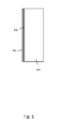
- the substrate starting material stack has been depicted in Figure 1 .
- the bottom or lower layer of the stack 1 consists of or comprises a silicon substrate (e.g. a silicon wafer) 1, the surface of which is oriented along the (100) crystal plane.
- the silicon substrate or wafer preferably comprises a notch oriented in the ⁇ 100> direction (also known to the skilled person as a 45-degree (45°) rotated notch silicon substrate), onto which a second semiconductor layer 3 is bound by means of an intermediate dielectric bonding layer 2.
- the material of the second semiconductor layer can for instance comprise or consist of Germanium, Silicon Germanium, Germanium-Tin and/or III-V materials, or any combinations of these materials.
- the intrinsic stress level within the second semiconductor layer is preferably in the range between -5 to +5 GPa.
- the second channel layer can be a strained or relaxed Ge layer.
- the intermediate dielectric bonding layer 2 can for instance be or comprise silicon oxide, silicon nitride, aluminium oxide or any combination thereof. It can be any dielectric layer 2 that allows for a mechanical bonding between the silicon bottom layer and the top material while providing electrical isolation between both layers 1 and 3.
- the specific substrate described above for a first aspect of the present invention can advantageously be used in a method for manufacturing transistor devices comprising III-V materials on a silicon substrate, according to a second aspect of the present invention.
- CMOS devices on a silicon substrate, as presented in a third aspect of the present invention.
- two different channel materials are used, both channel materials having different lattice constants than silicon and the channel materials respectively being part of transistor devices of different conductivity, for instance being respectively of the NMOS type and PMOS type, on a common silicon substrate.
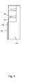
- the second semiconductor layer 3 is patterned selectively towards the intermediate dielectric bonding layer 2 or the silicon substrate layer 1 in the area where the first semiconductor channel structure and its isolation are to be provided afterwards (called n-FET region N in figure 1 ).
- active narrow silicon structures or protrusions extending from the silicon substrate, having a width smaller than 20nm are patterned and isolated in the n-FET region by using a silicon STI (Shallow Trench Isolation) process flow as it is known to the skilled person.
- silicon STI Silicon Trench Isolation
- a silicon STI process flow can for instance comprise or consists of the following steps:
- the silicon areas or protrusions 8 defined in the STI oxide have a width which is smaller than 20nm, and have a depth which is preferably larger than 40nm. This allows benefiting from an aspect ratio trapping effect during subsequent epitaxial growth of material of the channel structure in the n-FET region, as will be described below.
- temperature constraints are taken into account, such that the quality of the second semiconductor layer 3 is not compromised during the STI processing. The temperature is therefore preferably kept below 600°C.
- the method according to the second and third aspects of the present invention of the invention comprises partially removing the narrow silicon areas defined in the STI oxide to a depth larger than 40nm in the n-FET region, creating trenches 5, and refilling the trenches 5 by a semiconductor channel structure 6 (e.g. corresponding to a FIN structure of a N-FET device) by epitaxially growing a channel material (for instance a III-V material stack comprising e.g.
- a semiconductor channel structure 6 e.g. corresponding to a FIN structure of a N-FET device
- a channel material for instance a III-V material stack comprising e.g.
- the cavities can be overfilled or overgrown by growing channel material over adjacent STI isolation structures, and the epitaxially grown material which overgrew the STI isolation structures can then subsequently be removed, for instance by CMP.
- the trenches 5 can be filled by the epitaxially grown material without overgrowing the STI area.
- the material of the semiconductor channel structure 6 is preferably a crystalline material with a different lattice constant than the lattice constant of the silicon substrate 1.
- the trench depth can be about twice the trench width or can be larger than twice the trench width.
- the depth, width and orientation of the trenches is such that defects generated in the epitaxially grown layer of the material of the semiconductor structure 6 at the substrate portion at the bottom of the trench 5, which propagate in the (111) direction, are trapped by the trench sidewalls.
- the temperature is kept below 600°C during the growth of the material of the semiconductor channel structure 6, so as to not impact the quality of the second semiconductor layer 3 during this processing.
- the remaining part of the second semiconductor layer 3 is subsequently patterned to provide the appropriate channel structure, for instance FIN structure of a P-FET transistor device, in the p-FET region P as depicted in figure 1 , for the targeted device fabrication using material of the second semiconductor layer 3 as channel or active layer material.
- Gate structures 7 can then be provided on the respective semiconductor channel structures, according to processes known to the skilled person.
- the method and associated substrate of aspects of the present invention allow dual material channel integration on a silicon substrate.
- the III-V material of the semiconductor structures 6, which are preferably channel structures of transistor devices of the n-type, preferably of the FINFET type can be provided essentially defect free, by using a hetero-epitaxial growth on the silicon substrate with predetermined suitable orientation.
- Germanium based p-type transistors, preferably of the FINFET type can be integrated on the same wafer.
Landscapes
- Metal-Oxide And Bipolar Metal-Oxide Semiconductor Integrated Circuits (AREA)
- Recrystallisation Techniques (AREA)
- Element Separation (AREA)
- Thin Film Transistor (AREA)
- Insulated Gate Type Field-Effect Transistor (AREA)
Priority Applications (3)
| Application Number | Priority Date | Filing Date | Title |
|---|---|---|---|
| EP13183985.4A EP2849219A1 (de) | 2013-09-11 | 2013-09-11 | Verfahren zur Herstellung von Transistoren und zugehöriges Substrat |
| JP2014183477A JP2015056665A (ja) | 2013-09-11 | 2014-09-09 | トランジスタの製造方法および関連した基板 |
| US14/484,070 US20150076620A1 (en) | 2013-09-11 | 2014-09-11 | Method for manufacturing transistors and associated substrate |
Applications Claiming Priority (1)
| Application Number | Priority Date | Filing Date | Title |
|---|---|---|---|
| EP13183985.4A EP2849219A1 (de) | 2013-09-11 | 2013-09-11 | Verfahren zur Herstellung von Transistoren und zugehöriges Substrat |
Publications (1)
| Publication Number | Publication Date |
|---|---|
| EP2849219A1 true EP2849219A1 (de) | 2015-03-18 |
Family
ID=49123776
Family Applications (1)
| Application Number | Title | Priority Date | Filing Date |
|---|---|---|---|
| EP13183985.4A Withdrawn EP2849219A1 (de) | 2013-09-11 | 2013-09-11 | Verfahren zur Herstellung von Transistoren und zugehöriges Substrat |
Country Status (3)
| Country | Link |
|---|---|
| US (1) | US20150076620A1 (de) |
| EP (1) | EP2849219A1 (de) |
| JP (1) | JP2015056665A (de) |
Cited By (1)
| Publication number | Priority date | Publication date | Assignee | Title |
|---|---|---|---|---|
| EP3809457A1 (de) * | 2019-10-16 | 2021-04-21 | IMEC vzw | Co-integration von iii-v-bauelementen mit gruppe-iv-bauelementen |
Families Citing this family (9)
| Publication number | Priority date | Publication date | Assignee | Title |
|---|---|---|---|---|
| US9685454B2 (en) * | 2015-03-24 | 2017-06-20 | Sandisk Technologies Llc | Method of forming 3D vertical NAND with III-V channel |
| US9761604B2 (en) | 2015-03-24 | 2017-09-12 | Sandisk Technologies Llc | 3D vertical NAND with III-V channel |
| US9355914B1 (en) | 2015-06-22 | 2016-05-31 | International Business Machines Corporation | Integrated circuit having dual material CMOS integration and method to fabricate same |
| WO2016209281A1 (en) * | 2015-06-26 | 2016-12-29 | Intel Corporation | Well-based integration of heteroepitaxial n-type transistors with p-type transistors |
| US10211208B2 (en) * | 2015-06-26 | 2019-02-19 | Intel Corporation | High-mobility semiconductor source/drain spacer |
| US9437614B1 (en) | 2015-09-18 | 2016-09-06 | International Business Machines Corporation | Dual-semiconductor complementary metal-oxide-semiconductor device |
| KR102402771B1 (ko) | 2015-12-11 | 2022-05-26 | 삼성전자주식회사 | 반도체 장치 및 이의 제조 방법 |
| US10784352B2 (en) | 2015-12-26 | 2020-09-22 | Intel Corporation | Method to achieve a uniform Group IV material layer in an aspect ratio trapping trench |
| CN111613532B (zh) * | 2019-02-25 | 2023-08-22 | 中芯国际集成电路制造(上海)有限公司 | 一种场效应管的形成方法和场效应管 |
Citations (15)
| Publication number | Priority date | Publication date | Assignee | Title |
|---|---|---|---|---|
| US20040256700A1 (en) * | 2003-06-17 | 2004-12-23 | International Business Machines Corporation | High-performance CMOS devices on hybrid crystal oriented substrates |
| US20060172505A1 (en) * | 2005-01-31 | 2006-08-03 | Koester Steven J | Structure and method of integrating compound and elemental semiconductors for high-performace CMOS |
| US20060237785A1 (en) * | 2005-04-22 | 2006-10-26 | International Business Machines Corporation | Strained complementary metal oxide semiconductor (CMOS) on rotated wafers and methods thereof |
| WO2008039495A1 (en) * | 2006-09-27 | 2008-04-03 | Amberwave Systems Corporation | Tri-gate field-effect transistors formed by aspect ratio trapping |
| EP2073267A1 (de) * | 2007-12-19 | 2009-06-24 | INTERUNIVERSITAIR MICROELEKTRONICA CENTRUM vzw (IMEC) | Verfahren zur Herstellung von Halbleitervorrichtungen mit mehreren Gates und nach diesem Verfahren hergestellte Vorrichtung |
| US20100216277A1 (en) | 2008-09-19 | 2010-08-26 | Taiwan Semiconductor Manufacturing Company, Ltd. | Formation of Devices by Epitaxial Layer Overgrowth |
| US20120168823A1 (en) * | 2010-12-31 | 2012-07-05 | Zhijiong Luo | Semiconductor device and method for manufacturing the same |
| EP2521168A1 (de) * | 2011-05-03 | 2012-11-07 | Imec | Verfahren zur Herstellung einer Hybrid-MOSFET-Vorrichtung und damit hergestellte Hybrid-MOSFET-Vorrichtung |
| US20120319211A1 (en) * | 2011-06-16 | 2012-12-20 | Taiwan Semiconductor Manufacturing Company, Ltd. | Strained channel field effect transistor |
| US20130001591A1 (en) * | 2011-06-30 | 2013-01-03 | Taiwan Semiconductor Manufacturing Company, Ltd. | Finfet design and method of fabricating same |
| US20130049068A1 (en) * | 2011-08-30 | 2013-02-28 | Taiwan Semiconductor Manufacturing Company, Ltd. | Finfet device having a channel defined in a diamond-like shape semiconductor structure |
| WO2013067212A1 (en) * | 2011-11-05 | 2013-05-10 | Tokyo Electron Limited | Epitaxial film growth in retrograde wells for semiconductor devices |
| US20130134520A1 (en) * | 2011-11-25 | 2013-05-30 | Samsung Electronics Co., Ltd. | Semiconductor device and method of manufacturing the same |
| US20130168771A1 (en) * | 2011-12-30 | 2013-07-04 | Taiwan Semiconductor Manufacturing Company, Ltd. | Method of Forming CMOS FinFET Device |
| US20130175659A1 (en) * | 2012-01-05 | 2013-07-11 | Taiwan Semiconductor Manufacturing Company. Ltd. | FinFETs with Vertical Fins and Methods for Forming the Same |
Family Cites Families (1)
| Publication number | Priority date | Publication date | Assignee | Title |
|---|---|---|---|---|
| US20050136583A1 (en) * | 2003-12-23 | 2005-06-23 | Taiwan Semiconductor Manufacturing Co. | Advanced strained-channel technique to improve CMOS performance |
-
2013
- 2013-09-11 EP EP13183985.4A patent/EP2849219A1/de not_active Withdrawn
-
2014
- 2014-09-09 JP JP2014183477A patent/JP2015056665A/ja active Pending
- 2014-09-11 US US14/484,070 patent/US20150076620A1/en not_active Abandoned
Patent Citations (15)
| Publication number | Priority date | Publication date | Assignee | Title |
|---|---|---|---|---|
| US20040256700A1 (en) * | 2003-06-17 | 2004-12-23 | International Business Machines Corporation | High-performance CMOS devices on hybrid crystal oriented substrates |
| US20060172505A1 (en) * | 2005-01-31 | 2006-08-03 | Koester Steven J | Structure and method of integrating compound and elemental semiconductors for high-performace CMOS |
| US20060237785A1 (en) * | 2005-04-22 | 2006-10-26 | International Business Machines Corporation | Strained complementary metal oxide semiconductor (CMOS) on rotated wafers and methods thereof |
| WO2008039495A1 (en) * | 2006-09-27 | 2008-04-03 | Amberwave Systems Corporation | Tri-gate field-effect transistors formed by aspect ratio trapping |
| EP2073267A1 (de) * | 2007-12-19 | 2009-06-24 | INTERUNIVERSITAIR MICROELEKTRONICA CENTRUM vzw (IMEC) | Verfahren zur Herstellung von Halbleitervorrichtungen mit mehreren Gates und nach diesem Verfahren hergestellte Vorrichtung |
| US20100216277A1 (en) | 2008-09-19 | 2010-08-26 | Taiwan Semiconductor Manufacturing Company, Ltd. | Formation of Devices by Epitaxial Layer Overgrowth |
| US20120168823A1 (en) * | 2010-12-31 | 2012-07-05 | Zhijiong Luo | Semiconductor device and method for manufacturing the same |
| EP2521168A1 (de) * | 2011-05-03 | 2012-11-07 | Imec | Verfahren zur Herstellung einer Hybrid-MOSFET-Vorrichtung und damit hergestellte Hybrid-MOSFET-Vorrichtung |
| US20120319211A1 (en) * | 2011-06-16 | 2012-12-20 | Taiwan Semiconductor Manufacturing Company, Ltd. | Strained channel field effect transistor |
| US20130001591A1 (en) * | 2011-06-30 | 2013-01-03 | Taiwan Semiconductor Manufacturing Company, Ltd. | Finfet design and method of fabricating same |
| US20130049068A1 (en) * | 2011-08-30 | 2013-02-28 | Taiwan Semiconductor Manufacturing Company, Ltd. | Finfet device having a channel defined in a diamond-like shape semiconductor structure |
| WO2013067212A1 (en) * | 2011-11-05 | 2013-05-10 | Tokyo Electron Limited | Epitaxial film growth in retrograde wells for semiconductor devices |
| US20130134520A1 (en) * | 2011-11-25 | 2013-05-30 | Samsung Electronics Co., Ltd. | Semiconductor device and method of manufacturing the same |
| US20130168771A1 (en) * | 2011-12-30 | 2013-07-04 | Taiwan Semiconductor Manufacturing Company, Ltd. | Method of Forming CMOS FinFET Device |
| US20130175659A1 (en) * | 2012-01-05 | 2013-07-11 | Taiwan Semiconductor Manufacturing Company. Ltd. | FinFETs with Vertical Fins and Methods for Forming the Same |
Cited By (2)
| Publication number | Priority date | Publication date | Assignee | Title |
|---|---|---|---|---|
| EP3809457A1 (de) * | 2019-10-16 | 2021-04-21 | IMEC vzw | Co-integration von iii-v-bauelementen mit gruppe-iv-bauelementen |
| US11557503B2 (en) | 2019-10-16 | 2023-01-17 | Imec Vzw | Method for co-integration of III-V devices with group IV devices |
Also Published As
| Publication number | Publication date |
|---|---|
| JP2015056665A (ja) | 2015-03-23 |
| US20150076620A1 (en) | 2015-03-19 |
Similar Documents
| Publication | Publication Date | Title |
|---|---|---|
| EP2849219A1 (de) | Verfahren zur Herstellung von Transistoren und zugehöriges Substrat | |
| US9741800B2 (en) | III-V multi-channel FinFETs | |
| KR101622048B1 (ko) | 누설이 감소된 cmos 디바이스 및 그 형성 방법 | |
| US9882026B2 (en) | Method for forming a nanowire structure | |
| US9917179B2 (en) | Stacked nanowire devices formed using lateral aspect ratio trapping | |
| JP6786755B2 (ja) | 異なる歪み状態を有するフィン構造を含む半導体構造を作製するための方法及び関連する半導体構造 | |
| KR101410072B1 (ko) | 트렌치들에서 반도체 영역들을 형성하는 방법 | |
| US9330908B2 (en) | Semiconductor structure with aspect ratio trapping capabilities | |
| US9859425B2 (en) | Field-effect transistor with aggressively strained fins | |
| CN102593037B (zh) | 半导体结构及其制作方法 | |
| US9123627B1 (en) | Methods of forming alternative material fins with reduced defect density for a FinFET semiconductor device | |
| US9368604B1 (en) | Method of removing threading dislocation defect from a fin feature of III-V group semiconductor material | |
| CN105870061B (zh) | 用于绝缘体上应变硅晶片上双重隔离的方法和装置 | |
| KR20170132074A (ko) | 희생 에피택셜 게이트 스트레서 | |
| TWI642106B (zh) | 絕緣體上半導體元件的製造方法 | |
| EP2897161A1 (de) | Verfahren zur Herstellung einer CMOS-Vorrichtung | |
| CN107004712B (zh) | 利用基于深宽比沟槽的工艺形成均匀层 | |
| US20170117414A1 (en) | Semiconductor structure and manufacturing method thereof | |
| KR102203033B1 (ko) | 평면형 이종 디바이스 | |
| EP3300117B1 (de) | Verfahren zur herstellung eines halbleiterbauelements mit kanal mit hohem aspektverhältnis | |
| CN102790006B (zh) | 半导体结构及其制作方法 | |
| EP3093881B1 (de) | Verfahren zur herstellung einer cmos-vorrichtung | |
| CN103855005B (zh) | 双应力异质soi半导体结构及其制造方法 | |
| EP2779212A2 (de) | Verfahren zur Herstellung eines Halbleiterbauelements mit hoher Elektronenbeweglichkeit |
Legal Events
| Date | Code | Title | Description |
|---|---|---|---|
| PUAI | Public reference made under article 153(3) epc to a published international application that has entered the european phase |
Free format text: ORIGINAL CODE: 0009012 |
|
| 17P | Request for examination filed |
Effective date: 20130911 |
|
| AK | Designated contracting states |
Kind code of ref document: A1 Designated state(s): AL AT BE BG CH CY CZ DE DK EE ES FI FR GB GR HR HU IE IS IT LI LT LU LV MC MK MT NL NO PL PT RO RS SE SI SK SM TR |
|
| AX | Request for extension of the european patent |
Extension state: BA ME |
|
| R17P | Request for examination filed (corrected) |
Effective date: 20150909 |
|
| RBV | Designated contracting states (corrected) |
Designated state(s): AL AT BE BG CH CY CZ DE DK EE ES FI FR GB GR HR HU IE IS IT LI LT LU LV MC MK MT NL NO PL PT RO RS SE SI SK SM TR |
|
| 17Q | First examination report despatched |
Effective date: 20161125 |
|
| STAA | Information on the status of an ep patent application or granted ep patent |
Free format text: STATUS: THE APPLICATION IS DEEMED TO BE WITHDRAWN |
|
| 18D | Application deemed to be withdrawn |
Effective date: 20170607 |