EP2270887B1 - Blocs de photoemetteurs haute puissance a optiques compactes - Google Patents
Blocs de photoemetteurs haute puissance a optiques compactes Download PDFInfo
- Publication number
- EP2270887B1 EP2270887B1 EP10185708.4A EP10185708A EP2270887B1 EP 2270887 B1 EP2270887 B1 EP 2270887B1 EP 10185708 A EP10185708 A EP 10185708A EP 2270887 B1 EP2270887 B1 EP 2270887B1
- Authority
- EP
- European Patent Office
- Prior art keywords
- encapsulant
- light
- light emitter
- light source
- supporting surface
- Prior art date
- Legal status (The legal status is an assumption and is not a legal conclusion. Google has not performed a legal analysis and makes no representation as to the accuracy of the status listed.)
- Active
Links
Images

Classifications
-
- H—ELECTRICITY
- H01—ELECTRIC ELEMENTS
- H01L—SEMICONDUCTOR DEVICES NOT COVERED BY CLASS H10
- H01L33/00—Semiconductor devices with at least one potential-jump barrier or surface barrier specially adapted for light emission; Processes or apparatus specially adapted for the manufacture or treatment thereof or of parts thereof; Details thereof
- H01L33/48—Semiconductor devices with at least one potential-jump barrier or surface barrier specially adapted for light emission; Processes or apparatus specially adapted for the manufacture or treatment thereof or of parts thereof; Details thereof characterised by the semiconductor body packages
- H01L33/52—Encapsulations
- H01L33/54—Encapsulations having a particular shape
-
- H—ELECTRICITY
- H01—ELECTRIC ELEMENTS
- H01L—SEMICONDUCTOR DEVICES NOT COVERED BY CLASS H10
- H01L33/00—Semiconductor devices with at least one potential-jump barrier or surface barrier specially adapted for light emission; Processes or apparatus specially adapted for the manufacture or treatment thereof or of parts thereof; Details thereof
- H01L33/48—Semiconductor devices with at least one potential-jump barrier or surface barrier specially adapted for light emission; Processes or apparatus specially adapted for the manufacture or treatment thereof or of parts thereof; Details thereof characterised by the semiconductor body packages
- H01L33/58—Optical field-shaping elements
- H01L33/60—Reflective elements
-
- H—ELECTRICITY
- H01—ELECTRIC ELEMENTS
- H01L—SEMICONDUCTOR DEVICES NOT COVERED BY CLASS H10
- H01L33/00—Semiconductor devices with at least one potential-jump barrier or surface barrier specially adapted for light emission; Processes or apparatus specially adapted for the manufacture or treatment thereof or of parts thereof; Details thereof
- H01L33/48—Semiconductor devices with at least one potential-jump barrier or surface barrier specially adapted for light emission; Processes or apparatus specially adapted for the manufacture or treatment thereof or of parts thereof; Details thereof characterised by the semiconductor body packages
- H01L33/64—Heat extraction or cooling elements
- H01L33/641—Heat extraction or cooling elements characterized by the materials
-
- H—ELECTRICITY
- H01—ELECTRIC ELEMENTS
- H01L—SEMICONDUCTOR DEVICES NOT COVERED BY CLASS H10
- H01L2224/00—Indexing scheme for arrangements for connecting or disconnecting semiconductor or solid-state bodies and methods related thereto as covered by H01L24/00
- H01L2224/01—Means for bonding being attached to, or being formed on, the surface to be connected, e.g. chip-to-package, die-attach, "first-level" interconnects; Manufacturing methods related thereto
- H01L2224/42—Wire connectors; Manufacturing methods related thereto
- H01L2224/47—Structure, shape, material or disposition of the wire connectors after the connecting process
- H01L2224/48—Structure, shape, material or disposition of the wire connectors after the connecting process of an individual wire connector
- H01L2224/4805—Shape
- H01L2224/4809—Loop shape
- H01L2224/48091—Arched
-
- H—ELECTRICITY
- H01—ELECTRIC ELEMENTS
- H01L—SEMICONDUCTOR DEVICES NOT COVERED BY CLASS H10
- H01L2924/00—Indexing scheme for arrangements or methods for connecting or disconnecting semiconductor or solid-state bodies as covered by H01L24/00
- H01L2924/10—Details of semiconductor or other solid state devices to be connected
- H01L2924/11—Device type
- H01L2924/12—Passive devices, e.g. 2 terminal devices
- H01L2924/1204—Optical Diode
- H01L2924/12044—OLED
-
- H—ELECTRICITY
- H01—ELECTRIC ELEMENTS
- H01L—SEMICONDUCTOR DEVICES NOT COVERED BY CLASS H10
- H01L33/00—Semiconductor devices with at least one potential-jump barrier or surface barrier specially adapted for light emission; Processes or apparatus specially adapted for the manufacture or treatment thereof or of parts thereof; Details thereof
- H01L33/48—Semiconductor devices with at least one potential-jump barrier or surface barrier specially adapted for light emission; Processes or apparatus specially adapted for the manufacture or treatment thereof or of parts thereof; Details thereof characterised by the semiconductor body packages
- H01L33/52—Encapsulations
- H01L33/56—Materials, e.g. epoxy or silicone resin
-
- H—ELECTRICITY
- H01—ELECTRIC ELEMENTS
- H01L—SEMICONDUCTOR DEVICES NOT COVERED BY CLASS H10
- H01L33/00—Semiconductor devices with at least one potential-jump barrier or surface barrier specially adapted for light emission; Processes or apparatus specially adapted for the manufacture or treatment thereof or of parts thereof; Details thereof
- H01L33/48—Semiconductor devices with at least one potential-jump barrier or surface barrier specially adapted for light emission; Processes or apparatus specially adapted for the manufacture or treatment thereof or of parts thereof; Details thereof characterised by the semiconductor body packages
- H01L33/58—Optical field-shaping elements
Definitions
- This invention relates to light emitters and, more particularly, to light emitter packages with components arranged to withstand thermal stresses.
- Light emitters are an important class of solid-state devices that convert electrical energy to light.
- One such light emitter is a light emitting diode (LED) which generally includes an active region of semi-conductive material sandwiched between two oppositely doped regions. When a bias is applied across the doped regions, holes and electrons are injected into the active region where they recombine to generate light. The light can be emitted from the active region and through the surfaces of the LED.
- LED light emitting diode
- LEDs are generally divided into classes depending on their power rating. Although there is no standard range for the different classes, low power LEDs typically have a power rating in the range of 0.1 Watts to 0.3 Watts, or lower, and high power LEDs typically have a rating in the range of 0.5 Watts to 1.0 Watt, or higher.
- Conventional packaging for low power LEDs typically includes a reflector cup with the LED mounted at the bottom of the cup. Cathode and anode leads are electrically coupled to the LED to provide power.
- the cathode lead can extend through the reflector cup and the anode lead can be wire bonded.
- the main function of the reflector cup is to redirect light emitted in certain directions in order to control the far-field intensity pattern of the LED.
- the reflector cup can include a highly reflective surface finish and can be plate stamped or metal plated with a metal such as aluminum (Al) or silver (Ag).
- the entire structure can be encased in a transparent, hard encapsulant such as a plastic or epoxy.
- the encapsulant serves a number of functions. One function is to provide a hermetic seal for the LED chip. In another function, light refracts at the encapsulant/air interface, so that the outside shape of the encapsulant can act as a lens to further control the intensity pattern of the LED.
- the LED chip, the reflector cup, and the encapsulant each generally have different coefficients of thermal expansion (CTE).
- CTE coefficients of thermal expansion
- epoxies and silicones typically used for the encapsulant have a CTE that is very different from the CTE of metals or ceramics.
- the CTE mismatch can also be exacerbated by constraints imposed by the manufacturing flow, such as during epoxy curing.
- these packages do not dissipate heat from the LED chip efficiently as they lack good thermal properties. However, because the LED operates at low power, the amount of heat it produces is relatively low so that the differences in CTE do not result in unacceptable failure rates.
- High power LEDs are generally larger, use larger packaging components, and generate higher amounts of heat.
- the CTE mismatch has a much larger impact on reliability and if the low-power LED type packaging is used, the differences in CTE for the packaging components can result in unacceptable failure rates.
- One of the most common failures is fracturing or cracking of the encapsulant.
- High power LED packages have been introduced having a heat spreader that serves as a rigid platform for the remainder of the components, and is made of a material with high thermal conductivity such as a metal or ceramic that helps to radiate heat away from the LED chip.
- a reflector cup is mounted to the platform with the LED chip mounted at the bottom of the cup.
- the LED chip is contacted by wire bonds from the rigid platform.
- the reflector cup, LED chip and wire bonds are encased in an optically clear material that provides environmental protection.
- the optically clear material can include a soft gel such as silicone. As the different components expand and contract through thermal cycles, the soft gel readily deforms and compensates for the different CTEs.
- soft gel is not as robust as plastics, epoxies, and glass, and cannot be used in some harsh environments without a coating or cover to act as a hermetic seal, which adds complexity to the LED fabrication process.
- the soft gel also tends to absorb water, which can shorten the LED's lifespan. It is also more difficult to shape soft gels to control the emission pattern of the LED package.
- U.S. Patent No. 6,274,924 to Carey et al. discloses another high power LED package that includes a heat sinking slug that is inserted into an insert molded leadframe.
- the slug can include a reflector cup with the LED chip and thermally conductive submount arranged at the base of the cup.
- Metal leads are electrically and thermally isolated from the slug.
- An optical lens is added by mounting a thermoplastic lens over the slug.
- the lens can be molded to leave room for a soft encapsulant between the LED and the inside surface of the lens.
- This invention claims to operate reliably under high power conditions, but is complex, difficult to manufacture, and expensive.
- the thermoplastic lens also does not survive high temperatures typically used for the process of soldering LEDs to a printed circuit board.
- the present invention seeks to provide LED packages that are particularly adapted to use with high power LEDs and are arranged to reduce the LED package failures due to the differences in the CTE for the package components.
- the LED packages are also simple, flexible, and rugged.
- a light emitter is defined in claim 1. This comprises a substantially supporting surface, a light source positioned on the supporting surface, and an encapsulant positioned on the supporting surface.
- the encapsulant may surround the light source and be capable of expanding and contracting in response to a change in temperature, constrained only by adhesion to said planar support surface.
- a light emitter comprises a heat spreader and a light source positioned in thermal contact with a substantially planar surface of the heat spreader.
- the heat spreader provides support for said light source and an encapsulant is positioned to surround the light source, with the encapsulant capable of expanding and/or contracting in response to a change in temperature constrained only by adhesion to said planar surface.
- a first reflective element is positioned to reflect light from the light source, the reflective element being integrated with at least one of the heat spreader and the encapsulant.
- an optical display comprises a heat spreader with a substantially planar surface.
- a plurality of light emitters are positioned on the planar surface with each light emitter comprising a light source positioned in thermal contact with the heat spreader.
- An encapsulant is positioned on the heat spreader to surround the light source with the encapsulant being capable of expanding and contracting in response to a change in temperature constrained only by adhesion to said planar surface.
- Each light emitter comprises at least one reflective element positioned on the heat spreader and/or said encapsulants to increase the light emitting efficiency of the display.
- One example of a method of fabricating a light emitter includes providing a substantially planar supporting surface and providing a light source positioned on the substantially planar supporting surface. An encapsulant is provided positioned on the supporting surface and over the light source so that the encapsulant can expand and contract with changes in temperature constrained only by adhesion to said planar surface.
- FIG. 1 illustrates one example of a light emitter 10.
- Emitter 10 includes a heat spreader 12 with a light source 14 is positioned on and in thermal contact with the heat spreader region 12.
- Spreader region 12 provides a support structure for holding light source 14 and is at least partially made of a high thermal conductivity material to facilitate heat flow away from light source 14.
- the preferred heat spreader is made of a high thermal conductive material such as copper (Cu), aluminum (Al), aluminum nitride (AlN), aluminum oxide (AlO), silicon (Si), silicon carbide (SiC) or combinations thereof.
- Light source 14 comprises an LED, although it can include other light emitters, such as a solid-state laser, a laser diode, or an organic light emitting diode, among others.
- Power to light source 14 can be provided from first and second wire bonds 16, 18 with a bias applied across the light source 14, and in the embodiment shown the wire bonds apply a bias across oppositely doped layers of the LED light source to cause it to emit light.
- first and second wire bonds 16, 18 with a bias applied across the light source 14
- the wire bonds apply a bias across oppositely doped layers of the LED light source to cause it to emit light.
- only one wire bond can be used, with the light source 14 also contacted through the spreader region 12.
- the light source 14 is contacted only through the spreader region 12.
- Emitters according to the present invention can be included in systems designed to emit light either as a single light source or in a display.
- Emitter according to the invention can also include a single light source or an array of light sources which emit the same or different wavelengths of light.
- Emitter 10 and the emitters in the following figures are shown with one light source for simplicity and ease of discussion. It is understood, however, that emitters according to the present invention can be arranged in many different ways.
- a transparent encapsulant 20 is positioned to surround light source 14 and is provided to encapsulate and hermetically seal light source 14 and wire bonds 16, 18.
- Encapsulant 20 is typically positioned on the top surface of spreader region 20.
- Encapsulant 20 can be made of many different hard and optically clear materials such as epoxy, silicone, glass, or plastic, and can be a pre-molded lens or formed directly over light source 14. Pre-molded encapsulants or lenses can be fabricated using techniques, such as injection molding, and then bonded to heat spreader 20.
- the spreader region 12 can also include a reflective layer 22 on the same surface as the light source 14, with the reflective layer 22 at least covering substantially all of the surface not covered by the light source 14.
- the reflective layer 22 covers the entire surface such that part of said reflective layer is sandwiched between the light source 14 and the spreader region 12.
- Light source 14 emits light omnidirectionally with light paths 1, 2, 3, 4 and 5 representing a few of the possible light paths from the light source.
- Light paths 1, 2 and 3 extend from light source 14 and through encapsulant 20.
- Light can also flow along light paths 4 and 5 which extend from light source 14 to the reflective layer 22 and through encapsulant 20.
- Reflective layer 22 can reflect light from light source 14 to increase the optical efficiency of emitter 10.
- Reflective layer 22 can comprise many reflective materials reflective at the wavelength of interest, such as aluminum (Al), silver (Ag), or a combination thereof.
- Emitter 10 has many advantages, one being that it is less complex and, consequently, costs less than conventional devices.
- the complexity is reduced in one way by combining the reflector layer 22 with spreader region 12 which eliminates the need to have a reflector structure separate from encapsulant 20 and heat spreader 12, which allows for a simplified manufacturing process.
- Thermal stresses are also reduced because the reflector function is integrated with other components included in emitter 10. Hence, there are fewer components expanding and contracting against each other at different rates. As a result, light source 14 can operate more reliably at higher power and, consequently, higher temperature with less risk of having emitter 10 fail.
- Another cause of failure can be the fracturing or cracking of encapsulant 20 associated with CTE mismatch between the different materials used. However, the probability of this happening is reduced by the arrangement of emitter 10.
- the surface between encapsulant 20 and spreader region 12 is planar so that encapsulant 20 is only constrained at one surface. This puts less stress on wire bonds 16 and/or 18 which can cause them to break or loosen and reduce the useful lifetime of emitter 10.
- Encapsulant 20 can include hard and high melting point materials, such as glass, to provide a package which is hermetically sealed because the curing process and temperature cycles associated with these materials is no longer a problem.
- Emitter 10 also provides for greater flexibility in the choice of materials which can be used for encapsulant 20 and spreader region 22 because they can be matched for adhesion. Hence, the probability of encapsulant 20 delaminating and peeling away from spreader layer 22 through the emitter's thermal cycles is reduced.
- light emitter 10 has a smaller footprint so that an array of packages can be positioned closer together. This feature is useful in light displays where it is typically desired to position the packages close together in an array to increase resolution and display quality.
- FIGS. 2 through 8 illustrate additional embodiments of light emitters. It should be noted that the emitters illustrated in the rest of the disclosure include components similar to the components illustrated in FIG. 1 and similar numbering is used with the understanding that the discussion above in conjunction with emitter 10 applies equally well to the emitters discussed in FIGS. 2 through 8 .
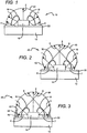
- FIG. 2 illustrates an embodiment of a light emitter 30 in accordance with the present invention.
- Emitter 30 includes spreader region 12 and can include a reflective layer 22.
- Light source 14 is positioned on reflective layer 22 and an encapsulant 40 is positioned to encapsulate and seal light source 14.
- Encapsulant 40 is shaped around its base to provide an angled surface 42 that reflects sideways directed light emitted from light source 14 by total internal reflection.
- Light paths 6, 7 show two possible light paths from the light source 14, both of which are incident to surface 42.
- Light paths 6 and 7 can be reflected by total internal reflection (TIR) by surface 42 toward the top of encapsulant 40 along respective light paths 8 and 9. This reduces the light that is emitted out the sides of encapsulant 40 and increases the light emitted out of the top.
- emitter 30 can produce more focused light with better light emission efficiency.
- light emitted from light source 14 can also be reflected from reflective layer 22 and through encapsulant 40, either directly or indirectly off of surface 42 to further enhance emission efficiency.
- Light emitter 30 includes all of the features of emitter 10 described above, with the added advantage of more focused light, better optical efficiency.
- FIG. 3 illustrates another embodiment of a light emitter 50 in accordance with the present invention, which is similar to emitter 30 in FIG. 2 .
- Emitter 50 includes spreader region 12 with a reflective layer 22 on the spreader region 12.
- a light source 14 is positioned on reflective layer 22 and an encapsulant 60 positioned to surround light source 14 and to provide hermetic sealing.
- Encapsulant 60 also comprises an angled surface 42 with reflective layer 64 applied to angled surface 42.
- Support region 49 is positioned adjacent to second reflective layer 64 and spreader region 22.
- Second reflective layer 64 reflects most or all of the light incident on the angled surface 42 including the light that does not experience TIR and would otherwise pass through angled surface 42. This further focuses the light from light source 14 toward the top of encapsulant 60 and increases the optical efficiency by increasing the amount of emitted light.
- Second reflective layer 64 can be made of different materials with different reflectivities, such as silver (Ag), aluminum (Al), titanium oxide (TiO), white resin, or combinations thereof. Second reflective layer 64 can be applied using many different methods such as painting, plating, or deposition and can also be applied before or after encapsulant 60 is positioned over light source 14.
- layer 64 which is opaque to light, is that it allows optional barrier region 49 to be included for mechanical support and environmental protection without degrading the light efficiency of emitter 50.
- the material used for region 49 should be chosen so that it does not constrain the encapsulant 60 under thermal cycling.
- FIG. 4 illustrates another embodiment of light emitter 70, which is similar to emitter 10 of FIG. 1 .
- Emitter 70 includes spreader region 12, light source 14, and a reflective layer 22.
- Emitter 70 also comprises an encapsulant 80 that is a preformed lens having a cavity 81 in its base.
- lens 80 can be made of an epoxy, silicone, glass, or plastic and can be fabricated using methods such as injection molding.
- Encapsulant 80 is mounted over light source 14 to the top surface of heat spreader 12 with light source 14 and wire bonds 16, 18 arranged in cavity 81.
- a bonding material 82 fills the space in cavity 81 and holds lens 80 to heat spreader 12.
- Different types of encapsulants can be used provided they are sized to fit on heat spreader 12 while providing a cavity for light source 14, wire bonds 16, 18 and bonding material 82.
- Bonding material 82 can include different materials such as an epoxy, glue, or silicone gel.
- the index of refraction of bonding material 82 is preferably the same as that of encapsulant 80 to minimize reflections between the two materials and can be chosen to obtain a desired light emitting efficiency.
- Material 82 can be positioned in cavity 81 before encapsulant 80 is positioned over light source 14 or encapsulant 80 can be positioned in place and material 82 can be injected through encapsulant 80 or through a hole (not shown) in heat spreader 12. The hole can then be sealed with a plug made from resin or a similar material.
- This arrangement has the advantages of emitter 10 with added flexibility in the type and shape of encapsulant that can be mounted over light source 14 and heat spreader 12. Different types of lenses can be used provided they are sized on the spreader region 12 while providing a cavity for the light emitter 14, wire bonds 16, 18, and the bonding material 82. If silicone gel is used for material 82, then it can compensate for differences in the CTE of the different materials.
- FIG. 5 illustrates another embodiment of a light emitter 90.
- Emitter 90 includes spreader region 12, light source 14, and reflective layer 22.
- Emitter 90 also includes a hard "bullet shaped" encapsulant 100, which can be a pre-molded lens or an epoxy positioned over light source 14 and shaped.
- the shape of encapsulant 100 is chosen to refract light along light paths 1, 3, 4, and 5 toward the top of emitter 90 as the light passes out of encapsulant 100 at a surface 121. This light refraction helps to focus the light from light source 14. Light that hits the surface of encapsulant 100 at exactly 90° (i.e. along light path 2) will not be refracted.
- FIG. 6 illustrates another embodiment of a light emitter 110 according to the present invention which also includes a spreader region 12, light source 14, and reflective layer 22.
- Emitter 110 also includes a "concave" shaped encapsulant 120 that more effectively reflects light internally toward the top of emitter 110 and can also more efficiently refract light passing out of the encapsulant 120 toward the top of the emitter 110.
- Encapsulant 120 includes an angled surface 122 which is shaped in such a way to increase the focusing power of encapsulant 120 and the light emitting efficiency of emitter 110. The angle and shape of surface 122 can be chosen to obtain a desired gain in focusing the light and to decrease any losses from TIR.
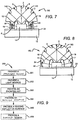
- FIG. 7 illustrates another embodiment of light emitter 130 in accordance with the present invention that comprises spreader region 12, light source 14, wire bonds 16 and 18, and reflective layer 22.
- Emitter 130 also comprises a mushroom shaped encapsulant 140 having a dome 142 and angled stem 146.
- Stem 146 can be covered by a second reflective layer 147 such that light from light source 14 that strikes stem 146 along light paths 6 and 7 is reflected toward dome 142 along respective light paths 8 and 9.
- This arrangement also provides focused light and is more efficient because less light is lost to TIR.
- FIG. 8 illustrates still another embodiment of a light emitter 150 in accordance with the present invention, which includes a spreader region 12, light source 14, and reflective layer 22.
- Emitter 150 also includes a spherical shape encapsulant 160 that can also include a reflective region 161 on its lower hemisphere to reflect light along light paths 6 and 7 toward the top of encapsulant 160 along respective light paths 8 and 9.
- This arrangement also provides focused light and has less TIR losses because of encapsulant 160 and reflective region 64.
- the encapsulant can be many other detailed shapes in accordance with the present invention.
- FIG. 9 illustrates a flowchart 200 for one embodiment of a method for fabricating a light emitter in accordance with the present invention.
- the method includes step 201 of providing a spreader region having at least one planar surface with a reflective layer on it, and step 202 includes providing a light source positioned on at least one planar surface.
- Step 203 comprises providing an encapsulant positioned on the planar surface of the spreader region and over the light source.
- the encapsulant can be positioned so that it hermetically seals the light source, where the hermetic seal remains unbroken with changes in temperature.
- the encapsulant can be positioned so that the relative position of the encapsulant and light source remains unchanged with changes in temperature. The relative position will remain unchanged if there is nothing (i.e. a 3D reflector structure) for the encapsulant to push against as the temperature changes.
- An optional step 204 comprises angling the surface of the encapsulant adjacent to the spreader region to increase the efficiency of the emitter by directing TIR light and refracted light toward the top of the emitter.
- An optional step 205 comprises providing a second reflective element positioned on the angled surfaces to increase the emission efficiency of the emitter.
- the second reflective element can be formed by using one of painting, plating, and deposition.
- An optional step 207 can comprise positioning a barrier region adjacent to the supporting surface and a base of the encapsulant. The barrier region can form a better seal for the light source. It should be noted that the steps illustrated in flowchart 200 can be performed in a different order and that different steps can be used in methods according to the present invention.
- each of the light sources described above can further comprise a submount to provide protection from electrostatic discharge (ESD).
- ESD electrostatic discharge
- the heat spreader can be etched to provide a hole to house the light source such that the light source does not extend above the top surface of the heat spreader.
- the encapsulant could then have a flat base to mount to the heat spreader, over the light source.
Claims (14)
- Émetteur de lumière (30, 50, 70, 90, 110, 150), comprenant :une source de lumière à semi-conducteur (14) positionnée sur une surface de support essentiellement plane ; etun élément d'encapsulation (40, 60, 80, 100, 120, 140, 160) positionné sur ladite surface de support essentiellement plane au-dessus de ladite source de lumière, ledit élément d'encapsulation comprenant une forme concave, convexe, de champignon, sphérique ou de dôme au-dessus de ladite source de lumière, où ledit élément d'encapsulation est plus étroit au niveau de ladite surface de support essentiellement plane qu'en un point situé au-dessus de ladite surface de support,caractérisé en ce que ledit élément d'encapsulation est contraint par ladite surface de support essentiellement plane uniquement.
- Émetteur de lumière de la revendication 1, dans lequel ladite surface de support essentiellement plane comprend un dissipateur de chaleur hautement thermoconducteur (12).
- Émetteur de lumière de la revendication 1, comprenant en outre un élément réfléchissant (22) intégré à au moins l'un(e) de ladite surface de support et dudit élément d'encapsulation.
- Émetteur de lumière de la revendication 1, dans lequel ladite surface de support comprend du nitrure d'aluminium.
- Émetteur de lumière de la revendication 1, dans lequel ladite surface de support comprend un métal.
- Émetteur de lumière de la revendication 1, dans lequel ledit élément d'encapsulation est formé au-dessus dudit émetteur de lumière.
- Émetteur de lumière de la revendication 1, dans lequel ledit élément d'encapsulation est prémoulé.
- Émetteur de lumière de la revendication 1, dans lequel ledit élément d'encapsulation forme un dôme au-dessus de ladite source de lumière.
- Émetteur de lumière de la revendication 1, dans lequel ledit élément d'encapsulation scelle hermétiquement ladite source de lumière.
- Émetteur de lumière de la revendication 1, dans lequel ledit élément d'encapsulation comprend une lentille dimensionnée sur ladite surface de support.
- Émetteur de lumière de la revendication 1, dans lequel ledit élément d'encapsulation est capable de se dilater et de se contracter et dans lequel ladite dilatation et ladite contraction sont limitées uniquement par ladite surface de support essentiellement plane.
- Émetteur de lumière de la revendication 11, dans lequel ledit élément d'encapsulation est capable de se dilater et de se contracter en réponse à un changement de température.
- Émetteur de lumière de la revendication 12, dans lequel ladite dilatation et ladite contraction sont limitées uniquement par ladite surface de support essentiellement plane de sorte qu'une position relative dudit élément d'encapsulation et de ladite source de lumière reste inchangée avec ledit changement de température.
- Émetteur de lumière de l'une quelconque des revendications 11 à 13, dans lequel ladite dilatation et ladite contraction sont limitées uniquement par adhérence sur ladite surface de support essentiellement plane.
Applications Claiming Priority (3)
| Application Number | Priority Date | Filing Date | Title |
|---|---|---|---|
| US46719303P | 2003-04-30 | 2003-04-30 | |
| PCT/US2004/013256 WO2004100279A2 (fr) | 2003-04-30 | 2004-04-28 | Blocs de photoemetteurs haute puissance a optiques compactes |
| EP04750926.0A EP1620903B1 (fr) | 2003-04-30 | 2004-04-28 | Blocs de photoemetteurs haute puissance a optiques compactes |
Related Parent Applications (3)
| Application Number | Title | Priority Date | Filing Date |
|---|---|---|---|
| EP04750926.0A Division EP1620903B1 (fr) | 2003-04-30 | 2004-04-28 | Blocs de photoemetteurs haute puissance a optiques compactes |
| EP04750926.0A Division-Into EP1620903B1 (fr) | 2003-04-30 | 2004-04-28 | Blocs de photoemetteurs haute puissance a optiques compactes |
| EP04750926.0 Division | 2004-04-28 |
Publications (2)
| Publication Number | Publication Date |
|---|---|
| EP2270887A1 EP2270887A1 (fr) | 2011-01-05 |
| EP2270887B1 true EP2270887B1 (fr) | 2020-01-22 |
Family
ID=33435034
Family Applications (3)
| Application Number | Title | Priority Date | Filing Date |
|---|---|---|---|
| EP10185708.4A Active EP2270887B1 (fr) | 2003-04-30 | 2004-04-28 | Blocs de photoemetteurs haute puissance a optiques compactes |
| EP04750926.0A Active EP1620903B1 (fr) | 2003-04-30 | 2004-04-28 | Blocs de photoemetteurs haute puissance a optiques compactes |
| EP10185698.7A Active EP2264798B1 (fr) | 2003-04-30 | 2004-04-28 | Blocs de photoemetteurs haute puissance a optiques compactes |
Family Applications After (2)
| Application Number | Title | Priority Date | Filing Date |
|---|---|---|---|
| EP04750926.0A Active EP1620903B1 (fr) | 2003-04-30 | 2004-04-28 | Blocs de photoemetteurs haute puissance a optiques compactes |
| EP10185698.7A Active EP2264798B1 (fr) | 2003-04-30 | 2004-04-28 | Blocs de photoemetteurs haute puissance a optiques compactes |
Country Status (8)
| Country | Link |
|---|---|
| US (1) | US9666772B2 (fr) |
| EP (3) | EP2270887B1 (fr) |
| JP (2) | JP2006525682A (fr) |
| KR (1) | KR101148332B1 (fr) |
| CN (2) | CN101556985B (fr) |
| CA (1) | CA2523544A1 (fr) |
| TW (2) | TWI484665B (fr) |
| WO (1) | WO2004100279A2 (fr) |
Families Citing this family (165)
| Publication number | Priority date | Publication date | Assignee | Title |
|---|---|---|---|---|
| DE60330023D1 (de) | 2002-08-30 | 2009-12-24 | Lumination Llc | Geschichtete led mit verbessertem wirkungsgrad |
| US10340424B2 (en) | 2002-08-30 | 2019-07-02 | GE Lighting Solutions, LLC | Light emitting diode component |
| US7800121B2 (en) | 2002-08-30 | 2010-09-21 | Lumination Llc | Light emitting diode component |
| US7224000B2 (en) * | 2002-08-30 | 2007-05-29 | Lumination, Llc | Light emitting diode component |
| CA2523544A1 (fr) | 2003-04-30 | 2004-11-18 | Cree, Inc. | Blocs de photoemetteurs haute puissance a optiques compactes |
| US7005679B2 (en) | 2003-05-01 | 2006-02-28 | Cree, Inc. | Multiple component solid state white light |
| US7777235B2 (en) * | 2003-05-05 | 2010-08-17 | Lighting Science Group Corporation | Light emitting diodes with improved light collimation |
| US6803607B1 (en) * | 2003-06-13 | 2004-10-12 | Cotco Holdings Limited | Surface mountable light emitting device |
| US6995402B2 (en) * | 2003-10-03 | 2006-02-07 | Lumileds Lighting, U.S., Llc | Integrated reflector cup for a light emitting device mount |
| JP3987485B2 (ja) * | 2003-12-25 | 2007-10-10 | セイコーエプソン株式会社 | 光源装置及びプロジェクタ |
| US7355284B2 (en) | 2004-03-29 | 2008-04-08 | Cree, Inc. | Semiconductor light emitting devices including flexible film having therein an optical element |
| KR100623024B1 (ko) * | 2004-06-10 | 2006-09-19 | 엘지전자 주식회사 | 고출력 led 패키지 |
| WO2006059828A1 (fr) * | 2004-09-10 | 2006-06-08 | Seoul Semiconductor Co., Ltd. | Boitier pour diode electroluminescente contenant plusieurs resines de moulage |
| US7748873B2 (en) * | 2004-10-07 | 2010-07-06 | Seoul Semiconductor Co., Ltd. | Side illumination lens and luminescent device using the same |
| US7344902B2 (en) * | 2004-11-15 | 2008-03-18 | Philips Lumileds Lighting Company, Llc | Overmolded lens over LED die |
| US7858408B2 (en) * | 2004-11-15 | 2010-12-28 | Koninklijke Philips Electronics N.V. | LED with phosphor tile and overmolded phosphor in lens |
| US7452737B2 (en) * | 2004-11-15 | 2008-11-18 | Philips Lumileds Lighting Company, Llc | Molded lens over LED die |
| US7352011B2 (en) * | 2004-11-15 | 2008-04-01 | Philips Lumileds Lighting Company, Llc | Wide emitting lens for LED useful for backlighting |
| KR100580753B1 (ko) * | 2004-12-17 | 2006-05-15 | 엘지이노텍 주식회사 | 발광소자 패키지 |
| US9070850B2 (en) | 2007-10-31 | 2015-06-30 | Cree, Inc. | Light emitting diode package and method for fabricating same |
| US7821023B2 (en) | 2005-01-10 | 2010-10-26 | Cree, Inc. | Solid state lighting component |
| US9793247B2 (en) | 2005-01-10 | 2017-10-17 | Cree, Inc. | Solid state lighting component |
| JP4634810B2 (ja) * | 2005-01-20 | 2011-02-16 | 信越化学工業株式会社 | シリコーン封止型led |
| WO2006112417A1 (fr) * | 2005-04-15 | 2006-10-26 | Asahi Glass Company, Limited | Dispositif electroluminescent sous scellement en verre, carte a circuit imprime avec dispositif electroluminescent sous scellement en verre et leurs procedes de fabrication |
| JP4876685B2 (ja) * | 2005-04-15 | 2012-02-15 | 旭硝子株式会社 | ガラス封止発光素子の製造方法 |
| US8669572B2 (en) | 2005-06-10 | 2014-03-11 | Cree, Inc. | Power lamp package |
| KR101232505B1 (ko) * | 2005-06-30 | 2013-02-12 | 엘지디스플레이 주식회사 | 발광다이오드 패키지 제조방법, 백라이트 유닛 및액정표시장치 |
| KR100592508B1 (ko) * | 2005-07-15 | 2006-06-26 | 한국광기술원 | 비콘 모양의 기판을 구비한 고출력 발광 다이오드 패키지 |
| JP4925346B2 (ja) * | 2005-07-25 | 2012-04-25 | パナソニック株式会社 | 発光装置 |
| JP2007059857A (ja) * | 2005-07-25 | 2007-03-08 | Matsushita Electric Ind Co Ltd | 発光モジュール及び投映型表示装置 |
| DE102005052356A1 (de) * | 2005-09-30 | 2007-04-12 | Osram Opto Semiconductors Gmbh | Beleuchtungseinheit mit Lumineszenzdiodenchip und Lichtleiter, Verfahren zum Herstellen einer Beleuchtungseinheit und LCD-Display |
| WO2007050483A2 (fr) * | 2005-10-24 | 2007-05-03 | 3M Innovative Properties Company | Procede permettant de fabriquer un dispositif electroluminescent contenant un agent d'encapsulation moule |
| US7595515B2 (en) * | 2005-10-24 | 2009-09-29 | 3M Innovative Properties Company | Method of making light emitting device having a molded encapsulant |
| CN101351891B (zh) | 2005-12-22 | 2014-11-19 | 科锐公司 | 照明装置 |
| US7675145B2 (en) * | 2006-03-28 | 2010-03-09 | Cree Hong Kong Limited | Apparatus, system and method for use in mounting electronic elements |
| JP2007273562A (ja) * | 2006-03-30 | 2007-10-18 | Toshiba Corp | 半導体発光装置 |
| EP2011164B1 (fr) | 2006-04-24 | 2018-08-29 | Cree, Inc. | Del blanche montée en surface vue de côté |
| EP2017899A4 (fr) * | 2006-04-24 | 2010-06-30 | Asahi Glass Co Ltd | Dispositif emetteur de lumiere |
| US8748915B2 (en) | 2006-04-24 | 2014-06-10 | Cree Hong Kong Limited | Emitter package with angled or vertical LED |
| US11210971B2 (en) | 2009-07-06 | 2021-12-28 | Cree Huizhou Solid State Lighting Company Limited | Light emitting diode display with tilted peak emission pattern |
| US7635915B2 (en) | 2006-04-26 | 2009-12-22 | Cree Hong Kong Limited | Apparatus and method for use in mounting electronic elements |
| US7521727B2 (en) * | 2006-04-26 | 2009-04-21 | Rohm And Haas Company | Light emitting device having improved light extraction efficiency and method of making same |
| US7655486B2 (en) * | 2006-05-17 | 2010-02-02 | 3M Innovative Properties Company | Method of making light emitting device with multilayer silicon-containing encapsulant |
| US20070269586A1 (en) * | 2006-05-17 | 2007-11-22 | 3M Innovative Properties Company | Method of making light emitting device with silicon-containing composition |
| KR100705552B1 (ko) * | 2006-06-30 | 2007-04-09 | 서울반도체 주식회사 | 발광 다이오드 |
| DE102007021042A1 (de) * | 2006-07-24 | 2008-01-31 | Samsung Electro-Mechanics Co., Ltd., Suwon | Leuchtdiodenmodul für Lichtquellenreihe |
| US8735920B2 (en) * | 2006-07-31 | 2014-05-27 | Cree, Inc. | Light emitting diode package with optical element |
| US20080029720A1 (en) | 2006-08-03 | 2008-02-07 | Intematix Corporation | LED lighting arrangement including light emitting phosphor |
| US8367945B2 (en) | 2006-08-16 | 2013-02-05 | Cree Huizhou Opto Limited | Apparatus, system and method for use in mounting electronic elements |
| US8092735B2 (en) | 2006-08-17 | 2012-01-10 | 3M Innovative Properties Company | Method of making a light emitting device having a molded encapsulant |
| KR101258227B1 (ko) | 2006-08-29 | 2013-04-25 | 서울반도체 주식회사 | 발광 소자 |
| US7842960B2 (en) | 2006-09-06 | 2010-11-30 | Lumination Llc | Light emitting packages and methods of making same |
| WO2008060584A2 (fr) * | 2006-11-15 | 2008-05-22 | The Regents Of The University Of California | Del sphérique à rendement élevé d'extraction de la lumière |
| US7889421B2 (en) | 2006-11-17 | 2011-02-15 | Rensselaer Polytechnic Institute | High-power white LEDs and manufacturing method thereof |
| JP2008159705A (ja) * | 2006-12-21 | 2008-07-10 | Matsushita Electric Works Ltd | 発光装置 |
| KR100834925B1 (ko) | 2006-12-22 | 2008-06-03 | (주) 아모센스 | 반도체 패키지의 제조방법 |
| WO2008096714A1 (fr) * | 2007-02-05 | 2008-08-14 | Nikon Corporation | Élément électroluminescent scellé par résine, source lumineuse planaire, procédés de fabrication de l'élément électroluminescent scellé par résine et de la source lumineuse planaire et dispositif d'affichage à cristaux liquides |
| US9711703B2 (en) | 2007-02-12 | 2017-07-18 | Cree Huizhou Opto Limited | Apparatus, system and method for use in mounting electronic elements |
| JP2008205170A (ja) * | 2007-02-20 | 2008-09-04 | Nec Lighting Ltd | 発光半導体デバイス |
| JP5179766B2 (ja) * | 2007-03-08 | 2013-04-10 | スタンレー電気株式会社 | 半導体発光装置およびその製造方法 |
| US11114594B2 (en) | 2007-08-24 | 2021-09-07 | Creeled, Inc. | Light emitting device packages using light scattering particles of different size |
| DE102007049799A1 (de) * | 2007-09-28 | 2009-04-02 | Osram Opto Semiconductors Gmbh | Optoelektronisches Bauelement |
| US8866169B2 (en) | 2007-10-31 | 2014-10-21 | Cree, Inc. | LED package with increased feature sizes |
| USD615504S1 (en) | 2007-10-31 | 2010-05-11 | Cree, Inc. | Emitter package |
| US10256385B2 (en) | 2007-10-31 | 2019-04-09 | Cree, Inc. | Light emitting die (LED) packages and related methods |
| US9431589B2 (en) | 2007-12-14 | 2016-08-30 | Cree, Inc. | Textured encapsulant surface in LED packages |
| USD633631S1 (en) | 2007-12-14 | 2011-03-01 | Cree Hong Kong Limited | Light source of light emitting diode |
| USD634863S1 (en) | 2008-01-10 | 2011-03-22 | Cree Hong Kong Limited | Light source of light emitting diode |
| KR101028852B1 (ko) * | 2008-03-26 | 2011-04-12 | 서울반도체 주식회사 | 사이드뷰 led 패키지 및 이를 포함하는 백라이트 모듈 |
| CN101562221A (zh) * | 2008-04-18 | 2009-10-21 | 富准精密工业(深圳)有限公司 | 侧面发光二极管 |
| US8049230B2 (en) | 2008-05-16 | 2011-11-01 | Cree Huizhou Opto Limited | Apparatus and system for miniature surface mount devices |
| JP5336775B2 (ja) * | 2008-06-11 | 2013-11-06 | パナソニック株式会社 | 発光装置 |
| KR101490862B1 (ko) * | 2008-09-23 | 2015-02-09 | 주식회사 아모센스 | 엘이디 패키지 및 그 엘이디 패키지의 제조 방법 |
| US9425172B2 (en) | 2008-10-24 | 2016-08-23 | Cree, Inc. | Light emitter array |
| US8791471B2 (en) | 2008-11-07 | 2014-07-29 | Cree Hong Kong Limited | Multi-chip light emitting diode modules |
| US8390193B2 (en) * | 2008-12-31 | 2013-03-05 | Intematix Corporation | Light emitting device with phosphor wavelength conversion |
| US8368112B2 (en) | 2009-01-14 | 2013-02-05 | Cree Huizhou Opto Limited | Aligned multiple emitter package |
| TWI469402B (zh) * | 2009-02-24 | 2015-01-11 | Ind Tech Res Inst | 發光二極體封裝結構 |
| TWI413284B (zh) * | 2009-02-24 | 2013-10-21 | Ind Tech Res Inst | 發光二極體封裝結構 |
| US8692274B2 (en) | 2009-02-24 | 2014-04-08 | Industrial Technology Research Institute | Light emitting diode package structure |
| US8576406B1 (en) | 2009-02-25 | 2013-11-05 | Physical Optics Corporation | Luminaire illumination system and method |
| CN101866995B (zh) * | 2009-04-16 | 2012-08-08 | 财团法人工业技术研究院 | 发光二极管封装结构 |
| US8101955B2 (en) * | 2009-04-17 | 2012-01-24 | Avago Technologies Ecbu Ip (Singapore) Pte. Ltd. | PLCC package with a reflector cup surrounded by an encapsulant |
| US8089075B2 (en) * | 2009-04-17 | 2012-01-03 | Avago Technologies Ecbu Ip (Singapore) Pte. Ltd. | LFCC package with a reflector cup surrounded by a single encapsulant |
| US8415692B2 (en) | 2009-07-06 | 2013-04-09 | Cree, Inc. | LED packages with scattering particle regions |
| US8598809B2 (en) | 2009-08-19 | 2013-12-03 | Cree, Inc. | White light color changing solid state lighting and methods |
| US9000466B1 (en) | 2010-08-23 | 2015-04-07 | Soraa, Inc. | Methods and devices for light extraction from a group III-nitride volumetric LED using surface and sidewall roughening |
| US8207554B2 (en) * | 2009-09-11 | 2012-06-26 | Soraa, Inc. | System and method for LED packaging |
| US8933644B2 (en) | 2009-09-18 | 2015-01-13 | Soraa, Inc. | LED lamps with improved quality of light |
| US9293667B2 (en) | 2010-08-19 | 2016-03-22 | Soraa, Inc. | System and method for selected pump LEDs with multiple phosphors |
| WO2011037877A1 (fr) | 2009-09-25 | 2011-03-31 | Cree, Inc. | Dispositif d'éclairage à faible éblouissement et à grande uniformité du niveau de lumière |
| US8593040B2 (en) | 2009-10-02 | 2013-11-26 | Ge Lighting Solutions Llc | LED lamp with surface area enhancing fins |
| US8575642B1 (en) | 2009-10-30 | 2013-11-05 | Soraa, Inc. | Optical devices having reflection mode wavelength material |
| KR100993072B1 (ko) * | 2010-01-11 | 2010-11-08 | 엘지이노텍 주식회사 | 발광 소자, 발광 소자 제조방법 및 발광 소자 패키지 |
| US10147850B1 (en) | 2010-02-03 | 2018-12-04 | Soraa, Inc. | System and method for providing color light sources in proximity to predetermined wavelength conversion structures |
| US8905588B2 (en) | 2010-02-03 | 2014-12-09 | Sorra, Inc. | System and method for providing color light sources in proximity to predetermined wavelength conversion structures |
| KR101647796B1 (ko) * | 2010-04-06 | 2016-08-12 | 엘지이노텍 주식회사 | 발광 소자 및 그 제조방법 |
| US9293678B2 (en) * | 2010-07-15 | 2016-03-22 | Micron Technology, Inc. | Solid-state light emitters having substrates with thermal and electrical conductivity enhancements and method of manufacture |
| US9546765B2 (en) | 2010-10-05 | 2017-01-17 | Intematix Corporation | Diffuser component having scattering particles |
| US8455882B2 (en) | 2010-10-15 | 2013-06-04 | Cree, Inc. | High efficiency LEDs |
| US8541951B1 (en) | 2010-11-17 | 2013-09-24 | Soraa, Inc. | High temperature LED system using an AC power source |
| US8896235B1 (en) | 2010-11-17 | 2014-11-25 | Soraa, Inc. | High temperature LED system using an AC power source |
| US9048396B2 (en) | 2012-06-11 | 2015-06-02 | Cree, Inc. | LED package with encapsulant having planar surfaces |
| US10147853B2 (en) | 2011-03-18 | 2018-12-04 | Cree, Inc. | Encapsulant with index matched thixotropic agent |
| JP2012238830A (ja) * | 2011-05-09 | 2012-12-06 | Lumirich Co Ltd | 発光ダイオード素子 |
| US9488324B2 (en) | 2011-09-02 | 2016-11-08 | Soraa, Inc. | Accessories for LED lamp systems |
| KR101168854B1 (ko) * | 2011-10-10 | 2012-07-26 | 김영석 | Led 패키지의 제조방법 |
| KR101186815B1 (ko) * | 2011-10-10 | 2012-10-02 | 김영석 | Led 패키지 |
| US9115868B2 (en) | 2011-10-13 | 2015-08-25 | Intematix Corporation | Wavelength conversion component with improved protective characteristics for remote wavelength conversion |
| US8564004B2 (en) | 2011-11-29 | 2013-10-22 | Cree, Inc. | Complex primary optics with intermediate elements |
| US8668366B2 (en) * | 2011-12-07 | 2014-03-11 | Tsmc Solid State Lighting Ltd. | Energy star compliant LED lamp |
| TW201338642A (zh) * | 2012-03-14 | 2013-09-16 | Walsin Lihwa Corp | 承載發光二極體之基板及該基板之製造方法 |
| TWI528596B (zh) * | 2012-03-16 | 2016-04-01 | 鴻海精密工業股份有限公司 | 發光二極體封裝結構及其製造方法 |
| KR101461154B1 (ko) * | 2012-08-24 | 2014-11-12 | 주식회사 씨티랩 | 반도체 소자 구조물을 제조하는 방법 |
| US8985794B1 (en) | 2012-04-17 | 2015-03-24 | Soraa, Inc. | Providing remote blue phosphors in an LED lamp |
| US9500355B2 (en) | 2012-05-04 | 2016-11-22 | GE Lighting Solutions, LLC | Lamp with light emitting elements surrounding active cooling device |
| US10468565B2 (en) | 2012-06-11 | 2019-11-05 | Cree, Inc. | LED package with multiple element light source and encapsulant having curved and/or planar surfaces |
| US9887327B2 (en) * | 2012-06-11 | 2018-02-06 | Cree, Inc. | LED package with encapsulant having curved and planar surfaces |
| US20130329429A1 (en) * | 2012-06-11 | 2013-12-12 | Cree, Inc. | Emitter package with integrated mixing chamber |
| US10424702B2 (en) * | 2012-06-11 | 2019-09-24 | Cree, Inc. | Compact LED package with reflectivity layer |
| US20130328074A1 (en) * | 2012-06-11 | 2013-12-12 | Cree, Inc. | Led package with multiple element light source and encapsulant having planar surfaces |
| TW201411892A (zh) * | 2012-09-14 | 2014-03-16 | Lextar Electronics Corp | 發光二極體 |
| US9978904B2 (en) | 2012-10-16 | 2018-05-22 | Soraa, Inc. | Indium gallium nitride light emitting devices |
| US20140159084A1 (en) * | 2012-12-12 | 2014-06-12 | Cree, Inc. | Led dome with improved color spatial uniformity |
| US9761763B2 (en) | 2012-12-21 | 2017-09-12 | Soraa, Inc. | Dense-luminescent-materials-coated violet LEDs |
| US20140185269A1 (en) | 2012-12-28 | 2014-07-03 | Intermatix Corporation | Solid-state lamps utilizing photoluminescence wavelength conversion components |
| CN110085578B (zh) | 2013-03-13 | 2023-05-05 | 亮锐控股有限公司 | 具有底部反射体的封装led透镜 |
| TWI627371B (zh) | 2013-03-15 | 2018-06-21 | 英特曼帝克司公司 | 光致發光波長轉換組件 |
| USD735683S1 (en) * | 2013-05-03 | 2015-08-04 | Cree, Inc. | LED package |
| WO2014183113A2 (fr) | 2013-05-10 | 2014-11-13 | Abl Ip Holding Llc | Optique en silicone |
| JP6207236B2 (ja) * | 2013-05-28 | 2017-10-04 | 三菱電機株式会社 | 点光源、面状光源装置および表示装置 |
| CN104241262B (zh) | 2013-06-14 | 2020-11-06 | 惠州科锐半导体照明有限公司 | 发光装置以及显示装置 |
| US8994033B2 (en) | 2013-07-09 | 2015-03-31 | Soraa, Inc. | Contacts for an n-type gallium and nitrogen substrate for optical devices |
| TW201505134A (zh) * | 2013-07-25 | 2015-02-01 | Lingsen Precision Ind Ltd | 光學模組的封裝結構 |
| US9461024B2 (en) | 2013-08-01 | 2016-10-04 | Cree, Inc. | Light emitter devices and methods for light emitting diode (LED) chips |
| JP6318495B2 (ja) * | 2013-08-07 | 2018-05-09 | 日亜化学工業株式会社 | 発光装置 |
| USD758976S1 (en) * | 2013-08-08 | 2016-06-14 | Cree, Inc. | LED package |
| JP6201617B2 (ja) * | 2013-10-17 | 2017-09-27 | 日亜化学工業株式会社 | 発光装置 |
| US9976710B2 (en) | 2013-10-30 | 2018-05-22 | Lilibrand Llc | Flexible strip lighting apparatus and methods |
| US9419189B1 (en) | 2013-11-04 | 2016-08-16 | Soraa, Inc. | Small LED source with high brightness and high efficiency |
| USD746240S1 (en) * | 2013-12-30 | 2015-12-29 | Cree, Inc. | LED package |
| US9601670B2 (en) | 2014-07-11 | 2017-03-21 | Cree, Inc. | Method to form primary optic with variable shapes and/or geometries without a substrate |
| KR102222580B1 (ko) | 2014-07-30 | 2021-03-05 | 삼성전자주식회사 | 발광 소자 패키지 및 이를 포함하는 표시 장치 |
| US10622522B2 (en) | 2014-09-05 | 2020-04-14 | Theodore Lowes | LED packages with chips having insulated surfaces |
| CN104296072A (zh) * | 2014-10-09 | 2015-01-21 | 青岛海信电器股份有限公司 | 一种发光器件及背光源 |
| USD762184S1 (en) * | 2014-11-13 | 2016-07-26 | Mitsubishi Electric Corporation | Light emitting diode |
| USD826871S1 (en) * | 2014-12-11 | 2018-08-28 | Cree, Inc. | Light emitting diode device |
| US9752925B2 (en) | 2015-02-13 | 2017-09-05 | Taiwan Biophotonic Corporation | Optical sensor |
| US9953797B2 (en) * | 2015-09-28 | 2018-04-24 | General Electric Company | Flexible flat emitter for X-ray tubes |
| WO2017156189A1 (fr) | 2016-03-08 | 2017-09-14 | Lilibrand Llc | Système d'éclairage comprenant un ensemble lentille |
| JP1566954S (fr) * | 2016-04-28 | 2017-01-16 | ||
| TWI583086B (zh) * | 2016-07-18 | 2017-05-11 | 華星光通科技股份有限公司 | 光發射器散熱結構及包含其的光發射器 |
| CN106520050A (zh) * | 2016-10-26 | 2017-03-22 | 安徽飞达电气科技有限公司 | 一种电容器灌封材料 |
| DE102016125909A1 (de) | 2016-12-30 | 2018-07-05 | Osram Opto Semiconductors Gmbh | Bauteil und Anschlussträger |
| CN110998880A (zh) | 2017-01-27 | 2020-04-10 | 莉莉布兰德有限责任公司 | 具有高显色指数和均匀平面照明的照明系统 |
| US20180328552A1 (en) | 2017-03-09 | 2018-11-15 | Lilibrand Llc | Fixtures and lighting accessories for lighting devices |
| JP1588923S (fr) * | 2017-03-15 | 2017-10-23 | ||
| JP6432656B2 (ja) * | 2017-08-22 | 2018-12-05 | 日亜化学工業株式会社 | 発光装置 |
| CN110197864B (zh) * | 2018-02-26 | 2022-06-14 | 世迈克琉明有限公司 | 半导体发光器件及其制造方法 |
| WO2019213299A1 (fr) | 2018-05-01 | 2019-11-07 | Lilibrand Llc | Systèmes et dispositifs d'éclairage avec module de silicone central |
| WO2020131933A1 (fr) | 2018-12-17 | 2020-06-25 | Lilibrand Llc | Systèmes d'éclairage à bandes compatibles avec une alimentation électrique en courant alternatif |
| JP7226131B2 (ja) * | 2019-06-25 | 2023-02-21 | 豊田合成株式会社 | 発光装置及びその製造方法 |
| JP7460898B2 (ja) * | 2020-04-24 | 2024-04-03 | 日亜化学工業株式会社 | 発光装置 |
| US11592166B2 (en) | 2020-05-12 | 2023-02-28 | Feit Electric Company, Inc. | Light emitting device having improved illumination and manufacturing flexibility |
| US11876042B2 (en) | 2020-08-03 | 2024-01-16 | Feit Electric Company, Inc. | Omnidirectional flexible light emitting device |
Citations (1)
| Publication number | Priority date | Publication date | Assignee | Title |
|---|---|---|---|---|
| US20020185966A1 (en) * | 2001-06-11 | 2002-12-12 | Citizen Electronics Co., Ltd. | Light emitting device and manufacturing method thereof |
Family Cites Families (320)
| Publication number | Priority date | Publication date | Assignee | Title |
|---|---|---|---|---|
| FR2127239A5 (fr) * | 1971-03-01 | 1972-10-13 | Radiotechnique Compelec | |
| JPS508494A (fr) * | 1973-05-21 | 1975-01-28 | ||
| JPS5371375A (en) | 1976-12-08 | 1978-06-24 | Schumacher Nihon Kk | Filter for high pressure gas |
| JPS5722581Y2 (fr) * | 1979-08-21 | 1982-05-17 | ||
| US4476620A (en) * | 1979-10-19 | 1984-10-16 | Matsushita Electric Industrial Co., Ltd. | Method of making a gallium nitride light-emitting diode |
| DE3128187A1 (de) * | 1981-07-16 | 1983-02-03 | Joachim 8068 Pfaffenhofen Sieg | Opto-elektronisches bauelement |
| JPS6016175A (ja) | 1983-07-07 | 1985-01-26 | Toshiba Corp | 制御整流器のデイジタル制御装置 |
| JPS6132483A (ja) | 1984-07-24 | 1986-02-15 | Kimura Denki Kk | Ledを用いた球状発光体 |
| JPS6194362A (ja) | 1984-10-15 | 1986-05-13 | Mitsubishi Electric Corp | サイリスタ装置 |
| JPS61144890A (ja) | 1984-12-19 | 1986-07-02 | Stanley Electric Co Ltd | Ledランプのレンズの製造方法 |
| JPS6214481A (ja) | 1985-07-12 | 1987-01-23 | Saamobonitsuku:Kk | 集熱媒体装置 |
| JPS62143942A (ja) | 1985-12-18 | 1987-06-27 | Taihoo Kogyo Kk | 防曇材 |
| JP2520423B2 (ja) | 1987-06-29 | 1996-07-31 | エヌティエヌ株式会社 | 潤滑性ゴム組成物 |
| US4866005A (en) | 1987-10-26 | 1989-09-12 | North Carolina State University | Sublimation of silicon carbide to produce large, device quality single crystals of silicon carbide |
| JPH01230274A (ja) | 1987-11-13 | 1989-09-13 | Iwasaki Electric Co Ltd | 発光ダイオード |
| US5094185A (en) | 1987-11-24 | 1992-03-10 | Lumel, Inc. | Electroluminescent lamps and phosphors |
| JPH01139664A (ja) | 1987-11-27 | 1989-06-01 | Sanken Kagaku Kk | 溶剤型粘着剤 |
| JPH0770755B2 (ja) | 1988-01-21 | 1995-07-31 | 三菱化学株式会社 | 高輝度led用エピタキシャル基板及びその製造方法 |
| JPH01287973A (ja) | 1988-05-13 | 1989-11-20 | Takiron Co Ltd | ドットマトリックス発光表示体 |
| US4912532A (en) | 1988-08-26 | 1990-03-27 | Hewlett-Packard Company | Electro-optical device with inverted transparent substrate and method for making same |
| US5087949A (en) | 1989-06-27 | 1992-02-11 | Hewlett-Packard Company | Light-emitting diode with diagonal faces |
| EP0405757A3 (en) | 1989-06-27 | 1991-01-30 | Hewlett-Packard Company | High efficiency light-emitting diode |
| US5103271A (en) | 1989-09-28 | 1992-04-07 | Kabushiki Kaisha Toshiba | Semiconductor light emitting device and method of fabricating the same |
| US4946547A (en) | 1989-10-13 | 1990-08-07 | Cree Research, Inc. | Method of preparing silicon carbide surfaces for crystal growth |
| JPH0644567B2 (ja) | 1989-12-18 | 1994-06-08 | 株式会社日立製作所 | 半導体形状の改善方法 |
| JPH04555A (ja) | 1990-04-17 | 1992-01-06 | Matsushita Electric Ind Co Ltd | データ処理装置 |
| US5226052A (en) * | 1990-05-08 | 1993-07-06 | Rohm, Ltd. | Laser diode system for cutting off the environment from the laser diode |
| JPH0428269A (ja) * | 1990-05-23 | 1992-01-30 | Fujikura Ltd | Ledベアチップの実装構造 |
| US5200022A (en) | 1990-10-03 | 1993-04-06 | Cree Research, Inc. | Method of improving mechanically prepared substrate surfaces of alpha silicon carbide for deposition of beta silicon carbide thereon and resulting product |
| JP2765256B2 (ja) | 1991-04-10 | 1998-06-11 | 日立電線株式会社 | 発光ダイオード |
| JPH06275866A (ja) | 1993-03-19 | 1994-09-30 | Fujitsu Ltd | ポーラス半導体発光装置と製造方法 |
| JPH05327012A (ja) | 1992-05-15 | 1993-12-10 | Sanyo Electric Co Ltd | 炭化ケイ素発光ダイオード |
| JP3269668B2 (ja) | 1992-09-18 | 2002-03-25 | 株式会社日立製作所 | 太陽電池 |
| US5298767A (en) | 1992-10-06 | 1994-03-29 | Kulite Semiconductor Products, Inc. | Porous silicon carbide (SiC) semiconductor device |
| JPH06177427A (ja) | 1992-12-03 | 1994-06-24 | Rohm Co Ltd | 発光ダイオードランプ |
| US5376580A (en) | 1993-03-19 | 1994-12-27 | Hewlett-Packard Company | Wafer bonding of light emitting diode layers |
| US5834570A (en) * | 1993-06-08 | 1998-11-10 | Nippon Steel Chemical Co., Ltd. | Epoxy resin composition |
| JPH077180A (ja) | 1993-06-16 | 1995-01-10 | Sanyo Electric Co Ltd | 発光素子 |
| GB9320291D0 (en) | 1993-10-01 | 1993-11-17 | Brown John H | Optical directing devices for light emitting diodes |
| JPH08148280A (ja) | 1994-04-14 | 1996-06-07 | Toshiba Corp | 半導体装置およびその製造方法 |
| JP2994219B2 (ja) * | 1994-05-24 | 1999-12-27 | シャープ株式会社 | 半導体デバイスの製造方法 |
| EP0705856A2 (fr) * | 1994-10-07 | 1996-04-10 | Shell Internationale Researchmaatschappij B.V. | Composition de résine époxide pour l'encapsulation d'un dispositif semi-conducteurs |
| JP3127195B2 (ja) | 1994-12-06 | 2001-01-22 | シャープ株式会社 | 発光デバイスおよびその製造方法 |
| US5614734A (en) | 1995-03-15 | 1997-03-25 | Yale University | High efficency LED structure |
| JP3792268B2 (ja) | 1995-05-23 | 2006-07-05 | ローム株式会社 | チップタイプ発光装置の製造方法 |
| JPH0983018A (ja) | 1995-09-11 | 1997-03-28 | Nippon Denyo Kk | 発光ダイオードユニット |
| US5851449A (en) * | 1995-09-27 | 1998-12-22 | Kabushiki Kaisha Toshiba | Method for manufacturing a surface-mounted type optical semiconductor device |
| JPH09153646A (ja) * | 1995-09-27 | 1997-06-10 | Toshiba Corp | 光半導体装置およびその製造方法 |
| JPH09138402A (ja) | 1995-11-15 | 1997-05-27 | Kouha:Kk | 液晶表示装置照明用ledバックライト装置 |
| JP3311914B2 (ja) | 1995-12-27 | 2002-08-05 | 株式会社シチズン電子 | チップ型発光ダイオード |
| US5985687A (en) | 1996-04-12 | 1999-11-16 | The Regents Of The University Of California | Method for making cleaved facets for lasers fabricated with gallium nitride and other noncubic materials |
| US20040239243A1 (en) | 1996-06-13 | 2004-12-02 | Roberts John K. | Light emitting assembly |
| US6550949B1 (en) | 1996-06-13 | 2003-04-22 | Gentex Corporation | Systems and components for enhancing rear vision from a vehicle |
| US5803579A (en) | 1996-06-13 | 1998-09-08 | Gentex Corporation | Illuminator assembly incorporating light emitting diodes |
| JPH1012929A (ja) | 1996-06-25 | 1998-01-16 | Hitachi Cable Ltd | 発光ダイオードの実装構造 |
| DE29724582U1 (de) | 1996-06-26 | 2002-07-04 | Osram Opto Semiconductors Gmbh | Lichtabstrahlendes Halbleiterbauelement mit Lumineszenzkonversionselement |
| DE19638667C2 (de) | 1996-09-20 | 2001-05-17 | Osram Opto Semiconductors Gmbh | Mischfarbiges Licht abstrahlendes Halbleiterbauelement mit Lumineszenzkonversionselement |
| TW383508B (en) | 1996-07-29 | 2000-03-01 | Nichia Kagaku Kogyo Kk | Light emitting device and display |
| DE19640594B4 (de) | 1996-10-01 | 2016-08-04 | Osram Gmbh | Bauelement |
| JPH10163535A (ja) | 1996-11-27 | 1998-06-19 | Kasei Optonix Co Ltd | 白色発光素子 |
| JP3065263B2 (ja) | 1996-12-27 | 2000-07-17 | 日亜化学工業株式会社 | 発光装置及びそれを用いたled表示器 |
| EP0960353B1 (fr) | 1997-02-13 | 2010-04-14 | Honeywell International Inc. | Systeme d'eclairage avec recyclage de la lumiere pour ameliorer la brillance |
| JPH10233532A (ja) | 1997-02-21 | 1998-09-02 | Houshin Kagaku Sangiyoushiyo:Kk | 発光ダイオード |
| JP3985065B2 (ja) | 1997-05-14 | 2007-10-03 | 忠弘 大見 | 多孔質シリコン基板の形成方法及び多孔質シリコン基板の形成装置 |
| US5939732A (en) | 1997-05-22 | 1999-08-17 | Kulite Semiconductor Products, Inc. | Vertical cavity-emitting porous silicon carbide light-emitting diode device and preparation thereof |
| US6784463B2 (en) | 1997-06-03 | 2004-08-31 | Lumileds Lighting U.S., Llc | III-Phospide and III-Arsenide flip chip light-emitting devices |
| JPH1126808A (ja) | 1997-07-09 | 1999-01-29 | Matsushita Electric Ind Co Ltd | 発光素子およびその製造方法 |
| US5847507A (en) * | 1997-07-14 | 1998-12-08 | Hewlett-Packard Company | Fluorescent dye added to epoxy of light emitting diode lens |
| JP3663281B2 (ja) | 1997-07-15 | 2005-06-22 | ローム株式会社 | 半導体発光素子 |
| US7014336B1 (en) | 1999-11-18 | 2006-03-21 | Color Kinetics Incorporated | Systems and methods for generating and modulating illumination conditions |
| US6346771B1 (en) * | 1997-11-19 | 2002-02-12 | Unisplay S.A. | High power led lamp |
| JPH11177129A (ja) | 1997-12-16 | 1999-07-02 | Rohm Co Ltd | チップ型led、ledランプおよびledディスプレイ |
| US6071795A (en) | 1998-01-23 | 2000-06-06 | The Regents Of The University Of California | Separation of thin films from transparent substrates by selective optical processing |
| US6184544B1 (en) * | 1998-01-29 | 2001-02-06 | Rohm Co., Ltd. | Semiconductor light emitting device with light reflective current diffusion layer |
| JPH11220178A (ja) * | 1998-01-30 | 1999-08-10 | Rohm Co Ltd | 半導体発光装置 |
| DE19813269A1 (de) * | 1998-03-25 | 1999-09-30 | Hoechst Diafoil Gmbh | Siegelfähige Polyesterfolie mit hoher Sauerstoffbarriere, Verfahren zu ihrer Herstellung und ihre Verwendung |
| JP3704941B2 (ja) | 1998-03-30 | 2005-10-12 | 日亜化学工業株式会社 | 発光装置 |
| JP4319265B2 (ja) * | 1998-04-22 | 2009-08-26 | 株式会社デンソー | 厚膜回路基板の焼成方法 |
| DE19829197C2 (de) | 1998-06-30 | 2002-06-20 | Siemens Ag | Strahlungsaussendendes und/oder -empfangendes Bauelement |
| US6225647B1 (en) | 1998-07-27 | 2001-05-01 | Kulite Semiconductor Products, Inc. | Passivation of porous semiconductors for improved optoelectronic device performance and light-emitting diode based on same |
| US5959316A (en) | 1998-09-01 | 1999-09-28 | Hewlett-Packard Company | Multiple encapsulation of phosphor-LED devices |
| US7132691B1 (en) | 1998-09-10 | 2006-11-07 | Rohm Co., Ltd. | Semiconductor light-emitting device and method for manufacturing the same |
| JP3525061B2 (ja) | 1998-09-25 | 2004-05-10 | 株式会社東芝 | 半導体発光素子の製造方法 |
| ES2299260T5 (es) | 1998-09-28 | 2011-12-20 | Koninklijke Philips Electronics N.V. | Sistema de iluminación. |
| US6274924B1 (en) | 1998-11-05 | 2001-08-14 | Lumileds Lighting, U.S. Llc | Surface mountable LED package |
| US6429583B1 (en) | 1998-11-30 | 2002-08-06 | General Electric Company | Light emitting device with ba2mgsi2o7:eu2+, ba2sio4:eu2+, or (srxcay ba1-x-y)(a1zga1-z)2sr:eu2+phosphors |
| JP3469484B2 (ja) | 1998-12-24 | 2003-11-25 | 株式会社東芝 | 半導体発光素子およびその製造方法 |
| US6744800B1 (en) | 1998-12-30 | 2004-06-01 | Xerox Corporation | Method and structure for nitride based laser diode arrays on an insulating substrate |
| JP2000208822A (ja) | 1999-01-11 | 2000-07-28 | Matsushita Electronics Industry Corp | 半導体発光装置 |
| US6212213B1 (en) | 1999-01-29 | 2001-04-03 | Agilent Technologies, Inc. | Projector light source utilizing a solid state green light source |
| US6320206B1 (en) | 1999-02-05 | 2001-11-20 | Lumileds Lighting, U.S., Llc | Light emitting devices having wafer bonded aluminum gallium indium nitride structures and mirror stacks |
| US20010042866A1 (en) | 1999-02-05 | 2001-11-22 | Carrie Carter Coman | Inxalygazn optical emitters fabricated via substrate removal |
| US6521916B2 (en) | 1999-03-15 | 2003-02-18 | Gentex Corporation | Radiation emitter device having an encapsulant with different zones of thermal conductivity |
| US6258699B1 (en) | 1999-05-10 | 2001-07-10 | Visual Photonics Epitaxy Co., Ltd. | Light emitting diode with a permanent subtrate of transparent glass or quartz and the method for manufacturing the same |
| US6222207B1 (en) * | 1999-05-24 | 2001-04-24 | Lumileds Lighting, U.S. Llc | Diffusion barrier for increased mirror reflectivity in reflective solderable contacts on high power LED chip |
| US6548832B1 (en) * | 1999-06-09 | 2003-04-15 | Sanyo Electric Co., Ltd. | Hybrid integrated circuit device |
| US6465809B1 (en) | 1999-06-09 | 2002-10-15 | Kabushiki Kaisha Toshiba | Bonding type semiconductor substrate, semiconductor light emitting element, and preparation process thereof |
| EP1059667A3 (fr) * | 1999-06-09 | 2007-07-04 | Sanyo Electric Co., Ltd. | Dispositif à circuit intégré hybride |
| JP2000353826A (ja) * | 1999-06-09 | 2000-12-19 | Sanyo Electric Co Ltd | 混成集積回路装置および光照射装置 |
| US6489637B1 (en) * | 1999-06-09 | 2002-12-03 | Sanyo Electric Co., Ltd. | Hybrid integrated circuit device |
| JP2001000043A (ja) | 1999-06-18 | 2001-01-09 | Mitsubishi Chemicals Corp | 栽培用光源 |
| CN1224112C (zh) | 1999-06-23 | 2005-10-19 | 西铁城电子股份有限公司 | 发光二极管 |
| DE19931689A1 (de) * | 1999-07-08 | 2001-01-11 | Patent Treuhand Ges Fuer Elektrische Gluehlampen Mbh | Optoelektronische Bauteilgruppe |
| DE19952932C1 (de) | 1999-11-03 | 2001-05-03 | Osram Opto Semiconductors Gmbh | LED-Weißlichtquelle mit breitbandiger Anregung |
| US6513949B1 (en) | 1999-12-02 | 2003-02-04 | Koninklijke Philips Electronics N.V. | LED/phosphor-LED hybrid lighting systems |
| US6350041B1 (en) | 1999-12-03 | 2002-02-26 | Cree Lighting Company | High output radial dispersing lamp using a solid state light source |
| US6410942B1 (en) | 1999-12-03 | 2002-06-25 | Cree Lighting Company | Enhanced light extraction through the use of micro-LED arrays |
| CA2393081C (fr) | 1999-12-03 | 2011-10-11 | Cree Lighting Company | Extraction perfectionnee de lumiere dans des diodes electroluminescentes au moyen d'elements optiques interieurs et exterieurs |
| JP4125848B2 (ja) * | 1999-12-17 | 2008-07-30 | ローム株式会社 | ケース付チップ型発光装置 |
| JP2001177153A (ja) | 1999-12-17 | 2001-06-29 | Sharp Corp | 発光装置 |
| US6486499B1 (en) | 1999-12-22 | 2002-11-26 | Lumileds Lighting U.S., Llc | III-nitride light-emitting device with increased light generating capability |
| US6573537B1 (en) | 1999-12-22 | 2003-06-03 | Lumileds Lighting, U.S., Llc | Highly reflective ohmic contacts to III-nitride flip-chip LEDs |
| JP2000315826A (ja) | 2000-01-01 | 2000-11-14 | Nichia Chem Ind Ltd | 発光装置及びその形成方法、砲弾型発光ダイオード、チップタイプled |
| JP3696021B2 (ja) | 2000-01-20 | 2005-09-14 | 三洋電機株式会社 | 光照射装置 |
| TW465123B (en) | 2000-02-02 | 2001-11-21 | Ind Tech Res Inst | High power white light LED |
| JP2001223388A (ja) * | 2000-02-09 | 2001-08-17 | Nippon Leiz Co Ltd | 光源装置 |
| CN1225801C (zh) * | 2000-02-09 | 2005-11-02 | 日本光源股份有限公司 | 光源装置 |
| DE10008583A1 (de) | 2000-02-24 | 2001-09-13 | Osram Opto Semiconductors Gmbh | Verfahren zum Herstellen eines optisch transparenten Substrates und Verfahren zum Herstellen eines lichtemittierenden Halbleiterchips |
| US6538371B1 (en) | 2000-03-27 | 2003-03-25 | The General Electric Company | White light illumination system with improved color output |
| JP4060511B2 (ja) | 2000-03-28 | 2008-03-12 | パイオニア株式会社 | 窒化物半導体素子の分離方法 |
| WO2001084640A1 (fr) | 2000-04-26 | 2001-11-08 | Osram Opto Semiconductors Gmbh | Puce a diode electroluminescente a base de gan et procece de fabrication d"un composant a diode electroluminescente |
| US20020011192A1 (en) * | 2000-05-09 | 2002-01-31 | Yuji Tachizuka | Moisture conditioning building material and its production method |
| US6534346B2 (en) | 2000-05-16 | 2003-03-18 | Nippon Electric Glass Co., Ltd. | Glass and glass tube for encapsulating semiconductors |
| JP4386693B2 (ja) | 2000-05-31 | 2009-12-16 | パナソニック株式会社 | Ledランプおよびランプユニット |
| US6577073B2 (en) | 2000-05-31 | 2003-06-10 | Matsushita Electric Industrial Co., Ltd. | Led lamp |
| JP2001345485A (ja) * | 2000-06-02 | 2001-12-14 | Toyoda Gosei Co Ltd | 発光装置 |
| GB0015898D0 (en) | 2000-06-28 | 2000-08-23 | Oxley Dev Co Ltd | Light |
| US6562648B1 (en) | 2000-08-23 | 2003-05-13 | Xerox Corporation | Structure and method for separation and transfer of semiconductor thin films onto dissimilar substrate materials |
| JP2002076443A (ja) | 2000-08-29 | 2002-03-15 | Citizen Electronics Co Ltd | Ledチップ用反射カップ |
| DE10042947A1 (de) | 2000-08-31 | 2002-03-21 | Osram Opto Semiconductors Gmbh | Strahlungsemittierendes Halbleiterbauelement auf GaN-Basis |
| US6345903B1 (en) * | 2000-09-01 | 2002-02-12 | Citizen Electronics Co., Ltd. | Surface-mount type emitting diode and method of manufacturing same |
| JP2002141556A (ja) | 2000-09-12 | 2002-05-17 | Lumileds Lighting Us Llc | 改良された光抽出効果を有する発光ダイオード |
| JP3466144B2 (ja) | 2000-09-22 | 2003-11-10 | 士郎 酒井 | 半導体の表面を荒くする方法 |
| JP4565723B2 (ja) | 2000-09-26 | 2010-10-20 | ローム株式会社 | 半導体発光装置 |
| US6429460B1 (en) | 2000-09-28 | 2002-08-06 | United Epitaxy Company, Ltd. | Highly luminous light emitting device |
| US6998281B2 (en) | 2000-10-12 | 2006-02-14 | General Electric Company | Solid state lighting device with reduced form factor including LED with directional emission and package with microoptics |
| JP3938908B2 (ja) * | 2000-10-20 | 2007-06-27 | 仗祐 中田 | 発光又は受光用半導体デバイス及びその製造方法 |
| JP4091261B2 (ja) | 2000-10-31 | 2008-05-28 | 株式会社東芝 | 半導体発光素子及びその製造方法 |
| WO2002041364A2 (fr) | 2000-11-16 | 2002-05-23 | Emcore Corporation | Boitiers a diode electroluminescente, a extraction de lumiere amelioree |
| JP5110744B2 (ja) | 2000-12-21 | 2012-12-26 | フィリップス ルミレッズ ライティング カンパニー リミテッド ライアビリティ カンパニー | 発光装置及びその製造方法 |
| AT410266B (de) | 2000-12-28 | 2003-03-25 | Tridonic Optoelectronics Gmbh | Lichtquelle mit einem lichtemittierenden element |
| US6930737B2 (en) | 2001-01-16 | 2005-08-16 | Visteon Global Technologies, Inc. | LED backlighting system |
| JP2002217450A (ja) | 2001-01-22 | 2002-08-02 | Sanken Electric Co Ltd | 半導体発光素子及びその製造方法 |
| MY145695A (en) | 2001-01-24 | 2012-03-30 | Nichia Corp | Light emitting diode, optical semiconductor device, epoxy resin composition suited for optical semiconductor device, and method for manufacturing the same |
| US6791119B2 (en) | 2001-02-01 | 2004-09-14 | Cree, Inc. | Light emitting diodes including modifications for light extraction |
| JP2002261333A (ja) | 2001-03-05 | 2002-09-13 | Toyoda Gosei Co Ltd | 発光装置 |
| JP3830083B2 (ja) | 2001-03-07 | 2006-10-04 | スタンレー電気株式会社 | 半導体装置およびその製造方法 |
| JP4430264B2 (ja) | 2001-03-19 | 2010-03-10 | 日亜化学工業株式会社 | 表面実装型発光装置 |
| US6468824B2 (en) | 2001-03-22 | 2002-10-22 | Uni Light Technology Inc. | Method for forming a semiconductor device having a metallic substrate |
| US6833566B2 (en) * | 2001-03-28 | 2004-12-21 | Toyoda Gosei Co., Ltd. | Light emitting diode with heat sink |
| JP2003115204A (ja) | 2001-10-04 | 2003-04-18 | Toyoda Gosei Co Ltd | 遮光反射型デバイス及び光源 |
| JP2002289923A (ja) | 2001-03-28 | 2002-10-04 | Toyoda Gosei Co Ltd | 発光ダイオード及びその製造方法 |
| JP2002299699A (ja) | 2001-03-30 | 2002-10-11 | Sumitomo Electric Ind Ltd | 発光装置およびその製造方法 |
| JP4101468B2 (ja) * | 2001-04-09 | 2008-06-18 | 豊田合成株式会社 | 発光装置の製造方法 |
| US6686676B2 (en) | 2001-04-30 | 2004-02-03 | General Electric Company | UV reflectors and UV-based light sources having reduced UV radiation leakage incorporating the same |
| US6616862B2 (en) | 2001-05-21 | 2003-09-09 | General Electric Company | Yellow light-emitting halophosphate phosphors and light sources incorporating the same |
| JP3940596B2 (ja) | 2001-05-24 | 2007-07-04 | 松下電器産業株式会社 | 照明光源 |
| EP1263058B1 (fr) | 2001-05-29 | 2012-04-18 | Toyoda Gosei Co., Ltd. | Dispositif émetteur de lumière |
| JP3767420B2 (ja) | 2001-05-29 | 2006-04-19 | 豊田合成株式会社 | 発光素子 |
| JP4098568B2 (ja) | 2001-06-25 | 2008-06-11 | 株式会社東芝 | 半導体発光素子及びその製造方法 |
| JP2003017756A (ja) | 2001-06-28 | 2003-01-17 | Toyoda Gosei Co Ltd | 発光ダイオード |
| JP3548735B2 (ja) | 2001-06-29 | 2004-07-28 | 士郎 酒井 | 窒化ガリウム系化合物半導体の製造方法 |
| DE10131698A1 (de) | 2001-06-29 | 2003-01-30 | Osram Opto Semiconductors Gmbh | Oberflächenmontierbares strahlungsemittierendes Bauelement und Verfahren zu dessen Herstellung |
| JP2003037297A (ja) | 2001-07-25 | 2003-02-07 | Sanyo Electric Co Ltd | 光照射装置とその製造方法及びその光照射装置を用いた照明装置 |
| JP2003036707A (ja) | 2001-07-25 | 2003-02-07 | Sanyo Electric Co Ltd | 照明装置とその製造方法 |
| JP2003110146A (ja) | 2001-07-26 | 2003-04-11 | Matsushita Electric Works Ltd | 発光装置 |
| JP4122737B2 (ja) | 2001-07-26 | 2008-07-23 | 松下電工株式会社 | 発光装置の製造方法 |
| TW552726B (en) * | 2001-07-26 | 2003-09-11 | Matsushita Electric Works Ltd | Light emitting device in use of LED |
| US20030030063A1 (en) | 2001-07-27 | 2003-02-13 | Krzysztof Sosniak | Mixed color leds for auto vanity mirrors and other applications where color differentiation is critical |
| JP2003046117A (ja) | 2001-07-30 | 2003-02-14 | Kyocera Corp | 半導体発光素子の製造方法 |
| JP4147755B2 (ja) | 2001-07-31 | 2008-09-10 | 日亜化学工業株式会社 | 発光装置とその製造方法 |
| DE10137641A1 (de) | 2001-08-03 | 2003-02-20 | Osram Opto Semiconductors Gmbh | Hybrid-LED |
| TW506145B (en) | 2001-10-04 | 2002-10-11 | United Epitaxy Co Ltd | High Luminescence LED having transparent substrate flip-chip type LED die |
| US6498355B1 (en) | 2001-10-09 | 2002-12-24 | Lumileds Lighting, U.S., Llc | High flux LED array |
| JP3905343B2 (ja) * | 2001-10-09 | 2007-04-18 | シチズン電子株式会社 | 発光ダイオード |
| US6610598B2 (en) | 2001-11-14 | 2003-08-26 | Solidlite Corporation | Surface-mounted devices of light-emitting diodes with small lens |
| US6552495B1 (en) | 2001-12-19 | 2003-04-22 | Koninklijke Philips Electronics N.V. | Adaptive control system and method with spatial uniform color metric for RGB LED based white light illumination |
| JP4077312B2 (ja) | 2001-12-28 | 2008-04-16 | 株式会社東芝 | 発光素子の製造方法および発光素子 |
| TW520616B (en) | 2001-12-31 | 2003-02-11 | Ritdisplay Corp | Manufacturing method of organic surface light emitting device |
| US6480389B1 (en) * | 2002-01-04 | 2002-11-12 | Opto Tech Corporation | Heat dissipation structure for solid-state light emitting device package |
| JP3802424B2 (ja) | 2002-01-15 | 2006-07-26 | 株式会社東芝 | 半導体発光素子及びその製造方法 |
| US6936855B1 (en) * | 2002-01-16 | 2005-08-30 | Shane Harrah | Bendable high flux LED array |
| JP3782357B2 (ja) | 2002-01-18 | 2006-06-07 | 株式会社東芝 | 半導体発光素子の製造方法 |
| CN100405619C (zh) | 2002-01-28 | 2008-07-23 | 日亚化学工业株式会社 | 具有支持衬底的氮化物半导体器件及其制造方法 |
| CN2535926Y (zh) | 2002-02-08 | 2003-02-12 | 陈巧 | 发光二极管封装结构 |
| JP2003234509A (ja) | 2002-02-08 | 2003-08-22 | Citizen Electronics Co Ltd | 発光ダイオード |
| KR200277135Y1 (ko) | 2002-03-04 | 2002-05-30 | 주식회사 토우그린 | 레이저 안개등 |
| US6716654B2 (en) | 2002-03-12 | 2004-04-06 | Opto Tech Corporation | Light-emitting diode with enhanced brightness and method for fabricating the same |
| KR100961324B1 (ko) | 2002-03-22 | 2010-06-04 | 니치아 카가쿠 고교 가부시키가이샤 | 질화물 형광체와 그 제조 방법 및 발광 장치 |
| JP2003347601A (ja) | 2002-05-28 | 2003-12-05 | Matsushita Electric Works Ltd | 発光ダイオード照明装置 |
| JP3707688B2 (ja) | 2002-05-31 | 2005-10-19 | スタンレー電気株式会社 | 発光装置およびその製造方法 |
| JP2004031856A (ja) | 2002-06-28 | 2004-01-29 | Sumitomo Electric Ind Ltd | ZnSe系発光装置およびその製造方法 |
| JP4197109B2 (ja) | 2002-08-06 | 2008-12-17 | 静雄 藤田 | 照明装置 |
| US7244965B2 (en) | 2002-09-04 | 2007-07-17 | Cree Inc, | Power surface mount light emitting die package |
| JP3991961B2 (ja) | 2002-09-05 | 2007-10-17 | 日亜化学工業株式会社 | 側面発光型発光装置 |
| TWI292961B (en) | 2002-09-05 | 2008-01-21 | Nichia Corp | Semiconductor device and an optical device using the semiconductor device |
| JP4349782B2 (ja) | 2002-09-11 | 2009-10-21 | 東芝ライテック株式会社 | Led照明装置 |
| TW546859B (en) | 2002-09-20 | 2003-08-11 | Formosa Epitaxy Inc | Structure and manufacturing method of GaN light emitting diode |
| JP2004119839A (ja) | 2002-09-27 | 2004-04-15 | Toshiba Corp | 光半導体装置及びその製造方法 |
| JP2004127988A (ja) | 2002-09-30 | 2004-04-22 | Toyoda Gosei Co Ltd | 白色発光装置 |
| US6784460B2 (en) | 2002-10-10 | 2004-08-31 | Agilent Technologies, Inc. | Chip shaping for flip-chip light emitting diode |
| US7009199B2 (en) | 2002-10-22 | 2006-03-07 | Cree, Inc. | Electronic devices having a header and antiparallel connected light emitting diodes for producing light from AC current |
| JP4277508B2 (ja) | 2002-10-28 | 2009-06-10 | パナソニック電工株式会社 | 半導体発光装置 |
| TW569479B (en) | 2002-12-20 | 2004-01-01 | Ind Tech Res Inst | White-light LED applying omnidirectional reflector |
| US7091653B2 (en) | 2003-01-27 | 2006-08-15 | 3M Innovative Properties Company | Phosphor based light sources having a non-planar long pass reflector |
| US6786390B2 (en) | 2003-02-04 | 2004-09-07 | United Epitaxy Company Ltd. | LED stack manufacturing method and its structure thereof |
| JP2004238441A (ja) | 2003-02-04 | 2004-08-26 | Nitto Denko Corp | 光半導体素子封止用樹脂 |
| US6936857B2 (en) | 2003-02-18 | 2005-08-30 | Gelcore, Llc | White light LED device |
| JP2004266124A (ja) | 2003-03-03 | 2004-09-24 | Matsushita Electric Ind Co Ltd | 半導体発光装置 |
| JP4182783B2 (ja) * | 2003-03-14 | 2008-11-19 | 豊田合成株式会社 | Ledパッケージ |
| JP4504662B2 (ja) | 2003-04-09 | 2010-07-14 | シチズン電子株式会社 | Ledランプ |
| US6964507B2 (en) | 2003-04-25 | 2005-11-15 | Everbrite, Llc | Sign illumination system |
| DE10319274A1 (de) * | 2003-04-29 | 2004-12-02 | Osram Opto Semiconductors Gmbh | Lichtquelle |
| CA2523544A1 (fr) | 2003-04-30 | 2004-11-18 | Cree, Inc. | Blocs de photoemetteurs haute puissance a optiques compactes |
| US7005679B2 (en) | 2003-05-01 | 2006-02-28 | Cree, Inc. | Multiple component solid state white light |
| US6869812B1 (en) | 2003-05-13 | 2005-03-22 | Heng Liu | High power AllnGaN based multi-chip light emitting diode |
| JP2004356116A (ja) | 2003-05-26 | 2004-12-16 | Citizen Electronics Co Ltd | 発光ダイオード |
| US7384807B2 (en) | 2003-06-04 | 2008-06-10 | Verticle, Inc. | Method of fabricating vertical structure compound semiconductor devices |
| JP4374913B2 (ja) | 2003-06-05 | 2009-12-02 | 日亜化学工業株式会社 | 発光装置 |
| JP3878579B2 (ja) | 2003-06-11 | 2007-02-07 | ローム株式会社 | 光半導体装置 |
| JP4085899B2 (ja) | 2003-06-30 | 2008-05-14 | 日立エーアイシー株式会社 | 発光デバイス用基板および発光デバイス |
| DE102004001312B4 (de) | 2003-07-25 | 2010-09-30 | Seoul Semiconductor Co., Ltd. | Chip-Leuchtdiode und Verfahren zu ihrer Herstellung |
| JP4360858B2 (ja) | 2003-07-29 | 2009-11-11 | シチズン電子株式会社 | 表面実装型led及びそれを用いた発光装置 |
| US6923002B2 (en) | 2003-08-28 | 2005-08-02 | General Electric Company | Combustion liner cap assembly for combustion dynamics reduction |
| US6806112B1 (en) | 2003-09-22 | 2004-10-19 | National Chung-Hsing University | High brightness light emitting diode |
| US6972438B2 (en) | 2003-09-30 | 2005-12-06 | Cree, Inc. | Light emitting diode with porous SiC substrate and method for fabricating |
| JP2005109212A (ja) | 2003-09-30 | 2005-04-21 | Stanley Electric Co Ltd | 半導体発光装置 |
| EP1670073B1 (fr) | 2003-09-30 | 2014-07-02 | Kabushiki Kaisha Toshiba | Dispositif luminescent |
| KR20050034936A (ko) | 2003-10-10 | 2005-04-15 | 삼성전기주식회사 | 형광체를 이용한 파장변환형 발광 다이오드 패키지 및제조방법 |
| JP2005123238A (ja) | 2003-10-14 | 2005-05-12 | Matsushita Electric Ind Co Ltd | 半導体発光装置の製造方法および半導体発光装置 |
| US20050082562A1 (en) | 2003-10-15 | 2005-04-21 | Epistar Corporation | High efficiency nitride based light emitting device |
| JP4458804B2 (ja) | 2003-10-17 | 2010-04-28 | シチズン電子株式会社 | 白色led |
| US6841804B1 (en) | 2003-10-27 | 2005-01-11 | Formosa Epitaxy Incorporation | Device of white light-emitting diode |
| JP4590905B2 (ja) | 2003-10-31 | 2010-12-01 | 豊田合成株式会社 | 発光素子および発光装置 |
| JP2005142311A (ja) | 2003-11-06 | 2005-06-02 | Tzu-Chi Cheng | 発光装置 |
| JP4124102B2 (ja) | 2003-11-12 | 2008-07-23 | 松下電工株式会社 | 多重反射防止構造を備えた発光素子とその製造方法 |
| KR101127314B1 (ko) | 2003-11-19 | 2012-03-29 | 니치아 카가쿠 고교 가부시키가이샤 | 반도체소자 |
| JP2005166941A (ja) | 2003-12-02 | 2005-06-23 | Matsushita Electric Ind Co Ltd | 発光装置およびその製造方法、並びにその発光装置を用いた照明モジュールと照明装置 |
| JP2005166937A (ja) | 2003-12-02 | 2005-06-23 | Toyoda Gosei Co Ltd | 発光装置 |
| JP2005191530A (ja) | 2003-12-03 | 2005-07-14 | Sumitomo Electric Ind Ltd | 発光装置 |
| JP2005167079A (ja) | 2003-12-04 | 2005-06-23 | Toyoda Gosei Co Ltd | 発光装置 |
| US7095056B2 (en) | 2003-12-10 | 2006-08-22 | Sensor Electronic Technology, Inc. | White light emitting device and method |
| JP4289144B2 (ja) | 2003-12-15 | 2009-07-01 | シチズン電子株式会社 | 発光ダイオード |
| US7066623B2 (en) | 2003-12-19 | 2006-06-27 | Soo Ghee Lee | Method and apparatus for producing untainted white light using off-white light emitting diodes |
| JP2005191192A (ja) | 2003-12-25 | 2005-07-14 | Kyocera Corp | 発光素子搭載用基板および発光装置 |
| JP4637478B2 (ja) | 2003-12-26 | 2011-02-23 | 日本パイオニクス株式会社 | 気相成長装置 |
| JP4622253B2 (ja) | 2004-01-22 | 2011-02-02 | 日亜化学工業株式会社 | 発光デバイス及びその製造方法 |
| JP4530739B2 (ja) | 2004-01-29 | 2010-08-25 | 京セラ株式会社 | 発光素子搭載用基板および発光装置 |
| JP2005268770A (ja) | 2004-02-19 | 2005-09-29 | Matsushita Electric Ind Co Ltd | 白色発光素子及び白色光源 |
| JP2005266124A (ja) | 2004-03-17 | 2005-09-29 | Sharp Corp | 粉体排出装置及び画像形成装置 |
| US7009285B2 (en) | 2004-03-19 | 2006-03-07 | Lite-On Technology Corporation | Optoelectronic semiconductor component |
| US7517728B2 (en) | 2004-03-31 | 2009-04-14 | Cree, Inc. | Semiconductor light emitting devices including a luminescent conversion element |
| US7419912B2 (en) | 2004-04-01 | 2008-09-02 | Cree, Inc. | Laser patterning of light emitting devices |
| JP2005294736A (ja) | 2004-04-05 | 2005-10-20 | Stanley Electric Co Ltd | 半導体発光装置の製造方法 |
| JP4228303B2 (ja) | 2004-04-12 | 2009-02-25 | 住友電気工業株式会社 | 半導体発光素子搭載部材と、それを用いた半導体発光装置 |
| JP4665209B2 (ja) | 2004-04-15 | 2011-04-06 | スタンレー電気株式会社 | 平面照射型led |
| ATE527571T1 (de) | 2004-04-15 | 2011-10-15 | Univ Boston | Optische bauelemente mit texturierten halbleiterschichten |
| JP4128564B2 (ja) | 2004-04-27 | 2008-07-30 | 松下電器産業株式会社 | 発光装置 |
| US7315119B2 (en) | 2004-05-07 | 2008-01-01 | Avago Technologies Ip (Singapore) Pte Ltd | Light-emitting device having a phosphor particle layer with specific thickness |
| KR100658700B1 (ko) | 2004-05-13 | 2006-12-15 | 서울옵토디바이스주식회사 | Rgb 발광소자와 형광체를 조합한 발광장치 |
| KR100586968B1 (ko) | 2004-05-28 | 2006-06-08 | 삼성전기주식회사 | Led 패키지 및 이를 구비한 액정표시장치용 백라이트어셈블리 |
| JP2005353816A (ja) | 2004-06-10 | 2005-12-22 | Olympus Corp | 発光デバイス、発光デバイスの製造方法、発光デバイスを用いた照明装置、及び、プロジェクタ |
| US20080284329A1 (en) | 2004-06-18 | 2008-11-20 | Koninklijke Philips Electronics, N.V. | Led with Improve Light Emittance Profile |
| US7255469B2 (en) | 2004-06-30 | 2007-08-14 | 3M Innovative Properties Company | Phosphor based illumination system having a light guide and an interference reflector |
| US7795623B2 (en) | 2004-06-30 | 2010-09-14 | Cree, Inc. | Light emitting devices having current reducing structures and methods of forming light emitting devices having current reducing structures |
| CN1820378A (zh) | 2004-07-12 | 2006-08-16 | 罗姆股份有限公司 | 半导体发光元件 |
| TWI274209B (en) | 2004-07-16 | 2007-02-21 | Chi Lin Technology Co Ltd | Light emitting diode and backlight module having light emitting diode |
| JP2006036930A (ja) | 2004-07-27 | 2006-02-09 | Nitto Denko Corp | 光半導体素子封止用樹脂 |
| JP4817629B2 (ja) | 2004-09-15 | 2011-11-16 | 京セラ株式会社 | 発光素子およびその発光素子を用いた照明装置 |
| KR100524098B1 (ko) | 2004-09-10 | 2005-10-26 | 럭스피아 주식회사 | 반도체 발광장치 및 그 제조방법 |
| US7217583B2 (en) | 2004-09-21 | 2007-05-15 | Cree, Inc. | Methods of coating semiconductor light emitting elements by evaporating solvent from a suspension |
| US8174037B2 (en) | 2004-09-22 | 2012-05-08 | Cree, Inc. | High efficiency group III nitride LED with lenticular surface |
| US8513686B2 (en) | 2004-09-22 | 2013-08-20 | Cree, Inc. | High output small area group III nitride LEDs |
| US7633097B2 (en) | 2004-09-23 | 2009-12-15 | Philips Lumileds Lighting Company, Llc | Growth of III-nitride light emitting devices on textured substrates |
| CN100487931C (zh) | 2004-09-27 | 2009-05-13 | 松下电器产业株式会社 | 半导体发光元件及其制造方法和安装方法、发光器件 |
| JP2006114909A (ja) | 2004-10-14 | 2006-04-27 | Agilent Technol Inc | フラッシュ・モジュール |
| US7462502B2 (en) | 2004-11-12 | 2008-12-09 | Philips Lumileds Lighting Company, Llc | Color control by alteration of wavelength converting element |
| US7419839B2 (en) | 2004-11-12 | 2008-09-02 | Philips Lumileds Lighting Company, Llc | Bonding an optical element to a light emitting device |
| US7858408B2 (en) | 2004-11-15 | 2010-12-28 | Koninklijke Philips Electronics N.V. | LED with phosphor tile and overmolded phosphor in lens |
| US7344902B2 (en) | 2004-11-15 | 2008-03-18 | Philips Lumileds Lighting Company, Llc | Overmolded lens over LED die |
| KR100638666B1 (ko) | 2005-01-03 | 2006-10-30 | 삼성전기주식회사 | 질화물 반도체 발광소자 |
| US7413918B2 (en) | 2005-01-11 | 2008-08-19 | Semileds Corporation | Method of making a light emitting diode |
| JP2006216717A (ja) | 2005-02-02 | 2006-08-17 | Harvatek Corp | ウエハーレベル電気光学半導体組立構造およびその製造方法 |
| JP4715227B2 (ja) | 2005-02-21 | 2011-07-06 | パナソニック株式会社 | 半導体発光装置の製造方法 |
| EP1861876A1 (fr) | 2005-03-24 | 2007-12-05 | Tir Systems Ltd. | Emballage pour dispositif d'eclairage a semi-conducteurs |
| JP2006278675A (ja) | 2005-03-29 | 2006-10-12 | Toshiba Corp | 半導体発光装置 |
| US7244630B2 (en) | 2005-04-05 | 2007-07-17 | Philips Lumileds Lighting Company, Llc | A1InGaP LED having reduced temperature dependence |
| WO2006112417A1 (fr) * | 2005-04-15 | 2006-10-26 | Asahi Glass Company, Limited | Dispositif electroluminescent sous scellement en verre, carte a circuit imprime avec dispositif electroluminescent sous scellement en verre et leurs procedes de fabrication |
| JP5364368B2 (ja) | 2005-04-21 | 2013-12-11 | エイオーネックス・テクノロジーズ・インコーポレイテッド | 基板の製造方法 |
| TWM277882U (en) | 2005-05-31 | 2005-10-11 | Sheng-Li Yang | Diffusion type light source structure |
| JP2006339362A (ja) | 2005-06-01 | 2006-12-14 | Ngk Spark Plug Co Ltd | 発光素子実装用配線基板 |
| US7348212B2 (en) | 2005-09-13 | 2008-03-25 | Philips Lumileds Lighting Company Llc | Interconnects for semiconductor light emitting devices |
| KR100638868B1 (ko) | 2005-06-20 | 2006-10-27 | 삼성전기주식회사 | 금속 반사 층을 형성한 엘이디 패키지 및 그 제조 방법 |
| JP2007005091A (ja) | 2005-06-22 | 2007-01-11 | Mitsubishi Rayon Co Ltd | 線状発光素子アレイ |
| JP2007080885A (ja) | 2005-09-09 | 2007-03-29 | New Japan Chem Co Ltd | 光半導体用封止剤、光半導体及びその製造方法 |
| DE102006032416A1 (de) | 2005-09-29 | 2007-04-05 | Osram Opto Semiconductors Gmbh | Strahlungsemittierendes Bauelement |
| JP4863682B2 (ja) | 2005-10-17 | 2012-01-25 | 日東電工株式会社 | 光半導体素子封止用シート |
| US7514721B2 (en) | 2005-11-29 | 2009-04-07 | Koninklijke Philips Electronics N.V. | Luminescent ceramic element for a light emitting device |
| US7213940B1 (en) | 2005-12-21 | 2007-05-08 | Led Lighting Fixtures, Inc. | Lighting device and lighting method |
| US7915619B2 (en) | 2005-12-22 | 2011-03-29 | Showa Denko K.K. | Light-emitting diode and method for fabrication thereof |
| CN101351891B (zh) | 2005-12-22 | 2014-11-19 | 科锐公司 | 照明装置 |
| JP2007180430A (ja) | 2005-12-28 | 2007-07-12 | Toshiba Lighting & Technology Corp | 発光ダイオード装置 |
| JP5357379B2 (ja) | 2006-02-23 | 2013-12-04 | パナソニック株式会社 | 発光装置 |
| JP5393158B2 (ja) | 2006-02-23 | 2014-01-22 | アズッロ セミコンダクターズ アクチエンゲゼルシャフト | 窒化物半導体素子ならびにその製法 |
| US7682850B2 (en) | 2006-03-17 | 2010-03-23 | Philips Lumileds Lighting Company, Llc | White LED for backlight with phosphor plates |
| US7364338B2 (en) | 2006-03-29 | 2008-04-29 | Tpo Displays Corp. | Systems for providing backlight module with stacked light source |
| JP2007273763A (ja) | 2006-03-31 | 2007-10-18 | Sony Corp | 半導体装置およびその製造方法 |
| EP2011164B1 (fr) | 2006-04-24 | 2018-08-29 | Cree, Inc. | Del blanche montée en surface vue de côté |
| TWI306674B (en) | 2006-04-28 | 2009-02-21 | Delta Electronics Inc | Light emitting apparatus |
| US7626210B2 (en) | 2006-06-09 | 2009-12-01 | Philips Lumileds Lighting Company, Llc | Low profile side emitting LED |
| US8080828B2 (en) | 2006-06-09 | 2011-12-20 | Philips Lumileds Lighting Company, Llc | Low profile side emitting LED with window layer and phosphor layer |
| KR100809210B1 (ko) | 2006-07-10 | 2008-02-29 | 삼성전기주식회사 | 고출력 led 패키지 및 그 제조방법 |
| JP4458116B2 (ja) | 2007-05-30 | 2010-04-28 | 住友電気工業株式会社 | エピタキシャル層成長用iii族窒化物半導体層貼り合わせ基板および半導体デバイス |
| DE102007046743A1 (de) | 2007-09-28 | 2009-04-02 | Osram Opto Semiconductors Gmbh | Optoelektronisches Bauelement sowie Verfahren zu dessen Herstellung |
| US20090173958A1 (en) | 2008-01-04 | 2009-07-09 | Cree, Inc. | Light emitting devices with high efficiency phospor structures |
| JP5388666B2 (ja) | 2008-04-21 | 2014-01-15 | キヤノン株式会社 | 面発光レーザ |
| JP5371375B2 (ja) | 2008-10-30 | 2013-12-18 | 三菱レイヨン・テキスタイル株式会社 | ワイピング用布帛 |
| US20110018013A1 (en) | 2009-07-21 | 2011-01-27 | Koninklijke Philips Electronics N.V. | Thin-film flip-chip series connected leds |
| WO2011143197A2 (fr) | 2010-05-13 | 2011-11-17 | Cree, Inc. | Dispositif d'éclairage et procédé de fabrication |
| US9240395B2 (en) | 2010-11-30 | 2016-01-19 | Cree Huizhou Opto Limited | Waterproof surface mount device package and method |
-
2004
- 2004-04-28 CA CA002523544A patent/CA2523544A1/fr not_active Abandoned
- 2004-04-28 WO PCT/US2004/013256 patent/WO2004100279A2/fr active Search and Examination
- 2004-04-28 CN CN200910137491.3A patent/CN101556985B/zh active Active
- 2004-04-28 EP EP10185708.4A patent/EP2270887B1/fr active Active
- 2004-04-28 EP EP04750926.0A patent/EP1620903B1/fr active Active
- 2004-04-28 KR KR1020057020463A patent/KR101148332B1/ko active IP Right Grant
- 2004-04-28 EP EP10185698.7A patent/EP2264798B1/fr active Active
- 2004-04-28 CN CNB2004800170562A patent/CN100502062C/zh active Active
- 2004-04-28 JP JP2006513442A patent/JP2006525682A/ja active Pending
- 2004-04-29 US US10/836,743 patent/US9666772B2/en active Active
- 2004-04-30 TW TW093112133A patent/TWI484665B/zh active
- 2004-04-30 TW TW101138314A patent/TWI487149B/zh not_active IP Right Cessation
-
2011
- 2011-11-14 JP JP2011248746A patent/JP2012064962A/ja active Pending
Patent Citations (1)
| Publication number | Priority date | Publication date | Assignee | Title |
|---|---|---|---|---|
| US20020185966A1 (en) * | 2001-06-11 | 2002-12-12 | Citizen Electronics Co., Ltd. | Light emitting device and manufacturing method thereof |
Also Published As
| Publication number | Publication date |
|---|---|
| WO2004100279A3 (fr) | 2005-12-01 |
| TWI484665B (zh) | 2015-05-11 |
| JP2012064962A (ja) | 2012-03-29 |
| EP1620903A2 (fr) | 2006-02-01 |
| TWI487149B (zh) | 2015-06-01 |
| CN1809934A (zh) | 2006-07-26 |
| JP2006525682A (ja) | 2006-11-09 |
| CN101556985A (zh) | 2009-10-14 |
| CN101556985B (zh) | 2017-06-09 |
| EP2270887A1 (fr) | 2011-01-05 |
| WO2004100279A2 (fr) | 2004-11-18 |
| US9666772B2 (en) | 2017-05-30 |
| US20040227149A1 (en) | 2004-11-18 |
| TW201306326A (zh) | 2013-02-01 |
| EP2264798B1 (fr) | 2020-10-14 |
| EP1620903B1 (fr) | 2017-08-16 |
| CA2523544A1 (fr) | 2004-11-18 |
| TW200501458A (en) | 2005-01-01 |
| CN100502062C (zh) | 2009-06-17 |
| KR20060015543A (ko) | 2006-02-17 |
| EP2264798A1 (fr) | 2010-12-22 |
| KR101148332B1 (ko) | 2012-05-25 |
Similar Documents
| Publication | Publication Date | Title |
|---|---|---|
| EP2270887B1 (fr) | Blocs de photoemetteurs haute puissance a optiques compactes | |
| JP4013077B2 (ja) | 発光装置およびその製造方法 | |
| JP5271509B2 (ja) | 気泡なくレンズを配置するための内部メニスカスを備えた発光ダイオードパッケージ要素 | |
| US7767475B2 (en) | Light emitting device | |
| EP1953825B1 (fr) | Ensemble de puces photoémettrices de puissance à montage en surface | |
| US7491981B2 (en) | Light-emitting device and glass seal member therefor | |
| KR100985452B1 (ko) | 발광 장치 | |
| US7677765B2 (en) | Light emitting device having a metal can package for improved heat dissipation | |
| RU2431907C2 (ru) | Модуль осветительного устройства | |
| US7714342B2 (en) | Chip coated light emitting diode package and manufacturing method thereof | |
| US20070205425A1 (en) | Semiconductor light-emitting device | |
| JP5750040B2 (ja) | オプトエレクトロニクス半導体コンポーネント | |
| US20080023711A1 (en) | Light emitting diode package with optical element | |
| US20110186895A1 (en) | Power surface mount light emitting die package | |
| WO2011125346A1 (fr) | Dispositif électroluminescent et son procédé de fabrication associé | |
| JP2006237609A (ja) | 半導体発光素子およびその製造方法 | |
| JP2006156662A (ja) | 発光装置 | |
| KR100609224B1 (ko) | 반도체 레이저광 방출장치 |
Legal Events
| Date | Code | Title | Description |
|---|---|---|---|
| PUAI | Public reference made under article 153(3) epc to a published international application that has entered the european phase |
Free format text: ORIGINAL CODE: 0009012 |
|
| AC | Divisional application: reference to earlier application |
Ref document number: 1620903 Country of ref document: EP Kind code of ref document: P |
|
| AK | Designated contracting states |
Kind code of ref document: A1 Designated state(s): AT BE BG CH CY CZ DE DK EE ES FI FR GB GR HU IE IT LI LU MC NL PL PT RO SE SI SK TR |
|
| 17P | Request for examination filed |
Effective date: 20110705 |
|
| STAA | Information on the status of an ep patent application or granted ep patent |
Free format text: STATUS: EXAMINATION IS IN PROGRESS |
|
| 17Q | First examination report despatched |
Effective date: 20171106 |
|
| RIC1 | Information provided on ipc code assigned before grant |
Ipc: H01L 33/64 20100101ALI20190628BHEP Ipc: H01L 33/60 20100101ALI20190628BHEP Ipc: H01L 33/56 20100101ALN20190628BHEP Ipc: H01L 33/54 20100101AFI20190628BHEP Ipc: H01L 33/58 20100101ALN20190628BHEP |
|
| GRAP | Despatch of communication of intention to grant a patent |
Free format text: ORIGINAL CODE: EPIDOSNIGR1 |
|
| STAA | Information on the status of an ep patent application or granted ep patent |
Free format text: STATUS: GRANT OF PATENT IS INTENDED |
|
| INTG | Intention to grant announced |
Effective date: 20190823 |
|
| GRAS | Grant fee paid |
Free format text: ORIGINAL CODE: EPIDOSNIGR3 |
|
| GRAA | (expected) grant |
Free format text: ORIGINAL CODE: 0009210 |
|
| STAA | Information on the status of an ep patent application or granted ep patent |
Free format text: STATUS: THE PATENT HAS BEEN GRANTED |
|
| AC | Divisional application: reference to earlier application |
Ref document number: 1620903 Country of ref document: EP Kind code of ref document: P |
|
| AK | Designated contracting states |
Kind code of ref document: B1 Designated state(s): AT BE BG CH CY CZ DE DK EE ES FI FR GB GR HU IE IT LI LU MC NL PL PT RO SE SI SK TR |
|
| REG | Reference to a national code |
Ref country code: GB Ref legal event code: FG4D |
|
| REG | Reference to a national code |
Ref country code: CH Ref legal event code: EP |
|
| REG | Reference to a national code |
Ref country code: AT Ref legal event code: REF Ref document number: 1227497 Country of ref document: AT Kind code of ref document: T Effective date: 20200215 |
|
| REG | Reference to a national code |
Ref country code: IE Ref legal event code: FG4D |
|
| REG | Reference to a national code |
Ref country code: DE Ref legal event code: R096 Ref document number: 602004054495 Country of ref document: DE |
|
| REG | Reference to a national code |
Ref country code: NL Ref legal event code: MP Effective date: 20200122 |
|
| PG25 | Lapsed in a contracting state [announced via postgrant information from national office to epo] |
Ref country code: PT Free format text: LAPSE BECAUSE OF FAILURE TO SUBMIT A TRANSLATION OF THE DESCRIPTION OR TO PAY THE FEE WITHIN THE PRESCRIBED TIME-LIMIT Effective date: 20200614 Ref country code: NL Free format text: LAPSE BECAUSE OF FAILURE TO SUBMIT A TRANSLATION OF THE DESCRIPTION OR TO PAY THE FEE WITHIN THE PRESCRIBED TIME-LIMIT Effective date: 20200122 Ref country code: FI Free format text: LAPSE BECAUSE OF FAILURE TO SUBMIT A TRANSLATION OF THE DESCRIPTION OR TO PAY THE FEE WITHIN THE PRESCRIBED TIME-LIMIT Effective date: 20200122 |
|
| PG25 | Lapsed in a contracting state [announced via postgrant information from national office to epo] |
Ref country code: SE Free format text: LAPSE BECAUSE OF FAILURE TO SUBMIT A TRANSLATION OF THE DESCRIPTION OR TO PAY THE FEE WITHIN THE PRESCRIBED TIME-LIMIT Effective date: 20200122 Ref country code: GR Free format text: LAPSE BECAUSE OF FAILURE TO SUBMIT A TRANSLATION OF THE DESCRIPTION OR TO PAY THE FEE WITHIN THE PRESCRIBED TIME-LIMIT Effective date: 20200423 Ref country code: BG Free format text: LAPSE BECAUSE OF FAILURE TO SUBMIT A TRANSLATION OF THE DESCRIPTION OR TO PAY THE FEE WITHIN THE PRESCRIBED TIME-LIMIT Effective date: 20200422 |
|
| REG | Reference to a national code |
Ref country code: DE Ref legal event code: R097 Ref document number: 602004054495 Country of ref document: DE |
|
| PG25 | Lapsed in a contracting state [announced via postgrant information from national office to epo] |
Ref country code: CZ Free format text: LAPSE BECAUSE OF FAILURE TO SUBMIT A TRANSLATION OF THE DESCRIPTION OR TO PAY THE FEE WITHIN THE PRESCRIBED TIME-LIMIT Effective date: 20200122 Ref country code: ES Free format text: LAPSE BECAUSE OF FAILURE TO SUBMIT A TRANSLATION OF THE DESCRIPTION OR TO PAY THE FEE WITHIN THE PRESCRIBED TIME-LIMIT Effective date: 20200122 Ref country code: RO Free format text: LAPSE BECAUSE OF FAILURE TO SUBMIT A TRANSLATION OF THE DESCRIPTION OR TO PAY THE FEE WITHIN THE PRESCRIBED TIME-LIMIT Effective date: 20200122 Ref country code: DK Free format text: LAPSE BECAUSE OF FAILURE TO SUBMIT A TRANSLATION OF THE DESCRIPTION OR TO PAY THE FEE WITHIN THE PRESCRIBED TIME-LIMIT Effective date: 20200122 Ref country code: EE Free format text: LAPSE BECAUSE OF FAILURE TO SUBMIT A TRANSLATION OF THE DESCRIPTION OR TO PAY THE FEE WITHIN THE PRESCRIBED TIME-LIMIT Effective date: 20200122 Ref country code: SK Free format text: LAPSE BECAUSE OF FAILURE TO SUBMIT A TRANSLATION OF THE DESCRIPTION OR TO PAY THE FEE WITHIN THE PRESCRIBED TIME-LIMIT Effective date: 20200122 |
|
| REG | Reference to a national code |
Ref country code: AT Ref legal event code: MK05 Ref document number: 1227497 Country of ref document: AT Kind code of ref document: T Effective date: 20200122 |
|
| PLBE | No opposition filed within time limit |
Free format text: ORIGINAL CODE: 0009261 |
|
| STAA | Information on the status of an ep patent application or granted ep patent |
Free format text: STATUS: NO OPPOSITION FILED WITHIN TIME LIMIT |
|
| PG25 | Lapsed in a contracting state [announced via postgrant information from national office to epo] |
Ref country code: MC Free format text: LAPSE BECAUSE OF FAILURE TO SUBMIT A TRANSLATION OF THE DESCRIPTION OR TO PAY THE FEE WITHIN THE PRESCRIBED TIME-LIMIT Effective date: 20200122 |
|
| REG | Reference to a national code |
Ref country code: CH Ref legal event code: PL |
|
| 26N | No opposition filed |
Effective date: 20201023 |
|
| PG25 | Lapsed in a contracting state [announced via postgrant information from national office to epo] |
Ref country code: AT Free format text: LAPSE BECAUSE OF FAILURE TO SUBMIT A TRANSLATION OF THE DESCRIPTION OR TO PAY THE FEE WITHIN THE PRESCRIBED TIME-LIMIT Effective date: 20200122 Ref country code: LU Free format text: LAPSE BECAUSE OF NON-PAYMENT OF DUE FEES Effective date: 20200428 Ref country code: LI Free format text: LAPSE BECAUSE OF NON-PAYMENT OF DUE FEES Effective date: 20200430 Ref country code: CH Free format text: LAPSE BECAUSE OF NON-PAYMENT OF DUE FEES Effective date: 20200430 Ref country code: FR Free format text: LAPSE BECAUSE OF NON-PAYMENT OF DUE FEES Effective date: 20200430 Ref country code: IT Free format text: LAPSE BECAUSE OF FAILURE TO SUBMIT A TRANSLATION OF THE DESCRIPTION OR TO PAY THE FEE WITHIN THE PRESCRIBED TIME-LIMIT Effective date: 20200122 |
|
| REG | Reference to a national code |
Ref country code: BE Ref legal event code: MM Effective date: 20200430 |
|
| PG25 | Lapsed in a contracting state [announced via postgrant information from national office to epo] |
Ref country code: BE Free format text: LAPSE BECAUSE OF NON-PAYMENT OF DUE FEES Effective date: 20200430 Ref country code: PL Free format text: LAPSE BECAUSE OF FAILURE TO SUBMIT A TRANSLATION OF THE DESCRIPTION OR TO PAY THE FEE WITHIN THE PRESCRIBED TIME-LIMIT Effective date: 20200122 Ref country code: SI Free format text: LAPSE BECAUSE OF FAILURE TO SUBMIT A TRANSLATION OF THE DESCRIPTION OR TO PAY THE FEE WITHIN THE PRESCRIBED TIME-LIMIT Effective date: 20200122 |
|
| GBPC | Gb: european patent ceased through non-payment of renewal fee |
Effective date: 20200428 |
|
| PG25 | Lapsed in a contracting state [announced via postgrant information from national office to epo] |
Ref country code: IE Free format text: LAPSE BECAUSE OF NON-PAYMENT OF DUE FEES Effective date: 20200428 Ref country code: GB Free format text: LAPSE BECAUSE OF NON-PAYMENT OF DUE FEES Effective date: 20200428 |
|
| REG | Reference to a national code |
Ref country code: DE Ref legal event code: R081 Ref document number: 602004054495 Country of ref document: DE Owner name: CREELED, INC. (N. D. GES. D. STAATES DELAWARE), US Free format text: FORMER OWNER: CREE, INC., DURHAM, N.C., US |
|
| PG25 | Lapsed in a contracting state [announced via postgrant information from national office to epo] |
Ref country code: TR Free format text: LAPSE BECAUSE OF FAILURE TO SUBMIT A TRANSLATION OF THE DESCRIPTION OR TO PAY THE FEE WITHIN THE PRESCRIBED TIME-LIMIT Effective date: 20200122 Ref country code: CY Free format text: LAPSE BECAUSE OF FAILURE TO SUBMIT A TRANSLATION OF THE DESCRIPTION OR TO PAY THE FEE WITHIN THE PRESCRIBED TIME-LIMIT Effective date: 20200122 |
|
| P01 | Opt-out of the competence of the unified patent court (upc) registered |
Effective date: 20230530 |
|
| PGFP | Annual fee paid to national office [announced via postgrant information from national office to epo] |
Ref country code: DE Payment date: 20230427 Year of fee payment: 20 |