JP2005294736A - 半導体発光装置の製造方法 - Google Patents
半導体発光装置の製造方法 Download PDFInfo
- Publication number
- JP2005294736A JP2005294736A JP2004111120A JP2004111120A JP2005294736A JP 2005294736 A JP2005294736 A JP 2005294736A JP 2004111120 A JP2004111120 A JP 2004111120A JP 2004111120 A JP2004111120 A JP 2004111120A JP 2005294736 A JP2005294736 A JP 2005294736A
- Authority
- JP
- Japan
- Prior art keywords
- semiconductor light
- light emitting
- lead frame
- emitting element
- manufacturing
- Prior art date
- Legal status (The legal status is an assumption and is not a legal conclusion. Google has not performed a legal analysis and makes no representation as to the accuracy of the status listed.)
- Pending
Links
Images
Classifications
-
- H—ELECTRICITY
- H10—SEMICONDUCTOR DEVICES; ELECTRIC SOLID-STATE DEVICES NOT OTHERWISE PROVIDED FOR
- H10W—GENERIC PACKAGES, INTERCONNECTIONS, CONNECTORS OR OTHER CONSTRUCTIONAL DETAILS OF DEVICES COVERED BY CLASS H10
- H10W72/00—Interconnections or connectors in packages
- H10W72/071—Connecting or disconnecting
- H10W72/073—Connecting or disconnecting of die-attach connectors
-
- H—ELECTRICITY
- H10—SEMICONDUCTOR DEVICES; ELECTRIC SOLID-STATE DEVICES NOT OTHERWISE PROVIDED FOR
- H10W—GENERIC PACKAGES, INTERCONNECTIONS, CONNECTORS OR OTHER CONSTRUCTIONAL DETAILS OF DEVICES COVERED BY CLASS H10
- H10W72/00—Interconnections or connectors in packages
- H10W72/071—Connecting or disconnecting
- H10W72/075—Connecting or disconnecting of bond wires
-
- H—ELECTRICITY
- H10—SEMICONDUCTOR DEVICES; ELECTRIC SOLID-STATE DEVICES NOT OTHERWISE PROVIDED FOR
- H10W—GENERIC PACKAGES, INTERCONNECTIONS, CONNECTORS OR OTHER CONSTRUCTIONAL DETAILS OF DEVICES COVERED BY CLASS H10
- H10W72/00—Interconnections or connectors in packages
- H10W72/50—Bond wires
- H10W72/531—Shapes of wire connectors
- H10W72/536—Shapes of wire connectors the connected ends being ball-shaped
-
- H—ELECTRICITY
- H10—SEMICONDUCTOR DEVICES; ELECTRIC SOLID-STATE DEVICES NOT OTHERWISE PROVIDED FOR
- H10W—GENERIC PACKAGES, INTERCONNECTIONS, CONNECTORS OR OTHER CONSTRUCTIONAL DETAILS OF DEVICES COVERED BY CLASS H10
- H10W72/00—Interconnections or connectors in packages
- H10W72/50—Bond wires
- H10W72/531—Shapes of wire connectors
- H10W72/5363—Shapes of wire connectors the connected ends being wedge-shaped
-
- H—ELECTRICITY
- H10—SEMICONDUCTOR DEVICES; ELECTRIC SOLID-STATE DEVICES NOT OTHERWISE PROVIDED FOR
- H10W—GENERIC PACKAGES, INTERCONNECTIONS, CONNECTORS OR OTHER CONSTRUCTIONAL DETAILS OF DEVICES COVERED BY CLASS H10
- H10W72/00—Interconnections or connectors in packages
- H10W72/851—Dispositions of multiple connectors or interconnections
- H10W72/874—On different surfaces
- H10W72/884—Die-attach connectors and bond wires
-
- H—ELECTRICITY
- H10—SEMICONDUCTOR DEVICES; ELECTRIC SOLID-STATE DEVICES NOT OTHERWISE PROVIDED FOR
- H10W—GENERIC PACKAGES, INTERCONNECTIONS, CONNECTORS OR OTHER CONSTRUCTIONAL DETAILS OF DEVICES COVERED BY CLASS H10
- H10W74/00—Encapsulations, e.g. protective coatings
-
- H—ELECTRICITY
- H10—SEMICONDUCTOR DEVICES; ELECTRIC SOLID-STATE DEVICES NOT OTHERWISE PROVIDED FOR
- H10W—GENERIC PACKAGES, INTERCONNECTIONS, CONNECTORS OR OTHER CONSTRUCTIONAL DETAILS OF DEVICES COVERED BY CLASS H10
- H10W90/00—Package configurations
- H10W90/701—Package configurations characterised by the relative positions of pads or connectors relative to package parts
- H10W90/731—Package configurations characterised by the relative positions of pads or connectors relative to package parts of die-attach connectors
- H10W90/736—Package configurations characterised by the relative positions of pads or connectors relative to package parts of die-attach connectors between a chip and a stacked lead frame, conducting package substrate or heat sink
-
- H—ELECTRICITY
- H10—SEMICONDUCTOR DEVICES; ELECTRIC SOLID-STATE DEVICES NOT OTHERWISE PROVIDED FOR
- H10W—GENERIC PACKAGES, INTERCONNECTIONS, CONNECTORS OR OTHER CONSTRUCTIONAL DETAILS OF DEVICES COVERED BY CLASS H10
- H10W90/00—Package configurations
- H10W90/701—Package configurations characterised by the relative positions of pads or connectors relative to package parts
- H10W90/751—Package configurations characterised by the relative positions of pads or connectors relative to package parts of bond wires
- H10W90/756—Package configurations characterised by the relative positions of pads or connectors relative to package parts of bond wires between a chip and a stacked lead frame, conducting package substrate or heat sink
Landscapes
- Led Device Packages (AREA)
Abstract
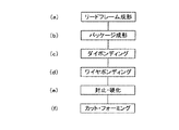
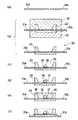
【解決手段】多数の半導体発光素子が搭載されたリードフレーム1a、1bをインサートとして多数個取りの金型5に挿入して密閉し、金型内にキャビティ6とLEDチップ2を包含する密閉空間7を形成する。そして、キャビティ6内に成形材料となる高反射率の非透光性樹脂を圧入して固化させ、その後、半導体発光素子が搭載された成形品を金型5から取り出して順次ワイヤボンディング及び半導体発光素子とボンディングワイヤの透光性樹脂による封止の工程を経て完成する。
【選択図】 図2
Description
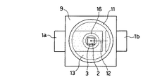
2 LEDチップ
3 接合部材
4 パーティングメン
5 金型
6 キャビティ
7 密閉空間
8 パッケージ
9 ランプハウス
10 凹部
11 反射面
12 ボンディングワイヤ
13 透光性樹脂
14 光出射面
15 凹部
16 反射面
17 端面
Claims (3)
- ランプハウスに設けられた擂鉢形状の凹部の底部に配置されたリードフレームに半導体発光素子がダイボンディングされ、前記半導体発光素子に設けられた電極と前記半導体発光素子がダイボンディングされたリードフレームとは分離した前記凹部の底部に配置されたリードフレームがボンディングワイヤによって接続され、前記凹部内に充填された透光性樹脂によって前記半導体発光素子及び前記ボンディングワイヤが封止されている半導体発光装置の製造方法であって、前記リードフレームを形成する第1の工程と、前記リードフレームに前記半導体発光素子をダイボンディングする第2の工程と、前記リードフレームと前記ランプハウスを一体形成する第3の工程と、前記半導体発光素子に設けられた電極と前記半導体発光素子がダイボンディングされたリードフレームとは分離したリードフレームをボンディングワイヤを介して接続するためにワイヤボンディングする第4の工程と、前記半導体発光素子と前記ボンディングワイヤを透光性樹脂で封止する第5の工程とを有することを特徴とする半導体発光装置の製造方法。
- 前記第3の工程において、前記リードフレームにダイボンディングされた前記半導体発光素子が前記ランプハウスを形成する成形材料に埋没しないように、且つ成形材料から発生するガスに汚染されないように前記半導体発光素子に保護手段を施したことを特徴とする請求項1に記載の半導体発光装置の製造方法。
- 前記保護手段は前記半導体発光素子を包含する密閉空間を形成したことであることを特徴とする請求1または2の何れか1項に記載の半導体発光装置の製造方法。
Priority Applications (1)
| Application Number | Priority Date | Filing Date | Title |
|---|---|---|---|
| JP2004111120A JP2005294736A (ja) | 2004-04-05 | 2004-04-05 | 半導体発光装置の製造方法 |
Applications Claiming Priority (1)
| Application Number | Priority Date | Filing Date | Title |
|---|---|---|---|
| JP2004111120A JP2005294736A (ja) | 2004-04-05 | 2004-04-05 | 半導体発光装置の製造方法 |
Publications (1)
| Publication Number | Publication Date |
|---|---|
| JP2005294736A true JP2005294736A (ja) | 2005-10-20 |
Family
ID=35327292
Family Applications (1)
| Application Number | Title | Priority Date | Filing Date |
|---|---|---|---|
| JP2004111120A Pending JP2005294736A (ja) | 2004-04-05 | 2004-04-05 | 半導体発光装置の製造方法 |
Country Status (1)
| Country | Link |
|---|---|
| JP (1) | JP2005294736A (ja) |
Cited By (36)
| Publication number | Priority date | Publication date | Assignee | Title |
|---|---|---|---|---|
| JP2007188059A (ja) * | 2005-12-12 | 2007-07-26 | Nichia Chem Ind Ltd | 光部品、光変換部材及び発光装置 |
| JP2007280983A (ja) * | 2006-04-03 | 2007-10-25 | Nichia Chem Ind Ltd | 発光装置 |
| JP2008053726A (ja) * | 2006-08-23 | 2008-03-06 | Seoul Semiconductor Co Ltd | 発光ダイオードパッケージ |
| JP2008098218A (ja) * | 2006-05-10 | 2008-04-24 | Nichia Chem Ind Ltd | 半導体発光装置及び半導体発光装置の製造方法 |
| WO2008072862A1 (en) * | 2006-12-13 | 2008-06-19 | Seoul Semiconductor Co., Ltd. | Light emitting diode package with odds of lead fram removed from its surface and method for fabricating the same |
| WO2008081696A1 (ja) | 2006-12-28 | 2008-07-10 | Nichia Corporation | 発光装置、パッケージ、発光装置の製造方法、パッケージの製造方法及びパッケージ製造用金型 |
| WO2008081794A1 (ja) | 2006-12-28 | 2008-07-10 | Nichia Corporation | 発光装置およびその製造方法 |
| KR100855062B1 (ko) | 2007-06-26 | 2008-08-29 | 럭스피아(주) | 발광 다이오드 패키지 및 그 제조 방법 |
| WO2008123232A1 (ja) * | 2007-03-30 | 2008-10-16 | Rohm Co., Ltd. | 半導体発光装置 |
| JP2010040791A (ja) * | 2008-08-05 | 2010-02-18 | Nichia Corp | 光半導体装置 |
| US7696525B2 (en) | 2006-04-21 | 2010-04-13 | Samsung Electro-Mechanics Co., Ltd. | Surface mounting device-type light emitting diode |
| KR100956888B1 (ko) | 2008-01-24 | 2010-05-11 | 삼성전기주식회사 | 발광 다이오드 패키지 및 그 제조 방법 |
| JP2010165979A (ja) * | 2009-01-19 | 2010-07-29 | Rohm Co Ltd | Ledモジュールの製造方法およびledモジュール |
| JP2011035306A (ja) * | 2009-08-05 | 2011-02-17 | Sharp Corp | 発光装置および発光装置の製造方法 |
| JP2011508416A (ja) * | 2007-12-24 | 2011-03-10 | サムソン エルイーディー カンパニーリミテッド. | 発光ダイオードパッケージ |
| US7932525B2 (en) | 2007-05-29 | 2011-04-26 | Iwatani Corporation | Semiconductor light-emitting device |
| KR101099494B1 (ko) | 2010-11-19 | 2011-12-27 | (주)네오빛 | 발광다이오드 패키지 |
| CN102299240A (zh) * | 2010-06-28 | 2011-12-28 | 乐金显示有限公司 | 发光二极管以及包括其的背光单元和液晶显示器件 |
| JP2012510153A (ja) * | 2008-11-25 | 2012-04-26 | エルジー イノテック カンパニー リミテッド | 発光素子パッケージ |
| EP2124252A4 (en) * | 2007-03-09 | 2012-10-17 | Omron Tateisi Electronics Co | Package manufacturing method, package, optical module and die for integral molding |
| CN102767707A (zh) * | 2012-05-21 | 2012-11-07 | 王定锋 | 在导线线路板上直接形成led支架的led模组及其制造方法 |
| US8362512B2 (en) | 2006-04-24 | 2013-01-29 | Cree, Inc. | Side-view surface mount white LED |
| CN103022275A (zh) * | 2011-09-23 | 2013-04-03 | 展晶科技(深圳)有限公司 | 发光二极管的封装方法 |
| CN103117348A (zh) * | 2011-11-16 | 2013-05-22 | Lg伊诺特有限公司 | 发光器件以及具有发光器件的照明装置 |
| JP2013102175A (ja) * | 2012-12-25 | 2013-05-23 | Nichia Chem Ind Ltd | 光半導体装置 |
| US8617909B2 (en) | 2004-07-02 | 2013-12-31 | Cree, Inc. | LED with substrate modifications for enhanced light extraction and method of making same |
| JP2014132688A (ja) * | 2014-03-25 | 2014-07-17 | Apic Yamada Corp | Ledパッケージ用基板、ledパッケージ用基板の製造方法、及び、ledパッケージの製造方法 |
| US8802459B2 (en) | 2006-12-28 | 2014-08-12 | Nichia Corporation | Surface mount lateral light emitting apparatus and fabrication method thereof |
| EP2383808A3 (en) * | 2010-04-30 | 2014-08-27 | Nichia Corporation | Light emitting device package having leads with a recess for the chip mount area |
| US8858004B2 (en) | 2005-12-22 | 2014-10-14 | Cree, Inc. | Lighting device |
| US8901585B2 (en) | 2003-05-01 | 2014-12-02 | Cree, Inc. | Multiple component solid state white light |
| US9431589B2 (en) | 2007-12-14 | 2016-08-30 | Cree, Inc. | Textured encapsulant surface in LED packages |
| US9666772B2 (en) | 2003-04-30 | 2017-05-30 | Cree, Inc. | High powered light emitter packages with compact optics |
| US10096756B2 (en) | 2005-11-25 | 2018-10-09 | Samsung Electronics Co., Ltd. | Side view light emitting diode package |
| US10615324B2 (en) | 2013-06-14 | 2020-04-07 | Cree Huizhou Solid State Lighting Company Limited | Tiny 6 pin side view surface mount LED |
| JP2022126390A (ja) * | 2021-02-18 | 2022-08-30 | 日亜化学工業株式会社 | 発光装置及びその製造方法 |
-
2004
- 2004-04-05 JP JP2004111120A patent/JP2005294736A/ja active Pending
Cited By (54)
| Publication number | Priority date | Publication date | Assignee | Title |
|---|---|---|---|---|
| US9666772B2 (en) | 2003-04-30 | 2017-05-30 | Cree, Inc. | High powered light emitter packages with compact optics |
| US8901585B2 (en) | 2003-05-01 | 2014-12-02 | Cree, Inc. | Multiple component solid state white light |
| US8617909B2 (en) | 2004-07-02 | 2013-12-31 | Cree, Inc. | LED with substrate modifications for enhanced light extraction and method of making same |
| US10096756B2 (en) | 2005-11-25 | 2018-10-09 | Samsung Electronics Co., Ltd. | Side view light emitting diode package |
| JP2007188059A (ja) * | 2005-12-12 | 2007-07-26 | Nichia Chem Ind Ltd | 光部品、光変換部材及び発光装置 |
| US8858004B2 (en) | 2005-12-22 | 2014-10-14 | Cree, Inc. | Lighting device |
| JP2007280983A (ja) * | 2006-04-03 | 2007-10-25 | Nichia Chem Ind Ltd | 発光装置 |
| US7696525B2 (en) | 2006-04-21 | 2010-04-13 | Samsung Electro-Mechanics Co., Ltd. | Surface mounting device-type light emitting diode |
| US8487337B2 (en) | 2006-04-24 | 2013-07-16 | Cree, Inc. | Side view surface mount LED |
| US8362512B2 (en) | 2006-04-24 | 2013-01-29 | Cree, Inc. | Side-view surface mount white LED |
| JP2008098218A (ja) * | 2006-05-10 | 2008-04-24 | Nichia Chem Ind Ltd | 半導体発光装置及び半導体発光装置の製造方法 |
| JP2008053726A (ja) * | 2006-08-23 | 2008-03-06 | Seoul Semiconductor Co Ltd | 発光ダイオードパッケージ |
| US7999280B2 (en) | 2006-08-23 | 2011-08-16 | Seoul Semiconductor Co., Ltd. | Light emitting diode package employing lead terminal with reflecting surface |
| WO2008072862A1 (en) * | 2006-12-13 | 2008-06-19 | Seoul Semiconductor Co., Ltd. | Light emitting diode package with odds of lead fram removed from its surface and method for fabricating the same |
| US8440478B2 (en) | 2006-12-28 | 2013-05-14 | Nichia Corporation | Light emitting device, package, light emitting device manufacturing method, package manufacturing method and package manufacturing die |
| US8217414B2 (en) | 2006-12-28 | 2012-07-10 | Nichia Corporation | Light emitting device, package, light emitting device manufacturing method, package manufacturing method and package manufacturing die |
| US8802459B2 (en) | 2006-12-28 | 2014-08-12 | Nichia Corporation | Surface mount lateral light emitting apparatus and fabrication method thereof |
| WO2008081696A1 (ja) | 2006-12-28 | 2008-07-10 | Nichia Corporation | 発光装置、パッケージ、発光装置の製造方法、パッケージの製造方法及びパッケージ製造用金型 |
| WO2008081794A1 (ja) | 2006-12-28 | 2008-07-10 | Nichia Corporation | 発光装置およびその製造方法 |
| US8093619B2 (en) | 2006-12-28 | 2012-01-10 | Nichia Corporation | Light emitting device |
| US9190588B2 (en) | 2006-12-28 | 2015-11-17 | Nichia Corporation | Side-view type light emitting apparatus and package |
| EP2124252A4 (en) * | 2007-03-09 | 2012-10-17 | Omron Tateisi Electronics Co | Package manufacturing method, package, optical module and die for integral molding |
| US8334548B2 (en) | 2007-03-30 | 2012-12-18 | Rohm Co., Ltd. | Semiconductor light emitting device |
| WO2008123232A1 (ja) * | 2007-03-30 | 2008-10-16 | Rohm Co., Ltd. | 半導体発光装置 |
| US7932525B2 (en) | 2007-05-29 | 2011-04-26 | Iwatani Corporation | Semiconductor light-emitting device |
| KR100855062B1 (ko) | 2007-06-26 | 2008-08-29 | 럭스피아(주) | 발광 다이오드 패키지 및 그 제조 방법 |
| US9431589B2 (en) | 2007-12-14 | 2016-08-30 | Cree, Inc. | Textured encapsulant surface in LED packages |
| JP2011508416A (ja) * | 2007-12-24 | 2011-03-10 | サムソン エルイーディー カンパニーリミテッド. | 発光ダイオードパッケージ |
| KR100956888B1 (ko) | 2008-01-24 | 2010-05-11 | 삼성전기주식회사 | 발광 다이오드 패키지 및 그 제조 방법 |
| JP2010040791A (ja) * | 2008-08-05 | 2010-02-18 | Nichia Corp | 光半導体装置 |
| EP2899762A1 (en) * | 2008-11-25 | 2015-07-29 | LG Innotek Co., Ltd. | Light emitting device package |
| JP2014241443A (ja) * | 2008-11-25 | 2014-12-25 | エルジー イノテック カンパニー リミテッド | 発光素子パッケージ |
| US10847680B2 (en) | 2008-11-25 | 2020-11-24 | Lg Innotek Co., Ltd. | Light emitting device package |
| US10134953B2 (en) | 2008-11-25 | 2018-11-20 | Lg Innotek Co., Ltd. | Light-emitting device package including lead frame and using lead terminal as a reflective cavity |
| JP2012510153A (ja) * | 2008-11-25 | 2012-04-26 | エルジー イノテック カンパニー リミテッド | 発光素子パッケージ |
| US9425360B2 (en) | 2008-11-25 | 2016-08-23 | Lg Innotek Co., Ltd. | Light emitting device package |
| US8928008B2 (en) | 2008-11-25 | 2015-01-06 | Lg Innotek Co., Ltd. | Light emitting device package comprising a lead electrode exposed to a recessed bottom portion of the package body |
| JP2010165979A (ja) * | 2009-01-19 | 2010-07-29 | Rohm Co Ltd | Ledモジュールの製造方法およびledモジュール |
| JP2011035306A (ja) * | 2009-08-05 | 2011-02-17 | Sharp Corp | 発光装置および発光装置の製造方法 |
| EP2383808A3 (en) * | 2010-04-30 | 2014-08-27 | Nichia Corporation | Light emitting device package having leads with a recess for the chip mount area |
| CN102299240B (zh) * | 2010-06-28 | 2014-06-18 | 乐金显示有限公司 | 发光二极管以及包括其的背光单元和液晶显示器件 |
| CN102299240A (zh) * | 2010-06-28 | 2011-12-28 | 乐金显示有限公司 | 发光二极管以及包括其的背光单元和液晶显示器件 |
| US8625053B2 (en) | 2010-06-28 | 2014-01-07 | Lg Display Co., Ltd. | Light emitting diode and backlight unit and liquid crystal display device with the same |
| KR101099494B1 (ko) | 2010-11-19 | 2011-12-27 | (주)네오빛 | 발광다이오드 패키지 |
| TWI455367B (zh) * | 2011-09-23 | 2014-10-01 | Advanced Optoelectronic Tech | 發光二極體的封裝方法 |
| CN103022275A (zh) * | 2011-09-23 | 2013-04-03 | 展晶科技(深圳)有限公司 | 发光二极管的封装方法 |
| CN103117348A (zh) * | 2011-11-16 | 2013-05-22 | Lg伊诺特有限公司 | 发光器件以及具有发光器件的照明装置 |
| US10128423B2 (en) | 2011-11-16 | 2018-11-13 | Lg Innotek Co., Ltd. | Light emitting device and lighting apparatus having the same |
| CN102767707A (zh) * | 2012-05-21 | 2012-11-07 | 王定锋 | 在导线线路板上直接形成led支架的led模组及其制造方法 |
| JP2013102175A (ja) * | 2012-12-25 | 2013-05-23 | Nichia Chem Ind Ltd | 光半導体装置 |
| US10615324B2 (en) | 2013-06-14 | 2020-04-07 | Cree Huizhou Solid State Lighting Company Limited | Tiny 6 pin side view surface mount LED |
| JP2014132688A (ja) * | 2014-03-25 | 2014-07-17 | Apic Yamada Corp | Ledパッケージ用基板、ledパッケージ用基板の製造方法、及び、ledパッケージの製造方法 |
| JP2022126390A (ja) * | 2021-02-18 | 2022-08-30 | 日亜化学工業株式会社 | 発光装置及びその製造方法 |
| JP7549220B2 (ja) | 2021-02-18 | 2024-09-11 | 日亜化学工業株式会社 | 発光装置及びその製造方法 |
Similar Documents
| Publication | Publication Date | Title |
|---|---|---|
| JP2005294736A (ja) | 半導体発光装置の製造方法 | |
| CN100452380C (zh) | 表面安装型半导体器件及其引线架结构 | |
| EP2218116B1 (en) | Slim led package | |
| CN103718314B (zh) | 发光装置 | |
| CN102939669B (zh) | 可表面安装的光电子器件和用于制造可表面安装的光电子器件的方法 | |
| US20060273337A1 (en) | Side-emitting LED package and method of manufacturing the same | |
| US20130037845A1 (en) | Lead frame, and light emitting diode module having the same | |
| US8530252B2 (en) | Method for manufacturing light emitting diode | |
| KR20050092300A (ko) | 고출력 발광 다이오드 패키지 | |
| TWI713437B (zh) | 發光組件及其製造方法 | |
| JP2018160677A (ja) | 半導体発光装置 | |
| JP2005317661A (ja) | 半導体発光装置およびその製造方法 | |
| JP4976168B2 (ja) | 発光装置 | |
| CN103378268A (zh) | 封装件和封装件的制造方法 | |
| JP3219881U (ja) | 発光素子パッケージ | |
| JP2007329516A (ja) | 半導体発光装置 | |
| JP2012109521A (ja) | Ledモジュール装置及びその製造方法 | |
| US20130343068A1 (en) | Light emitting device package, and display apparatus and lighting system having the same | |
| JP2008147203A (ja) | 半導体発光装置 | |
| JP2012049486A (ja) | Ledパッケージとその製造方法、及び該ledパッケージを用いて構成したledモジュール装置とその製造方法 | |
| KR100585014B1 (ko) | 일체형 열전달 슬러그가 형성된 발광다이오드 패키지 및 그 제조방법 | |
| JP2005116937A (ja) | 半導体発光装置およびその製造方法 | |
| CN100481430C (zh) | 表面安装型发光二极管 | |
| JP2006049624A (ja) | 発光素子 | |
| JP2005217308A (ja) | 半導体発光装置及びその製法 |
Legal Events
| Date | Code | Title | Description |
|---|---|---|---|
| A621 | Written request for application examination |
Free format text: JAPANESE INTERMEDIATE CODE: A621 Effective date: 20070220 |
|
| A131 | Notification of reasons for refusal |
Free format text: JAPANESE INTERMEDIATE CODE: A131 Effective date: 20090721 |
|
| A977 | Report on retrieval |
Free format text: JAPANESE INTERMEDIATE CODE: A971007 Effective date: 20090721 |
|
| A521 | Request for written amendment filed |
Free format text: JAPANESE INTERMEDIATE CODE: A523 Effective date: 20090910 |
|
| A02 | Decision of refusal |
Free format text: JAPANESE INTERMEDIATE CODE: A02 Effective date: 20091124 |