JP2005294736A - Manufacturing method of semiconductor light emitting device - Google Patents
Manufacturing method of semiconductor light emitting device Download PDFInfo
- Publication number
- JP2005294736A JP2005294736A JP2004111120A JP2004111120A JP2005294736A JP 2005294736 A JP2005294736 A JP 2005294736A JP 2004111120 A JP2004111120 A JP 2004111120A JP 2004111120 A JP2004111120 A JP 2004111120A JP 2005294736 A JP2005294736 A JP 2005294736A
- Authority
- JP
- Japan
- Prior art keywords
- semiconductor light
- light emitting
- lead frame
- emitting element
- manufacturing
- Prior art date
- Legal status (The legal status is an assumption and is not a legal conclusion. Google has not performed a legal analysis and makes no representation as to the accuracy of the status listed.)
- Pending
Links
Images
Classifications
-
- H—ELECTRICITY
- H10—SEMICONDUCTOR DEVICES; ELECTRIC SOLID-STATE DEVICES NOT OTHERWISE PROVIDED FOR
- H10W—GENERIC PACKAGES, INTERCONNECTIONS, CONNECTORS OR OTHER CONSTRUCTIONAL DETAILS OF DEVICES COVERED BY CLASS H10
- H10W72/00—Interconnections or connectors in packages
- H10W72/071—Connecting or disconnecting
- H10W72/073—Connecting or disconnecting of die-attach connectors
-
- H—ELECTRICITY
- H10—SEMICONDUCTOR DEVICES; ELECTRIC SOLID-STATE DEVICES NOT OTHERWISE PROVIDED FOR
- H10W—GENERIC PACKAGES, INTERCONNECTIONS, CONNECTORS OR OTHER CONSTRUCTIONAL DETAILS OF DEVICES COVERED BY CLASS H10
- H10W72/00—Interconnections or connectors in packages
- H10W72/071—Connecting or disconnecting
- H10W72/075—Connecting or disconnecting of bond wires
-
- H—ELECTRICITY
- H10—SEMICONDUCTOR DEVICES; ELECTRIC SOLID-STATE DEVICES NOT OTHERWISE PROVIDED FOR
- H10W—GENERIC PACKAGES, INTERCONNECTIONS, CONNECTORS OR OTHER CONSTRUCTIONAL DETAILS OF DEVICES COVERED BY CLASS H10
- H10W72/00—Interconnections or connectors in packages
- H10W72/50—Bond wires
- H10W72/531—Shapes of wire connectors
- H10W72/536—Shapes of wire connectors the connected ends being ball-shaped
-
- H—ELECTRICITY
- H10—SEMICONDUCTOR DEVICES; ELECTRIC SOLID-STATE DEVICES NOT OTHERWISE PROVIDED FOR
- H10W—GENERIC PACKAGES, INTERCONNECTIONS, CONNECTORS OR OTHER CONSTRUCTIONAL DETAILS OF DEVICES COVERED BY CLASS H10
- H10W72/00—Interconnections or connectors in packages
- H10W72/50—Bond wires
- H10W72/531—Shapes of wire connectors
- H10W72/5363—Shapes of wire connectors the connected ends being wedge-shaped
-
- H—ELECTRICITY
- H10—SEMICONDUCTOR DEVICES; ELECTRIC SOLID-STATE DEVICES NOT OTHERWISE PROVIDED FOR
- H10W—GENERIC PACKAGES, INTERCONNECTIONS, CONNECTORS OR OTHER CONSTRUCTIONAL DETAILS OF DEVICES COVERED BY CLASS H10
- H10W72/00—Interconnections or connectors in packages
- H10W72/851—Dispositions of multiple connectors or interconnections
- H10W72/874—On different surfaces
- H10W72/884—Die-attach connectors and bond wires
-
- H—ELECTRICITY
- H10—SEMICONDUCTOR DEVICES; ELECTRIC SOLID-STATE DEVICES NOT OTHERWISE PROVIDED FOR
- H10W—GENERIC PACKAGES, INTERCONNECTIONS, CONNECTORS OR OTHER CONSTRUCTIONAL DETAILS OF DEVICES COVERED BY CLASS H10
- H10W74/00—Encapsulations, e.g. protective coatings
-
- H—ELECTRICITY
- H10—SEMICONDUCTOR DEVICES; ELECTRIC SOLID-STATE DEVICES NOT OTHERWISE PROVIDED FOR
- H10W—GENERIC PACKAGES, INTERCONNECTIONS, CONNECTORS OR OTHER CONSTRUCTIONAL DETAILS OF DEVICES COVERED BY CLASS H10
- H10W90/00—Package configurations
- H10W90/701—Package configurations characterised by the relative positions of pads or connectors relative to package parts
- H10W90/731—Package configurations characterised by the relative positions of pads or connectors relative to package parts of die-attach connectors
- H10W90/736—Package configurations characterised by the relative positions of pads or connectors relative to package parts of die-attach connectors between a chip and a stacked lead frame, conducting package substrate or heat sink
-
- H—ELECTRICITY
- H10—SEMICONDUCTOR DEVICES; ELECTRIC SOLID-STATE DEVICES NOT OTHERWISE PROVIDED FOR
- H10W—GENERIC PACKAGES, INTERCONNECTIONS, CONNECTORS OR OTHER CONSTRUCTIONAL DETAILS OF DEVICES COVERED BY CLASS H10
- H10W90/00—Package configurations
- H10W90/701—Package configurations characterised by the relative positions of pads or connectors relative to package parts
- H10W90/751—Package configurations characterised by the relative positions of pads or connectors relative to package parts of bond wires
- H10W90/756—Package configurations characterised by the relative positions of pads or connectors relative to package parts of bond wires between a chip and a stacked lead frame, conducting package substrate or heat sink
Landscapes
- Led Device Packages (AREA)
Abstract
【課題】本発明は、リードフレームとランプハウスが一体形成されたパッケージに半導体発光素子を搭載した表面実装型の半導体発光装置において、光取り出し効率及び光の利用効率を高めて高輝度の半導体発光装置を実現する製造方法を提供する。
【解決手段】多数の半導体発光素子が搭載されたリードフレーム1a、1bをインサートとして多数個取りの金型5に挿入して密閉し、金型内にキャビティ6とLEDチップ2を包含する密閉空間7を形成する。そして、キャビティ6内に成形材料となる高反射率の非透光性樹脂を圧入して固化させ、その後、半導体発光素子が搭載された成形品を金型5から取り出して順次ワイヤボンディング及び半導体発光素子とボンディングワイヤの透光性樹脂による封止の工程を経て完成する。
【選択図】 図2The present invention relates to a surface-mount type semiconductor light-emitting device in which a semiconductor light-emitting element is mounted on a package in which a lead frame and a lamp house are integrally formed. A manufacturing method for realizing the apparatus is provided.
A lead frame (1a, 1b) on which a large number of semiconductor light emitting elements are mounted is inserted into a multi-piece mold (5) and sealed, and a sealed space including a cavity (6) and an LED chip (2) in the mold. 7 is formed. Then, a highly reflective non-translucent resin as a molding material is press-fitted into the cavity 6 to solidify, and thereafter, a molded product on which the semiconductor light emitting element is mounted is taken out from the mold 5 and sequentially wire bonded and semiconductor light emitting. The element and the bonding wire are completed through a sealing process using a translucent resin.
[Selection] Figure 2
Description
本発明は、半導体発光装置の製造方法に関するものであり、詳しくはリードフレームを使用した表面実装型の半導体発光装置の製造方法に関する。 The present invention relates to a method for manufacturing a semiconductor light emitting device, and more particularly to a method for manufacturing a surface mount type semiconductor light emitting device using a lead frame.
発光ダイオード(LED)はプリント基板に実装するときの実装方法によって二種類に大別することができる。一種は両面スルーホールプリント基板のスルーホールにLEDチップが搭載されたリードフレームを挿入してプリント基板の反対側から半田付けによって固定するものであり、他の一種はプリント基板上にLEDを配置して同一面上に形成された回路導体パターンに電極を半田付けして固定するものである。 Light emitting diodes (LEDs) can be broadly classified into two types depending on the mounting method when mounted on a printed board. One type is to insert a lead frame with an LED chip into the through hole of the double-sided through-hole printed circuit board and fix it by soldering from the opposite side of the printed circuit board. The other type is to place the LED on the printed circuit board. Then, the electrodes are soldered and fixed to the circuit conductor pattern formed on the same surface.
後者は表面実装型LEDと呼ばれ、片面のみに回路導体パターンを設けたプリント基板が採用できるためにコストダウンに寄与する半導体発光装置となる。また、一般的に前者に比べて著しく小型化が進んでおり、現在では携帯電話、PDAなどの小型機器を構成する液晶やテンキー等の照明用光源、カメラ付携帯電話の補助光源やストロボ用光源等として使用されている。 The latter is called a surface-mounted LED, and a semiconductor light-emitting device that contributes to cost reduction is possible because a printed circuit board provided with a circuit conductor pattern only on one side can be adopted. In general, the size has been remarkably reduced compared to the former. At present, light sources for illumination such as liquid crystal and numeric keys, etc. constituting small devices such as mobile phones and PDAs, auxiliary light sources for camera-equipped mobile phones and light sources for strobes are used. Etc. are used.
また、表面実装型LEDの構造は二種類に大別でき、一種はプリント基板に形成された回路導体パターンに共晶接合或いは半田接合等の接合方法でLEDチップを固定(ダイボンディング)することによってLEDチップの下方の電極と回路導体パターンとの電気的導通を図り、LEDチップの上方の電極とLEDチップが固定された回路導体パターンとは分離した回路導体パターンをボンディングワイヤを介して接続(ワイヤボンディング)することによって電気的導通を図り、前記LEDチップ及びボンディングワイヤを透光性樹脂で封止することによってLEDチップを水分、塵埃及びガス等の外部環境から保護し、且つボンディングワイヤを振動及び衝撃等の機械的応力から保護したものである。 In addition, the structure of surface-mounted LEDs can be broadly divided into two types. One type is by fixing (die bonding) LED chips to a circuit conductor pattern formed on a printed circuit board by a bonding method such as eutectic bonding or solder bonding. The electrical connection between the lower electrode of the LED chip and the circuit conductor pattern is achieved, and the upper electrode electrode of the LED chip and the circuit conductive pattern separated from the circuit conductive pattern to which the LED chip is fixed are connected via a bonding wire (wire The LED chip and the bonding wire are sealed with a translucent resin to protect the LED chip from the external environment such as moisture, dust and gas, and the bonding wire is vibrated and It is protected from mechanical stress such as impact.
他の一種は略平板状のリードフレームが擂鉢形状の凹部が形成された高反射率を有する非透光性樹脂からなるランプハウスに埋め込まれて一体形成されてパッケージが構成され、前記パッケージのランプハウスの凹部の底部に露出したリードフレームに共晶接合或いは半田接合等の接合方法でLEDチップをダイボンディングすることによってLEDチップの下方の電極とリードフレームとの電気的導通を図り、LEDチップの上方の電極とLEDチップがダイボンディングされたリードフレームとは分離したリードフレームをワイヤボンディングすることによってボンディングワイヤを介して接続して電気的導通を図り、凹部内に透光性樹脂を充填することによってLEDチップ及びボンディングワイヤを封止したものである。 Another type is a substantially flat lead frame embedded in a lamp house made of a non-translucent resin having a high reflectivity in which a bowl-shaped recess is formed to form a package, and the lamp of the package The LED chip is die-bonded to the lead frame exposed at the bottom of the recess of the house by a bonding method such as eutectic bonding or solder bonding, thereby achieving electrical conduction between the electrode under the LED chip and the lead frame. The lead frame separated from the upper electrode and the lead frame to which the LED chip is die-bonded is connected by wire bonding to achieve electrical continuity, and the recess is filled with a translucent resin. The LED chip and the bonding wire are sealed.
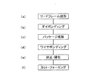
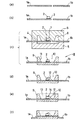
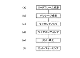
なお、後者の表面実装型LEDの従来の製造方法は、図6(a)及び図7(a)のリードフレーム31a、31bを成形する工程、図6(b)及び図7(b)の成形金型32にリードフレーム31a、31bを埋め込んでセットし、高反射率の非透光性樹脂をキャビティ40に圧入してリードフレーム31a、31bとランプハウス33が一体形成されたパッケージ34に成形する工程、図6(c)及び図7(c)のパッケージのランプハウス33に形成された凹部35の底部のリードフレーム31a上に接合部材39を介してLEDチップ36を搭載するダイボンディング工程、図6(d)及び図7(d)のダイボンディングされたLEDチップ36の上方電極とリードフレーム31bをボンディングワイヤ37で接続するワイヤボンディング工程、図6(e)及び図7(e)のパッケージのランプハウス33の凹部35内に透光性樹脂38を充填、硬化してLEDチップ36及びボンディングワイヤ37を封止する工程、図6(f)及び図7(f)のリードフレーム31a、31bをカット・フォーミングする工程を順次経て製造されるものである(例えば、特許文献1参照。)。
しかしながら、上述した従来の表面実装型LEDの製造方法は、LEDチップをリードフレームに共晶接合或いは半田接合等の接合方法でダイボンディングする際の高温環境下でパッケージの非透光性樹脂からなるランプハウスに変形や焦げを生じ易いという問題を有している。 However, the conventional method for manufacturing a surface-mounted LED described above is made of a non-translucent resin for a package in a high-temperature environment when the LED chip is die-bonded to a lead frame by a bonding method such as eutectic bonding or solder bonding. There is a problem that the lamp house is likely to be deformed or burnt.
一方、この問題を回避するために共晶接合時或いは半田接合時の高温環境下に耐えられる非透光性樹脂をランプハウスを形成する材料として採用することが考えられるが、その場合は採用する樹脂の選択範囲が限定され、高反射率の非透光性樹脂であっても耐熱性が低いために採用できない場合が生じ、その結果、満足するような優れた光学特性の製品を作り上げることができないことになる。 On the other hand, in order to avoid this problem, it is conceivable to use a non-translucent resin that can withstand a high temperature environment during eutectic bonding or solder bonding as a material for forming the lamp house. The selection range of the resin is limited, and even if it is a non-transparent resin with high reflectivity, it may not be adopted due to low heat resistance, and as a result, a product with excellent optical characteristics to satisfy can be created It will not be possible.
従って、従来の表面実装型LEDの製造方法は、共晶接合及び半田接合等の接合方法でLEDチップをリードフレームにダイボンディングするには適した方法であるとは言い難いものである。 Therefore, it is difficult to say that a conventional method for manufacturing a surface-mounted LED is a method suitable for die-bonding an LED chip to a lead frame by a bonding method such as eutectic bonding or solder bonding.
そこで、本発明は上記問題に鑑みて創案なされたもので、光の利用効率を高くして高輝度化された表面実装型LEDの製造方法を提供するものである。 Accordingly, the present invention has been made in view of the above-described problems, and provides a method for manufacturing a surface-mounted LED with high light use efficiency and high brightness.
上記課題を解決するために、本発明の請求項1に記載された発明は、ランプハウスに設けられた擂鉢形状の凹部の底部に配置されたリードフレームに半導体発光素子がダイボンディングされ、前記半導体発光素子に設けられた電極と前記半導体発光素子がダイボンディングされたリードフレームとは分離した前記凹部の底部に配置されたリードフレームがボンディングワイヤによって接続され、前記凹部内に充填された透光性樹脂によって前記半導体発光素子及び前記ボンディングワイヤが封止されている半導体発光装置の製造方法であって、前記リードフレームを形成する第1の工程と、前記リードフレームに前記半導体発光素子をダイボンディングする第2の工程と、前記リードフレームと前記ランプハウスを一体形成する第3の工程と、前記半導体発光素子に設けられた電極と前記半導体発光素子がダイボンディングされたリードフレームとは分離したリードフレームをボンディングワイヤを介して接続するためにワイヤボンディングする第4の工程と、前記半導体発光素子と前記ボンディングワイヤを透光性樹脂で封止する第5の工程とを有することを特徴とするものである。 In order to solve the above-mentioned problems, according to a first aspect of the present invention, a semiconductor light-emitting element is die-bonded to a lead frame arranged at the bottom of a bowl-shaped recess provided in a lamp house, and the semiconductor A lead frame disposed at the bottom of the recess separated from the electrode provided on the light emitting element and the lead frame to which the semiconductor light emitting element is die-bonded is connected by a bonding wire, and the translucency filled in the recess A method of manufacturing a semiconductor light emitting device in which the semiconductor light emitting element and the bonding wire are sealed with a resin, the first step of forming the lead frame, and die bonding of the semiconductor light emitting element to the lead frame A second step, and a third step of integrally forming the lead frame and the lamp house; A fourth step of wire bonding in order to connect a lead frame separated from an electrode provided on the semiconductor light emitting device and a lead frame to which the semiconductor light emitting device is die-bonded via a bonding wire; and the semiconductor light emitting device And a fifth step of sealing the bonding wire with a translucent resin.
また、本発明の請求項2に記載された発明は、請求項1の前記第3の工程において、前記リードフレームにダイボンディングされた前記半導体発光素子が前記ランプハウスを形成する成形材料に埋没しないように、且つ成形材料から発生するガスに汚染されないように前記半導体発光素子に保護手段を施したことを特徴とするものである。 According to a second aspect of the present invention, in the third step of the first aspect, the semiconductor light emitting element die-bonded to the lead frame is not buried in the molding material forming the lamp house. Thus, the semiconductor light emitting device is provided with a protection means so as not to be contaminated by the gas generated from the molding material.
また、本発明の請求項3に記載された発明は、請求項1または2の何れか1項において、前記保護手段は前記半導体発光素子を包含する密閉空間を形成したことであることを特徴とするものである。
In addition, the invention described in
リードフレームに半導体発光素子を搭載した後にリードフレームとランプハウスを一体形成することにより、ランプハウスがリードフレームに半導体発光素子を搭載するときの高温環境下に曝されることがないため、ランプハウスを形成する高反射率の成形材料を高耐熱性の拘束なく選択・採用することができるという利点がある。 By forming the lead frame and the lamp house integrally after mounting the semiconductor light emitting element on the lead frame, the lamp house is not exposed to the high temperature environment when mounting the semiconductor light emitting element on the lead frame. There is an advantage that a molding material having high reflectivity for forming can be selected and adopted without high heat resistance.
以下、この発明の好適な実施形態を図1から図5を参照しながら、詳細に説明する(同一部分については同じ符号を付す)。尚、以下に述べる実施形態は、本発明の好適な具体例であるから、技術的に好ましい種々の限定が付されているが、本発明の範囲は、以下の説明において特に本発明を限定する旨の記載がない限り、これらの態様に限られるものではない。 Hereinafter, preferred embodiments of the present invention will be described in detail with reference to FIG. 1 to FIG. 5 (the same parts are given the same reference numerals). The embodiments described below are preferable specific examples of the present invention, and thus various technically preferable limitations are given. However, the scope of the present invention particularly limits the present invention in the following description. As long as there is no description of the effect, it is not restricted to these aspects.
図1は本発明の半導体発光装置の製造方法に係わる工程フローチャート、図2は同じく半導体発光装置の製造方法に係わる工程図である。以降、図1と図2を対比しながら製造工程の詳細な説明を行う。 FIG. 1 is a process flowchart relating to a method for manufacturing a semiconductor light emitting device of the present invention, and FIG. Hereinafter, the manufacturing process will be described in detail while comparing FIG. 1 and FIG.
まず、図1(a)に示すように、リードフレームを形成する工程である。上述したように、本発明の表面実装型LEDは小型化の傾向が進んでおり、現状一例として縦・横とも3mm程度、高さが2mm程度の寸法で製品化されているものがある。このような小型の部品は量産開始から完成に至るまでの製造工程を1個単位で流すのではなく、多数個取りの状態で流して一括大量生産を行う場合がほとんどである。 First, as shown in FIG. 1A, a lead frame is formed. As described above, the surface-mount type LED of the present invention is being reduced in size, and as one example, there are some products that are manufactured in dimensions of about 3 mm in length and width and about 2 mm in height. In most cases, such small parts are not mass-produced by mass production from the start of mass production to completion, but in a single unit.
従って、リードフレームにおいても、多数のLEDチップが搭載できるように銅、鉄及び42アロイ系等の素材からなる一枚の金属板をプレス打抜き加工やエッチング手法によって所望する形状に形成し、金メッキ及び銀メッキ等の表面処理を行って図2(a)に示すようなリードフレーム1a、1bを成形する。
Therefore, in a lead frame, a single metal plate made of copper, iron, 42 alloy, or the like is formed into a desired shape by press punching or etching so that a large number of LED chips can be mounted. Surface treatment such as silver plating is performed to form
次に、図1(b)に示すダイボンディング工程である。これは、図2(b)に示すように、高温環境下での共晶接合や半田接合等の接合方法でLEDチップ2をリードフレーム1aに固定し、同時にLEDチップ2の下方電極とリードフレーム1aとを接合部材3を介して電気的導通を図る。
Next, a die bonding step shown in FIG. As shown in FIG. 2 (b), the
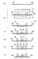
次に、図1(c)に示すパッケージ成形工程である。これは一般的には射出成形で行われ、図2(c)に示すようにリードフレーム1a、1bをインサートとして、リードフレーム1aのLEDチップ2が搭載された面をパーティング面4とする二つの多数個取りの金型5に挿入して密閉すると二つの金型5でキャビティ6が形成されると共に、リードフレーム1aに搭載されたLEDチップ2が成形材料に埋没しないように、また成形材料から発生するガスに汚染されないように二つの金型5とリードフレーム1aによってLEDチップ2を包含する密閉空間7が形成される。
Next, a package forming process shown in FIG. This is generally performed by injection molding. As shown in FIG. 2C, the
そして、上記インサートを挿入してセットが完了した金型5のキャビティ6内に成形材料となる高反射率の非透光性樹脂を圧入して固化させ、その後金型5から成形品を取り出すと図2(c)のような半導体発光装置のパッケージ8が出来上がる。
Then, a highly reflective non-transparent resin as a molding material is press-fitted into the
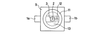
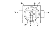
半導体発光装置のパッケージ8の高反射率の非透光性樹脂で成形されたランプハウス9は底部にLEDチップ2が配置された擂鉢形状の凹部10が形成され、その内周面は反射面11が形成されている。また、凹部10の底部に位置するリードフレーム1a、1bは表面が大気中に露出しており、表面を覆う物は何も存在しない。
The
次は図1(d)のワイヤボンディング工程である。これは図2(d)に示すように、LEDチップ2の上方電極と、LEDチップ2が搭載されたリードフレーム1aと分離したリードフレーム1bがランプハウス9の凹部10の底部に露出した部分とを金あるいはアルミニウムを主成分とする細線のボンディングワイヤ12によって接続し、両者の電気的導通を図ったものである。
Next is the wire bonding step of FIG. As shown in FIG. 2 (d), the upper electrode of the
次は図1(e)の封止・硬化工程である。これは図2(e)に示すように、ランプハウス9に形成された凹部10内にエポキシ樹脂あるいはシリコーン樹脂からなる透光性樹脂13を充填してLEDチップ2及びボンディングワイヤ12を封止し、硬化させる。
Next is the sealing / curing step of FIG. As shown in FIG. 2 (e), the
LEDチップ2とボンディングワイヤ12を透光性樹脂13で封止する目的の一つはLEDチップ2を水分、ガス及び塵埃などの外部環境から保護し、ボンディングワイヤ12を振動、衝撃などの機械的応力から保護することである。
One of the purposes of sealing the
同様に目的の一つは、エポキシ樹脂あるいはシリコーン樹脂からなる透光性樹脂13を透光性樹脂13と界面を形成するLEDチップ2の光出射面14を構成する半導体材料の屈折率に近い屈折率を有するものから選択・採用する。するとLEDチップ2内で発光した光のうち、LEDチップ2の光出射面14で全反射してLEDチップ2内に戻る光を極力少なくし、出来る限り多くの光をLEDチップ2の光出射面14から界面を形成する透光性樹脂13内に入射させてLEDチップ2からの光取り出し効率を高めることができるからである。
Similarly, one of the purposes is refraction close to the refractive index of the semiconductor material constituting the
そして最後は図1(f)に示すカット・フォーミングの工程である。これは、リードフレーム1a、1bによって連結された多数個の半導体発光装置のリードフレーム1a、1bをカットして個々の半導体発光装置に分離し、リードフレーム1a、1bを所望する形状にフォーミングするものである。図2(f)はリードフレームをフォーミングして完成した半導体発光装置の断面図であり、図3は図2(f)の上面図である。 Finally, the cutting and forming process shown in FIG. In this method, the lead frames 1a and 1b of a plurality of semiconductor light emitting devices connected by the lead frames 1a and 1b are cut and separated into individual semiconductor light emitting devices, and the lead frames 1a and 1b are formed into a desired shape. It is. FIG. 2F is a cross-sectional view of a semiconductor light emitting device completed by forming a lead frame, and FIG. 3 is a top view of FIG.
なお、ランプハウスを形成する樹脂に高反射率の部材を使用する効果は、半導体発光素子から発せられる光のうちランプハウスに形成された擂鉢形状の凹部の内周面方向に向かう光を内周面に形成された反射面で反射して半導体発光装置の放射方向に向け、集光効果によって光取り出し効率及び光の利用効率を高め、光源としての高輝度化を実現するものである。従って、凹部の内周面の反射率が高いほど光源の高輝度化が可能になる。 The effect of using a highly reflective member for the resin that forms the lamp house is that light emitted from the semiconductor light emitting element emits light directed toward the inner peripheral surface of the bowl-shaped recess formed in the lamp house. The light is reflected by the reflecting surface formed on the surface and directed in the radiation direction of the semiconductor light emitting device, and the light extraction efficiency and the light utilization efficiency are increased by the light condensing effect, thereby realizing high luminance as a light source. Therefore, the higher the reflectance of the inner peripheral surface of the recess, the higher the brightness of the light source.
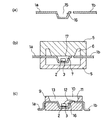
図4はリードフレームに内周面を反射面とする擂鉢形状の凹部を形成し、これを上記製造工程に投入して半導体発光装置を完成させるまでの工程を抜粋して表したもので、(a)は成形されたリードフレームの形状を示す断面図、(b)は半導体発光素子を搭載したリードフレームを金型にセットした状態を示す断面図、(c)完成品の断面図である。更に図5は図4(c)の完成品の上面図である。なお、ここではリードフレームを投入してから完成品に至るまでの製造工程は上記同様であるので全工程のなかから一部の工程図を記号を付して示し、同時に工程の説明は重複するので省略する。 FIG. 4 is an excerpt of the process from the formation of a bowl-shaped recess having an inner peripheral surface as a reflection surface on the lead frame, and the process up to the completion of the semiconductor light-emitting device. (a) is a cross-sectional view showing the shape of a molded lead frame, (b) is a cross-sectional view showing a state in which a lead frame on which a semiconductor light emitting element is mounted is set in a mold, and (c) is a cross-sectional view of a finished product. FIG. 5 is a top view of the finished product of FIG. Here, since the manufacturing process from the introduction of the lead frame to the finished product is the same as described above, some of the process drawings are shown with symbols, and the description of the process is duplicated at the same time. I will omit it.
この場合、リードフレームの凹部15内周面に形成された反射面16とランプハウス9の凹部10内周面に形成された反射面11が2段重ねで形成されており、反射面が一段のときに比べて反射面で反射される確率が高くなり、その分、光取り出し効率及び光の利用効率が高くなって、光源の高輝度化に繋がる。
In this case, the reflecting
また、リードフレーム1a、1bとランプハウス9を一体形成する場合、金型5によってリードフレーム1aの凹部15を覆うことによって密閉空間7が確保できるためにその中に包含された半導体発光素子2を確実に樹脂及び樹脂から発生するガスから保護することができる。更に、金型5の端面17を平面に形成することで密閉空間7が確実に確保できるために金型の製作コスト低減でき、その結果、製品コストも低減することができる。
Further, when the lead frames 1a and 1b and the
次に、本発明の半導体発光装置の製造方法の効果について説明する。まず、半導体発光素子がダイボンディングされたリードフレームを非透光性樹脂からなるランプハウスと一体形成するようにした。言い換えると、リードフレームを非透光性樹脂からなるランプハウスと一体形成する前にリードフレームに半導体発光素子をダイボンディングした。これにより、非透光性樹脂からなるランプハウスが半導体発光素子をリードフレームに共晶接合或いは半田接合等の接合方法でダイボンディングする際の高温環境下に曝されることがない。従って、ランプハウスに使用される樹脂の選択範囲が前記接合温度に拘束されることがなくなり、前記接合温度よりも耐熱温度が低い高反射率の樹脂であってもランプハウスを形成する樹脂として採用することができるために、光取り出し効率及び光の利用効率の高い高輝度の半導体発光装置を実現することができる。 Next, the effect of the method for manufacturing a semiconductor light emitting device of the present invention will be described. First, a lead frame on which a semiconductor light emitting element is die-bonded is formed integrally with a lamp house made of a non-translucent resin. In other words, the semiconductor light emitting element is die-bonded to the lead frame before the lead frame is integrally formed with the lamp house made of a non-translucent resin. Accordingly, the lamp house made of the non-translucent resin is not exposed to a high temperature environment when the semiconductor light emitting element is die bonded to the lead frame by a bonding method such as eutectic bonding or solder bonding. Therefore, the selection range of the resin used for the lamp house is not constrained by the bonding temperature, and even if it is a highly reflective resin having a heat resistant temperature lower than the bonding temperature, it is adopted as a resin for forming the lamp house. Therefore, a high-luminance semiconductor light-emitting device with high light extraction efficiency and high light utilization efficiency can be realized.
当然、ランプハウスには半導体発光素子とリードフレームの接合時の温度が加わらないため、ランプハウスに変形や焦げを生じることはなく、高品質の製品に仕上げることができる。などの優れた効果を奏するものである。 Naturally, since the temperature at the time of joining the semiconductor light emitting element and the lead frame is not applied to the lamp house, the lamp house is not deformed or burnt, and can be finished into a high quality product. It has excellent effects such as.
1a、1b リードフレーム
2 LEDチップ
3 接合部材
4 パーティングメン
5 金型
6 キャビティ
7 密閉空間
8 パッケージ
9 ランプハウス
10 凹部
11 反射面
12 ボンディングワイヤ
13 透光性樹脂
14 光出射面
15 凹部
16 反射面
17 端面
DESCRIPTION OF
Claims (3)
Priority Applications (1)
| Application Number | Priority Date | Filing Date | Title |
|---|---|---|---|
| JP2004111120A JP2005294736A (en) | 2004-04-05 | 2004-04-05 | Manufacturing method of semiconductor light emitting device |
Applications Claiming Priority (1)
| Application Number | Priority Date | Filing Date | Title |
|---|---|---|---|
| JP2004111120A JP2005294736A (en) | 2004-04-05 | 2004-04-05 | Manufacturing method of semiconductor light emitting device |
Publications (1)
| Publication Number | Publication Date |
|---|---|
| JP2005294736A true JP2005294736A (en) | 2005-10-20 |
Family
ID=35327292
Family Applications (1)
| Application Number | Title | Priority Date | Filing Date |
|---|---|---|---|
| JP2004111120A Pending JP2005294736A (en) | 2004-04-05 | 2004-04-05 | Manufacturing method of semiconductor light emitting device |
Country Status (1)
| Country | Link |
|---|---|
| JP (1) | JP2005294736A (en) |
Cited By (36)
| Publication number | Priority date | Publication date | Assignee | Title |
|---|---|---|---|---|
| JP2007188059A (en) * | 2005-12-12 | 2007-07-26 | Nichia Chem Ind Ltd | Optical component, light conversion member, and light emitting device |
| JP2007280983A (en) * | 2006-04-03 | 2007-10-25 | Nichia Chem Ind Ltd | Light emitting device |
| JP2008053726A (en) * | 2006-08-23 | 2008-03-06 | Seoul Semiconductor Co Ltd | Light emitting diode package |
| JP2008098218A (en) * | 2006-05-10 | 2008-04-24 | Nichia Chem Ind Ltd | Semiconductor light emitting device and method for manufacturing semiconductor light emitting device |
| WO2008072862A1 (en) * | 2006-12-13 | 2008-06-19 | Seoul Semiconductor Co., Ltd. | Light emitting diode package with odds of lead fram removed from its surface and method for fabricating the same |
| WO2008081794A1 (en) | 2006-12-28 | 2008-07-10 | Nichia Corporation | Light emitting device and method for manufacturing the same |
| WO2008081696A1 (en) | 2006-12-28 | 2008-07-10 | Nichia Corporation | Light emitting device, package, light emitting device manufacturing method, package manufacturing method and package manufacturing die |
| KR100855062B1 (en) | 2007-06-26 | 2008-08-29 | 럭스피아(주) | Light emitting diode package and manufacturing method thereof |
| WO2008123232A1 (en) * | 2007-03-30 | 2008-10-16 | Rohm Co., Ltd. | Semiconductor light emitting device |
| JP2010040791A (en) * | 2008-08-05 | 2010-02-18 | Nichia Corp | Optical semiconductor device |
| US7696525B2 (en) | 2006-04-21 | 2010-04-13 | Samsung Electro-Mechanics Co., Ltd. | Surface mounting device-type light emitting diode |
| KR100956888B1 (en) | 2008-01-24 | 2010-05-11 | 삼성전기주식회사 | Light emitting diode package and manufacturing method thereof |
| JP2010165979A (en) * | 2009-01-19 | 2010-07-29 | Rohm Co Ltd | Method for manufacturing led module, and led module manufactured thereby |
| JP2011035306A (en) * | 2009-08-05 | 2011-02-17 | Sharp Corp | Light emitting device, and method of manufacturing the same |
| JP2011508416A (en) * | 2007-12-24 | 2011-03-10 | サムソン エルイーディー カンパニーリミテッド. | Light emitting diode package |
| US7932525B2 (en) | 2007-05-29 | 2011-04-26 | Iwatani Corporation | Semiconductor light-emitting device |
| KR101099494B1 (en) | 2010-11-19 | 2011-12-27 | (주)네오빛 | Light Emitting Diode Package |
| CN102299240A (en) * | 2010-06-28 | 2011-12-28 | 乐金显示有限公司 | light emitting diode and backlight unit and liquid crystal display device with the same |
| JP2012510153A (en) * | 2008-11-25 | 2012-04-26 | エルジー イノテック カンパニー リミテッド | Light emitting device package |
| EP2124252A4 (en) * | 2007-03-09 | 2012-10-17 | Omron Tateisi Electronics Co | CAPSULE MANUFACTURING METHOD, CAPSULATION, OPTICAL MODULE AND INTEGRAL FORMING CHIP |
| CN102767707A (en) * | 2012-05-21 | 2012-11-07 | 王定锋 | LED (Light-Emitting Diode) module capable of directly forming LED support on wire circuit board, and manufacturing method of LED module |
| US8362512B2 (en) | 2006-04-24 | 2013-01-29 | Cree, Inc. | Side-view surface mount white LED |
| CN103022275A (en) * | 2011-09-23 | 2013-04-03 | 展晶科技(深圳)有限公司 | Packaging method of light-emitting diodes |
| CN103117348A (en) * | 2011-11-16 | 2013-05-22 | Lg伊诺特有限公司 | Light emitting diode device and lighting apparatus with the light emitting diode device |
| JP2013102175A (en) * | 2012-12-25 | 2013-05-23 | Nichia Chem Ind Ltd | Optical semiconductor device |
| US8617909B2 (en) | 2004-07-02 | 2013-12-31 | Cree, Inc. | LED with substrate modifications for enhanced light extraction and method of making same |
| JP2014132688A (en) * | 2014-03-25 | 2014-07-17 | Apic Yamada Corp | Substrate for led package, method of manufacturing substrate for led package, and method of manufacturing led package |
| US8802459B2 (en) | 2006-12-28 | 2014-08-12 | Nichia Corporation | Surface mount lateral light emitting apparatus and fabrication method thereof |
| EP2383808A3 (en) * | 2010-04-30 | 2014-08-27 | Nichia Corporation | Light emitting device package having leads with a recess for the chip mount area |
| US8858004B2 (en) | 2005-12-22 | 2014-10-14 | Cree, Inc. | Lighting device |
| US8901585B2 (en) | 2003-05-01 | 2014-12-02 | Cree, Inc. | Multiple component solid state white light |
| US9431589B2 (en) | 2007-12-14 | 2016-08-30 | Cree, Inc. | Textured encapsulant surface in LED packages |
| US9666772B2 (en) | 2003-04-30 | 2017-05-30 | Cree, Inc. | High powered light emitter packages with compact optics |
| US10096756B2 (en) | 2005-11-25 | 2018-10-09 | Samsung Electronics Co., Ltd. | Side view light emitting diode package |
| US10615324B2 (en) | 2013-06-14 | 2020-04-07 | Cree Huizhou Solid State Lighting Company Limited | Tiny 6 pin side view surface mount LED |
| JP2022126390A (en) * | 2021-02-18 | 2022-08-30 | 日亜化学工業株式会社 | Light emitting device and manufacturing method thereof |
-
2004
- 2004-04-05 JP JP2004111120A patent/JP2005294736A/en active Pending
Cited By (54)
| Publication number | Priority date | Publication date | Assignee | Title |
|---|---|---|---|---|
| US9666772B2 (en) | 2003-04-30 | 2017-05-30 | Cree, Inc. | High powered light emitter packages with compact optics |
| US8901585B2 (en) | 2003-05-01 | 2014-12-02 | Cree, Inc. | Multiple component solid state white light |
| US8617909B2 (en) | 2004-07-02 | 2013-12-31 | Cree, Inc. | LED with substrate modifications for enhanced light extraction and method of making same |
| US10096756B2 (en) | 2005-11-25 | 2018-10-09 | Samsung Electronics Co., Ltd. | Side view light emitting diode package |
| JP2007188059A (en) * | 2005-12-12 | 2007-07-26 | Nichia Chem Ind Ltd | Optical component, light conversion member, and light emitting device |
| US8858004B2 (en) | 2005-12-22 | 2014-10-14 | Cree, Inc. | Lighting device |
| JP2007280983A (en) * | 2006-04-03 | 2007-10-25 | Nichia Chem Ind Ltd | Light emitting device |
| US7696525B2 (en) | 2006-04-21 | 2010-04-13 | Samsung Electro-Mechanics Co., Ltd. | Surface mounting device-type light emitting diode |
| US8487337B2 (en) | 2006-04-24 | 2013-07-16 | Cree, Inc. | Side view surface mount LED |
| US8362512B2 (en) | 2006-04-24 | 2013-01-29 | Cree, Inc. | Side-view surface mount white LED |
| JP2008098218A (en) * | 2006-05-10 | 2008-04-24 | Nichia Chem Ind Ltd | Semiconductor light emitting device and method for manufacturing semiconductor light emitting device |
| JP2008053726A (en) * | 2006-08-23 | 2008-03-06 | Seoul Semiconductor Co Ltd | Light emitting diode package |
| US7999280B2 (en) | 2006-08-23 | 2011-08-16 | Seoul Semiconductor Co., Ltd. | Light emitting diode package employing lead terminal with reflecting surface |
| WO2008072862A1 (en) * | 2006-12-13 | 2008-06-19 | Seoul Semiconductor Co., Ltd. | Light emitting diode package with odds of lead fram removed from its surface and method for fabricating the same |
| US8440478B2 (en) | 2006-12-28 | 2013-05-14 | Nichia Corporation | Light emitting device, package, light emitting device manufacturing method, package manufacturing method and package manufacturing die |
| US8217414B2 (en) | 2006-12-28 | 2012-07-10 | Nichia Corporation | Light emitting device, package, light emitting device manufacturing method, package manufacturing method and package manufacturing die |
| US8802459B2 (en) | 2006-12-28 | 2014-08-12 | Nichia Corporation | Surface mount lateral light emitting apparatus and fabrication method thereof |
| WO2008081794A1 (en) | 2006-12-28 | 2008-07-10 | Nichia Corporation | Light emitting device and method for manufacturing the same |
| WO2008081696A1 (en) | 2006-12-28 | 2008-07-10 | Nichia Corporation | Light emitting device, package, light emitting device manufacturing method, package manufacturing method and package manufacturing die |
| US8093619B2 (en) | 2006-12-28 | 2012-01-10 | Nichia Corporation | Light emitting device |
| US9190588B2 (en) | 2006-12-28 | 2015-11-17 | Nichia Corporation | Side-view type light emitting apparatus and package |
| EP2124252A4 (en) * | 2007-03-09 | 2012-10-17 | Omron Tateisi Electronics Co | CAPSULE MANUFACTURING METHOD, CAPSULATION, OPTICAL MODULE AND INTEGRAL FORMING CHIP |
| US8334548B2 (en) | 2007-03-30 | 2012-12-18 | Rohm Co., Ltd. | Semiconductor light emitting device |
| WO2008123232A1 (en) * | 2007-03-30 | 2008-10-16 | Rohm Co., Ltd. | Semiconductor light emitting device |
| US7932525B2 (en) | 2007-05-29 | 2011-04-26 | Iwatani Corporation | Semiconductor light-emitting device |
| KR100855062B1 (en) | 2007-06-26 | 2008-08-29 | 럭스피아(주) | Light emitting diode package and manufacturing method thereof |
| US9431589B2 (en) | 2007-12-14 | 2016-08-30 | Cree, Inc. | Textured encapsulant surface in LED packages |
| JP2011508416A (en) * | 2007-12-24 | 2011-03-10 | サムソン エルイーディー カンパニーリミテッド. | Light emitting diode package |
| KR100956888B1 (en) | 2008-01-24 | 2010-05-11 | 삼성전기주식회사 | Light emitting diode package and manufacturing method thereof |
| JP2010040791A (en) * | 2008-08-05 | 2010-02-18 | Nichia Corp | Optical semiconductor device |
| EP2899762A1 (en) * | 2008-11-25 | 2015-07-29 | LG Innotek Co., Ltd. | Light emitting device package |
| JP2014241443A (en) * | 2008-11-25 | 2014-12-25 | エルジー イノテック カンパニー リミテッド | Light emitting device package |
| US10847680B2 (en) | 2008-11-25 | 2020-11-24 | Lg Innotek Co., Ltd. | Light emitting device package |
| US10134953B2 (en) | 2008-11-25 | 2018-11-20 | Lg Innotek Co., Ltd. | Light-emitting device package including lead frame and using lead terminal as a reflective cavity |
| JP2012510153A (en) * | 2008-11-25 | 2012-04-26 | エルジー イノテック カンパニー リミテッド | Light emitting device package |
| US9425360B2 (en) | 2008-11-25 | 2016-08-23 | Lg Innotek Co., Ltd. | Light emitting device package |
| US8928008B2 (en) | 2008-11-25 | 2015-01-06 | Lg Innotek Co., Ltd. | Light emitting device package comprising a lead electrode exposed to a recessed bottom portion of the package body |
| JP2010165979A (en) * | 2009-01-19 | 2010-07-29 | Rohm Co Ltd | Method for manufacturing led module, and led module manufactured thereby |
| JP2011035306A (en) * | 2009-08-05 | 2011-02-17 | Sharp Corp | Light emitting device, and method of manufacturing the same |
| EP2383808A3 (en) * | 2010-04-30 | 2014-08-27 | Nichia Corporation | Light emitting device package having leads with a recess for the chip mount area |
| CN102299240B (en) * | 2010-06-28 | 2014-06-18 | 乐金显示有限公司 | light emitting diode and backlight unit and liquid crystal display device with the same |
| CN102299240A (en) * | 2010-06-28 | 2011-12-28 | 乐金显示有限公司 | light emitting diode and backlight unit and liquid crystal display device with the same |
| US8625053B2 (en) | 2010-06-28 | 2014-01-07 | Lg Display Co., Ltd. | Light emitting diode and backlight unit and liquid crystal display device with the same |
| KR101099494B1 (en) | 2010-11-19 | 2011-12-27 | (주)네오빛 | Light Emitting Diode Package |
| TWI455367B (en) * | 2011-09-23 | 2014-10-01 | Advanced Optoelectronic Tech | Method of packaging light emitting diode |
| CN103022275A (en) * | 2011-09-23 | 2013-04-03 | 展晶科技(深圳)有限公司 | Packaging method of light-emitting diodes |
| CN103117348A (en) * | 2011-11-16 | 2013-05-22 | Lg伊诺特有限公司 | Light emitting diode device and lighting apparatus with the light emitting diode device |
| US10128423B2 (en) | 2011-11-16 | 2018-11-13 | Lg Innotek Co., Ltd. | Light emitting device and lighting apparatus having the same |
| CN102767707A (en) * | 2012-05-21 | 2012-11-07 | 王定锋 | LED (Light-Emitting Diode) module capable of directly forming LED support on wire circuit board, and manufacturing method of LED module |
| JP2013102175A (en) * | 2012-12-25 | 2013-05-23 | Nichia Chem Ind Ltd | Optical semiconductor device |
| US10615324B2 (en) | 2013-06-14 | 2020-04-07 | Cree Huizhou Solid State Lighting Company Limited | Tiny 6 pin side view surface mount LED |
| JP2014132688A (en) * | 2014-03-25 | 2014-07-17 | Apic Yamada Corp | Substrate for led package, method of manufacturing substrate for led package, and method of manufacturing led package |
| JP2022126390A (en) * | 2021-02-18 | 2022-08-30 | 日亜化学工業株式会社 | Light emitting device and manufacturing method thereof |
| JP7549220B2 (en) | 2021-02-18 | 2024-09-11 | 日亜化学工業株式会社 | Light emitting device and method for manufacturing the same |
Similar Documents
| Publication | Publication Date | Title |
|---|---|---|
| JP2005294736A (en) | Manufacturing method of semiconductor light emitting device | |
| CN100452380C (en) | Surface mount semiconductor device and its lead frame structure | |
| EP2218116B1 (en) | Slim led package | |
| CN103718314B (en) | light emitting device | |
| CN100466312C (en) | Semiconductor light emitting device manufacturing method | |
| CN102939669B (en) | Surface-mountable opto-electronic device and the method being used for manufacturing surface-mountable opto-electronic device | |
| US20060273337A1 (en) | Side-emitting LED package and method of manufacturing the same | |
| US20130037845A1 (en) | Lead frame, and light emitting diode module having the same | |
| US8530252B2 (en) | Method for manufacturing light emitting diode | |
| KR20050092300A (en) | High power led package | |
| TWI713437B (en) | Lighting assembly and method for manufacturing a lighting assembly | |
| JP2018160677A (en) | Semiconductor light-emitting device | |
| JP2005317661A (en) | Semiconductor light emitting device and manufacturing method thereof | |
| JP4976168B2 (en) | Light emitting device | |
| CN103378268A (en) | Package and method for manufacturing package | |
| JP3219881U (en) | Light emitting device package | |
| JP2007329516A (en) | Semiconductor light emitting device | |
| JP2012109521A (en) | Led module device and manufacturing method thereof | |
| JP2008147203A (en) | Semiconductor light emitting device | |
| JP2012049486A (en) | Led package and manufacturing method therefor, and led module device configured of the same led package and manufacturing method therefor | |
| KR100585014B1 (en) | Light Emitting Diode Package With Integrated Heat Transfer Slug And Manufacturing Method Thereof | |
| JP2005116937A (en) | Semiconductor light emitting device and manufacturing method thereof | |
| CN100481430C (en) | Surface installing emitting LED | |
| JP2006049624A (en) | Light emitting element | |
| JP2005217308A (en) | Semiconductor light emitting device and manufacturing method thereof |
Legal Events
| Date | Code | Title | Description |
|---|---|---|---|
| A621 | Written request for application examination |
Free format text: JAPANESE INTERMEDIATE CODE: A621 Effective date: 20070220 |
|
| A131 | Notification of reasons for refusal |
Free format text: JAPANESE INTERMEDIATE CODE: A131 Effective date: 20090721 |
|
| A977 | Report on retrieval |
Free format text: JAPANESE INTERMEDIATE CODE: A971007 Effective date: 20090721 |
|
| A521 | Request for written amendment filed |
Free format text: JAPANESE INTERMEDIATE CODE: A523 Effective date: 20090910 |
|
| A02 | Decision of refusal |
Free format text: JAPANESE INTERMEDIATE CODE: A02 Effective date: 20091124 |