JP2011508416A - Light emitting diode package - Google Patents
Light emitting diode package Download PDFInfo
- Publication number
- JP2011508416A JP2011508416A JP2010539313A JP2010539313A JP2011508416A JP 2011508416 A JP2011508416 A JP 2011508416A JP 2010539313 A JP2010539313 A JP 2010539313A JP 2010539313 A JP2010539313 A JP 2010539313A JP 2011508416 A JP2011508416 A JP 2011508416A
- Authority
- JP
- Japan
- Prior art keywords
- light emitting
- light
- emitting diode
- cavity
- emitting chip
- Prior art date
- Legal status (The legal status is an assumption and is not a legal conclusion. Google has not performed a legal analysis and makes no representation as to the accuracy of the status listed.)
- Pending
Links
Images


Classifications
-
- H—ELECTRICITY
- H01—ELECTRIC ELEMENTS
- H01L—SEMICONDUCTOR DEVICES NOT COVERED BY CLASS H10
- H01L33/00—Semiconductor devices with at least one potential-jump barrier or surface barrier specially adapted for light emission; Processes or apparatus specially adapted for the manufacture or treatment thereof or of parts thereof; Details thereof
- H01L33/48—Semiconductor devices with at least one potential-jump barrier or surface barrier specially adapted for light emission; Processes or apparatus specially adapted for the manufacture or treatment thereof or of parts thereof; Details thereof characterised by the semiconductor body packages
- H01L33/62—Arrangements for conducting electric current to or from the semiconductor body, e.g. lead-frames, wire-bonds or solder balls
-
- H—ELECTRICITY
- H01—ELECTRIC ELEMENTS
- H01L—SEMICONDUCTOR DEVICES NOT COVERED BY CLASS H10
- H01L33/00—Semiconductor devices with at least one potential-jump barrier or surface barrier specially adapted for light emission; Processes or apparatus specially adapted for the manufacture or treatment thereof or of parts thereof; Details thereof
- H01L33/48—Semiconductor devices with at least one potential-jump barrier or surface barrier specially adapted for light emission; Processes or apparatus specially adapted for the manufacture or treatment thereof or of parts thereof; Details thereof characterised by the semiconductor body packages
- H01L33/58—Optical field-shaping elements
- H01L33/60—Reflective elements
-
- H—ELECTRICITY
- H01—ELECTRIC ELEMENTS
- H01L—SEMICONDUCTOR DEVICES NOT COVERED BY CLASS H10
- H01L2224/00—Indexing scheme for arrangements for connecting or disconnecting semiconductor or solid-state bodies and methods related thereto as covered by H01L24/00
- H01L2224/01—Means for bonding being attached to, or being formed on, the surface to be connected, e.g. chip-to-package, die-attach, "first-level" interconnects; Manufacturing methods related thereto
- H01L2224/42—Wire connectors; Manufacturing methods related thereto
- H01L2224/47—Structure, shape, material or disposition of the wire connectors after the connecting process
- H01L2224/48—Structure, shape, material or disposition of the wire connectors after the connecting process of an individual wire connector
- H01L2224/4805—Shape
- H01L2224/4809—Loop shape
- H01L2224/48091—Arched
-
- H—ELECTRICITY
- H01—ELECTRIC ELEMENTS
- H01L—SEMICONDUCTOR DEVICES NOT COVERED BY CLASS H10
- H01L2224/00—Indexing scheme for arrangements for connecting or disconnecting semiconductor or solid-state bodies and methods related thereto as covered by H01L24/00
- H01L2224/01—Means for bonding being attached to, or being formed on, the surface to be connected, e.g. chip-to-package, die-attach, "first-level" interconnects; Manufacturing methods related thereto
- H01L2224/42—Wire connectors; Manufacturing methods related thereto
- H01L2224/47—Structure, shape, material or disposition of the wire connectors after the connecting process
- H01L2224/48—Structure, shape, material or disposition of the wire connectors after the connecting process of an individual wire connector
- H01L2224/481—Disposition
- H01L2224/48151—Connecting between a semiconductor or solid-state body and an item not being a semiconductor or solid-state body, e.g. chip-to-substrate, chip-to-passive
- H01L2224/48221—Connecting between a semiconductor or solid-state body and an item not being a semiconductor or solid-state body, e.g. chip-to-substrate, chip-to-passive the body and the item being stacked
- H01L2224/48245—Connecting between a semiconductor or solid-state body and an item not being a semiconductor or solid-state body, e.g. chip-to-substrate, chip-to-passive the body and the item being stacked the item being metallic
- H01L2224/48247—Connecting between a semiconductor or solid-state body and an item not being a semiconductor or solid-state body, e.g. chip-to-substrate, chip-to-passive the body and the item being stacked the item being metallic connecting the wire to a bond pad of the item
-
- H—ELECTRICITY
- H01—ELECTRIC ELEMENTS
- H01L—SEMICONDUCTOR DEVICES NOT COVERED BY CLASS H10
- H01L2924/00—Indexing scheme for arrangements or methods for connecting or disconnecting semiconductor or solid-state bodies as covered by H01L24/00
- H01L2924/01—Chemical elements
- H01L2924/01021—Scandium [Sc]
-
- H—ELECTRICITY
- H01—ELECTRIC ELEMENTS
- H01L—SEMICONDUCTOR DEVICES NOT COVERED BY CLASS H10
- H01L2924/00—Indexing scheme for arrangements or methods for connecting or disconnecting semiconductor or solid-state bodies as covered by H01L24/00
- H01L2924/01—Chemical elements
- H01L2924/01068—Erbium [Er]
-
- H—ELECTRICITY
- H01—ELECTRIC ELEMENTS
- H01L—SEMICONDUCTOR DEVICES NOT COVERED BY CLASS H10
- H01L33/00—Semiconductor devices with at least one potential-jump barrier or surface barrier specially adapted for light emission; Processes or apparatus specially adapted for the manufacture or treatment thereof or of parts thereof; Details thereof
- H01L33/48—Semiconductor devices with at least one potential-jump barrier or surface barrier specially adapted for light emission; Processes or apparatus specially adapted for the manufacture or treatment thereof or of parts thereof; Details thereof characterised by the semiconductor body packages
- H01L33/483—Containers
- H01L33/486—Containers adapted for surface mounting
Landscapes
- Engineering & Computer Science (AREA)
- Microelectronics & Electronic Packaging (AREA)
- Manufacturing & Machinery (AREA)
- Computer Hardware Design (AREA)
- Power Engineering (AREA)
- Led Device Packages (AREA)
Abstract
【課題】キャビティに充填される透光性透明樹脂の充填使用量を減らすとともに樹脂の充填高さを低くして光輝度を向上させることができて、パッケージの大きさを減らして小型化を図る発光ダイオードパッケージを提供する。
【解決手段】 本発明は少なくとも一つの発光チップと金属ワイヤを媒介に連結される一対のリードフレーム;前記リードフレームが一体に固定されて、上部に開放されたキャビティを形成するように形成されるパッケージ本体;前記パッケージ本体の外部実装面の下部に下向折曲されて形成されるリードフレーム;前記発光チップを覆いながら前記キャビティに充填される透光性透明樹脂;前記キャビティの底面から下部に陥没形成されて前記発光チップを搭載する陥没部;及び前記陥没部及びキャビティに形成される蛍光体を含む透明樹脂;を含む発光ダイオードパッケージを提供する。
【選択図】図3An object of the present invention is to reduce the amount of light-transmitting transparent resin filled in a cavity and reduce the resin filling height to improve the light brightness, thereby reducing the size of the package and reducing the size. A light emitting diode package is provided.
A pair of lead frames connected via at least one light emitting chip and a metal wire; the lead frames are integrally fixed to form an open cavity at the top. A package body; a lead frame formed by bending downward at a lower portion of an external mounting surface of the package body; a translucent transparent resin that fills the cavity while covering the light-emitting chip; There is provided a light emitting diode package including a depressed portion formed to be depressed and mounted with the light emitting chip; and a transparent resin including a phosphor formed in the depressed portion and the cavity.
[Selection] Figure 3
Description
本発明は、発光ダイオードパッケージに関するもので、さらに詳細には、発光チップを保護するように注入される透光性透明樹脂の使用量を減らして、樹脂の高さを低くして光輝度を向上させることができるように改善した発光ダイオードパッケージに関する。 The present invention relates to a light emitting diode package, and more specifically, reduces the amount of translucent transparent resin injected to protect the light emitting chip, and lowers the height of the resin to improve the light brightness. The present invention relates to an improved light emitting diode package.
一般的に、発光ダイオード(Light Emitting Diode;LED)は半導体のp‐n接合構造を用いて注入された少数キャリア(電子または陽孔)を作り出し、これらの再結合によって電気エネルギーを光エネルギーに変えて発光させる電子部品である。即ち、特定元素の半導体に順方向の電圧を加えると、陽極と陰極の接合部分を通じて電子と正孔が移動しながら相互再結合するが、電子と正孔が離れている時より小さいエネルギーになるため、この際発生するエネルギー差によって光を放出する。 In general, light emitting diodes (LEDs) use a semiconductor pn junction structure to create injected minority carriers (electrons or positive holes), and these recombination converts electrical energy into light energy. Electronic components that emit light. That is, when a forward voltage is applied to a semiconductor of a specific element, electrons and holes recombine while moving through the junction between the anode and cathode, but the energy is smaller than when the electrons and holes are separated. Therefore, light is emitted by the energy difference generated at this time.
このような発光ダイオードは、低電圧で高効率の光を照射することができるため、家電製品、リモコン、電光板、表示器、各種自動化機器などに用いられている。 Such a light-emitting diode can irradiate light with high efficiency at a low voltage, and thus is used in home appliances, remote controllers, light-emitting plates, displays, various automated devices, and the like.
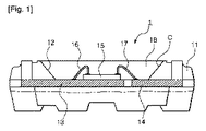
図1は一般的な発光ダイオードパッケージを図示した縦断面図であり、図示したように、従来の発光ダイオードパッケージ1は電源印加時光を発生させる発光源である発光チップ15が中央領域に搭載される。
FIG. 1 is a longitudinal sectional view showing a general light emitting diode package. As shown in the figure, a conventional light
前記発光チップ15は間隔を置いて配置される一対のリードフレーム13、14と金属ワイヤ16、17を媒介にワイヤボンディングされて電気的に連結される。
The
前記陰極及び陽極のリードフレーム13、14は本体の殆どが樹脂物で射出成形されるパッケージ本体11に一体に固定されるが、端部は外部電源と連結されることができるように前記パッケージ本体11の外部面に露出される。
The cathode and
前記パッケージ本体11は射出成形時前記発光チップ15が搭載されて前記金属ワイヤ16、17とワイヤボンディングされるリードフレーム13、14を外部露出させるように上部に開放されたキャビティCを備える。
The
このような前記キャビティCには前記発光チップ15及び金属ワイヤ16、17を外部環境から保護することができるように透光性透明樹脂18を充填するようになり、このような透光性透明樹脂18には具現しようとする発光ダイオードの色によって多様な蛍光体が選択的に含まれることができる。
The cavity C is filled with a translucent
そして、前記キャビティCの内部の傾斜面には前記発光チップ15から発生される光の反射率を高めることができるように反射物質がコーティングされる反射部材12を備えることもできる。
In addition, the inclined surface inside the cavity C may include a
一方、このような発光ダイオードパッケージの特性を決定する基準は、色、輝度及び輝度の強さ範囲などであり、これは主として前記発光チップ15の自体特性によって影響を受けるが、副次的な要素で前記発光チップ15を実装するパッケージ本体11の構造、透光性透明樹脂18の充填量によっても影響を受けるようになる。
On the other hand, the criteria for determining the characteristics of such a light emitting diode package are color, luminance, intensity range of luminance, and the like, which are mainly influenced by the characteristics of the
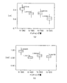
図2は一般的な発光ダイオードパッケージで透光性透明樹脂のドッティング(dotting)量の変化による光輝度の変化を図示したグラフであり、(a)は0.6T発光ダイオードパッケージの場合であり、(b)は0.8T発光ダイオードパッケージの場合である。 FIG. 2 is a graph illustrating a change in light luminance due to a change in the amount of dotting of a transparent transparent resin in a general light emitting diode package. FIG. 2A is a case of a 0.6T light emitting diode package. (B) shows the case of 0.8T light emitting diode package.
図2(a)、(b)に図示したように、前記パッケージ本体11のキャビティCに充填される透光性透明樹脂18のドッティング量が少ないほど光輝度が高くなることが分かる。
As shown in FIGS. 2A and 2B, it can be seen that the light luminance increases as the dotting amount of the translucent
しかし、前記透光性透明樹脂18のドッティング量を減らすと光輝度が高くなるという長所があるが、前記透光性透明樹脂18の高さが低くなり金属ワイヤ16、17が外部に露出されるという問題点があった。
However, if the amount of dotting of the translucent
本発明は上記の問題点を解決するために導き出されたものであり、本発明の目的は、キャビティに充填される透光性透明樹脂の充填使用量を減らすとともに樹脂の充填高さを低くして光輝度を向上させることができて、パッケージの大きさを減らして小型化を図る発光ダイオードパッケージを提供することにある。 The present invention has been derived in order to solve the above-described problems. The object of the present invention is to reduce the amount of translucent transparent resin used in the cavity and to reduce the resin filling height. Accordingly, it is an object of the present invention to provide a light emitting diode package which can improve light brightness and reduce the size of the package to reduce the size.
以上のような目的を達成すべく、本発明は少なくとも一つの発光チップと金属ワイヤを媒介に連結される一対のリードフレーム;前記リードフレームが一体に固定されて、上部に開放されたキャビティを形成するように形成されるパッケージ本体;前記パッケージ本体の外部実装面の下部に下向折曲されて形成されるリードフレーム;前記発光チップを覆いながら前記キャビティに充填される透光性透明樹脂;前記キャビティの底面から下部に陥没形成されて前記発光チップを搭載する陥没部;及び前記陥没部及びキャビティに形成される蛍光体を含む透明樹脂;を含む発光ダイオードパッケージを提供する。 In order to achieve the above object, the present invention provides a pair of lead frames connected via at least one light emitting chip and a metal wire; the lead frames are integrally fixed to form an open cavity at the top. A package body formed to be formed; a lead frame formed by bending downward at a lower portion of an external mounting surface of the package body; a translucent transparent resin that fills the cavity while covering the light emitting chip; There is provided a light emitting diode package including a depressed portion that is recessed from a bottom surface of a cavity to mount the light emitting chip; and a transparent resin that includes a phosphor formed in the depressed portion and the cavity.
また、本発明による発光ダイオードパッケージの前記陥没部の深さは50um〜400umであることができる。 The depth of the depressed portion of the light emitting diode package according to the present invention may be 50 μm to 400 μm.
また、本発明による発光ダイオードパッケージの前記蛍光体はYAG(イットリウム・アルミニウム・ガーネット)系、TAG(テルビウム・アルミニウム・ガーネット)系、シリケート(Silicate)系、スルフィド(Sulfide)系またはナイトライド(NiTride)系のうち少なくとも何れか一つであることができる。 The phosphor of the light emitting diode package according to the present invention may be YAG (yttrium, aluminum, garnet), TAG (terbium, aluminum, garnet), silicate, sulfide, or nitride. It can be at least one of the systems.
また、本発明による発光ダイオードパッケージの前記陥没部は互いに向い合うリードフレームの端部の間に一定の深さで陥没形成される凹溝で備えられることができる。 In addition, the recessed portion of the light emitting diode package according to the present invention may be provided with a recessed groove that is recessed at a certain depth between the end portions of the lead frames facing each other.
また、本発明による発光ダイオードパッケージの前記発光チップの外部面と向い合うリードフレームの端部には前記発光チップの光を反射させる反射部材が備えられる下部傾斜面を備えることができる。 The light emitting diode package according to the present invention may further include a lower inclined surface provided with a reflection member that reflects light of the light emitting chip at an end portion of the lead frame facing the outer surface of the light emitting chip.
また、本発明による発光ダイオードパッケージの前記キャビティは前記発光チップの光を反射させる反射部材が備えられる上部傾斜面を備えることができる。 In addition, the cavity of the light emitting diode package according to the present invention may include an upper inclined surface provided with a reflecting member that reflects light of the light emitting chip.
上記の構成の本発明によると、発光チップの搭載のためにリードフレームまたは互いに向い合うリードフレームの間に陥没部を備えることによって、パッケージ本体の高さを低くしてキャビティ内に充填される透光性透明樹脂の充填使用量を減らして、製造コストを低減し、また光輝度を向上させることができる一方、製品の小型化を図ることができる。 According to the present invention having the above-described configuration, a recessed portion is provided between the lead frames or the lead frames facing each other for mounting the light emitting chip, thereby reducing the height of the package body and filling the cavity. The filling amount of the light transparent resin can be reduced, the manufacturing cost can be reduced, and the light luminance can be improved, while the product can be downsized.
以下では本発明の具体的な実施例を図面を参照して詳細に説明する。但し、本発明の思想は提示される実施例に制限されず、他の構成要素の追加、変更、削除等によって、退歩的な他の発明や本発明の思想の範囲内に含まれる他の実施例を容易に提案することができる。 Hereinafter, specific embodiments of the present invention will be described in detail with reference to the drawings. However, the idea of the present invention is not limited to the embodiments shown, and other implementations included in the scope of the idea of other inventions that are step-by-step or the present invention by adding, changing, or deleting other components. Examples can be proposed easily.
図3は本発明による発光ダイオードパッケージの第1実施例を図示した断面図である。 FIG. 3 is a cross-sectional view illustrating a first embodiment of a light emitting diode package according to the present invention.
本発明の第1実施例によるパッケージ100は発光チップ111、リードフレーム112、113、パッケージ本体115、透光性透明樹脂116及び前記発光チップ111が搭載される陥没部118を備える。
The
前記発光チップ111は電源印加時光を発生させる発光素子で備えられて、このような発光チップ111はP極とN極がチップの上部面に水平型で備えられる。
The
このような発光チップ111は一対の金属ワイヤ114a、114bの各一端部とボンディング接続されて、前記リードフレーム112、113は前記一対の金属ワイヤ114a、114bの各他端部と夫々ボンディング接続される。
The
そして、前記パッケージ本体115は底面が密閉されて上部は開放されたキャビティ117を形成するように樹脂物で射出成形される成形構造物である。
The
ここで、前記キャビティ117は一定角度で傾いた上部傾斜面を備えて、前記上部傾斜面には前記発光チップ111から発生された光を反射させることができるようにAl、Ag、Niのように反射率が高い金属材からなる反射部材117aを備えることもできる。
Here, the
このようなパッケージ本体115は前記一対のリードフレーム112、113が一体に成形されてこれを固定して、前記リードフレーム112、113の一端部の上部面の一部はキャビティ117の底面を介して外部に露出される。
In such a
前記リードフレーム112、113の他端部は外部電源と連結されるように前記パッケージ本体115の外部面に露出される。
The other ends of the
前記陥没部118は一対のリードフレーム112、113のうち前記発光チップ111が搭載されるリードフレーム112に形成されることができる。
The
図4は本発明による発光ダイオードパッケージの第2実施例を図示した断面図である。 FIG. 4 is a cross-sectional view illustrating a second embodiment of the light emitting diode package according to the present invention.
図4を参照すると、第2実施例の発光ダイオードパッケージは第1実施例の前記陥没部118とは異なり、互いに向い合う一対のリードフレーム112、113の端部の間に前記パッケージ本体115の成形時キャビティ117の底面から一定の深さで陥没形成される凹溝118aを備える。それ以外の構成要素は第1実施例と同一である。
Referring to FIG. 4, the light emitting diode package of the second embodiment is different from the
一方、前記透光性透明樹脂116は前記発光チップ111及び金属ワイヤ114a、114bを覆って外部環境から保護するように、前記キャビティ117に充填されるエポキシ、シリコン及びレジン等のような透明な樹脂材からなる。
On the other hand, the translucent
ここで、前記透光性透明樹脂116には前記発光チップから発生された光を白色光に変換させることができるYAG系、TAG系、シリケート系、スルフィド系またはナイトライド系のうち何れか一つの波長変換手段である蛍光物質が含まれることができる。
Here, the translucent
YAG系及びTAG系の蛍光物質には(Y、Tb、Lu、Sc、La、Gd、Sm)3(Al、Ga、In、Si、Fe)5(O、S)12:Ceの中から選択して使用可能であり、シリケート系の蛍光物質には(Sr、Ba、Ca、Mg)2SiO4:(Eu、F、Cl)の中から選択して使用可能である。また、スルフィド系の蛍光物質には(Ca、Sr)S:Eu、(Sr、Ca、Ba)(Al、Ga)2S4:Euの中から選択して使用可能であり、ナイトライド系の蛍光物質には(Sr、Ca、Si、Al、O)N:Eu(例、CaAlSiN4:Eu β-SiAlON:Eu)またはCa-α SiAlON:Eu系である(Cax、My)(Si、Al)12(O、N)16蛍光体成分の中から選択して使用することができる。ここでMはEu、Tb、YbまたはErのうち少なくとも一つの物質であり、xとyは0.05<(x+y)<0.3、0.02<x<0.27and0.03<y<0.3の条件を満たす。 (Y, Tb, Lu, Sc, La, Gd, Sm) 3 (Al, Ga, In, Si, Fe) 5 (O, S) 12 : Ce selected for YAG and TAG fluorescent materials As the silicate fluorescent material, (Sr, Ba, Ca, Mg) 2 SiO 4 : (Eu, F, Cl) can be selected and used. The sulfide-based fluorescent material can be selected from (Ca, Sr) S: Eu, (Sr, Ca, Ba) (Al, Ga) 2 S 4 : Eu, and used in a nitride-based fluorescent material. Fluorescent materials are (Sr, Ca, Si, Al, O) N: Eu (eg, CaAlSiN 4 : Eu β-SiAlON: Eu) or Ca-α SiAlON: Eu system (Cax, My) (Si, Al ) 12 (O, N) 16 phosphor components can be selected and used. Here, M is at least one of Eu, Tb, Yb or Er, and x and y are 0.05 <(x + y) <0.3, 0.02 <x <0.27 and 0.03 <. Satisfy the condition of y <0.3.
前記白色光は青色(B)LEDチップに黄色(Y)蛍光体または緑色(G)及び赤色(R)蛍光体または黄色(Y)、緑色(G)、赤色(R)を含むことができる。黄色、緑色及び赤色蛍光体は、青色LEDチップによって励起されて夫々黄色光、緑色光及び赤色光を発して、この黄色光、緑色光及び赤色光は青色LEDチップから放出された一部の青色光と混色されて白色光を出力する。 The white light may include yellow (Y) phosphor or green (G) and red (R) phosphor or yellow (Y), green (G), and red (R) in a blue (B) LED chip. The yellow, green, and red phosphors are excited by the blue LED chip to emit yellow light, green light, and red light, respectively, and the yellow light, green light, and red light are part of the blue light emitted from the blue LED chip. It is mixed with light and outputs white light.
前記青色LEDチップは通常的に用いられるIII族窒化物系半導体を用いることができる。前記窒化物系半導体の基板はサファイア、スピンネル(MgA1204)、SiC、Si、ZnO、GaAs、GaN基板のうち何れか一つから選択されることができる。 The blue LED chip may be a commonly used group III nitride semiconductor. The nitride-based semiconductor substrate may be selected from any one of sapphire, spinnel (MgA1204), SiC, Si, ZnO, GaAs, and GaN substrates.
前記基板上にバッファー層をさらに含むことができて、前記バッファー層は、窒化物半導体系、カーバイド系のうち何れか一つから選択されることが好ましい。 A buffer layer may be further included on the substrate, and the buffer layer is preferably selected from any one of a nitride semiconductor system and a carbide system.
前記バッファー層上にn型窒化物半導体層が形成されて、前記n型窒化物半導体層はn型GaN系半導体層とn型超格子層を含んで構成されることができる。また、前記n型窒化物半導体層は、アンドープ(undoped)GaN層;n型GaNコンタクト層;n型GaNコンタクト層上のn型GaN層;及び前記n型GaN層上のn型超格子層を含んで構成されることができる。この際、前記n型超格子層は、GaN/InGaN系、AlGaN/GaN系、AlGaN/GaN/InGaN系の多層の繰り返し構造で構成されることができ、前記n型GaN系半導体層上にはn型電極をさらに含んで構成されることができる。そして、前記n型GaN系半導体層の断面にはV-形状の歪曲構造が形成されることもできる。前記V-形状の歪曲構造は、平らな成長面と、傾いた成長面がともに存在する。 An n-type nitride semiconductor layer may be formed on the buffer layer, and the n-type nitride semiconductor layer may include an n-type GaN-based semiconductor layer and an n-type superlattice layer. The n-type nitride semiconductor layer includes an undoped GaN layer; an n-type GaN contact layer; an n-type GaN layer on the n-type GaN contact layer; and an n-type superlattice layer on the n-type GaN layer. Can be configured to include. At this time, the n-type superlattice layer may be formed of a GaN / InGaN-based, AlGaN / GaN-based, or AlGaN / GaN / InGaN-based multilayer repetitive structure, An n-type electrode may be further included. In addition, a V-shaped distorted structure may be formed in the cross section of the n-type GaN-based semiconductor layer. The V-shaped distorted structure has both a flat growth surface and an inclined growth surface.
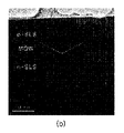
図5は本発明による発光ダイオード層に形成されるV-形状の歪曲構造を示したもので、(a)は平らな成長面と傾いた成長面を図示した断面模式図であり、(b)は傾いた成長面が点線で示された断面実物写真であり、(c)は表面凹凸が形成された平面写真である。 FIG. 5 shows a V-shaped distorted structure formed in a light emitting diode layer according to the present invention. FIG. 5A is a schematic cross-sectional view illustrating a flat growth surface and an inclined growth surface, and FIG. Is a real photograph of a cross section in which a tilted growth surface is indicated by a dotted line, and (c) is a planar photograph in which surface irregularities are formed.
発光チップ111はN型窒化物半導体層で、V-形状の歪曲構造125は平らな成長面127と傾いた成長面129からなる。図5の(b)では傾いた成長面が点線で示されている。
The
前記n型窒化物半導体層上には活性層が形成されて、前記活性層は少なくとも一つ以上の量子井戸層を有し、前記量子井戸層はInGaNまたはGaNで構成されることができて、また前記活性層は少なくとも一つの量子障壁層をさらに含むことができる。前記量子障壁層はInGaN、GaNまたはAlGaNで構成されることができて、量子障壁層のバンドギャップは量子井戸層よりは大きいことが特徴である。 An active layer is formed on the n-type nitride semiconductor layer, the active layer has at least one quantum well layer, and the quantum well layer can be composed of InGaN or GaN. The active layer may further include at least one quantum barrier layer. The quantum barrier layer may be made of InGaN, GaN or AlGaN, and the band gap of the quantum barrier layer is larger than that of the quantum well layer.
前記活性層上にはp型窒化物半導体層が形成されて前記p型窒化物半導体層はp型超格子層とp型GaN系半導体層を含んで構成されて、前記p型超格子層は、GaN/InGaN系、AlGaN/GaN系、AlGaN/GaN/InGaN系の多層の繰り返し構造で構成されることができる。また、前記p型窒化物半導体層は、p型超格子層;前記p型超格子層上のp型GaN層;及び前記p型GaN層上のp型GaNコンタクト層を含んで構成されることができる。 A p-type nitride semiconductor layer is formed on the active layer, and the p-type nitride semiconductor layer includes a p-type superlattice layer and a p-type GaN-based semiconductor layer, and the p-type superlattice layer is GaN / InGaN-based, AlGaN / GaN-based, and AlGaN / GaN / InGaN-based multilayer repetitive structures. The p-type nitride semiconductor layer includes a p-type superlattice layer; a p-type GaN layer on the p-type superlattice layer; and a p-type GaN contact layer on the p-type GaN layer. Can do.
そして、前記p型窒化物半導体層上に透明電極及びボンディング電極をさらに含んで構成される。前記透明電極は透光性の酸化物導電層であることができる。 The p-type nitride semiconductor layer further includes a transparent electrode and a bonding electrode. The transparent electrode may be a translucent oxide conductive layer.
また、前記V-形状の歪曲構造は、前記n型半導体層、活性層、p型半導体層のうち少なくとも何れか一つの層に連続して形成されることができる。前記V-形状の歪曲構造は貫通転位の周りに形成されることができて、この領域の抵抗を高めることによって、前記貫通転位による漏洩電流を防止して、ESD効果を向上させることができる。それだけではなく、前記V-形状の歪曲構造による半導体表面に凹凸構造が形成されてこれによる輝度向上の効果も得ることができる。 The V-shaped distortion structure may be continuously formed on at least one of the n-type semiconductor layer, the active layer, and the p-type semiconductor layer. The V-shaped distorted structure can be formed around threading dislocations, and by increasing the resistance in this region, leakage current due to the threading dislocations can be prevented and the ESD effect can be improved. In addition, a concavo-convex structure is formed on the semiconductor surface by the V-shaped distorted structure, and an effect of improving luminance can be obtained.
即ち、サファイア基板とその上部に形成されるGaN半導体との格子不整合によって貫通転位(threading dislocation)が発生されて、前記貫通転位は静電気が印加される時、電流が集中されて漏洩電流の原因となる。従って、従来には漏洩電流の原因となる貫通転位を減らしてESDによる破損を減らすために多様な研究が行われて来た。即ち、本発明では、前記貫通転位の周りに任意にV-形状の歪曲構造を形成して、前記貫通転位が存在する領域の抵抗を高めることによって、この領域に集中される電流を遮断することで、ESDの耐性を向上させる効果も得ることができる。この際、前記V-形状の歪曲構造層は、600〜900℃の低い成長温度または化学的エッチングと再成長によって形成することができる。このようにして完成された青色LEDチップは基板の厚さを研磨またはエッチング法等で調節して、前記青色LEDチップの全体の厚さを50um〜400umになるように調節することができる。 That is, threading dislocations are generated due to lattice mismatch between the sapphire substrate and the GaN semiconductor formed on the sapphire substrate, and the threading dislocations cause current leakage due to concentration of current when static electricity is applied. It becomes. Therefore, various studies have been conducted in the past in order to reduce threading dislocations that cause leakage currents and reduce ESD damage. That is, in the present invention, an arbitrary V-shaped distorted structure is formed around the threading dislocation to increase the resistance of the region where the threading dislocation exists, thereby blocking the current concentrated in this region. Thus, the effect of improving the ESD resistance can also be obtained. At this time, the V-shaped distorted structure layer can be formed by a low growth temperature of 600 to 900 ° C. or chemical etching and regrowth. The blue LED chip thus completed can be adjusted to have a total thickness of 50 μm to 400 μm by adjusting the thickness of the substrate by polishing or etching.
前記白色光出力のための赤色蛍光体には、N(例、CaAlSiN3:Eu)を含む窒化物(Nitride)系蛍光体を用いることができる。このような窒化物系赤色蛍光体は黄化物(Sulfide)系蛍光体より熱、水分などの外部環境に対する信頼性が優れるだけではなく、変色の恐れが少ない。特に、高色再現性を得るために特定範囲(430〜465nm)に限定した青色LEDチップの主波長で高い蛍光体の励起効率を有する。その他、Ca2Si5N8:Euなどの他の窒化物系蛍光体や黄化物系蛍光体が赤色蛍光体に用いられることもできる。緑色蛍光体には、β-SiAlON:Euの窒化物系または(Bax、Sry、Mgz)SiO4:Eu2+、F、Cl(0<x、y≦2、0≦z≦2、0ppm≦F、Cl≦5000000ppm)のシリケート(Silicate)系蛍光体を用いることができる。このような窒化物系及びシリケート蛍光体も前記青色LEDチップの主波長の範囲(430〜465nm)で高い励起効率を有する。 A nitride phosphor containing N (eg, CaAlSiN 3 : Eu) may be used as the red phosphor for white light output. Such nitride-based red phosphors are not only superior in reliability to the external environment such as heat and moisture but also less likely to be discolored than yellow-based phosphors. In particular, it has a high phosphor excitation efficiency at the main wavelength of a blue LED chip limited to a specific range (430 to 465 nm) in order to obtain high color reproducibility. In addition, other nitride-based phosphors and yellow-based phosphors such as Ca 2 Si 5 N 8 : Eu can be used for the red phosphor. The green phosphor includes β-SiAlON: Eu nitride system or (Ba x , Sr y , Mg z ) SiO 4: Eu 2+ , F, Cl (0 <x, y ≦ 2, 0 ≦ z ≦ 2, A silicate phosphor of 0 ppm ≦ F and Cl ≦ 5000000 ppm can be used. Such nitride-based and silicate phosphors also have high excitation efficiency in the main wavelength range (430-465 nm) of the blue LED chip.
好ましくは、青色LEDチップの半値幅(FWHM)は10〜50nmであり、緑色蛍光体の半値幅は30〜150nmであり、赤色蛍光体の半値幅は50〜200nm程度である。各光源が上記の範囲の半値幅を有することによって、より良い色均一性及び色品質の白色光を得るようになる。特に、青色LEDチップの主波長と半値幅を夫々430〜465nm及び10〜50nmに限定することによって、CaAlSiN3:Eu赤色蛍光体の効率とβ-SiAlON:Eu系または(Bax、Sry、Mgz)SiO4:Eu2+、F、Cl(0<x、y≦2、0≦z≦2、0ppm≦F、Cl≦5000000ppm)系緑色蛍光体の効率を大きく向上させることができる。前記青色LEDチップは主波長の範囲が380〜430nmである紫外線(UV)LEDチップに変えることもできるが、この場合は白色光を出力するためには透光性透明樹脂116に少なくとも青色、緑色、赤色蛍光体が含まれなければならない。青色蛍光体には(Ba、Sr、Ca)5(PO4)3Cl:(Eu2+、Mn2+)またはY2O3:(Bi3+、Eu2+)の中から選択して用いることができて、緑色及び赤色蛍光体は前記YAG系、TAG系、シリケート系、スルフィド系またはナイトライド系の中から選択して用いることができる。
Preferably, the half width (FWHM) of the blue LED chip is 10 to 50 nm, the half width of the green phosphor is 30 to 150 nm, and the half width of the red phosphor is about 50 to 200 nm. When each light source has a half width in the above range, white light with better color uniformity and color quality can be obtained. In particular, by limiting the main wavelength and the half-value width of the blue LED chip to 430 to 465 nm and 10 to 50 nm, respectively, the efficiency of the CaAlSiN 3 : Eu red phosphor and the β-SiAlON: Eu system or (Ba x , Sr y , Mg z ) SiO 4: Eu 2+ , F, Cl (0 <x, y ≦ 2, 0 ≦ z ≦ 2, 0 ppm ≦ F, Cl ≦ 5000000 ppm) can greatly improve the efficiency of the green phosphor. The blue LED chip can be changed to an ultraviolet (UV) LED chip having a main wavelength range of 380 to 430 nm. In this case, at least blue and green are added to the translucent
白色光を出力するための白色LEDは蛍光体を用いなくても作ることができる。例えば、青色光を発する窒化物系のInGaN及び/またはGaNで構成された第1量子井戸層上及び/または下に前記青色光とは異なる波長(例、黄色光)を出す第2量子井戸層をもう一つ形成することによって前記青色光との組合で白色光を発するLEDチップを作ることができる。前記量子井戸層は多重量子井戸構造であることができて、井戸層を形成するInGaNのIn量を調節して第1及び第2量子井戸層を作ることができる。前記第1量子井戸層がUV領域(380〜430nm)の光を発するとしたら、前記第2量子井戸層は青色光を、そして第3量子井戸層は黄色光を発するように活性層のIn量を調節して作ることができる。 A white LED for outputting white light can be produced without using a phosphor. For example, a second quantum well layer that emits a wavelength (for example, yellow light) different from that of the blue light on and / or below the first quantum well layer composed of nitride-based InGaN and / or GaN that emits blue light. Thus, an LED chip that emits white light in combination with the blue light can be produced. The quantum well layer may have a multiple quantum well structure, and the first and second quantum well layers may be formed by adjusting an In amount of InGaN forming the well layer. If the first quantum well layer emits light in the UV region (380 to 430 nm), the amount of In in the active layer is such that the second quantum well layer emits blue light and the third quantum well layer emits yellow light. Can be made by adjusting.
一方、前記陥没部118は前記キャビティ117の底面に露出されるリードフレーム112、113の上部面が下部に一定の深さで陥没形成される。
Meanwhile, the recessed
このような前記陥没部118は、少なくとも一つの発光チップ111が搭載されるリードフレーム112の一端部に下向折曲される折曲部で備えられて、このような折曲部は前記発光チップ111が搭載される平らな搭載面と、前記搭載面から左右両側に一定角度上向に傾くように延長されて前記発光チップ111の外部面と向い合う左右一対の下部傾斜面112a、112aで備えられる。
The
このような下部傾斜面112a、112aには前記発光チップ111の発光時発生された光を反射させることができるように反射部材が備えられることもできる。
The lower inclined surfaces 112a and 112a may be provided with a reflecting member so that the light generated when the
このような陥没部118、118aの形成深さHはこれに搭載される発光チップ111の高さhを考慮して50um〜400umの深さであれば十分である。このようにすることによって、パッケージ本体のキャビティの高さHを150um〜500umに低くすることができて、キャビティ内に充填される透光性透明樹脂の充填使用量を減らして製造コストを低減し、また光輝度を向上させることができる一方、製品の小型化を図ることができる。
The formation depth H of the
そして、前記凹溝118aに搭載された発光チップ111の外部面と向い合うリードフレーム112、113の端部には前記発光チップ111の発光時発生された光を反射させることができるように反射部材が備えられる下部傾斜面112b、113bを夫々備えることが好ましい。
A reflection member may reflect the light generated when the
一方、上述のような構成を有する発光ダイオードパッケージ100、100aはキャビティ117の真中に配置される発光チップ111が前記リードフレーム112に下向折曲形成される折曲部の搭載面に搭載されたり、互いに向い合うリードフレーム112、113の互いに向い合う端部の間に陥没形成される凹溝118aに搭載されることによって、前記リードフレーム112、113と金属ワイヤ114a、114bを媒介にワイヤボンディングされる発光チップ111の上部面は前記リードフレーム112、113の上部面の高さと略同一になるように配置することもできる。
Meanwhile, the light emitting
このような場合、前記発光チップ111とワイヤボンディングされる金属ワイヤ114a、114bの最大の高さは前記発光チップ111の搭載高さが低くなっただけ低くすることができる。
In such a case, the maximum height of the
これによって、前記発光チップ111及び金属ワイヤ114a、114bを保護するように前記キャビティ117に充填される透光性透明樹脂116の充填量を減らすことができる一方、前記透光性樹脂の充填高さHも前記発光チップ111の搭載高さが低くなっただけ低くすることができて、これにより前記発光チップの発光時発生された光の光輝度を従来に比べて相対的に高めることができる。
Accordingly, the filling amount of the transparent
そして、前記キャビティ117に充填される透光性透明樹脂116の充填高さHを低くすることによって前記パッケージ本体115の上端高さも前記充填高さが低くなっただけ低くしてパッケージの全体の大きさをより小型化することができる。
Then, by lowering the filling height H of the translucent
図6の(a)から(c)は本発明による発光ダイオードパッケージで外部のリードフレームを形成する工程を図示した概路図である。 FIGS. 6A to 6C are schematic views illustrating a process of forming an external lead frame in the light emitting diode package according to the present invention.
図6の(a)から(c)を参照すると、まず、陰極及び陽極リードフレーム112、113は本体の殆どが樹脂物で射出成形されるパッケージ本体115に一体に固定されるが、端部は外部電源と連結されるように前記パッケージ本体115の外部面に露出される(図6の(a))。
Referring to FIGS. 6A to 6C, first, the cathode and anode lead frames 112 and 113 are integrally fixed to a package
前記パッケージ本体115の外部に下向露出されたリードフレーム112、113はパッケージの側面及び/または下面を介して折曲されてキャビティ117が形成された発光面とは反対方向に折曲されて形成される。
The lead frames 112 and 113 exposed downward to the outside of the
本発明のパッケージ100では前記パッケージの外部に下向露出されたリードフレーム112、113はパッケージの実装面(底面119)の側面及び/または裏面(後方または下部)にリードフレームが折曲形成されている。
In the
形成過程は、まずパッケージ底面に露出されたリードフレーム112の端部を1次に折曲してパッケージ100の側面の形状に合わせて(図6の(b))、次にパッケージ底面119の後方に折曲して全体リードフレーム112の形状を完成する(図6の(c))。
In the formation process, first, the end portion of the
前記のような構成からなる本発明による発光ダイオードパッケージによって、発光チップの搭載のためにリードフレームまたは互いに向い合うリードフレームの間に陥没部を備えることによって、パッケージ本体の高さを低くしてキャビティ内に充填される透光性透明樹脂の充填使用量を減らして製造コストを低減し、また光輝度を向上させることができる一方、製品の小型化を図ることができるため、産業上の利用可能性が非常に高い。 According to the light emitting diode package according to the present invention having the above-described configuration, the cavity of the package body can be reduced by providing a recessed portion between the lead frame or the lead frames facing each other for mounting the light emitting chip. The amount of translucent transparent resin filled inside can be reduced to reduce the manufacturing cost, and the light brightness can be improved. The nature is very high.
Claims (6)
前記リードフレームが一体に固定されて、上部に開放されたキャビティを形成するように形成されるパッケージ本体;
前記パッケージ本体の外部実装面の下部に下向折曲されて形成されるリードフレーム;
前記発光チップを覆いながら前記キャビティに充填される透光性透明樹脂;
前記キャビティの底面から下部に陥没形成されて前記発光チップを搭載する陥没部;及び
前記陥没部及びキャビティに形成される蛍光体を含む透明樹脂;
を含む発光ダイオードパッケージ。 A pair of lead frames connected via at least one light emitting chip and a metal wire;
A package body formed such that the lead frame is fixed integrally to form an open cavity at the top;
A lead frame formed by bending downward at the bottom of the external mounting surface of the package body;
A translucent transparent resin filled in the cavity while covering the light emitting chip;
A recessed portion that is recessed from the bottom of the cavity to mount the light emitting chip; and a transparent resin that includes a phosphor formed in the recessed portion and the cavity;
Including light emitting diode package.
Applications Claiming Priority (3)
| Application Number | Priority Date | Filing Date | Title |
|---|---|---|---|
| KR20070136265 | 2007-12-24 | ||
| PCT/KR2008/007692 WO2009082177A2 (en) | 2007-12-24 | 2008-12-24 | Light emitting diode package |
| KR1020080133439A KR20090069146A (en) | 2007-12-24 | 2008-12-24 | Light emitting diode package |
Publications (2)
| Publication Number | Publication Date |
|---|---|
| JP2011508416A true JP2011508416A (en) | 2011-03-10 |
| JP2011508416A5 JP2011508416A5 (en) | 2012-01-19 |
Family
ID=40996444
Family Applications (1)
| Application Number | Title | Priority Date | Filing Date |
|---|---|---|---|
| JP2010539313A Pending JP2011508416A (en) | 2007-12-24 | 2008-12-24 | Light emitting diode package |
Country Status (6)
| Country | Link |
|---|---|
| US (1) | US20110049552A1 (en) |
| EP (1) | EP2232595A4 (en) |
| JP (1) | JP2011508416A (en) |
| KR (1) | KR20090069146A (en) |
| CN (1) | CN101939852A (en) |
| WO (1) | WO2009082177A2 (en) |
Families Citing this family (21)
| Publication number | Priority date | Publication date | Assignee | Title |
|---|---|---|---|---|
| US20120168810A1 (en) * | 2009-07-10 | 2012-07-05 | Furukawa Electric Co., Ltd. | Lead frame for optical semiconductor device, method of producing the same, and optical semiconductor device |
| JP5383611B2 (en) * | 2010-01-29 | 2014-01-08 | 株式会社東芝 | LED package |
| JP5799212B2 (en) * | 2010-09-21 | 2015-10-21 | パナソニックIpマネジメント株式会社 | Light emitting module, backlight device and display device |
| MY170920A (en) | 2010-11-02 | 2019-09-17 | Carsem M Sdn Bhd | Leadframe package with recessed cavity for led |
| CN102130278B (en) * | 2010-12-31 | 2013-04-03 | 昆山琉明光电有限公司 | Package of light emitting diode |
| CN103460416B (en) * | 2011-02-10 | 2016-11-09 | 日亚化学工业株式会社 | Light-emitting device, the manufacture method of light-emitting device and array of packages |
| KR20120096216A (en) * | 2011-02-22 | 2012-08-30 | 삼성전자주식회사 | Light emitting device package |
| MY156107A (en) | 2011-11-01 | 2016-01-15 | Carsem M Sdn Bhd | Large panel leadframe |
| US9142745B2 (en) * | 2013-08-27 | 2015-09-22 | Glo Ab | Packaged LED device with castellations |
| TW201517323A (en) | 2013-08-27 | 2015-05-01 | Glo Ab | Molded LED package and method of making same |
| KR20150042362A (en) * | 2013-10-10 | 2015-04-21 | 삼성전자주식회사 | Light emitting diode package and method of manufacturing the same |
| WO2015139190A1 (en) * | 2014-03-18 | 2015-09-24 | 深圳市瑞丰光电子股份有限公司 | Led frame and led illuminant |
| WO2016163595A1 (en) * | 2015-04-08 | 2016-10-13 | 한국광기술원 | Nitride semiconductor light-emitting device, and method for manufacturing same |
| CN106025047A (en) * | 2016-06-30 | 2016-10-12 | 王正作 | LED Package and packaging method thereof |
| CN105914286A (en) * | 2016-06-30 | 2016-08-31 | 王正作 | Multi-tube core LED package and packaging method thereof |
| US11367820B2 (en) | 2017-09-01 | 2022-06-21 | Suzhou Lekin Semiconductor Co., Ltd. | Light emitting device package and light source device |
| CN107958948A (en) * | 2017-12-28 | 2018-04-24 | 广东晶科电子股份有限公司 | A kind of LED light emitting diodes and preparation method thereof |
| US11444227B2 (en) | 2019-10-01 | 2022-09-13 | Dominant Opto Technologies Sdn Bhd | Light emitting diode package with substrate configuration having enhanced structural integrity |
| US11444225B2 (en) | 2020-09-08 | 2022-09-13 | Dominant Opto Technologies Sdn Bhd | Light emitting diode package having a protective coating |
| US11329206B2 (en) | 2020-09-28 | 2022-05-10 | Dominant Opto Technologies Sdn Bhd | Lead frame and housing sub-assembly for use in a light emitting diode package and method for manufacturing the same |
| CN116435201B (en) * | 2023-06-12 | 2023-09-12 | 四川遂宁市利普芯微电子有限公司 | Plastic packaging method and device packaging structure |
Citations (4)
| Publication number | Priority date | Publication date | Assignee | Title |
|---|---|---|---|---|
| JP2004095576A (en) * | 2002-08-29 | 2004-03-25 | Toshiba Corp | Optical semiconductor device and optical semiconductor module, and method for manufacturing optical semiconductor device |
| JP2005294736A (en) * | 2004-04-05 | 2005-10-20 | Stanley Electric Co Ltd | Manufacturing method for semiconductor light emitting device |
| JP2006222271A (en) * | 2005-02-10 | 2006-08-24 | Ngk Spark Plug Co Ltd | Substrate for mounting light-emitting element |
| JP2008053726A (en) * | 2006-08-23 | 2008-03-06 | Seoul Semiconductor Co Ltd | Light emitting diode package |
Family Cites Families (12)
| Publication number | Priority date | Publication date | Assignee | Title |
|---|---|---|---|---|
| TW414924B (en) * | 1998-05-29 | 2000-12-11 | Rohm Co Ltd | Semiconductor device of resin package |
| KR100425566B1 (en) * | 1999-06-23 | 2004-04-01 | 가부시키가이샤 시티즌 덴시 | Light emitting diode |
| WO2001059851A1 (en) * | 2000-02-09 | 2001-08-16 | Nippon Leiz Corporation | Light source |
| JP2002223005A (en) * | 2001-01-26 | 2002-08-09 | Toyoda Gosei Co Ltd | Light emitting diode and display device |
| JP4045781B2 (en) * | 2001-08-28 | 2008-02-13 | 松下電工株式会社 | Light emitting device |
| JP4009097B2 (en) * | 2001-12-07 | 2007-11-14 | 日立電線株式会社 | LIGHT EMITTING DEVICE, ITS MANUFACTURING METHOD, AND LEAD FRAME USED FOR MANUFACTURING LIGHT EMITTING DEVICE |
| JP4359195B2 (en) | 2004-06-11 | 2009-11-04 | 株式会社東芝 | Semiconductor light emitting device, manufacturing method thereof, and semiconductor light emitting unit |
| KR20070000638A (en) * | 2005-06-28 | 2007-01-03 | 삼성전기주식회사 | High brightness light emitting diode and method of manufacturing the same |
| EP1816688B1 (en) * | 2006-02-02 | 2016-11-02 | LG Electronics Inc. | Light emitting diode package |
| JP2007305785A (en) * | 2006-05-11 | 2007-11-22 | Nichia Chem Ind Ltd | Light emitting device |
| US7960819B2 (en) * | 2006-07-13 | 2011-06-14 | Cree, Inc. | Leadframe-based packages for solid state emitting devices |
| EP1928026A1 (en) * | 2006-11-30 | 2008-06-04 | Toshiba Lighting & Technology Corporation | Illumination device with semiconductor light-emitting elements |
-
2008
- 2008-12-24 WO PCT/KR2008/007692 patent/WO2009082177A2/en active Application Filing
- 2008-12-24 EP EP08864310A patent/EP2232595A4/en not_active Withdrawn
- 2008-12-24 JP JP2010539313A patent/JP2011508416A/en active Pending
- 2008-12-24 KR KR1020080133439A patent/KR20090069146A/en not_active Application Discontinuation
- 2008-12-24 CN CN200880122685XA patent/CN101939852A/en active Pending
- 2008-12-24 US US12/810,097 patent/US20110049552A1/en not_active Abandoned
Patent Citations (4)
| Publication number | Priority date | Publication date | Assignee | Title |
|---|---|---|---|---|
| JP2004095576A (en) * | 2002-08-29 | 2004-03-25 | Toshiba Corp | Optical semiconductor device and optical semiconductor module, and method for manufacturing optical semiconductor device |
| JP2005294736A (en) * | 2004-04-05 | 2005-10-20 | Stanley Electric Co Ltd | Manufacturing method for semiconductor light emitting device |
| JP2006222271A (en) * | 2005-02-10 | 2006-08-24 | Ngk Spark Plug Co Ltd | Substrate for mounting light-emitting element |
| JP2008053726A (en) * | 2006-08-23 | 2008-03-06 | Seoul Semiconductor Co Ltd | Light emitting diode package |
Also Published As
| Publication number | Publication date |
|---|---|
| WO2009082177A2 (en) | 2009-07-02 |
| WO2009082177A3 (en) | 2009-08-13 |
| CN101939852A (en) | 2011-01-05 |
| KR20090069146A (en) | 2009-06-29 |
| US20110049552A1 (en) | 2011-03-03 |
| EP2232595A4 (en) | 2011-06-22 |
| EP2232595A2 (en) | 2010-09-29 |
Similar Documents
| Publication | Publication Date | Title |
|---|---|---|
| JP2011508416A (en) | Light emitting diode package | |
| JP6062431B2 (en) | Semiconductor light emitting device | |
| JP4991026B2 (en) | Light emitting device | |
| JP3809760B2 (en) | Light emitting diode | |
| US9172019B2 (en) | Light emitting device package and method of manufacturing the same | |
| JP4411892B2 (en) | Light source device and vehicle headlamp using the same | |
| JP5066786B2 (en) | Nitride phosphor and light emitting device using the same | |
| JP2008243904A (en) | Semiconductor light-emitting element, manufacturing method therefor, and light-emitting device | |
| US20150287876A1 (en) | Light-emitting device | |
| US8053798B2 (en) | Light emitting device | |
| KR20230118056A (en) | Led lighting apparatus having improved color lendering and led filament | |
| US10199540B2 (en) | Light emitting diode, light emitting diode package including same, and lighting system including same | |
| US10385266B2 (en) | Phosphor composition, light emitting element package comprising same, and lighting system | |
| KR20110117415A (en) | Semiconductor light emitting device, package using the same and method of manufacturing thereof | |
| KR20120139127A (en) | Phosphor, phosphor manufacturing method, and light emitting device | |
| JP2016225568A (en) | Nitride semiconductor light-emitting element | |
| KR101659359B1 (en) | Light Emitting Device | |
| US10510925B2 (en) | Light-emitting device and lighting system comprising same | |
| JP6221387B2 (en) | Light emitting device and manufacturing method thereof | |
| KR102579649B1 (en) | Lgiht emitting device | |
| KR102199997B1 (en) | Light emitting device and light emitting device package | |
| JP3674387B2 (en) | Light emitting diode and method for forming the same | |
| KR102628787B1 (en) | Light emitting device | |
| KR100936001B1 (en) | Nitride semiconductor light emitting device and manufacturing method thereof | |
| KR20180051848A (en) | Semiconductor device |
Legal Events
| Date | Code | Title | Description |
|---|---|---|---|
| A521 | Written amendment |
Free format text: JAPANESE INTERMEDIATE CODE: A523 Effective date: 20111121 |
|
| A621 | Written request for application examination |
Free format text: JAPANESE INTERMEDIATE CODE: A621 Effective date: 20111121 |
|
| A711 | Notification of change in applicant |
Free format text: JAPANESE INTERMEDIATE CODE: A712 Effective date: 20120813 |
|
| A131 | Notification of reasons for refusal |
Free format text: JAPANESE INTERMEDIATE CODE: A131 Effective date: 20130129 |
|
| A977 | Report on retrieval |
Free format text: JAPANESE INTERMEDIATE CODE: A971007 Effective date: 20130130 |
|
| RD04 | Notification of resignation of power of attorney |
Free format text: JAPANESE INTERMEDIATE CODE: A7424 Effective date: 20130321 |
|
| A02 | Decision of refusal |
Free format text: JAPANESE INTERMEDIATE CODE: A02 Effective date: 20130625 |