WO2012133760A1 - 電子部品実装方法、電子部品実装システムおよび基板 - Google Patents
電子部品実装方法、電子部品実装システムおよび基板 Download PDFInfo
- Publication number
- WO2012133760A1 WO2012133760A1 PCT/JP2012/058567 JP2012058567W WO2012133760A1 WO 2012133760 A1 WO2012133760 A1 WO 2012133760A1 JP 2012058567 W JP2012058567 W JP 2012058567W WO 2012133760 A1 WO2012133760 A1 WO 2012133760A1
- Authority
- WO
- WIPO (PCT)
- Prior art keywords
- substrate
- layer
- electronic component
- electronic components
- component mounting
- Prior art date
- Legal status (The legal status is an assumption and is not a legal conclusion. Google has not performed a legal analysis and makes no representation as to the accuracy of the status listed.)
- Ceased
Links
Images


Classifications
-
- H—ELECTRICITY
- H10—SEMICONDUCTOR DEVICES; ELECTRIC SOLID-STATE DEVICES NOT OTHERWISE PROVIDED FOR
- H10W—GENERIC PACKAGES, INTERCONNECTIONS, CONNECTORS OR OTHER CONSTRUCTIONAL DETAILS OF DEVICES COVERED BY CLASS H10
- H10W90/00—Package configurations
-
- H—ELECTRICITY
- H10—SEMICONDUCTOR DEVICES; ELECTRIC SOLID-STATE DEVICES NOT OTHERWISE PROVIDED FOR
- H10P—GENERIC PROCESSES OR APPARATUS FOR THE MANUFACTURE OR TREATMENT OF DEVICES COVERED BY CLASS H10
- H10P72/00—Handling or holding of wafers, substrates or devices during manufacture or treatment thereof
- H10P72/04—Apparatus for manufacture or treatment
- H10P72/0446—Apparatus for mounting on conductive members, e.g. leadframes or conductors on insulating substrates
-
- H—ELECTRICITY
- H10—SEMICONDUCTOR DEVICES; ELECTRIC SOLID-STATE DEVICES NOT OTHERWISE PROVIDED FOR
- H10P—GENERIC PROCESSES OR APPARATUS FOR THE MANUFACTURE OR TREATMENT OF DEVICES COVERED BY CLASS H10
- H10P72/00—Handling or holding of wafers, substrates or devices during manufacture or treatment thereof
- H10P72/70—Handling or holding of wafers, substrates or devices during manufacture or treatment thereof for supporting or gripping
- H10P72/74—Handling or holding of wafers, substrates or devices during manufacture or treatment thereof for supporting or gripping using temporarily an auxiliary support
- H10P72/7428—Handling or holding of wafers, substrates or devices during manufacture or treatment thereof for supporting or gripping using temporarily an auxiliary support used to support diced chips prior to mounting
-
- H—ELECTRICITY
- H10—SEMICONDUCTOR DEVICES; ELECTRIC SOLID-STATE DEVICES NOT OTHERWISE PROVIDED FOR
- H10P—GENERIC PROCESSES OR APPARATUS FOR THE MANUFACTURE OR TREATMENT OF DEVICES COVERED BY CLASS H10
- H10P72/00—Handling or holding of wafers, substrates or devices during manufacture or treatment thereof
- H10P72/70—Handling or holding of wafers, substrates or devices during manufacture or treatment thereof for supporting or gripping
- H10P72/74—Handling or holding of wafers, substrates or devices during manufacture or treatment thereof for supporting or gripping using temporarily an auxiliary support
- H10P72/744—Details of chemical or physical process used for separating the auxiliary support from a device or a wafer
-
- H—ELECTRICITY
- H10—SEMICONDUCTOR DEVICES; ELECTRIC SOLID-STATE DEVICES NOT OTHERWISE PROVIDED FOR
- H10W—GENERIC PACKAGES, INTERCONNECTIONS, CONNECTORS OR OTHER CONSTRUCTIONAL DETAILS OF DEVICES COVERED BY CLASS H10
- H10W72/00—Interconnections or connectors in packages
- H10W72/01—Manufacture or treatment
- H10W72/0198—Manufacture or treatment batch processes
-
- H—ELECTRICITY
- H10—SEMICONDUCTOR DEVICES; ELECTRIC SOLID-STATE DEVICES NOT OTHERWISE PROVIDED FOR
- H10W—GENERIC PACKAGES, INTERCONNECTIONS, CONNECTORS OR OTHER CONSTRUCTIONAL DETAILS OF DEVICES COVERED BY CLASS H10
- H10W72/00—Interconnections or connectors in packages
- H10W72/071—Connecting or disconnecting
- H10W72/0711—Apparatus therefor
- H10W72/07141—Means for applying energy, e.g. ovens or lasers
-
- H—ELECTRICITY
- H10—SEMICONDUCTOR DEVICES; ELECTRIC SOLID-STATE DEVICES NOT OTHERWISE PROVIDED FOR
- H10W—GENERIC PACKAGES, INTERCONNECTIONS, CONNECTORS OR OTHER CONSTRUCTIONAL DETAILS OF DEVICES COVERED BY CLASS H10
- H10W72/00—Interconnections or connectors in packages
- H10W72/071—Connecting or disconnecting
- H10W72/0711—Apparatus therefor
- H10W72/07178—Means for aligning
-
- H—ELECTRICITY
- H10—SEMICONDUCTOR DEVICES; ELECTRIC SOLID-STATE DEVICES NOT OTHERWISE PROVIDED FOR
- H10W—GENERIC PACKAGES, INTERCONNECTIONS, CONNECTORS OR OTHER CONSTRUCTIONAL DETAILS OF DEVICES COVERED BY CLASS H10
- H10W72/00—Interconnections or connectors in packages
- H10W72/071—Connecting or disconnecting
- H10W72/072—Connecting or disconnecting of bump connectors
- H10W72/07231—Techniques
- H10W72/07232—Compression bonding, e.g. thermocompression bonding
-
- H—ELECTRICITY
- H10—SEMICONDUCTOR DEVICES; ELECTRIC SOLID-STATE DEVICES NOT OTHERWISE PROVIDED FOR
- H10W—GENERIC PACKAGES, INTERCONNECTIONS, CONNECTORS OR OTHER CONSTRUCTIONAL DETAILS OF DEVICES COVERED BY CLASS H10
- H10W72/00—Interconnections or connectors in packages
- H10W72/071—Connecting or disconnecting
- H10W72/072—Connecting or disconnecting of bump connectors
- H10W72/07231—Techniques
- H10W72/07236—Soldering or alloying
-
- H—ELECTRICITY
- H10—SEMICONDUCTOR DEVICES; ELECTRIC SOLID-STATE DEVICES NOT OTHERWISE PROVIDED FOR
- H10W—GENERIC PACKAGES, INTERCONNECTIONS, CONNECTORS OR OTHER CONSTRUCTIONAL DETAILS OF DEVICES COVERED BY CLASS H10
- H10W72/00—Interconnections or connectors in packages
- H10W72/071—Connecting or disconnecting
- H10W72/073—Connecting or disconnecting of die-attach connectors
-
- H—ELECTRICITY
- H10—SEMICONDUCTOR DEVICES; ELECTRIC SOLID-STATE DEVICES NOT OTHERWISE PROVIDED FOR
- H10W—GENERIC PACKAGES, INTERCONNECTIONS, CONNECTORS OR OTHER CONSTRUCTIONAL DETAILS OF DEVICES COVERED BY CLASS H10
- H10W72/00—Interconnections or connectors in packages
- H10W72/20—Bump connectors, e.g. solder bumps or copper pillars; Dummy bumps; Thermal bumps
- H10W72/241—Dispositions, e.g. layouts
- H10W72/242—Dispositions, e.g. layouts relative to the surface, e.g. recessed, protruding
-
- H—ELECTRICITY
- H10—SEMICONDUCTOR DEVICES; ELECTRIC SOLID-STATE DEVICES NOT OTHERWISE PROVIDED FOR
- H10W—GENERIC PACKAGES, INTERCONNECTIONS, CONNECTORS OR OTHER CONSTRUCTIONAL DETAILS OF DEVICES COVERED BY CLASS H10
- H10W72/00—Interconnections or connectors in packages
- H10W72/20—Bump connectors, e.g. solder bumps or copper pillars; Dummy bumps; Thermal bumps
- H10W72/241—Dispositions, e.g. layouts
- H10W72/244—Dispositions, e.g. layouts relative to underlying supporting features, e.g. bond pads, RDLs or vias
-
- H—ELECTRICITY
- H10—SEMICONDUCTOR DEVICES; ELECTRIC SOLID-STATE DEVICES NOT OTHERWISE PROVIDED FOR
- H10W—GENERIC PACKAGES, INTERCONNECTIONS, CONNECTORS OR OTHER CONSTRUCTIONAL DETAILS OF DEVICES COVERED BY CLASS H10
- H10W72/00—Interconnections or connectors in packages
- H10W72/20—Bump connectors, e.g. solder bumps or copper pillars; Dummy bumps; Thermal bumps
- H10W72/251—Materials
- H10W72/252—Materials comprising solid metals or solid metalloids, e.g. PbSn, Ag or Cu
-
- H—ELECTRICITY
- H10—SEMICONDUCTOR DEVICES; ELECTRIC SOLID-STATE DEVICES NOT OTHERWISE PROVIDED FOR
- H10W—GENERIC PACKAGES, INTERCONNECTIONS, CONNECTORS OR OTHER CONSTRUCTIONAL DETAILS OF DEVICES COVERED BY CLASS H10
- H10W72/00—Interconnections or connectors in packages
- H10W72/20—Bump connectors, e.g. solder bumps or copper pillars; Dummy bumps; Thermal bumps
- H10W72/29—Bond pads specially adapted therefor
-
- H—ELECTRICITY
- H10—SEMICONDUCTOR DEVICES; ELECTRIC SOLID-STATE DEVICES NOT OTHERWISE PROVIDED FOR
- H10W—GENERIC PACKAGES, INTERCONNECTIONS, CONNECTORS OR OTHER CONSTRUCTIONAL DETAILS OF DEVICES COVERED BY CLASS H10
- H10W72/00—Interconnections or connectors in packages
- H10W72/90—Bond pads, in general
- H10W72/941—Dispositions of bond pads
- H10W72/9415—Dispositions of bond pads relative to the surface, e.g. recessed, protruding
-
- H—ELECTRICITY
- H10—SEMICONDUCTOR DEVICES; ELECTRIC SOLID-STATE DEVICES NOT OTHERWISE PROVIDED FOR
- H10W—GENERIC PACKAGES, INTERCONNECTIONS, CONNECTORS OR OTHER CONSTRUCTIONAL DETAILS OF DEVICES COVERED BY CLASS H10
- H10W72/00—Interconnections or connectors in packages
- H10W72/90—Bond pads, in general
- H10W72/951—Materials of bond pads
- H10W72/952—Materials of bond pads comprising metals or metalloids, e.g. PbSn, Ag or Cu
-
- H—ELECTRICITY
- H10—SEMICONDUCTOR DEVICES; ELECTRIC SOLID-STATE DEVICES NOT OTHERWISE PROVIDED FOR
- H10W—GENERIC PACKAGES, INTERCONNECTIONS, CONNECTORS OR OTHER CONSTRUCTIONAL DETAILS OF DEVICES COVERED BY CLASS H10
- H10W74/00—Encapsulations, e.g. protective coatings
- H10W74/10—Encapsulations, e.g. protective coatings characterised by their shape or disposition
- H10W74/15—Encapsulations, e.g. protective coatings characterised by their shape or disposition on active surfaces of flip-chip devices, e.g. underfills
-
- H—ELECTRICITY
- H10—SEMICONDUCTOR DEVICES; ELECTRIC SOLID-STATE DEVICES NOT OTHERWISE PROVIDED FOR
- H10W—GENERIC PACKAGES, INTERCONNECTIONS, CONNECTORS OR OTHER CONSTRUCTIONAL DETAILS OF DEVICES COVERED BY CLASS H10
- H10W80/00—Direct bonding of chips, wafers or substrates
- H10W80/011—Manufacture or treatment of pads or other interconnections to be direct bonded
- H10W80/016—Cleaning
-
- H—ELECTRICITY
- H10—SEMICONDUCTOR DEVICES; ELECTRIC SOLID-STATE DEVICES NOT OTHERWISE PROVIDED FOR
- H10W—GENERIC PACKAGES, INTERCONNECTIONS, CONNECTORS OR OTHER CONSTRUCTIONAL DETAILS OF DEVICES COVERED BY CLASS H10
- H10W80/00—Direct bonding of chips, wafers or substrates
- H10W80/301—Bonding techniques, e.g. hybrid bonding
- H10W80/312—Bonding techniques, e.g. hybrid bonding characterised by the direct bonding of electrically conductive pads
-
- H—ELECTRICITY
- H10—SEMICONDUCTOR DEVICES; ELECTRIC SOLID-STATE DEVICES NOT OTHERWISE PROVIDED FOR
- H10W—GENERIC PACKAGES, INTERCONNECTIONS, CONNECTORS OR OTHER CONSTRUCTIONAL DETAILS OF DEVICES COVERED BY CLASS H10
- H10W80/00—Direct bonding of chips, wafers or substrates
- H10W80/301—Bonding techniques, e.g. hybrid bonding
- H10W80/327—Bonding techniques, e.g. hybrid bonding characterised by the direct bonding of insulating parts, e.g. of silicon oxide layers
-
- H—ELECTRICITY
- H10—SEMICONDUCTOR DEVICES; ELECTRIC SOLID-STATE DEVICES NOT OTHERWISE PROVIDED FOR
- H10W—GENERIC PACKAGES, INTERCONNECTIONS, CONNECTORS OR OTHER CONSTRUCTIONAL DETAILS OF DEVICES COVERED BY CLASS H10
- H10W90/00—Package configurations
- H10W90/20—Configurations of stacked chips
- H10W90/297—Configurations of stacked chips characterised by the through-semiconductor vias [TSVs] in the stacked chips
-
- H—ELECTRICITY
- H10—SEMICONDUCTOR DEVICES; ELECTRIC SOLID-STATE DEVICES NOT OTHERWISE PROVIDED FOR
- H10W—GENERIC PACKAGES, INTERCONNECTIONS, CONNECTORS OR OTHER CONSTRUCTIONAL DETAILS OF DEVICES COVERED BY CLASS H10
- H10W90/00—Package configurations
- H10W90/701—Package configurations characterised by the relative positions of pads or connectors relative to package parts
- H10W90/721—Package configurations characterised by the relative positions of pads or connectors relative to package parts of bump connectors
- H10W90/722—Package configurations characterised by the relative positions of pads or connectors relative to package parts of bump connectors between stacked chips
-
- H—ELECTRICITY
- H10—SEMICONDUCTOR DEVICES; ELECTRIC SOLID-STATE DEVICES NOT OTHERWISE PROVIDED FOR
- H10W—GENERIC PACKAGES, INTERCONNECTIONS, CONNECTORS OR OTHER CONSTRUCTIONAL DETAILS OF DEVICES COVERED BY CLASS H10
- H10W90/00—Package configurations
- H10W90/701—Package configurations characterised by the relative positions of pads or connectors relative to package parts
- H10W90/721—Package configurations characterised by the relative positions of pads or connectors relative to package parts of bump connectors
- H10W90/724—Package configurations characterised by the relative positions of pads or connectors relative to package parts of bump connectors between a chip and a stacked insulating package substrate, interposer or RDL
-
- H—ELECTRICITY
- H10—SEMICONDUCTOR DEVICES; ELECTRIC SOLID-STATE DEVICES NOT OTHERWISE PROVIDED FOR
- H10W—GENERIC PACKAGES, INTERCONNECTIONS, CONNECTORS OR OTHER CONSTRUCTIONAL DETAILS OF DEVICES COVERED BY CLASS H10
- H10W90/00—Package configurations
- H10W90/701—Package configurations characterised by the relative positions of pads or connectors relative to package parts
- H10W90/731—Package configurations characterised by the relative positions of pads or connectors relative to package parts of die-attach connectors
- H10W90/734—Package configurations characterised by the relative positions of pads or connectors relative to package parts of die-attach connectors between a chip and a stacked insulating package substrate, interposer or RDL
-
- H—ELECTRICITY
- H10—SEMICONDUCTOR DEVICES; ELECTRIC SOLID-STATE DEVICES NOT OTHERWISE PROVIDED FOR
- H10W—GENERIC PACKAGES, INTERCONNECTIONS, CONNECTORS OR OTHER CONSTRUCTIONAL DETAILS OF DEVICES COVERED BY CLASS H10
- H10W90/00—Package configurations
- H10W90/701—Package configurations characterised by the relative positions of pads or connectors relative to package parts
- H10W90/791—Package configurations characterised by the relative positions of pads or connectors relative to package parts of direct-bonded pads
- H10W90/792—Package configurations characterised by the relative positions of pads or connectors relative to package parts of direct-bonded pads between multiple chips
Definitions
- the present invention relates to a technique for mounting an electronic component such as a semiconductor chip (hereinafter also simply referred to as a chip) on a substrate.
- a semiconductor chip hereinafter also simply referred to as a chip
- Patent Document 1 the following technique is described. Specifically, first, after applying a non-conductive adhesive (resin layer) on the substrate, a semiconductor chip (hereinafter also simply referred to as a chip) is placed on the substrate and temporarily fixed. Then, the substrate and the chip are heated and pressed to melt the solder bumps (solder bumps provided on the substrate side) provided on the lower surface of the chip. As a result, the chip is bonded onto the substrate.
- a non-conductive adhesive resin layer
- solder bumps solder bumps provided on the substrate side
- an object of the present invention is to provide a mounting technique that can more efficiently realize mounting a plurality of electronic components on a substrate in a planar arrangement.
- a first aspect of the present invention is an electronic component mounting method, and a) an i-th resin on an i-th substrate (where i is an integer of 1 or more) which is a temporary substrate.
- the predetermined substrate and the i-th substrate are relatively brought close to each other in a state where the substrate and the plurality of electronic components of the i-th layer disposed on the i-th substrate are opposed to each other.
- the i-th layer is maintained while the electronic component is bonded to the predetermined substrate.
- And separating the substrate of the first i from a plurality of electronic components is an electronic component mounting method comprising.
- an electronic component mounting system in which an i-th resin layer formed on an i-th substrate (where i is an integer of 1 or more) is a temporary substrate.
- a plurality of electronic components of i layer are placed in a face-up state with their joint surfaces facing upward, and a plurality of electronic components of i layer are arranged in a plane on the i th resin layer and temporarily fixed.
- the predetermined substrate and the i-th substrate are relatively brought close to each other with the bonding means, the predetermined substrate, and the plurality of electronic components of the i-th layer disposed on the i-th substrate facing each other.
- a state in which a plurality of electronic components of the i-th layer are bonded to the predetermined substrate While lifting is an electronic component mounting system comprising a separation means for separating the substrate of the first i from a plurality of electronic components of the i-th layer.
- the present invention is also directed to a substrate used in an electronic component mounting method.
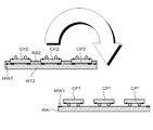
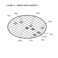
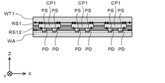
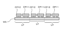
- FIG. 26 illustrates a state where a plurality of chips of three layers are stacked.
- a through electrode VA is provided in each chip (specifically, a silicon (Si) chip) CP (see FIG. 33).
- illustration of the penetration electrode VA is abbreviate
- the present invention is also applicable to the case where the through electrode VA is not provided in each chip CP.
- a plurality of layers of chips are stacked on the substrate WA.
- the stacking operation of each layer is basically the same as each other.
- each chip CP1 of the first layer is “directly” with respect to the substrate WA (a chip other than the chip CP1 is interposed between the chip CP1 and the substrate WA).
- each chip CPi of the i-th layer is bonded to the substrate WA. It is different in that it is bonded to each chip of the (i-1) -th layer laminated (so-called, each chip CPi is “indirectly bonded to the substrate WA”).
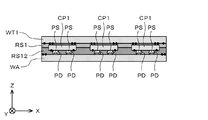
- the substrate WA that is the original mounting target of each chip CPi is used, and a temporary substrate WTi (described later) for temporary placement (temporary fixing) of each chip CPi is also used. Used.
- steps S11 to S14 are executed, whereby the first layer chip stacking operation (see also step S10 and FIG. 2) is performed on the substrate WA.
- a plurality of chips CP1 in the first layer are joined (see also FIGS. 6 to 19).
- the stacking operation of the chips of the second and subsequent layers (i-th layer) (i ⁇ 2) (see also step S20 and FIG. 3) is as follows. (See also FIGS. 20 to 25).
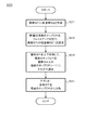
- Step S21 The i-th resin layer RSi is formed on the i-th substrate WTi that is a temporary substrate.
- Step S22 A plurality of chips CPi in the i-th layer are arranged in a plane on the resin layer RSi on the substrate WTi in a face-up state and temporarily fixed.
- Step S23 A plurality of chips CP (i-1) of the (i-1) th layer arranged (directly or indirectly) on the substrate WA and a plurality of i-th layers arranged on the i-th substrate WTi.
- the substrate WA and the i-th substrate WTi relatively approach each other with the chip CPi facing each other, the plurality of chips CP (i-1) of the (i-1) -th layer and the i-th layer
- the plurality of chips CPi are relatively brought close to each other, and the plurality of chips CP (i-1) in the (i-1) th layer and the plurality of chips CPi in the i-th layer are joined (directly).
- the substrate WTi is turned upside down to hold the plurality of i-th layer chips CPi on the substrate WTi in a face-down state.
- the plurality of chips CP (i-1) in the (i-1) layer are relatively brought close to each other, and the plurality of chips CPi in the i-th layer are changed to the plurality of chips CP (i-1) in the (i-1) -th layer.
- the plurality of chips CP (i-1) in the (i-1) -th layer and the plurality of chips CPi in the i-th layer are bonded to each other.
- Step S24 While maintaining the state in which the plurality of chips CPi in the i-th layer are respectively joined to the plurality of chips CP (i-1) in the (i-1) -th layer, from the plurality of chips CPi in the i-th layer The substrate WTi is separated.
- the processing in step S24 is also referred to as debonding processing.
- a plurality of i-th layer chips CPi are stacked and bonded on the (i-1) -th layer chips CP (i-1) bonded onto the substrate WA. .
- the electronic components are laminated in a plurality of layers (multilayer lamination) at a plurality of planar positions on the substrate WA.
- steps S11 to S14 related to the first layer are the same as the corresponding processes in steps S21 to S24 related to the second and subsequent layers.
- steps S13 and S14 are different from the processes in steps S23 and S24, respectively, in the points described above. That is, in steps S23 and S24, the chip CPi of the i-th layer (i ⁇ 2) after the second layer is placed on the chip CP (i-1) of the (i-1) -th layer that has already been stacked. In contrast, in steps S13 and S14, the first layer chip CP1 is directly placed on the substrate WA.
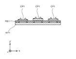
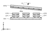
- FIG. 4 is a top view showing a schematic configuration of a chip mounting system (electronic component mounting system) 1.
- a chip mounting system electronic component mounting system
- FIG. 4 and the like directions and the like are shown using an XYZ orthogonal coordinate system for convenience.
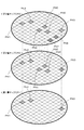
- This chip mounting system 1 is a system for stacking and mounting multilayer chips at a plurality of planar positions of a substrate (substrate to be mounted). For example, the chip mounting system 1 can bond a plurality of chips CP1 in the first layer on the target substrate WA. The chip mounting system 1 can also stack and bond a plurality of second-layer chips CP2 and the like on a plurality of first-layer chips CP1 arranged on the substrate WA.
- the substrate WA is a semiconductor wafer
- each temporary substrate WTi (described later) is a glass substrate.
- the present invention is not limited to this, and each of the substrates WA and WTi may be various substrates.
- the chip mounting system 1 is also referred to as a chip supply device 10, a bonding device 30 (also referred to as a COW (Chip On Wafer) bonding device), and a bonding device 50 (a WOW (Wafer On ⁇ Wafer) bonding device). ), A transport unit 70, and a carry-in / out unit 90.
- the chip mounting system 1 also includes a spin coater 80 (not shown).
- the spin coater 80 is an apparatus for forming a resin layer RSi on the temporary substrate WTi using a spin coating technique.
- the chip supply apparatus 10 is an apparatus that takes out each chip CP from the diced wafer and supplies each chip CP (CPi) to the COW bonding apparatus 30.
- the chip supply device 10 includes a protrusion 11 and a chip transfer device 13 (see FIG. 5).
- the COW bonding apparatus 30 planarly arranges a plurality of chips (electronic components) CPi on the resin layer RSi formed on the temporary substrate WTi with the joint surfaces facing upward (face-up state) (planar arrangement). ) And temporarily fixing a plurality of chips to the resin layer RSi.
- a thermoplastic resin is employed as the resin layer RSi.
- the COW bonding apparatus 30 includes a stage 31, a bonding unit 33, an imaging unit 35, a position recognition unit 36 (not shown), and a rotary chip transfer unit 39.
- the imaging unit 35 acquires a light image related to the marks MC1 and MC2 (described later) as image data.
- the position recognition unit 36 recognizes the position of each chip CP on the temporary substrate WTi based on the image captured by the imaging unit 35. Specifically, the position recognition unit 36 recognizes the position of each chip in the direction parallel to the substrate plane of the temporary substrate WTi (the position of each chip in the plane parallel to the substrate WTi) using the marks MC1 and MC2. To do.
- the bonding unit 33 is a member that places a chip on the substrate WTi, and is also referred to as a chip mounter.
- the bonding part 33 has a head part 33H.
- the head portion 33H can adsorb and hold a chip and is also expressed as a chip holding member (electronic component holding member).
- the head portion 33H is movable in the Z direction by a Z direction drive mechanism.
- the stage 31 is movable in the X direction, the Y direction, and the ⁇ direction by an XY ⁇ direction driving mechanism. Thereby, the relative positional relationship between the bonding portion 33 and the stage 31 can be changed, and as a result, the position of each chip CPi on the temporary substrate WTi can be adjusted.
- the transfer unit 70 uses the transfer robot 71 to transfer the substrate (substrate WA and temporary substrate WTi) among the carry-in / out unit 90, the COW bonding apparatus 30, and the WOW bonding apparatus 50.
- the transfer robot 71 of the transfer unit 70 also performs an operation of turning the substrate (particularly the temporary substrate WTi) upside down.
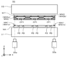
- the WOW bonding apparatus 50 includes a lower stage 51, an upper stage 53, an imaging unit 55 (specifically 55a, 55b), a position recognition unit 56 (not shown), and the like.
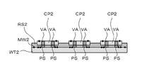
- the imaging unit 55 acquires a light image related to marks MW1 and MW2 (described later) as image data.
- the position recognition unit 56 recognizes the relative positional relationship between the substrate WA held on the lower stage 51 and the temporary substrate WTi held on the upper stage 53 based on the image taken by the imaging unit 55. Specifically, the position recognition unit 56 uses the marks MW1 and MW2 to obtain the relative positional relationship between the substrate WA and the temporary substrate WTi in a direction parallel to the substrate plane of the temporary substrate WTi.
- the upper stage 53 can be moved in the Z direction by a Z direction driving mechanism. Further, the lower stage 51 is movable in the X direction, the Y direction, and the ⁇ direction by the XY ⁇ direction drive mechanism. As a result, the relative positional relationship between the upper stage 53 and the lower stage 51 can be changed. As a result, the positional relationship between the temporary substrate WTi and the substrate WA is adjusted, and further, a plurality of chips in the i-th layer. It is possible to adjust the positional relationship between CPi and the plurality of chips CP (i ⁇ 1) in the (i ⁇ 1) th layer.
- the WOW bonding apparatus 50 is an apparatus that performs a bonding operation between the substrate WA and the temporary substrate WTi. Specifically, the WOW bonding apparatus 50 holds the substrate WA on the lower stage 51 and holds the temporary substrate WTi on the upper stage 53. In the WOW bonding apparatus 50, the substrate WA is arranged with its bonding surface facing upward (face-up state). The temporary substrate WTi is held on the stage 31 in a face-up state in the COW bonding apparatus 30, but the upper stage 53 in a face-down state (with its bonding surface facing downward) in the WOW bonding apparatus 50. Retained.
- the temporary substrate WTi is taken out of the COW bonding apparatus 30 by the transfer robot 71, turned upside down by the transfer robot 71, transferred to the WOW bonding apparatus 50, and held on the upper stage 53 in a face-down state. Is done.
- the WOW bonding apparatus 50 relatively brings the substrates WA and WTi closer together with the substrate WA and the temporary substrate WTi after being turned upside down facing each other. As a result, the plurality of i-th layer chips CPi held in the face-down state on the temporary substrate WTi after being turned upside down approach toward the substrate WA. Then, the plurality of i-th layer chips CPi are bonded to the substrate WA side.
- the WOW bonding apparatus 50 is an apparatus that collectively bonds (bonds) the plurality of chips CPi in the i-th layer and the plurality of chips CP (i-1) in the (i-1) -th layer. It is also called a collective joining device (gang bonder).
- a separation process for separating the temporary substrate WTi from the plurality of chips CPi in the i-th layer is also executed.
- This separation process is performed while maintaining a state in which the plurality of i-th layer chips CPi are bonded to the substrate WA side.
- This separation process is performed by, for example, heating the resin layer RSi of the temporary substrate WTi with a heater (heating processing unit) built in the upper stage 53 that holds the temporary substrate WTi after the ultraviolet irradiation of the resin layer. .
- the WOW bonding apparatus 50 includes a vacuum chamber 59 (not shown) that is a processing space for the substrates WA and WTi (more specifically, the chips CP of each layer) that are objects to be bonded.
- the WOW bonding apparatus 50 includes the above-described lower stage 51, upper stage 53 (see FIG. 17) and the like in a vacuum chamber 59.
- the WOW bonding apparatus 50 can execute chip mounting processing (also expressed as bonding processing related to the substrates WA, WTi, etc.) and the like in the vacuum chamber 59.
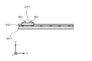
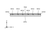
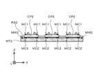
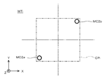
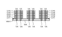
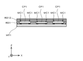
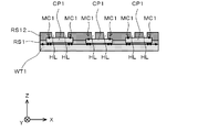
- Chip position adjustment mark MC> As will be described later, in this embodiment (see steps S12 and S22), each chip CP (CPi) is positioned in the horizontal direction on the temporary substrate WTi using alignment marks MC1 and MC2 (see FIG. 8 and the like). Placed.
- Alignment marks MC1 and MC2 are marks for adjusting the position of the chip CP (electronic component), and are also referred to as chip position adjustment marks (or component position adjustment marks).
- chip position adjustment marks or component position adjustment marks.
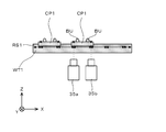
- two marks MC1a and MC1b are provided as the mark MC1 for one chip CP.
- two marks MC2a and MC2b are provided as a mark MC2 per chip CP.
- the two types of marks MC1 and MC2 have different shapes (more specifically, shapes that do not overlap each other). For example, as shown in FIG. 27, a circular mark having a relatively small diameter is used as the mark MC1 (specifically, the marks MC1a and MC1b). On the other hand, as shown in FIG. 28, a circular shape having a relatively large diameter is used as the mark MC2 (specifically, the marks MC2a and MC2b).
- the mark MC1a is provided at the first reference position (planar position) (left front side in FIG. 27) in each chip CP, and the mark MC1b is the second reference position (planar position) in each chip CP (FIG. 27). Then, it is provided on the right back side. Further, the mark MC2a is provided at a regular position (planar position) corresponding to the first reference position of each chip CP on the temporary substrate WTi, and the mark MC2b is the second reference of each chip CP on the temporary substrate WTi. It is provided at a regular position (planar position) corresponding to the position.
- the mark MC2a is provided at a position corresponding to the mark MC1a
- the mark MC2b is provided at a position corresponding to the mark MC1b.
- marks MC1a and MC1b may be provided at positions separated from each other (for example, near both ends of chip CP). preferable. The same applies to the marks MC2a and MC2b.
- the marks MC1a and MC1b are respectively provided on the upper surface (surface opposite to the surface on the temporary substrate WT1 side) of the face-up chip CP1.
- the present invention is not limited to this, and the marks MC1a and MC1b may be provided on the lower surface (surface on the temporary substrate WT1 side) of the chip CP1 in the face-up state, or inside the chip CP1. It may be provided embedded.
- the plurality of temporary substrates WTi have marks MC2 (MC2a, MC2b) corresponding to the chips CPi in the i-th layer at the same reference position (see FIGS. 6 and 20). That is, the plurality of temporary substrates WTi are substrates on which the same plurality of marks MC2 are respectively attached to the same plurality of positions.
- each temporary substrate WTi is physically different from each other, but the present invention is not limited to this, and each temporary substrate WTi may be physically the same substrate. . In other words, one substrate may be used as each temporary substrate WTi.
- Substrate position adjustment mark MW> As will be described later, in this embodiment (see Steps S13 and S23), both the substrates WA and WTi are positioned in the horizontal direction using the alignment marks MW1 and MW2.
- the alignment marks MW1 and MW2 are marks for adjusting the relative positions of the substrates WA and WTi, and are also referred to as substrate position adjustment marks.
- the substrate position adjustment marks MW1 and MW2 have different shapes (more specifically, shapes that do not overlap each other) like the above-described chip position adjustment marks MC1 and MC2.
- a circular shape having a relatively large diameter is used as the mark MW1 (specifically, the marks MW1a and MW1b), and the mark MW2 (specifically, the marks MW2a and MW2b) has a relatively small diameter.
- a circular shape is used.
- the mark MW1a is provided at a first reference position (planar position) in the substrate WA (left end side of the substrate WTi in FIG. 17), and the mark MW1b is a second reference position (planar position) in the substrate WA (in FIG. 17). It is provided on the right end side of the substrate WTi.
- the mark MW2a is provided at a regular position (planar position) corresponding to the first reference position of the substrate WA (the left end side of the substrate WTi in FIG. 17) in the temporary substrate WTi.
- the mark MW2b is provided on the temporary substrate WTi at a regular position (planar position) corresponding to the second reference position on the substrate WA (on the right end side of the substrate WTi in FIG. 17).
- the mark MW2a is provided at a position corresponding to the mark MW1a
- the mark MW2b is provided at a position corresponding to the mark MW1b.
- the marks MW1a and MW1b are preferably provided at positions separated from each other (for example, near both ends of the substrate WA). The same applies to the marks MW2a and MW2b.
- the marks MW1a and MW1b are respectively provided on the upper surface (surface on which each chip is fixed) of the substrate WA in the face-up state.
- the marks MW2a and MW2b are provided on the lower surface of the temporary substrate WTi in the face-down state (the surface on which each chip is temporarily fixed).
- each mark (MC1a, MC1b), (MW1a, MW1b) may be provided on the opposite side surface, or may be provided embedded in each substrate WA, WTi. May be.
- the plurality of temporary substrates WTi have the marks MW2 (MW2a, MW2b) at the same reference position. That is, the plurality of temporary substrates WTi are the same substrates also in the sense that the same mark MW2 is attached at the same position.
- chip mounting operation electroactive component mounting operation
- the present invention is not limited to this, and it may be laminated in two layers, or may be laminated in four or more layers. Alternatively, only one chip layer may be provided on the substrate WA.
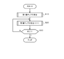
- step S10 First layer chip stacking process
- step S10 the stacking operation of the first layer chips (step S10) (see FIGS. 1 and 2) is performed as follows.
- Step S11 Preparation Step> Specifically, first, in step S11 (FIG. 2), the resin layer RS1 is formed on the substrate WT1 (FIG. 6) which is a temporary substrate (FIG. 7). Note that marks MC2 and MW2 are preliminarily attached to the temporary substrate WT1 before the resin layer RS1 is formed. This resin layer RSi transmits light (infrared light or the like).
- thermoplastic resin thermoplastic adhesive or the like
- the resin layer RS1 is formed on the substrate WT1.
- the resin layer can be formed very easily.
- the present invention is not limited to this, and the resin layer RS1 may be formed on the substrate WT1 by pasting a resin sheet on the substrate WT1. Also by this, a resin layer can be formed very easily.
- the temporary substrate WT1 on which the resin layer RS1 is formed is transferred to the COW bonding apparatus 30 by the transfer robot 71.
- the temporary substrate WT1 is placed on the stage 31 in the COW bonding apparatus 30 and held on the stage 31 (see FIGS. 4 and 5).
- step S12 the plurality of chips CP1 in the first layer are arranged in a plane on the resin layer RS1 in a face-up state and temporarily fixed (see FIGS. 8 to 12 and the like).
- the “face-up state” of each chip CP is a state in which the bonding surface of each chip CP (for example, the surface to which the solder bumps BU are attached) faces upward.
- dicing processing is performed in the chip supply device 10 (FIG. 5) to generate a plurality of chips CP.
- a substrate WC having a plurality of electronic circuits is cut into chips in the vertical and horizontal directions.
- each cut-out chip CP is pushed up one by one by the protruding portion 11 (FIG. 5) of the chip supply device 10 and delivered to the chip transfer device 13 at the position PG1.
- the chip transfer device 13 adsorbs the chip CP at its tip (lower end), moves further upward, and then moves toward the chip transport unit 39 side of the COW bonding device 30.
- the chip transport unit 39 When the chip transport unit 39 receives the chip CP from the chip transfer device 13 at the position PG3, the chip transport unit 39 transports the chip CP to a position PG5 immediately below the head unit 33H of the bonding unit 33 by a rotation operation around the central axis AX.
- the head portion 33H is slightly lowered to the vicinity of the placement position PG5 of the chip CP, receives the chip CP from the chip transport portion 39, and sucks the chip CP at the tip portion (lower end portion) of the head portion 33H. Thereafter, in order to avoid interference with the head unit 33H, the chip transport unit 39 rotates by a predetermined angle, and the head unit 33H descends in a state where the head unit 33H and the chip transport unit 39 do not interfere with each other, and is sucked and held by the head unit 33H. The chip CP is lowered to the position PG7. As a result, the chip CP adsorbed at the tip of the head portion 33H is placed at a predetermined plane position on the temporary substrate WT1 on the stage 31.
- the chip CP (CP1) is positioned and placed on the temporary substrate WT1 as described below.
- the COW bonding apparatus 30 includes a position recognition unit (also referred to as a position measurement unit) 36 as described above.
- the position recognition unit 36 is a processing unit that recognizes the relative position (specifically, X, Y, ⁇ ) between the chip CP and the substrate WTi in the horizontal direction.
- the positioning operation (alignment operation) between each chip CP and the temporary substrate WTi is performed by the position recognition unit 36 in two sets of marks (MC1a, MC2a), (MC1b, MC2b) attached to each chip CP and the temporary substrate WTi. ) Is executed by recognizing the position.
- the position recognizing unit 36 has light sources (emitted light) of the imaging units 35a and 35b having a coaxial illumination system in a state where each chip CP (CP1) held by the head unit 33H faces the temporary substrate WT1.
- the position of the chip CP on the substrate WT1 is recognized using image data relating to the reflected light of illumination light (here, infrared light) emitted from the substrate WT1.
- the light emitted from the light source of the imaging unit 35a passes through the hollow portion of the stage 31, the glass temporary substrate WTi, the resin layer RSi, the silicon (Si) portion of the chip, and the like.
- the light is reflected by the marks MC1a and MC2a, and the reflected light is received by the imaging element of the imaging unit 35a.
- an image including an optical image (optical image by infrared light (reflected light) of each mark portion) regarding each chip and the substrate WTi is acquired as image data Ga. That is, a captured image Ga obtained by simultaneously reading the two types of marks MC1a and MC2a is acquired.
- the position recognizing unit 36 recognizes the position of a certain set of marks (MC1a, MC2a) attached to each chip and the substrate WTi based on the captured image Ga, and also detects the position of the set of marks MC1a, MC2a. The amount of positional deviation ( ⁇ xa, ⁇ ya) between each other is obtained (see FIG. 29).
- the light emitted from the light source of the imaging unit 35b passes through the hollow portion of the stage 31, the glass temporary substrate WTi, the resin layer RSi, the silicon (Si) portion of the chip, and the like.
- the light is reflected by the marks MC1b and MC2b, and the reflected light is received by the imaging device of the imaging unit 35b.
- an image including an optical image (optical image by infrared light (reflected light) of each mark portion) regarding each chip and the substrate WTi is acquired as the image data Gb. That is, a captured image Gb obtained by simultaneously reading the two types of marks MC1b and MC2b is acquired.
- the position recognition unit 36 recognizes the position of a certain set of marks (MC1b, MC2b) attached to each chip and the substrate WTi based on the photographed image Gb, and also detects the position of the set of marks MC1ba, MC2b. A positional shift amount ( ⁇ xb, ⁇ yb) between them is obtained.
- the imaging units 35a and 35b are movable in the X direction, the Y direction, and the Z direction, respectively, and can be adjusted by changing the imaging range.
- the position recognizing unit 36 temporarily sets each chip CP in the horizontal direction (X direction, Y direction, and ⁇ direction) based on the positional deviation amounts ( ⁇ xa, ⁇ ya), ( ⁇ xb, ⁇ yb) of these two sets of marks.
- a relative positional deviation amount ( ⁇ x, ⁇ y, ⁇ ) with respect to the substrate WTi is calculated.
- the stage 31 is appropriately driven in two translational directions (X direction and Y direction) and a rotational direction ( ⁇ direction) so that the relative shift amount recognized by the position recognition unit 36 is reduced. .
- the temporary substrate WTi and the chip CP are relatively moved, and the above-described positional deviation amount is corrected.
- the alignment operation of the chip CP1 (with respect to the X direction, the Y direction, and the ⁇ direction) is executed.
- the head portion 33H holding one chip CP1 of the first layer is further lowered, and the chip CP1 is placed at a predetermined horizontal position of the resin layer RS of the temporary substrate WT1 (see FIG. 9).
- the position recognition operation (position displacement measurement operation) and the alignment driving operation (position displacement correction operation) as described above are performed at least once even after the chip CP is pressed against the resin layer RS and placed. It is preferable to execute again. According to this, a more accurate alignment operation is executed.
- the mounting operation of the second and subsequent chips in the first layer is performed in the same manner (FIGS. 10 and 11).
- the plurality of chips CP1 in the first layer are positioned and arranged at predetermined plane positions on the temporary substrate WTi.
- each of the plurality of chips CP1 in the first layer is positioned in a direction (X, Y, ⁇ ) parallel to the substrate plane (main plane) of the temporary substrate WT1.
- each of the plurality of chips CP1 in the first layer is placed on the resin layer RS1 on the temporary substrate WT1.
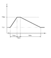
- thermoplastic resin when a thermoplastic resin is used as the resin layer RS, for example, the thermoplastic resin is heated to a temperature T2 (for example, 150 ° C.) lower than a temperature T1 (for example, 200 ° C.) at which the resin layer RS is completely fluidized. Then, each chip is placed in a state where the resin is softened (semi-cured).
- the temperature T2 is preferably lower than the melting point of the solder so that the solder bumps of each chip do not melt.
- the resin layer RS1 is cured by cooling (including heating interruption). Thereby, each chip is temporarily fixed to the resin layer RS1.
- step S12 it is preferable to execute a process (leveling process) for aligning the heights of the plurality of chips in the vertical direction.
- Step S13 WOW process> Thereafter, the process of step S13 is executed.
- step S13 first, the substrate WT1 is held by the transfer robot 71.
- the transfer robot 71 turns the substrate WT1 upside down and transfers the substrate WT1 to the WOW bonding apparatus 50 (see FIG. 16).
- the substrate WT1 after being turned upside down is held on the upper stage 53 of the WOW bonding apparatus 50 (see FIG. 17).
- the plurality of chips CP1 temporarily fixed to the substrate WT1 are held in a face-down state.
- the substrate WA transported by the transport robot 71 is held in advance on the lower stage 51 of the WOW bonding apparatus 50.
- both the substrates WA and WT1 are held with their bonding surfaces facing each other.
- both the substrates WA and WT1 are positioned as described below.
- the WOW bonding apparatus 50 includes the position recognition unit (also referred to as a position measurement unit) 56 as described above.
- the position recognition unit 56 is a processing unit that recognizes the relative position (specifically, X, Y, ⁇ ) between the substrate WA and the substrate WTi in the horizontal direction.
- the positioning operation (alignment operation) between the substrate WA and the temporary substrate WTi (here, WT1) is performed by the position recognition unit 56 with two sets of marks (MW1a, MW2a), ( It is executed by recognizing the position of MW1b, MW2b).
- the position recognition unit 56 includes the imaging units 55a and 55b having a coaxial illumination system in a state where the substrate WA held by the lower stage 51 and the substrate WT1 held by the upper stage 53 face each other.
- the positions of the substrates WA and WTi are recognized using image data relating to the reflected light of illumination light (here, infrared light) emitted from a light source (also referred to as an emission unit).
- the position recognizing unit 56 recognizes the position of a certain set of marks (MW1a, MW2a) attached to both the substrates WA, WTi based on the captured image Gc, and the pair of marks MW1a, MW2a. The amount of misalignment ( ⁇ xc, ⁇ yc) is obtained.
- the position recognizing unit 56 recognizes the position of a certain set of marks (MW1b, MW2b) attached to both the substrates WA, WTi based on the captured image Gd, and reciprocally connects the one set of marks MW1b, MW2b. A positional deviation amount ( ⁇ xd, ⁇ yd) is obtained.
- the imaging units 55a and 55b can move in the X direction, the Y direction, and the Z direction, respectively, and can be adjusted by changing the imaging range.
- the position recognizing unit 56 uses the substrate WA and the temporary substrate in the horizontal direction (X direction, Y direction, and ⁇ direction) based on the positional deviation amounts ( ⁇ xc, ⁇ yc), ( ⁇ xd, ⁇ yd) of these two sets of marks. A relative positional deviation amount ( ⁇ x, ⁇ y, ⁇ ) with respect to WTi is calculated.
- the lower stage 51 is appropriately driven in two translational directions (X direction and Y direction) and a rotational direction ( ⁇ direction) so that the relative shift amount recognized by the position recognition unit 56 is reduced.
- X direction and Y direction translational directions
- ⁇ direction rotational direction
- the alignment operations of the substrates WA and WTi (related to the X direction, the Y direction, and the ⁇ direction) are executed.
- the upper stage 53 is further lowered, the substrate WA and the substrate WTi relatively approach each other, and the plurality of chips CPi (here CP1) held in the face-down state on the temporary substrate WTi and the substrate WA are relatively To approach.
- the plurality of chips CPi in the face-down state are respectively placed at predetermined horizontal positions on the substrate WA (see FIG. 18).
- the “face-down state” of the chip CPi is a state in which the bonding surface of the temporary substrate WTi on which each chip CPi is temporarily fixed (for example, the surface on which the chip CPi is temporarily fixed) faces downward. It is also expressed that the temporary substrate WTi is in a face-down state.
- a process is performed to apply a predetermined pressure between the chip CPi and the substrate WA. It is preferable.
- the substrate WA is heated by the heater built in the lower stage 51 and the substrate WTi is heated by the heater built in the upper stage 53.
- the solder bump BU of each chip CP1 is melted, and a plurality of chips CPi are bonded onto the substrate WA.
- the chip CPi is accurately positioned on the substrate WTi using the marks MC1 and MC2 (step S12), and the substrate WA and the substrate WTi are accurately positioned using the marks MW1 and MW2. Positioning has been performed (step S13). Therefore, the plurality of chips CPi in the face-down state are accurately positioned and bonded to predetermined horizontal positions of the substrate WA.
- each chip CP1 in the first layer is placed at a predetermined position on the substrate WA, and the substrate WA and the plurality of chips CP1 in the first layer are joined (directly).
- step S14 the “debonding process” is executed. Specifically, the substrate WT1 is separated from the plurality of chips CP1 while maintaining the state where the plurality of chips CP1 are respectively mounted (bonded) at predetermined positions on the substrate WA.
- the resin layer RS1 is heated to a predetermined temperature T4 by a heater built in the upper stage 53. Then, in such a heating state, by raising the upper stage 53 while holding the temporary substrate WT1, the temporary substrate WT1 having the resin layer RS1 is peeled from the plurality of chips CP1 (see FIG. 19).
- FIG. 19 schematically shows the temporary substrate WT1 being peeled from the chip CP1.
- the temperature T4 is not high enough to completely fluidize the resin layer RS1, but a temperature at which the resin layer RS1 is semi-cured (for example, 180 ° C.). It is preferable that In order to prevent the solder bump of each chip CP1 bonded to the substrate WA from being melted again, the temperature T4 is preferably lower than the melting point of the solder.
- the plurality of first-layer chips CP1 are bonded to predetermined positions on the substrate WA in a state of being planarly arranged on the substrate WA (step S10).
- step S20 the second layer chip stacking operation (step S20) (see FIGS. 1 and 3) is performed as follows.
- the corresponding processing in steps S21 to S24 related to the second layer is the same as the processing in steps S11 to S14 related to the first layer.
- the chip CPi in the i-th layer is placed on the chip CP (i-1) in the (i-1) -th layer.
- a resin layer RS2 is formed on a substrate WT2 that is a temporary substrate (see FIG. 20). Specifically, resin layer RS2 is formed on temporary substrate WT2 using spin coater 80 or the like. The temporary substrate WT2 on which the resin layer RS2 is formed is placed on the stage 31 in the COW bonding apparatus 30 by the transfer robot 71 and held on the stage 31 (see FIGS. 4 and 5).
- the plurality of chips CP2 in the second layer are arranged in a plane on the resin layer RS2 on the substrate WT2 in a face-up state and temporarily fixed (see FIG. 21).
- each chip CPi (here CP2) cut out from the substrate WC by the chip supply device 10 (FIG. 5) is supplied to the COW bonding device 30 by the protruding portion 11 of the chip supply device 10, the chip transfer device 13, and the like. Is transferred to the chip transfer section 39.
- the chip transport unit 39 transports the chip CP received at the position PG3 to a position PG5 directly below the head unit 33H of the bonding unit 33.
- the head unit 33H is lowered, and the chip CP attracted and held by the head unit 33H is lowered from the position PG5 to the position PG7.
- the chip CP adsorbed at the tip of the head portion 33H is placed at a predetermined plane position on the temporary substrate WT1 on the stage 31.
- each chip CP (CP2) is positioned and placed on the temporary substrate WT2 using the alignment marks MC1 and MC2 provided for each chip CP. Also in step S22, it is preferable to execute a process (leveling process) for aligning the heights of the plurality of chips in the Z direction (vertical direction).
- step S23 first, the temporary substrate WT2 is held by the transfer robot 71.
- the transfer robot 71 turns the temporary substrate WT2 upside down and transfers the temporary substrate WT2 to the WOW bonding apparatus 50 (see FIG. 22).
- the temporary substrate WT2 after being turned upside down is held on the upper stage 53 of the WOW bonding apparatus 50 (see FIG. 23).
- the plurality of chips CP2 temporarily fixed to the temporary substrate WT2 are held in a face-down state.
- the lower stage 51 of the WOW bonding apparatus 50 holds the substrate WA that has been subjected to the process of step S10.
- step S23 in the same manner as in step S13, the relative positions in the horizontal direction of both the substrates WA and WT2 are adjusted using the alignment marks MW1 and MW2 with the temporary substrate WT2 and the substrate WA facing each other.
- the upper stage 53 is further lowered to bring the temporary substrate WT2 and the substrate WA facing each other relatively close to each other, whereby the plurality of chips CP2 and the substrate WA in the second layer in the face-down state (specifically, the substrate WA)
- the plurality of chips CP1) in the first first layer are made relatively close to each other (see FIG. 23).
- a plurality of i-th layer chips CPi (CP2) in the face-down state are arranged at predetermined positions on the substrate WA (specifically, the (i-1) -th layer chip CPi (CP1) already stacked on the substrate WA). (See FIG. 24).
- the substrate WA and the temporary substrate WT2 are positioned in the horizontal direction using the substrate position adjustment mark MW1 on the substrate WA and the substrate position adjustment mark MW2 on the temporary substrate WT2.
- the positional relationship between each of the plurality of first layer chips CP1 held on the substrate WA and each of the plurality of second layer chips CP2 held on the substrate WT2 is adjusted, and each chip CP1 is adjusted. And the corresponding chips CP2 are respectively joined.
- each chip CP2 of the second layer is accurately positioned on the substrate WT2 using the marks MC1 and MC2 (step S22), and the substrate WA and the substrate WT2 are accurately positioned using the marks MW1 and MW2. (Step S23). Therefore, each chip CP2 of the second layer in the face-down state is accurately positioned and bonded to a predetermined horizontal position on the substrate WA (specifically, on each chip CP1 of the first layer of the substrate WA).
- step S24 while maintaining the state in which the plurality of chips CP2 of the second layer are respectively bonded to the substrate WA (specifically, the plurality of chips CP1 of the first layer placed on the substrate WA),
- the substrate WT2 is separated from the plurality of chips CP2 in the second layer. More specifically, the temporary substrate WT2 having the resin layer RS2 is peeled from the plurality of chips CP2 by raising the upper stage 53 while holding the temporary substrate WT2 while the resin layer RS2 is heated to the temperature T4. (See FIG. 25).
- FIG. 25 schematically shows the temporary substrate WT2 being peeled from the chip CP2.
- a plurality of chips CP2 in the second layer are further laminated and bonded on the plurality of chips CP1 in the first layer bonded on the substrate WA.
- step S30 (FIG. 1) If it is determined in step S30 (FIG. 1) that the processing has not yet been completed, the process returns to step S20 again. Then, in the same manner as the second layer stacking operation, the third layer and subsequent chip stacking operations are executed. If it is determined that the final layer chip stacking operation has been completed (YES in step S30), this process ends.
- the stacking operation of the third-layer chip CP3 is performed as follows.
- step S21 the resin layer RS3 is formed on the temporary substrate WT3, and in step S22, the plurality of chips CP3 of the third layer are temporarily fixed in a planar arrangement on the resin layer RS3 in a face-up state.
- step S23 the temporary substrate WT3 is turned upside down, and the plurality of chips CP3 in the third layer are held in the temporary substrate WT3 in a face-down state, and the substrate WA and the temporary substrate WT3 facing each other are relatively close to each other.
- the plurality of chips CP3 in the third layer in the face-down state and the plurality of chips CP2 in the second layer on the substrate WA relatively approach each other, and the plurality of chips CP2 in the second layer and the third layer
- the plurality of chips CP3 are joined to each other.
- step S24 the temporary substrate WT3 is separated from the plurality of chips CP3 in the third layer while maintaining the state in which the plurality of chips CP3 in the third layer are respectively joined to the plurality of chips CP2 in the second layer.
- the plurality of chips CP3 in the third layer are further stacked on the plurality of chips CP1 in the first layer and the plurality of chips CP2 in the second layer stacked on the substrate WA.
- a substrate wafer
- a resin layer is formed on the substrate
- a plurality of chips are planarly placed on the resin layer.
- the chip is temporarily fixed to the resin layer.
- the substrate and the plurality of chips are collectively heated and pressed from above and below, and the solder bumps provided on the lower surface of each chip (specifically, the solder bumps provided on the substrate side) are melted to form a plurality of chips.
- the resin layer on the substrate is formed, for example, by applying a resin material to the substrate by a spin coating technique. Or the said resin layer may be formed by sticking a resin sheet on a board
- this mounting technology is a technology for mounting a single-layer chip layer in which a plurality of chips are arranged in a plane on a substrate (wafer).
- a resin layer may be formed on the first-layer chip when the second-layer chip is stacked on the first-layer chip. Desired.
- a plurality of i-th chips CPi are arranged in a plane in a face-up state on a resin layer RSi formed on a temporary substrate WTi different from the substrate WA. Fixed. Then, the temporary substrate WTi is turned upside down, and the plurality of chips CPi in the i-th layer are held facing the temporary substrate WTi in a face-down state.
- the temporary substrate WTi and the substrate WA on which the chip CP (i-1) of the (i-1) th layer is arranged in plane are relatively approached, and the plurality of chips CPi of the ith layer and the (i -1) The chip CP (i-1) in the layer is bonded to each other. Thereafter, the temporary substrate WTi is separated from the plurality of chips CPi in the i-th layer.
- the plurality of chips CPi in the i-th layer can be easily stacked on the plurality of chips CP (i-1) in the (i-1) -th layer. That is, it is possible to more easily realize that a plurality of chips are stacked and mounted on the substrate.
- the temporary substrate WTi corresponding to each of the component position adjustment mark MC1 in each of the i-th chip CPi and each of the i-th chip CPi is positioned in a direction parallel to the substrate plane of the temporary substrate WTi and mounted on the resin layer RSi on the temporary substrate WTi. Placed. At this time, only the alignment of each chip CPi of one layer (i-th layer) has to be performed on the temporary substrate WTi. In other words, alignment of multiple layers of chips on the temporary substrate WTi is not necessary. Accordingly, it is possible to easily perform an accurate positioning operation of each chip CPi on the temporary substrate WTi.
- a technique also referred to as a technique according to a comparative example
- alignment is performed in a state where a plurality of chips are stacked on the substrate WA.
- a plurality of chips CP of different layers can place the same mark MC1 (MC1a, MC1b) on the same reference position ( Even in the case of (position in the horizontal direction), it is not necessary to align the chips of the plurality of layers on the substrate WA using the mark MC1 of the chips of the plurality of layers.
- the alignment of the chips CPi of one layer (i-th layer) may be performed on the temporary substrate WTi different from the substrate WA. Therefore, each chip can be positioned accurately and easily.
- the temporary substrate WTi is turned upside down, and in steps S13 and S23, the substrate WA and the temporary substrate WTi are formed using the substrate position adjustment mark MW1 on the substrate WA and the substrate position adjustment mark MW2 on the temporary substrate WTi.
- the positional relationship between the substrate WA and the temporary substrate WTi is adjusted by positioning in the direction parallel to the substrate plane of the temporary substrate WTi. According to this, each of the plurality of chips CP1 of the first layer can be accurately positioned and placed at a predetermined position on the substrate WA. Similarly, each chip CPi of the i-th layer held on the temporary substrate WTi is accurately positioned with respect to the corresponding chip CP (i-1) of the (i-1) -th layer held on the substrate WA. Can be placed.
- the plurality of chips CPi in the i-th layer are collectively bonded to the corresponding chips CP (i-1) in the (i-1) -th layer. Therefore, an efficient stacking operation is realized.
- the bonding time can be shortened as compared with the case where a plurality of chips CPi in the i-th layer are bonded to the corresponding chip CP (i-1) in the (i-1) -th layer. Further, by shortening the heating time on the substrate WA, it is possible to suppress the oxidation of the solder on the substrate WA.
- the solder bonding in step S13 (, S23) is performed in a state where the solder bumps BU are not immersed in the resin. Therefore, it is possible to realize highly reliable bonding as compared with the case where the solder bump is immersed in the resin (particularly, when the soldering is performed by adding an activator such as flux to the resin).
- Atmosphere (nitrogen, Ar gas, etc.) formation treatment, reducing atmosphere (hydrogen gas, formic acid gas, etc.) formation treatment, surface activation treatment (detailed later), etc. are possible, and where more reliable bonding is highly productive It becomes possible.
- the COW bonding apparatus 30 it takes 5000 seconds to mount 5000 chips with a mounting time of 1 s (seconds) per chip, and in the WOW bonding apparatus 50, vacuuming is performed over a little over 1 hour. Etc. are performed to perform batch joining. Therefore, the processing time in the COW bonding apparatus 30 and the processing time in the WOW bonding apparatus 50 are close to each other (ideally the same), and good in both processes (between the COW process and the WOW process). Balance (ie, good line balance) can be achieved. That is, bonding with higher reliability is possible at a high productivity with a balanced line.
- the steps of S12 and S22 in the COW bonding apparatus 30 are temporarily fixed (temporarily fixed) to the temporary substrate at a high speed, and after the thousands are mounted, the processes of steps S13 and S23 in the WOW bonding apparatus 50 are performed in a nitrogen atmosphere.
- step S23 solder bonding operation and the like in step S23 will be described in more detail, but the same applies to step S13.
- step S23 when each substrate WTi is transferred into the vacuum chamber 59 (not shown), the internal space of the vacuum chamber 59 is depressurized to be in a vacuum state, and then the nitrogen space is placed in the internal space of the vacuum chamber 59. Is supplied. It should be noted that an appropriate period (for example, about 1 hour) is required from the start of pressure reduction in the internal space of the vacuum chamber 59 to the completion of nitrogen filling. Thereafter, as described above, the positioning operation and the bonding operation regarding both the substrates WA and WTi are executed. Note that the positioning operation may be performed before decompression, not after decompression.
- the solder bumps BU of the plurality of chips CPi and the electrode parts of the plurality of chips CP (i-1) is performed (see FIGS. 23 and 24).
- the thickness of electronic components has also become smaller (thinner). This is because, when a through electrode is provided on a chip or the like by a chip stacking technique, the diameter of the through electrode is further miniaturized, and the production of a “shallow hole” having a miniaturized diameter is miniaturized. This is due to the fact that it is relatively easy to make a “deep hole” of a different diameter.
- the conventional method (specifically, the method of heating and soldering a chip placed on a wafer (also referred to as C4 method (reflow method)) is applied to a relatively thin chip as it is.
- C4 method reflow method
- each chip is heated in the furnace without being pressurized in the vertical direction (see FIG. 72).
- FIG. 72 is a diagram showing a heating state of the chip in such a conventional method.
- a substrate having a single-layer chip disposed on the surface thereof is heated in a heating furnace, and solder bonding between the chip and the substrate is performed.
- the thin chip (CP) is warped by heating.
- this technique is a technique for performing pressure heating and cooling (cooling in a pressurized state) for each predetermined number (for example, five) of chips stacked in the vertical direction according to the number of stacked chips. .
- step S23 an assembly of chips integrated in units of substrates instead of in units of chips (chip units) is joined together, so that an increase in time can be suppressed.
- the processing increase time is about 1 hour as a whole.
- solder bonding is performed in the atmosphere.
- flux is used to prevent solder oxidation.
- the thickness of the plurality of chips CPi (for example, the plurality of chips CP1) in the i-th layer.
- a plurality of chips CP1 are obtained as shown in FIG.
- the upper end position of each chip CP1 (the variation in the upper end position) between the chips CP1.
- the variation in the upper end position appears as variation in the lower end position of the chip CP1 disposed on the upper side when the temporary substrate WT1 is turned upside down and opposed to the substrate WA in step S13 (, S23). Then, if each chip CP1 is pressed toward the substrate WA as it is, a certain chip CP1 is in contact with the substrate WA, while another chip CP1 is not in contact with the substrate WA and may float from the substrate WA. is there.
- a leveling step of aligning the heights of the upper end positions of the plurality of i-th chips CPi temporarily placed on the resin layer RS in the face-up state is provided. Is preferred. According to this, it is possible to absorb the thickness variation of the plurality of chips CPi.
- steps S12 and S22 parallel to the substrate WTi, on the upper end side of the plurality of chips of the i-th layer temporarily placed face-up on the resin layer RS on the substrate WTi.
- the resin layer RS is preferably heated to a temperature T2 that realizes a semi-cured state.
- the resin layer RS is cooled and solidified, whereby each chip CPi is placed in a predetermined position (predetermined horizontal). (Direction position and predetermined vertical position).
- predetermined position predetermined horizontal
- process which aligns the vertical position (Z direction position) of the upper end side of a some chip
- the leveling process may be performed for each chip in step S12.
- the head portion 33H (see FIG. 5) holding each chip CPi of the i-th layer in a face-up state is lowered, and each chip CPi is placed on the resin layer RSi.
- the position of the head portion 33H in the Z direction is adjusted so that the tip of the head portion 33H is lowered to the predetermined position Z0.
- This position Z0 is also expressed as the upper end position (Z direction position) of each chip CPi.
- the position Z0 is a common (identical) position among the plurality of chips CPi.
- each chip CPi in the face-up state is placed on the resin layer RSi with its lower surface (surface opposite to the upper bonding surface) side buried in the resin layer RSi.
- the resin layer RSi has a thickness that can absorb variations in chip thickness (for example, several tens of micrometers to several hundreds of micrometers or more).
- the resin layer RSi is formed of a thermoplastic resin and has a semi-cured state when the chip is placed. For example, the head portion 33H is heated to a predetermined temperature, and the resin layer RSi may be softened by heating the resin layer RSi to the temperature T2 via each chip CPi.
- the semi-cured resin layer RSi is cooled and solidified.
- the chips CPi are temporarily fixed to the resin layer RSi in a state where the heights of the upper end positions of the plurality of chips CPi in the i-th layer are aligned with each other.
- the leveling process as described above may be performed in the COW bonding apparatus 30 or may be performed in the WOW bonding apparatus 50.
- such a leveling process is also useful when the flatness of the stage is impaired along with the heating process (particularly when the leveling process is performed by the WOW bonding apparatus 50 or the like).
- the leveling process as described above in a situation where the center portion of the stage (specifically, the upper stage 53 or the lower stage 51) protrudes by a minute amount from the peripheral portion in accordance with the heat treatment, the surface of the stage Even in the lowered flatness state, the upper end positions of the plurality of chips CPi placed on the surface can be aligned.
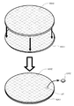
- the planar member PL is pressed against the plurality of chips CPi as shown in FIG.
- the planar member PL is not limited to the one having a completely flat surface, but a very slightly curved surface (for example, A convex curved surface or a concave curved surface).
- the upper end positions of the plurality of chips CPi may be aligned by pressing the planar member having a very slightly curved surface against the plurality of chips CPi.
- the size of the gap between the joining portions facing each other can be made uniform with respect to the plurality of joining portions (arranged in the horizontal direction).
- the planar member PL may be an object to be bonded (other objects to be bonded).
- the variation in chips is about several ⁇ m
- the variation (flatness) due to thermal expansion at about 250 ° C. of the 8-inch wafer size stage is on the order of several tens of ⁇ m.
- the swell of the stage appears as a pressure difference and does not often lead to poor bonding, but in the case of joining in the liquid phase such as solder joining, the flatness of the stage is joined as it is.
- the bumps may be crushed at a portion where the height is reduced, and a short circuit may occur between adjacent bumps. Therefore, it has been difficult to perform solder bonding at the wafer level with the conventional method.
- leveling is performed in a state where the solder is in a solid phase at a temperature near the solder melting point, so that it is possible to perform solder melt bonding by absorbing the swell of the stage even at the solder bonding temperature.
- the leveling process is preferably performed by the WOW bonding apparatus 50, but the leveling process may be performed using another apparatus (such as a dedicated leveling apparatus) having a similar thermal expansion state (similar to the thermal expansion state of the WOW bonding apparatus 50). May be performed.
- Resin layer RS is formed with photocurable resin (ultraviolet curable resin etc.). You may do it.
- each chip is formed by curing or semi-curing the resin by light irradiation (such as ultraviolet irradiation). What is necessary is just to temporarily fix to temporary board
- each chip may be separated from the temporary substrate WTi by using a laser ablation technique as will be described later.
- the leveling process may be performed for each chip in steps S12 and S22 as follows.
- the resin layer RSi has not yet been irradiated with light (ultraviolet rays) and the resin layer RSi has a semi-cured state at the time immediately before the chip placement.
- the head portion 33H holding each chip CPi in the i-th layer in a face-up state moves down and places each chip CPi on the resin layer RSi.
- the position of the head portion 33H in the Z direction is adjusted so that the tip of the head portion 33H is lowered to the predetermined position Z0.
- this position (the upper end position of each chip CPi) Z0 is a common (identical) position among the plurality of chips CPi.
- the mounting region (partial region) RG of the resin layer RSi is cured by irradiating light (ultraviolet rays) to the mounting region RG of the chip CPi immediately after mounting in the semi-cured resin layer RSi. Is done. As a result, the chip CPi is temporarily fixed to the resin layer RSi.
- the same operation is repeatedly executed for a plurality of chips CPi. Specifically, each time the upper end positions of the plurality of chips CPi are aligned and placed on the resin layer RSi, light (ultraviolet rays) is focused on the placement area of each chip in the semi-cured resin layer RSi. The placement region (partial region) of the resin layer RSi is cured by partial irradiation. Thus, the chips CPi are temporarily fixed to the resin layer RSi in a state where the heights of the upper end positions of the i-th layer chips CPi are aligned with each other.
- the resin layer RS may be formed of a thermosetting resin.
- each chip is temporarily fixed to the temporary substrate WTi by heating and curing the uncured resin. Good.
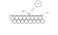
- each chip may be separated from the temporary substrate WTi by using a laser ablation technique (a technique for generating bubbles in the resin layer by irradiating a laser beam).
- the adhesive strength adheresive strength of thermosetting resin as an adhesive
- the leveling process may be performed for each chip as follows. Specifically, first, the upper end position of each chip is arranged at a predetermined position Z0 in the vertical direction. Thereafter, the tip of the head portion 33H is heated to a predetermined temperature, and the resin layer RSi is heated via each chip to cure the resin layer RSi, and each chip may be temporarily fixed to the resin layer RSi. .
- step S24 the technique of heating and melting the resin layer RS to the temperature T4 and peeling the temporary substrate WTi from the chip CP is exemplified, but the present invention is not limited thereto. .
- the internal structure of the resin layer RS is changed by irradiating the resin layer RS formed of a thermoplastic resin with ultraviolet rays, and then the temperature T5 (for example, about 160 ° C.) (lower than the above-described temperature T4)
- the temporary substrate WTi may be peeled off from the chip CP by low-temperature heating with (temperature) (T5 ⁇ T4).
- the ultraviolet rays may be irradiated to the resin layer through the temporary substrate (glass substrate) WTi formed of glass.
- step S11 the temporary substrate WTi is coated with a thermoplastic adhesive, pre-baked at about 180 ° C., and the solvent component is volatilized to form the temporary substrate WTi on the temporary substrate WTi.
- a cured resin layer RSi is formed.
- step S12 the head portion 33H and / or the stage 31 is heated at a low temperature, and a plurality of chips CPi of the i-th layer are placed on the resin layer RSi whose surface is adhesive. Further, the resin layer RSi is heated at a temperature T12 (for example, 200 ° C.) for about 10 minutes to transition the resin layer RSi to a semi-cured state, and then a leveling process is performed using the planar member PL. Thereafter, the resin layer RSi is cooled to temporarily fix each chip CPi to the temporary substrate WTi.
- T12 for example, 200 ° C.
- each chip CPi is preferably provided with solder bumps by high-temperature solder (for example, melting point 280 ° C.).
- the resin is denatured by a heating reaction at 200 ° C. for 10 minutes, and it can withstand without heating even at 300 ° C. during soldering.
- step S13 the upper stage 53 and / or the lower stage 51 of the WOW bonding apparatus 50 are heated to melt the solder bumps of the chips CPi, and the chips CPi of the i-th layer are transferred to the substrate WA. (Or to each chip CP (i-1) of the (i-1) th layer).
- step S14 after the resin layer RSi is heated to a relatively low temperature T5, ultraviolet rays are transmitted through the temporary substrate (glass substrate) WTi and irradiated to the resin layer RSi.
- the internal structure of the resin layer RSi is changed by ultraviolet irradiation, and the resin layer RSi is easily peeled from each chip CPi by, for example, low-temperature heating of about 160 ° C.
- the debonding process as described above may be performed.
- the resin layer RS is formed of an ultraviolet curable resin (UV curable resin)
- a technique that generates bubbles in the resin layer by irradiating the resin layer cured by ultraviolet irradiation with laser light.
- the temporary substrate WTi may be peeled off from the chip CP by an ablation technique.
- the laser beam may be irradiated to the resin layer through the temporary substrate (glass substrate) WTi formed of glass, similarly to the ultraviolet rays.
- a plurality of layers stacked in the vertical direction are heated by heating only the member holding the chip (upper stage 53) without heating the member holding the substrate WA (lower stage 51).
- the temperature rise of the chip CP (i-1) in the relatively lower layer may be suppressed. This prevents re-melting of the solder bumps of the relatively lower chips CP (i-1) that are already bonded. As a result, it is possible to more surely prevent the once-completed bonding of the chips of each layer from being removed by heating when bonding the chips of the upper layer.
- solder having a relatively low melting point may be used as the solder of the chip CPi of the relatively upper layer.
- a solder bump having a melting point lower than that of the solder bump of the first layer chip CP1 may be used as the solder bump of the second layer chip CP2. According to this, remelting or the like of the solder bumps of the chips CP (i-1) that are already bonded relatively lower layers is prevented.
- a solder material whose melting temperature rises at the time of reheating after being once heated and melted and alloyed (as compared with heating before alloying) may be used.
- step S21 is performed as it is after step S14 is illustrated, it is not limited to this.
- an underfill process is provided between step S14 related to the first layer and step S21 related to the second layer (or between step S24 related to the i-th layer and step S21 related to the next (i + 1) -th layer). You may do it. That is, you may make it provide an underfill process after a debonding process.
- a non-conductive resin (NCP: Non-conductive-Paste) is used as the underfill resin RU by a dispenser between the substrate WA and the lower surface of the chip CP1 (or the upper surface of the lower chip CP (i-1)). And a lower surface of the upper chip CPi) (see FIG. 30).
- the filled underfill resin RU is cured by heating or the like. According to this, it is possible to more reliably prevent the once-completed joining of the chips of each layer from being removed by heating at the time of joining the chips of the upper layer.
- a residue cleaning step may be added between step S14 and step S21 (when the above underfill step is provided, etc., before the underfill step).
- the cleaning step is also effective, for example, for cleaning residues that may occur when using a flux together during solder bonding and resin residues after debonding.
- a light-transmitting glass substrate that transmits visible light is used as the temporary substrate WTi, and each mark MC1 (MC1a, MC1b) is placed on each chip CPi in the face-up state. It is provided on the surface FT on the temporary substrate WTi side. Then, an image obtained by simultaneously capturing optical images of the marks MC1 and MC2 obtained through the glass substrate WTi and the light-transmitting resin layer RSi that transmits visible light is acquired as a position recognition image. That's fine.
- each chip CP is provided with a through electrode (for example, made of copper (Cu)) VA, and a solder bump BU is provided on the surface of the through electrode VA.
- a through electrode for example, made of copper (Cu)
- solder bump BU is provided on the surface of the through electrode VA.
- FIG. 33 A case is assumed (see FIG. 33).
- the solder bumps BU are provided only on the upper surface of the through electrode VA is illustrated, but the present invention is not limited to this, and the solder bumps BU are also provided on the lower surface of the through electrode VA (that is, on both upper and lower sides). You may do it.
- the solder bump BU may be provided only on the lower surface of the through electrode VA.
- step S23 nitrogen is supplied into the vacuum chamber 59 after the internal space of the vacuum chamber 59 is depressurized and brought into a vacuum state.
- both the substrates WA and WTi are held in a state in which their joint surfaces face each other, and a positioning operation or the like is performed.
- Chip CPi (specifically, its solder bumps BU)
- Chip CP (i-1) (specifically, its electrode portion (through electrode VA)) is relatively close to the chip CP (i-1), and then is contacted and pressurized to start a bonding operation (solder bonding operation) ( (See FIG. 34).
- the bonding operation is executed with management of the temperature profile during solder bonding (see FIG. 35). Specifically, first, each substrate or the like is heated using a heater on the upper stage 53 side and / or a heater on the lower stage 51 side, and the temperature is set to the temperature TE1 (for example, room temperature) in the temperature increase period TMa (for example, 20 minutes). To a predetermined temperature TE2 (for example, 280 ° C.). Then, after the constant temperature period TMb (for example, 10 minutes) has elapsed, the temperature is lowered from the temperature TE2 to the temperature TE1 in the temperature decrease period TMc (for example, 40 minutes).
- TMa room temperature
- TMb for example, 10 minutes
- step S23 the bonding of the plurality of i-th chips CPi to the substrate WA is performed with the solder bonding process (specifically, the plurality of (i ⁇ 1) -th layers of the substrate WA).
- the solder bonding process using solder provided on at least one bonding surface of the chip CP (i-1) and the plurality of chips i in the i-th layer is performed), and the solder bonding process is performed with a predetermined temperature profile. Executed. In such a temperature profile, a corresponding time (here, a total of 70 minutes) is required.
- step S23 was mainly demonstrated here, it is the same also about step S13.
- the COW bonding apparatus 30 in the COW process by the COW bonding apparatus 30, it takes 5000 seconds to load 5000 chips with a mounting time of 1 s (seconds) per chip.
- the temperature profile temperature increase process, temperature decrease process, etc.
- the processing time in the COW bonding apparatus 30 and the processing time in the WOW bonding apparatus 50 are close to each other (ideally the same), and good in both processes (between the COW process and the WOW process).
- Balance that is, good line balance
- solder bonding is performed in a nitrogen atmosphere, but the present invention is not limited to this.
- solder bonding or the like may be performed in another non-oxidizing atmosphere such as an argon (Ar) gas atmosphere.
- the solder bonding operation may be performed by performing only evacuation without supplying nitrogen (that is, in vacuum).
- the solder bonding operation may be performed in a reducing atmosphere.
- the WOW bonding apparatus 50 evacuates the vacuum chamber 59, then supplies hydrogen gas (and / or formic acid gas, etc.) to the vacuum chamber 59 to form a reducing atmosphere, and solders in the reducing atmosphere. You may make it perform joining operation
- solder bump BU is directly provided on the through electrode VA, but the present invention is not limited to this.
- a solder bump BU may be provided on a copper post (copper pillar) formed on the through electrode VA.
- solder bonding is exemplified, but the present invention is not limited to this, and the present invention can be applied to other bonding.
- the present invention can also be applied to a case where electrode materials (for example, copper (Cu)) are directly bonded (direct bonding) without using solder (solder bump).
- electrode materials for example, copper (Cu)
- solder bump solder bump
- a case is illustrated in which each chip CP is provided with a through electrode (for example, made of copper (Cu)) VA, and a copper (Cu) post PS is further provided on the surface of the through electrode VA. (See FIG. 36).
- the surface activation treatment is performed on the bonding surface (bonding surface) of the electrode material. It is preferable to bond materials (solid phase bonding). In other words, it is preferable to perform a surface activation process on the electrode material provided on the bonding surface when bonding the plurality of i-th chips CPi to the substrate WA. Below, such a modified example is demonstrated.
- solder bump solder bump
- a surface activation process is performed. According to this, it is also possible to realize interlayer bonding by directly bonding copper posts without using bumps. That is, it is possible to perform interlayer bonding by direct bonding of electrodes. Solder bumps and copper posts are collectively referred to as protruding electrodes.
- the WOW bonding apparatus 50 is placed on the bonding surface of each chip (electronic component) placed on the substrate WA and the temporary substrate WTi in a chamber under reduced pressure (vacuum chamber). It is possible to activate each bonding surface of each chip (electronic component) with an atomic beam or the like and bond both bonding surfaces to each other. With such a configuration, it is possible to perform surface activation treatment on both bonding surfaces and perform solid-phase bonding on both the bonded surfaces.
- the WOW bonding apparatus 50 further includes a beam irradiation unit BM (not shown).
- a beam irradiation unit BM (not shown).
- step S13 and S23 the following operation is performed using the beam irradiation unit BM and the like.
- step S23 will be mainly described, but the same applies to step S13.
- step S23 after the substrate WTi is loaded, a vacuum state is formed in the internal space of the vacuum chamber 59 of the WOW bonding apparatus 50.
- the surface of the electrode material of each chip is irradiated with an atomic beam of a specific substance (here, argon (Ar)) using a beam irradiation unit BM or the like, and an argon bombardment process (surface activation process) is executed.
- a specific substance here, argon (Ar)
- BM beam irradiation unit
- argon bombardment process surface activation process
- the beam irradiation unit BM accelerates an ionized specific substance (such as argon) by an electric field toward a bonding surface of an object to be bonded (such as copper (Cu) that is an electrode material).
- a bonding surface of an object to be bonded such as copper (Cu) that is an electrode material.
- the bonding surface of the object to be bonded is activated.
- the beam irradiation unit BM performs a surface activation process that activates the bonding surface of the object to be bonded by irradiating (releasing) energy waves.
- the adhering substance 99 on the bonding surface is removed by causing a specific substance (such as argon) to collide with the bonding surface of the object to be bonded (here, the bonding surface of Cu).
- a dangling bond (indicated by a short line segment in FIG. 43) which is an unbonded hand of the surface atom of the object to be bonded is exposed.
- the bonding surface of an electrode material here, Cu
- a surface activation process is performed by irradiating a bonding surface of VA (here, made of copper) with an atomic beam of a specific substance (here, argon (Ar)).
- heat treatment is also performed with both substrates WA and WTi being pressurized.
- a heat treatment for raising the temperature to about 150 ° C. is performed. Note that this heat treatment also requires a corresponding time (for example, 30 minutes).
- step S23 at least one (here, both) bonding surfaces of the plurality of chips CP (i-1) in the (i-1) th layer and the plurality of chips CPi in the ith layer are provided.
- the surface activation treatment is performed on the electrode material (specifically, the bonding surface thereof).
- the substrate WA in a state where the plurality of chips CP (i-1) in the (i-1) th layer disposed on the substrate WA and the plurality of chips CPi in the ith layer disposed on the substrate WTi are opposed to each other.
- the substrate TWi approaches relatively.
- the plurality of chips CP (i-1) in the (i-1) th layer and the plurality of chips CPi in the ith layer are relatively close to each other, so that the plurality of chips CP (i-1) in the (i-1) th layer. -1) and the plurality of chips CPi in the i-th layer are bonded to each other.
- the joining process involving such surface activation treatment it is possible to obtain a very good joint.
- bonding at a relatively low temperature can be realized. More specifically, bonding is possible at room temperature (25 ° C) to 150 ° C in a vacuum, and bonding at a relatively low temperature of 200 ° C to 250 ° C is possible in a nitrogen atmosphere. It is. In the case where the surface activation treatment is not involved, it is necessary to heat to a relatively high temperature (for example, about 400 ° C. for bonding between copper and about 300 ° C. for bonding between solders).
- the surface activation treatment since bonding at a relatively low temperature can be realized, it is possible to suppress the thermal expansion and realize high-precision bonding. Furthermore, when bonding between different materials is performed, the difference in thermal expansion caused by the difference in thermal expansion coefficient between both materials (dissimilar materials) is realized by realizing bonding at a relatively low temperature. It is also possible to suppress it.
- the present invention is not limited to this, and the surface activation process may be performed in a nitrogen atmosphere.
- the heating step after bonding it is preferable to raise the temperature to about 200 ° C. to 250 ° C. and heat it.
- the copper post PS is provided only on the upper surface of the through electrode VA is illustrated, but the present invention is not limited to this, and the copper post PS is also provided on the lower surface of the through electrode VA (that is, both upper and lower sides). May be provided (see FIG. 38). In such a case, by repeating the above-described processing, it is possible to obtain a multilayer chip as shown in FIG. 41 (five-layer chip in FIG. 41).
- the copper post PS may be provided only on the lower surface of the through electrode VA (see FIG. 37).
- the through electrodes VA may be directly joined without providing the copper post PS (see FIG. 39).
- the surface activation treatment is performed not only on the electrode portion (through electrode VA) but also on the silicon (Si) portion before bonding. According to this, not only the electrode parts but also the silicon parts can be bonded well.
- a multilayer chip five-layer chip in FIG. 42
- a multilayer chip is produced in which not only the electrode parts of adjacent chip layers adjacent in the vertical direction but also the silicon (Si) parts of the adjacent chip layers are well bonded.
- the bonding strength between adjacent chips can be improved.
- a beam irradiation process is illustrated as the surface activation process
- an atomic beam irradiation process is illustrated as the beam irradiation process.
- the present invention is not limited to this.
- ion beam irradiation processing or the like may be employed as the beam irradiation processing.
- ionized specific substances such as argon
- they are immediately combined with the charges supplied in the beam irradiation unit, and the electrical characteristics thereof are neutralized.
- the specific substance electrically neutralized goes to a to-be-joined object at high speed.
- an ionized specific substance such as argon
- an ionized specific substance is released in an ionized state after being accelerated by an electric field. And the said specific substance heads to a to-be-joined object with an ion state.
- argon or the like in an ionic state is electrically neutralized by being combined with electric charges before reaching the surface of the object to be bonded.
- timing of electrical neutralization differs between an ion beam and an atom beam, they are common in that an ionized specific substance (such as argon) is accelerated by an electric field. And it is common also in the point that the surface activation process as shown in FIG. 43 is performed when the accelerated specific substance collides with a joining surface at high speed.
- an ionized specific substance such as argon
- argon is mainly exemplified as the specific substance, but it is not limited to this.
- other inert gases such as krypton (Kr) or xenon (Xe)
- Kr krypton
- Xe xenon
- the through electrode VA is also provided on the substrate WA.
- the through electrode VA of each chip on the substrate WT1 and the corresponding through electrode VA on the substrate WA are also joined together with a surface activation process in the same manner as described above.
- the substrate WA may be provided with electrodes (pads or the like) that are not through electrodes (see FIG. 55).
- the through electrode VA of each chip on the substrate WT1 and the corresponding electrode (pad or the like) on the substrate WA are also joined together with the surface activation process in the same manner as described above.
- the present invention is not limited to this.
- the present invention may be applied when the copper post PS is provided on at least one of the upper surface and the lower surface of the through electrode VA.
- the WOW bonding apparatus 50 is placed on the bonding surface of each chip (electronic component) placed on the substrate WA and the temporary substrate WTi in a chamber under reduced pressure (vacuum chamber). Plasma treatment is performed on the bonding surface of each chip (electronic component) to activate each bonding surface and bond both bonding surfaces to each other.
- the WOW bonding apparatus 50 further includes a plasma processing unit PM (not shown) and the like. Then, in the bonding process (steps S13 and S23), the following operation is executed using the plasma processing unit PM and the like.
- step S23 will be mainly described, but the same applies to step S13.
- step S23 after the substrate WTi is loaded, a vacuum state is formed in the internal space of the vacuum chamber 59 of the WOW bonding apparatus 50.
- oxygen plasma is applied to the surface of each chip (both the exposed surface portion of the through electrode and the silicon portion) using the plasma processing unit PM and the like, and hydrophilic treatment (surface activation treatment) is performed.
- hydrophilic treatment surface activation treatment
- OH groups are generated by exposure to an environment containing moisture. It is also possible to generate OH groups with moisture contained in the atmosphere simply by exposure under a low vacuum after the plasma treatment.
- oxygen plasma processing is illustrated, but other plasma processing (for example, nitrogen plasma processing) may be performed.
- the heat treatment is performed in a state where both the substrates WA and WTi are pressurized. For example, a heat treatment for raising the temperature to about 150 ° C. is performed. Note that this heat treatment requires an appropriate time (for example, 1 hour).
- surface activation treatment by plasma is a chemical reaction treatment of the surface layer of the bonding surface of the object to be bonded by active ions or the like in the plasma to activate the bonding surface of the object to be bonded. It includes a process for facilitating the joining of objects.
- OH groups are respectively attached to the Si surface and Cu surface by the hydrophilization treatment (surface activation treatment) using oxygen plasma.
- the hydrophilization treatment surface activation treatment
- oxygen plasma oxygen plasma
- the OH group easily adheres to the bonding surface, replacing the oxygen ions adhering to the bonding surface.
- the state of the bonding surface is changed. In this state, moisture (H 2 O) in the atmosphere or OH groups based on moisture contained in the water gas additionally supplied into the vacuum chamber 59 adheres to the bonding surface, and a hydrophilic treatment is performed.
- both objects to be joined (chip CPi and chip CP (i-1)) are brought into contact with each other and temporarily joined by hydrogen bonding.
- step S23 oxygen plasma is used for the bonding surfaces of the plurality of chips CP (i-1) in the (i-1) th layer and the bonding surfaces of the plurality of chips CPi in the ith layer.
- the surface activation treatment hydrophilization treatment
- the substrate WA in a state where the plurality of chips CP (i-1) in the (i-1) th layer disposed on the substrate WA and the plurality of chips CPi in the ith layer disposed on the substrate WTi are opposed to each other.
- the substrate TWi approaches relatively.
- the plurality of chips CP (i-1) in the (i-1) th layer and the plurality of chips CPi in the ith layer are relatively close to each other, so that the plurality of chips CP (i-1) in the (i-1) th layer. -1) and the plurality of chips CPi in the i-th layer are bonded to each other.
- hydrophilic treatment surface activation treatment by a wet process may be performed without using plasma.
- the substrates WA and WTi are immersed in a hydrogen fluoride (hydrofluoric acid) (HF) solution, the substrate may be washed with pure water to perform a hydrophilic treatment.
- HF hydrogen fluoride
- the surface activation treatment by plasma irradiation is also expressed as surface activation treatment by energy wave irradiation.
- each chip CP supplied from the chip supply device 10 to the COW bonding device 30 is confirmed in advance to be a non-defective product.
- the chip supply device 10 determines whether each of the plurality of chips CP is a non-defective chip or a non-defective chip (a pass / fail determination is made), and a chip determined to be a non-defective chip (that is, a non-defective chip). ) Is preferably supplied to the COW bonding apparatus 30.
- the bonding between the upper and lower chips is performed each time the plurality of chips CP in each layer is arranged. It is preferable to perform a state inspection (a quality inspection regarding the conduction state between the upper and lower layers) and adjust the location of the next layer based on the inspection result.
- the bonding state inspection for each of the plurality of i-th layer chips CPi in a state of being arranged on the substrate WA is executed.
- This bonding state inspection is performed by inspecting the bonding state from the first layer to the i-th layer (or the bonding state from the substrate WA to the i-th layer including the bonding state between the substrate WA and the first layer).
- the bonded state inspection may be performed by bringing a probe into contact with each target electrode and inspecting conduction between the target electrodes.
- the plurality of chips CP (i + 1) in the (i + 1) th layer next to the ith layer are arranged in a plane, it is determined that the bonding state inspection on each of the plurality of chips CPi in the ith layer is defective.
- the position corresponding to the chip (bonding defective chip) is excluded from the arrangement target position.
- defective chip positions detected in the bonding state inspection up to the (i-1) th layer are also excluded from the arrangement target positions.
- the plurality of chips in the (i + 1) -th layer are arranged in a plane excluding the positions corresponding to the bonding failure chips up to the i-th layer.
- the (i + 1) th layer next to the i-th layer is also expressed as a new i-th layer after incrementing the value i.
- a new chip of the next layer is arranged in a stacked manner (stacked arrangement) only on a chip determined to have good connection (chip with good connection). Therefore, in the COW bonding apparatus 30, an efficient chip placement operation (stacking operation) can be realized. For example, since it is not necessary to arrange a new chip on a poorly bonded chip, it is not necessary to perform an unnecessary chip arrangement operation. In addition, it is possible to eliminate chip waste caused by placing a new chip (particularly a good chip) at the position of a defective bonding chip.
- the same operation may be performed by inspecting the continuity between the upper side and the lower side of the substrate WA.
- FIG. below it demonstrates centering on difference with the said embodiment.
- 48 to 51 show a state in which each chip of the temporary substrate WTi is turned upside down and arranged on the substrate WA in order to show the corresponding positional relationship between each chip and the substrate WA. .
- FIG. 47 is a diagram showing a defect position on the substrate WA.
- positions (three positions in this case) PN1, PN2, and PN3 determined as defective positions among a plurality of chip arrangement positions on the substrate WA are hatched. It is shown with an attached.
- step S12 the plurality of chips CP1 in the first layer exclude the positions determined as defective positions in the continuity test on the substrate WA itself from the chip placement target, and are on the temporary substrate WT1 (in detail). Are arranged in a plane on the resin layer RS1).
- FIG. 48 is a diagram illustrating a state after mounting the plurality of chips CP1 in the first layer.
- FIG. 48 shows a state where a plurality of chips CP1 in the first layer are arranged at positions other than the hatching positions PN1, PN2, and PN3 (chip positions indicated by solid diamonds without hatching).
- the chips CP1 of the first layer are planarly arranged on the substrate WA (specifically, after the step S14 (and before the step S22)), the chips CP1 are arranged on the substrate WA.
- the bonding state inspection is performed on each of the plurality of chips CP1 in the first layer in the above state.
- FIG. 49 is a diagram illustrating a position where a bonding failure occurs after mounting the plurality of chips CP1 in the first layer.
- the positions (three positions here) PN4, PN5, and PN6 determined as defective positions are hatched. Has been shown.
- step S22 the plurality of chips CP2 in the second layer exclude the positions PN4, PN5, and PN6 determined as defective positions in the bonding state inspection related to the first layer chip from the chip placement target, A plane is arranged on the substrate WT2 (specifically, on the resin layer RS2).
- the plurality of chips CP2 in the second layer also exclude the positions PN1, PN2, and PN3, which are determined as defective positions in the continuity inspection on the substrate WA itself, from the chip placement target, and on the temporary substrate WT2 (in detail
- the resin layer RS2 is planarly disposed.
- step S24 related to the second layer chip (and before step S22 related to the third layer chip).
- a bonding state inspection is performed on each of the plurality of chips of the second layer in a state of being arranged on the substrate WA.
- FIG. 50 is a diagram illustrating a position where a bonding failure occurs after mounting the plurality of chips CP2 of the second layer.
- positions (three positions here) PN7 and PN8 determined as defective positions among the positions of a plurality of chips (each diamond-shaped portion surrounded by a broken line) on the substrate WA are hatched. It is shown.
- step S22 the plurality of chips CP3 in the third layer exclude the positions PN7 and PN8, which are determined as defective positions in the bonding state inspection related to the second layer chip CP2, from the chip placement target.
- a plane is arranged on the substrate WT3 (specifically, on the resin layer RS3).
- the positions PN1, PN2, and PN3 determined as defective positions in the continuity inspection regarding the substrate WA itself, and the positions PN4, PN5, and PN6 determined as defective positions in the bonding state inspection regarding the first layer chip CP1 are also arranged in the chip. Excluded from the target. That is, the third plurality of chips CP3 are arranged in a plane on the temporary substrate WT3 (specifically, on the resin layer RS3), excluding all the cumulative defective positions PN1 to PN8 so far from the chip arrangement target. .
- FIG. 51 is a diagram showing the chip placement target position for each chip layer. In order from the bottom, the chip placement target positions for the first-layer chip CP1, the second-layer chip CP2, and the third-layer chip CP3 are shown. Chips of each layer are arranged at rhombus-shaped positions not hatched.
- the plurality of chips CP arranged in each layer are preferably “good chips” (chips that have been confirmed to be good (chips that have been determined to be good) in advance).
- step S12, S22 by adjusting the chip position in a perpendicular direction (up-down direction) etc.
- the vertical positions of the tip portions of the electrode portions are aligned between the plurality of chips using the following method.
- a case where a copper (Cu) post PS further protrudes from the upper surface of each chip CP is illustrated (see FIG. 52).
- FIG. 52 shows a situation in which there are variations in chip thickness and bump height between chips.
- the copper post PS may be disposed on the upper side of the through electrode provided on the chip CP, or may be disposed on the upper side of a portion other than the through electrode.
- step S12 first, the plurality of chips CP1 of the first layer are positioned and arranged in a plane on the substrate WT1 as in the above embodiment (see FIG. 52).
- FIG. 52 shows a state in which a plurality of chips CP1 are arranged at predetermined positions.
- Each chip CP1 is provided with an electrode portion (copper post PS) protruding from the upper surface thereof.
- FIG. 53 is a diagram illustrating a state in which a new resin layer RS12 is formed on the resin layer RS1.
- resin is supplied to the upper side of the plurality of chips CP1 of the first layer on the substrate WT1.
- This resin is supplied (deposited) to a position above the upper surface of the plurality of chips CP1 so as to cover the upper surface of the plurality of chips CP1 of the first layer arranged in a plane on the resin layer RS1.
- the resin layer RS12 is formed (FIG. 53).
- the material of the resin layer RS12 may be the same as the material of the resin layer RS1, or may be different from the material of the resin layer RS1.
- FIG. 53 is a diagram illustrating a state in which a new resin layer RS12 is formed on the resin layer RS1.
- FIG. 53 is a diagram illustrating a state in which a new resin layer RS12 is formed on the resin layer RS1.
- a cross section of the resin layer RS12 and the like is shown. However, in plan view (top view), the electrode portion protruding from the upper surface of the plurality of chips CP1 in the first layer is made of resin.
- the layers RS12 are interspersed (in a plane).
- a planarization polishing process (specifically, chemical mechanical polishing (CMP)) is applied to the resin portion (resin layer RS12) on the upper surface of the plurality of chips CP1 of the first layer. Mechanical (Polishing) processing).
- CMP chemical mechanical polishing
- the flattening polishing process may be performed in the spin coater 80 or in an apparatus separate from the spin coater 80.
- the “flattening polishing process” is not limited to a chemical mechanical polishing (CMP) process, and may be a non-chemical mechanical polishing process or the like.
- FIG. 54 is a diagram showing a state after planarization (after polishing). According to this, as shown in FIGS. 52 to 54, even when there is a variation in the thickness of the chip and / or a variation in the bump height, there is a variation in the thickness of the chip and / or the variation in the bump height. By absorbing, the upper end positions of the copper posts PS (electrode portions) can be aligned between the plurality of chips CP1. That is, it is possible to suppress a variation in the upper end position of the electrode portions of the plurality of chips CP1 and realize a good bonding.
- step S12 the resin is supplied until the upper surface of the plurality of chips CP1 in the first layer arranged on the temporary substrate WT1 is covered. Then, after the resin is cured, an electrode portion which is a resin portion on the upper surface of the plurality of chips CP1 in the first layer and which protrudes from the upper surface of the plurality of chips CP1 in the first layer is dotted in a plane. A planarization polishing process (CMP process or the like) is performed on the existing resin portion.
- CMP process or the like A planarization polishing process
- step S13 the electrode portions provided on the plurality of chips CP1 of the first layer and the corresponding portions of the substrate WA (pad electrodes provided on the substrate WA, through electrode surfaces provided on the substrate WA, etc.) ) And are joined.
- FIG. 55 shows a state in which the electrode portions provided on the plurality of chips CP1 in the first layer and the pad electrodes PD provided on the substrate WA are joined.
- the copper post PS of the chip CP1 and the pad electrode PD on the substrate WA are well connected.
- the copper post PS is in good contact with the pad electrode PD in a state where the copper post PS is crushed with the pressurizing operation during the joining.
- the resin around the copper post PS is appropriately deformed according to the deformation of the copper post PS. Therefore, the state in which the electrode material is well sealed with the resin material is maintained, and good resin sealing can be realized.
- the pad electrode PD is disposed so as to protrude on the substrate WA is illustrated here, the present invention is not limited thereto.
- a pad electrode PD may be provided in a recess provided on the surface of the substrate WA. Also in this case, as shown in FIG. 58, the copper post PS of the chip CP1 and the pad electrode PD of the substrate WA are satisfactorily bonded to each other by deformation of the resin (specifically, the resin is pushed and spread).
- the same processing as described above may be performed.
- steps S12 and S13 have been described, but the same applies to steps S22 and S23.
- step S22 the resin is used until the upper surface of the plurality of i-th chips CPi (CP2 and the like) arranged in a plane on the resin layer of the i-th temporary substrate WTi (for example, WT2) is covered. Supplied. Then, after the resin is cured, an electrode portion that is a resin portion on the upper surface of the plurality of chips CPi in the i-th layer and protrudes from the upper surface of the plurality of chips CPi in the i-th layer is dotted in a plane. A planarization polishing process (CMP process or the like) is performed on the existing resin portion.
- CMP process or the like A planarization polishing process or the like
- step S23 the electrode portions provided on the plurality of chips CPi in the i-th layer and the corresponding portions of the plurality of chips CP (i-1) in the (i-1) -th layer (through electrode surface or pad electrode) And are joined.
- the temporary substrate WT2 (WTi) is turned upside down as shown in FIG. 59, and the chips CP2 (CPi) and the substrate WA arranged on the temporary substrate WT2 (WTi) as shown in FIG.
- the chips CP1 (CP (i-1)) arranged in the are arranged opposite to each other. Then, the chips arranged opposite to each other are joined.
- step S23 Prior to step S23, at the time of debonding in step S14 (or step S24) immediately before that, the resin layer RS1 is removed along with the separation of the substrate WT1 from the chip CP1.
- a flattening polishing process may be performed on the surface (separated surface)).
- CMP process may be performed on a new bonding surface (the upper surface in FIG. 64) of the chip CP1 on the substrate WA. According to this, a step between the exposed surface of the resin layer RS12 and the surface of the chip CP1 (new bonding surface) and chip thickness variations can be more reliably eliminated.
- the planarization of the chip CPi on the substrate WA after debonding can be applied even when the resin layer RS12 is not provided.
- the resin layer RS12 is not provided as shown in FIG. 65 (see FIG. 19)
- the upper exposed surface of the chip CPi disposed on the substrate WA in other words, a new bonding surface ( A flattening polishing process (CMP process or the like) may be performed on a new chip mounting surface)
- CMP process or the like A flattening polishing process (CMP process or the like) may be performed on a new chip mounting surface).
- CMP process flattening polishing process
- the variation in the height of each chip CPi can be absorbed, and the upper end position of the chip after being arranged on the substrate can be aligned.
- the substrate WA or the like in the state shown in FIG. 65 is subjected to an underfill process, and a resin is prefilled between the substrate WA and the chip CPi to form a state similar to that shown in FIG. Then, it
- planarization polishing process on the new bonding surface of the chip after debonding in this way, it is not necessary to thin the chip in advance, and the thickness of the chip after the debonding is reduced. It is possible to adjust (in detail thinning). In general, it is relatively difficult to handle a thin chip, but according to such an embodiment, it is only necessary to handle a relatively thick chip before debonding, so that the chip handling can be improved.
- the chip having the copper post formed on the surface thereof is planarly arranged on the substrate in step S12 is exemplified, but the present invention is not limited to this.
- the copper post PS may be formed on the chip surface after a plurality of chips are arranged in a plane on the substrate.
- FIGS. 61 to 63 and the like such an aspect will be described with reference to FIGS. 61 to 63 and the like.
- step S12 first, the plurality of chips CP1 in the first layer are each positioned and planarly arranged on the substrate WT1 in the same manner as in the above embodiment. However, at this time, each chip CP does not yet have the copper post PS on its upper surface.
- FIG. 61 shows a state where a resin is further supplied onto the resin layer RS1 and a new resin layer RS12 is formed.
- the resin layer RS12 is formed of a photocurable resin.
- Electrode forming holes HL are provided at respective positions in the plane. Specifically, in the resin layer RS12 on the upper surface of the plurality of chips CP1 of the first layer, light is selectively irradiated only on the portion other than the portion corresponding to the hole HL. The portion corresponding to the hole HL is not irradiated with light, and the portion corresponding to the hole HL is not cured. And the hole part HL like FIG. 62 is formed by removing the resin material of the non-hardened part among resin layer RS12.
- an electrode material is supplied to the surface of the resin layer RS12.
- the electrode material is also supplied to each hole HL, and an electrode portion is formed on the upper surface of the plurality of chips CP1 in the first layer.
- the surface of the resin layer RS12 is subjected to copper plating to supply copper (Cu) to each hole HL, and a copper plating layer ML is formed on the upper side of the plurality of chips CP1 of the first layer.
- a copper post PS is formed on the upper surface of the plurality of chips CP1 in the first layer (see FIG. 63).
- CMP process planarization polishing process
- the copper plating layer on the upper side of the plurality of chips CP1 of the first layer is scraped off, and all the copper posts PS are exposed on the upper side.
- each chip CP1 having the same state as that of FIG. 54 is obtained.
- the same processing as described above is performed.
- the variation in the thickness of the chip is absorbed, and between the plurality of chips CP1.
- the upper end position of the copper post PS (electrode part) can be aligned. That is, it is possible to suppress a variation in the upper end position of the electrode portions of the plurality of chips CP1 and realize a good bonding.
- step S22 variation in the thickness of the chip is absorbed for each layer, and a uniform thickness resin layer (RS12 or the like) in which a plurality of chips CPi are sealed with resin is formed. For this reason, even when chips are stacked in multiple layers, it is possible to satisfactorily absorb variations in the thickness of the chip by the upper chip layer without being affected by the lower chip layer.
- RS12 uniform thickness resin layer
- the flattening after debonding is performed in the same manner as described above. That is, it is preferable that the same flattening polishing process or the like is performed on the exposed surface (new chip mounting surface) after stacking the chips in the second and subsequent layers.
- Chip size In the above embodiment, the chip CPi having a size (planar size) different from the final chip size SZ (the size of the finished product chip after cutting from the substrate (described below)) is arranged on the substrate WA. ing. Specifically, a chip CPi having a size (planar size) smaller than the final chip size SZ is placed.
- dicing is performed in a state where the lower layer substrate WA1 and the upper layer substrate WA2 are overlapped, and a part (unit) of the lower layer substrate WA1 and the upper layer substrate WA2 is overlapped.
- a portion UT) is cut out by dicing to form a final chip CPZ (see FIG. 74).
- the unit portion UT of the lower layer substrate WA1 and the unit portion UT of the upper layer substrate WA2 have the same size. That is, the size of the unit portion UT cut out from both the substrates WA1 and WA2 is the same between the upper layer and the lower layer.
- the size of the chip arranged on the substrate WA does not need to be the same as the final size SZ. That is, the size of the chip in each layer may be different from the size SZ of the unit portion (portion corresponding to each finished product chip) UT cut out from the substrate WA by dicing.
- the unit portion UT of the substrate WA is also expressed as a constituent unit of a final chip (finished product chip).
- a chip CP1 having a size SS1 ( ⁇ SZ) smaller than the final chip size (unit portion UT size) SZ is a COW process (steps S12 and S22).
- the substrate is placed on the substrate WT1 at a predetermined pitch p1 (here, the same pitch as the arrangement pitch p0 of the unit portions UT).
- the WOW process steps S13 and S23
- the debonding process steps S14 and S24
- each of the plurality of chips CPi having the size SS1 different from the final chip size SZ after being cut out from the substrate WA is arranged in each unit portion UT of the substrate WA. Since the size of the chip CPi arranged in each unit portion UT is not limited to the same size as the size of the unit portion UT, chips of various sizes can be arranged. That is, the above idea has a very wide range of application.
- the optical element or the RF device when mounting a chip made of a different material, for example, when mounting an optical element or an RF device on a wafer having a memory chip or an arithmetic element as a substrate, the optical element or the RF device is manufactured from a different material other than Si, and the cost is reduced. From the surface, the size of the wafer is also small. Although it was impossible to implement this with the conventional WOW method, it becomes possible by adopting the above-described method (the WOW method after COW). That is, joining between different material chips is also possible.
- the present invention is not limited to this, and a plurality of chips may be arranged in a plane in each chip (unit portion UT) finally cut out from the substrate WA. Furthermore, the sizes of a plurality of chips arranged in a plane on each chip may be different from each other (see FIG. 67). In other words, a plurality of chips having different sizes may be arranged in a plane with respect to each chip (unit portion UT).
- both the first type chip CP11 and the second type chip CP12 may be arranged in each chip (each unit portion UT) after cutting.
- the chip CP11 and the chip CP12 may be arranged at different plane positions on the substrate WA by shifting their plane positions so as not to overlap each other in a plane.
- the size of the second type chip CP12 is smaller than the size of the first type chip CP11.
- the size of the second type chip CP12 and the size of the first type chip CP11 are both smaller than the final chip size SZ.
- a plurality of types of chips of different sizes may be mixedly arranged in the same chip layer (i-th layer). According to such an aspect, it is possible to efficiently create a chip (finished product chip) composed of chips of various sizes.
- planar arrangement operation of a plurality of types of chips may be performed as follows.
- the first-type chip CP11 and the second-type chip CP12 are placed on the substrate WT1 in advance by the above-described COW process (steps S12, S22) and the like.
- S13, S23) may be executed (see FIG. 68).
- step S12 the first type chips CP11 are planarly arranged at a predetermined pitch p1 on the temporary substrate WT1, and the second type chips CP12 are also planarly arranged at a predetermined pitch p1. (See FIG. 67). Further, the chip CP11 and the chip CP12 are each temporarily fixed to the substrate WT1. Thereafter, in step S13, as shown in FIG. 68, the temporary substrate WT1 and the substrate WA to be mounted are disposed to face each other. More specifically, the chip CP11 and the chip CP12 are respectively arranged to face each unit portion UT of the substrate WA.
- the chip CP11 and the chip CP12 are bonded to each unit portion UT of the substrate WA (see FIG. 69). In this way, a plurality of types of chips may be bonded to the substrate to be mounted at the same time.
- the substrate WA is predetermined by a similar method.
- a plurality of second-type chips in the same layer (i-th layer) may be arranged in a plane at a position (a position different from the placement position of the first-type chip) (see FIG. 70). That is, a plurality of types of chips may be bonded to a substrate to be mounted sequentially (sequentially).
- step S13 A state (step S13) in which a plurality of second-type chips CP12 in the same layer (first layer) are being arranged in a plane by a similar method (steps S11 to S14, S21 to S24, etc.) is shown. .
- steps S11 to S14 or S21 to S24 by repeatedly executing the above method (steps S11 to S14 or S21 to S24) for each chip type, a plurality of types of chips in the same layer (i-th layer) are planarized on the substrate WA. It may be arranged and joined.
- the i-th layer chip CPi having a size different from the final chip size SZ may be planarly arranged in the same manner.
- the size of each chip CPi in the i-th layer may be the same as or different from the size of each chip CP (i-1) in the (i-1) -th layer facing in step S23. .
- FIG. 71 shows a state in which the second layer chips CP21 and CP22 are being stacked on the first layer chips CP11 and CP12 using the temporary substrate WAT2 in each unit portion UT on the substrate WA. Yes. Thereafter, the second layer chip CP21 is stacked on the first layer chip CP11, and the second layer chip CP22 is stacked on the first layer chip CP12.
- the size of the second layer chip CP21 is smaller than the size of the first layer chip CP11.
- the size of each chip in the i-th chip layer of the second layer or higher may be different from the size of each chip in the (i-1) -th chip layer. According to this, chips of various sizes can be stacked.
- the size of the second layer chip CP22 is the same as the size of the first layer chip CP12.
- the size of each chip in the i-th chip layer of the second layer or higher may be the same as the size of each chip in the (i-1) -th chip layer.
- the stacking operation of the first layer chip is performed in the same manner as the stacking operation of the chip of each layer after the second layer is illustrated, but not limited thereto.
- a plurality of chips in the first layer may be arranged in a plane on the substrate WA using other methods.
- an illumination system may be disposed on one side with the alignment mark interposed therebetween, an imaging unit may be disposed on the other side, and a position recognition image may be acquired using transmitted light related to the alignment mark.
- the present invention is not limited thereto.
- the single or two imaging units may be provided not on the lower side of the table 31 (lower side of the temporary substrate WTi) but on the head unit H33 side (upper side of the table 31 (upper side of the temporary substrate WTi)). good.
- the imaging method can be recognized from the side opposite to the bonding surface of the chip or substrate if an infrared transmission method is used.
- the single or two imaging units may be provided not on the lower side of the lower table 51 (lower side of the substrate WA) but on the upper side of the upper stage 53 (upper side of the temporary substrate WTi).
- each chip is cut out from the substrate WC having each chip CP in the face-up state, and each chip is supplied as it is to the temporary substrate WTi in the face-up state.
- each chip CP may be cut out and supplied from the substrate WC having each chip CP in the “face-down state”.
- the chip supply device 10 is provided with a reversing mechanism for reversing the top and bottom of each chip CP cut out in the face-down state, and each chip flipped up and down by the reversing mechanism is placed on the temporary substrate WTi in the face-up state. It should just be made to be supplied to.
- the temporary substrate WTi is turned upside down so that the bonding surface side of the substrate WA (for example, the plurality of chips CP (i ⁇ 1) in the (i ⁇ 1) -th layer disposed on the substrate WA). ) And the plurality of i-th chips CPi arranged on the temporary substrate WTi are illustrated as being relatively close to each other with the substrate WA and the temporary substrate WTi.
- the substrate WA and the temporary substrate WTi are The case where it approaches relatively is illustrated.
- the present invention is not limited to this.
- the substrate WA is turned upside down, so that the bonding surface side of the substrate WA (for example, a plurality of chips CP ((i-1) layer disposed on the substrate WA)
- the substrate WA and the temporary substrate WTi may be relatively close to each other in a state where the i-1)) and the plurality of i-th chips CPi disposed on the temporary substrate WTi face each other.
- the substrate WA and the temporary substrate WTi are You may make it approach relatively.
- both marks MC1 and MC2 have marks having different shapes
- both marks MC1 and MC2 may have the same shape.
- both marks MC1 and MC2 are arranged at different reference positions (horizontal reference positions).
- the mark MC2 may be disposed at a reference position that is offset by a predetermined amount from the reference position of the mark MC1.
- a positional relationship based on a predetermined offset amount between the reference position of the mark MC1 and the reference position of the mark MC2 (predetermined positional relationship) (specifically, positions between the marks MC1a, MC1b, MC2a, MC2b)
- predetermined positional relationship specifically, positions between the marks MC1a, MC1b, MC2a, MC2b
- the same mark may be arrange
- the imaging unit having the infrared transmission function it is also possible to recognize from the side opposite to the bonding surface of the chip or the substrate.
- both marks MW1, MW2 may have the same shape. However, in this case, in order to avoid that both MW1 and MW2 completely overlap each other during alignment, it is preferable that both marks MW1 and MW2 are arranged at different reference positions (horizontal reference positions). . More specifically, the mark MW2 may be arranged at a reference position that is offset by a predetermined amount from the reference position of the mark MW1.
- Positional relationship based on a predetermined offset amount between the reference position of the mark MW1 and the reference position of the mark MW2 (predetermined positional relationship) (specifically, positions between the marks MW1a, MW1b, MW2a, MW2b)
- predetermined positional relationship specifically, positions between the marks MW1a, MW1b, MW2a, MW2b
- the same mark may be arranged at the same position.
- the imaging unit having the infrared transmission function it is also possible to recognize from the side opposite to the bonding surface of the chip or the substrate.
- step S13 step S13 (FIG. 2).
- the mode in which the operation is performed is illustrated, it is not limited to this.
- an alignment operation may be further performed before the contact between the two and during heating so that the two are bonded. Specifically, first, in the same manner as described above, the alignment operation before heating is performed with the substrate WA and the plurality of chips CP1 in the first layer facing each other. However, at this time, the substrate WA and the plurality of chips CP1 in the first layer are not yet in contact with each other. Next, the substrate WA and the plurality of chips CP1 in the first layer are heated, and the solder bumps BU of the chips CP1 are melted.
- each of the plurality of chips CP1 is positioned in a direction parallel to the substrate plane of the substrate WT1.
- the substrate WA and the plurality of chips CP1 in the first layer come close to each other and come into contact with each other. Is done.
- alignment may be performed again during heating and before contact. According to this, it is possible to correct misalignment due to thermal expansion.
- the alignment operation may be performed in a state in which the substrate WA and the plurality of chips CP1 in the first layer are heated and in contact with each other. Specifically, the alignment operation before heating and the alignment operation during heating and before contact are performed as described above. At this time, the substrate WA and the plurality of chips CP1 in the first layer are heated, and the solder bumps BU of the chips CP1 are melted. In the molten state of the solder bumps BU, the substrate WA and the plurality of chips CP1 in the first layer come close to each other and come into contact with each other. Further, the alignment operation in the horizontal direction (X direction, Y direction, ⁇ direction) is executed while the contact state between the two and the bump melting state are continued.
- each of the plurality of chips CP1 is positioned in a direction parallel to the substrate plane of the substrate WT1. Then, after the positional shift between the substrate WA and the plurality of chips CP1 in the first layer falls within an allowable range by this alignment operation, the substrate WA and the plurality of chips CP1 in the first layer are cooled and joined. In this way, alignment may be performed during heating and melting of solder bumps and during contact. According to this, it is possible to correct misalignment due to thermal expansion and new misalignment caused by physical contact between the substrate WA and the plurality of chips CP1 of the first layer. Alignment can be performed.
- step S23 (FIG. 3).
- the alignment operation is further performed before the contact between the two and during the heating. It may be performed so that the both are joined.
- the alignment operation is performed in a state where the chip CP (i-1) in the (i-1) -th layer and the plurality of chips CPi in the i-th layer are heated and in contact with each other (the chip CPi is in a molten state and in a contact state). You may do it.
Landscapes
- Wire Bonding (AREA)
- Electric Connection Of Electric Components To Printed Circuits (AREA)
- Die Bonding (AREA)
Priority Applications (1)
| Application Number | Priority Date | Filing Date | Title |
|---|---|---|---|
| JP2013507779A JP6149277B2 (ja) | 2011-03-30 | 2012-03-30 | 電子部品実装方法、電子部品実装システムおよび基板 |
Applications Claiming Priority (4)
| Application Number | Priority Date | Filing Date | Title |
|---|---|---|---|
| JP2011076616 | 2011-03-30 | ||
| JP2011-076616 | 2011-03-30 | ||
| JP2011159429 | 2011-07-20 | ||
| JP2011-159429 | 2011-07-20 |
Publications (1)
| Publication Number | Publication Date |
|---|---|
| WO2012133760A1 true WO2012133760A1 (ja) | 2012-10-04 |
Family
ID=46931457
Family Applications (1)
| Application Number | Title | Priority Date | Filing Date |
|---|---|---|---|
| PCT/JP2012/058567 Ceased WO2012133760A1 (ja) | 2011-03-30 | 2012-03-30 | 電子部品実装方法、電子部品実装システムおよび基板 |
Country Status (2)
| Country | Link |
|---|---|
| JP (2) | JP6149277B2 (https=) |
| WO (1) | WO2012133760A1 (https=) |
Cited By (43)
| Publication number | Priority date | Publication date | Assignee | Title |
|---|---|---|---|---|
| JP2013243333A (ja) * | 2012-04-24 | 2013-12-05 | Tadatomo Suga | チップオンウエハ接合方法及び接合装置並びにチップとウエハとを含む構造体 |
| WO2014203807A1 (ja) * | 2013-06-21 | 2014-12-24 | ピーエスフォー ルクスコ エスエイアールエル | 半導体装置 |
| WO2015000527A1 (de) * | 2013-07-05 | 2015-01-08 | Ev Group E. Thallner Gmbh | Verfahren zum bonden von metallischen kontaktflächen unter lösen einer auf einer der kontaktflächen aufgebrachten opferschicht in mindestens einer der kontaktflächen |
| WO2015046334A1 (ja) * | 2013-09-27 | 2015-04-02 | 株式会社ダイセル | 半導体素子三次元実装用充填材 |
| JP2015119109A (ja) * | 2013-12-19 | 2015-06-25 | 国立大学法人東京工業大学 | 半導体装置の製造方法 |
| FR3016474A1 (fr) * | 2014-01-14 | 2015-07-17 | Commissariat Energie Atomique | Procede de placement et de collage de puces sur un substrat recepteur |
| EP2889900A3 (en) * | 2013-12-19 | 2015-10-28 | IMEC vzw | Method for aligning micro-electronic components using an alignment liquid and electrostatic alignment as well as a corresponding device |
| JP2016092078A (ja) * | 2014-10-30 | 2016-05-23 | 株式会社東芝 | 半導体チップの接合方法及び半導体チップの接合装置 |
| JP2017108189A (ja) * | 2012-12-19 | 2017-06-15 | インテル コーポレイション | 誘電性又は異方性導電性フィルム(acf)ビルドアップレイヤーを有するパッケージ |
| WO2017169953A1 (ja) * | 2016-03-31 | 2017-10-05 | 東レエンジニアリング株式会社 | 実装装置および実装方法 |
| JP2018098441A (ja) * | 2016-12-16 | 2018-06-21 | 株式会社ディスコ | ダイボンダー |
| KR20180095874A (ko) * | 2015-12-15 | 2018-08-28 | 상하이 마이크로 일렉트로닉스 이큅먼트(그룹) 컴퍼니 리미티드 | 칩-본딩 시스템 및 방법 |
| WO2018162605A1 (fr) * | 2017-03-08 | 2018-09-13 | Commissariat A L'energie Atomique Et Aux Energies Alternatives | Procédé d'auto-assemblage de composants microélectroniques |
| KR20180108434A (ko) * | 2017-03-23 | 2018-10-04 | 토와 가부시기가이샤 | 반도체 패키지 배치 장치, 제조 장치, 반도체 패키지의 배치 방법 및 전자 부품의 제조 방법 |
| KR20180111513A (ko) * | 2017-03-31 | 2018-10-11 | 토와 가부시기가이샤 | 절단 장치, 반도체 패키지의 부착 방법 및 전자 부품의 제조 방법 |
| NL2020927A (en) * | 2017-05-19 | 2018-11-23 | Shindengen Electric Mfg | Method of manufacturing chip module |
| WO2019054945A1 (en) * | 2017-09-13 | 2019-03-21 | Genuine Solutions Pte. Ltd. | CUTTING METHOD FOR POLYMER RESIN MOLDING COMPOSITE BASE SUBSTRATES AND SYSTEM THEREOF |
| JP2019062199A (ja) * | 2017-09-20 | 2019-04-18 | エーエスエム・テクノロジー・シンガポール・ピーティーイー・リミテッド | 発光素子のマトリックスを組み立てるためのギャングボンディングプロセス |
| WO2019087700A1 (ja) * | 2017-11-01 | 2019-05-09 | ソニーセミコンダクタソリューションズ株式会社 | 撮像素子、撮像装置、及び、電子機器、並びに、撮像素子の製造方法 |
| WO2019123901A1 (ja) * | 2017-12-22 | 2019-06-27 | 東レエンジニアリング株式会社 | 実装方法および実装装置 |
| JP2019114659A (ja) * | 2017-12-22 | 2019-07-11 | 東レエンジニアリング株式会社 | 実装方法および実装装置 |
| KR20190133256A (ko) * | 2017-04-21 | 2019-12-02 | 인벤사스 본딩 테크놀로지스 인코포레이티드 | 다이 처리 |
| JP2020021966A (ja) * | 2018-06-21 | 2020-02-06 | 株式会社東芝 | 半導体チップの接合方法及び半導体チップの接合装置 |
| TWI698961B (zh) * | 2018-09-30 | 2020-07-11 | 大陸商上海微電子裝備(集團)股份有限公司 | 一種晶片貼片設備及晶片貼片方法 |
| CN111508861A (zh) * | 2019-01-31 | 2020-08-07 | 惠特科技股份有限公司 | 半导体元件贴合设备 |
| JP2020150208A (ja) * | 2019-03-15 | 2020-09-17 | 市光工業株式会社 | 発光素子及び車両用灯具、並びに発光素子の製造方法 |
| JPWO2019087764A1 (ja) * | 2017-10-30 | 2020-11-19 | ソニーセミコンダクタソリューションズ株式会社 | 裏面照射型の固体撮像装置、および裏面照射型の固体撮像装置の製造方法、撮像装置、並びに電子機器 |
| JP2021073748A (ja) * | 2015-08-28 | 2021-05-13 | 昭和電工マテリアルズ株式会社 | 緩衝シート用組成物及び緩衝シート |
| TWI734956B (zh) * | 2019-01-31 | 2021-08-01 | 惠特科技股份有限公司 | 半導體元件雷射焊接裝置及方法 |
| JP2021535613A (ja) * | 2018-09-04 | 2021-12-16 | 中芯集成電路(寧波)有限公司 | ウェハレベルパッケージ方法及びパッケージ構造 |
| US20220005720A1 (en) * | 2020-07-02 | 2022-01-06 | Jian Zhang | Fluxless gang die bonding arrangement |
| WO2022038745A1 (ja) * | 2020-08-20 | 2022-02-24 | 株式会社新川 | 配置装置及び配置方法 |
| CN114586135A (zh) * | 2019-10-29 | 2022-06-03 | 东京毅力科创株式会社 | 带芯片基板的制造方法和基板处理装置 |
| JPWO2022163425A1 (https=) * | 2021-01-29 | 2022-08-04 | ||
| US11728313B2 (en) | 2018-06-13 | 2023-08-15 | Adeia Semiconductor Bonding Technologies Inc. | Offset pads over TSV |
| US11742314B2 (en) | 2020-03-31 | 2023-08-29 | Adeia Semiconductor Bonding Technologies Inc. | Reliable hybrid bonded apparatus |
| US11855064B2 (en) | 2018-02-15 | 2023-12-26 | Adeia Semiconductor Bonding Technologies Inc. | Techniques for processing devices |
| US11955445B2 (en) | 2018-06-13 | 2024-04-09 | Adeia Semiconductor Bonding Technologies Inc. | Metal pads over TSV |
| US20240250064A1 (en) * | 2021-06-03 | 2024-07-25 | Tokyo Electron Limited | Substrate processing method |
| WO2025057736A1 (ja) * | 2023-09-11 | 2025-03-20 | 東京エレクトロン株式会社 | 基板処理方法、接合装置、及び接合システム |
| WO2025197893A1 (ja) * | 2024-03-19 | 2025-09-25 | ボンドテック株式会社 | 接合方法および接合システム |
| US12550799B2 (en) | 2021-03-31 | 2026-02-10 | Adeia Semiconductor Bonding Technologies Inc. | Direct bonding methods and structures |
| US12604771B2 (en) | 2021-10-28 | 2026-04-14 | Adeia Semiconductor Bonding Technologies Inc. | Direct bonding methods and structures |
Families Citing this family (9)
| Publication number | Priority date | Publication date | Assignee | Title |
|---|---|---|---|---|
| JP6849468B2 (ja) * | 2017-02-13 | 2021-03-24 | ファスフォードテクノロジ株式会社 | 半導体製造装置および半導体装置の製造方法 |
| KR102263508B1 (ko) * | 2019-07-12 | 2021-06-10 | 한양대학교 에리카산학협력단 | 선택적 증착법을 이용한 적층가능한 기판의 결합방법 |
| KR102590191B1 (ko) * | 2020-06-30 | 2023-10-16 | 시바우라 메카트로닉스 가부시끼가이샤 | 실장 장치 및 실장 방법 |
| CN116438274A (zh) * | 2020-11-13 | 2023-07-14 | 积水化学工业株式会社 | 电子部件的制造方法、显示装置的制造方法及支撑带 |
| KR102504810B1 (ko) * | 2021-04-13 | 2023-02-28 | 주식회사 지티아이코리아 | 반도체 제조 장치 및 이를 이용한 다이 정렬 방법 |
| KR102527289B1 (ko) * | 2021-06-24 | 2023-05-02 | 정라파엘 | 기판 본딩 방법 |
| JP2024155454A (ja) * | 2023-04-21 | 2024-10-31 | デクセリアルズ株式会社 | 保護素子及び回路基板 |
| US20250096190A1 (en) * | 2023-09-20 | 2025-03-20 | Tokyo Electron Limited | Methods and devices for improving bond strength of diffusion barriers |
| WO2026083836A1 (ja) * | 2024-10-17 | 2026-04-23 | 東京エレクトロン株式会社 | 接合装置、処理システム及び接合方法 |
Citations (10)
| Publication number | Priority date | Publication date | Assignee | Title |
|---|---|---|---|---|
| JPH11274241A (ja) * | 1998-03-26 | 1999-10-08 | Matsushita Electron Corp | 半導体装置の製造方法 |
| JP2002299546A (ja) * | 2001-04-04 | 2002-10-11 | Sony Corp | チップ状電子部品及びその製造方法、並びにその製造に用いる疑似ウエーハ及びその製造方法 |
| JP2003204031A (ja) * | 2002-01-09 | 2003-07-18 | Sony Corp | 電子部品及び電子部品の製造方法 |
| JP2003209140A (ja) * | 2002-01-16 | 2003-07-25 | Sony Corp | 部品の転写方法及びその実装方法、転写用基板並びに実装構造 |
| JP2003218507A (ja) * | 2002-01-18 | 2003-07-31 | Sony Corp | 部品の実装方法及び実装構造、並びに電子装置の製造方法及び電子装置 |
| WO2006077739A1 (ja) * | 2004-12-28 | 2006-07-27 | Mitsumasa Koyanagi | 自己組織化機能を用いた集積回路装置の製造方法及び製造装置 |
| JP2008182008A (ja) * | 2007-01-24 | 2008-08-07 | Epson Imaging Devices Corp | 実装構造体、電気光学装置及び電子機器 |
| JP2008218488A (ja) * | 2007-02-28 | 2008-09-18 | Toray Eng Co Ltd | 実装方法 |
| JP2008227527A (ja) * | 2008-04-24 | 2008-09-25 | Sharp Corp | Icチップ実装パッケージ、及びこれを備えた画像表示装置 |
| JP2010219101A (ja) * | 2009-03-13 | 2010-09-30 | Casio Computer Co Ltd | 電子部品実装構造、ヘッド、マウンタ及び電子部品実装構造の製造方法 |
Family Cites Families (14)
| Publication number | Priority date | Publication date | Assignee | Title |
|---|---|---|---|---|
| JPS6219856A (ja) * | 1985-07-18 | 1987-01-28 | Rohm Co Ltd | パタ−ン被形成基板の位置合わせ方法 |
| JP2786700B2 (ja) * | 1989-11-29 | 1998-08-13 | 株式会社日立製作所 | 半導体集積回路装置の製造方法および製造装置 |
| JPH07142545A (ja) * | 1993-11-22 | 1995-06-02 | Matsushita Electric Ind Co Ltd | フリップチップ部品の実装装置 |
| JPH09300093A (ja) * | 1996-05-16 | 1997-11-25 | Oki Electric Ind Co Ltd | 半田接合方法及び装置 |
| JPH10187979A (ja) * | 1996-12-27 | 1998-07-21 | Canon Inc | 複数部材の位置合わせ方法および装置 |
| WO1998033366A1 (en) * | 1997-01-29 | 1998-07-30 | Kabushiki Kaisha Toshiba | Method and device for manufacturing multilayered wiring board and wiring board |
| JP3705892B2 (ja) * | 1997-04-08 | 2005-10-12 | 松下電器産業株式会社 | バンプ高さ矯正方法 |
| JPH11170374A (ja) * | 1997-10-09 | 1999-06-29 | Hitachi Koki Co Ltd | 合成樹脂成形部材の接着方法 |
| JP3526731B2 (ja) * | 1997-10-08 | 2004-05-17 | 沖電気工業株式会社 | 半導体装置およびその製造方法 |
| JP2004111675A (ja) * | 2002-09-19 | 2004-04-08 | Sony Corp | 実装方法 |
| JP3751972B2 (ja) * | 2003-12-02 | 2006-03-08 | 有限会社ボンドテック | 接合方法及びこの方法により作成されるデバイス並びに表面活性化装置及びこの装置を備えた接合装置 |
| JP2005294824A (ja) * | 2004-03-12 | 2005-10-20 | Bondotekku:Kk | 真空中での超音波接合方法及び装置 |
| JP2006245190A (ja) * | 2005-03-02 | 2006-09-14 | Matsushita Electric Ind Co Ltd | 半田バンプの形成方法 |
| JP4745073B2 (ja) * | 2006-02-03 | 2011-08-10 | シチズン電子株式会社 | 表面実装型発光素子の製造方法 |
-
2012
- 2012-03-30 JP JP2013507779A patent/JP6149277B2/ja active Active
- 2012-03-30 WO PCT/JP2012/058567 patent/WO2012133760A1/ja not_active Ceased
-
2017
- 2017-03-15 JP JP2017050510A patent/JP6383449B2/ja active Active
Patent Citations (10)
| Publication number | Priority date | Publication date | Assignee | Title |
|---|---|---|---|---|
| JPH11274241A (ja) * | 1998-03-26 | 1999-10-08 | Matsushita Electron Corp | 半導体装置の製造方法 |
| JP2002299546A (ja) * | 2001-04-04 | 2002-10-11 | Sony Corp | チップ状電子部品及びその製造方法、並びにその製造に用いる疑似ウエーハ及びその製造方法 |
| JP2003204031A (ja) * | 2002-01-09 | 2003-07-18 | Sony Corp | 電子部品及び電子部品の製造方法 |
| JP2003209140A (ja) * | 2002-01-16 | 2003-07-25 | Sony Corp | 部品の転写方法及びその実装方法、転写用基板並びに実装構造 |
| JP2003218507A (ja) * | 2002-01-18 | 2003-07-31 | Sony Corp | 部品の実装方法及び実装構造、並びに電子装置の製造方法及び電子装置 |
| WO2006077739A1 (ja) * | 2004-12-28 | 2006-07-27 | Mitsumasa Koyanagi | 自己組織化機能を用いた集積回路装置の製造方法及び製造装置 |
| JP2008182008A (ja) * | 2007-01-24 | 2008-08-07 | Epson Imaging Devices Corp | 実装構造体、電気光学装置及び電子機器 |
| JP2008218488A (ja) * | 2007-02-28 | 2008-09-18 | Toray Eng Co Ltd | 実装方法 |
| JP2008227527A (ja) * | 2008-04-24 | 2008-09-25 | Sharp Corp | Icチップ実装パッケージ、及びこれを備えた画像表示装置 |
| JP2010219101A (ja) * | 2009-03-13 | 2010-09-30 | Casio Computer Co Ltd | 電子部品実装構造、ヘッド、マウンタ及び電子部品実装構造の製造方法 |
Cited By (102)
| Publication number | Priority date | Publication date | Assignee | Title |
|---|---|---|---|---|
| JP2013243333A (ja) * | 2012-04-24 | 2013-12-05 | Tadatomo Suga | チップオンウエハ接合方法及び接合装置並びにチップとウエハとを含む構造体 |
| JP2017108189A (ja) * | 2012-12-19 | 2017-06-15 | インテル コーポレイション | 誘電性又は異方性導電性フィルム(acf)ビルドアップレイヤーを有するパッケージ |
| CN107195614A (zh) * | 2012-12-19 | 2017-09-22 | 英特尔公司 | 封装和电介质或各向异性导电(acf)构造层 |
| US10515932B2 (en) | 2013-06-21 | 2019-12-24 | Longitude Licensing Limited | Semiconductor chip stack with identification section on chip side-surfaces for stacking alignment |
| US11195819B2 (en) | 2013-06-21 | 2021-12-07 | Longitude Licensing Limited | Semiconductor device |
| WO2014203807A1 (ja) * | 2013-06-21 | 2014-12-24 | ピーエスフォー ルクスコ エスエイアールエル | 半導体装置 |
| US9640510B2 (en) | 2013-07-05 | 2017-05-02 | Ev Group E. Thallner Gmbh | Method for bonding metallic contact areas with solution of a sacrificial layer applied on one of the contact areas |
| EP3301706A1 (de) * | 2013-07-05 | 2018-04-04 | EV Group E. Thallner GmbH | Verfahren zum bonden von teilweise metallischen kontaktflächen zweier substrate mittels mehrerer übereinander aufgebrachter opferschichten, bevorzugt einer festen opferschicht und einer flüssigen opferschicht |
| WO2015000527A1 (de) * | 2013-07-05 | 2015-01-08 | Ev Group E. Thallner Gmbh | Verfahren zum bonden von metallischen kontaktflächen unter lösen einer auf einer der kontaktflächen aufgebrachten opferschicht in mindestens einer der kontaktflächen |
| WO2015046334A1 (ja) * | 2013-09-27 | 2015-04-02 | 株式会社ダイセル | 半導体素子三次元実装用充填材 |
| KR102225809B1 (ko) * | 2013-09-27 | 2021-03-11 | 주식회사 다이셀 | 반도체 소자 삼차원 실장용 충전재 |
| KR20160061343A (ko) * | 2013-09-27 | 2016-05-31 | 주식회사 다이셀 | 반도체 소자 삼차원 실장용 충전재 |
| JPWO2015046334A1 (ja) * | 2013-09-27 | 2017-03-09 | 株式会社ダイセル | 半導体素子三次元実装用充填材 |
| CN105580133A (zh) * | 2013-09-27 | 2016-05-11 | 株式会社大赛璐 | 半导体元件三维安装用填充材料 |
| US10308758B2 (en) | 2013-09-27 | 2019-06-04 | Daicel Corporation | Filling material for three-dimensional mounting of semiconductor element |
| EP2889900A3 (en) * | 2013-12-19 | 2015-10-28 | IMEC vzw | Method for aligning micro-electronic components using an alignment liquid and electrostatic alignment as well as a corresponding device |
| JP2015119109A (ja) * | 2013-12-19 | 2015-06-25 | 国立大学法人東京工業大学 | 半導体装置の製造方法 |
| WO2015107290A3 (fr) * | 2014-01-14 | 2015-09-11 | Commissariat à l'énergie atomique et aux énergies alternatives | Procédé de placement et de collage de puces sur un substrat récepteur en utilisant un plot a l'aide d'une force d'attraction magnétique, électrostatique ou électromagnétique. |
| WO2015107290A2 (fr) | 2014-01-14 | 2015-07-23 | Commissariat à l'énergie atomique et aux énergies alternatives | Procédé de placement et de collage de puces sur un substrat récepteur |
| FR3016474A1 (fr) * | 2014-01-14 | 2015-07-17 | Commissariat Energie Atomique | Procede de placement et de collage de puces sur un substrat recepteur |
| JP2016092078A (ja) * | 2014-10-30 | 2016-05-23 | 株式会社東芝 | 半導体チップの接合方法及び半導体チップの接合装置 |
| US10847497B2 (en) | 2014-10-30 | 2020-11-24 | Kabushiki Kaisha Toshiba | Bonding method of semiconductor chip and bonding apparatus of semiconductor chip |
| US11018112B2 (en) | 2014-10-30 | 2021-05-25 | Kabushiki Kaisha Toshiba | Bonding method of semiconductor chip and bonding apparatus of semiconductor chip |
| JP7056775B2 (ja) | 2015-08-28 | 2022-04-19 | 昭和電工マテリアルズ株式会社 | 緩衝シート用組成物及び緩衝シート |
| JP2021073748A (ja) * | 2015-08-28 | 2021-05-13 | 昭和電工マテリアルズ株式会社 | 緩衝シート用組成物及び緩衝シート |
| KR20180095874A (ko) * | 2015-12-15 | 2018-08-28 | 상하이 마이크로 일렉트로닉스 이큅먼트(그룹) 컴퍼니 리미티드 | 칩-본딩 시스템 및 방법 |
| KR102261989B1 (ko) * | 2015-12-15 | 2021-06-08 | 상하이 마이크로 일렉트로닉스 이큅먼트(그룹) 컴퍼니 리미티드 | 칩-본딩 시스템 및 방법 |
| EP3392904A4 (en) * | 2015-12-15 | 2018-12-12 | Shanghai Micro Electronics Equipment (Group) Co., Ltd. | Chip-bonding system and method |
| JP2018537862A (ja) * | 2015-12-15 | 2018-12-20 | シャンハイ マイクロ エレクトロニクス イクイプメント(グループ)カンパニー リミティド | チップボンディングシステム及び方法 |
| JP2017183628A (ja) * | 2016-03-31 | 2017-10-05 | 東レエンジニアリング株式会社 | 実装装置および実装方法 |
| WO2017169953A1 (ja) * | 2016-03-31 | 2017-10-05 | 東レエンジニアリング株式会社 | 実装装置および実装方法 |
| CN108206150A (zh) * | 2016-12-16 | 2018-06-26 | 株式会社迪思科 | 芯片接合机 |
| KR102399929B1 (ko) * | 2016-12-16 | 2022-05-18 | 가부시기가이샤 디스코 | 다이 본더 |
| CN108206150B (zh) * | 2016-12-16 | 2023-09-26 | 株式会社迪思科 | 芯片接合机 |
| KR20180070479A (ko) * | 2016-12-16 | 2018-06-26 | 가부시기가이샤 디스코 | 다이 본더 |
| JP2018098441A (ja) * | 2016-12-16 | 2018-06-21 | 株式会社ディスコ | ダイボンダー |
| US11605662B2 (en) | 2017-01-11 | 2023-03-14 | Sony Semiconductor Solutions Corporation | Imaging element, imaging device, electronic device, and method of manufacturing imaging element |
| US11121117B2 (en) | 2017-03-08 | 2021-09-14 | Commissariat A L'energie Atomique Et Aux Energies Alternatives | Method for self-assembling microelectronic components |
| FR3063832A1 (fr) * | 2017-03-08 | 2018-09-14 | Commissariat A L'energie Atomique Et Aux Energies Alternatives | Procede d'auto-assemblage de composants microelectroniques |
| WO2018162605A1 (fr) * | 2017-03-08 | 2018-09-13 | Commissariat A L'energie Atomique Et Aux Energies Alternatives | Procédé d'auto-assemblage de composants microélectroniques |
| KR20180108434A (ko) * | 2017-03-23 | 2018-10-04 | 토와 가부시기가이샤 | 반도체 패키지 배치 장치, 제조 장치, 반도체 패키지의 배치 방법 및 전자 부품의 제조 방법 |
| KR102158028B1 (ko) * | 2017-03-23 | 2020-09-21 | 토와 가부시기가이샤 | 반도체 패키지 배치 장치, 제조 장치, 반도체 패키지의 배치 방법 및 전자 부품의 제조 방법 |
| KR20180111513A (ko) * | 2017-03-31 | 2018-10-11 | 토와 가부시기가이샤 | 절단 장치, 반도체 패키지의 부착 방법 및 전자 부품의 제조 방법 |
| KR102158024B1 (ko) | 2017-03-31 | 2020-09-21 | 토와 가부시기가이샤 | 절단 장치, 반도체 패키지의 부착 방법 및 전자 부품의 제조 방법 |
| JP7106575B2 (ja) | 2017-04-21 | 2022-07-26 | インヴェンサス ボンディング テクノロジーズ インコーポレイテッド | ダイ処理 |
| US11742315B2 (en) | 2017-04-21 | 2023-08-29 | Adeia Semiconductor Bonding Technologies Inc. | Die processing |
| KR102391159B1 (ko) * | 2017-04-21 | 2022-04-26 | 인벤사스 본딩 테크놀로지스 인코포레이티드 | 다이 처리 |
| KR20190133256A (ko) * | 2017-04-21 | 2019-12-02 | 인벤사스 본딩 테크놀로지스 인코포레이티드 | 다이 처리 |
| JP2020518133A (ja) * | 2017-04-21 | 2020-06-18 | インヴェンサス ボンディング テクノロジーズ インコーポレイテッド | ダイ処理 |
| US12431460B2 (en) | 2017-04-21 | 2025-09-30 | Adeia Semiconductor Bonding Technologies Inc. | Die processing |
| NL2020927A (en) * | 2017-05-19 | 2018-11-23 | Shindengen Electric Mfg | Method of manufacturing chip module |
| US11264351B2 (en) | 2017-05-19 | 2022-03-01 | Shindengen Electric Manufacturing Co., Ltd. | Method of manufacturing chip module |
| WO2019054945A1 (en) * | 2017-09-13 | 2019-03-21 | Genuine Solutions Pte. Ltd. | CUTTING METHOD FOR POLYMER RESIN MOLDING COMPOSITE BASE SUBSTRATES AND SYSTEM THEREOF |
| JP2019062199A (ja) * | 2017-09-20 | 2019-04-18 | エーエスエム・テクノロジー・シンガポール・ピーティーイー・リミテッド | 発光素子のマトリックスを組み立てるためのギャングボンディングプロセス |
| JPWO2019087764A1 (ja) * | 2017-10-30 | 2020-11-19 | ソニーセミコンダクタソリューションズ株式会社 | 裏面照射型の固体撮像装置、および裏面照射型の固体撮像装置の製造方法、撮像装置、並びに電子機器 |
| JP7293123B2 (ja) | 2017-10-30 | 2023-06-19 | ソニーセミコンダクタソリューションズ株式会社 | 裏面照射型の固体撮像装置、および裏面照射型の固体撮像装置の製造方法、撮像装置、並びに電子機器 |
| US12349482B2 (en) | 2017-10-30 | 2025-07-01 | Sony Semiconductor Solutions Corporation | Backside illumination type solid-state imaging device, manufacturing method for backside illumination type solid-state imaging device, imaging apparatus and electronic equipment |
| WO2019087700A1 (ja) * | 2017-11-01 | 2019-05-09 | ソニーセミコンダクタソリューションズ株式会社 | 撮像素子、撮像装置、及び、電子機器、並びに、撮像素子の製造方法 |
| JPWO2019087700A1 (ja) * | 2017-11-01 | 2020-12-03 | ソニーセミコンダクタソリューションズ株式会社 | 撮像素子、撮像装置、及び、電子機器、並びに、撮像素子の製造方法 |
| WO2019123901A1 (ja) * | 2017-12-22 | 2019-06-27 | 東レエンジニアリング株式会社 | 実装方法および実装装置 |
| JP2019114659A (ja) * | 2017-12-22 | 2019-07-11 | 東レエンジニアリング株式会社 | 実装方法および実装装置 |
| JP2019114660A (ja) * | 2017-12-22 | 2019-07-11 | 東レエンジニアリング株式会社 | 実装方法および実装装置 |
| JP6990577B2 (ja) | 2017-12-22 | 2022-01-12 | 東レエンジニアリング株式会社 | 実装方法および実装装置 |
| US12406975B2 (en) | 2018-02-15 | 2025-09-02 | Adeia Semiconductor Bonding Technologies Inc. | Techniques for processing devices |
| US11855064B2 (en) | 2018-02-15 | 2023-12-26 | Adeia Semiconductor Bonding Technologies Inc. | Techniques for processing devices |
| US11728313B2 (en) | 2018-06-13 | 2023-08-15 | Adeia Semiconductor Bonding Technologies Inc. | Offset pads over TSV |
| US12205926B2 (en) | 2018-06-13 | 2025-01-21 | Adeia Semiconductor Bonding Technologies Inc. | TSV as pad |
| US11749645B2 (en) | 2018-06-13 | 2023-09-05 | Adeia Semiconductor Bonding Technologies Inc. | TSV as pad |
| US11955445B2 (en) | 2018-06-13 | 2024-04-09 | Adeia Semiconductor Bonding Technologies Inc. | Metal pads over TSV |
| US12482776B2 (en) | 2018-06-13 | 2025-11-25 | Adeia Semiconductor Bonding Technologies Inc. | Metal pads over TSV |
| US12243851B2 (en) | 2018-06-13 | 2025-03-04 | Adeia Semiconductor Bonding Technologies Inc. | Offset pads over TSV |
| JP2020021966A (ja) * | 2018-06-21 | 2020-02-06 | 株式会社東芝 | 半導体チップの接合方法及び半導体チップの接合装置 |
| JP2021535613A (ja) * | 2018-09-04 | 2021-12-16 | 中芯集成電路(寧波)有限公司 | ウェハレベルパッケージ方法及びパッケージ構造 |
| US11450582B2 (en) | 2018-09-04 | 2022-09-20 | Ningbo Semiconductor International Corporation | Wafer-level package structure |
| TWI698961B (zh) * | 2018-09-30 | 2020-07-11 | 大陸商上海微電子裝備(集團)股份有限公司 | 一種晶片貼片設備及晶片貼片方法 |
| TWI734956B (zh) * | 2019-01-31 | 2021-08-01 | 惠特科技股份有限公司 | 半導體元件雷射焊接裝置及方法 |
| CN111508861B (zh) * | 2019-01-31 | 2023-03-31 | 惠特科技股份有限公司 | 半导体元件贴合设备 |
| TWI711088B (zh) * | 2019-01-31 | 2020-11-21 | 惠特科技股份有限公司 | 半導體元件貼合設備 |
| CN111508861A (zh) * | 2019-01-31 | 2020-08-07 | 惠特科技股份有限公司 | 半导体元件贴合设备 |
| JP7243330B2 (ja) | 2019-03-15 | 2023-03-22 | 市光工業株式会社 | 発光素子及び車両用灯具、並びに発光素子の製造方法 |
| JP2020150208A (ja) * | 2019-03-15 | 2020-09-17 | 市光工業株式会社 | 発光素子及び車両用灯具、並びに発光素子の製造方法 |
| CN114586135A (zh) * | 2019-10-29 | 2022-06-03 | 东京毅力科创株式会社 | 带芯片基板的制造方法和基板处理装置 |
| US12300661B2 (en) | 2020-03-31 | 2025-05-13 | Adeia Semiconductor Bonding Technologies Inc. | Reliable hybrid bonded apparatus |
| US11742314B2 (en) | 2020-03-31 | 2023-08-29 | Adeia Semiconductor Bonding Technologies Inc. | Reliable hybrid bonded apparatus |
| US11972968B2 (en) * | 2020-07-02 | 2024-04-30 | Sharpack Technology Pte. Ltd. | Fluxless gang die bonding arrangement |
| US20220005720A1 (en) * | 2020-07-02 | 2022-01-06 | Jian Zhang | Fluxless gang die bonding arrangement |
| TWI782664B (zh) * | 2020-08-20 | 2022-11-01 | 日商新川股份有限公司 | 配置裝置及配置方法 |
| KR102442373B1 (ko) | 2020-08-20 | 2022-09-14 | 가부시키가이샤 신가와 | 배치 장치 및 배치 방법 |
| US12112962B2 (en) | 2020-08-20 | 2024-10-08 | Shinkawa Ltd. | Arrangement apparatus and arrangement method |
| JP7133254B2 (ja) | 2020-08-20 | 2022-09-08 | 株式会社新川 | 配置装置及び配置方法 |
| WO2022038745A1 (ja) * | 2020-08-20 | 2022-02-24 | 株式会社新川 | 配置装置及び配置方法 |
| JPWO2022038745A1 (https=) * | 2020-08-20 | 2022-02-24 | ||
| KR20220023747A (ko) * | 2020-08-20 | 2022-03-02 | 가부시키가이샤 신가와 | 배치 장치 및 배치 방법 |
| JP7688054B2 (ja) | 2021-01-29 | 2025-06-03 | 東京エレクトロン株式会社 | チップ付き基板の製造方法、及び基板処理装置 |
| JPWO2022163425A1 (https=) * | 2021-01-29 | 2022-08-04 | ||
| WO2022163425A1 (ja) * | 2021-01-29 | 2022-08-04 | 東京エレクトロン株式会社 | チップ付き基板の製造方法、及び基板処理装置 |
| US12550799B2 (en) | 2021-03-31 | 2026-02-10 | Adeia Semiconductor Bonding Technologies Inc. | Direct bonding methods and structures |
| US20240250064A1 (en) * | 2021-06-03 | 2024-07-25 | Tokyo Electron Limited | Substrate processing method |
| US12604771B2 (en) | 2021-10-28 | 2026-04-14 | Adeia Semiconductor Bonding Technologies Inc. | Direct bonding methods and structures |
| WO2025057736A1 (ja) * | 2023-09-11 | 2025-03-20 | 東京エレクトロン株式会社 | 基板処理方法、接合装置、及び接合システム |
| WO2025197893A1 (ja) * | 2024-03-19 | 2025-09-25 | ボンドテック株式会社 | 接合方法および接合システム |
| JPWO2025197893A1 (https=) * | 2024-03-19 | 2025-09-25 |
Also Published As
| Publication number | Publication date |
|---|---|
| JP6383449B2 (ja) | 2018-08-29 |
| JP2017135397A (ja) | 2017-08-03 |
| JPWO2012133760A1 (ja) | 2014-07-28 |
| JP6149277B2 (ja) | 2017-06-21 |
Similar Documents
| Publication | Publication Date | Title |
|---|---|---|
| JP6383449B2 (ja) | 電子部品実装方法および電子部品実装システム | |
| US11587860B2 (en) | Method of forming thin die stack assemblies | |
| KR102103811B1 (ko) | 칩 온 웨이퍼 접합 방법 및 접합 장치, 및 칩과 웨이퍼를 포함하는 구조체 | |
| JP4330821B2 (ja) | 半導体装置の製造方法 | |
| JP4785937B2 (ja) | 半導体装置の製造方法 | |
| JP5843275B2 (ja) | アライメント装置およびアライメント方法 | |
| KR20070098623A (ko) | 반도체 장치의 제조 방법 | |
| KR20180037238A (ko) | 반도체 장치 및 그 제조 방법 | |
| CN112447620B (zh) | 半导体装置及其制造方法 | |
| TWI692044B (zh) | 封裝裝置以及半導體裝置的製造方法 | |
| US8642390B2 (en) | Tape residue-free bump area after wafer back grinding | |
| WO2021084902A1 (ja) | チップ付き基板の製造方法、及び基板処理装置 | |
| JP4848153B2 (ja) | 半導体装置の製造方法 | |
| WO2016158935A1 (ja) | 半導体装置の製造方法、半導体実装装置および半導体装置の製造方法で製造されたメモリデバイス | |
| JP2009049051A (ja) | 半導体基板の接合方法及びそれにより製造された積層体 | |
| JP2003249620A (ja) | 半導体の接合方法およびその方法により作成された積層半導体 | |
| US8409927B1 (en) | Methods for fabricating integrated circuit systems including high reliability die under-fill | |
| JP7208847B2 (ja) | チップ転写板ならびに半導体チップ積層方法および半導体装置の製造方法 | |
| JP6412376B2 (ja) | チップと基板との接合方法、チップと基板との仮接合装置、チップ実装システム | |
| CN113053760A (zh) | 封装方法 | |
| JP2012028664A (ja) | 半導体装置の製造方法 | |
| CN115172192A (zh) | 一种多芯粒晶圆级集成的混合键合方法 | |
| JP2021064659A (ja) | 半導体装置の製造方法及び封止材 | |
| JP6915191B1 (ja) | ワーク分離装置及びワーク分離方法 | |
| JP2011187699A (ja) | 半導体装置およびその製造方法 |
Legal Events
| Date | Code | Title | Description |
|---|---|---|---|
| 121 | Ep: the epo has been informed by wipo that ep was designated in this application |
Ref document number: 12764406 Country of ref document: EP Kind code of ref document: A1 |
|
| ENP | Entry into the national phase |
Ref document number: 2013507779 Country of ref document: JP Kind code of ref document: A |
|
| NENP | Non-entry into the national phase |
Ref country code: DE |
|
| 122 | Ep: pct application non-entry in european phase |
Ref document number: 12764406 Country of ref document: EP Kind code of ref document: A1 |