JP5489946B2 - アナログ回路 - Google Patents
アナログ回路 Download PDFInfo
- Publication number
- JP5489946B2 JP5489946B2 JP2010231402A JP2010231402A JP5489946B2 JP 5489946 B2 JP5489946 B2 JP 5489946B2 JP 2010231402 A JP2010231402 A JP 2010231402A JP 2010231402 A JP2010231402 A JP 2010231402A JP 5489946 B2 JP5489946 B2 JP 5489946B2
- Authority
- JP
- Japan
- Prior art keywords
- layer
- oxide semiconductor
- thin film
- insulating layer
- oxide
- Prior art date
- Legal status (The legal status is an assumption and is not a legal conclusion. Google has not performed a legal analysis and makes no representation as to the accuracy of the status listed.)
- Expired - Fee Related
Links
Images


Classifications
-
- H—ELECTRICITY
- H10—SEMICONDUCTOR DEVICES; ELECTRIC SOLID-STATE DEVICES NOT OTHERWISE PROVIDED FOR
- H10D—INORGANIC ELECTRIC SEMICONDUCTOR DEVICES
- H10D86/00—Integrated devices formed in or on insulating or conducting substrates, e.g. formed in silicon-on-insulator [SOI] substrates or on stainless steel or glass substrates
- H10D86/40—Integrated devices formed in or on insulating or conducting substrates, e.g. formed in silicon-on-insulator [SOI] substrates or on stainless steel or glass substrates characterised by multiple TFTs
- H10D86/60—Integrated devices formed in or on insulating or conducting substrates, e.g. formed in silicon-on-insulator [SOI] substrates or on stainless steel or glass substrates characterised by multiple TFTs wherein the TFTs are in active matrices
-
- G—PHYSICS
- G09—EDUCATION; CRYPTOGRAPHY; DISPLAY; ADVERTISING; SEALS
- G09G—ARRANGEMENTS OR CIRCUITS FOR CONTROL OF INDICATING DEVICES USING STATIC MEANS TO PRESENT VARIABLE INFORMATION
- G09G3/00—Control arrangements or circuits, of interest only in connection with visual indicators other than cathode-ray tubes
- G09G3/20—Control arrangements or circuits, of interest only in connection with visual indicators other than cathode-ray tubes for presentation of an assembly of a number of characters, e.g. a page, by composing the assembly by combination of individual elements arranged in a matrix no fixed position being assigned to or needed to be assigned to the individual characters or partial characters
- G09G3/22—Control arrangements or circuits, of interest only in connection with visual indicators other than cathode-ray tubes for presentation of an assembly of a number of characters, e.g. a page, by composing the assembly by combination of individual elements arranged in a matrix no fixed position being assigned to or needed to be assigned to the individual characters or partial characters using controlled light sources
- G09G3/30—Control arrangements or circuits, of interest only in connection with visual indicators other than cathode-ray tubes for presentation of an assembly of a number of characters, e.g. a page, by composing the assembly by combination of individual elements arranged in a matrix no fixed position being assigned to or needed to be assigned to the individual characters or partial characters using controlled light sources using electroluminescent panels
- G09G3/32—Control arrangements or circuits, of interest only in connection with visual indicators other than cathode-ray tubes for presentation of an assembly of a number of characters, e.g. a page, by composing the assembly by combination of individual elements arranged in a matrix no fixed position being assigned to or needed to be assigned to the individual characters or partial characters using controlled light sources using electroluminescent panels semiconductive, e.g. using light-emitting diodes [LED]
-
- H—ELECTRICITY
- H04—ELECTRIC COMMUNICATION TECHNIQUE
- H04M—TELEPHONIC COMMUNICATION
- H04M1/00—Substation equipment, e.g. for use by subscribers
- H04M1/02—Constructional features of telephone sets
- H04M1/0202—Portable telephone sets, e.g. cordless phones, mobile phones or bar type handsets
- H04M1/026—Details of the structure or mounting of specific components
- H04M1/0266—Details of the structure or mounting of specific components for a display module assembly
-
- H—ELECTRICITY
- H04—ELECTRIC COMMUNICATION TECHNIQUE
- H04R—LOUDSPEAKERS, MICROPHONES, GRAMOPHONE PICK-UPS OR LIKE ACOUSTIC ELECTROMECHANICAL TRANSDUCERS; ELECTRIC HEARING AIDS; PUBLIC ADDRESS SYSTEMS
- H04R1/00—Details of transducers, loudspeakers or microphones
- H04R1/02—Casings; Cabinets ; Supports therefor; Mountings therein
-
- H—ELECTRICITY
- H10—SEMICONDUCTOR DEVICES; ELECTRIC SOLID-STATE DEVICES NOT OTHERWISE PROVIDED FOR
- H10D—INORGANIC ELECTRIC SEMICONDUCTOR DEVICES
- H10D30/00—Field-effect transistors [FET]
- H10D30/60—Insulated-gate field-effect transistors [IGFET]
- H10D30/67—Thin-film transistors [TFT]
- H10D30/674—Thin-film transistors [TFT] characterised by the active materials
- H10D30/6755—Oxide semiconductors, e.g. zinc oxide, copper aluminium oxide or cadmium stannate
- H10D30/6756—Amorphous oxide semiconductors
-
- H—ELECTRICITY
- H10—SEMICONDUCTOR DEVICES; ELECTRIC SOLID-STATE DEVICES NOT OTHERWISE PROVIDED FOR
- H10D—INORGANIC ELECTRIC SEMICONDUCTOR DEVICES
- H10D62/00—Semiconductor bodies, or regions thereof, of devices having potential barriers
- H10D62/10—Shapes, relative sizes or dispositions of the regions of the semiconductor bodies; Shapes of the semiconductor bodies
-
- H—ELECTRICITY
- H10—SEMICONDUCTOR DEVICES; ELECTRIC SOLID-STATE DEVICES NOT OTHERWISE PROVIDED FOR
- H10D—INORGANIC ELECTRIC SEMICONDUCTOR DEVICES
- H10D62/00—Semiconductor bodies, or regions thereof, of devices having potential barriers
- H10D62/60—Impurity distributions or concentrations
-
- H—ELECTRICITY
- H10—SEMICONDUCTOR DEVICES; ELECTRIC SOLID-STATE DEVICES NOT OTHERWISE PROVIDED FOR
- H10D—INORGANIC ELECTRIC SEMICONDUCTOR DEVICES
- H10D62/00—Semiconductor bodies, or regions thereof, of devices having potential barriers
- H10D62/80—Semiconductor bodies, or regions thereof, of devices having potential barriers characterised by the materials
-
- H—ELECTRICITY
- H10—SEMICONDUCTOR DEVICES; ELECTRIC SOLID-STATE DEVICES NOT OTHERWISE PROVIDED FOR
- H10D—INORGANIC ELECTRIC SEMICONDUCTOR DEVICES
- H10D84/00—Integrated devices formed in or on semiconductor substrates that comprise only semiconducting layers, e.g. on Si wafers or on GaAs-on-Si wafers
- H10D84/01—Manufacture or treatment
- H10D84/0123—Integrating together multiple components covered by H10D12/00 or H10D30/00, e.g. integrating multiple IGBTs
- H10D84/0126—Integrating together multiple components covered by H10D12/00 or H10D30/00, e.g. integrating multiple IGBTs the components including insulated gates, e.g. IGFETs
- H10D84/0128—Manufacturing their channels
-
- H—ELECTRICITY
- H10—SEMICONDUCTOR DEVICES; ELECTRIC SOLID-STATE DEVICES NOT OTHERWISE PROVIDED FOR
- H10D—INORGANIC ELECTRIC SEMICONDUCTOR DEVICES
- H10D86/00—Integrated devices formed in or on insulating or conducting substrates, e.g. formed in silicon-on-insulator [SOI] substrates or on stainless steel or glass substrates
- H10D86/40—Integrated devices formed in or on insulating or conducting substrates, e.g. formed in silicon-on-insulator [SOI] substrates or on stainless steel or glass substrates characterised by multiple TFTs
- H10D86/421—Integrated devices formed in or on insulating or conducting substrates, e.g. formed in silicon-on-insulator [SOI] substrates or on stainless steel or glass substrates characterised by multiple TFTs having a particular composition, shape or crystalline structure of the active layer
- H10D86/423—Integrated devices formed in or on insulating or conducting substrates, e.g. formed in silicon-on-insulator [SOI] substrates or on stainless steel or glass substrates characterised by multiple TFTs having a particular composition, shape or crystalline structure of the active layer comprising semiconductor materials not belonging to the Group IV, e.g. InGaZnO
-
- H—ELECTRICITY
- H10—SEMICONDUCTOR DEVICES; ELECTRIC SOLID-STATE DEVICES NOT OTHERWISE PROVIDED FOR
- H10D—INORGANIC ELECTRIC SEMICONDUCTOR DEVICES
- H10D86/00—Integrated devices formed in or on insulating or conducting substrates, e.g. formed in silicon-on-insulator [SOI] substrates or on stainless steel or glass substrates
- H10D86/40—Integrated devices formed in or on insulating or conducting substrates, e.g. formed in silicon-on-insulator [SOI] substrates or on stainless steel or glass substrates characterised by multiple TFTs
- H10D86/441—Interconnections, e.g. scanning lines
-
- H—ELECTRICITY
- H10—SEMICONDUCTOR DEVICES; ELECTRIC SOLID-STATE DEVICES NOT OTHERWISE PROVIDED FOR
- H10D—INORGANIC ELECTRIC SEMICONDUCTOR DEVICES
- H10D86/00—Integrated devices formed in or on insulating or conducting substrates, e.g. formed in silicon-on-insulator [SOI] substrates or on stainless steel or glass substrates
- H10D86/40—Integrated devices formed in or on insulating or conducting substrates, e.g. formed in silicon-on-insulator [SOI] substrates or on stainless steel or glass substrates characterised by multiple TFTs
- H10D86/481—Integrated devices formed in or on insulating or conducting substrates, e.g. formed in silicon-on-insulator [SOI] substrates or on stainless steel or glass substrates characterised by multiple TFTs integrated with passive devices, e.g. auxiliary capacitors
-
- H—ELECTRICITY
- H10—SEMICONDUCTOR DEVICES; ELECTRIC SOLID-STATE DEVICES NOT OTHERWISE PROVIDED FOR
- H10H—INORGANIC LIGHT-EMITTING SEMICONDUCTOR DEVICES HAVING POTENTIAL BARRIERS
- H10H20/00—Individual inorganic light-emitting semiconductor devices having potential barriers, e.g. light-emitting diodes [LED]
- H10H20/80—Constructional details
- H10H20/81—Bodies
- H10H20/8215—Bodies characterised by crystalline imperfections, e.g. dislocations; characterised by the distribution of dopants, e.g. delta-doping
-
- H—ELECTRICITY
- H10—SEMICONDUCTOR DEVICES; ELECTRIC SOLID-STATE DEVICES NOT OTHERWISE PROVIDED FOR
- H10H—INORGANIC LIGHT-EMITTING SEMICONDUCTOR DEVICES HAVING POTENTIAL BARRIERS
- H10H29/00—Integrated devices, or assemblies of multiple devices, comprising at least one light-emitting semiconductor element covered by group H10H20/00
- H10H29/10—Integrated devices comprising at least one light-emitting semiconductor component covered by group H10H20/00
- H10H29/14—Integrated devices comprising at least one light-emitting semiconductor component covered by group H10H20/00 comprising multiple light-emitting semiconductor components
- H10H29/142—Two-dimensional arrangements, e.g. asymmetric LED layout
-
- H—ELECTRICITY
- H10—SEMICONDUCTOR DEVICES; ELECTRIC SOLID-STATE DEVICES NOT OTHERWISE PROVIDED FOR
- H10K—ORGANIC ELECTRIC SOLID-STATE DEVICES
- H10K59/00—Integrated devices, or assemblies of multiple devices, comprising at least one organic light-emitting element covered by group H10K50/00
- H10K59/30—Devices specially adapted for multicolour light emission
- H10K59/35—Devices specially adapted for multicolour light emission comprising red-green-blue [RGB] subpixels
- H10K59/351—Devices specially adapted for multicolour light emission comprising red-green-blue [RGB] subpixels comprising more than three subpixels, e.g. red-green-blue-white [RGBW]
-
- H—ELECTRICITY
- H10—SEMICONDUCTOR DEVICES; ELECTRIC SOLID-STATE DEVICES NOT OTHERWISE PROVIDED FOR
- H10D—INORGANIC ELECTRIC SEMICONDUCTOR DEVICES
- H10D84/00—Integrated devices formed in or on semiconductor substrates that comprise only semiconducting layers, e.g. on Si wafers or on GaAs-on-Si wafers
- H10D84/01—Manufacture or treatment
- H10D84/02—Manufacture or treatment characterised by using material-based technologies
- H10D84/03—Manufacture or treatment characterised by using material-based technologies using Group IV technology, e.g. silicon technology or silicon-carbide [SiC] technology
- H10D84/038—Manufacture or treatment characterised by using material-based technologies using Group IV technology, e.g. silicon technology or silicon-carbide [SiC] technology using silicon technology, e.g. SiGe
Landscapes
- Engineering & Computer Science (AREA)
- Signal Processing (AREA)
- Physics & Mathematics (AREA)
- Acoustics & Sound (AREA)
- Computer Hardware Design (AREA)
- General Physics & Mathematics (AREA)
- Theoretical Computer Science (AREA)
- Thin Film Transistor (AREA)
- Electroluminescent Light Sources (AREA)
- Devices For Indicating Variable Information By Combining Individual Elements (AREA)
- Metal-Oxide And Bipolar Metal-Oxide Semiconductor Integrated Circuits (AREA)
- Optical Filters (AREA)
- Liquid Crystal (AREA)
- Control Of Indicators Other Than Cathode Ray Tubes (AREA)
- Control Of El Displays (AREA)
- Manufacturing & Machinery (AREA)
- Amplifiers (AREA)
- Semiconductor Integrated Circuits (AREA)
- Solid State Image Pick-Up Elements (AREA)
- Liquid Crystal Display Device Control (AREA)
Description
本明細書で開示する高純度化された酸化物半導体を用いた薄膜トランジスタは、アナログ回路に適用することができる。アナログ回路の代表例として、例えば、カレントミラー回路が挙げられる。カレントミラー回路を電流増幅回路として用いた場合、電流増幅回路のダイナミックレンジを広げることができ、特に微量電流に対する感度を向上させることができる。
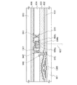
本実施の形態では、実施の形態1で説明した光検出装置1300の積層構成の一例について説明する。なお、本実施の形態では、検出器1301としてフォトダイオードを用いる例について説明する。図2は光検出装置1300の一部を示す断面図である。
本実施の形態では、実施の形態1に示したアナログ回路が有する薄膜トランジスタの一例について示す。
本実施の形態では、実施の形態1に示したアナログ回路が有する薄膜トランジスタの一例について示す。なお、実施の形態3と同一部分又は同様な機能を有する部分、及び工程は、実施の形態3と同様とすればよく、その繰り返しの説明は省略する。また同じ箇所の詳細な説明も省略する。
本実施の形態では、実施の形態1に示したアナログ回路が有する薄膜トランジスタの一例について示す。なお、他の実施の形態の内容と同一部分または同様な機能を有する部分、及び工程は、他の実施の形態と同様とすればよく、その繰り返しの説明は省略する。また同じ箇所の詳細な説明も省略する。
本実施の形態では、実施の形態1に示したアナログ回路が有する薄膜トランジスタの一例について示す。
本実施の形態では、実施の形態1に示したアナログ回路が有する薄膜トランジスタの一例について示す。
本実施の形態では、実施の形態1に示したアナログ回路が有する薄膜トランジスタの一例について示す。
本実施の形態では、実施の形態1に示したアナログ回路が有する薄膜トランジスタの一例について示す。
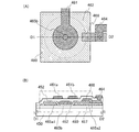
本実施の形態では、実施の形態1に示したアナログ回路を有する半導体装置の一例について説明する。具体的には、実施の形態1に示した光検出装置を有する液晶表示パネルの外観及び断面について、図12を用いて説明する。図12は、薄膜トランジスタ4010、薄膜トランジスタ4011、及び液晶素子4013を、第1の基板4001と第2の基板4006との間にシール材4005によって封止したパネル上面図であり、図12(B)は、図12(A)または図12(C)のM−Nにおける断面図に相当する。
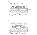
本実施の形態では、アクティブマトリクス型の発光表示装置の一例を示す。なお、具体的には、エレクトロルミネッセンスを利用する発光素子を有する発光表示装置の一例について説明する。
本実施の形態では、本明細書で開示する半導体装置の一形態について説明する。具体的には、本明細書で開示する半導体装置の一形態として、電子ペーパーの例を示す。
本明細書に開示する半導体装置は、さまざまな電子機器(遊技機も含む)に適用することができる。電子機器としては、例えば、テレビジョン装置(テレビ、またはテレビジョン受信機ともいう)、コンピュータ用などのモニタ、デジタルカメラ、デジタルビデオカメラ、デジタルフォトフレーム、携帯電話機(携帯電話、携帯電話装置ともいう)、携帯型ゲーム機、携帯情報端末、音響再生装置、パチンコ機などの大型ゲーム機などが挙げられる。
本明細書に開示する半導体装置は、電子ペーパーとして適用することができる。電子ペーパーは、情報を表示するものであればあらゆる分野の電子機器に用いることが可能である。例えば、電子ペーパーを用いて、電子書籍(電子ブック)、ポスター、電車などの乗り物の車内広告、クレジットカード等の各種カードにおける表示等に適用することができる。電子機器の一例を図21に示す。
302 ゲート絶縁層
303 保護絶縁層
310 薄膜トランジスタ
311 ゲート電極層
316 酸化物絶縁層
320 基板
322 ゲート絶縁層
323 保護絶縁層
330 酸化物半導体膜
331 酸化物半導体層
332 酸化物半導体層
340 基板
342 ゲート絶縁層
343 保護絶縁層
345 酸化物半導体膜
346 酸化物半導体層
350 薄膜トランジスタ
351 ゲート電極層
356 酸化物絶縁層
360 薄膜トランジスタ
361 ゲート電極層
366 酸化物絶縁層
370 基板
373 保護絶縁層
380 薄膜トランジスタ
381 ゲート電極層
382 酸化物半導体層
386 酸化物絶縁層
400 基板
402 ゲート絶縁層
403 保護絶縁層
407 絶縁層
409 平坦化絶縁層
410 薄膜トランジスタ
411 ゲート電極層
412 酸化物半導体層
416 酸化物絶縁層
420 シリコン基板
422 絶縁層
423 開口
424 導電層
425 薄膜トランジスタ
426 薄膜トランジスタ
427 導電層
430 酸化物半導体膜
438 配線層
450 基板
452 ゲート絶縁層
457 絶縁層
460 薄膜トランジスタ
461 ゲート電極層
462 酸化物半導体層
464 配線層
468 配線層
580 基板
581 薄膜トランジスタ
583 酸化シリコン層
584 保護絶縁層
585 絶縁層
587 電極層
588 電極層
589 球形粒子
594 キャビティ
595 充填材
596 対向基板
601 基板
608 接着層
613 基板
622 光
631 絶縁層
632 保護絶縁層
633 層間絶縁層
634 層間絶縁層
641 電極層
642 電極層
643 導電層
644 電極層
645 ゲート電極層
1300 光検出装置
1301 検出器
1302 増幅回路
1305 トランジスタ
1306 トランジスタ
1311 電源端子
1312 電源端子
1320 保護回路
1321 ダイオード
1600 携帯電話機
1601 筐体
1602 表示部
1604 外部接続ポート
1605 スピーカー
1606 マイク
1800 筐体
1801 筐体
1802 表示パネル
1803 スピーカー
1804 マイクロフォン
1805 操作キー
1806 ポインティングデバイス
1807 カメラ用レンズ
1808 外部接続端子
1810 キーボード
1811 外部メモリスロット
2700 電子書籍
2701 筐体
2703 筐体
2705 表示部
2707 表示部
2711 軸部
2721 電源
2723 操作キー
2725 スピーカー
4001 基板
4002 画素部
4003 信号線駆動回路
4004 走査線駆動回路
4005 シール材
4006 基板
4008 液晶層
4010 薄膜トランジスタ
4011 薄膜トランジスタ
4013 液晶素子
4015 接続端子電極
4016 端子電極
4018 FPC
4019 異方性導電膜
4020 絶縁層
4021 絶縁層
4030 画素電極層
4031 対向電極層
4032 絶縁層
4033 絶縁層
4035 スペーサ
4040 導電層
4041 絶縁層
4042 保護絶縁層
4100 光検出装置
4501 基板
4502 画素部
4505 シール材
4506 基板
4507 充填材
4509 薄膜トランジスタ
4510 薄膜トランジスタ
4511 発光素子
4512 電界発光層
4513 電極
4515 接続端子電極
4516 端子電極
4517 電極
4519 異方性導電膜
4520 隔壁
4540 導電層
4542 酸化シリコン層
4543 オーバーコート層
4544 絶縁層
4545 カラーフィルタ層
4550 配線層
4551 絶縁層
4580 光検出装置
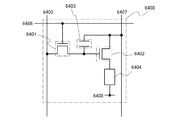
6400 画素
6401 スイッチング用トランジスタ
6402 発光素子駆動用トランジスタ
6403 容量素子
6404 発光素子
6405 信号線
6406 走査線
6407 電源線
6408 共通電極
6502 発光素子駆動用トランジスタ
6503 容量素子
6504 発光素子
6505 信号線
6506 走査線
6507 電源線
6508 共通電極
6510 画素
6511 スイッチング用トランジスタ
6512 スイッチング用トランジスタ
6513 参照トランジスタ
7001 発光素子駆動用トランジスタ
7002 発光素子
7003 電極
7004 EL層
7005 電極
7009 隔壁
7011 発光素子駆動用トランジスタ
7012 発光素子
7013 電極
7014 EL層
7015 電極
7016 遮蔽膜
7017 導電膜
7019 隔壁
7021 発光素子駆動用トランジスタ
7022 発光素子
7023 電極
7024 EL層
7025 電極
7027 導電膜
7029 隔壁
7031 絶縁層
7032 絶縁層
7033 カラーフィルタ層
7034 オーバーコート層
7035 保護絶縁層
7036 平坦化絶縁層
7041 絶縁層
7042 絶縁層
7043 カラーフィルタ層
7044 オーバーコート層
7045 保護絶縁層
7046 平坦化絶縁層
7051 酸化シリコン層
7052 保護絶縁層
7053 平坦化絶縁層
7055 絶縁層
7056 平坦化絶縁層
9600 テレビジョン装置
9601 筐体
9603 表示部
9605 スタンド
9607 表示部
9609 操作キー
9610 リモコン操作機
9700 デジタルフォトフレーム
9701 筐体
9703 表示部
9881 筐体
9882 表示部
9883 表示部
9884 スピーカー部
9885 操作キー
9886 記録媒体挿入部
9887 接続端子
9888 センサ
9889 マイクロフォン
9890 LEDランプ
9891 筐体
9893 連結部
1603a 操作ボタン
1603b 操作ボタン
315a ソース電極層
315b ドレイン電極層
355a ソース電極層
355b ドレイン電極層
365a ソース電極層
365b ドレイン電極層
372a ゲート絶縁層
372b ゲート絶縁層
385a ソース電極層
385b ドレイン電極層
414a 配線層
414b 配線層
415a ドレイン電極層
415b ドレイン電極層
421a 開口
421b 開口
4503a 信号線駆動回路
4503b 信号線駆動回路
4504a 走査線駆動回路
4504b 走査線駆動回路
4518a FPC
4518b FPC
465a ソース電極層又はドレイン電極層
465a1 ソース電極層又はドレイン電極層
465a2 ソース電極層又はドレイン電極層
465b ソース電極層又はドレイン電極層
590a 黒色領域
590b 白色領域
606a 半導体層
606b 半導体層
606c 半導体層
Claims (10)
- リファレンストランジスタと、ミラートランジスタと、検出器と、を有し、
前記リファレンストランジスタは前記検出器と電気的に接続され、
前記リファレンストランジスタのドレインとゲートは電気的に接続され、
前記リファレンストランジスタのゲートは前記ミラートランジスタのゲートと電気的に接続され、
前記リファレンストランジスタと前記ミラートランジスタは、ドレイン電圧が1V及び10Vの場合において、ゲート電圧が−5Vから−20Vの範囲におけるドレイン電流が1×10 −13 A以下である酸化物半導体を有することを特徴とするアナログ回路。 - 請求項1において、
前記ミラートランジスタは、複数の薄膜トランジスタが並列接続されていることを特徴とするアナログ回路。 - 請求項1または請求項2において、
前記ミラートランジスタのチャネル幅は、前記リファレンストランジスタのチャネル幅よりも大きいことを特徴とするアナログ回路。 - 請求項1乃至請求項3のいずれか一項において、
前記酸化物半導体のチャネル領域のキャリア濃度が5×10¹⁴/cm3以下であることを特徴とするアナログ回路。 - 請求項1乃至請求項4のいずれか一項において、
前記酸化物半導体のチャネル領域の水素濃度が5×10 19 atoms/cm 3 以下であることを特徴とするアナログ回路。 - 第1端子が高電源電位に電気的に接続された第1の薄膜トランジスタと、
第1端子が高電源電位に電気的に接続された第2の薄膜トランジスタと、
前記高電源電位と、前記第1の薄膜トランジスタの前記第1端子との間に、検出器と、を有し、
前記第1の薄膜トランジスタのゲートは、前記検出器と前記第1の薄膜トランジスタの前記第1端子の間に電気的に接続され、
前記第2の薄膜トランジスタのゲートは、前記第1の薄膜トランジスタのゲートと電気的に接続され、
前記第1の薄膜トランジスタの第2端子と、前記第2の薄膜トランジスタの第2端子とは、低電源電位に電気的に接続され、
前記第1の薄膜トランジスタと前記第2の薄膜トランジスタは、ドレイン電圧が1V及び10Vの場合において、ゲート電圧が−5Vから−20Vの範囲におけるドレイン電流が1×10 −13 A以下である酸化物半導体を有することを特徴とするアナログ回路。 - 請求項6において、
前記第2の薄膜トランジスタは、複数の薄膜トランジスタが並列接続されていることを特徴とするアナログ回路。 - 請求項6または請求項7において、
前記第2の薄膜トランジスタのチャネル幅は、前記第1の薄膜トランジスタのチャネル幅よりも大きいことを特徴とするアナログ回路。 - 請求項6乃至請求項8のいずれか一項において、
前記酸化物半導体のチャネル領域のキャリア濃度が5×10¹⁴/cm3以下であることを特徴とするアナログ回路。 - 請求項6乃至請求項9のいずれか一項において、
前記酸化物半導体のチャネル領域の水素濃度が5×10 19 atoms/cm 3 以下であることを特徴とするアナログ回路。
Priority Applications (1)
| Application Number | Priority Date | Filing Date | Title |
|---|---|---|---|
| JP2010231402A JP5489946B2 (ja) | 2009-10-21 | 2010-10-14 | アナログ回路 |
Applications Claiming Priority (3)
| Application Number | Priority Date | Filing Date | Title |
|---|---|---|---|
| JP2009242853 | 2009-10-21 | ||
| JP2009242853 | 2009-10-21 | ||
| JP2010231402A JP5489946B2 (ja) | 2009-10-21 | 2010-10-14 | アナログ回路 |
Related Child Applications (1)
| Application Number | Title | Priority Date | Filing Date |
|---|---|---|---|
| JP2014033928A Division JP5740019B2 (ja) | 2009-10-21 | 2014-02-25 | 半導体装置 |
Publications (3)
| Publication Number | Publication Date |
|---|---|
| JP2011109646A JP2011109646A (ja) | 2011-06-02 |
| JP2011109646A5 JP2011109646A5 (ja) | 2013-10-17 |
| JP5489946B2 true JP5489946B2 (ja) | 2014-05-14 |
Family
ID=43878834
Family Applications (12)
| Application Number | Title | Priority Date | Filing Date |
|---|---|---|---|
| JP2010231402A Expired - Fee Related JP5489946B2 (ja) | 2009-10-21 | 2010-10-14 | アナログ回路 |
| JP2014033928A Active JP5740019B2 (ja) | 2009-10-21 | 2014-02-25 | 半導体装置 |
| JP2015088976A Active JP6009030B2 (ja) | 2009-10-21 | 2015-04-24 | 半導体装置 |
| JP2016178414A Withdrawn JP2017027065A (ja) | 2009-10-21 | 2016-09-13 | 半導体装置 |
| JP2018097727A Active JP6578039B2 (ja) | 2009-10-21 | 2018-05-22 | 表示装置 |
| JP2018133999A Active JP6506873B2 (ja) | 2009-10-21 | 2018-07-17 | 半導体装置 |
| JP2019066951A Withdrawn JP2019145509A (ja) | 2009-10-21 | 2019-03-29 | 半導体装置 |
| JP2019152544A Active JP6832994B2 (ja) | 2009-10-21 | 2019-08-23 | トランジスタ及び半導体装置 |
| JP2021014898A Active JP7092904B2 (ja) | 2009-10-21 | 2021-02-02 | 半導体装置 |
| JP2022097250A Active JP7398515B2 (ja) | 2009-10-21 | 2022-06-16 | 半導体装置 |
| JP2023204628A Withdrawn JP2024036316A (ja) | 2009-10-21 | 2023-12-04 | 半導体装置 |
| JP2025093053A Pending JP2025123249A (ja) | 2009-10-21 | 2025-06-04 | 半導体装置 |
Family Applications After (11)
| Application Number | Title | Priority Date | Filing Date |
|---|---|---|---|
| JP2014033928A Active JP5740019B2 (ja) | 2009-10-21 | 2014-02-25 | 半導体装置 |
| JP2015088976A Active JP6009030B2 (ja) | 2009-10-21 | 2015-04-24 | 半導体装置 |
| JP2016178414A Withdrawn JP2017027065A (ja) | 2009-10-21 | 2016-09-13 | 半導体装置 |
| JP2018097727A Active JP6578039B2 (ja) | 2009-10-21 | 2018-05-22 | 表示装置 |
| JP2018133999A Active JP6506873B2 (ja) | 2009-10-21 | 2018-07-17 | 半導体装置 |
| JP2019066951A Withdrawn JP2019145509A (ja) | 2009-10-21 | 2019-03-29 | 半導体装置 |
| JP2019152544A Active JP6832994B2 (ja) | 2009-10-21 | 2019-08-23 | トランジスタ及び半導体装置 |
| JP2021014898A Active JP7092904B2 (ja) | 2009-10-21 | 2021-02-02 | 半導体装置 |
| JP2022097250A Active JP7398515B2 (ja) | 2009-10-21 | 2022-06-16 | 半導体装置 |
| JP2023204628A Withdrawn JP2024036316A (ja) | 2009-10-21 | 2023-12-04 | 半導体装置 |
| JP2025093053A Pending JP2025123249A (ja) | 2009-10-21 | 2025-06-04 | 半導体装置 |
Country Status (5)
| Country | Link |
|---|---|
| US (10) | US8242837B2 (ja) |
| JP (12) | JP5489946B2 (ja) |
| KR (7) | KR102223581B1 (ja) |
| TW (3) | TWI612677B (ja) |
| WO (1) | WO2011049005A1 (ja) |
Families Citing this family (62)
| Publication number | Priority date | Publication date | Assignee | Title |
|---|---|---|---|---|
| JP5407638B2 (ja) * | 2009-07-28 | 2014-02-05 | セイコーエプソン株式会社 | アクティブマトリクス基板、電気光学装置、及び電子機器 |
| CN102598280B (zh) | 2009-10-21 | 2016-05-18 | 株式会社半导体能源研究所 | 液晶显示器件及包括该液晶显示器件的电子设备 |
| KR101810254B1 (ko) * | 2009-11-06 | 2017-12-18 | 가부시키가이샤 한도오따이 에네루기 켄큐쇼 | 반도체 장치 및 그 동작 방법 |
| WO2011077926A1 (en) * | 2009-12-24 | 2011-06-30 | Semiconductor Energy Laboratory Co., Ltd. | Display device and electronic device |
| CN102754022B (zh) | 2010-02-26 | 2016-11-09 | 株式会社半导体能源研究所 | 液晶显示装置 |
| US8969132B2 (en) * | 2010-09-20 | 2015-03-03 | Nuvotronics, Llc | Device package and methods for the fabrication thereof |
| JP5647860B2 (ja) * | 2010-10-28 | 2015-01-07 | 富士フイルム株式会社 | 薄膜トランジスタおよびその製造方法 |
| KR101793073B1 (ko) * | 2010-12-06 | 2017-11-03 | 삼성디스플레이 주식회사 | 터치 스크린 패널 |
| US9960278B2 (en) * | 2011-04-06 | 2018-05-01 | Yuhei Sato | Manufacturing method of semiconductor device |
| KR101919056B1 (ko) * | 2011-04-28 | 2018-11-15 | 가부시키가이샤 한도오따이 에네루기 켄큐쇼 | 반도체 회로 |
| US8709922B2 (en) * | 2011-05-06 | 2014-04-29 | Semiconductor Energy Laboratory Co., Ltd. | Semiconductor device |
| US8946066B2 (en) * | 2011-05-11 | 2015-02-03 | Semiconductor Energy Laboratory Co., Ltd. | Method of manufacturing semiconductor device |
| US9048788B2 (en) * | 2011-05-13 | 2015-06-02 | Semiconductor Energy Laboratory Co., Ltd. | Semiconductor device comprising a photoelectric conversion portion |
| US8673426B2 (en) * | 2011-06-29 | 2014-03-18 | Semiconductor Energy Laboratory Co., Ltd. | Driver circuit, method of manufacturing the driver circuit, and display device including the driver circuit |
| US8710615B2 (en) * | 2011-08-31 | 2014-04-29 | Infineon Technologies Ag | Semiconductor device with an amorphous semi-insulating layer, temperature sensor, and method of manufacturing a semiconductor device |
| US9419146B2 (en) | 2012-01-26 | 2016-08-16 | Semiconductor Energy Laboratory Co., Ltd. | Semiconductor device and method for manufacturing the same |
| TWI484626B (zh) * | 2012-02-21 | 2015-05-11 | 璨圓光電股份有限公司 | 半導體發光元件及具有此半導體發光元件的發光裝置 |
| KR20130125717A (ko) * | 2012-05-09 | 2013-11-19 | 가부시키가이샤 한도오따이 에네루기 켄큐쇼 | 반도체 장치 및 그 구동 방법 |
| KR20130136063A (ko) | 2012-06-04 | 2013-12-12 | 삼성디스플레이 주식회사 | 박막 트랜지스터, 이를 포함하는 박막 트랜지스터 표시판 및 그 제조 방법 |
| TWI596778B (zh) * | 2012-06-29 | 2017-08-21 | 半導體能源研究所股份有限公司 | 半導體裝置及半導體裝置的製造方法 |
| US10134852B2 (en) | 2012-06-29 | 2018-11-20 | Semiconductor Energy Laboratory Co., Ltd. | Semiconductor device |
| US9337152B2 (en) | 2013-03-15 | 2016-05-10 | Nuvotronics, Inc | Formulation for packaging an electronic device and assemblies made therefrom |
| KR102207563B1 (ko) * | 2013-10-29 | 2021-01-27 | 삼성디스플레이 주식회사 | 유기 발광 표시장치 및 유기 발광 표시장치의 제조 방법 |
| TWI527201B (zh) * | 2013-11-06 | 2016-03-21 | 友達光電股份有限公司 | 畫素結構及其製造方法 |
| TWI686899B (zh) * | 2014-05-02 | 2020-03-01 | 日商半導體能源研究所股份有限公司 | 半導體裝置、觸控感測器、顯示裝置 |
| KR102333604B1 (ko) | 2014-05-15 | 2021-11-30 | 가부시키가이샤 한도오따이 에네루기 켄큐쇼 | 반도체 장치, 이 반도체 장치를 포함하는 표시 장치 |
| US9633710B2 (en) | 2015-01-23 | 2017-04-25 | Semiconductor Energy Laboratory Co., Ltd. | Method for operating semiconductor device |
| US9653613B2 (en) * | 2015-02-27 | 2017-05-16 | Semiconductor Energy Laboratory Co., Ltd. | Semiconductor device and manufacturing method thereof |
| US10163948B2 (en) * | 2015-07-23 | 2018-12-25 | Semiconductor Energy Laboratory Co., Ltd. | Imaging device and electronic device |
| CN108352358B (zh) | 2015-10-13 | 2022-07-26 | 非结晶公司 | 非晶金属薄膜非线性电阻器 |
| US10797113B2 (en) | 2016-01-25 | 2020-10-06 | Semiconductor Energy Laboratory Co., Ltd. | Light-emitting device with layered electrode structures |
| US10242244B2 (en) * | 2016-01-27 | 2019-03-26 | Japan Display Inc. | Fingerprint detection device and display device |
| CN108573983B (zh) * | 2017-03-13 | 2021-08-17 | 京东方科技集团股份有限公司 | 光学探测器及其制备方法、指纹识别传感器、显示装置 |
| US10475586B2 (en) * | 2017-03-31 | 2019-11-12 | Tdk Corporation | Oxynitride thin film and capacitance element |
| US10479732B2 (en) * | 2017-03-31 | 2019-11-19 | Tdk Corporation | Oxynitride thin film and capacitance element |
| CN108987411A (zh) * | 2017-06-02 | 2018-12-11 | 京东方科技集团股份有限公司 | 阵列基板及其制备方法和显示装置 |
| CN107731973B (zh) * | 2017-10-30 | 2019-03-12 | 厦门乾照光电股份有限公司 | 一种led芯片及制作方法 |
| CN108199774A (zh) * | 2018-01-11 | 2018-06-22 | 中国电子科技集团公司第四十四研究所 | 一种基于红外led光纤的数据通信设备及其制造方法和通信方法 |
| CN108540600B (zh) * | 2018-03-30 | 2020-09-18 | Oppo广东移动通信有限公司 | 电子装置 |
| CN111919302B (zh) | 2018-03-30 | 2025-01-14 | 非结晶公司 | 非晶金属薄膜晶体管 |
| CN110579525B (zh) * | 2018-06-08 | 2023-08-18 | 天马日本株式会社 | 传感器装置 |
| US11935961B2 (en) | 2018-10-18 | 2024-03-19 | Semiconductor Energy Laboratory Co., Ltd. | Semiconductor device, semiconductor wafer, and electronic device |
| CN109860265B (zh) * | 2019-03-06 | 2021-10-01 | 京东方科技集团股份有限公司 | 一种基板及其制备方法、显示面板、显示装置 |
| TWI705412B (zh) * | 2019-03-22 | 2020-09-21 | 台灣奈米碳素股份有限公司 | 基於氣體評價食材風味的系統及方法 |
| US10777153B1 (en) * | 2019-05-16 | 2020-09-15 | Himax Display, Inc. | Method for calculating pixel voltage for liquid crystal on silicon display device |
| KR102830608B1 (ko) | 2019-08-07 | 2025-07-08 | 가부시끼가이샤 레조낙 | 유중수형 유화 조성물 |
| JP2021026187A (ja) * | 2019-08-08 | 2021-02-22 | 株式会社ジャパンディスプレイ | 表示装置 |
| CN110600488B (zh) * | 2019-10-12 | 2025-03-28 | 京东方科技集团股份有限公司 | 一种氧化物薄膜晶体管及其驱动方法、显示装置 |
| US11379231B2 (en) | 2019-10-25 | 2022-07-05 | Semiconductor Energy Laboratory Co., Ltd. | Data processing system and operation method of data processing system |
| KR102859780B1 (ko) * | 2019-12-10 | 2025-09-15 | 삼성디스플레이 주식회사 | 발광 소자 및 이를 포함하는 표시 장치 |
| KR20210113531A (ko) * | 2020-03-06 | 2021-09-16 | 삼성디스플레이 주식회사 | 표시 장치 |
| CN111430386B (zh) * | 2020-04-01 | 2023-11-10 | 京东方科技集团股份有限公司 | 光电探测器、显示基板及光电探测器的制作方法 |
| CN115606010B (zh) * | 2020-06-11 | 2025-07-15 | 苏州晶湛半导体有限公司 | 半导体结构及其制作方法 |
| JP7803887B2 (ja) | 2020-06-12 | 2026-01-21 | アモルフィックス・インコーポレイテッド | 電子デバイスのための非線形構成要素を含む回路 |
| CN111883063B (zh) * | 2020-07-17 | 2021-11-12 | 合肥维信诺科技有限公司 | 像素电路、显示面板及显示装置 |
| US11349304B2 (en) * | 2020-10-28 | 2022-05-31 | Globalfoundries U.S. Inc. | Structure and method for controlling electrostatic discharge (ESD) event in resistor-capacitor circuit |
| CN114864760B (zh) * | 2021-02-03 | 2024-12-13 | 厦门三安光电有限公司 | 微型发光二极管和显示面板 |
| EP4164003A4 (en) | 2021-02-23 | 2024-03-27 | LG Energy Solution, Ltd. | SACRIFICIAL POSITIVE ELECTRODE MATERIAL WITH REDUCED GAS GENERATION AND METHOD FOR PRODUCING THEREOF |
| US11900859B2 (en) | 2021-05-21 | 2024-02-13 | Lumileds Llc | Active matrix hybrid microLED display |
| CN113484703B (zh) * | 2021-06-25 | 2022-08-12 | 成都飞机工业(集团)有限责任公司 | 一种空气式静电放电的测试方法及测试设备 |
| CN117074890A (zh) * | 2022-05-09 | 2023-11-17 | 星科金朋私人有限公司 | 测试半导体器件的方法和装置 |
| US12561033B2 (en) | 2024-07-08 | 2026-02-24 | Apple Inc. | Capacitive touch sensing with reduced ambient light interference |
Family Cites Families (239)
| Publication number | Priority date | Publication date | Assignee | Title |
|---|---|---|---|---|
| JPS60198861A (ja) | 1984-03-23 | 1985-10-08 | Fujitsu Ltd | 薄膜トランジスタ |
| JPH0244256B2 (ja) | 1987-01-28 | 1990-10-03 | Kagaku Gijutsucho Mukizaishitsu Kenkyushocho | Ingazn2o5deshimesarerurotsuhoshokeinosojokozoojusurukagobutsuoyobisonoseizoho |
| JPH0244260B2 (ja) | 1987-02-24 | 1990-10-03 | Kagaku Gijutsucho Mukizaishitsu Kenkyushocho | Ingazn5o8deshimesarerurotsuhoshokeinosojokozoojusurukagobutsuoyobisonoseizoho |
| JPH0244258B2 (ja) | 1987-02-24 | 1990-10-03 | Kagaku Gijutsucho Mukizaishitsu Kenkyushocho | Ingazn3o6deshimesarerurotsuhoshokeinosojokozoojusurukagobutsuoyobisonoseizoho |
| JPS63210023A (ja) | 1987-02-24 | 1988-08-31 | Natl Inst For Res In Inorg Mater | InGaZn↓4O↓7で示される六方晶系の層状構造を有する化合物およびその製造法 |
| JPH0244262B2 (ja) | 1987-02-27 | 1990-10-03 | Kagaku Gijutsucho Mukizaishitsu Kenkyushocho | Ingazn6o9deshimesarerurotsuhoshokeinosojokozoojusurukagobutsuoyobisonoseizoho |
| JPH0244263B2 (ja) | 1987-04-22 | 1990-10-03 | Kagaku Gijutsucho Mukizaishitsu Kenkyushocho | Ingazn7o10deshimesarerurotsuhoshokeinosojokozoojusurukagobutsuoyobisonoseizoho |
| DE68901666T2 (de) | 1988-03-15 | 1993-02-11 | Aleados Del Cobres S A Alecosa | Waermebehaelter fuer fluessigkeiten, fette produkte, gele und aehnliches. |
| JPH0229543U (ja) * | 1988-08-15 | 1990-02-26 | ||
| JPH05251705A (ja) | 1992-03-04 | 1993-09-28 | Fuji Xerox Co Ltd | 薄膜トランジスタ |
| JP3156522B2 (ja) * | 1994-09-22 | 2001-04-16 | 凸版印刷株式会社 | 液晶表示装置用駆動回路 |
| JPH08179376A (ja) * | 1994-12-22 | 1996-07-12 | Sony Corp | カラー表示装置 |
| JP2768321B2 (ja) * | 1995-02-28 | 1998-06-25 | 日本電気株式会社 | 半導体記憶装置 |
| JP3479375B2 (ja) | 1995-03-27 | 2003-12-15 | 科学技術振興事業団 | 亜酸化銅等の金属酸化物半導体による薄膜トランジスタとpn接合を形成した金属酸化物半導体装置およびそれらの製造方法 |
| DE69635107D1 (de) * | 1995-08-03 | 2005-09-29 | Koninkl Philips Electronics Nv | Halbleiteranordnung mit einem transparenten schaltungselement |
| JP3625598B2 (ja) * | 1995-12-30 | 2005-03-02 | 三星電子株式会社 | 液晶表示装置の製造方法 |
| JP3145931B2 (ja) * | 1996-08-26 | 2001-03-12 | 日本電気株式会社 | 薄膜トランジスタ |
| JP3264364B2 (ja) * | 1997-01-21 | 2002-03-11 | シャープ株式会社 | 液晶表示装置の製造方法 |
| JP3702096B2 (ja) * | 1998-06-08 | 2005-10-05 | 三洋電機株式会社 | 薄膜トランジスタ及び表示装置 |
| JP4170454B2 (ja) | 1998-07-24 | 2008-10-22 | Hoya株式会社 | 透明導電性酸化物薄膜を有する物品及びその製造方法 |
| JP2000150861A (ja) * | 1998-11-16 | 2000-05-30 | Tdk Corp | 酸化物薄膜 |
| JP3276930B2 (ja) * | 1998-11-17 | 2002-04-22 | 科学技術振興事業団 | トランジスタ及び半導体装置 |
| US8853696B1 (en) | 1999-06-04 | 2014-10-07 | Semiconductor Energy Laboratory Co., Ltd. | Electro-optical device and electronic device |
| KR100888004B1 (ko) | 1999-07-14 | 2009-03-09 | 소니 가부시끼 가이샤 | 전류 구동 회로 및 그것을 사용한 표시 장치, 화소 회로,및 구동 방법 |
| US7379039B2 (en) | 1999-07-14 | 2008-05-27 | Sony Corporation | Current drive circuit and display device using same pixel circuit, and drive method |
| TW460731B (en) * | 1999-09-03 | 2001-10-21 | Ind Tech Res Inst | Electrode structure and production method of wide viewing angle LCD |
| CN1170458C (zh) | 2000-03-07 | 2004-10-06 | 出光兴产株式会社 | 有源驱动型有机el显示装置及其制造方法 |
| TW513753B (en) | 2000-03-27 | 2002-12-11 | Semiconductor Energy Lab | Semiconductor display device and manufacturing method thereof |
| JP4089858B2 (ja) | 2000-09-01 | 2008-05-28 | 国立大学法人東北大学 | 半導体デバイス |
| JP4318455B2 (ja) | 2000-10-12 | 2009-08-26 | 三洋電機株式会社 | カラーフィルタ形成方法または発光素子層形成方法またはこれらを利用したカラー表示装置の製造方法またはカラー表示装置 |
| KR20020038482A (ko) * | 2000-11-15 | 2002-05-23 | 모리시타 요이찌 | 박막 트랜지스터 어레이, 그 제조방법 및 그것을 이용한표시패널 |
| US7071771B2 (en) * | 2000-12-11 | 2006-07-04 | Kabushiki Kaisha Toshiba | Current difference divider circuit |
| US6753654B2 (en) | 2001-02-21 | 2004-06-22 | Semiconductor Energy Laboratory Co., Ltd. | Light emitting device and electronic appliance |
| JP4212815B2 (ja) * | 2001-02-21 | 2009-01-21 | 株式会社半導体エネルギー研究所 | 発光装置 |
| JP3997731B2 (ja) * | 2001-03-19 | 2007-10-24 | 富士ゼロックス株式会社 | 基材上に結晶性半導体薄膜を形成する方法 |
| JP2002289859A (ja) | 2001-03-23 | 2002-10-04 | Minolta Co Ltd | 薄膜トランジスタ |
| US6897477B2 (en) | 2001-06-01 | 2005-05-24 | Semiconductor Energy Laboratory Co., Ltd. | Semiconductor device, manufacturing method thereof, and display device |
| JP2005322935A (ja) | 2001-06-01 | 2005-11-17 | Semiconductor Energy Lab Co Ltd | 半導体装置およびその作製方法 |
| US6876350B2 (en) | 2001-08-10 | 2005-04-05 | Semiconductor Energy Laboratory Co., Ltd. | Display device and electronic equipment using the same |
| JP4202069B2 (ja) * | 2001-08-10 | 2008-12-24 | 株式会社半導体エネルギー研究所 | 半導体装置及び表示装置 |
| CN100371962C (zh) | 2001-08-29 | 2008-02-27 | 株式会社半导体能源研究所 | 发光器件、发光器件驱动方法、以及电子设备 |
| JP3813555B2 (ja) * | 2001-08-29 | 2006-08-23 | 株式会社半導体エネルギー研究所 | 発光装置及び電子機器 |
| JP4090716B2 (ja) | 2001-09-10 | 2008-05-28 | 雅司 川崎 | 薄膜トランジスタおよびマトリクス表示装置 |
| JP3925839B2 (ja) | 2001-09-10 | 2007-06-06 | シャープ株式会社 | 半導体記憶装置およびその試験方法 |
| JP3655859B2 (ja) | 2001-09-26 | 2005-06-02 | 東芝マイクロエレクトロニクス株式会社 | 定電流回路 |
| JP2003108070A (ja) * | 2001-09-28 | 2003-04-11 | Sanyo Electric Co Ltd | 表示装置 |
| US7193619B2 (en) | 2001-10-31 | 2007-03-20 | Semiconductor Energy Laboratory Co., Ltd. | Signal line driving circuit and light emitting device |
| JP4164562B2 (ja) | 2002-09-11 | 2008-10-15 | 独立行政法人科学技術振興機構 | ホモロガス薄膜を活性層として用いる透明薄膜電界効果型トランジスタ |
| WO2003040441A1 (fr) * | 2001-11-05 | 2003-05-15 | Japan Science And Technology Agency | Film mince monocristallin homologue a super-reseau naturel, procede de preparation et dispositif dans lequel est utilise ledit film mince monocristallin |
| US20030103022A1 (en) | 2001-11-09 | 2003-06-05 | Yukihiro Noguchi | Display apparatus with function for initializing luminance data of optical element |
| JP2003150105A (ja) * | 2001-11-09 | 2003-05-23 | Sanyo Electric Co Ltd | 表示装置 |
| JP4718761B2 (ja) * | 2002-02-13 | 2011-07-06 | 株式会社半導体エネルギー研究所 | 発光装置の作製方法 |
| US6933520B2 (en) | 2002-02-13 | 2005-08-23 | Semiconductor Energy Laboratory Co., Ltd. | Light emitting device |
| JP4083486B2 (ja) * | 2002-02-21 | 2008-04-30 | 独立行政法人科学技術振興機構 | LnCuO(S,Se,Te)単結晶薄膜の製造方法 |
| JP3613253B2 (ja) * | 2002-03-14 | 2005-01-26 | 日本電気株式会社 | 電流制御素子の駆動回路及び画像表示装置 |
| US7876294B2 (en) | 2002-03-05 | 2011-01-25 | Nec Corporation | Image display and its control method |
| US7049190B2 (en) * | 2002-03-15 | 2006-05-23 | Sanyo Electric Co., Ltd. | Method for forming ZnO film, method for forming ZnO semiconductor layer, method for fabricating semiconductor device, and semiconductor device |
| JP4069648B2 (ja) | 2002-03-15 | 2008-04-02 | カシオ計算機株式会社 | 半導体装置および表示駆動装置 |
| JP3933591B2 (ja) * | 2002-03-26 | 2007-06-20 | 淳二 城戸 | 有機エレクトロルミネッセント素子 |
| US7339187B2 (en) * | 2002-05-21 | 2008-03-04 | State Of Oregon Acting By And Through The Oregon State Board Of Higher Education On Behalf Of Oregon State University | Transistor structures |
| JP2004022625A (ja) * | 2002-06-13 | 2004-01-22 | Murata Mfg Co Ltd | 半導体デバイス及び該半導体デバイスの製造方法 |
| US7105868B2 (en) * | 2002-06-24 | 2006-09-12 | Cermet, Inc. | High-electron mobility transistor with zinc oxide |
| JP4723787B2 (ja) * | 2002-07-09 | 2011-07-13 | シャープ株式会社 | 電界効果型トランジスタ、その製造方法及び画像表示装置 |
| US7067843B2 (en) * | 2002-10-11 | 2006-06-27 | E. I. Du Pont De Nemours And Company | Transparent oxide semiconductor thin film transistors |
| JP3702879B2 (ja) | 2003-02-21 | 2005-10-05 | セイコーエプソン株式会社 | 電気光学パネル、その駆動回路及び駆動方法、並びに電子機器 |
| JP4461687B2 (ja) | 2003-02-21 | 2010-05-12 | セイコーエプソン株式会社 | 電気光学パネル、その駆動回路及び駆動方法、並びに電子機器 |
| JP4166105B2 (ja) | 2003-03-06 | 2008-10-15 | シャープ株式会社 | 半導体装置およびその製造方法 |
| JP2004273732A (ja) | 2003-03-07 | 2004-09-30 | Sharp Corp | アクティブマトリクス基板およびその製造方法 |
| KR100742063B1 (ko) | 2003-05-26 | 2007-07-23 | 가시오게산키 가부시키가이샤 | 전류생성공급회로 및 표시장치 |
| JP4019321B2 (ja) * | 2003-06-04 | 2007-12-12 | カシオ計算機株式会社 | 電流生成供給回路 |
| JP4108633B2 (ja) * | 2003-06-20 | 2008-06-25 | シャープ株式会社 | 薄膜トランジスタおよびその製造方法ならびに電子デバイス |
| TWI228384B (en) | 2003-06-26 | 2005-02-21 | Ind Tech Res Inst | Active matrix organic light emitting diode |
| KR20050005610A (ko) * | 2003-07-05 | 2005-01-14 | 권태인 | 수신단계에서 광고 등이 삽입되는 방송서비스시스템 |
| US7262463B2 (en) * | 2003-07-25 | 2007-08-28 | Hewlett-Packard Development Company, L.P. | Transistor including a deposited channel region having a doped portion |
| US8937580B2 (en) | 2003-08-08 | 2015-01-20 | Semiconductor Energy Laboratory Co., Ltd. | Driving method of light emitting device and light emitting device |
| JP2005084416A (ja) * | 2003-09-09 | 2005-03-31 | Sharp Corp | アクティブマトリクス基板およびそれを用いた表示装置 |
| CA2443206A1 (en) * | 2003-09-23 | 2005-03-23 | Ignis Innovation Inc. | Amoled display backplanes - pixel driver circuits, array architecture, and external compensation |
| JP2007506145A (ja) | 2003-09-23 | 2007-03-15 | イグニス イノベーション インコーポレーテッド | 発光ピクセルのアレイを駆動する回路及び方法 |
| JP4528101B2 (ja) * | 2003-11-26 | 2010-08-18 | ローム株式会社 | D/a変換回路、有機el駆動回路および有機el表示装置 |
| TWI250823B (en) * | 2003-11-26 | 2006-03-01 | Rohm Co Ltd | D/A converter circuit, organic EL drive circuit and organic EL display device |
| JP4295075B2 (ja) * | 2003-12-05 | 2009-07-15 | 日本電信電話株式会社 | 光・電気変換回路および電界検出光学装置 |
| JP4884674B2 (ja) * | 2004-01-16 | 2012-02-29 | 株式会社半導体エネルギー研究所 | 表示装置の作製方法 |
| US7825021B2 (en) | 2004-01-16 | 2010-11-02 | Semiconductor Energy Laboratory Co., Ltd. | Method for manufacturing display device |
| US7381579B2 (en) | 2004-02-26 | 2008-06-03 | Samsung Sdi Co., Ltd. | Donor sheet, method of manufacturing the same, method of manufacturing TFT using the donor sheet, and method of manufacturing flat panel display device using the donor sheet |
| KR100625999B1 (ko) | 2004-02-26 | 2006-09-20 | 삼성에스디아이 주식회사 | 도너 시트, 상기 도너 시트의 제조방법, 상기 도너 시트를이용한 박막 트랜지스터의 제조방법, 및 상기 도너 시트를이용한 평판 표시장치의 제조방법 |
| EP1737044B1 (en) * | 2004-03-12 | 2014-12-10 | Japan Science and Technology Agency | Amorphous oxide and thin film transistor |
| US7297977B2 (en) | 2004-03-12 | 2007-11-20 | Hewlett-Packard Development Company, L.P. | Semiconductor device |
| US7282782B2 (en) * | 2004-03-12 | 2007-10-16 | Hewlett-Packard Development Company, L.P. | Combined binary oxide semiconductor device |
| US7145174B2 (en) * | 2004-03-12 | 2006-12-05 | Hewlett-Packard Development Company, Lp. | Semiconductor device |
| JP5222455B2 (ja) * | 2004-04-28 | 2013-06-26 | 株式会社半導体エネルギー研究所 | 表示装置 |
| US7692378B2 (en) | 2004-04-28 | 2010-04-06 | Semiconductor Energy Laboratory Co., Ltd. | Display device including an insulating layer with an opening |
| US7211825B2 (en) * | 2004-06-14 | 2007-05-01 | Yi-Chi Shih | Indium oxide-based thin film transistors and circuits |
| JP2006005116A (ja) | 2004-06-17 | 2006-01-05 | Casio Comput Co Ltd | 膜形成方法、半導体膜、及び積層絶縁膜 |
| JP4315874B2 (ja) * | 2004-07-30 | 2009-08-19 | 三洋電機株式会社 | 有機エレクトロルミネッセント素子及び有機エレクトロルミネッセント表示装置 |
| US20060289882A1 (en) | 2004-07-30 | 2006-12-28 | Kazuki Nishimura | Organic electroluminescent element and organic electroluminescent display device |
| EP1624333B1 (en) | 2004-08-03 | 2017-05-03 | Semiconductor Energy Laboratory Co., Ltd. | Display device, manufacturing method thereof, and television set |
| JP2006100760A (ja) * | 2004-09-02 | 2006-04-13 | Casio Comput Co Ltd | 薄膜トランジスタおよびその製造方法 |
| US7285501B2 (en) * | 2004-09-17 | 2007-10-23 | Hewlett-Packard Development Company, L.P. | Method of forming a solution processed device |
| US7298084B2 (en) * | 2004-11-02 | 2007-11-20 | 3M Innovative Properties Company | Methods and displays utilizing integrated zinc oxide row and column drivers in conjunction with organic light emitting diodes |
| US7791072B2 (en) * | 2004-11-10 | 2010-09-07 | Canon Kabushiki Kaisha | Display |
| US7829444B2 (en) * | 2004-11-10 | 2010-11-09 | Canon Kabushiki Kaisha | Field effect transistor manufacturing method |
| RU2358354C2 (ru) * | 2004-11-10 | 2009-06-10 | Кэнон Кабусики Кайся | Светоизлучающее устройство |
| US7863611B2 (en) * | 2004-11-10 | 2011-01-04 | Canon Kabushiki Kaisha | Integrated circuits utilizing amorphous oxides |
| US7453065B2 (en) * | 2004-11-10 | 2008-11-18 | Canon Kabushiki Kaisha | Sensor and image pickup device |
| JP5126729B2 (ja) | 2004-11-10 | 2013-01-23 | キヤノン株式会社 | 画像表示装置 |
| JP5138163B2 (ja) | 2004-11-10 | 2013-02-06 | キヤノン株式会社 | 電界効果型トランジスタ |
| JP5118810B2 (ja) | 2004-11-10 | 2013-01-16 | キヤノン株式会社 | 電界効果型トランジスタ |
| CN102945857B (zh) * | 2004-11-10 | 2015-06-03 | 佳能株式会社 | 无定形氧化物和场效应晶体管 |
| WO2006051995A1 (en) * | 2004-11-10 | 2006-05-18 | Canon Kabushiki Kaisha | Field effect transistor employing an amorphous oxide |
| US9275579B2 (en) | 2004-12-15 | 2016-03-01 | Ignis Innovation Inc. | System and methods for extraction of threshold and mobility parameters in AMOLED displays |
| US8599191B2 (en) | 2011-05-20 | 2013-12-03 | Ignis Innovation Inc. | System and methods for extraction of threshold and mobility parameters in AMOLED displays |
| US9280933B2 (en) | 2004-12-15 | 2016-03-08 | Ignis Innovation Inc. | System and methods for extraction of threshold and mobility parameters in AMOLED displays |
| US10012678B2 (en) | 2004-12-15 | 2018-07-03 | Ignis Innovation Inc. | Method and system for programming, calibrating and/or compensating, and driving an LED display |
| US10013907B2 (en) | 2004-12-15 | 2018-07-03 | Ignis Innovation Inc. | Method and system for programming, calibrating and/or compensating, and driving an LED display |
| WO2006063448A1 (en) | 2004-12-15 | 2006-06-22 | Ignis Innovation Inc. | Method and system for programming, calibrating and driving a light emitting device display |
| CA2504571A1 (en) | 2005-04-12 | 2006-10-12 | Ignis Innovation Inc. | A fast method for compensation of non-uniformities in oled displays |
| US8576217B2 (en) | 2011-05-20 | 2013-11-05 | Ignis Innovation Inc. | System and methods for extraction of threshold and mobility parameters in AMOLED displays |
| US9171500B2 (en) | 2011-05-20 | 2015-10-27 | Ignis Innovation Inc. | System and methods for extraction of parasitic parameters in AMOLED displays |
| US20140111567A1 (en) | 2005-04-12 | 2014-04-24 | Ignis Innovation Inc. | System and method for compensation of non-uniformities in light emitting device displays |
| US9799246B2 (en) | 2011-05-20 | 2017-10-24 | Ignis Innovation Inc. | System and methods for extraction of threshold and mobility parameters in AMOLED displays |
| US7579224B2 (en) * | 2005-01-21 | 2009-08-25 | Semiconductor Energy Laboratory Co., Ltd. | Method for manufacturing a thin film semiconductor device |
| TWI505473B (zh) * | 2005-01-28 | 2015-10-21 | 半導體能源研究所股份有限公司 | 半導體裝置,電子裝置,和半導體裝置的製造方法 |
| TWI569441B (zh) * | 2005-01-28 | 2017-02-01 | 半導體能源研究所股份有限公司 | 半導體裝置,電子裝置,和半導體裝置的製造方法 |
| US7858451B2 (en) * | 2005-02-03 | 2010-12-28 | Semiconductor Energy Laboratory Co., Ltd. | Electronic device, semiconductor device and manufacturing method thereof |
| US7948171B2 (en) * | 2005-02-18 | 2011-05-24 | Semiconductor Energy Laboratory Co., Ltd. | Light emitting device |
| US20060197092A1 (en) * | 2005-03-03 | 2006-09-07 | Randy Hoffman | System and method for forming conductive material on a substrate |
| US8681077B2 (en) * | 2005-03-18 | 2014-03-25 | Semiconductor Energy Laboratory Co., Ltd. | Semiconductor device, and display device, driving method and electronic apparatus thereof |
| US7544967B2 (en) * | 2005-03-28 | 2009-06-09 | Massachusetts Institute Of Technology | Low voltage flexible organic/transparent transistor for selective gas sensing, photodetecting and CMOS device applications |
| US7645478B2 (en) * | 2005-03-31 | 2010-01-12 | 3M Innovative Properties Company | Methods of making displays |
| ATE550810T1 (de) | 2005-04-11 | 2012-04-15 | Fci Automotive Holding | Hülse für einen elektrischen verbinder und eine solche hülse umfassender elektrischer verbinder |
| US8300031B2 (en) * | 2005-04-20 | 2012-10-30 | Semiconductor Energy Laboratory Co., Ltd. | Semiconductor device comprising transistor having gate and drain connected through a current-voltage conversion element |
| JP4999351B2 (ja) * | 2005-04-20 | 2012-08-15 | 株式会社半導体エネルギー研究所 | 半導体装置及び表示装置 |
| DE602006001686D1 (de) | 2005-05-23 | 2008-08-21 | Semiconductor Energy Lab | Photoelektrische Umwandleranordnung und Verfahren zu ihrer Herstellung |
| JP2006344849A (ja) * | 2005-06-10 | 2006-12-21 | Casio Comput Co Ltd | 薄膜トランジスタ |
| US7691666B2 (en) * | 2005-06-16 | 2010-04-06 | Eastman Kodak Company | Methods of making thin film transistors comprising zinc-oxide-based semiconductor materials and transistors made thereby |
| US7402506B2 (en) * | 2005-06-16 | 2008-07-22 | Eastman Kodak Company | Methods of making thin film transistors comprising zinc-oxide-based semiconductor materials and transistors made thereby |
| US7507618B2 (en) | 2005-06-27 | 2009-03-24 | 3M Innovative Properties Company | Method for making electronic devices using metal oxide nanoparticles |
| KR100711890B1 (ko) * | 2005-07-28 | 2007-04-25 | 삼성에스디아이 주식회사 | 유기 발광표시장치 및 그의 제조방법 |
| JP2007036006A (ja) | 2005-07-28 | 2007-02-08 | Hitachi Ltd | 有機薄膜トランジスタ及びその製造方法 |
| JP2007059128A (ja) * | 2005-08-23 | 2007-03-08 | Canon Inc | 有機el表示装置およびその製造方法 |
| JP2007063966A (ja) | 2005-08-29 | 2007-03-15 | Minoru Yamada | 在宅自立・介護住宅づくりと地域介護サービス拠点づくりによる総括サービスを実施運営システム。 |
| JP4732080B2 (ja) | 2005-09-06 | 2011-07-27 | キヤノン株式会社 | 発光素子 |
| JP4850457B2 (ja) * | 2005-09-06 | 2012-01-11 | キヤノン株式会社 | 薄膜トランジスタ及び薄膜ダイオード |
| JP2007073705A (ja) * | 2005-09-06 | 2007-03-22 | Canon Inc | 酸化物半導体チャネル薄膜トランジスタおよびその製造方法 |
| CN101258607B (zh) | 2005-09-06 | 2011-01-05 | 佳能株式会社 | 使用非晶氧化物膜作为沟道层的场效应晶体管、使用非晶氧化物膜作为沟道层的场效应晶体管的制造方法、以及非晶氧化物膜的制造方法 |
| JP5116225B2 (ja) * | 2005-09-06 | 2013-01-09 | キヤノン株式会社 | 酸化物半導体デバイスの製造方法 |
| JP4560502B2 (ja) * | 2005-09-06 | 2010-10-13 | キヤノン株式会社 | 電界効果型トランジスタ |
| JP4280736B2 (ja) * | 2005-09-06 | 2009-06-17 | キヤノン株式会社 | 半導体素子 |
| EP1995787A3 (en) | 2005-09-29 | 2012-01-18 | Semiconductor Energy Laboratory Co, Ltd. | Semiconductor device having oxide semiconductor layer and manufacturing method therof |
| JP5064747B2 (ja) | 2005-09-29 | 2012-10-31 | 株式会社半導体エネルギー研究所 | 半導体装置、電気泳動表示装置、表示モジュール、電子機器、及び半導体装置の作製方法 |
| JP5427340B2 (ja) | 2005-10-14 | 2014-02-26 | 株式会社半導体エネルギー研究所 | 半導体装置 |
| WO2007043493A1 (en) | 2005-10-14 | 2007-04-19 | Semiconductor Energy Laboratory Co., Ltd. | Semiconductor device and manufacturing method thereof |
| JP5037808B2 (ja) * | 2005-10-20 | 2012-10-03 | キヤノン株式会社 | アモルファス酸化物を用いた電界効果型トランジスタ、及び該トランジスタを用いた表示装置 |
| KR101050767B1 (ko) * | 2005-11-15 | 2011-07-20 | 가부시키가이샤 한도오따이 에네루기 켄큐쇼 | 반도체장치 제조방법 |
| US7998372B2 (en) | 2005-11-18 | 2011-08-16 | Idemitsu Kosan Co., Ltd. | Semiconductor thin film, method for manufacturing the same, thin film transistor, and active-matrix-driven display panel |
| WO2007058248A1 (ja) | 2005-11-18 | 2007-05-24 | Idemitsu Kosan Co., Ltd. | 半導体薄膜、及びその製造方法、並びに薄膜トランジスタ |
| JP5376750B2 (ja) * | 2005-11-18 | 2013-12-25 | 出光興産株式会社 | 半導体薄膜、及びその製造方法、並びに薄膜トランジスタ、アクティブマトリックス駆動表示パネル |
| WO2007063966A1 (ja) | 2005-12-02 | 2007-06-07 | Idemitsu Kosan Co., Ltd. | Tft基板及びtft基板の製造方法 |
| JP5111758B2 (ja) * | 2005-12-19 | 2013-01-09 | エルジー ディスプレイ カンパニー リミテッド | 薄膜トランジスタ |
| TWI292281B (en) * | 2005-12-29 | 2008-01-01 | Ind Tech Res Inst | Pixel structure of active organic light emitting diode and method of fabricating the same |
| US7867636B2 (en) * | 2006-01-11 | 2011-01-11 | Murata Manufacturing Co., Ltd. | Transparent conductive film and method for manufacturing the same |
| JP4977478B2 (ja) * | 2006-01-21 | 2012-07-18 | 三星電子株式会社 | ZnOフィルム及びこれを用いたTFTの製造方法 |
| US7576394B2 (en) * | 2006-02-02 | 2009-08-18 | Kochi Industrial Promotion Center | Thin film transistor including low resistance conductive thin films and manufacturing method thereof |
| US7977169B2 (en) * | 2006-02-15 | 2011-07-12 | Kochi Industrial Promotion Center | Semiconductor device including active layer made of zinc oxide with controlled orientations and manufacturing method thereof |
| JP2007250982A (ja) | 2006-03-17 | 2007-09-27 | Canon Inc | 酸化物半導体を用いた薄膜トランジスタ及び表示装置 |
| TW200736786A (en) | 2006-03-31 | 2007-10-01 | Prime View Int Co Ltd | Thin film transistor array substrate and electronic ink display device |
| KR20070101595A (ko) * | 2006-04-11 | 2007-10-17 | 삼성전자주식회사 | ZnO TFT |
| WO2007125977A1 (en) | 2006-04-27 | 2007-11-08 | Semiconductor Energy Laboratory Co., Ltd. | Semiconductor device and electronic appliance using the same |
| JP4750070B2 (ja) * | 2006-04-27 | 2011-08-17 | 株式会社半導体エネルギー研究所 | 半導体装置及びそれを用いた電子機器 |
| US20070252928A1 (en) * | 2006-04-28 | 2007-11-01 | Toppan Printing Co., Ltd. | Structure, transmission type liquid crystal display, reflection type display and manufacturing method thereof |
| TWI858965B (zh) | 2006-05-16 | 2024-10-11 | 日商半導體能源研究所股份有限公司 | 液晶顯示裝置 |
| JP4240059B2 (ja) | 2006-05-22 | 2009-03-18 | ソニー株式会社 | 表示装置及びその駆動方法 |
| JP2006313363A (ja) * | 2006-05-24 | 2006-11-16 | Semiconductor Energy Lab Co Ltd | 表示装置 |
| JP4494369B2 (ja) * | 2006-05-24 | 2010-06-30 | 株式会社半導体エネルギー研究所 | 液晶表示装置 |
| JP5028033B2 (ja) | 2006-06-13 | 2012-09-19 | キヤノン株式会社 | 酸化物半導体膜のドライエッチング方法 |
| KR101245218B1 (ko) | 2006-06-22 | 2013-03-19 | 엘지디스플레이 주식회사 | 유기발광다이오드 표시소자 |
| JP4609797B2 (ja) * | 2006-08-09 | 2011-01-12 | Nec液晶テクノロジー株式会社 | 薄膜デバイス及びその製造方法 |
| JP4999400B2 (ja) * | 2006-08-09 | 2012-08-15 | キヤノン株式会社 | 酸化物半導体膜のドライエッチング方法 |
| JP2008059824A (ja) * | 2006-08-30 | 2008-03-13 | Fuji Electric Holdings Co Ltd | アクティブマトリックス型有機elパネルおよびその製造方法 |
| EP1895545B1 (en) | 2006-08-31 | 2014-04-23 | Semiconductor Energy Laboratory Co., Ltd. | Liquid crystal display device |
| CN1941229A (zh) | 2006-09-11 | 2007-04-04 | 深圳冀正鑫电子有限公司 | 一种变压器 |
| JP4332545B2 (ja) * | 2006-09-15 | 2009-09-16 | キヤノン株式会社 | 電界効果型トランジスタ及びその製造方法 |
| JP4274219B2 (ja) * | 2006-09-27 | 2009-06-03 | セイコーエプソン株式会社 | 電子デバイス、有機エレクトロルミネッセンス装置、有機薄膜半導体装置 |
| JP5164357B2 (ja) * | 2006-09-27 | 2013-03-21 | キヤノン株式会社 | 半導体装置及び半導体装置の製造方法 |
| US7622371B2 (en) * | 2006-10-10 | 2009-11-24 | Hewlett-Packard Development Company, L.P. | Fused nanocrystal thin film semiconductor and method |
| KR101293561B1 (ko) * | 2006-10-11 | 2013-08-06 | 삼성디스플레이 주식회사 | 박막 트랜지스터 표시판 및 그 제조 방법 |
| KR101414125B1 (ko) | 2006-10-12 | 2014-07-01 | 가부시키가이샤 한도오따이 에네루기 켄큐쇼 | 반도체장치의 제조 방법 및 에칭장치 |
| JP5371143B2 (ja) * | 2006-10-12 | 2013-12-18 | 株式会社半導体エネルギー研究所 | 半導体装置の作製方法 |
| WO2008066076A1 (en) | 2006-11-29 | 2008-06-05 | Fujitsu Ten Limited | Control device and engine control device |
| US7772021B2 (en) * | 2006-11-29 | 2010-08-10 | Samsung Electronics Co., Ltd. | Flat panel displays comprising a thin-film transistor having a semiconductive oxide in its channel and methods of fabricating the same for use in flat panel displays |
| JP2008140684A (ja) * | 2006-12-04 | 2008-06-19 | Toppan Printing Co Ltd | カラーelディスプレイおよびその製造方法 |
| WO2008069255A1 (en) | 2006-12-05 | 2008-06-12 | Canon Kabushiki Kaisha | Method for manufacturing thin film transistor using oxide semiconductor and display apparatus |
| JP5305630B2 (ja) | 2006-12-05 | 2013-10-02 | キヤノン株式会社 | ボトムゲート型薄膜トランジスタの製造方法及び表示装置の製造方法 |
| KR101146574B1 (ko) | 2006-12-05 | 2012-05-16 | 캐논 가부시끼가이샤 | 산화물 반도체를 이용한 박막 트랜지스터의 제조방법 및 표시장치 |
| US8514165B2 (en) | 2006-12-28 | 2013-08-20 | Semiconductor Energy Laboratory Co., Ltd. | Semiconductor device |
| KR101303578B1 (ko) * | 2007-01-05 | 2013-09-09 | 삼성전자주식회사 | 박막 식각 방법 |
| JP4600780B2 (ja) | 2007-01-15 | 2010-12-15 | ソニー株式会社 | 表示装置及びその駆動方法 |
| US8207063B2 (en) * | 2007-01-26 | 2012-06-26 | Eastman Kodak Company | Process for atomic layer deposition |
| KR100851215B1 (ko) * | 2007-03-14 | 2008-08-07 | 삼성에스디아이 주식회사 | 박막 트랜지스터 및 이를 이용한 유기 전계 발광표시장치 |
| JP2008276212A (ja) | 2007-04-05 | 2008-11-13 | Fujifilm Corp | 有機電界発光表示装置 |
| JP2009031742A (ja) | 2007-04-10 | 2009-02-12 | Fujifilm Corp | 有機電界発光表示装置 |
| US7795613B2 (en) * | 2007-04-17 | 2010-09-14 | Toppan Printing Co., Ltd. | Structure with transistor |
| KR101325053B1 (ko) * | 2007-04-18 | 2013-11-05 | 삼성디스플레이 주식회사 | 박막 트랜지스터 기판 및 이의 제조 방법 |
| KR20080094300A (ko) * | 2007-04-19 | 2008-10-23 | 삼성전자주식회사 | 박막 트랜지스터 및 그 제조 방법과 박막 트랜지스터를포함하는 평판 디스플레이 |
| KR101334181B1 (ko) * | 2007-04-20 | 2013-11-28 | 삼성전자주식회사 | 선택적으로 결정화된 채널층을 갖는 박막 트랜지스터 및 그제조 방법 |
| JP2008270061A (ja) * | 2007-04-24 | 2008-11-06 | Canon Inc | 表示装置 |
| US8274078B2 (en) * | 2007-04-25 | 2012-09-25 | Canon Kabushiki Kaisha | Metal oxynitride semiconductor containing zinc |
| US7851804B2 (en) | 2007-05-17 | 2010-12-14 | Semiconductor Energy Laboratory Co., Ltd. | Display device |
| KR101345376B1 (ko) | 2007-05-29 | 2013-12-24 | 삼성전자주식회사 | ZnO 계 박막 트랜지스터 및 그 제조방법 |
| JP2008298970A (ja) | 2007-05-30 | 2008-12-11 | Canon Inc | 有機el画素回路及びその駆動方法 |
| KR20100047828A (ko) * | 2007-06-01 | 2010-05-10 | 노오쓰웨스턴 유니버시티 | 투명한 나노와이어 트랜지스터 및 그 제조 방법 |
| KR101376073B1 (ko) * | 2007-06-14 | 2014-03-21 | 삼성디스플레이 주식회사 | 박막 트랜지스터, 이를 포함하는 어레이 기판 및 이의 제조방법 |
| KR101415561B1 (ko) * | 2007-06-14 | 2014-08-07 | 삼성디스플레이 주식회사 | 박막 트랜지스터 표시판 및 그의 제조 방법 |
| JP2009009049A (ja) | 2007-06-29 | 2009-01-15 | Canon Inc | アクティブマトリクス型有機elディスプレイ及びその階調制御方法 |
| KR20090002841A (ko) | 2007-07-04 | 2009-01-09 | 삼성전자주식회사 | 산화물 반도체, 이를 포함하는 박막 트랜지스터 및 그 제조방법 |
| JP2009016287A (ja) * | 2007-07-09 | 2009-01-22 | Seiko Epson Corp | 有機el装置の製造方法、及び有機el装置の製造装置 |
| JP5414161B2 (ja) | 2007-08-10 | 2014-02-12 | キヤノン株式会社 | 薄膜トランジスタ回路、発光表示装置と及びそれらの駆動方法 |
| JP2009128503A (ja) * | 2007-11-21 | 2009-06-11 | Canon Inc | 薄膜トランジスタ回路とその駆動方法、ならびに発光表示装置 |
| CN101897031B (zh) | 2007-12-13 | 2013-04-17 | 出光兴产株式会社 | 使用了氧化物半导体的场效应晶体管及其制造方法 |
| JP5215158B2 (ja) * | 2007-12-17 | 2013-06-19 | 富士フイルム株式会社 | 無機結晶性配向膜及びその製造方法、半導体デバイス |
| KR100936874B1 (ko) | 2007-12-18 | 2010-01-14 | 삼성모바일디스플레이주식회사 | 박막 트랜지스터의 제조 방법 및 박막 트랜지스터를구비하는 유기전계발광 표시 장치의 제조 방법 |
| JP5219529B2 (ja) | 2008-01-23 | 2013-06-26 | キヤノン株式会社 | 電界効果型トランジスタ及び、該電界効果型トランジスタを備えた表示装置 |
| JP2009206508A (ja) * | 2008-01-31 | 2009-09-10 | Canon Inc | 薄膜トランジスタ及び表示装置 |
| JP2009207041A (ja) | 2008-02-29 | 2009-09-10 | Seiko Epson Corp | 電気回路、電気光学装置、電子機器、および電気回路の制御方法 |
| US7786485B2 (en) | 2008-02-29 | 2010-08-31 | Semicondutor Energy Laboratory Co., Ltd. | Thin-film transistor and display device |
| JP5467728B2 (ja) | 2008-03-14 | 2014-04-09 | 富士フイルム株式会社 | 薄膜電界効果型トランジスタおよびその製造方法 |
| JP5325446B2 (ja) | 2008-04-16 | 2013-10-23 | 株式会社日立製作所 | 半導体装置及びその製造方法 |
| JP2010004025A (ja) * | 2008-05-21 | 2010-01-07 | Semiconductor Energy Lab Co Ltd | 光電変換装置、及び当該光電変換装置の駆動方法、並びに当該光電変換装置を具備する電子機器 |
| US8053717B2 (en) * | 2008-05-22 | 2011-11-08 | Semiconductor Energy Laboratory Co., Ltd. | Photoelectric conversion device having a reference voltage generation circuit with a resistor and a second diode element and electronic device having the same |
| EP2151811A3 (en) | 2008-08-08 | 2010-07-21 | Semiconductor Energy Laboratory Co, Ltd. | Display device and electronic device |
| KR101772377B1 (ko) | 2008-09-12 | 2017-08-29 | 가부시키가이샤 한도오따이 에네루기 켄큐쇼 | 표시 장치 |
| JP4623179B2 (ja) * | 2008-09-18 | 2011-02-02 | ソニー株式会社 | 薄膜トランジスタおよびその製造方法 |
| JP5451280B2 (ja) * | 2008-10-09 | 2014-03-26 | キヤノン株式会社 | ウルツ鉱型結晶成長用基板およびその製造方法ならびに半導体装置 |
| CN102663976B (zh) | 2010-11-15 | 2016-06-29 | 伊格尼斯创新公司 | 用于发光器件显示器中的不均匀性的补偿的系统和方法 |
| US9530349B2 (en) | 2011-05-20 | 2016-12-27 | Ignis Innovations Inc. | Charged-based compensation and parameter extraction in AMOLED displays |
| KR102238682B1 (ko) * | 2013-02-28 | 2021-04-08 | 가부시키가이샤 한도오따이 에네루기 켄큐쇼 | 반도체 장치와 그 제작 방법 |
| WO2014141156A1 (en) | 2013-03-15 | 2014-09-18 | Ignis Innovation Inc. | System and methods for extraction of parameters in amoled displays |
| CN105960670B (zh) | 2013-12-05 | 2017-11-10 | 伊格尼斯创新公司 | 像素电路和提取电路参数并提供像素内补偿的方法 |
| WO2015092661A1 (en) | 2013-12-20 | 2015-06-25 | Ignis Innovation Inc. | System and method for compensation of non-uniformities in light emitting device displays |
-
2010
- 2010-10-07 KR KR1020207027758A patent/KR102223581B1/ko active Active
- 2010-10-07 KR KR1020187024003A patent/KR102023128B1/ko active Active
- 2010-10-07 KR KR1020197026646A patent/KR102162746B1/ko active Active
- 2010-10-07 KR KR1020127012809A patent/KR101789309B1/ko active Active
- 2010-10-07 WO PCT/JP2010/068100 patent/WO2011049005A1/en not_active Ceased
- 2010-10-07 KR KR1020177029939A patent/KR101893128B1/ko active Active
- 2010-10-07 KR KR1020217005827A patent/KR102377866B1/ko active Active
- 2010-10-07 KR KR1020227008938A patent/KR20220038542A/ko not_active Ceased
- 2010-10-14 JP JP2010231402A patent/JP5489946B2/ja not_active Expired - Fee Related
- 2010-10-19 US US12/907,559 patent/US8242837B2/en active Active
- 2010-10-20 TW TW104138817A patent/TWI612677B/zh active
- 2010-10-20 TW TW099135740A patent/TWI521714B/zh not_active IP Right Cessation
- 2010-10-20 TW TW106138174A patent/TWI642197B/zh active
-
2012
- 2012-08-07 US US13/568,186 patent/US8350621B2/en active Active
-
2013
- 2013-01-03 US US13/733,291 patent/US8803589B2/en active Active
-
2014
- 2014-02-25 JP JP2014033928A patent/JP5740019B2/ja active Active
- 2014-07-24 US US14/339,540 patent/US9419020B2/en active Active
-
2015
- 2015-04-24 JP JP2015088976A patent/JP6009030B2/ja active Active
-
2016
- 2016-03-08 US US15/063,706 patent/US9716109B2/en not_active Expired - Fee Related
- 2016-09-13 JP JP2016178414A patent/JP2017027065A/ja not_active Withdrawn
-
2017
- 2017-07-18 US US15/652,312 patent/US10115743B2/en active Active
-
2018
- 2018-05-22 JP JP2018097727A patent/JP6578039B2/ja active Active
- 2018-07-17 JP JP2018133999A patent/JP6506873B2/ja active Active
- 2018-09-18 US US16/133,823 patent/US10319744B2/en active Active
-
2019
- 2019-03-29 JP JP2019066951A patent/JP2019145509A/ja not_active Withdrawn
- 2019-06-10 US US16/435,966 patent/US10957714B2/en active Active
- 2019-08-23 JP JP2019152544A patent/JP6832994B2/ja active Active
-
2021
- 2021-02-02 JP JP2021014898A patent/JP7092904B2/ja active Active
- 2021-03-19 US US17/206,906 patent/US12199104B2/en active Active
-
2022
- 2022-06-16 JP JP2022097250A patent/JP7398515B2/ja active Active
-
2023
- 2023-12-04 JP JP2023204628A patent/JP2024036316A/ja not_active Withdrawn
-
2024
- 2024-08-15 US US18/805,622 patent/US20240413166A1/en active Pending
-
2025
- 2025-06-04 JP JP2025093053A patent/JP2025123249A/ja active Pending
Also Published As
Similar Documents
| Publication | Publication Date | Title |
|---|---|---|
| JP6578039B2 (ja) | 表示装置 |
Legal Events
| Date | Code | Title | Description |
|---|---|---|---|
| A521 | Request for written amendment filed |
Free format text: JAPANESE INTERMEDIATE CODE: A523 Effective date: 20130902 |
|
| A621 | Written request for application examination |
Free format text: JAPANESE INTERMEDIATE CODE: A621 Effective date: 20130902 |
|
| A977 | Report on retrieval |
Free format text: JAPANESE INTERMEDIATE CODE: A971007 Effective date: 20140212 |
|
| TRDD | Decision of grant or rejection written | ||
| A01 | Written decision to grant a patent or to grant a registration (utility model) |
Free format text: JAPANESE INTERMEDIATE CODE: A01 Effective date: 20140218 |
|
| A61 | First payment of annual fees (during grant procedure) |
Free format text: JAPANESE INTERMEDIATE CODE: A61 Effective date: 20140225 |
|
| R150 | Certificate of patent or registration of utility model |
Ref document number: 5489946 Country of ref document: JP Free format text: JAPANESE INTERMEDIATE CODE: R150 |
|
| R250 | Receipt of annual fees |
Free format text: JAPANESE INTERMEDIATE CODE: R250 |
|
| R250 | Receipt of annual fees |
Free format text: JAPANESE INTERMEDIATE CODE: R250 |
|
| R250 | Receipt of annual fees |
Free format text: JAPANESE INTERMEDIATE CODE: R250 |
|
| R250 | Receipt of annual fees |
Free format text: JAPANESE INTERMEDIATE CODE: R250 |
|
| R250 | Receipt of annual fees |
Free format text: JAPANESE INTERMEDIATE CODE: R250 |
|
| R250 | Receipt of annual fees |
Free format text: JAPANESE INTERMEDIATE CODE: R250 |
|
| LAPS | Cancellation because of no payment of annual fees |