JP2007537594A - 複数のフィールドプレートを有するワイドバンドギャップトランジスタ - Google Patents
複数のフィールドプレートを有するワイドバンドギャップトランジスタ Download PDFInfo
- Publication number
- JP2007537594A JP2007537594A JP2007513155A JP2007513155A JP2007537594A JP 2007537594 A JP2007537594 A JP 2007537594A JP 2007513155 A JP2007513155 A JP 2007513155A JP 2007513155 A JP2007513155 A JP 2007513155A JP 2007537594 A JP2007537594 A JP 2007537594A
- Authority
- JP
- Japan
- Prior art keywords
- field plate
- gate
- transistor
- spacer layer
- field
- Prior art date
- Legal status (The legal status is an assumption and is not a legal conclusion. Google has not performed a legal analysis and makes no representation as to the accuracy of the status listed.)
- Pending
Links
- 125000006850 spacer group Chemical group 0.000 claims description 136
- 239000000463 material Substances 0.000 claims description 25
- 230000005684 electric field Effects 0.000 claims description 9
- 230000005669 field effect Effects 0.000 claims description 8
- 238000002955 isolation Methods 0.000 claims description 5
- 230000009467 reduction Effects 0.000 claims description 5
- 230000015556 catabolic process Effects 0.000 claims description 2
- 239000003989 dielectric material Substances 0.000 claims description 2
- 239000000758 substrate Substances 0.000 abstract description 20
- 239000004065 semiconductor Substances 0.000 abstract description 9
- 239000010410 layer Substances 0.000 description 191
- 229910002601 GaN Inorganic materials 0.000 description 24
- 230000004888 barrier function Effects 0.000 description 24
- 229910002704 AlGaN Inorganic materials 0.000 description 17
- 230000006911 nucleation Effects 0.000 description 14
- 238000010899 nucleation Methods 0.000 description 14
- 229910010271 silicon carbide Inorganic materials 0.000 description 12
- HBMJWWWQQXIZIP-UHFFFAOYSA-N silicon carbide Chemical compound [Si+]#[C-] HBMJWWWQQXIZIP-UHFFFAOYSA-N 0.000 description 11
- 238000000034 method Methods 0.000 description 8
- 230000005533 two-dimensional electron gas Effects 0.000 description 7
- 230000002829 reductive effect Effects 0.000 description 6
- 229910052751 metal Inorganic materials 0.000 description 5
- 239000002184 metal Substances 0.000 description 5
- 150000004767 nitrides Chemical class 0.000 description 5
- 238000002161 passivation Methods 0.000 description 5
- PXHVJJICTQNCMI-UHFFFAOYSA-N Nickel Chemical compound [Ni] PXHVJJICTQNCMI-UHFFFAOYSA-N 0.000 description 4
- 238000004519 manufacturing process Methods 0.000 description 4
- 238000000926 separation method Methods 0.000 description 4
- 229910001069 Ti alloy Inorganic materials 0.000 description 3
- 230000008901 benefit Effects 0.000 description 3
- 230000015572 biosynthetic process Effects 0.000 description 3
- 229910052710 silicon Inorganic materials 0.000 description 3
- IJGRMHOSHXDMSA-UHFFFAOYSA-N Atomic nitrogen Chemical compound N#N IJGRMHOSHXDMSA-UHFFFAOYSA-N 0.000 description 2
- JMASRVWKEDWRBT-UHFFFAOYSA-N Gallium nitride Chemical compound [Ga]#N JMASRVWKEDWRBT-UHFFFAOYSA-N 0.000 description 2
- XUIMIQQOPSSXEZ-UHFFFAOYSA-N Silicon Chemical compound [Si] XUIMIQQOPSSXEZ-UHFFFAOYSA-N 0.000 description 2
- RTAQQCXQSZGOHL-UHFFFAOYSA-N Titanium Chemical compound [Ti] RTAQQCXQSZGOHL-UHFFFAOYSA-N 0.000 description 2
- XLOMVQKBTHCTTD-UHFFFAOYSA-N Zinc monoxide Chemical compound [Zn]=O XLOMVQKBTHCTTD-UHFFFAOYSA-N 0.000 description 2
- 229910045601 alloy Inorganic materials 0.000 description 2
- 239000000956 alloy Substances 0.000 description 2
- 229910052782 aluminium Inorganic materials 0.000 description 2
- 239000004020 conductor Substances 0.000 description 2
- 230000000694 effects Effects 0.000 description 2
- 238000005530 etching Methods 0.000 description 2
- PCHJSUWPFVWCPO-UHFFFAOYSA-N gold Chemical compound [Au] PCHJSUWPFVWCPO-UHFFFAOYSA-N 0.000 description 2
- 239000010931 gold Substances 0.000 description 2
- 238000001465 metallisation Methods 0.000 description 2
- 238000001451 molecular beam epitaxy Methods 0.000 description 2
- 239000012811 non-conductive material Substances 0.000 description 2
- BASFCYQUMIYNBI-UHFFFAOYSA-N platinum Chemical compound [Pt] BASFCYQUMIYNBI-UHFFFAOYSA-N 0.000 description 2
- 229910052594 sapphire Inorganic materials 0.000 description 2
- 239000010980 sapphire Substances 0.000 description 2
- 239000010703 silicon Substances 0.000 description 2
- -1 spinet Chemical compound 0.000 description 2
- 239000010936 titanium Substances 0.000 description 2
- 238000007740 vapor deposition Methods 0.000 description 2
- ZXEYZECDXFPJRJ-UHFFFAOYSA-N $l^{3}-silane;platinum Chemical compound [SiH3].[Pt] ZXEYZECDXFPJRJ-UHFFFAOYSA-N 0.000 description 1
- 229910001020 Au alloy Inorganic materials 0.000 description 1
- VYZAMTAEIAYCRO-UHFFFAOYSA-N Chromium Chemical compound [Cr] VYZAMTAEIAYCRO-UHFFFAOYSA-N 0.000 description 1
- 229910000599 Cr alloy Inorganic materials 0.000 description 1
- 238000000342 Monte Carlo simulation Methods 0.000 description 1
- 229910000990 Ni alloy Inorganic materials 0.000 description 1
- 229910001260 Pt alloy Inorganic materials 0.000 description 1
- 229910052581 Si3N4 Inorganic materials 0.000 description 1
- 229910004298 SiO 2 Inorganic materials 0.000 description 1
- 229910001080 W alloy Inorganic materials 0.000 description 1
- 230000002411 adverse Effects 0.000 description 1
- XAGFODPZIPBFFR-UHFFFAOYSA-N aluminium Chemical compound [Al] XAGFODPZIPBFFR-UHFFFAOYSA-N 0.000 description 1
- 230000003321 amplification Effects 0.000 description 1
- 238000013459 approach Methods 0.000 description 1
- 230000005540 biological transmission Effects 0.000 description 1
- 239000003990 capacitor Substances 0.000 description 1
- 239000011651 chromium Substances 0.000 description 1
- PMHQVHHXPFUNSP-UHFFFAOYSA-M copper(1+);methylsulfanylmethane;bromide Chemical compound Br[Cu].CSC PMHQVHHXPFUNSP-UHFFFAOYSA-M 0.000 description 1
- 230000008878 coupling Effects 0.000 description 1
- 238000010168 coupling process Methods 0.000 description 1
- 238000005859 coupling reaction Methods 0.000 description 1
- 230000001419 dependent effect Effects 0.000 description 1
- 238000000151 deposition Methods 0.000 description 1
- 230000008021 deposition Effects 0.000 description 1
- 229910052733 gallium Inorganic materials 0.000 description 1
- 229910052732 germanium Inorganic materials 0.000 description 1
- 229910052737 gold Inorganic materials 0.000 description 1
- 150000004678 hydrides Chemical class 0.000 description 1
- 239000012212 insulator Substances 0.000 description 1
- 238000005468 ion implantation Methods 0.000 description 1
- 230000000670 limiting effect Effects 0.000 description 1
- CPLXHLVBOLITMK-UHFFFAOYSA-N magnesium oxide Inorganic materials [Mg]=O CPLXHLVBOLITMK-UHFFFAOYSA-N 0.000 description 1
- 229910044991 metal oxide Inorganic materials 0.000 description 1
- 150000004706 metal oxides Chemical class 0.000 description 1
- 238000002488 metal-organic chemical vapour deposition Methods 0.000 description 1
- 229910052759 nickel Inorganic materials 0.000 description 1
- 229910052757 nitrogen Inorganic materials 0.000 description 1
- 238000003199 nucleic acid amplification method Methods 0.000 description 1
- 230000037361 pathway Effects 0.000 description 1
- 229910021339 platinum silicide Inorganic materials 0.000 description 1
- 230000000135 prohibitive effect Effects 0.000 description 1
- 230000002441 reversible effect Effects 0.000 description 1
- 230000001568 sexual effect Effects 0.000 description 1
- HQVNEWCFYHHQES-UHFFFAOYSA-N silicon nitride Chemical compound N12[Si]34N5[Si]62N3[Si]51N64 HQVNEWCFYHHQES-UHFFFAOYSA-N 0.000 description 1
- 239000007787 solid Substances 0.000 description 1
- 230000007480 spreading Effects 0.000 description 1
- 238000003892 spreading Methods 0.000 description 1
- 239000002344 surface layer Substances 0.000 description 1
Images


Classifications
-
- H—ELECTRICITY
- H01—ELECTRIC ELEMENTS
- H01L—SEMICONDUCTOR DEVICES NOT COVERED BY CLASS H10
- H01L29/00—Semiconductor devices adapted for rectifying, amplifying, oscillating or switching, or capacitors or resistors with at least one potential-jump barrier or surface barrier, e.g. PN junction depletion layer or carrier concentration layer; Details of semiconductor bodies or of electrodes thereof ; Multistep manufacturing processes therefor
- H01L29/66—Types of semiconductor device ; Multistep manufacturing processes therefor
- H01L29/68—Types of semiconductor device ; Multistep manufacturing processes therefor controllable by only the electric current supplied, or only the electric potential applied, to an electrode which does not carry the current to be rectified, amplified or switched
- H01L29/76—Unipolar devices, e.g. field effect transistors
- H01L29/772—Field effect transistors
- H01L29/778—Field effect transistors with two-dimensional charge carrier gas channel, e.g. HEMT ; with two-dimensional charge-carrier layer formed at a heterojunction interface
-
- H—ELECTRICITY
- H01—ELECTRIC ELEMENTS
- H01L—SEMICONDUCTOR DEVICES NOT COVERED BY CLASS H10
- H01L29/00—Semiconductor devices adapted for rectifying, amplifying, oscillating or switching, or capacitors or resistors with at least one potential-jump barrier or surface barrier, e.g. PN junction depletion layer or carrier concentration layer; Details of semiconductor bodies or of electrodes thereof ; Multistep manufacturing processes therefor
- H01L29/40—Electrodes ; Multistep manufacturing processes therefor
- H01L29/402—Field plates
- H01L29/404—Multiple field plate structures
-
- H—ELECTRICITY
- H01—ELECTRIC ELEMENTS
- H01L—SEMICONDUCTOR DEVICES NOT COVERED BY CLASS H10
- H01L29/00—Semiconductor devices adapted for rectifying, amplifying, oscillating or switching, or capacitors or resistors with at least one potential-jump barrier or surface barrier, e.g. PN junction depletion layer or carrier concentration layer; Details of semiconductor bodies or of electrodes thereof ; Multistep manufacturing processes therefor
- H01L29/02—Semiconductor bodies ; Multistep manufacturing processes therefor
- H01L29/06—Semiconductor bodies ; Multistep manufacturing processes therefor characterised by their shape; characterised by the shapes, relative sizes, or dispositions of the semiconductor regions ; characterised by the concentration or distribution of impurities within semiconductor regions
- H01L29/0603—Semiconductor bodies ; Multistep manufacturing processes therefor characterised by their shape; characterised by the shapes, relative sizes, or dispositions of the semiconductor regions ; characterised by the concentration or distribution of impurities within semiconductor regions characterised by particular constructional design considerations, e.g. for preventing surface leakage, for controlling electric field concentration or for internal isolations regions
- H01L29/0642—Isolation within the component, i.e. internal isolation
- H01L29/0649—Dielectric regions, e.g. SiO2 regions, air gaps
-
- H—ELECTRICITY
- H01—ELECTRIC ELEMENTS
- H01L—SEMICONDUCTOR DEVICES NOT COVERED BY CLASS H10
- H01L29/00—Semiconductor devices adapted for rectifying, amplifying, oscillating or switching, or capacitors or resistors with at least one potential-jump barrier or surface barrier, e.g. PN junction depletion layer or carrier concentration layer; Details of semiconductor bodies or of electrodes thereof ; Multistep manufacturing processes therefor
- H01L29/66—Types of semiconductor device ; Multistep manufacturing processes therefor
- H01L29/68—Types of semiconductor device ; Multistep manufacturing processes therefor controllable by only the electric current supplied, or only the electric potential applied, to an electrode which does not carry the current to be rectified, amplified or switched
- H01L29/76—Unipolar devices, e.g. field effect transistors
- H01L29/772—Field effect transistors
- H01L29/778—Field effect transistors with two-dimensional charge carrier gas channel, e.g. HEMT ; with two-dimensional charge-carrier layer formed at a heterojunction interface
- H01L29/7786—Field effect transistors with two-dimensional charge carrier gas channel, e.g. HEMT ; with two-dimensional charge-carrier layer formed at a heterojunction interface with direct single heterostructure, i.e. with wide bandgap layer formed on top of active layer, e.g. direct single heterostructure MIS-like HEMT
- H01L29/7787—Field effect transistors with two-dimensional charge carrier gas channel, e.g. HEMT ; with two-dimensional charge-carrier layer formed at a heterojunction interface with direct single heterostructure, i.e. with wide bandgap layer formed on top of active layer, e.g. direct single heterostructure MIS-like HEMT with wide bandgap charge-carrier supplying layer, e.g. direct single heterostructure MODFET
-
- H—ELECTRICITY
- H01—ELECTRIC ELEMENTS
- H01L—SEMICONDUCTOR DEVICES NOT COVERED BY CLASS H10
- H01L29/00—Semiconductor devices adapted for rectifying, amplifying, oscillating or switching, or capacitors or resistors with at least one potential-jump barrier or surface barrier, e.g. PN junction depletion layer or carrier concentration layer; Details of semiconductor bodies or of electrodes thereof ; Multistep manufacturing processes therefor
- H01L29/66—Types of semiconductor device ; Multistep manufacturing processes therefor
- H01L29/68—Types of semiconductor device ; Multistep manufacturing processes therefor controllable by only the electric current supplied, or only the electric potential applied, to an electrode which does not carry the current to be rectified, amplified or switched
- H01L29/76—Unipolar devices, e.g. field effect transistors
- H01L29/772—Field effect transistors
- H01L29/80—Field effect transistors with field effect produced by a PN or other rectifying junction gate, i.e. potential-jump barrier
- H01L29/812—Field effect transistors with field effect produced by a PN or other rectifying junction gate, i.e. potential-jump barrier with a Schottky gate
-
- H—ELECTRICITY
- H01—ELECTRIC ELEMENTS
- H01L—SEMICONDUCTOR DEVICES NOT COVERED BY CLASS H10
- H01L29/00—Semiconductor devices adapted for rectifying, amplifying, oscillating or switching, or capacitors or resistors with at least one potential-jump barrier or surface barrier, e.g. PN junction depletion layer or carrier concentration layer; Details of semiconductor bodies or of electrodes thereof ; Multistep manufacturing processes therefor
- H01L29/02—Semiconductor bodies ; Multistep manufacturing processes therefor
- H01L29/12—Semiconductor bodies ; Multistep manufacturing processes therefor characterised by the materials of which they are formed
- H01L29/16—Semiconductor bodies ; Multistep manufacturing processes therefor characterised by the materials of which they are formed including, apart from doping materials or other impurities, only elements of Group IV of the Periodic System
- H01L29/1608—Silicon carbide
-
- H—ELECTRICITY
- H01—ELECTRIC ELEMENTS
- H01L—SEMICONDUCTOR DEVICES NOT COVERED BY CLASS H10
- H01L29/00—Semiconductor devices adapted for rectifying, amplifying, oscillating or switching, or capacitors or resistors with at least one potential-jump barrier or surface barrier, e.g. PN junction depletion layer or carrier concentration layer; Details of semiconductor bodies or of electrodes thereof ; Multistep manufacturing processes therefor
- H01L29/02—Semiconductor bodies ; Multistep manufacturing processes therefor
- H01L29/12—Semiconductor bodies ; Multistep manufacturing processes therefor characterised by the materials of which they are formed
- H01L29/20—Semiconductor bodies ; Multistep manufacturing processes therefor characterised by the materials of which they are formed including, apart from doping materials or other impurities, only AIIIBV compounds
- H01L29/2003—Nitride compounds
-
- H—ELECTRICITY
- H01—ELECTRIC ELEMENTS
- H01L—SEMICONDUCTOR DEVICES NOT COVERED BY CLASS H10
- H01L29/00—Semiconductor devices adapted for rectifying, amplifying, oscillating or switching, or capacitors or resistors with at least one potential-jump barrier or surface barrier, e.g. PN junction depletion layer or carrier concentration layer; Details of semiconductor bodies or of electrodes thereof ; Multistep manufacturing processes therefor
- H01L29/40—Electrodes ; Multistep manufacturing processes therefor
- H01L29/41—Electrodes ; Multistep manufacturing processes therefor characterised by their shape, relative sizes or dispositions
- H01L29/417—Electrodes ; Multistep manufacturing processes therefor characterised by their shape, relative sizes or dispositions carrying the current to be rectified, amplified or switched
- H01L29/41725—Source or drain electrodes for field effect devices
- H01L29/41766—Source or drain electrodes for field effect devices with at least part of the source or drain electrode having contact below the semiconductor surface, e.g. the source or drain electrode formed at least partially in a groove or with inclusions of conductor inside the semiconductor
Abstract
Description
Claims (33)
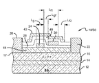
- チャネルを有する活性領域と、
前記活性領域と接触して形成されたソース電極およびドレイン電極と、
前記ソース電極とドレイン電極との間に、前記活性領域上に形成されたゲートと、
複数のスペーサ層と、
複数のフィールドプレートと
を備え、前記スペーサ層のうちの第1のスペーサ層は、前記ゲートと前記ドレイン電極およびソース電極との間の前記活性領域の表面の少なくとも一部の上にあり、前記フィールドプレートのうちの第1のフィールドプレートは、前記スペーサ層のうちの前記第1のスペーサ層上にあり、前記スペーサ層とフィールドプレートのうちの残りのスペーサ層とフィールドプレートは、前記スペーサ層のうちの前記第1のスペーサ層と前記フィールドプレートのうちの前記第1のフィールドプレートの上に交互に配置され、前記フィールドプレートのうちの最上部のフィールドプレートは、前記ソース電極に電気的に接続され、前記フィールドプレートのうちの前記最上部のフィールドプレートの下の前記フィールドプレートのそれぞれは、前記ゲートまたはソース電極に電気的に接続されていることを特徴とするトランジスタ。 - 前記第1のフィールドプレート上の前記フィールドプレートのそれぞれは、前記スペーサ層のうちの1つのスペーサ層によって下のフィールドプレートから分離されていることを特徴とする請求項1に記載のトランジスタ。
- 前記フィールドプレートのそれぞれは、少なくとも1つの電気的に接続する導電性経路によって前記ソース電極またはゲートに接続されていることを特徴とする請求項1に記載のトランジスタ。
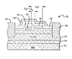
- 前記フィールドプレートのうちの前記第1のフィールドプレートは、前記ゲートのエッジから前記ドレイン電極に向かって延びる、前記スペーサ層のうちの前記第1のスペーサ層上に延びていることを特徴とする請求項1に記載のトランジスタ。
- 前記フィールドプレートのうちの第2のフィールドプレートは、前記フィールドプレートのうちの前記第1のフィールドプレートのエッジから前記ドレイン電極に向かって前記スペーサ層のうちの第2のスペーサ層上に延びていることを特徴とする請求項4に記載のトランジスタ。
- 前記スペーサ層のうちの前記第1のスペーサ層は、前記ゲートを少なくとも部分的に覆い、前記フィールドプレートのうちの前記第1のフィールドプレートは、前記ゲートと少なくとも部分的にオーバーラップし、前記ゲートのエッジから前記ドレイン電極に向かって前記スペーサ層のうちの前記第1のスペーサ層上で距離Lfだけ延びていることを特徴とする請求項1に記載のトランジスタ。
- 少なくとも1つの導電性経路をさらに備え、前記フィールドプレートのうちの少なくとも1つのフィールドプレートは、前記少なくとも1つの導電性経路によって前記ソース電極に電気的に接続され、前記経路のそれぞれは、前記活性領域の外側を走っていることを特徴とする請求項1に記載のトランジスタ。
- 少なくとも1つの導電性経路をさらに備え、前記スペーサ層のうちの1つのスペーサ層は、前記ゲート、ならびに前記ゲートとソース電極との間の前記活性領域の表面を覆い、前記フィールドプレートのうちの少なくとも1つのフィールドプレートは、前記少なくとも1つの導電性経路によって前記ソース電極に電気的に接続され、前記経路は、前記スペーサ層のうちの前記1つのスペーサ層上を走っていることを特徴とする請求項1に記載のトランジスタ。
- 高電子移動度トランジスタ(HEMT)を備えることを特徴とする請求項1に記載のトランジスタ。
- 電界効果トランジスタを備えることを特徴とする請求項1に記載のトランジスタ。
- 前記ゲートは、ガンマ形状をしていることを特徴とする請求項1に記載のトランジスタ。
- 前記ゲートは、前記活性領域中に少なくとも部分的にリセス化されていることを特徴とする請求項1に記載のトランジスタ。
- 前記フィールドプレートは、前記トランジスタ中のピーク動作電界を低減させることを特徴とする請求項1に記載のトランジスタ。
- ピーク動作電界の前記低減は、前記トランジスタの破壊電圧を増大させることを特徴とする請求項13に記載のトランジスタ。
- ピーク動作電界の前記低減は、前記トランジスタ中のトラッピングを低減させることを特徴とする請求項13に記載のトランジスタ。
- ピーク動作電界の前記低減は、前記トランジスタ中の漏れ電流を低減させることを特徴とする請求項13に記載のトランジスタ。
- 前記スペーサ層は、前記ゲートを完全には覆っておらず、前記第1のフィールドプレートは、前記ゲートと一体化して形成され、前記スペーサ層上で前記ドレイン電極に向かって距離Lfだけ延びていることを特徴とする請求項1に記載のトランジスタ。
- 前記スペーサ層は、誘電体材料を含むことを特徴とする請求項1に記載のトランジスタ。
- 前記スペーサ層のうちの少なくとも1つのスペーサ層は、エピタキシャル材料を含むことを特徴とする請求項1に記載のトランジスタ。
- 前記スペーサ層のうちの前記第1のスペーサ層は、エピタキシャル材料を含むことを特徴とする請求項1に記載のトランジスタ。
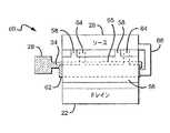
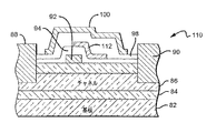
- チャネルを有する活性領域と、
前記活性領域と接触したソース電極およびドレイン電極と、
前記ソース電極とドレイン電極との間の、前記活性領域上のゲートと、
前記活性領域上に配置された複数のフィールドプレートと
を備え、フィールドプレートのそれぞれは、前記ゲートのエッジから前記ドレイン電極に向かって延びており、フィールドプレートのそれぞれは、前記活性領域から、また前記フィールドプレートのうちの他のフィールドプレートから分離され、前記フィールドプレートのうちの最上部のフィールドプレートは、前記ソース電極に電気的に接続され、前記フィールドプレートのうちの他のフィールドプレートのそれぞれは、前記ゲートまたは前記ソース電極に電気的に接続されていることを特徴とするトランジスタ。 - 前記活性領域上にやはり配置され、前記フィールドプレートの前記分離を実現する複数のスペーサ層をさらに備えることを特徴とする請求項21に記載のトランジスタ。
- 前記各スペーサ層は、前記フィールドプレートのそれぞれ1つのフィールドプレートと前記フィールドプレートの前記それぞれ1つのフィールドプレートの下の表面との間で挟まれることを特徴とする請求項22に記載のトランジスタ。
- 前記スペーサ層のうちの第1のスペーサ層は、前記フィールドプレートのうちの第1のフィールドプレートと前記活性領域の表面との間にあり、前記スペーサ層のうちの他のスペーサ層は、前記スペーサ層とフィールドプレートのうちの第1のスペーサ層とフィールドプレート上に交互に積み重なっていることを特徴とする請求項22に記載のトランジスタ。
- 前記フィールドプレートのそれぞれは、少なくとも1つの電気的に接続する導電性経路によって前記ソース電極またはゲートに電気的に接続されていることを特徴とする請求項21に記載のトランジスタ。
- 前記スペーサ層のうちの前記第1のスペーサ層は、前記ゲート、ならびに前記ゲートとドレイン電極との間の前記活性領域の表面の少なくとも一部分を少なくとも部分的に覆っており、前記フィールドプレートのうちの前記第1のフィールドプレートは、前記ゲートと少なくとも部分的にオーバーラップしており、前記ゲートのエッジから前記ドレイン電極に向かって前記スペーサ層のうちの前記第1のスペーサ層上で距離Lfだけ延びていることを特徴とする請求項21に記載のトランジスタ。
- 少なくとも1つの導電性経路をさらに備え、前記フィールドプレートのうちの少なくとも1つのフィールドプレートは、前記少なくとも1つの導電性経路によって前記ソース電極に電気的に接続され、前記経路のそれぞれは、前記スペーサ層の外側を走っていることを特徴とする請求項21に記載のトランジスタ。
- 少なくとも1つの導電性経路をさらに備え、前記スペーサ層のうちの1つのスペーサ層は、前記ゲート、ならびに前記ゲートとソース電極との間の前記活性領域の表面を覆っており、前記フィールドプレートのうちの少なくとも1つのフィールドプレートは、前記少なくとも1つの導電性経路によって前記ソース電極に電気的に接続され、前記経路は、前記スペーサ層のうちの前記1つのスペーサ層上を走っていることを特徴とする請求項21に記載のトランジスタ。
- 高電子移動度トランジスタ(HEMT)を備えることを特徴とする請求項21に記載のトランジスタ。
- 電界効果トランジスタを備えることを特徴とする請求項21に記載のトランジスタ。
- 前記ゲートは、ガンマ形状をしていることを特徴とする請求項21に記載のトランジスタ。
- 前記ゲートは、前記活性領域中に少なくとも部分的にリセス化されていることを特徴とする請求項21に記載のトランジスタ。
- 前記フィールドプレートは、前記トランジスタ中のピーク動作電界を低減させることを特徴とする請求項21に記載のトランジスタ。
Applications Claiming Priority (3)
| Application Number | Priority Date | Filing Date | Title |
|---|---|---|---|
| US57051804P | 2004-05-11 | 2004-05-11 | |
| US10/976,422 US7573078B2 (en) | 2004-05-11 | 2004-10-29 | Wide bandgap transistors with multiple field plates |
| PCT/US2005/012821 WO2005114743A2 (en) | 2004-05-11 | 2005-04-14 | Wide bandgap transistors with multiple field plates |
Related Child Applications (1)
| Application Number | Title | Priority Date | Filing Date |
|---|---|---|---|
| JP2013050780A Division JP5755671B2 (ja) | 2004-05-11 | 2013-03-13 | 複数のフィールドプレートを有するワイドバンドギャップトランジスタ |
Publications (2)
| Publication Number | Publication Date |
|---|---|
| JP2007537594A true JP2007537594A (ja) | 2007-12-20 |
| JP2007537594A5 JP2007537594A5 (ja) | 2008-04-03 |
Family
ID=34965673
Family Applications (2)
| Application Number | Title | Priority Date | Filing Date |
|---|---|---|---|
| JP2007513155A Pending JP2007537594A (ja) | 2004-05-11 | 2005-04-14 | 複数のフィールドプレートを有するワイドバンドギャップトランジスタ |
| JP2013050780A Active JP5755671B2 (ja) | 2004-05-11 | 2013-03-13 | 複数のフィールドプレートを有するワイドバンドギャップトランジスタ |
Family Applications After (1)
| Application Number | Title | Priority Date | Filing Date |
|---|---|---|---|
| JP2013050780A Active JP5755671B2 (ja) | 2004-05-11 | 2013-03-13 | 複数のフィールドプレートを有するワイドバンドギャップトランジスタ |
Country Status (8)
| Country | Link |
|---|---|
| US (2) | US7573078B2 (ja) |
| EP (2) | EP1751804B1 (ja) |
| JP (2) | JP2007537594A (ja) |
| KR (1) | KR101057439B1 (ja) |
| CN (1) | CN1950945B (ja) |
| CA (1) | CA2566361C (ja) |
| TW (1) | TW200607092A (ja) |
| WO (1) | WO2005114743A2 (ja) |
Cited By (13)
| Publication number | Priority date | Publication date | Assignee | Title |
|---|---|---|---|---|
| JP2008243943A (ja) * | 2007-03-26 | 2008-10-09 | Sanken Electric Co Ltd | 半導体装置およびその製造方法 |
| JP2009032724A (ja) * | 2007-07-24 | 2009-02-12 | Sony Corp | 電界効果型トランジスタ、及びそれを備えたパワーアンプモジュール及び移動体通信装置並びに電界効果型トランジスタの製造方法 |
| CN102201442A (zh) * | 2011-04-02 | 2011-09-28 | 中国科学院苏州纳米技术与纳米仿生研究所 | 基于沟道阵列结构的异质结场效应晶体管 |
| JP2011210752A (ja) * | 2010-03-26 | 2011-10-20 | Nec Corp | 半導体装置、電子装置、半導体装置の製造方法、および半導体装置の動作方法 |
| JP2012028423A (ja) * | 2010-07-20 | 2012-02-09 | Sumitomo Electric Device Innovations Inc | 半導体装置 |
| US8253169B2 (en) | 2008-09-09 | 2012-08-28 | Kabushiki Kaisha Toshiba | Semiconductor device and manufacturing method for semiconductor device |
| JP2013131758A (ja) * | 2011-12-21 | 2013-07-04 | Power Integrations Inc | 半導体装置 |
| JP2013175754A (ja) * | 2009-04-21 | 2013-09-05 | Infineon Technologies Austria Ag | 横型hemt |
| WO2014050054A1 (ja) * | 2012-09-28 | 2014-04-03 | パナソニック株式会社 | 半導体装置 |
| JP2018026431A (ja) * | 2016-08-09 | 2018-02-15 | 株式会社東芝 | 窒化物半導体装置 |
| JP2018157008A (ja) * | 2017-03-16 | 2018-10-04 | サンケン電気株式会社 | 半導体装置 |
| JP2020047741A (ja) * | 2018-09-18 | 2020-03-26 | 株式会社東芝 | 半導体装置 |
| JP2021108393A (ja) * | 2020-04-07 | 2021-07-29 | ローム株式会社 | 半導体装置 |
Families Citing this family (169)
| Publication number | Priority date | Publication date | Assignee | Title |
|---|---|---|---|---|
| CA2454269C (en) * | 2001-07-24 | 2015-07-07 | Primit Parikh | Insulating gate algan/gan hemt |
| EP1665358B1 (en) * | 2003-09-09 | 2020-07-01 | The Regents of The University of California | Fabrication of single or multiple gate field plates |
| US7501669B2 (en) | 2003-09-09 | 2009-03-10 | Cree, Inc. | Wide bandgap transistor devices with field plates |
| US7550783B2 (en) | 2004-05-11 | 2009-06-23 | Cree, Inc. | Wide bandgap HEMTs with source connected field plates |
| US7573078B2 (en) * | 2004-05-11 | 2009-08-11 | Cree, Inc. | Wide bandgap transistors with multiple field plates |
| US9773877B2 (en) * | 2004-05-13 | 2017-09-26 | Cree, Inc. | Wide bandgap field effect transistors with source connected field plates |
| TWI278090B (en) * | 2004-10-21 | 2007-04-01 | Int Rectifier Corp | Solderable top metal for SiC device |
| US7812441B2 (en) | 2004-10-21 | 2010-10-12 | Siliconix Technology C.V. | Schottky diode with improved surge capability |
| US9640649B2 (en) * | 2004-12-30 | 2017-05-02 | Infineon Technologies Americas Corp. | III-nitride power semiconductor with a field relaxation feature |
| US7834376B2 (en) | 2005-03-04 | 2010-11-16 | Siliconix Technology C. V. | Power semiconductor switch |
| US9419092B2 (en) * | 2005-03-04 | 2016-08-16 | Vishay-Siliconix | Termination for SiC trench devices |
| US11791385B2 (en) * | 2005-03-11 | 2023-10-17 | Wolfspeed, Inc. | Wide bandgap transistors with gate-source field plates |
| EP1901342A4 (en) * | 2005-06-10 | 2009-07-22 | Nec Corp | FIELD EFFECT TRANSISTOR |
| EP1901341A4 (en) * | 2005-06-10 | 2009-07-15 | Nec Corp | FIELD EFFECT TRANSISTOR |
| US7855401B2 (en) | 2005-06-29 | 2010-12-21 | Cree, Inc. | Passivation of wide band-gap based semiconductor devices with hydrogen-free sputtered nitrides |
| US7525122B2 (en) | 2005-06-29 | 2009-04-28 | Cree, Inc. | Passivation of wide band-gap based semiconductor devices with hydrogen-free sputtered nitrides |
| JP4751150B2 (ja) * | 2005-08-31 | 2011-08-17 | 株式会社東芝 | 窒化物系半導体装置 |
| EP2312634B1 (en) * | 2005-09-07 | 2019-12-25 | Cree, Inc. | Transistors with fluorine treatment |
| US8368165B2 (en) | 2005-10-20 | 2013-02-05 | Siliconix Technology C. V. | Silicon carbide Schottky diode |
| DE112007000092B4 (de) * | 2006-01-09 | 2014-07-24 | International Rectifier Corp. | Gruppe-III-Nitrid-Leistungshalbleiter mit einem Feld-Relaxations-Merkmal |
| EP1983563A4 (en) * | 2006-02-10 | 2009-07-29 | Nec Corp | SEMICONDUCTOR COMPONENT |
| US7388236B2 (en) * | 2006-03-29 | 2008-06-17 | Cree, Inc. | High efficiency and/or high power density wide bandgap transistors |
| JP2007273920A (ja) * | 2006-03-31 | 2007-10-18 | Eudyna Devices Inc | 半導体装置およびその製造方法 |
| JP2009545885A (ja) * | 2006-07-31 | 2009-12-24 | ヴィシェイ−シリコニックス | SiCショットキーダイオード用モリブデンバリア金属および製造方法 |
| KR100782430B1 (ko) * | 2006-09-22 | 2007-12-05 | 한국과학기술원 | 고전력을 위한 내부전계전극을 갖는 갈륨나이트라이드기반의 고전자 이동도 트랜지스터 구조 |
| KR100770132B1 (ko) | 2006-10-30 | 2007-10-24 | 페어차일드코리아반도체 주식회사 | 질화물계 반도체 소자 |
| EP1921669B1 (en) * | 2006-11-13 | 2015-09-02 | Cree, Inc. | GaN based HEMTs with buried field plates |
| US7692263B2 (en) * | 2006-11-21 | 2010-04-06 | Cree, Inc. | High voltage GaN transistors |
| US8878245B2 (en) | 2006-11-30 | 2014-11-04 | Cree, Inc. | Transistors and method for making ohmic contact to transistors |
| JP5512287B2 (ja) * | 2007-02-22 | 2014-06-04 | フォルシュングスフェアブント ベルリン エー ファウ | 半導体素子およびその製造方法 |
| KR100857683B1 (ko) | 2007-03-07 | 2008-09-08 | 페어차일드코리아반도체 주식회사 | 질화물 반도체 소자 및 그 제조방법 |
| US8212290B2 (en) | 2007-03-23 | 2012-07-03 | Cree, Inc. | High temperature performance capable gallium nitride transistor |
| US8174051B2 (en) * | 2007-06-26 | 2012-05-08 | International Rectifier Corporation | III-nitride power device |
| US7915643B2 (en) | 2007-09-17 | 2011-03-29 | Transphorm Inc. | Enhancement mode gallium nitride power devices |
| US7800132B2 (en) * | 2007-10-25 | 2010-09-21 | Northrop Grumman Systems Corporation | High electron mobility transistor semiconductor device having field mitigating plate and fabrication method thereof |
| KR100985470B1 (ko) * | 2008-04-18 | 2010-10-06 | 고려대학교 산학협력단 | 고 전자 이동도 트랜지스터 및 그 제조방법 |
| US8519438B2 (en) | 2008-04-23 | 2013-08-27 | Transphorm Inc. | Enhancement mode III-N HEMTs |
| US7985986B2 (en) | 2008-07-31 | 2011-07-26 | Cree, Inc. | Normally-off semiconductor devices |
| US8289065B2 (en) | 2008-09-23 | 2012-10-16 | Transphorm Inc. | Inductive load power switching circuits |
| US7898004B2 (en) | 2008-12-10 | 2011-03-01 | Transphorm Inc. | Semiconductor heterostructure diodes |
| JP2010219117A (ja) * | 2009-03-13 | 2010-09-30 | Toshiba Corp | 半導体装置 |
| US8754496B2 (en) * | 2009-04-14 | 2014-06-17 | Triquint Semiconductor, Inc. | Field effect transistor having a plurality of field plates |
| US8008977B2 (en) * | 2009-04-14 | 2011-08-30 | Triquint Semiconductor, Inc. | Field-plated transistor including feedback resistor |
| US8742459B2 (en) | 2009-05-14 | 2014-06-03 | Transphorm Inc. | High voltage III-nitride semiconductor devices |
| JP5595685B2 (ja) * | 2009-07-28 | 2014-09-24 | パナソニック株式会社 | 半導体装置 |
| US8390000B2 (en) | 2009-08-28 | 2013-03-05 | Transphorm Inc. | Semiconductor devices with field plates |
| KR101632314B1 (ko) * | 2009-09-11 | 2016-06-22 | 삼성전자주식회사 | 전계 효과형 반도체 소자 및 그 제조 방법 |
| US7999287B2 (en) | 2009-10-26 | 2011-08-16 | Infineon Technologies Austria Ag | Lateral HEMT and method for the production of a lateral HEMT |
| US8592865B1 (en) | 2009-10-29 | 2013-11-26 | Hrl Laboratories, Llc | Overvoltage tolerant HFETs |
| US8338860B2 (en) * | 2009-10-30 | 2012-12-25 | Alpha And Omega Semiconductor Incorporated | Normally off gallium nitride field effect transistors (FET) |
| CN101707208A (zh) * | 2009-11-03 | 2010-05-12 | 苏州远创达科技有限公司 | 多重场板ldmos器件及其加工方法 |
| US8389977B2 (en) | 2009-12-10 | 2013-03-05 | Transphorm Inc. | Reverse side engineered III-nitride devices |
| KR101226955B1 (ko) * | 2009-12-11 | 2013-01-28 | 한국전자통신연구원 | 전계 효과 트랜지스터의 제조방법 |
| US8829999B2 (en) | 2010-05-20 | 2014-09-09 | Cree, Inc. | Low noise amplifiers including group III nitride based high electron mobility transistors |
| JP2011249728A (ja) * | 2010-05-31 | 2011-12-08 | Toshiba Corp | 半導体装置および半導体装置の製造方法 |
| JP2012109492A (ja) * | 2010-11-19 | 2012-06-07 | Sanken Electric Co Ltd | 化合物半導体装置 |
| JP5707903B2 (ja) * | 2010-12-02 | 2015-04-30 | 富士通株式会社 | 化合物半導体装置及びその製造方法 |
| JP5724339B2 (ja) * | 2010-12-03 | 2015-05-27 | 富士通株式会社 | 化合物半導体装置及びその製造方法 |
| KR101583094B1 (ko) | 2010-12-14 | 2016-01-07 | 한국전자통신연구원 | 반도체 소자 및 이의 제조방법 |
| US8742460B2 (en) | 2010-12-15 | 2014-06-03 | Transphorm Inc. | Transistors with isolation regions |
| KR101775560B1 (ko) | 2010-12-17 | 2017-09-07 | 한국전자통신연구원 | 전계효과 트랜지스터 및 그 제조 방법 |
| US8643062B2 (en) | 2011-02-02 | 2014-02-04 | Transphorm Inc. | III-N device structures and methods |
| JP5776217B2 (ja) * | 2011-02-24 | 2015-09-09 | 富士通株式会社 | 化合物半導体装置 |
| US8716141B2 (en) | 2011-03-04 | 2014-05-06 | Transphorm Inc. | Electrode configurations for semiconductor devices |
| US8772842B2 (en) | 2011-03-04 | 2014-07-08 | Transphorm, Inc. | Semiconductor diodes with low reverse bias currents |
| KR20120120826A (ko) | 2011-04-25 | 2012-11-02 | 삼성전기주식회사 | 질화물 반도체 소자 및 그 제조방법 |
| US8901604B2 (en) | 2011-09-06 | 2014-12-02 | Transphorm Inc. | Semiconductor devices with guard rings |
| JP5979836B2 (ja) | 2011-09-09 | 2016-08-31 | ルネサスエレクトロニクス株式会社 | 半導体装置および半導体装置の製造方法 |
| US9257547B2 (en) | 2011-09-13 | 2016-02-09 | Transphorm Inc. | III-N device structures having a non-insulating substrate |
| US8772833B2 (en) * | 2011-09-21 | 2014-07-08 | Electronics And Telecommunications Research Institute | Power semiconductor device and fabrication method thereof |
| JP5908692B2 (ja) * | 2011-09-29 | 2016-04-26 | トランスフォーム・ジャパン株式会社 | 化合物半導体装置及びその製造方法 |
| JP6014984B2 (ja) * | 2011-09-29 | 2016-10-26 | 富士通株式会社 | 半導体装置及びその製造方法 |
| US8598937B2 (en) | 2011-10-07 | 2013-12-03 | Transphorm Inc. | High power semiconductor electronic components with increased reliability |
| JP5864214B2 (ja) * | 2011-10-31 | 2016-02-17 | 株式会社日立製作所 | 半導体装置 |
| CN102420247B (zh) * | 2011-11-18 | 2013-10-30 | 中国科学院苏州纳米技术与纳米仿生研究所 | Ⅲ族氮化物hemt器件 |
| US9070756B2 (en) * | 2011-11-18 | 2015-06-30 | Suzhou Institute Of Nano-Tech And Nano-Bionics Of Chinese Academy Of Sciences | Group III nitride high electron mobility transistor (HEMT) device |
| CN102427086B (zh) * | 2011-11-18 | 2013-09-25 | 中国科学院苏州纳米技术与纳米仿生研究所 | Ⅲ族氮化物增强型mishemt器件 |
| CN102403349B (zh) * | 2011-11-18 | 2013-09-25 | 中国科学院苏州纳米技术与纳米仿生研究所 | Ⅲ族氮化物mishemt器件 |
| US8530978B1 (en) | 2011-12-06 | 2013-09-10 | Hrl Laboratories, Llc | High current high voltage GaN field effect transistors and method of fabricating same |
| US9165766B2 (en) | 2012-02-03 | 2015-10-20 | Transphorm Inc. | Buffer layer structures suited for III-nitride devices with foreign substrates |
| JP5895666B2 (ja) * | 2012-03-30 | 2016-03-30 | 富士通株式会社 | 化合物半導体装置及びその製造方法 |
| US9093366B2 (en) | 2012-04-09 | 2015-07-28 | Transphorm Inc. | N-polar III-nitride transistors |
| US9443941B2 (en) * | 2012-06-04 | 2016-09-13 | Infineon Technologies Austria Ag | Compound semiconductor transistor with self aligned gate |
| US8962433B2 (en) * | 2012-06-12 | 2015-02-24 | United Microelectronics Corp. | MOS transistor process |
| US9184275B2 (en) | 2012-06-27 | 2015-11-10 | Transphorm Inc. | Semiconductor devices with integrated hole collectors |
| US9245879B2 (en) * | 2012-06-29 | 2016-01-26 | Power Integrations, Inc. | Static discharge system |
| JP2014017423A (ja) * | 2012-07-10 | 2014-01-30 | Fujitsu Ltd | 化合物半導体装置及びその製造方法 |
| US9024324B2 (en) | 2012-09-05 | 2015-05-05 | Freescale Semiconductor, Inc. | GaN dual field plate device with single field plate metal |
| JP2014072379A (ja) * | 2012-09-28 | 2014-04-21 | Fujitsu Ltd | 化合物半導体装置及びその製造方法 |
| US8994073B2 (en) | 2012-10-04 | 2015-03-31 | Cree, Inc. | Hydrogen mitigation schemes in the passivation of advanced devices |
| US9991399B2 (en) | 2012-10-04 | 2018-06-05 | Cree, Inc. | Passivation structure for semiconductor devices |
| US9812338B2 (en) | 2013-03-14 | 2017-11-07 | Cree, Inc. | Encapsulation of advanced devices using novel PECVD and ALD schemes |
| US9799762B2 (en) * | 2012-12-03 | 2017-10-24 | Infineon Technologies Ag | Semiconductor device and method of manufacturing a semiconductor device |
| KR101923959B1 (ko) | 2012-12-11 | 2018-12-03 | 한국전자통신연구원 | 트랜지스터 및 그 제조 방법 |
| KR101923972B1 (ko) | 2012-12-18 | 2018-11-30 | 한국전자통신연구원 | 트랜지스터 및 그 제조 방법 |
| JP6522521B2 (ja) | 2013-02-15 | 2019-05-29 | トランスフォーム インコーポレーテッド | 半導体デバイスの電極及びその製造方法 |
| US9087718B2 (en) | 2013-03-13 | 2015-07-21 | Transphorm Inc. | Enhancement-mode III-nitride devices |
| US9048184B2 (en) * | 2013-03-15 | 2015-06-02 | Northrop Grumman Systems Corporation | Method of forming a gate contact |
| US9245992B2 (en) | 2013-03-15 | 2016-01-26 | Transphorm Inc. | Carbon doping semiconductor devices |
| US9142626B1 (en) | 2013-04-23 | 2015-09-22 | Hrl Laboratories, Llc | Stepped field plate wide bandgap field-effect transistor and method |
| US9755059B2 (en) | 2013-06-09 | 2017-09-05 | Cree, Inc. | Cascode structures with GaN cap layers |
| US9847411B2 (en) | 2013-06-09 | 2017-12-19 | Cree, Inc. | Recessed field plate transistor structures |
| US9679981B2 (en) | 2013-06-09 | 2017-06-13 | Cree, Inc. | Cascode structures for GaN HEMTs |
| US9407214B2 (en) | 2013-06-28 | 2016-08-02 | Cree, Inc. | MMIC power amplifier |
| US9443938B2 (en) | 2013-07-19 | 2016-09-13 | Transphorm Inc. | III-nitride transistor including a p-type depleting layer |
| US9287404B2 (en) | 2013-10-02 | 2016-03-15 | Infineon Technologies Austria Ag | Semiconductor device and method of manufacturing a semiconductor device with lateral FET cells and field plates |
| US9306058B2 (en) | 2013-10-02 | 2016-04-05 | Infineon Technologies Ag | Integrated circuit and method of manufacturing an integrated circuit |
| US9401399B2 (en) | 2013-10-15 | 2016-07-26 | Infineon Technologies Ag | Semiconductor device |
| KR102100928B1 (ko) * | 2013-10-17 | 2020-05-15 | 삼성전자주식회사 | 고전자 이동도 트랜지스터 |
| CN103779208B (zh) * | 2014-01-02 | 2016-04-06 | 中国电子科技集团公司第五十五研究所 | 一种低噪声GaN HEMT器件的制备方法 |
| JP2015177016A (ja) * | 2014-03-14 | 2015-10-05 | 株式会社東芝 | 半導体装置 |
| DE102014103540B4 (de) * | 2014-03-14 | 2020-02-20 | Infineon Technologies Austria Ag | Halbleiterbauelement und integrierte schaltung |
| US8980759B1 (en) | 2014-05-22 | 2015-03-17 | Hrl Laboratories, Llc | Method of fabricating slanted field-plate GaN heterojunction field-effect transistor |
| US10276712B2 (en) | 2014-05-29 | 2019-04-30 | Hrl Laboratories, Llc | III-nitride field-effect transistor with dual gates |
| KR102135163B1 (ko) | 2014-06-26 | 2020-07-20 | 한국전자통신연구원 | 반도체 소자 및 그 제작 방법 |
| US9318593B2 (en) | 2014-07-21 | 2016-04-19 | Transphorm Inc. | Forming enhancement mode III-nitride devices |
| US9620598B2 (en) | 2014-08-05 | 2017-04-11 | Semiconductor Components Industries, Llc | Electronic device including a channel layer including gallium nitride |
| US9640623B2 (en) | 2014-10-17 | 2017-05-02 | Cree, Inc. | Semiconductor device with improved field plate |
| US9608078B2 (en) | 2014-10-17 | 2017-03-28 | Cree, Inc. | Semiconductor device with improved field plate |
| US10062756B2 (en) | 2014-10-30 | 2018-08-28 | Semiconductor Components Industries, Llc | Semiconductor structure including a doped buffer layer and a channel layer and a process of forming the same |
| CN104465747B (zh) * | 2014-11-18 | 2017-03-29 | 西安电子科技大学 | T形源‑漏复合场板功率器件 |
| CN104393041B (zh) * | 2014-11-18 | 2017-04-19 | 西安电子科技大学 | T形栅场板高电子迁移率晶体管及其制作方法 |
| CN104393043B (zh) * | 2014-11-18 | 2017-04-19 | 西安电子科技大学 | 氮化镓基直角漏场板高电子迁移率晶体管 |
| CN104409493B (zh) * | 2014-11-18 | 2017-03-29 | 西安电子科技大学 | 基于t形栅‑漏复合场板的异质结器件及其制作方法 |
| US9536967B2 (en) | 2014-12-16 | 2017-01-03 | Transphorm Inc. | Recessed ohmic contacts in a III-N device |
| US9536966B2 (en) | 2014-12-16 | 2017-01-03 | Transphorm Inc. | Gate structures for III-N devices |
| TWI557919B (zh) * | 2015-03-09 | 2016-11-11 | 世界先進積體電路股份有限公司 | 半導體裝置及其製造方法 |
| US9818861B2 (en) | 2015-04-24 | 2017-11-14 | Vanguard International Semiconductor Corporation | Semiconductor device and method for forming the same |
| TWI626742B (zh) | 2015-06-18 | 2018-06-11 | 台達電子工業股份有限公司 | 半導體裝置 |
| CN106328699B (zh) * | 2015-07-03 | 2020-04-14 | 台达电子工业股份有限公司 | 半导体装置 |
| TWI617027B (zh) * | 2015-07-03 | 2018-03-01 | 台達電子工業股份有限公司 | 半導體裝置 |
| US9812532B1 (en) | 2015-08-28 | 2017-11-07 | Hrl Laboratories, Llc | III-nitride P-channel transistor |
| US9755027B2 (en) | 2015-09-15 | 2017-09-05 | Electronics And Telecommunications Research Institute | Electronical device |
| US10056478B2 (en) * | 2015-11-06 | 2018-08-21 | Taiwan Semiconductor Manufacturing Company Ltd. | High-electron-mobility transistor and manufacturing method thereof |
| CN108292678B (zh) | 2015-11-19 | 2021-07-06 | Hrl实验室有限责任公司 | 具有双栅极的iii族氮化物场效应晶体管 |
| US11322599B2 (en) | 2016-01-15 | 2022-05-03 | Transphorm Technology, Inc. | Enhancement mode III-nitride devices having an Al1-xSixO gate insulator |
| KR102208076B1 (ko) * | 2016-02-12 | 2021-01-28 | 한국전자통신연구원 | 고전자 이동도 트랜지스터 및 그 제조방법 |
| US10396166B2 (en) | 2016-03-11 | 2019-08-27 | Mediatek Inc. | Semiconductor device capable of high-voltage operation |
| US10199496B2 (en) | 2016-03-11 | 2019-02-05 | Mediatek Inc. | Semiconductor device capable of high-voltage operation |
| US10418480B2 (en) * | 2016-03-11 | 2019-09-17 | Mediatek Inc. | Semiconductor device capable of high-voltage operation |
| US10224401B2 (en) | 2016-05-31 | 2019-03-05 | Transphorm Inc. | III-nitride devices including a graded depleting layer |
| CN106298882B (zh) * | 2016-08-04 | 2019-10-08 | 苏州能讯高能半导体有限公司 | 高电子迁移率晶体管器件及其制造方法 |
| TWI607565B (zh) | 2016-12-20 | 2017-12-01 | 新唐科技股份有限公司 | 半導體基底以及半導體元件 |
| CN107170799B (zh) * | 2017-03-29 | 2019-10-11 | 西安电子科技大学 | 浮空栅-漏复合场板垂直型电力电子器件 |
| JP6874928B2 (ja) * | 2017-10-24 | 2021-05-19 | 住友電工デバイス・イノベーション株式会社 | 半導体装置 |
| US10700188B2 (en) * | 2017-11-02 | 2020-06-30 | Rohm Co., Ltd. | Group III nitride semiconductor device with first and second conductive layers |
| KR20190090231A (ko) | 2018-01-24 | 2019-08-01 | (주)웨이비스 | 크랙이 없는 고신뢰성 필드 플레이트를 포함하는 고전자이동도 트랜지스터 및 이의 제조방법 |
| US11121245B2 (en) | 2019-02-22 | 2021-09-14 | Efficient Power Conversion Corporation | Field plate structures with patterned surface passivation layers and methods for manufacturing thereof |
| JP2020150193A (ja) | 2019-03-15 | 2020-09-17 | 株式会社東芝 | 半導体装置 |
| TWI706564B (zh) * | 2019-08-08 | 2020-10-01 | 世界先進積體電路股份有限公司 | 半導體結構及其形成方法 |
| US11114532B2 (en) * | 2019-11-20 | 2021-09-07 | Vanguard International Semiconductor Corporation | Semiconductor structures and methods of forming the same |
| CN113675262B (zh) * | 2020-05-14 | 2023-12-05 | 苏州华太电子技术股份有限公司 | 应用于半导体器件的场板结构及其制作方法和应用 |
| US11316019B2 (en) * | 2020-07-29 | 2022-04-26 | Globalfoundries U.S. Inc. | Symmetric arrangement of field plates in semiconductor devices |
| US11749726B2 (en) | 2020-10-27 | 2023-09-05 | Wolfspeed, Inc. | Field effect transistor with source-connected field plate |
| US11502178B2 (en) | 2020-10-27 | 2022-11-15 | Wolfspeed, Inc. | Field effect transistor with at least partially recessed field plate |
| US11658234B2 (en) | 2020-10-27 | 2023-05-23 | Wolfspeed, Inc. | Field effect transistor with enhanced reliability |
| WO2022116915A1 (zh) * | 2020-12-01 | 2022-06-09 | 深圳市晶相技术有限公司 | 一种半导体器件及其应用与制造方法 |
| US11923424B2 (en) * | 2020-12-31 | 2024-03-05 | Nxp B.V. | Semiconductor device with conductive elements formed over dielectric layers and method of fabrication therefor |
| CN112750898A (zh) * | 2021-01-07 | 2021-05-04 | 王琮 | 基于氮化镓的半导体功率器件及其制造方法 |
| CN113016074B (zh) | 2021-02-19 | 2022-08-12 | 英诺赛科(苏州)科技有限公司 | 半导体器件 |
| KR20240005063A (ko) * | 2021-05-20 | 2024-01-11 | 울프스피드, 인크. | 소스 접속된 필드 플레이트를 갖는 전계 효과 트랜지스터 |
| US11869964B2 (en) | 2021-05-20 | 2024-01-09 | Wolfspeed, Inc. | Field effect transistors with modified access regions |
| US20220376060A1 (en) * | 2021-05-20 | 2022-11-24 | Nxp Usa, Inc. | Semiconductor device with conductive element formed over dielectric layers and method of fabrication therefor |
| CN113725286A (zh) * | 2021-07-21 | 2021-11-30 | 中山市华南理工大学现代产业技术研究院 | 一种高耐压的GaN基HEMT器件及其制备方法 |
| US11621672B2 (en) | 2021-08-05 | 2023-04-04 | Wolfspeed, Inc. | Compensation of trapping in field effect transistors |
| CN113436975B (zh) * | 2021-08-27 | 2021-12-14 | 深圳市时代速信科技有限公司 | 一种半导体器件及制备方法 |
| US11894430B2 (en) * | 2021-09-16 | 2024-02-06 | Vanguard International Semiconductor Corporation | Semiconductor structure |
| US20230352476A1 (en) * | 2021-10-27 | 2023-11-02 | Innoscience (Suzhou) Technology Co., Ltd. | Nitride-based semiconductor device and method for manufacturing the same |
| US20230207641A1 (en) * | 2021-12-29 | 2023-06-29 | Nxp Usa, Inc. | Transistor with aligned field plate and method of fabrication therefor |
Citations (5)
| Publication number | Priority date | Publication date | Assignee | Title |
|---|---|---|---|---|
| JPH06349859A (ja) * | 1993-06-10 | 1994-12-22 | Rohm Co Ltd | 電界効果トランジスタ |
| JPH11274174A (ja) * | 1998-03-20 | 1999-10-08 | Nec Corp | 電界効果トランジスタの製造方法 |
| JP2000100831A (ja) * | 1998-09-22 | 2000-04-07 | Nec Corp | 電界効果型トランジスタ |
| JP2002270830A (ja) * | 2001-03-12 | 2002-09-20 | Fuji Electric Co Ltd | 半導体装置 |
| WO2003032397A2 (en) * | 2001-07-24 | 2003-04-17 | Cree, Inc. | INSULTING GATE AlGaN/GaN HEMT |
Family Cites Families (107)
| Publication number | Priority date | Publication date | Assignee | Title |
|---|---|---|---|---|
| US227211A (en) * | 1880-05-04 | James bowees | ||
| US5187552A (en) | 1979-03-28 | 1993-02-16 | Hendrickson Thomas E | Shielded field-effect transistor devices |
| US4290077A (en) | 1979-05-30 | 1981-09-15 | Xerox Corporation | High voltage MOSFET with inter-device isolation structure |
| US4947232A (en) | 1980-03-22 | 1990-08-07 | Sharp Kabushiki Kaisha | High voltage MOS transistor |
| JPS56169368A (en) | 1980-05-30 | 1981-12-26 | Sharp Corp | High withstand voltage mos field effect semiconductor device |
| NL8103218A (nl) | 1981-07-06 | 1983-02-01 | Philips Nv | Veldeffekttransistor met geisoleerde stuurelektrode. |
| US4551905A (en) | 1982-12-09 | 1985-11-12 | Cornell Research Foundation, Inc. | Fabrication of metal lines for semiconductor devices |
| JPS62237763A (ja) | 1986-04-08 | 1987-10-17 | Agency Of Ind Science & Technol | 半導体装置の製造方法 |
| US5196359A (en) | 1988-06-30 | 1993-03-23 | Texas Instruments Incorporated | Method of forming heterostructure field effect transistor |
| JPH0335536A (ja) * | 1989-06-30 | 1991-02-15 | Fujitsu Ltd | 電界効果型半導体装置 |
| US5053348A (en) | 1989-12-01 | 1991-10-01 | Hughes Aircraft Company | Fabrication of self-aligned, t-gate hemt |
| US5290393A (en) | 1991-01-31 | 1994-03-01 | Nichia Kagaku Kogyo K.K. | Crystal growth method for gallium nitride-based compound semiconductor |
| EP0576566B1 (en) | 1991-03-18 | 1999-05-26 | Trustees Of Boston University | A method for the preparation and doping of highly insulating monocrystalline gallium nitride thin films |
| US5192987A (en) | 1991-05-17 | 1993-03-09 | Apa Optics, Inc. | High electron mobility transistor with GaN/Alx Ga1-x N heterojunctions |
| JPH0521793A (ja) | 1991-07-09 | 1993-01-29 | Mitsubishi Electric Corp | 半導体装置及びその製造方法 |
| JPH0661266A (ja) | 1992-08-06 | 1994-03-04 | Mitsubishi Electric Corp | 半導体装置とその製造方法 |
| JPH06224225A (ja) | 1993-01-27 | 1994-08-12 | Fujitsu Ltd | 電界効果半導体装置 |
| JPH06267991A (ja) | 1993-03-12 | 1994-09-22 | Hitachi Ltd | 半導体装置およびその製造方法 |
| US5393993A (en) | 1993-12-13 | 1995-02-28 | Cree Research, Inc. | Buffer structure between silicon carbide and gallium nitride and resulting semiconductor devices |
| JP2658860B2 (ja) | 1993-12-20 | 1997-09-30 | 日本電気株式会社 | 半導体装置およびその製造方法 |
| US5523589A (en) | 1994-09-20 | 1996-06-04 | Cree Research, Inc. | Vertical geometry light emitting diode with group III nitride active layer and extended lifetime |
| US5739554A (en) | 1995-05-08 | 1998-04-14 | Cree Research, Inc. | Double heterojunction light emitting diode with gallium nitride active layer |
| US6002148A (en) | 1995-06-30 | 1999-12-14 | Motorola, Inc. | Silicon carbide transistor and method |
| US5569937A (en) | 1995-08-28 | 1996-10-29 | Motorola | High breakdown voltage silicon carbide transistor |
| US5959307A (en) | 1995-11-06 | 1999-09-28 | Nichia Chemical Industries Ltd. | Nitride semiconductor device |
| KR0167273B1 (ko) | 1995-12-02 | 1998-12-15 | 문정환 | 고전압 모스전계효과트렌지스터의 구조 및 그 제조방법 |
| US6724040B2 (en) * | 1996-01-22 | 2004-04-20 | Fuji Electric Co., Ltd. | Semiconductor device |
| TW360982B (en) | 1996-01-26 | 1999-06-11 | Matsushita Electric Works Ltd | Thin film transistor of silicon-on-insulator type |
| JPH09232827A (ja) | 1996-02-21 | 1997-09-05 | Oki Electric Ind Co Ltd | 半導体装置及び送受信切り替え型アンテナスイッチ回路 |
| US5652179A (en) * | 1996-04-24 | 1997-07-29 | Watkins-Johnson Company | Method of fabricating sub-micron gate electrode by angle and direct evaporation |
| US5710455A (en) * | 1996-07-29 | 1998-01-20 | Motorola | Lateral MOSFET with modified field plates and damage areas |
| US5929467A (en) | 1996-12-04 | 1999-07-27 | Sony Corporation | Field effect transistor with nitride compound |
| JP3958404B2 (ja) | 1997-06-06 | 2007-08-15 | 三菱電機株式会社 | 横型高耐圧素子を有する半導体装置 |
| TW334632B (en) | 1997-07-24 | 1998-06-21 | Mitsubishi Electric Corp | Field effective semiconductor |
| JP3457511B2 (ja) | 1997-07-30 | 2003-10-20 | 株式会社東芝 | 半導体装置及びその製造方法 |
| US5898198A (en) | 1997-08-04 | 1999-04-27 | Spectrian | RF power device having voltage controlled linearity |
| US6346451B1 (en) * | 1997-12-24 | 2002-02-12 | Philips Electronics North America Corporation | Laterial thin-film silicon-on-insulator (SOI) device having a gate electrode and a field plate electrode |
| DE19800647C1 (de) | 1998-01-09 | 1999-05-27 | Siemens Ag | SOI-Hochspannungsschalter |
| US6316793B1 (en) | 1998-06-12 | 2001-11-13 | Cree, Inc. | Nitride based transistors on semi-insulating silicon carbide substrates |
| JP3111985B2 (ja) | 1998-06-16 | 2000-11-27 | 日本電気株式会社 | 電界効果型トランジスタ |
| JP2000082671A (ja) * | 1998-06-26 | 2000-03-21 | Sony Corp | 窒化物系iii−v族化合物半導体装置とその製造方法 |
| US6621121B2 (en) | 1998-10-26 | 2003-09-16 | Silicon Semiconductor Corporation | Vertical MOSFETs having trench-based gate electrodes within deeper trench-based source electrodes |
| JP2000164926A (ja) | 1998-11-24 | 2000-06-16 | Sony Corp | 化合物半導体の選択エッチング方法、窒化物系化合物半導体の選択エッチング方法、半導体装置および半導体装置の製造方法 |
| US6495409B1 (en) | 1999-01-26 | 2002-12-17 | Agere Systems Inc. | MOS transistor having aluminum nitride gate structure and method of manufacturing same |
| JP3429700B2 (ja) | 1999-03-19 | 2003-07-22 | 富士通カンタムデバイス株式会社 | 高電子移動度トランジスタ |
| US6127703A (en) * | 1999-08-31 | 2000-10-03 | Philips Electronics North America Corporation | Lateral thin-film silicon-on-insulator (SOI) PMOS device having a drain extension region |
| JP3371871B2 (ja) | 1999-11-16 | 2003-01-27 | 日本電気株式会社 | 半導体装置の製造方法 |
| US6639255B2 (en) | 1999-12-08 | 2003-10-28 | Matsushita Electric Industrial Co., Ltd. | GaN-based HFET having a surface-leakage reducing cap layer |
| US6586781B2 (en) | 2000-02-04 | 2003-07-01 | Cree Lighting Company | Group III nitride based FETs and HEMTs with reduced trapping and method for producing the same |
| US6686616B1 (en) | 2000-05-10 | 2004-02-03 | Cree, Inc. | Silicon carbide metal-semiconductor field effect transistors |
| WO2001087545A1 (en) * | 2000-05-16 | 2001-11-22 | Stanley Fastening Systems, L.P. | Fastener driving system and magazine assembly therefor |
| JP4186032B2 (ja) | 2000-06-29 | 2008-11-26 | 日本電気株式会社 | 半導体装置 |
| TWI257179B (en) | 2000-07-17 | 2006-06-21 | Fujitsu Quantum Devices Ltd | High-speed compound semiconductor device operable at large output power with minimum leakage current |
| JP4198339B2 (ja) * | 2000-07-17 | 2008-12-17 | ユーディナデバイス株式会社 | 化合物半導体装置 |
| US6624488B1 (en) * | 2000-08-07 | 2003-09-23 | Advanced Micro Devices, Inc. | Epitaxial silicon growth and usage of epitaxial gate insulator for low power, high performance devices |
| US6690042B2 (en) | 2000-09-27 | 2004-02-10 | Sensor Electronic Technology, Inc. | Metal oxide semiconductor heterostructure field effect transistor |
| US6891235B1 (en) | 2000-11-15 | 2005-05-10 | International Business Machines Corporation | FET with T-shaped gate |
| US6548333B2 (en) | 2000-12-01 | 2003-04-15 | Cree, Inc. | Aluminum gallium nitride/gallium nitride high electron mobility transistors having a gate contact on a gallium nitride based cap segment |
| US6791119B2 (en) | 2001-02-01 | 2004-09-14 | Cree, Inc. | Light emitting diodes including modifications for light extraction |
| US6468878B1 (en) | 2001-02-27 | 2002-10-22 | Koninklijke Philips Electronics N.V. | SOI LDMOS structure with improved switching characteristics |
| JP5020436B2 (ja) * | 2001-03-09 | 2012-09-05 | 新日本製鐵株式会社 | 電界効果トランジスタ |
| GB0107408D0 (en) | 2001-03-23 | 2001-05-16 | Koninkl Philips Electronics Nv | Field effect transistor structure and method of manufacture |
| JP4220683B2 (ja) | 2001-03-27 | 2009-02-04 | パナソニック株式会社 | 半導体装置 |
| US6849882B2 (en) | 2001-05-11 | 2005-02-01 | Cree Inc. | Group-III nitride based high electron mobility transistor (HEMT) with barrier/spacer layer |
| JP3744381B2 (ja) * | 2001-05-17 | 2006-02-08 | 日本電気株式会社 | 電界効果型トランジスタ |
| US6475857B1 (en) | 2001-06-21 | 2002-11-05 | Samsung Electronics Co., Ltd. | Method of making a scalable two transistor memory device |
| GB0122122D0 (en) | 2001-09-13 | 2001-10-31 | Koninkl Philips Electronics Nv | Trench-gate semiconductor devices and their manufacture |
| JP2003174039A (ja) | 2001-09-27 | 2003-06-20 | Murata Mfg Co Ltd | ヘテロ接合電界効果トランジスタ |
| US6906350B2 (en) | 2001-10-24 | 2005-06-14 | Cree, Inc. | Delta doped silicon carbide metal-semiconductor field effect transistors having a gate disposed in a double recess structure |
| AU2002339582A1 (en) | 2001-11-01 | 2003-05-12 | Koninklijke Philips Electronics N.V. | Lateral soi field-effect transistor |
| KR100445904B1 (ko) | 2001-12-12 | 2004-08-25 | 한국전자통신연구원 | 소스 필드 플레이트를 갖는 드레인 확장형 모스 전계 효과트랜지스터 및그 제조방법 |
| KR100438895B1 (ko) | 2001-12-28 | 2004-07-02 | 한국전자통신연구원 | 고전자 이동도 트랜지스터 전력 소자 및 그 제조 방법 |
| JP2003203930A (ja) | 2002-01-08 | 2003-07-18 | Nec Compound Semiconductor Devices Ltd | ショットキーゲート電界効果型トランジスタ |
| JP2003203923A (ja) | 2002-01-10 | 2003-07-18 | Mitsubishi Electric Corp | 半導体装置およびその製造方法 |
| GB0202437D0 (en) | 2002-02-02 | 2002-03-20 | Koninkl Philips Electronics Nv | Cellular mosfet devices and their manufacture |
| DE10206739C1 (de) | 2002-02-18 | 2003-08-21 | Infineon Technologies Ag | Transistorbauelement |
| JP3908572B2 (ja) | 2002-03-18 | 2007-04-25 | 株式会社東芝 | 半導体素子 |
| JP3705431B2 (ja) | 2002-03-28 | 2005-10-12 | ユーディナデバイス株式会社 | 半導体装置及びその製造方法 |
| JP3723780B2 (ja) | 2002-03-29 | 2005-12-07 | ユーディナデバイス株式会社 | 半導体装置及びその製造方法 |
| US6559513B1 (en) | 2002-04-22 | 2003-05-06 | M/A-Com, Inc. | Field-plate MESFET |
| JP2005528796A (ja) | 2002-05-31 | 2005-09-22 | コーニンクレッカ フィリップス エレクトロニクス エヌ ヴィ | トレンチ・ゲート半導体装置と製造方法 |
| US6740535B2 (en) | 2002-07-29 | 2004-05-25 | International Business Machines Corporation | Enhanced T-gate structure for modulation doped field effect transistors |
| US6884704B2 (en) | 2002-08-05 | 2005-04-26 | Hrl Laboratories, Llc | Ohmic metal contact and channel protection in GaN devices using an encapsulation layer |
| US20040021152A1 (en) | 2002-08-05 | 2004-02-05 | Chanh Nguyen | Ga/A1GaN Heterostructure Field Effect Transistor with dielectric recessed gate |
| US6838325B2 (en) | 2002-10-24 | 2005-01-04 | Raytheon Company | Method of forming a self-aligned, selectively etched, double recess high electron mobility transistor |
| US8089097B2 (en) | 2002-12-27 | 2012-01-03 | Momentive Performance Materials Inc. | Homoepitaxial gallium-nitride-based electronic devices and method for producing same |
| JP4568118B2 (ja) | 2003-01-29 | 2010-10-27 | 株式会社東芝 | パワー半導体素子 |
| US6933544B2 (en) | 2003-01-29 | 2005-08-23 | Kabushiki Kaisha Toshiba | Power semiconductor device |
| JP3940699B2 (ja) | 2003-05-16 | 2007-07-04 | 株式会社東芝 | 電力用半導体素子 |
| EP1665358B1 (en) * | 2003-09-09 | 2020-07-01 | The Regents of The University of California | Fabrication of single or multiple gate field plates |
| US7501669B2 (en) * | 2003-09-09 | 2009-03-10 | Cree, Inc. | Wide bandgap transistor devices with field plates |
| US7126426B2 (en) | 2003-09-09 | 2006-10-24 | Cree, Inc. | Cascode amplifier structures including wide bandgap field effect transistor with field plates |
| JP4417677B2 (ja) * | 2003-09-19 | 2010-02-17 | 株式会社東芝 | 電力用半導体装置 |
| US7488992B2 (en) | 2003-12-04 | 2009-02-10 | Lockheed Martin Corporation | Electronic device comprising enhancement mode pHEMT devices, depletion mode pHEMT devices, and power pHEMT devices on a single substrate and method of creation |
| US7071498B2 (en) | 2003-12-17 | 2006-07-04 | Nitronex Corporation | Gallium nitride material devices including an electrode-defining layer and methods of forming the same |
| JP4041075B2 (ja) * | 2004-02-27 | 2008-01-30 | 株式会社東芝 | 半導体装置 |
| US7550783B2 (en) | 2004-05-11 | 2009-06-23 | Cree, Inc. | Wide bandgap HEMTs with source connected field plates |
| US7573078B2 (en) | 2004-05-11 | 2009-08-11 | Cree, Inc. | Wide bandgap transistors with multiple field plates |
| JP2006032552A (ja) | 2004-07-14 | 2006-02-02 | Toshiba Corp | 窒化物含有半導体装置 |
| US7229903B2 (en) | 2004-08-25 | 2007-06-12 | Freescale Semiconductor, Inc. | Recessed semiconductor device |
| US7312481B2 (en) | 2004-10-01 | 2007-12-25 | Texas Instruments Incorporated | Reliable high-voltage junction field effect transistor and method of manufacture therefor |
| JP2006114652A (ja) | 2004-10-14 | 2006-04-27 | Hitachi Cable Ltd | 半導体エピタキシャルウェハ及び電界効果トランジスタ |
| US11791385B2 (en) | 2005-03-11 | 2023-10-17 | Wolfspeed, Inc. | Wide bandgap transistors with gate-source field plates |
| US7465967B2 (en) | 2005-03-15 | 2008-12-16 | Cree, Inc. | Group III nitride field effect transistors (FETS) capable of withstanding high temperature reverse bias test conditions |
| EP1901341A4 (en) | 2005-06-10 | 2009-07-15 | Nec Corp | FIELD EFFECT TRANSISTOR |
| EP1901342A4 (en) | 2005-06-10 | 2009-07-22 | Nec Corp | FIELD EFFECT TRANSISTOR |
| US8120066B2 (en) | 2006-10-04 | 2012-02-21 | Selex Sistemi Integrati S.P.A. | Single voltage supply pseudomorphic high electron mobility transistor (PHEMT) power device and process for manufacturing the same |
-
2004
- 2004-10-29 US US10/976,422 patent/US7573078B2/en active Active
-
2005
- 2005-04-14 CN CN200580014868.6A patent/CN1950945B/zh active Active
- 2005-04-14 CA CA2566361A patent/CA2566361C/en active Active
- 2005-04-14 KR KR1020067025916A patent/KR101057439B1/ko active IP Right Grant
- 2005-04-14 EP EP05735109.0A patent/EP1751804B1/en active Active
- 2005-04-14 JP JP2007513155A patent/JP2007537594A/ja active Pending
- 2005-04-14 EP EP12180744.0A patent/EP2538446B1/en active Active
- 2005-04-14 WO PCT/US2005/012821 patent/WO2005114743A2/en active Application Filing
- 2005-04-26 TW TW094113340A patent/TW200607092A/zh unknown
-
2009
- 2009-07-02 US US12/497,468 patent/US8664695B2/en active Active
-
2013
- 2013-03-13 JP JP2013050780A patent/JP5755671B2/ja active Active
Patent Citations (6)
| Publication number | Priority date | Publication date | Assignee | Title |
|---|---|---|---|---|
| JPH06349859A (ja) * | 1993-06-10 | 1994-12-22 | Rohm Co Ltd | 電界効果トランジスタ |
| JPH11274174A (ja) * | 1998-03-20 | 1999-10-08 | Nec Corp | 電界効果トランジスタの製造方法 |
| JP2000100831A (ja) * | 1998-09-22 | 2000-04-07 | Nec Corp | 電界効果型トランジスタ |
| JP2002270830A (ja) * | 2001-03-12 | 2002-09-20 | Fuji Electric Co Ltd | 半導体装置 |
| WO2003032397A2 (en) * | 2001-07-24 | 2003-04-17 | Cree, Inc. | INSULTING GATE AlGaN/GaN HEMT |
| JP2005527102A (ja) * | 2001-07-24 | 2005-09-08 | クリー インコーポレイテッド | 高電子移動度トランジスタ及びその製造方法 |
Cited By (21)
| Publication number | Priority date | Publication date | Assignee | Title |
|---|---|---|---|---|
| JP2008243943A (ja) * | 2007-03-26 | 2008-10-09 | Sanken Electric Co Ltd | 半導体装置およびその製造方法 |
| JP2009032724A (ja) * | 2007-07-24 | 2009-02-12 | Sony Corp | 電界効果型トランジスタ、及びそれを備えたパワーアンプモジュール及び移動体通信装置並びに電界効果型トランジスタの製造方法 |
| US8253169B2 (en) | 2008-09-09 | 2012-08-28 | Kabushiki Kaisha Toshiba | Semiconductor device and manufacturing method for semiconductor device |
| US8884335B2 (en) | 2009-04-21 | 2014-11-11 | Infineon Technologies Austria Ag | Semiconductor including lateral HEMT |
| JP2013175754A (ja) * | 2009-04-21 | 2013-09-05 | Infineon Technologies Austria Ag | 横型hemt |
| JP2011210752A (ja) * | 2010-03-26 | 2011-10-20 | Nec Corp | 半導体装置、電子装置、半導体装置の製造方法、および半導体装置の動作方法 |
| JP2012028423A (ja) * | 2010-07-20 | 2012-02-09 | Sumitomo Electric Device Innovations Inc | 半導体装置 |
| CN102201442B (zh) * | 2011-04-02 | 2014-06-18 | 中国科学院苏州纳米技术与纳米仿生研究所 | 基于沟道阵列结构的异质结场效应晶体管 |
| CN102201442A (zh) * | 2011-04-02 | 2011-09-28 | 中国科学院苏州纳米技术与纳米仿生研究所 | 基于沟道阵列结构的异质结场效应晶体管 |
| US10002957B2 (en) | 2011-12-21 | 2018-06-19 | Power Integrations, Inc. | Shield wrap for a heterostructure field effect transistor |
| JP2013131758A (ja) * | 2011-12-21 | 2013-07-04 | Power Integrations Inc | 半導体装置 |
| US10199488B2 (en) | 2011-12-21 | 2019-02-05 | Power Integrations, Inc. | Shield wrap for a heterostructure field effect transistor |
| WO2014050054A1 (ja) * | 2012-09-28 | 2014-04-03 | パナソニック株式会社 | 半導体装置 |
| US9666664B2 (en) | 2012-09-28 | 2017-05-30 | Panasonic Intellectual Property Management Co., Ltd. | Semiconductor device |
| JPWO2014050054A1 (ja) * | 2012-09-28 | 2016-08-22 | パナソニックIpマネジメント株式会社 | 半導体装置 |
| JP2018026431A (ja) * | 2016-08-09 | 2018-02-15 | 株式会社東芝 | 窒化物半導体装置 |
| JP2018157008A (ja) * | 2017-03-16 | 2018-10-04 | サンケン電気株式会社 | 半導体装置 |
| JP2020047741A (ja) * | 2018-09-18 | 2020-03-26 | 株式会社東芝 | 半導体装置 |
| JP7021038B2 (ja) | 2018-09-18 | 2022-02-16 | 株式会社東芝 | 半導体装置 |
| JP2021108393A (ja) * | 2020-04-07 | 2021-07-29 | ローム株式会社 | 半導体装置 |
| JP7101286B2 (ja) | 2020-04-07 | 2022-07-14 | ローム株式会社 | 半導体装置 |
Also Published As
| Publication number | Publication date |
|---|---|
| EP2538446A2 (en) | 2012-12-26 |
| CN1950945B (zh) | 2016-11-16 |
| JP5755671B2 (ja) | 2015-07-29 |
| WO2005114743A2 (en) | 2005-12-01 |
| US20050253168A1 (en) | 2005-11-17 |
| JP2013153189A (ja) | 2013-08-08 |
| US20090267116A1 (en) | 2009-10-29 |
| CA2566361C (en) | 2016-08-23 |
| US8664695B2 (en) | 2014-03-04 |
| EP2538446A3 (en) | 2014-01-15 |
| EP1751804B1 (en) | 2020-11-18 |
| US7573078B2 (en) | 2009-08-11 |
| KR20070009737A (ko) | 2007-01-18 |
| EP1751804A2 (en) | 2007-02-14 |
| TW200607092A (en) | 2006-02-16 |
| KR101057439B1 (ko) | 2011-08-19 |
| WO2005114743A3 (en) | 2006-05-04 |
| EP2538446B1 (en) | 2021-06-16 |
| CA2566361A1 (en) | 2005-12-01 |
| CN1950945A (zh) | 2007-04-18 |
Similar Documents
| Publication | Publication Date | Title |
|---|---|---|
| US20230420526A1 (en) | Wide bandgap transistors with gate-source field plates | |
| JP5755671B2 (ja) | 複数のフィールドプレートを有するワイドバンドギャップトランジスタ | |
| JP6228167B2 (ja) | ソース接続フィールドプレートを備えるワイドバンドギャップhemt |
Legal Events
| Date | Code | Title | Description |
|---|---|---|---|
| A521 | Written amendment |
Free format text: JAPANESE INTERMEDIATE CODE: A523 Effective date: 20080214 |
|
| A621 | Written request for application examination |
Free format text: JAPANESE INTERMEDIATE CODE: A621 Effective date: 20080214 |
|
| RD02 | Notification of acceptance of power of attorney |
Free format text: JAPANESE INTERMEDIATE CODE: A7422 Effective date: 20100928 |
|
| RD04 | Notification of resignation of power of attorney |
Free format text: JAPANESE INTERMEDIATE CODE: A7424 Effective date: 20101012 |
|
| A977 | Report on retrieval |
Free format text: JAPANESE INTERMEDIATE CODE: A971007 Effective date: 20110907 |
|
| A131 | Notification of reasons for refusal |
Free format text: JAPANESE INTERMEDIATE CODE: A131 Effective date: 20110913 |
|
| A601 | Written request for extension of time |
Free format text: JAPANESE INTERMEDIATE CODE: A601 Effective date: 20111212 |
|
| A602 | Written permission of extension of time |
Free format text: JAPANESE INTERMEDIATE CODE: A602 Effective date: 20111219 |
|
| A601 | Written request for extension of time |
Free format text: JAPANESE INTERMEDIATE CODE: A601 Effective date: 20120112 |
|
| A602 | Written permission of extension of time |
Free format text: JAPANESE INTERMEDIATE CODE: A602 Effective date: 20120119 |
|
| A601 | Written request for extension of time |
Free format text: JAPANESE INTERMEDIATE CODE: A601 Effective date: 20120213 |
|
| A602 | Written permission of extension of time |
Free format text: JAPANESE INTERMEDIATE CODE: A602 Effective date: 20120220 |
|
| A521 | Written amendment |
Free format text: JAPANESE INTERMEDIATE CODE: A523 Effective date: 20120313 |
|
| RD02 | Notification of acceptance of power of attorney |
Free format text: JAPANESE INTERMEDIATE CODE: A7422 Effective date: 20120810 |
|
| RD04 | Notification of resignation of power of attorney |
Free format text: JAPANESE INTERMEDIATE CODE: A7424 Effective date: 20120829 |
|
| A02 | Decision of refusal |
Free format text: JAPANESE INTERMEDIATE CODE: A02 Effective date: 20121113 |
|
| A521 | Written amendment |
Free format text: JAPANESE INTERMEDIATE CODE: A523 Effective date: 20130313 |
|
| A911 | Transfer to examiner for re-examination before appeal (zenchi) |
Free format text: JAPANESE INTERMEDIATE CODE: A911 Effective date: 20130322 |
|
| A912 | Re-examination (zenchi) completed and case transferred to appeal board |
Free format text: JAPANESE INTERMEDIATE CODE: A912 Effective date: 20130531 |
|
| A601 | Written request for extension of time |
Free format text: JAPANESE INTERMEDIATE CODE: A601 Effective date: 20130925 |
|
| A602 | Written permission of extension of time |
Free format text: JAPANESE INTERMEDIATE CODE: A602 Effective date: 20130930 |