EP2647046B1 - Stacked microelectronic assembly having interposer connecting active chips - Google Patents
Stacked microelectronic assembly having interposer connecting active chips Download PDFInfo
- Publication number
- EP2647046B1 EP2647046B1 EP11799219.8A EP11799219A EP2647046B1 EP 2647046 B1 EP2647046 B1 EP 2647046B1 EP 11799219 A EP11799219 A EP 11799219A EP 2647046 B1 EP2647046 B1 EP 2647046B1
- Authority
- EP
- European Patent Office
- Prior art keywords
- microelectronic
- conductive
- interposer
- elements
- opening
- Prior art date
- Legal status (The legal status is an assumption and is not a legal conclusion. Google has not performed a legal analysis and makes no representation as to the accuracy of the status listed.)
- Active
Links
Images

Classifications
-
- H—ELECTRICITY
- H01—ELECTRIC ELEMENTS
- H01L—SEMICONDUCTOR DEVICES NOT COVERED BY CLASS H10
- H01L23/00—Details of semiconductor or other solid state devices
- H01L23/12—Mountings, e.g. non-detachable insulating substrates
-
- H—ELECTRICITY
- H01—ELECTRIC ELEMENTS
- H01L—SEMICONDUCTOR DEVICES NOT COVERED BY CLASS H10
- H01L25/00—Assemblies consisting of a plurality of semiconductor or other solid state devices
- H01L25/03—Assemblies consisting of a plurality of semiconductor or other solid state devices all the devices being of a type provided for in a single subclass of subclasses H10B, H10D, H10F, H10H, H10K or H10N, e.g. assemblies of rectifier diodes
- H01L25/04—Assemblies consisting of a plurality of semiconductor or other solid state devices all the devices being of a type provided for in a single subclass of subclasses H10B, H10D, H10F, H10H, H10K or H10N, e.g. assemblies of rectifier diodes the devices not having separate containers
- H01L25/065—Assemblies consisting of a plurality of semiconductor or other solid state devices all the devices being of a type provided for in a single subclass of subclasses H10B, H10D, H10F, H10H, H10K or H10N, e.g. assemblies of rectifier diodes the devices not having separate containers the devices being of a type provided for in group H10D89/00
- H01L25/0657—Stacked arrangements of devices
-
- H—ELECTRICITY
- H01—ELECTRIC ELEMENTS
- H01L—SEMICONDUCTOR DEVICES NOT COVERED BY CLASS H10
- H01L21/00—Processes or apparatus adapted for the manufacture or treatment of semiconductor or solid state devices or of parts thereof
- H01L21/02—Manufacture or treatment of semiconductor devices or of parts thereof
- H01L21/04—Manufacture or treatment of semiconductor devices or of parts thereof the devices having potential barriers, e.g. a PN junction, depletion layer or carrier concentration layer
- H01L21/48—Manufacture or treatment of parts, e.g. containers, prior to assembly of the devices, using processes not provided for in a single one of the groups H01L21/18 - H01L21/326 or H10D48/04 - H10D48/07
- H01L21/4814—Conductive parts
- H01L21/4846—Leads on or in insulating or insulated substrates, e.g. metallisation
- H01L21/486—Via connections through the substrate with or without pins
-
- H—ELECTRICITY
- H01—ELECTRIC ELEMENTS
- H01L—SEMICONDUCTOR DEVICES NOT COVERED BY CLASS H10
- H01L21/00—Processes or apparatus adapted for the manufacture or treatment of semiconductor or solid state devices or of parts thereof
- H01L21/70—Manufacture or treatment of devices consisting of a plurality of solid state components formed in or on a common substrate or of parts thereof; Manufacture of integrated circuit devices or of parts thereof
- H01L21/71—Manufacture of specific parts of devices defined in group H01L21/70
- H01L21/768—Applying interconnections to be used for carrying current between separate components within a device comprising conductors and dielectrics
- H01L21/76898—Applying interconnections to be used for carrying current between separate components within a device comprising conductors and dielectrics formed through a semiconductor substrate
-
- H—ELECTRICITY
- H01—ELECTRIC ELEMENTS
- H01L—SEMICONDUCTOR DEVICES NOT COVERED BY CLASS H10
- H01L23/00—Details of semiconductor or other solid state devices
- H01L23/34—Arrangements for cooling, heating, ventilating or temperature compensation ; Temperature sensing arrangements
- H01L23/36—Selection of materials, or shaping, to facilitate cooling or heating, e.g. heatsinks
-
- H—ELECTRICITY
- H01—ELECTRIC ELEMENTS
- H01L—SEMICONDUCTOR DEVICES NOT COVERED BY CLASS H10
- H01L23/00—Details of semiconductor or other solid state devices
- H01L23/48—Arrangements for conducting electric current to or from the solid state body in operation, e.g. leads, terminal arrangements ; Selection of materials therefor
- H01L23/481—Internal lead connections, e.g. via connections, feedthrough structures
-
- H—ELECTRICITY
- H01—ELECTRIC ELEMENTS
- H01L—SEMICONDUCTOR DEVICES NOT COVERED BY CLASS H10
- H01L23/00—Details of semiconductor or other solid state devices
- H01L23/48—Arrangements for conducting electric current to or from the solid state body in operation, e.g. leads, terminal arrangements ; Selection of materials therefor
- H01L23/488—Arrangements for conducting electric current to or from the solid state body in operation, e.g. leads, terminal arrangements ; Selection of materials therefor consisting of soldered or bonded constructions
- H01L23/498—Leads, i.e. metallisations or lead-frames on insulating substrates, e.g. chip carriers
- H01L23/49822—Multilayer substrates
-
- H—ELECTRICITY
- H01—ELECTRIC ELEMENTS
- H01L—SEMICONDUCTOR DEVICES NOT COVERED BY CLASS H10
- H01L23/00—Details of semiconductor or other solid state devices
- H01L23/48—Arrangements for conducting electric current to or from the solid state body in operation, e.g. leads, terminal arrangements ; Selection of materials therefor
- H01L23/488—Arrangements for conducting electric current to or from the solid state body in operation, e.g. leads, terminal arrangements ; Selection of materials therefor consisting of soldered or bonded constructions
- H01L23/498—Leads, i.e. metallisations or lead-frames on insulating substrates, e.g. chip carriers
- H01L23/49827—Via connections through the substrates, e.g. pins going through the substrate, coaxial cables
-
- H—ELECTRICITY
- H01—ELECTRIC ELEMENTS
- H01L—SEMICONDUCTOR DEVICES NOT COVERED BY CLASS H10
- H01L25/00—Assemblies consisting of a plurality of semiconductor or other solid state devices
- H01L25/16—Assemblies consisting of a plurality of semiconductor or other solid state devices the devices being of types provided for in two or more different subclasses of H10B, H10D, H10F, H10H, H10K or H10N, e.g. forming hybrid circuits
-
- H—ELECTRICITY
- H01—ELECTRIC ELEMENTS
- H01L—SEMICONDUCTOR DEVICES NOT COVERED BY CLASS H10
- H01L2224/00—Indexing scheme for arrangements for connecting or disconnecting semiconductor or solid-state bodies and methods related thereto as covered by H01L24/00
- H01L2224/01—Means for bonding being attached to, or being formed on, the surface to be connected, e.g. chip-to-package, die-attach, "first-level" interconnects; Manufacturing methods related thereto
- H01L2224/10—Bump connectors; Manufacturing methods related thereto
- H01L2224/15—Structure, shape, material or disposition of the bump connectors after the connecting process
- H01L2224/16—Structure, shape, material or disposition of the bump connectors after the connecting process of an individual bump connector
- H01L2224/161—Disposition
- H01L2224/16151—Disposition the bump connector connecting between a semiconductor or solid-state body and an item not being a semiconductor or solid-state body, e.g. chip-to-substrate, chip-to-passive
- H01L2224/16221—Disposition the bump connector connecting between a semiconductor or solid-state body and an item not being a semiconductor or solid-state body, e.g. chip-to-substrate, chip-to-passive the body and the item being stacked
- H01L2224/16225—Disposition the bump connector connecting between a semiconductor or solid-state body and an item not being a semiconductor or solid-state body, e.g. chip-to-substrate, chip-to-passive the body and the item being stacked the item being non-metallic, e.g. insulating substrate with or without metallisation
-
- H—ELECTRICITY
- H01—ELECTRIC ELEMENTS
- H01L—SEMICONDUCTOR DEVICES NOT COVERED BY CLASS H10
- H01L2225/00—Details relating to assemblies covered by the group H01L25/00 but not provided for in its subgroups
- H01L2225/03—All the devices being of a type provided for in the same main group of the same subclass of class H10, e.g. assemblies of rectifier diodes
- H01L2225/04—All the devices being of a type provided for in the same main group of the same subclass of class H10, e.g. assemblies of rectifier diodes the devices not having separate containers
- H01L2225/065—All the devices being of a type provided for in the same main group of the same subclass of class H10
- H01L2225/06503—Stacked arrangements of devices
- H01L2225/06513—Bump or bump-like direct electrical connections between devices, e.g. flip-chip connection, solder bumps
-
- H—ELECTRICITY
- H01—ELECTRIC ELEMENTS
- H01L—SEMICONDUCTOR DEVICES NOT COVERED BY CLASS H10
- H01L2225/00—Details relating to assemblies covered by the group H01L25/00 but not provided for in its subgroups
- H01L2225/03—All the devices being of a type provided for in the same main group of the same subclass of class H10, e.g. assemblies of rectifier diodes
- H01L2225/04—All the devices being of a type provided for in the same main group of the same subclass of class H10, e.g. assemblies of rectifier diodes the devices not having separate containers
- H01L2225/065—All the devices being of a type provided for in the same main group of the same subclass of class H10
- H01L2225/06503—Stacked arrangements of devices
- H01L2225/06517—Bump or bump-like direct electrical connections from device to substrate
-
- H—ELECTRICITY
- H01—ELECTRIC ELEMENTS
- H01L—SEMICONDUCTOR DEVICES NOT COVERED BY CLASS H10
- H01L2225/00—Details relating to assemblies covered by the group H01L25/00 but not provided for in its subgroups
- H01L2225/03—All the devices being of a type provided for in the same main group of the same subclass of class H10, e.g. assemblies of rectifier diodes
- H01L2225/04—All the devices being of a type provided for in the same main group of the same subclass of class H10, e.g. assemblies of rectifier diodes the devices not having separate containers
- H01L2225/065—All the devices being of a type provided for in the same main group of the same subclass of class H10
- H01L2225/06503—Stacked arrangements of devices
- H01L2225/06541—Conductive via connections through the device, e.g. vertical interconnects, through silicon via [TSV]
-
- H—ELECTRICITY
- H01—ELECTRIC ELEMENTS
- H01L—SEMICONDUCTOR DEVICES NOT COVERED BY CLASS H10
- H01L2225/00—Details relating to assemblies covered by the group H01L25/00 but not provided for in its subgroups
- H01L2225/03—All the devices being of a type provided for in the same main group of the same subclass of class H10, e.g. assemblies of rectifier diodes
- H01L2225/04—All the devices being of a type provided for in the same main group of the same subclass of class H10, e.g. assemblies of rectifier diodes the devices not having separate containers
- H01L2225/065—All the devices being of a type provided for in the same main group of the same subclass of class H10
- H01L2225/06503—Stacked arrangements of devices
- H01L2225/06572—Auxiliary carrier between devices, the carrier having an electrical connection structure
-
- H—ELECTRICITY
- H01—ELECTRIC ELEMENTS
- H01L—SEMICONDUCTOR DEVICES NOT COVERED BY CLASS H10
- H01L2924/00—Indexing scheme for arrangements or methods for connecting or disconnecting semiconductor or solid-state bodies as covered by H01L24/00
- H01L2924/15—Details of package parts other than the semiconductor or other solid state devices to be connected
- H01L2924/151—Die mounting substrate
- H01L2924/153—Connection portion
- H01L2924/1531—Connection portion the connection portion being formed only on the surface of the substrate opposite to the die mounting surface
- H01L2924/15311—Connection portion the connection portion being formed only on the surface of the substrate opposite to the die mounting surface being a ball array, e.g. BGA
Definitions
- the present invention relates to packaging of microelectronic devices, especially the packaging of semiconductor devices.
- Microelectronic devices generally comprise a thin slab of a semiconductor material, such as silicon or gallium arsenide, commonly called a die or a semiconductor chip.
- Semiconductor chips are commonly provided as individual, prepackaged units. In some unit designs, the semiconductor chip is mounted to a substrate or chip carrier, which is in turn mounted on a circuit panel, such as a printed circuit board.
- the active circuitry is fabricated in a first face of the semiconductor chip (e.g., a front surface).
- the chip is provided with bond pads on the same face.
- the bond pads are typically placed in a regular array either around the edges of the die or, for many memory devices, in the die center.
- the bond pads are generally made of a conductive metal, such as copper, or aluminum, around 0.5 micron ( ⁇ m) thick.
- the bond pads could include a single layer or multiple layers of metal.
- the size of the bond pads will vary with the device type but will typically measure tens to hundreds of microns on a side.
- TSVs Through-silicon vias
- Conventional TSV holes may reduce the portion of the first face that can be used to contain the active circuitry. Such a reduction in the available space on the first face that can be used for active circuitry may increase the amount of silicon required to produce each semiconductor chip, thereby potentially increasing the cost of each chip.
- Size is a significant consideration in any physical arrangement of chips.
- devices commonly referred to as "smart phones” integrate the functions of a cellular telephone with powerful data processors, memory and ancillary devices such as global positioning system receivers, electronic cameras, and local area network connections along with high-resolution displays and associated image processing chips.
- Such devices can provide capabilities such as full internet connectivity, entertainment including full-resolution video, navigation, electronic banking and more, all in a pocket-size device.
- Complex portable devices require packing numerous chips into a small space.
- I/O's input and output connections
- the interconnections should be short and should have low impedance to minimize signal propagation delays.
- the components which form the interconnections should not greatly increase the size of the assembly. Similar needs arise in other applications as, for example, in data servers such as those used in internet search engines. For example, structures which provide numerous short, low-impedance interconnects between complex chips can increase the bandwidth of the search engine and reduce its power consumption.
- US 2010/0117242 describes a semiconductor device including an intermediate substrate having a first surface and a second surface, a first die attached to the first surface of the intermediate substrate.
- the first die has a first active surface, and the first active surface faces the intermediate substrate.
- a second die is attached to the second surface of the intermediate substrate, has a second active surface, faces the intermediate substrate, and is coupled to the first die through an electrically conductive material in the intermediate substrate.
- An organic material encapsulates at least an edge of the intermediate substrate.
- US 2008/0185719 describes an integrated circuit packaging system including forming an interposer having a coupling slot, securing an upper die on the interposer, mounting the interposer over an integrated circuit, and coupling the integrated circuit to the upper die through the coupling slot.
- WO 2010/104637 describes a method for fabricating semiconductor components, which method includes the steps of: providing a semiconductor substrate having a circuit side, a back side and conductive vias; removing portions of the substrate from the back side to expose terminal portions of the conductive vias; depositing a polymer layer on the back side encapsulating the terminal portions; and then planarizing the polymer layer and ends of the terminal portions to form self aligned conductors embedded in the polymer layer. Additional back side elements, such as terminal contacts and back side redistribution conductors, can also be formed in electrical contact with the conductive vias.
- a semiconductor component includes the semiconductor substrate, the conductive vias, and the back side conductors embedded in the polymer layer.
- a stacked semiconductor component includes a plurality of components having aligned conductive vias in electrical communication with one another.
- US 2006/0094231 describes a method of forming a tapered via using a receding mask.
- An etch mask formed on a substrate includes a first aperture in a first photoresist layer and a second, larger aperture in an overlying second photoresist layer. Peripheries of the first and second apertures may be tapered as a result of an out-of-focus exposure.
- An etching process may be performed to create a tapered via in the substrate, and during this etching process, the first, relatively thinner photoresist layer will recede outwardly toward the aperture in the second photoresist layer.
- a microelectronic assembly can include a first microelectronic element and a second microelectronic element, each of the microelectronic elements embodying active semiconductor devices adjacent a front surface thereof, and an interposer of a material having a coefficient of thermal expansion less than 10 parts per million/°C.
- Each microelectronic element can have a rear surface remote from the respective front surface and an electrically conductive pad exposed at the respective front surface.
- the interposer can have oppositely facing first and second surfaces and a second conductive element extending within an opening in the interposer. The second conductive element can be exposed at the first and second surfaces of the interposer.
- the first surface of the interposer can face the front surface of the first microelectronic element, and the second surface of the interposer can face the front surface of the second microelectronic element.
- Each of the first and second microelectronic elements can also include a first conductive element extending within an opening extending from the rear surface of the respective microelectronic element towards the front surface of the respective microelectronic element. At least one of the first conductive elements can extend through the electrically conductive pad of the respective first or second microelectronic element. The first conductive elements can be electrically coupled with the second conductive element.
- the opening through which the second conductive element extends can intersect with at least one of the openings extending through the first and second microelectronic elements. In one embodiment, the opening through which the second conductive element extends can intersect with each of the openings extending through the first and second microelectronic elements. In an exemplary embodiment, the opening through which the second conductive element extends may not intersect with either of the openings extending through the first and second microelectronic elements.
- the interposer can consist essentially of dielectric material. In one embodiment, the interposer can consist essentially of metal or semiconductor material. The opening in the interposer can be lined with an insulator.
- the first conductive element of each microelectronic element can extend through the respective conductive pad.
- the second conductive element can include second electrically conductive pads exposed at the first and second surfaces.
- the pads of the first and second microelectronic elements can be first pads.
- the first pads can be juxtaposed with the second pads.
- the first conductive elements can contact juxtaposed surfaces of the first and second pads.
- the opening in the interposer through which the second conductive element extends can have an interior wall extending at a normal angle relative to the first and second surfaces of the interposer.
- the opening in the interposer through which the second conductive element extends can taper in a direction between the first and second surfaces of the interposer.
- the opening in the first microelectronic element can taper in a direction from the rear surface of the first microelectronic element towards the front surface thereof.
- an interior surface of the opening in the first microelectronic element can extend at a normal angle to the front surface of the first microelectronic element.
- the second conductive element can conform to a contour of an interior surface of the opening in the interposer. In one embodiment, the second conductive element may not conform to a contour of an interior surface of the opening in the interposer.
- the opening in the interposer and the opening in at least one of the first or second microelectronic elements can be tapered, becoming smaller in opposite directions from one another.
- the interposer can also include at least one passive component electrically connected with at least one of the first or second microelectronic elements.
- a system can include a microelectronic assembly as described above and one or more other electronic components electrically connected to the microelectronic assembly.
- the system can also include a housing, said microelectronic assembly and said other electronic components being mounted to said housing.
- a method of fabricating a microelectronic assembly can include the steps of assembling a first microelectronic element and a second microelectronic element with an interposer therebetween, each of the microelectronic elements embodying active semiconductor devices adjacent a front surface thereof, then forming first conductive elements extending within openings extending from rear surfaces of the microelectronic elements towards the respective front surfaces.
- Each of the microelectronic elements can have a rear surface remote from the respective front surface and an electrically conductive pad exposed at the front surface.
- the interposer can consist essentially of at least one of semiconductor or an inorganic dielectric material.
- the interposer can have oppositely facing first and second surfaces and a second conductive element extending through the interposer and being exposed at the first and second surfaces.
- the first surface of the interposer can face the front surface of the first microelectronic element, and the second surface of the interposer can face the front surface of the second microelectronic element.
- At least one of the first conductive elements can extend through the respective conductive pad of at least one of the microelectronic elements.
- the first conductive elements can be electrically coupled with the second conductive element.
- Interior surfaces of the openings in the microelectronic elements can extend in first and second directions relative to the respective front surface of each microelectronic element to define a substantial angle.
- the first conductive element of each microelectronic element can extend through the respective conductive pad.
- the second conductive element can include second electrically conductive pads exposed at the first and second surfaces.
- the first conductive pad of each microelectronic element can be juxtaposed with one of the second pads.
- the first conductive elements can contact juxtaposed surfaces of the first and second pads.
- the opening in the interposer through which the second conductive element extends can have an interior wall extending at a normal angle relative to the first and second surfaces of the interposer.
- the opening in the interposer through which the second conductive element extends can taper in a direction between the first and second surfaces of the interposer.
- the second conductive element can conform to a contour of an interior surface of the opening in the interposer.
- the second conductive element may not conform to a contour of an interior surface of the opening in the interposer.
- the opening in the interposer and the second conductive element can be tapered in opposite directions.
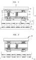
- Fig. 1 illustrates a microelectronic assembly 100 in accordance with an embodiment of the invention.
- the microelectronic package includes first and second microelectronic elements 102, 112, each having a contact-bearing front surface 104, 114 which faces toward an interposer 120 disposed between the microelectronic elements.
- Each microelectronic element can be, for example, an integrated circuit embodied in a semiconductor chip, which can include silicon, an alloy of silicon, or other semiconductor material such as a III-V semiconductor material or II-VI semiconductor material. As seen in the enlarged view of Fig.
- chip 102 has a front surface 104, also referred to as a contact-bearing face, being a major surface of the chip, with a first region 105 of the chip at the front face.
- the second chip 112 can have the same structure as chip 102.
- the first region 105 includes a dielectric region, which typically includes a plurality of wiring layers having dielectric layers disposed between and around the wiring layers.
- the dielectric region can include one or more layers of dielectric material having a low dielectric constant, i.e., a "low-k" dielectric layer.
- Low-k dielectric materials include porous silicon dioxide, carbon-doped silicon dioxide, polymeric dielectrics, and porous polymeric dielectrics, among others.
- the dielectric layer can have substantial porosity, which reduces the dielectric constant of the dielectric material relative to a nonporous layer of the same material.
- Dielectric materials typically have a dielectric constant significantly above 1.0, but air which occupies open spaces within a porous dielectric material has a dielectric constant of about 1.0. In this way, some dielectric materials can achieve reductions in the dielectric constant by having substantial porosity.
- some low-k dielectric materials such as polymeric dielectric materials and porous dielectric materials, withstand much less mechanical stress than traditional dielectric materials.
- Particular types of operating environments and ways that the microelectronic element may be tested can present stress at or near a limit that the low-k dielectric material can tolerate.
- the microelectronic assemblies described herein provide improved protection for the low-k dielectric layer of a microelectronic element by moving the locations where stress is applied to the microelectronic element away from the low-k dielectric layer within region 105. In this way, manufacturing, operation and testing apply much reduced stresses to the low-k dielectric layer, thus protecting the low-k dielectric layer.
- Layer 105 also includes active semiconductor devices (e.g., transistors, diodes, or other active devices), which are ultimately connected by the wiring layers with a plurality of electrically conductive pads 106 at the front face.
- active semiconductor devices e.g., transistors, diodes, or other active devices
- the first region 105 may also include a buried dielectric layer which underlies the active semiconductor devices.
- the first region 105 may separate a second region 107 of the chip from the front face 104.
- the first region typically has a thickness of 0.1 micron to 5 microns, and typically cannot be thinned.
- the second region 107 typically consists essentially of semiconductor material (typically either monocrystalline or polycrystalline) and typically has a thickness under 20 microns, the thickness typically being determined by the degree to which an initial semiconductor wafer has been thinned during processing.
- the chip may have only the first region 105 and the second region 107 may not be present.
- the structurally interposer 120 to which the microelectronic elements 102, 112 are mounted structurally supports the microelectronic elements, enabling the thicknesses of the microelectronic elements 102, 112 to be reduced to an exceptional degree. Also, with the dielectric region 105 the of each microelectronic element facing the interposer,
- microelectronic elements can be bonded together with the interposer 120, such as with adhesive 101.
- Other possible bonding materials can include glass, which in a particular embodiment, can be doped and can have a glass transition temperature below 500 °C.
- microelectronic element 112 consists essentially of the same semiconductor material as the other microelectronic element 102.
- microelectronic element 110 can have a plurality of conductive via elements extending through openings in the microelectronic element for providing electrically conductive connections with the conductive pads 106, 116.
- the microelectronic elements 102, 112 can be electrically connected together through electrically conductive elements 118 extending through the conductive pads 106, 116 and the interposer 120 therebetween.
- the conductive elements 118 can include metal features which are formed by depositing a metal in contact with exposed surfaces of the conductive pads 106, 116.
- Various metal deposition steps can be used to form the conductive elements, as described in further detail below.
- the conductive elements 118 can be conductively bonded, similar to flip-chip manner, to contacts 124 exposed at a surface of a dielectric element 126, such as through masses 128 of a bond metal, e.g., solder, tin, indium, or a combination thereof.
- the dielectric element can have a plurality of terminals 130 for further electrically connecting the package 100 to corresponding contacts 136 of a circuit panel 134, such as through conductive masses 132, e.g., solder balls, projecting away from the dielectric element 126.
- Fig. 1 illustrates the package 100 prior to joining the circuit panel 134 thereto.
- Fig. 2 illustrates a microelectronic assembly which includes the package 100 and the circuit panel 134 joined thereto.
- a heat spreader 140 may be thermally coupled to a rear surface 137 of microelectronic element 102, such as through a thermally conductive material 142, e.g., a thermally conductive grease, thermally conductive adhesive, or a joining metal having a relatively low melting temperature such as solder, tin, indium, gold, or other material.
- a thermally conductive material 142 e.g., a thermally conductive grease, thermally conductive adhesive, or a joining metal having a relatively low melting temperature such as solder, tin, indium, gold, or other material.
- a dielectric layer can separate the rear surface 137 of the microelectronic element 102 from such thermally and electrically conductive material 142.
- the microelectronic assembly or package 100 enables the thicknesses of the microelectronic elements 102, 112 to be reduced to an exceptional degree.
- the thickness of each microelectronic element 102 or 112 may be only the thickness of the first region 105 ( Fig. 1A ) or such thickness plus a small thickness of a second region 107.
- the reduced thickness can enable remarkably effective and even heat transfer to be achieved with heat spreader 140.
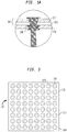
- Fig. 3 is a view looking toward the rear surface 115 of the microelectronic element 112 of the package illustrating conductive elements 118 exposed at the rear surface, which are shown arranged in an area array.
- the conductive elements 118 extend within second openings 123 and are connected to conductive pads 116 exposed at the front surface 103 ( Fig. 1 ) of microelectronic element 110, which can also be arranged in an area array.
- the conductive pads 116 of microelectronic element have a different arrangement, such as can be arranged adjacent peripheral edges 144, or can be arranged centrally to the front surface, the conductive elements 118 typically have a matching pattern.
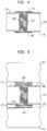
- FIG. 4 is a fragmentary sectional view showing an interposer 220 having a through hole 222 through which a conductive via 224 extends.
- the via 224 can terminate in first and second conductive pads 226, 228 exposed at first and second major surfaces 227, 229 of the interposer, respectively.
- the interposer may have a linear coefficient of thermal expansion (CTE- ⁇ ) which is less than about 10 parts per million per degree Celsius, i.e., "less than 10 ppm/°C".
- CTE- ⁇ linear coefficient of thermal expansion
- a dielectric layer 230 can overlie the first and second major surfaces and line the through hole 222 for insulating the via 224 and pads 226, 228 from the body of the interposer 220. Then, as illustrated in Fig.
- a first wafer 202 and a second wafer 212 are attached to the interposer with the front surfaces 203, 213 of the wafers facing the first and second interposer surfaces 227, 229, respectively.
- An adhesive or other dielectric material 201 e.g., glass, can be used for attaching the interposer with the wafers.
- the wafers are attached to the interposer such that conductive pads of each wafer are juxtaposed with the pads of the interposer. For example, a conductive pad 204 of first wafer 202 is juxtaposed with interposer pad 226 and a conductive pad 214 of second wafer 212 is juxtaposed with interposer pad 228.
- each wafer 202, 212 may have a thickness 231 which corresponds to the thickness of the non-thinnable region 105 ( Fig. 1A ) as described above, or may have a greater thickness which may include some material of region 107 ( Fig. 1A ) underlying the non-thinnable region.
- region 107 of one or both wafers 202, 212 may have a thickness of up to 20 microns.
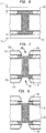
- Fig. 7 illustrates a subsequent stage of processing after which first and second openings 206, 216 have been formed that extend through the thickness of each wafer including the conductive pads 204, 214 thereon.
- Such openings can be made by etching, laser patterning, sandblasting, mechanical milling, or other technique applied to the semiconductor material of each wafer, for example.
- dielectric layers 232 can be formed on interior walls of the openings, after which the openings can be extended through the respective pads 204, 214.
- the process of forming the openings 206, 216 and the dielectric layers 232 can be as generally described in any or all of United States Patent Publication No.
- the dielectric layers 232 can be formed selectively onto exposed semiconductive or conductive surfaces within the openings 206, 216 and on the exposed faces of the microelectronic elements by electrophoretic or electrolytic deposition.
- Fig. 8 illustrates an optional step in which portions of a dielectric or bonding material between the juxtaposed surfaces of the wafer pads 204, 214 and the interposer pads 226, 228, respectively, are removed.
- one or more layers of metal can be deposited into the openings 206, 216 to form conductive elements 236, 238 which are exposed at respective outwardly facing surfaces 237, 239 of the microelectronic assembly.
- the conductive elements 236, 238 contact the conductive pads 204, 214 of the respective wafers 202, 212 and are electrically coupled together through the interposer pads 226, 228 and via 224 extending through the interposer.
- the opening 222 through which the via 224 extends intersects the openings 206, 216 extending through the first and second wafers 202, 212.
- the conductive elements in one or both of the wafers 202, 212 can be displaced in one or more lateral directions 240 (a direction in which interposer major surface 227 extends) from the via 224. In the case shown in Fig.
- both conductive elements 236, 238 can be displaced from the via in the same direction, and neither of the openings 206, 216 in which the conductive elements are formed intersects the corresponding interposer opening 222 through which via 224 extends and electrically connects the conductive elements 236, 238.
- interior surfaces of the openings 216, 206 in the microelectronic elements 202, 212 can extend in first and second directions relative to the respective first surface 104 of each microelectronic element to define a substantial angle 109.
- electrical connection between the interposer via 224 and the pads 204, 214 can be provided in one or more ways.
- a microelectronic element 212 can have a trace 244 extending away from conductive pad 214 towards the interposer 220 and the trace 244 can be conductively bonded to the via 224 of interposer, such as by using a joining metal 245 such as solder, tin or indium, diffusion bonding, or alternatively by direct metal to metal joining under heat and pressure.
- the interposer 220 can have an electrically conductive trace 242 which extends away from the via 224 in a direction 240 in which the first major surface 227 of the interposer extends. In this case, the fabrication of conductive element 236 forms an electrical connection between the pad 204 of first wafer and the trace 242 of the interposer.
- Fig. 11 illustrates another example in which conductive elements 236, 238 are displaced from one another in a direction 240.
- a further variation is shown in which the opening 322 in the interposer 320 is tapered such that its width becomes smaller in a direction towards the front surface of one of the microelectronic elements 202.
- dielectric layers 307, 317 can be formed on walls of the openings and the first surfaces.
- portions of the dielectric material, e.g., adhesive, between juxtaposed surfaces of the conductive pads 304, 314 and the corresponding bonding surfaces 326, 328 of the interposer via can be removed.
- FIG. 14 illustrates the microelectronic assembly after the conductive elements 336, 338 have been formed in contact with corresponding surfaces of the interposer via, wherein the deposited conductive material, e.g., deposited metal, fills the spaces between surfaces of the conductive pads 304, 314 and corresponding surfaces 326, 328 of the interposer via which are juxtaposed therewith.
- the deposited conductive material e.g., deposited metal
- Fig. 15 illustrates a further variation in which the conductive element 424 extending through the interposer opening has a shape, e.g., frusto-conical shape, which does not conform to a contour of the interior surface of the interposer opening 422.
- a fabrication method of the structure shown in Fig. 15 may also vary from that described above ( Figs. 4-14 ).
- the interposer 420 when the interposer 420 is joined with the microelectronic elements 402, 412, the interposer can have an opening 422 extending between first and second major surfaces which is filled with a dielectric material 426.
- the material removal process is continued through the adhesive or bonding layer 401 and through the region of dielectric material 426 until an upper surface 414a of conductive pad 414 is exposed within the opening 406. Thereafter, the opening 406 can be filled with one or more layers or metal or conductive compound of a metal to form the conductive element 436 extending through microelectronic element 402 and interposer 420.
- Fig. 16 illustrates a variation of the structure shown in Fig. 15 , in which the conductive element 536 is formed as a hollow structure lining an interior surface of a dielectric layer 407 within the opening 406 but not filling the opening.
- the conductive element 536 contacts an upper surface 414a of a conductive pad 414 exposed within the opening 406.
- Fig. 17 illustrates a further variation in which the opening 506 extends through a thickness of both conductive pads 504, 514, such that the conductive elements 636, 638 when formed can be in direct contact with each other.
- Fig. 18 illustrates a variation of the above-described embodiment ( Fig. 11 ) in which the interposer 720 embodies one or more passive circuit elements.
- the interposer can embody a first capacitor 750 having electrodes 752, 754 electrically connected with respective traces 756, 758 extending along a major surface 751 of the interposer 720.
- the interposer can embody a second capacitor 760 having electrodes 762, 764 electrically connected with respective traces 766, 768 extending along major surface 761 of the interposer 720.
- traces 758, 766 can be connected through further conductive elements 736, 738 to conductive pads which in operation of the assembly carry a time-varying signal, while other traces 756, 768 can be connected to one or more conductive pads (not shown) which in operation of the assembly carry a reference potential such as ground or a power supply voltage.
- the passive circuit elements can include one or more of: an inductor, a resistor, or other passive circuit element, being disposed as seen in Fig. 18 and having an electrical interconnection arrangement as seen, for example, in Fig. 18 .
- the structure and fabrication of the microelectronic assemblies and incorporation thereof into higher-level assemblies can include structure, and fabrication steps which are described in one or more of the following commonly owned co-pending applications of Oganesian et al. filed on even date herewith: "STACKED MICROELECTRONIC ASSEMBLY WITH TSVS FORMED IN STAGES AND CARRIER ABOVE CHIP" ( U.S. Provisional Application No. 61/419,033 ; Attorney Docket No. Tessera 3.8-619); and "STACKED MICROELECTRONIC ASSEMBLY WITH TSVS FORMED IN STAGES WITH PLURAL ACTIVE CHIPS" ( U.S. Provisional Application No. 61/419,037 ; Attorney Docket No.
- a processor and memory used with the processor includes a structure 806 as described above in conjunction with other electronic components 808 and 810.
- component 808 is a semiconductor chip whereas component 810 is a display screen, but any other components can be used.
- the structure 806 as described above may be, for example, a microelectronic assembly 100 as discussed above in connection with Fig. 1 , 9 , 10 , 14 , 15, 16 , 18 . In a further variant, both may be provided, and any number of such structures may be used. Structure 806 and components 808 and 810 are mounted in a common housing 801, schematically depicted in broken lines, and are electrically interconnected with one another as necessary to form the desired circuit.
- the system includes a circuit panel 802 such as a flexible printed circuit board, and the circuit panel includes numerous conductors 804, of which only one is depicted in Fig. 19 , interconnecting the components with one another.
- the housing 801 is depicted as a portable housing of the type usable, for example, in a cellular telephone or personal digital assistant, and screen 810 is exposed at the surface of the housing.
- structure 806 includes a light-sensitive element such as an imaging chip
- a lens 811 or other optical device also may be provided for routing light to the structure.
- the simplified system shown in Fig. 19 is merely exemplary; other systems, including systems commonly regarded as fixed structures, such as desktop computers, routers and the like can be made using the structures discussed above.
- the present invention enjoys wide industrial applicability including, but not limited to, microelectronic assemblies and methods of fabricating microelectronic assemblies.
Landscapes
- Engineering & Computer Science (AREA)
- Microelectronics & Electronic Packaging (AREA)
- Power Engineering (AREA)
- Computer Hardware Design (AREA)
- General Physics & Mathematics (AREA)
- Condensed Matter Physics & Semiconductors (AREA)
- Physics & Mathematics (AREA)
- Manufacturing & Machinery (AREA)
- Chemical & Material Sciences (AREA)
- Materials Engineering (AREA)
- Ceramic Engineering (AREA)
- Internal Circuitry In Semiconductor Integrated Circuit Devices (AREA)
- Wire Bonding (AREA)
- Production Of Multi-Layered Print Wiring Board (AREA)
Applications Claiming Priority (2)
| Application Number | Priority Date | Filing Date | Title |
|---|---|---|---|
| US12/958,866 US8637968B2 (en) | 2010-12-02 | 2010-12-02 | Stacked microelectronic assembly having interposer connecting active chips |
| PCT/US2011/063025 WO2012075371A1 (en) | 2010-12-02 | 2011-12-02 | Stacked microelectronic assembly having interposer connecting active chips |
Publications (2)
| Publication Number | Publication Date |
|---|---|
| EP2647046A1 EP2647046A1 (en) | 2013-10-09 |
| EP2647046B1 true EP2647046B1 (en) | 2020-11-18 |
Family
ID=45373838
Family Applications (1)
| Application Number | Title | Priority Date | Filing Date |
|---|---|---|---|
| EP11799219.8A Active EP2647046B1 (en) | 2010-12-02 | 2011-12-02 | Stacked microelectronic assembly having interposer connecting active chips |
Country Status (7)
Families Citing this family (21)
| Publication number | Priority date | Publication date | Assignee | Title |
|---|---|---|---|---|
| US8569876B2 (en) | 2006-11-22 | 2013-10-29 | Tessera, Inc. | Packaged semiconductor chips with array |
| US8329578B2 (en) * | 2009-03-27 | 2012-12-11 | Taiwan Semiconductor Manufacturing Company, Ltd. | Via structure and via etching process of forming the same |
| US9640437B2 (en) | 2010-07-23 | 2017-05-02 | Tessera, Inc. | Methods of forming semiconductor elements using micro-abrasive particle stream |
| US8847380B2 (en) * | 2010-09-17 | 2014-09-30 | Tessera, Inc. | Staged via formation from both sides of chip |
| US8736066B2 (en) | 2010-12-02 | 2014-05-27 | Tessera, Inc. | Stacked microelectronic assemby with TSVS formed in stages and carrier above chip |
| US8587126B2 (en) * | 2010-12-02 | 2013-11-19 | Tessera, Inc. | Stacked microelectronic assembly with TSVs formed in stages with plural active chips |
| US20130073755A1 (en) * | 2011-09-20 | 2013-03-21 | Advanced Micro Devices, Inc. | Device protocol translator for connection of external devices to a processing unit package |
| TWI500125B (zh) * | 2012-12-21 | 2015-09-11 | Unimicron Technology Corp | 電子元件封裝之製法 |
| CN103903990B (zh) * | 2012-12-28 | 2016-12-28 | 欣兴电子股份有限公司 | 电子组件封装的制法 |
| US9237648B2 (en) | 2013-02-25 | 2016-01-12 | Invensas Corporation | Carrier-less silicon interposer |
| US9691693B2 (en) | 2013-12-04 | 2017-06-27 | Invensas Corporation | Carrier-less silicon interposer using photo patterned polymer as substrate |
| US9437536B1 (en) | 2015-05-08 | 2016-09-06 | Invensas Corporation | Reversed build-up substrate for 2.5D |
| JP6502751B2 (ja) * | 2015-05-29 | 2019-04-17 | 東芝メモリ株式会社 | 半導体装置および半導体装置の製造方法 |
| US10211160B2 (en) | 2015-09-08 | 2019-02-19 | Invensas Corporation | Microelectronic assembly with redistribution structure formed on carrier |
| US9666560B1 (en) | 2015-11-25 | 2017-05-30 | Invensas Corporation | Multi-chip microelectronic assembly with built-up fine-patterned circuit structure |
| US10204889B2 (en) * | 2016-11-28 | 2019-02-12 | Taiwan Semiconductor Manufacturing Co., Ltd. | Package structure and method of forming thereof |
| US11652036B2 (en) * | 2018-04-02 | 2023-05-16 | Santa Clara | Via-trace structures |
| FR3080218B1 (fr) * | 2018-04-11 | 2022-02-11 | St Microelectronics Grenoble 2 | Dispositif electronique comprenant des puces electroniques |
| EP3807927A4 (en) * | 2018-06-13 | 2022-02-23 | Invensas Bonding Technologies, Inc. | TSV AS PAD |
| US11309285B2 (en) * | 2019-06-13 | 2022-04-19 | Micron Technology, Inc. | Three-dimensional stacking semiconductor assemblies and methods of manufacturing the same |
| US11610833B2 (en) * | 2020-10-22 | 2023-03-21 | Nanya Technology Corporation | Conductive feature with non-uniform critical dimension and method of manufacturing the same |
Citations (1)
| Publication number | Priority date | Publication date | Assignee | Title |
|---|---|---|---|---|
| US20100230795A1 (en) * | 2009-03-13 | 2010-09-16 | Tessera Technologies Hungary Kft. | Stacked microelectronic assemblies having vias extending through bond pads |
Family Cites Families (224)
| Publication number | Priority date | Publication date | Assignee | Title |
|---|---|---|---|---|
| NL8403613A (nl) | 1984-11-28 | 1986-06-16 | Philips Nv | Elektronenbundelinrichting en halfgeleiderinrichting voor een dergelijke inrichting. |
| US4765864A (en) | 1987-07-15 | 1988-08-23 | Sri International | Etching method for producing an electrochemical cell in a crystalline substrate |
| EP0316799B1 (en) | 1987-11-13 | 1994-07-27 | Nissan Motor Co., Ltd. | Semiconductor device |
| US5229647A (en) | 1991-03-27 | 1993-07-20 | Micron Technology, Inc. | High density data storage using stacked wafers |
| US5322816A (en) | 1993-01-19 | 1994-06-21 | Hughes Aircraft Company | Method for forming deep conductive feedthroughs |
| US5380681A (en) | 1994-03-21 | 1995-01-10 | United Microelectronics Corporation | Three-dimensional multichip package and methods of fabricating |
| IL110261A0 (en) | 1994-07-10 | 1994-10-21 | Schellcase Ltd | Packaged integrated circuit |
| GB2292015B (en) | 1994-07-29 | 1998-07-22 | Plessey Semiconductors Ltd | Trimmable inductor structure |
| US6826827B1 (en) | 1994-12-29 | 2004-12-07 | Tessera, Inc. | Forming conductive posts by selective removal of conductive material |
| US5703408A (en) | 1995-04-10 | 1997-12-30 | United Microelectronics Corporation | Bonding pad structure and method thereof |
| US6284563B1 (en) | 1995-10-31 | 2001-09-04 | Tessera, Inc. | Method of making compliant microelectronic assemblies |
| US6013948A (en) | 1995-11-27 | 2000-01-11 | Micron Technology, Inc. | Stackable chip scale semiconductor package with mating contacts on opposed surfaces |
| US5686762A (en) | 1995-12-21 | 1997-11-11 | Micron Technology, Inc. | Semiconductor device with improved bond pads |
| TW343210B (en) | 1996-01-12 | 1998-10-21 | Matsushita Electric Works Ltd | Process for impregnating a substrate, impregnated substrate and products thereof |
| US5808874A (en) | 1996-05-02 | 1998-09-15 | Tessera, Inc. | Microelectronic connections with liquid conductive elements |
| US5700735A (en) | 1996-08-22 | 1997-12-23 | Taiwan Semiconductor Manufacturing Company, Ltd. | Method of forming bond pad structure for the via plug process |
| JP3620936B2 (ja) | 1996-10-11 | 2005-02-16 | 浜松ホトニクス株式会社 | 裏面照射型受光デバイスおよびその製造方法 |
| US6143396A (en) | 1997-05-01 | 2000-11-07 | Texas Instruments Incorporated | System and method for reinforcing a bond pad |
| US6573609B2 (en) | 1997-11-25 | 2003-06-03 | Tessera, Inc. | Microelectronic component with rigid interposer |
| EP0926723B1 (en) | 1997-11-26 | 2007-01-17 | STMicroelectronics S.r.l. | Process for forming front-back through contacts in micro-integrated electronic devices |
| US6620731B1 (en) | 1997-12-18 | 2003-09-16 | Micron Technology, Inc. | Method for fabricating semiconductor components and interconnects with contacts on opposing sides |
| US6879049B1 (en) | 1998-01-23 | 2005-04-12 | Rohm Co., Ltd. | Damascene interconnection and semiconductor device |
| US6982475B1 (en) | 1998-03-20 | 2006-01-03 | Mcsp, Llc | Hermetic wafer scale integrated circuit structure |
| US5986343A (en) | 1998-05-04 | 1999-11-16 | Lucent Technologies Inc. | Bond pad design for integrated circuits |
| US6492201B1 (en) | 1998-07-10 | 2002-12-10 | Tessera, Inc. | Forming microelectronic connection components by electrophoretic deposition |
| US6103552A (en) | 1998-08-10 | 2000-08-15 | Lin; Mou-Shiung | Wafer scale packaging scheme |
| US6261865B1 (en) | 1998-10-06 | 2001-07-17 | Micron Technology, Inc. | Multi chip semiconductor package and method of construction |
| JP2000195896A (ja) | 1998-12-25 | 2000-07-14 | Nec Corp | 半導体装置 |
| US6181016B1 (en) | 1999-06-08 | 2001-01-30 | Winbond Electronics Corp | Bond-pad with a single anchoring structure |
| US6368410B1 (en) | 1999-06-28 | 2002-04-09 | General Electric Company | Semiconductor processing article |
| US6168965B1 (en) | 1999-08-12 | 2001-01-02 | Tower Semiconductor Ltd. | Method for making backside illuminated image sensor |
| JP4139533B2 (ja) | 1999-09-10 | 2008-08-27 | 大日本印刷株式会社 | 半導体装置とその製造方法 |
| US6277669B1 (en) | 1999-09-15 | 2001-08-21 | Industrial Technology Research Institute | Wafer level packaging method and packages formed |
| JP2001102479A (ja) * | 1999-09-27 | 2001-04-13 | Toshiba Corp | 半導体集積回路装置およびその製造方法 |
| JP2001127243A (ja) | 1999-10-26 | 2001-05-11 | Sharp Corp | 積層半導体装置 |
| US6507113B1 (en) | 1999-11-19 | 2003-01-14 | General Electric Company | Electronic interface structures and methods of fabrication |
| JP3684978B2 (ja) | 2000-02-03 | 2005-08-17 | セイコーエプソン株式会社 | 半導体装置およびその製造方法ならびに電子機器 |
| US6498387B1 (en) | 2000-02-15 | 2002-12-24 | Wen-Ken Yang | Wafer level package and the process of the same |
| US6586955B2 (en) | 2000-03-13 | 2003-07-01 | Tessera, Inc. | Methods and structures for electronic probing arrays |
| JP3879816B2 (ja) | 2000-06-02 | 2007-02-14 | セイコーエプソン株式会社 | 半導体装置及びその製造方法、積層型半導体装置、回路基板並びに電子機器 |
| US6472247B1 (en) | 2000-06-26 | 2002-10-29 | Ricoh Company, Ltd. | Solid-state imaging device and method of production of the same |
| US6399892B1 (en) | 2000-09-19 | 2002-06-04 | International Business Machines Corporation | CTE compensated chip interposer |
| US6693358B2 (en) | 2000-10-23 | 2004-02-17 | Matsushita Electric Industrial Co., Ltd. | Semiconductor chip, wiring board and manufacturing process thereof as well as semiconductor device |
| JP3433193B2 (ja) | 2000-10-23 | 2003-08-04 | 松下電器産業株式会社 | 半導体チップおよびその製造方法 |
| EP1207015A3 (en) | 2000-11-17 | 2003-07-30 | Keltech Engineering, Inc. | Raised island abrasive, method of use and lapping apparatus |
| JP2002162212A (ja) | 2000-11-24 | 2002-06-07 | Foundation Of River & Basin Integrated Communications Japan | 堤体ひずみ計測センサ |
| US20020098620A1 (en) | 2001-01-24 | 2002-07-25 | Yi-Chuan Ding | Chip scale package and manufacturing method thereof |
| KR100352236B1 (ko) | 2001-01-30 | 2002-09-12 | 삼성전자 주식회사 | 접지 금속층을 갖는 웨이퍼 레벨 패키지 |
| US6867123B2 (en) | 2001-02-08 | 2005-03-15 | Renesas Technology Corp. | Semiconductor integrated circuit device and its manufacturing method |
| KR100364635B1 (ko) | 2001-02-09 | 2002-12-16 | 삼성전자 주식회사 | 칩-레벨에 형성된 칩 선택용 패드를 포함하는 칩-레벨3차원 멀티-칩 패키지 및 그 제조 방법 |
| US6498381B2 (en) | 2001-02-22 | 2002-12-24 | Tru-Si Technologies, Inc. | Semiconductor structures having multiple conductive layers in an opening, and methods for fabricating same |
| JP2002270718A (ja) | 2001-03-07 | 2002-09-20 | Seiko Epson Corp | 配線基板及びその製造方法、半導体装置及びその製造方法、回路基板並びに電子機器 |
| JP2002359347A (ja) | 2001-03-28 | 2002-12-13 | Seiko Epson Corp | 半導体装置及びその製造方法、回路基板並びに電子機器 |
| JP2002373957A (ja) | 2001-06-14 | 2002-12-26 | Shinko Electric Ind Co Ltd | 半導体装置及びその製造方法 |
| JP2003020404A (ja) | 2001-07-10 | 2003-01-24 | Hitachi Ltd | 耐熱性低弾性率材およびそれを用いた装置 |
| US6531384B1 (en) | 2001-09-14 | 2003-03-11 | Motorola, Inc. | Method of forming a bond pad and structure thereof |
| US20030059976A1 (en) | 2001-09-24 | 2003-03-27 | Nathan Richard J. | Integrated package and methods for making same |
| JP2003124393A (ja) | 2001-10-17 | 2003-04-25 | Hitachi Ltd | 半導体装置およびその製造方法 |
| US6727576B2 (en) | 2001-10-31 | 2004-04-27 | Infineon Technologies Ag | Transfer wafer level packaging |
| US20040051173A1 (en) | 2001-12-10 | 2004-03-18 | Koh Philip Joseph | High frequency interconnect system using micromachined plugs and sockets |
| TW544882B (en) | 2001-12-31 | 2003-08-01 | Megic Corp | Chip package structure and process thereof |
| TW517361B (en) | 2001-12-31 | 2003-01-11 | Megic Corp | Chip package structure and its manufacture process |
| US6743660B2 (en) | 2002-01-12 | 2004-06-01 | Taiwan Semiconductor Manufacturing Co., Ltd | Method of making a wafer level chip scale package |
| JP2003282791A (ja) | 2002-03-20 | 2003-10-03 | Fujitsu Ltd | 接触型センサ内蔵半導体装置及びその製造方法 |
| JP2003318178A (ja) | 2002-04-24 | 2003-11-07 | Seiko Epson Corp | 半導体装置及びその製造方法、回路基板並びに電子機器 |
| TWI229435B (en) | 2002-06-18 | 2005-03-11 | Sanyo Electric Co | Manufacture of semiconductor device |
| US6716737B2 (en) | 2002-07-29 | 2004-04-06 | Hewlett-Packard Development Company, L.P. | Method of forming a through-substrate interconnect |
| US7030010B2 (en) | 2002-08-29 | 2006-04-18 | Micron Technology, Inc. | Methods for creating electrophoretically insulated vias in semiconductive substrates and resulting structures |
| US6903442B2 (en) | 2002-08-29 | 2005-06-07 | Micron Technology, Inc. | Semiconductor component having backside pin contacts |
| US7329563B2 (en) | 2002-09-03 | 2008-02-12 | Industrial Technology Research Institute | Method for fabrication of wafer level package incorporating dual compliant layers |
| EP1551060B1 (en) | 2002-09-24 | 2012-08-15 | Hamamatsu Photonics K. K. | Photodiode array and method for manufacturing same |
| JP4440554B2 (ja) | 2002-09-24 | 2010-03-24 | 浜松ホトニクス株式会社 | 半導体装置 |
| JP2004128063A (ja) | 2002-09-30 | 2004-04-22 | Toshiba Corp | 半導体装置及びその製造方法 |
| US20040104454A1 (en) | 2002-10-10 | 2004-06-03 | Rohm Co., Ltd. | Semiconductor device and method of producing the same |
| TW569395B (en) | 2002-10-30 | 2004-01-01 | Intelligent Sources Dev Corp | Method of forming a stacked-gate cell structure and its NAND-type flash memory array |
| US20050012225A1 (en) | 2002-11-15 | 2005-01-20 | Choi Seung-Yong | Wafer-level chip scale package and method for fabricating and using the same |
| JP3918935B2 (ja) | 2002-12-20 | 2007-05-23 | セイコーエプソン株式会社 | 半導体装置の製造方法 |
| JP4072677B2 (ja) | 2003-01-15 | 2008-04-09 | セイコーエプソン株式会社 | 半導体チップ、半導体ウエハ、半導体装置及びその製造方法、回路基板並びに電子機器 |
| JP2004356618A (ja) * | 2003-03-19 | 2004-12-16 | Ngk Spark Plug Co Ltd | 中継基板、半導体素子付き中継基板、中継基板付き基板、半導体素子と中継基板と基板とからなる構造体、中継基板の製造方法 |
| SG137651A1 (en) | 2003-03-14 | 2007-12-28 | Micron Technology Inc | Microelectronic devices and methods for packaging microelectronic devices |
| JP3680839B2 (ja) | 2003-03-18 | 2005-08-10 | セイコーエプソン株式会社 | 半導体装置および半導体装置の製造方法 |
| US6841883B1 (en) | 2003-03-31 | 2005-01-11 | Micron Technology, Inc. | Multi-dice chip scale semiconductor components and wafer level methods of fabrication |
| US6908856B2 (en) | 2003-04-03 | 2005-06-21 | Interuniversitair Microelektronica Centrum (Imec) | Method for producing electrical through hole interconnects and devices made thereof |
| EP1519410A1 (en) | 2003-09-25 | 2005-03-30 | Interuniversitair Microelektronica Centrum vzw ( IMEC) | Method for producing electrical through hole interconnects and devices made thereof |
| JP4373695B2 (ja) | 2003-04-16 | 2009-11-25 | 浜松ホトニクス株式会社 | 裏面照射型光検出装置の製造方法 |
| DE10319538B4 (de) | 2003-04-30 | 2008-01-17 | Qimonda Ag | Halbleitervorrichtung und Verfahren zur Herstellung einer Halbleitereinrichtung |
| EP1482553A3 (en) | 2003-05-26 | 2007-03-28 | Sanyo Electric Co., Ltd. | Semiconductor device and manufacturing method thereof |
| US6972480B2 (en) | 2003-06-16 | 2005-12-06 | Shellcase Ltd. | Methods and apparatus for packaging integrated circuit devices |
| US6927156B2 (en) | 2003-06-18 | 2005-08-09 | Intel Corporation | Apparatus and method extending flip-chip pad structures for wirebonding on low-k dielectric silicon |
| JP3646720B2 (ja) | 2003-06-19 | 2005-05-11 | セイコーエプソン株式会社 | 半導体装置及びその製造方法、回路基板並びに電子機器 |
| US9530857B2 (en) | 2003-06-20 | 2016-12-27 | Tessera Advanced Technologies, Inc. | Electronic device, assembly and methods of manufacturing an electronic device including a vertical trench capacitor and a vertical interconnect |
| JP2005026405A (ja) | 2003-07-01 | 2005-01-27 | Sharp Corp | 貫通電極構造およびその製造方法、半導体チップならびにマルチチップ半導体装置 |
| JP2005045073A (ja) | 2003-07-23 | 2005-02-17 | Hamamatsu Photonics Kk | 裏面入射型光検出素子 |
| JP4499386B2 (ja) | 2003-07-29 | 2010-07-07 | 浜松ホトニクス株式会社 | 裏面入射型光検出素子の製造方法 |
| KR100537892B1 (ko) | 2003-08-26 | 2005-12-21 | 삼성전자주식회사 | 칩 스택 패키지와 그 제조 방법 |
| US7180149B2 (en) | 2003-08-28 | 2007-02-20 | Fujikura Ltd. | Semiconductor package with through-hole |
| JP2005093486A (ja) | 2003-09-12 | 2005-04-07 | Seiko Epson Corp | 半導体装置の製造方法及び半導体装置 |
| JP2005101268A (ja) | 2003-09-25 | 2005-04-14 | Sanyo Electric Co Ltd | 半導体装置の製造方法 |
| US20050095835A1 (en) | 2003-09-26 | 2005-05-05 | Tessera, Inc. | Structure and method of making capped chips having vertical interconnects |
| GB2406720B (en) | 2003-09-30 | 2006-09-13 | Agere Systems Inc | An inductor formed in an integrated circuit |
| US7495179B2 (en) | 2003-10-06 | 2009-02-24 | Tessera, Inc. | Components with posts and pads |
| TWI259564B (en) | 2003-10-15 | 2006-08-01 | Infineon Technologies Ag | Wafer level packages for chips with sawn edge protection |
| US7132743B2 (en) * | 2003-12-23 | 2006-11-07 | Intel Corporation | Integrated circuit package substrate having a thin film capacitor structure |
| TWI234244B (en) | 2003-12-26 | 2005-06-11 | Intelligent Sources Dev Corp | Paired stack-gate flash cell structure and its contactless NAND-type flash memory arrays |
| US20050156330A1 (en) | 2004-01-21 | 2005-07-21 | Harris James M. | Through-wafer contact to bonding pad |
| US7026175B2 (en) | 2004-03-29 | 2006-04-11 | Applied Materials, Inc. | High throughput measurement of via defects in interconnects |
| US7368695B2 (en) | 2004-05-03 | 2008-05-06 | Tessera, Inc. | Image sensor package and fabrication method |
| US20050248002A1 (en) | 2004-05-07 | 2005-11-10 | Michael Newman | Fill for large volume vias |
| KR100618837B1 (ko) | 2004-06-22 | 2006-09-01 | 삼성전자주식회사 | 웨이퍼 레벨 패키지를 위한 얇은 웨이퍼들의 스택을형성하는 방법 |
| US7232754B2 (en) | 2004-06-29 | 2007-06-19 | Micron Technology, Inc. | Microelectronic devices and methods for forming interconnects in microelectronic devices |
| JP2006019455A (ja) | 2004-06-30 | 2006-01-19 | Nec Electronics Corp | 半導体装置およびその製造方法 |
| JP4343044B2 (ja) * | 2004-06-30 | 2009-10-14 | 新光電気工業株式会社 | インターポーザ及びその製造方法並びに半導体装置 |
| KR100605314B1 (ko) | 2004-07-22 | 2006-07-28 | 삼성전자주식회사 | 재배선 보호 피막을 가지는 웨이퍼 레벨 패키지의 제조 방법 |
| US7750487B2 (en) | 2004-08-11 | 2010-07-06 | Intel Corporation | Metal-metal bonding of compliant interconnect |
| US7598167B2 (en) | 2004-08-24 | 2009-10-06 | Micron Technology, Inc. | Method of forming vias in semiconductor substrates without damaging active regions thereof and resulting structures |
| US7378342B2 (en) | 2004-08-27 | 2008-05-27 | Micron Technology, Inc. | Methods for forming vias varying lateral dimensions |
| US7129567B2 (en) | 2004-08-31 | 2006-10-31 | Micron Technology, Inc. | Substrate, semiconductor die, multichip module, and system including a via structure comprising a plurality of conductive elements |
| KR100604049B1 (ko) | 2004-09-01 | 2006-07-24 | 동부일렉트로닉스 주식회사 | 반도체 칩 패키지 및 그 제조방법 |
| US7300857B2 (en) | 2004-09-02 | 2007-11-27 | Micron Technology, Inc. | Through-wafer interconnects for photoimager and memory wafers |
| JP4139803B2 (ja) | 2004-09-28 | 2008-08-27 | シャープ株式会社 | 半導体装置の製造方法 |
| JP4246132B2 (ja) | 2004-10-04 | 2009-04-02 | シャープ株式会社 | 半導体装置およびその製造方法 |
| US7819119B2 (en) | 2004-10-08 | 2010-10-26 | Ric Investments, Llc | User interface having a pivotable coupling |
| KR100676493B1 (ko) | 2004-10-08 | 2007-02-01 | 디엔제이 클럽 인코 | 재배선 기판을 이용한 웨이퍼 레벨 칩 스케일 패키지의제조 방법 |
| US7081408B2 (en) | 2004-10-28 | 2006-07-25 | Intel Corporation | Method of creating a tapered via using a receding mask and resulting structure |
| JP4873517B2 (ja) | 2004-10-28 | 2012-02-08 | オンセミコンダクター・トレーディング・リミテッド | 半導体装置及びその製造方法 |
| US20060278997A1 (en) | 2004-12-01 | 2006-12-14 | Tessera, Inc. | Soldered assemblies and methods of making the same |
| JP4795677B2 (ja) | 2004-12-02 | 2011-10-19 | ルネサスエレクトロニクス株式会社 | 半導体装置およびそれを用いた半導体モジュール、ならびに半導体装置の製造方法 |
| JP4290158B2 (ja) | 2004-12-20 | 2009-07-01 | 三洋電機株式会社 | 半導体装置 |
| KR20060087273A (ko) | 2005-01-28 | 2006-08-02 | 삼성전기주식회사 | 반도체 패키지및 그 제조방법 |
| US7675153B2 (en) | 2005-02-02 | 2010-03-09 | Kabushiki Kaisha Toshiba | Semiconductor device having semiconductor chips stacked and mounted thereon and manufacturing method thereof |
| US7538032B2 (en) | 2005-06-23 | 2009-05-26 | Teledyne Scientific & Imaging, Llc | Low temperature method for fabricating high-aspect ratio vias and devices fabricated by said method |
| TWI244186B (en) | 2005-03-02 | 2005-11-21 | Advanced Semiconductor Eng | Semiconductor package and method for manufacturing the same |
| TWI264807B (en) | 2005-03-02 | 2006-10-21 | Advanced Semiconductor Eng | Semiconductor package and method for manufacturing the same |
| US20060264029A1 (en) | 2005-05-23 | 2006-11-23 | Intel Corporation | Low inductance via structures |
| US7795134B2 (en) | 2005-06-28 | 2010-09-14 | Micron Technology, Inc. | Conductive interconnect structures and formation methods using supercritical fluids |
| US7834273B2 (en) * | 2005-07-07 | 2010-11-16 | Ibiden Co., Ltd. | Multilayer printed wiring board |
| JP4694305B2 (ja) | 2005-08-16 | 2011-06-08 | ルネサスエレクトロニクス株式会社 | 半導体ウエハの製造方法 |
| US20070049470A1 (en) | 2005-08-29 | 2007-03-01 | Johnson Health Tech Co., Ltd. | Rapid circuit training machine with dual resistance |
| US20070052050A1 (en) | 2005-09-07 | 2007-03-08 | Bart Dierickx | Backside thinned image sensor with integrated lens stack |
| JP2007157844A (ja) | 2005-12-01 | 2007-06-21 | Sharp Corp | 半導体装置、および半導体装置の製造方法 |
| US20070126085A1 (en) | 2005-12-02 | 2007-06-07 | Nec Electronics Corporation | Semiconductor device and method of manufacturing the same |
| US7456479B2 (en) | 2005-12-15 | 2008-11-25 | United Microelectronics Corp. | Method for fabricating a probing pad of an integrated circuit chip |
| JP4826248B2 (ja) | 2005-12-19 | 2011-11-30 | Tdk株式会社 | Ic内蔵基板の製造方法 |
| KR100714310B1 (ko) | 2006-02-23 | 2007-05-02 | 삼성전자주식회사 | 변압기 또는 안테나를 구비하는 반도체 패키지들 |
| US20080002460A1 (en) | 2006-03-01 | 2008-01-03 | Tessera, Inc. | Structure and method of making lidded chips |
| JP4659660B2 (ja) | 2006-03-31 | 2011-03-30 | Okiセミコンダクタ株式会社 | 半導体装置の製造方法 |
| JP2007311676A (ja) | 2006-05-22 | 2007-11-29 | Sony Corp | 半導体装置とその製造方法 |
| KR100837269B1 (ko) | 2006-05-22 | 2008-06-11 | 삼성전자주식회사 | 웨이퍼 레벨 패키지 및 그 제조 방법 |
| JP4950559B2 (ja) | 2006-05-25 | 2012-06-13 | パナソニック株式会社 | スルーホール電極の形成方法 |
| US7605019B2 (en) * | 2006-07-07 | 2009-10-20 | Qimonda Ag | Semiconductor device with stacked chips and method for manufacturing thereof |
| KR100750741B1 (ko) | 2006-09-15 | 2007-08-22 | 삼성전기주식회사 | 캡 웨이퍼, 이를 구비한 반도체 칩, 및 그 제조방법 |
| US7531445B2 (en) | 2006-09-26 | 2009-05-12 | Hymite A/S | Formation of through-wafer electrical interconnections and other structures using a thin dielectric membrane |
| US20080079779A1 (en) | 2006-09-28 | 2008-04-03 | Robert Lee Cornell | Method for Improving Thermal Conductivity in Micro-Fluid Ejection Heads |
| JP2008091632A (ja) | 2006-10-02 | 2008-04-17 | Manabu Bonshihara | 半導体装置の外部回路接続部の構造及びその形成方法 |
| US7901989B2 (en) | 2006-10-10 | 2011-03-08 | Tessera, Inc. | Reconstituted wafer level stacking |
| US7719121B2 (en) | 2006-10-17 | 2010-05-18 | Tessera, Inc. | Microelectronic packages and methods therefor |
| US7759166B2 (en) | 2006-10-17 | 2010-07-20 | Tessera, Inc. | Microelectronic packages fabricated at the wafer level and methods therefor |
| US7807508B2 (en) | 2006-10-31 | 2010-10-05 | Tessera Technologies Hungary Kft. | Wafer-level fabrication of lidded chips with electrodeposited dielectric coating |
| US7935568B2 (en) | 2006-10-31 | 2011-05-03 | Tessera Technologies Ireland Limited | Wafer-level fabrication of lidded chips with electrodeposited dielectric coating |
| KR100830581B1 (ko) | 2006-11-06 | 2008-05-22 | 삼성전자주식회사 | 관통전극을 구비한 반도체 소자 및 그 형성방법 |
| US7781781B2 (en) | 2006-11-17 | 2010-08-24 | International Business Machines Corporation | CMOS imager array with recessed dielectric |
| US8569876B2 (en) | 2006-11-22 | 2013-10-29 | Tessera, Inc. | Packaged semiconductor chips with array |
| US7791199B2 (en) | 2006-11-22 | 2010-09-07 | Tessera, Inc. | Packaged semiconductor chips |
| US20080136038A1 (en) | 2006-12-06 | 2008-06-12 | Sergey Savastiouk | Integrated circuits with conductive features in through holes passing through other conductive features and through a semiconductor substrate |
| FR2911006A1 (fr) | 2007-01-03 | 2008-07-04 | St Microelectronics Sa | Puce de circuit electronique integre comprenant une inductance |
| JP2008177249A (ja) | 2007-01-16 | 2008-07-31 | Sharp Corp | 半導体集積回路のボンディングパッド、その製造方法、半導体集積回路、並びに電子機器 |
| US7518226B2 (en) | 2007-02-06 | 2009-04-14 | Stats Chippac Ltd. | Integrated circuit packaging system with interposer |
| KR101460141B1 (ko) | 2007-03-05 | 2014-12-02 | 인벤사스 코포레이션 | 관통 비아에 의해 전면 컨택트에 연결되는 배면 컨택트를 갖는 칩 |
| JP4380718B2 (ja) | 2007-03-15 | 2009-12-09 | ソニー株式会社 | 半導体装置の製造方法 |
| KR100845006B1 (ko) | 2007-03-19 | 2008-07-09 | 삼성전자주식회사 | 적층 칩 패키지 및 그 제조 방법 |
| JP2008258258A (ja) | 2007-04-02 | 2008-10-23 | Sanyo Electric Co Ltd | 半導体装置 |
| US7977155B2 (en) | 2007-05-04 | 2011-07-12 | Taiwan Semiconductor Manufacturing Company, Ltd. | Wafer-level flip-chip assembly methods |
| US20080284041A1 (en) | 2007-05-18 | 2008-11-20 | Samsung Electronics Co., Ltd. | Semiconductor package with through silicon via and related method of fabrication |
| JP4937842B2 (ja) | 2007-06-06 | 2012-05-23 | ルネサスエレクトロニクス株式会社 | 半導体装置およびその製造方法 |
| US7767497B2 (en) | 2007-07-12 | 2010-08-03 | Tessera, Inc. | Microelectronic package element and method of fabricating thereof |
| US7932179B2 (en) | 2007-07-27 | 2011-04-26 | Micron Technology, Inc. | Method for fabricating semiconductor device having backside redistribution layers |
| CN101809739B (zh) | 2007-07-27 | 2014-08-20 | 泰塞拉公司 | 具有后应用的衬垫延长部分的重构晶片堆封装 |
| CN101802990B (zh) | 2007-07-31 | 2013-03-13 | 数字光学欧洲有限公司 | 使用穿透硅通道的半导体封装方法 |
| KR101387701B1 (ko) * | 2007-08-01 | 2014-04-23 | 삼성전자주식회사 | 반도체 패키지 및 이의 제조방법 |
| US7902069B2 (en) | 2007-08-02 | 2011-03-08 | International Business Machines Corporation | Small area, robust silicon via structure and process |
| WO2009023462A1 (en) | 2007-08-10 | 2009-02-19 | Spansion Llc | Semiconductor device and method for manufacturing thereof |
| KR100885924B1 (ko) | 2007-08-10 | 2009-02-26 | 삼성전자주식회사 | 묻혀진 도전성 포스트를 포함하는 반도체 패키지 및 그제조방법 |
| KR100905784B1 (ko) | 2007-08-16 | 2009-07-02 | 주식회사 하이닉스반도체 | 반도체 패키지용 관통 전극 및 이를 갖는 반도체 패키지 |
| KR101213175B1 (ko) * | 2007-08-20 | 2012-12-18 | 삼성전자주식회사 | 로직 칩에 층층이 쌓인 메모리장치들을 구비하는반도체패키지 |
| JP2009088201A (ja) | 2007-09-28 | 2009-04-23 | Nec Electronics Corp | 半導体装置 |
| JP2009129953A (ja) | 2007-11-20 | 2009-06-11 | Hitachi Ltd | 半導体装置 |
| US20090127667A1 (en) | 2007-11-21 | 2009-05-21 | Powertech Technology Inc. | Semiconductor chip device having through-silicon-via (TSV) and its fabrication method |
| US7998524B2 (en) | 2007-12-10 | 2011-08-16 | Abbott Cardiovascular Systems Inc. | Methods to improve adhesion of polymer coatings over stents |
| US7446036B1 (en) | 2007-12-18 | 2008-11-04 | International Business Machines Corporation | Gap free anchored conductor and dielectric structure and method for fabrication thereof |
| US8084854B2 (en) * | 2007-12-28 | 2011-12-27 | Micron Technology, Inc. | Pass-through 3D interconnect for microelectronic dies and associated systems and methods |
| JP5515744B2 (ja) | 2008-02-21 | 2014-06-11 | 日本電気株式会社 | 配線基板及び半導体装置 |
| US20090212381A1 (en) | 2008-02-26 | 2009-08-27 | Tessera, Inc. | Wafer level packages for rear-face illuminated solid state image sensors |
| US7791174B2 (en) | 2008-03-07 | 2010-09-07 | Advanced Inquiry Systems, Inc. | Wafer translator having a silicon core isolated from signal paths by a ground plane |
| US7842548B2 (en) | 2008-04-22 | 2010-11-30 | Taiwan Semconductor Manufacturing Co., Ltd. | Fixture for P-through silicon via assembly |
| US7838967B2 (en) * | 2008-04-24 | 2010-11-23 | Powertech Technology Inc. | Semiconductor chip having TSV (through silicon via) and stacked assembly including the chips |
| US20090267183A1 (en) | 2008-04-28 | 2009-10-29 | Research Triangle Institute | Through-substrate power-conducting via with embedded capacitance |
| US7939449B2 (en) | 2008-06-03 | 2011-05-10 | Micron Technology, Inc. | Methods of forming hybrid conductive vias including small dimension active surface ends and larger dimension back side ends |
| US7863721B2 (en) | 2008-06-11 | 2011-01-04 | Stats Chippac, Ltd. | Method and apparatus for wafer level integration using tapered vias |
| US20100013060A1 (en) | 2008-06-22 | 2010-01-21 | Taiwan Semiconductor Manufacturing Company, Ltd. | Method of forming a conductive trench in a silicon wafer and silicon wafer comprising such trench |
| JP5183340B2 (ja) | 2008-07-23 | 2013-04-17 | 日本電波工業株式会社 | 表面実装型の発振器およびこの発振器を搭載した電子機器 |
| KR20100020718A (ko) * | 2008-08-13 | 2010-02-23 | 삼성전자주식회사 | 반도체 칩, 그 스택 구조 및 이들의 제조 방법 |
| US20100117242A1 (en) | 2008-11-10 | 2010-05-13 | Miller Gary L | Technique for packaging multiple integrated circuits |
| US7906404B2 (en) | 2008-11-21 | 2011-03-15 | Teledyne Scientific & Imaging, Llc | Power distribution for CMOS circuits using in-substrate decoupling capacitors and back side metal layers |
| US7939926B2 (en) | 2008-12-12 | 2011-05-10 | Qualcomm Incorporated | Via first plus via last technique for IC interconnects |
| JP5308145B2 (ja) | 2008-12-19 | 2013-10-09 | ルネサスエレクトロニクス株式会社 | 半導体装置 |
| US20100159699A1 (en) | 2008-12-19 | 2010-06-24 | Yoshimi Takahashi | Sandblast etching for through semiconductor vias |
| TWI366890B (en) | 2008-12-31 | 2012-06-21 | Ind Tech Res Inst | Method of manufacturing through-silicon-via and through-silicon-via structure |
| KR20100087566A (ko) | 2009-01-28 | 2010-08-05 | 삼성전자주식회사 | 반도체 소자 패키지의 형성방법 |
| US8158515B2 (en) | 2009-02-03 | 2012-04-17 | International Business Machines Corporation | Method of making 3D integrated circuits |
| US7998860B2 (en) | 2009-03-12 | 2011-08-16 | Micron Technology, Inc. | Method for fabricating semiconductor components using maskless back side alignment to conductive vias |
| TWI466258B (zh) * | 2009-04-10 | 2014-12-21 | Nanya Technology Corp | 電性通透連接及其形成方法 |
| US8263434B2 (en) * | 2009-07-31 | 2012-09-11 | Stats Chippac, Ltd. | Semiconductor device and method of mounting die with TSV in cavity of substrate for electrical interconnect of Fi-PoP |
| JP5715334B2 (ja) * | 2009-10-15 | 2015-05-07 | ルネサスエレクトロニクス株式会社 | 半導体装置 |
| US8008121B2 (en) * | 2009-11-04 | 2011-08-30 | Stats Chippac, Ltd. | Semiconductor package and method of mounting semiconductor die to opposite sides of TSV substrate |
| US8519538B2 (en) | 2010-04-28 | 2013-08-27 | Taiwan Semiconductor Manufacturing Company, Ltd. | Laser etch via formation |
| US8299608B2 (en) * | 2010-07-08 | 2012-10-30 | International Business Machines Corporation | Enhanced thermal management of 3-D stacked die packaging |
| US9640437B2 (en) | 2010-07-23 | 2017-05-02 | Tessera, Inc. | Methods of forming semiconductor elements using micro-abrasive particle stream |
| US8796135B2 (en) | 2010-07-23 | 2014-08-05 | Tessera, Inc. | Microelectronic elements with rear contacts connected with via first or via middle structures |
| US8598695B2 (en) | 2010-07-23 | 2013-12-03 | Tessera, Inc. | Active chip on carrier or laminated chip having microelectronic element embedded therein |
| US8697569B2 (en) | 2010-07-23 | 2014-04-15 | Tessera, Inc. | Non-lithographic formation of three-dimensional conductive elements |
| US8791575B2 (en) | 2010-07-23 | 2014-07-29 | Tessera, Inc. | Microelectronic elements having metallic pads overlying vias |
| US8686565B2 (en) | 2010-09-16 | 2014-04-01 | Tessera, Inc. | Stacked chip assembly having vertical vias |
| US8847380B2 (en) * | 2010-09-17 | 2014-09-30 | Tessera, Inc. | Staged via formation from both sides of chip |
| US8421193B2 (en) * | 2010-11-18 | 2013-04-16 | Nanya Technology Corporation | Integrated circuit device having through via and method for preparing the same |
-
2010
- 2010-12-02 US US12/958,866 patent/US8637968B2/en active Active
-
2011
- 2011-12-02 WO PCT/US2011/063025 patent/WO2012075371A1/en unknown
- 2011-12-02 EP EP11799219.8A patent/EP2647046B1/en active Active
- 2011-12-02 CN CN201180066393.0A patent/CN103329266B/zh active Active
- 2011-12-02 JP JP2013542197A patent/JP5857065B2/ja active Active
- 2011-12-02 TW TW100144451A patent/TWI458070B/zh not_active IP Right Cessation
- 2011-12-02 KR KR1020137017239A patent/KR101871866B1/ko active Active
Patent Citations (1)
| Publication number | Priority date | Publication date | Assignee | Title |
|---|---|---|---|---|
| US20100230795A1 (en) * | 2009-03-13 | 2010-09-16 | Tessera Technologies Hungary Kft. | Stacked microelectronic assemblies having vias extending through bond pads |
Also Published As
| Publication number | Publication date |
|---|---|
| US8637968B2 (en) | 2014-01-28 |
| JP2013546192A (ja) | 2013-12-26 |
| TW201246500A (en) | 2012-11-16 |
| CN103329266B (zh) | 2016-10-19 |
| TWI458070B (zh) | 2014-10-21 |
| EP2647046A1 (en) | 2013-10-09 |
| US20120139094A1 (en) | 2012-06-07 |
| CN103329266A (zh) | 2013-09-25 |
| KR20130122959A (ko) | 2013-11-11 |
| JP5857065B2 (ja) | 2016-02-10 |
| KR101871866B1 (ko) | 2018-06-27 |
| WO2012075371A1 (en) | 2012-06-07 |
Similar Documents
| Publication | Publication Date | Title |
|---|---|---|
| EP2647046B1 (en) | Stacked microelectronic assembly having interposer connecting active chips | |
| US9368476B2 (en) | Stacked microelectronic assembly with TSVs formed in stages with plural active chips | |
| US9620437B2 (en) | Stacked microelectronic assembly with TSVS formed in stages and carrier above chip | |
| US10396114B2 (en) | Method of fabricating low CTE interposer without TSV structure | |
| US10181411B2 (en) | Method for fabricating a carrier-less silicon interposer | |
| US20170178958A1 (en) | Method and structures for via substrate repair and assembly | |
| US10403510B2 (en) | Method of fabricating a carrier-less silicon interposer using photo patterned polymer as substrate | |
| KR20120060727A (ko) | 계단형으로 형성한 tsv와 다수의 능동 칩을 구비하는 적층형 마이크로전자 조립체 |
Legal Events
| Date | Code | Title | Description |
|---|---|---|---|
| PUAI | Public reference made under article 153(3) epc to a published international application that has entered the european phase |
Free format text: ORIGINAL CODE: 0009012 |
|
| 17P | Request for examination filed |
Effective date: 20130620 |
|
| AK | Designated contracting states |
Kind code of ref document: A1 Designated state(s): AL AT BE BG CH CY CZ DE DK EE ES FI FR GB GR HR HU IE IS IT LI LT LU LV MC MK MT NL NO PL PT RO RS SE SI SK SM TR |
|
| DAX | Request for extension of the european patent (deleted) | ||
| STAA | Information on the status of an ep patent application or granted ep patent |
Free format text: STATUS: EXAMINATION IS IN PROGRESS |
|
| 17Q | First examination report despatched |
Effective date: 20190215 |
|
| GRAP | Despatch of communication of intention to grant a patent |
Free format text: ORIGINAL CODE: EPIDOSNIGR1 |
|
| STAA | Information on the status of an ep patent application or granted ep patent |
Free format text: STATUS: GRANT OF PATENT IS INTENDED |
|
| INTG | Intention to grant announced |
Effective date: 20191025 |
|
| RIN1 | Information on inventor provided before grant (corrected) |
Inventor name: SAVALIA, PIYUSH Inventor name: MOHAMMED, ILYAS Inventor name: MITCHELL, CRAIG Inventor name: HABA, BELGACEM Inventor name: OGANESIAN, VAGE |
|
| GRAJ | Information related to disapproval of communication of intention to grant by the applicant or resumption of examination proceedings by the epo deleted |
Free format text: ORIGINAL CODE: EPIDOSDIGR1 |
|
| STAA | Information on the status of an ep patent application or granted ep patent |
Free format text: STATUS: EXAMINATION IS IN PROGRESS |
|
| GRAP | Despatch of communication of intention to grant a patent |
Free format text: ORIGINAL CODE: EPIDOSNIGR1 |
|
| STAA | Information on the status of an ep patent application or granted ep patent |
Free format text: STATUS: GRANT OF PATENT IS INTENDED |
|
| INTG | Intention to grant announced |
Effective date: 20200123 |
|
| GRAJ | Information related to disapproval of communication of intention to grant by the applicant or resumption of examination proceedings by the epo deleted |
Free format text: ORIGINAL CODE: EPIDOSDIGR1 |
|
| STAA | Information on the status of an ep patent application or granted ep patent |
Free format text: STATUS: EXAMINATION IS IN PROGRESS |
|
| GRAP | Despatch of communication of intention to grant a patent |
Free format text: ORIGINAL CODE: EPIDOSNIGR1 |
|
| STAA | Information on the status of an ep patent application or granted ep patent |
Free format text: STATUS: GRANT OF PATENT IS INTENDED |
|
| INTC | Intention to grant announced (deleted) | ||
| GRAS | Grant fee paid |
Free format text: ORIGINAL CODE: EPIDOSNIGR3 |
|
| INTG | Intention to grant announced |
Effective date: 20200518 |
|
| GRAA | (expected) grant |
Free format text: ORIGINAL CODE: 0009210 |
|
| STAA | Information on the status of an ep patent application or granted ep patent |
Free format text: STATUS: THE PATENT HAS BEEN GRANTED |
|
| AK | Designated contracting states |
Kind code of ref document: B1 Designated state(s): AL AT BE BG CH CY CZ DE DK EE ES FI FR GB GR HR HU IE IS IT LI LT LU LV MC MK MT NL NO PL PT RO RS SE SI SK SM TR |
|
| REG | Reference to a national code |
Ref country code: GB Ref legal event code: FG4D |
|
| REG | Reference to a national code |
Ref country code: CH Ref legal event code: EP |
|
| REG | Reference to a national code |
Ref country code: DE Ref legal event code: R096 Ref document number: 602011069367 Country of ref document: DE |
|
| REG | Reference to a national code |
Ref country code: IE Ref legal event code: FG4D |
|
| REG | Reference to a national code |
Ref country code: AT Ref legal event code: REF Ref document number: 1336704 Country of ref document: AT Kind code of ref document: T Effective date: 20201215 |
|
| REG | Reference to a national code |
Ref country code: AT Ref legal event code: MK05 Ref document number: 1336704 Country of ref document: AT Kind code of ref document: T Effective date: 20201118 |
|
| REG | Reference to a national code |
Ref country code: NL Ref legal event code: MP Effective date: 20201118 |
|
| PG25 | Lapsed in a contracting state [announced via postgrant information from national office to epo] |
Ref country code: GR Free format text: LAPSE BECAUSE OF FAILURE TO SUBMIT A TRANSLATION OF THE DESCRIPTION OR TO PAY THE FEE WITHIN THE PRESCRIBED TIME-LIMIT Effective date: 20210219 Ref country code: FI Free format text: LAPSE BECAUSE OF FAILURE TO SUBMIT A TRANSLATION OF THE DESCRIPTION OR TO PAY THE FEE WITHIN THE PRESCRIBED TIME-LIMIT Effective date: 20201118 Ref country code: RS Free format text: LAPSE BECAUSE OF FAILURE TO SUBMIT A TRANSLATION OF THE DESCRIPTION OR TO PAY THE FEE WITHIN THE PRESCRIBED TIME-LIMIT Effective date: 20201118 Ref country code: PT Free format text: LAPSE BECAUSE OF FAILURE TO SUBMIT A TRANSLATION OF THE DESCRIPTION OR TO PAY THE FEE WITHIN THE PRESCRIBED TIME-LIMIT Effective date: 20210318 Ref country code: NO Free format text: LAPSE BECAUSE OF FAILURE TO SUBMIT A TRANSLATION OF THE DESCRIPTION OR TO PAY THE FEE WITHIN THE PRESCRIBED TIME-LIMIT Effective date: 20210218 |
|
| PG25 | Lapsed in a contracting state [announced via postgrant information from national office to epo] |
Ref country code: SE Free format text: LAPSE BECAUSE OF FAILURE TO SUBMIT A TRANSLATION OF THE DESCRIPTION OR TO PAY THE FEE WITHIN THE PRESCRIBED TIME-LIMIT Effective date: 20201118 Ref country code: LV Free format text: LAPSE BECAUSE OF FAILURE TO SUBMIT A TRANSLATION OF THE DESCRIPTION OR TO PAY THE FEE WITHIN THE PRESCRIBED TIME-LIMIT Effective date: 20201118 Ref country code: PL Free format text: LAPSE BECAUSE OF FAILURE TO SUBMIT A TRANSLATION OF THE DESCRIPTION OR TO PAY THE FEE WITHIN THE PRESCRIBED TIME-LIMIT Effective date: 20201118 Ref country code: IS Free format text: LAPSE BECAUSE OF FAILURE TO SUBMIT A TRANSLATION OF THE DESCRIPTION OR TO PAY THE FEE WITHIN THE PRESCRIBED TIME-LIMIT Effective date: 20210318 Ref country code: AT Free format text: LAPSE BECAUSE OF FAILURE TO SUBMIT A TRANSLATION OF THE DESCRIPTION OR TO PAY THE FEE WITHIN THE PRESCRIBED TIME-LIMIT Effective date: 20201118 Ref country code: BG Free format text: LAPSE BECAUSE OF FAILURE TO SUBMIT A TRANSLATION OF THE DESCRIPTION OR TO PAY THE FEE WITHIN THE PRESCRIBED TIME-LIMIT Effective date: 20210218 |
|
| REG | Reference to a national code |
Ref country code: LT Ref legal event code: MG9D |
|
| PG25 | Lapsed in a contracting state [announced via postgrant information from national office to epo] |
Ref country code: HR Free format text: LAPSE BECAUSE OF FAILURE TO SUBMIT A TRANSLATION OF THE DESCRIPTION OR TO PAY THE FEE WITHIN THE PRESCRIBED TIME-LIMIT Effective date: 20201118 |
|
| PG25 | Lapsed in a contracting state [announced via postgrant information from national office to epo] |
Ref country code: RO Free format text: LAPSE BECAUSE OF FAILURE TO SUBMIT A TRANSLATION OF THE DESCRIPTION OR TO PAY THE FEE WITHIN THE PRESCRIBED TIME-LIMIT Effective date: 20201118 Ref country code: SK Free format text: LAPSE BECAUSE OF FAILURE TO SUBMIT A TRANSLATION OF THE DESCRIPTION OR TO PAY THE FEE WITHIN THE PRESCRIBED TIME-LIMIT Effective date: 20201118 Ref country code: LT Free format text: LAPSE BECAUSE OF FAILURE TO SUBMIT A TRANSLATION OF THE DESCRIPTION OR TO PAY THE FEE WITHIN THE PRESCRIBED TIME-LIMIT Effective date: 20201118 Ref country code: SM Free format text: LAPSE BECAUSE OF FAILURE TO SUBMIT A TRANSLATION OF THE DESCRIPTION OR TO PAY THE FEE WITHIN THE PRESCRIBED TIME-LIMIT Effective date: 20201118 Ref country code: CZ Free format text: LAPSE BECAUSE OF FAILURE TO SUBMIT A TRANSLATION OF THE DESCRIPTION OR TO PAY THE FEE WITHIN THE PRESCRIBED TIME-LIMIT Effective date: 20201118 Ref country code: EE Free format text: LAPSE BECAUSE OF FAILURE TO SUBMIT A TRANSLATION OF THE DESCRIPTION OR TO PAY THE FEE WITHIN THE PRESCRIBED TIME-LIMIT Effective date: 20201118 |
|
| REG | Reference to a national code |
Ref country code: CH Ref legal event code: PL |
|
| REG | Reference to a national code |
Ref country code: DE Ref legal event code: R097 Ref document number: 602011069367 Country of ref document: DE |
|
| PG25 | Lapsed in a contracting state [announced via postgrant information from national office to epo] |
Ref country code: MC Free format text: LAPSE BECAUSE OF FAILURE TO SUBMIT A TRANSLATION OF THE DESCRIPTION OR TO PAY THE FEE WITHIN THE PRESCRIBED TIME-LIMIT Effective date: 20201118 Ref country code: DK Free format text: LAPSE BECAUSE OF FAILURE TO SUBMIT A TRANSLATION OF THE DESCRIPTION OR TO PAY THE FEE WITHIN THE PRESCRIBED TIME-LIMIT Effective date: 20201118 |
|
| REG | Reference to a national code |
Ref country code: BE Ref legal event code: MM Effective date: 20201231 |
|
| PLBE | No opposition filed within time limit |
Free format text: ORIGINAL CODE: 0009261 |
|
| STAA | Information on the status of an ep patent application or granted ep patent |
Free format text: STATUS: NO OPPOSITION FILED WITHIN TIME LIMIT |
|
| 26N | No opposition filed |
Effective date: 20210819 |
|
| GBPC | Gb: european patent ceased through non-payment of renewal fee |
Effective date: 20210218 |
|
| PG25 | Lapsed in a contracting state [announced via postgrant information from national office to epo] |
Ref country code: AL Free format text: LAPSE BECAUSE OF FAILURE TO SUBMIT A TRANSLATION OF THE DESCRIPTION OR TO PAY THE FEE WITHIN THE PRESCRIBED TIME-LIMIT Effective date: 20201118 Ref country code: IT Free format text: LAPSE BECAUSE OF FAILURE TO SUBMIT A TRANSLATION OF THE DESCRIPTION OR TO PAY THE FEE WITHIN THE PRESCRIBED TIME-LIMIT Effective date: 20201118 Ref country code: IE Free format text: LAPSE BECAUSE OF NON-PAYMENT OF DUE FEES Effective date: 20201202 Ref country code: NL Free format text: LAPSE BECAUSE OF FAILURE TO SUBMIT A TRANSLATION OF THE DESCRIPTION OR TO PAY THE FEE WITHIN THE PRESCRIBED TIME-LIMIT Effective date: 20201118 Ref country code: LU Free format text: LAPSE BECAUSE OF NON-PAYMENT OF DUE FEES Effective date: 20201202 Ref country code: FR Free format text: LAPSE BECAUSE OF NON-PAYMENT OF DUE FEES Effective date: 20210118 |
|
| PG25 | Lapsed in a contracting state [announced via postgrant information from national office to epo] |
Ref country code: LI Free format text: LAPSE BECAUSE OF NON-PAYMENT OF DUE FEES Effective date: 20201231 Ref country code: SI Free format text: LAPSE BECAUSE OF FAILURE TO SUBMIT A TRANSLATION OF THE DESCRIPTION OR TO PAY THE FEE WITHIN THE PRESCRIBED TIME-LIMIT Effective date: 20201118 Ref country code: CH Free format text: LAPSE BECAUSE OF NON-PAYMENT OF DUE FEES Effective date: 20201231 Ref country code: ES Free format text: LAPSE BECAUSE OF FAILURE TO SUBMIT A TRANSLATION OF THE DESCRIPTION OR TO PAY THE FEE WITHIN THE PRESCRIBED TIME-LIMIT Effective date: 20201118 |
|
| PG25 | Lapsed in a contracting state [announced via postgrant information from national office to epo] |
Ref country code: GB Free format text: LAPSE BECAUSE OF NON-PAYMENT OF DUE FEES Effective date: 20210218 |
|
| PG25 | Lapsed in a contracting state [announced via postgrant information from national office to epo] |
Ref country code: IS Free format text: LAPSE BECAUSE OF FAILURE TO SUBMIT A TRANSLATION OF THE DESCRIPTION OR TO PAY THE FEE WITHIN THE PRESCRIBED TIME-LIMIT Effective date: 20210318 Ref country code: TR Free format text: LAPSE BECAUSE OF FAILURE TO SUBMIT A TRANSLATION OF THE DESCRIPTION OR TO PAY THE FEE WITHIN THE PRESCRIBED TIME-LIMIT Effective date: 20201118 Ref country code: MT Free format text: LAPSE BECAUSE OF FAILURE TO SUBMIT A TRANSLATION OF THE DESCRIPTION OR TO PAY THE FEE WITHIN THE PRESCRIBED TIME-LIMIT Effective date: 20201118 Ref country code: CY Free format text: LAPSE BECAUSE OF FAILURE TO SUBMIT A TRANSLATION OF THE DESCRIPTION OR TO PAY THE FEE WITHIN THE PRESCRIBED TIME-LIMIT Effective date: 20201118 |
|
| PG25 | Lapsed in a contracting state [announced via postgrant information from national office to epo] |
Ref country code: MK Free format text: LAPSE BECAUSE OF FAILURE TO SUBMIT A TRANSLATION OF THE DESCRIPTION OR TO PAY THE FEE WITHIN THE PRESCRIBED TIME-LIMIT Effective date: 20201118 |
|
| PG25 | Lapsed in a contracting state [announced via postgrant information from national office to epo] |
Ref country code: BE Free format text: LAPSE BECAUSE OF NON-PAYMENT OF DUE FEES Effective date: 20201231 |
|
| P01 | Opt-out of the competence of the unified patent court (upc) registered |
Effective date: 20230524 |
|
| P02 | Opt-out of the competence of the unified patent court (upc) changed |
Free format text: CASE NUMBER: APP_46441/2024 Effective date: 20240809 |
|
| REG | Reference to a national code |
Ref country code: DE Ref legal event code: R079 Ref document number: 602011069367 Country of ref document: DE Free format text: PREVIOUS MAIN CLASS: H01L0025065000 Ipc: H10D0080300000 |
|
| PGFP | Annual fee paid to national office [announced via postgrant information from national office to epo] |
Ref country code: DE Payment date: 20241227 Year of fee payment: 14 |