JP5515744B2 - 配線基板及び半導体装置 - Google Patents
配線基板及び半導体装置 Download PDFInfo
- Publication number
- JP5515744B2 JP5515744B2 JP2009554362A JP2009554362A JP5515744B2 JP 5515744 B2 JP5515744 B2 JP 5515744B2 JP 2009554362 A JP2009554362 A JP 2009554362A JP 2009554362 A JP2009554362 A JP 2009554362A JP 5515744 B2 JP5515744 B2 JP 5515744B2
- Authority
- JP
- Japan
- Prior art keywords
- wiring board
- resin
- pad
- insulating layer
- region
- Prior art date
- Legal status (The legal status is an assumption and is not a legal conclusion. Google has not performed a legal analysis and makes no representation as to the accuracy of the status listed.)
- Expired - Fee Related
Links
Images
Classifications
-
- H—ELECTRICITY
- H10—SEMICONDUCTOR DEVICES; ELECTRIC SOLID-STATE DEVICES NOT OTHERWISE PROVIDED FOR
- H10W—GENERIC PACKAGES, INTERCONNECTIONS, CONNECTORS OR OTHER CONSTRUCTIONAL DETAILS OF DEVICES COVERED BY CLASS H10
- H10W90/00—Package configurations
- H10W90/701—Package configurations characterised by the relative positions of pads or connectors relative to package parts
-
- H—ELECTRICITY
- H05—ELECTRIC TECHNIQUES NOT OTHERWISE PROVIDED FOR
- H05K—PRINTED CIRCUITS; CASINGS OR CONSTRUCTIONAL DETAILS OF ELECTRIC APPARATUS; MANUFACTURE OF ASSEMBLAGES OF ELECTRICAL COMPONENTS
- H05K1/00—Printed circuits
- H05K1/02—Details
- H05K1/0271—Arrangements for reducing stress or warp in rigid printed circuit boards, e.g. caused by loads, vibrations or differences in thermal expansion
-
- H—ELECTRICITY
- H05—ELECTRIC TECHNIQUES NOT OTHERWISE PROVIDED FOR
- H05K—PRINTED CIRCUITS; CASINGS OR CONSTRUCTIONAL DETAILS OF ELECTRIC APPARATUS; MANUFACTURE OF ASSEMBLAGES OF ELECTRICAL COMPONENTS
- H05K1/00—Printed circuits
- H05K1/02—Details
- H05K1/11—Printed elements for providing electric connections to or between printed circuits
- H05K1/111—Pads for surface mounting, e.g. lay-out
-
- H—ELECTRICITY
- H05—ELECTRIC TECHNIQUES NOT OTHERWISE PROVIDED FOR
- H05K—PRINTED CIRCUITS; CASINGS OR CONSTRUCTIONAL DETAILS OF ELECTRIC APPARATUS; MANUFACTURE OF ASSEMBLAGES OF ELECTRICAL COMPONENTS
- H05K2201/00—Indexing scheme relating to printed circuits covered by H05K1/00
- H05K2201/01—Dielectrics
- H05K2201/0104—Properties and characteristics in general
- H05K2201/0133—Elastomeric or compliant polymer
-
- H—ELECTRICITY
- H05—ELECTRIC TECHNIQUES NOT OTHERWISE PROVIDED FOR
- H05K—PRINTED CIRCUITS; CASINGS OR CONSTRUCTIONAL DETAILS OF ELECTRIC APPARATUS; MANUFACTURE OF ASSEMBLAGES OF ELECTRICAL COMPONENTS
- H05K2201/00—Indexing scheme relating to printed circuits covered by H05K1/00
- H05K2201/01—Dielectrics
- H05K2201/0183—Dielectric layers
- H05K2201/0187—Dielectric layers with regions of different dielectrics in the same layer, e.g. in a printed capacitor for locally changing the dielectric properties
-
- H—ELECTRICITY
- H05—ELECTRIC TECHNIQUES NOT OTHERWISE PROVIDED FOR
- H05K—PRINTED CIRCUITS; CASINGS OR CONSTRUCTIONAL DETAILS OF ELECTRIC APPARATUS; MANUFACTURE OF ASSEMBLAGES OF ELECTRICAL COMPONENTS
- H05K2201/00—Indexing scheme relating to printed circuits covered by H05K1/00
- H05K2201/10—Details of components or other objects attached to or integrated in a printed circuit board
- H05K2201/10613—Details of electrical connections of non-printed components, e.g. special leads
- H05K2201/10621—Components characterised by their electrical contacts
- H05K2201/10674—Flip chip
-
- H—ELECTRICITY
- H05—ELECTRIC TECHNIQUES NOT OTHERWISE PROVIDED FOR
- H05K—PRINTED CIRCUITS; CASINGS OR CONSTRUCTIONAL DETAILS OF ELECTRIC APPARATUS; MANUFACTURE OF ASSEMBLAGES OF ELECTRICAL COMPONENTS
- H05K3/00—Apparatus or processes for manufacturing printed circuits
- H05K3/30—Assembling printed circuits with electric components, e.g. with resistors
- H05K3/32—Assembling printed circuits with electric components, e.g. with resistors electrically connecting electric components or wires to printed circuits
- H05K3/34—Assembling printed circuits with electric components, e.g. with resistors electrically connecting electric components or wires to printed circuits by soldering
- H05K3/341—Surface mounted components
- H05K3/3431—Leadless components
- H05K3/3436—Leadless components having an array of bottom contacts, e.g. pad grid array or ball grid array components
-
- H—ELECTRICITY
- H10—SEMICONDUCTOR DEVICES; ELECTRIC SOLID-STATE DEVICES NOT OTHERWISE PROVIDED FOR
- H10W—GENERIC PACKAGES, INTERCONNECTIONS, CONNECTORS OR OTHER CONSTRUCTIONAL DETAILS OF DEVICES COVERED BY CLASS H10
- H10W72/00—Interconnections or connectors in packages
- H10W72/071—Connecting or disconnecting
- H10W72/072—Connecting or disconnecting of bump connectors
- H10W72/07251—Connecting or disconnecting of bump connectors characterised by changes in properties of the bump connectors during connecting
-
- H—ELECTRICITY
- H10—SEMICONDUCTOR DEVICES; ELECTRIC SOLID-STATE DEVICES NOT OTHERWISE PROVIDED FOR
- H10W—GENERIC PACKAGES, INTERCONNECTIONS, CONNECTORS OR OTHER CONSTRUCTIONAL DETAILS OF DEVICES COVERED BY CLASS H10
- H10W72/00—Interconnections or connectors in packages
- H10W72/20—Bump connectors, e.g. solder bumps or copper pillars; Dummy bumps; Thermal bumps
- H10W72/29—Bond pads specially adapted therefor
-
- H—ELECTRICITY
- H10—SEMICONDUCTOR DEVICES; ELECTRIC SOLID-STATE DEVICES NOT OTHERWISE PROVIDED FOR
- H10W—GENERIC PACKAGES, INTERCONNECTIONS, CONNECTORS OR OTHER CONSTRUCTIONAL DETAILS OF DEVICES COVERED BY CLASS H10
- H10W72/00—Interconnections or connectors in packages
- H10W72/90—Bond pads, in general
- H10W72/981—Auxiliary members, e.g. spacers
- H10W72/983—Reinforcing structures, e.g. collars
-
- Y—GENERAL TAGGING OF NEW TECHNOLOGICAL DEVELOPMENTS; GENERAL TAGGING OF CROSS-SECTIONAL TECHNOLOGIES SPANNING OVER SEVERAL SECTIONS OF THE IPC; TECHNICAL SUBJECTS COVERED BY FORMER USPC CROSS-REFERENCE ART COLLECTIONS [XRACs] AND DIGESTS
- Y02—TECHNOLOGIES OR APPLICATIONS FOR MITIGATION OR ADAPTATION AGAINST CLIMATE CHANGE
- Y02P—CLIMATE CHANGE MITIGATION TECHNOLOGIES IN THE PRODUCTION OR PROCESSING OF GOODS
- Y02P70/00—Climate change mitigation technologies in the production process for final industrial or consumer products
- Y02P70/50—Manufacturing or production processes characterised by the final manufactured product
Landscapes
- Engineering & Computer Science (AREA)
- Microelectronics & Electronic Packaging (AREA)
- Wire Bonding (AREA)
Description
本発明は、日本国特許出願:特願2008−040335号(2008年2月21日出願)の優先権主張に基づくものであり、同出願の全記載内容は引用をもって本書に組み込み記載されているものとする。
本発明は、半導体パッケージ又は半導体チップを実装するための配線基板及び半導体装置に関し、特に、フリップチップ接続、CSP(Chip Scale Package)接続等に適した配線基板及び半導体装置に関する。
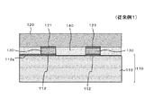
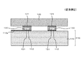
バンプを用いた従来技術において、LSIチップ−配線基板間がはんだバンプを介してフリップチップ接続される場合、弾性率が高いはんだバンプは、LSIチップ−配線基板間の熱膨張差により高い応力が発生し、はんだバンプ自身又ははんだバンプ近傍のLSIチップにおけるLSI回路を破壊するおそれがある。特に、ハイエンド向け大型ASIC(Application Specific Integrated Circuit)を中心にLSIチップにおける絶縁層のLow−k(低誘電率)化によるLSI回路の脆弱化が進行しており、特に、応力によるLSI回路の破壊が顕著になっている。
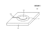
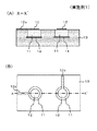
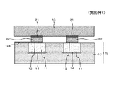
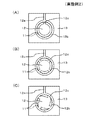
11 低弾性樹脂
12、112 実装パッド(パッド)
12a、112a 配線
12b 外周部
12c 結線部
13、113 絶縁層(基板)
13a 穴
14 金属層
20、120 半導体チップ(LSIチップ)
21、121 電極
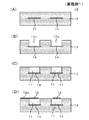
30、130 バンプ(金属層)
131 樹脂コア
140 アンダーフィル樹脂
さらに、以下の形態も可能である。
前記絶縁層中に配設されるとともに、少なくとも前記凹部の底面に配された金属層を備えることが好ましい。
前記絶縁層上に形成されるとともに、前記外周部と接続された配線を備えることが好ましい。
前記結線部は、直線状、曲線状、斜線状、又はこれらの組合せで形成されていることが好ましい。
前記配線基板と、前記配線基板のパッドと対応する位置に電極を有する半導体チップ又は半導体パッケージと、前記パッドと前記電極の間に配設されるとともに、前記パッドと前記電極を電気的に接続するバンプと、を備える半導体装置とすることが好ましい。
Claims (5)
- 所定の位置に凹部を有する絶縁層と、
前記凹部内に埋め込まれるとともに、前記絶縁層よりも低弾性な低弾性樹脂と、
前記低弾性樹脂上に配設されるとともに、前記低弾性樹脂の領域よりも小さい領域のパッドと、
を備え、
前記低弾性樹脂の領域の外周の前記絶縁層上に配設されるとともに、前記パッドと同一材料よりなる外周部と、
前記低弾性樹脂の領域内であって前記実装パッドと前記外周部の間の領域の一部に配設されるとともに、前記パッドと同一材料よりなり、かつ、前記実装パッドと前記外周部を結線する1又は複数の結線部と、
を備えることを特徴とする配線基板。 - 前記絶縁層中に配設されるとともに、少なくとも前記凹部の底面に配された金属層を備えることを特徴とする請求項1記載の配線基板。
- 前記絶縁層上に形成されるとともに、前記外周部と接続された配線を備えることを特徴とする請求項1又は2記載の配線基板。
- 前記結線部は、直線状、曲線状、斜線状、又はこれらの組合せで形成されていることを特徴とする請求項1乃至3のいずれか一に記載の配線基板。
- 請求項1乃至4のいずれか一に記載の配線基板と、
前記配線基板のパッドと対応する位置に電極を有する半導体チップ又は半導体パッケージと、
前記パッドと前記電極の間に配設されるとともに、前記パッドと前記電極を電気的に接続するバンプと、
を備えることを特徴とする半導体装置。
Priority Applications (1)
| Application Number | Priority Date | Filing Date | Title |
|---|---|---|---|
| JP2009554362A JP5515744B2 (ja) | 2008-02-21 | 2009-02-19 | 配線基板及び半導体装置 |
Applications Claiming Priority (4)
| Application Number | Priority Date | Filing Date | Title |
|---|---|---|---|
| JP2008040335 | 2008-02-21 | ||
| JP2008040335 | 2008-02-21 | ||
| JP2009554362A JP5515744B2 (ja) | 2008-02-21 | 2009-02-19 | 配線基板及び半導体装置 |
| PCT/JP2009/052862 WO2009104668A1 (ja) | 2008-02-21 | 2009-02-19 | 配線基板及び半導体装置 |
Publications (2)
| Publication Number | Publication Date |
|---|---|
| JPWO2009104668A1 JPWO2009104668A1 (ja) | 2011-06-23 |
| JP5515744B2 true JP5515744B2 (ja) | 2014-06-11 |
Family
ID=40985546
Family Applications (1)
| Application Number | Title | Priority Date | Filing Date |
|---|---|---|---|
| JP2009554362A Expired - Fee Related JP5515744B2 (ja) | 2008-02-21 | 2009-02-19 | 配線基板及び半導体装置 |
Country Status (2)
| Country | Link |
|---|---|
| JP (1) | JP5515744B2 (ja) |
| WO (1) | WO2009104668A1 (ja) |
Families Citing this family (13)
| Publication number | Priority date | Publication date | Assignee | Title |
|---|---|---|---|---|
| US8569876B2 (en) | 2006-11-22 | 2013-10-29 | Tessera, Inc. | Packaged semiconductor chips with array |
| JP5584474B2 (ja) | 2007-03-05 | 2014-09-03 | インヴェンサス・コーポレイション | 貫通ビアによって前面接点に接続された後面接点を有するチップ |
| CN103178032B (zh) | 2007-07-31 | 2017-06-20 | 英闻萨斯有限公司 | 使用穿透硅通道的半导体封装方法 |
| US8796135B2 (en) | 2010-07-23 | 2014-08-05 | Tessera, Inc. | Microelectronic elements with rear contacts connected with via first or via middle structures |
| US9640437B2 (en) | 2010-07-23 | 2017-05-02 | Tessera, Inc. | Methods of forming semiconductor elements using micro-abrasive particle stream |
| US8791575B2 (en) | 2010-07-23 | 2014-07-29 | Tessera, Inc. | Microelectronic elements having metallic pads overlying vias |
| US8847380B2 (en) | 2010-09-17 | 2014-09-30 | Tessera, Inc. | Staged via formation from both sides of chip |
| US8610259B2 (en) | 2010-09-17 | 2013-12-17 | Tessera, Inc. | Multi-function and shielded 3D interconnects |
| US8736066B2 (en) | 2010-12-02 | 2014-05-27 | Tessera, Inc. | Stacked microelectronic assemby with TSVS formed in stages and carrier above chip |
| US8587126B2 (en) | 2010-12-02 | 2013-11-19 | Tessera, Inc. | Stacked microelectronic assembly with TSVs formed in stages with plural active chips |
| US8637968B2 (en) | 2010-12-02 | 2014-01-28 | Tessera, Inc. | Stacked microelectronic assembly having interposer connecting active chips |
| US8610264B2 (en) | 2010-12-08 | 2013-12-17 | Tessera, Inc. | Compliant interconnects in wafers |
| DE102011014584A1 (de) * | 2011-03-21 | 2012-09-27 | Osram Opto Semiconductors Gmbh | Anschlussträger für Halbleiterchips und Halbleiterbauelement |
Citations (4)
| Publication number | Priority date | Publication date | Assignee | Title |
|---|---|---|---|---|
| JP2000277923A (ja) * | 1999-03-29 | 2000-10-06 | Nec Corp | マザーボードプリント配線板およびその製造方法 |
| JP2001094227A (ja) * | 1999-09-20 | 2001-04-06 | Shinko Electric Ind Co Ltd | 半導体チップ実装用の配線基板と該基板を用いた半導体チップの実装方法 |
| JP2003198068A (ja) * | 2001-12-27 | 2003-07-11 | Nec Corp | プリント基板、半導体装置、およびプリント基板と部品との電気的接続構造 |
| JP2004247549A (ja) * | 2003-02-14 | 2004-09-02 | Fujitsu Ltd | 配線基板の作製方法および多層配線基板の作製方法 |
-
2009
- 2009-02-19 JP JP2009554362A patent/JP5515744B2/ja not_active Expired - Fee Related
- 2009-02-19 WO PCT/JP2009/052862 patent/WO2009104668A1/ja not_active Ceased
Patent Citations (4)
| Publication number | Priority date | Publication date | Assignee | Title |
|---|---|---|---|---|
| JP2000277923A (ja) * | 1999-03-29 | 2000-10-06 | Nec Corp | マザーボードプリント配線板およびその製造方法 |
| JP2001094227A (ja) * | 1999-09-20 | 2001-04-06 | Shinko Electric Ind Co Ltd | 半導体チップ実装用の配線基板と該基板を用いた半導体チップの実装方法 |
| JP2003198068A (ja) * | 2001-12-27 | 2003-07-11 | Nec Corp | プリント基板、半導体装置、およびプリント基板と部品との電気的接続構造 |
| JP2004247549A (ja) * | 2003-02-14 | 2004-09-02 | Fujitsu Ltd | 配線基板の作製方法および多層配線基板の作製方法 |
Also Published As
| Publication number | Publication date |
|---|---|
| JPWO2009104668A1 (ja) | 2011-06-23 |
| WO2009104668A1 (ja) | 2009-08-27 |
Similar Documents
| Publication | Publication Date | Title |
|---|---|---|
| JP5515744B2 (ja) | 配線基板及び半導体装置 | |
| CN101226920B (zh) | 使用具有降低布线断开的布线结构的布线衬底的半导体器件 | |
| KR101376264B1 (ko) | 적층형 패키지 및 그 제조 방법 | |
| US8378482B2 (en) | Wiring board | |
| CN103000591B (zh) | 芯片封装件的环结构 | |
| JP2008071953A (ja) | 半導体装置 | |
| JP2001177010A (ja) | 配線基板、配線基板を有する半導体装置、及び、その製造方法、実装方法 | |
| JP2003051568A (ja) | 半導体装置 | |
| CN106471612A (zh) | 半导体器件及其制造方法 | |
| JP2009064812A (ja) | 半導体装置の電極構造およびその関連技術 | |
| US20120205802A1 (en) | Printed circuit board and flip chip package using the same with improved bump joint reliability | |
| CN106463472A (zh) | 半导体器件及制造其的方法 | |
| JP5015065B2 (ja) | 配線基板 | |
| CN106463427B (zh) | 半导体装置及其制造方法 | |
| JP2005129663A (ja) | 多層配線基板 | |
| JP4899406B2 (ja) | フリップチップ型半導体装置 | |
| JP4449608B2 (ja) | 半導体装置 | |
| JP2004128290A (ja) | 半導体装置 | |
| JP5375186B2 (ja) | 配線基板、配線基板の製造方法及び半導体装置実装構造 | |
| JP4521415B2 (ja) | 半導体装置 | |
| JP6464762B2 (ja) | 半導体パッケージ基板、および半導体パッケージと、半導体パッケージ基板の製造方法、および半導体パッケージの製造方法 | |
| JP4321269B2 (ja) | 半導体装置 | |
| JP2004128364A (ja) | 半導体パッケージおよび半導体パッケージの実装構造体 | |
| JP5434306B2 (ja) | 半導体装置及び半導体装置の製造方法 | |
| JP2007250712A (ja) | 半導体装置及びその製造方法 |
Legal Events
| Date | Code | Title | Description |
|---|---|---|---|
| A621 | Written request for application examination |
Free format text: JAPANESE INTERMEDIATE CODE: A621 Effective date: 20120112 |
|
| A131 | Notification of reasons for refusal |
Free format text: JAPANESE INTERMEDIATE CODE: A131 Effective date: 20131210 |
|
| A521 | Request for written amendment filed |
Free format text: JAPANESE INTERMEDIATE CODE: A523 Effective date: 20140210 |
|
| TRDD | Decision of grant or rejection written | ||
| A01 | Written decision to grant a patent or to grant a registration (utility model) |
Free format text: JAPANESE INTERMEDIATE CODE: A01 Effective date: 20140304 |
|
| A61 | First payment of annual fees (during grant procedure) |
Free format text: JAPANESE INTERMEDIATE CODE: A61 Effective date: 20140317 |
|
| R150 | Certificate of patent or registration of utility model |
Ref document number: 5515744 Country of ref document: JP Free format text: JAPANESE INTERMEDIATE CODE: R150 |
|
| LAPS | Cancellation because of no payment of annual fees |