JP4937842B2 - 半導体装置およびその製造方法 - Google Patents
半導体装置およびその製造方法 Download PDFInfo
- Publication number
- JP4937842B2 JP4937842B2 JP2007150289A JP2007150289A JP4937842B2 JP 4937842 B2 JP4937842 B2 JP 4937842B2 JP 2007150289 A JP2007150289 A JP 2007150289A JP 2007150289 A JP2007150289 A JP 2007150289A JP 4937842 B2 JP4937842 B2 JP 4937842B2
- Authority
- JP
- Japan
- Prior art keywords
- hole
- insulating film
- semiconductor
- semiconductor substrate
- pad
- Prior art date
- Legal status (The legal status is an assumption and is not a legal conclusion. Google has not performed a legal analysis and makes no representation as to the accuracy of the status listed.)
- Expired - Fee Related
Links
- 239000004065 semiconductor Substances 0.000 title claims abstract description 562
- 238000004519 manufacturing process Methods 0.000 title claims description 78
- 239000000758 substrate Substances 0.000 claims abstract description 253
- 239000011229 interlayer Substances 0.000 claims abstract description 219
- 238000005530 etching Methods 0.000 claims description 86
- 238000000034 method Methods 0.000 claims description 83
- 239000004020 conductor Substances 0.000 claims description 49
- 230000008569 process Effects 0.000 claims description 35
- 238000012545 processing Methods 0.000 claims description 27
- 238000000059 patterning Methods 0.000 claims description 18
- 230000000873 masking effect Effects 0.000 claims description 3
- 229910052710 silicon Inorganic materials 0.000 abstract description 44
- 239000010703 silicon Substances 0.000 abstract description 44
- 230000035515 penetration Effects 0.000 abstract description 5
- XUIMIQQOPSSXEZ-UHFFFAOYSA-N Silicon Chemical compound [Si] XUIMIQQOPSSXEZ-UHFFFAOYSA-N 0.000 description 42
- 239000010410 layer Substances 0.000 description 24
- 238000007747 plating Methods 0.000 description 15
- 229910052782 aluminium Inorganic materials 0.000 description 14
- XAGFODPZIPBFFR-UHFFFAOYSA-N aluminium Chemical compound [Al] XAGFODPZIPBFFR-UHFFFAOYSA-N 0.000 description 14
- 239000010931 gold Substances 0.000 description 13
- VYPSYNLAJGMNEJ-UHFFFAOYSA-N Silicium dioxide Chemical compound O=[Si]=O VYPSYNLAJGMNEJ-UHFFFAOYSA-N 0.000 description 12
- 230000015572 biosynthetic process Effects 0.000 description 12
- PCHJSUWPFVWCPO-UHFFFAOYSA-N gold Chemical compound [Au] PCHJSUWPFVWCPO-UHFFFAOYSA-N 0.000 description 12
- 229910052737 gold Inorganic materials 0.000 description 12
- 230000007423 decrease Effects 0.000 description 11
- 229910052814 silicon oxide Inorganic materials 0.000 description 11
- 238000000206 photolithography Methods 0.000 description 8
- 239000010936 titanium Substances 0.000 description 8
- RTAQQCXQSZGOHL-UHFFFAOYSA-N Titanium Chemical compound [Ti] RTAQQCXQSZGOHL-UHFFFAOYSA-N 0.000 description 7
- 230000008901 benefit Effects 0.000 description 7
- 230000000694 effects Effects 0.000 description 7
- 229910000679 solder Inorganic materials 0.000 description 7
- 239000000243 solution Substances 0.000 description 7
- 229910052719 titanium Inorganic materials 0.000 description 7
- 238000009413 insulation Methods 0.000 description 6
- 238000000227 grinding Methods 0.000 description 5
- 230000009467 reduction Effects 0.000 description 5
- KRHYYFGTRYWZRS-UHFFFAOYSA-N Fluorane Chemical compound F KRHYYFGTRYWZRS-UHFFFAOYSA-N 0.000 description 4
- 239000012790 adhesive layer Substances 0.000 description 4
- 230000007547 defect Effects 0.000 description 4
- 238000010586 diagram Methods 0.000 description 4
- 239000007789 gas Substances 0.000 description 4
- 230000001965 increasing effect Effects 0.000 description 4
- 238000001459 lithography Methods 0.000 description 4
- 230000000149 penetrating effect Effects 0.000 description 4
- 238000005498 polishing Methods 0.000 description 4
- 238000009713 electroplating Methods 0.000 description 3
- 238000010438 heat treatment Methods 0.000 description 3
- 229910052751 metal Inorganic materials 0.000 description 3
- 239000002184 metal Substances 0.000 description 3
- 230000004048 modification Effects 0.000 description 3
- 238000012986 modification Methods 0.000 description 3
- 239000012945 sealing adhesive Substances 0.000 description 3
- 238000004544 sputter deposition Methods 0.000 description 3
- NBIIXXVUZAFLBC-UHFFFAOYSA-N Phosphoric acid Chemical compound OP(O)(O)=O NBIIXXVUZAFLBC-UHFFFAOYSA-N 0.000 description 2
- 238000004380 ashing Methods 0.000 description 2
- QVGXLLKOCUKJST-UHFFFAOYSA-N atomic oxygen Chemical compound [O] QVGXLLKOCUKJST-UHFFFAOYSA-N 0.000 description 2
- 238000005229 chemical vapour deposition Methods 0.000 description 2
- 239000011651 chromium Substances 0.000 description 2
- 238000004140 cleaning Methods 0.000 description 2
- 238000000576 coating method Methods 0.000 description 2
- 239000010949 copper Substances 0.000 description 2
- 238000001312 dry etching Methods 0.000 description 2
- 238000007772 electroless plating Methods 0.000 description 2
- 238000005516 engineering process Methods 0.000 description 2
- 230000004927 fusion Effects 0.000 description 2
- 239000007769 metal material Substances 0.000 description 2
- 239000003960 organic solvent Substances 0.000 description 2
- 239000001301 oxygen Substances 0.000 description 2
- 229910052760 oxygen Inorganic materials 0.000 description 2
- 238000005507 spraying Methods 0.000 description 2
- 238000007740 vapor deposition Methods 0.000 description 2
- XZXYQEHISUMZAT-UHFFFAOYSA-N 2-[(2-hydroxy-5-methylphenyl)methyl]-4-methylphenol Chemical compound CC1=CC=C(O)C(CC=2C(=CC=C(C)C=2)O)=C1 XZXYQEHISUMZAT-UHFFFAOYSA-N 0.000 description 1
- ZCYVEMRRCGMTRW-UHFFFAOYSA-N 7553-56-2 Chemical compound [I] ZCYVEMRRCGMTRW-UHFFFAOYSA-N 0.000 description 1
- VYZAMTAEIAYCRO-UHFFFAOYSA-N Chromium Chemical compound [Cr] VYZAMTAEIAYCRO-UHFFFAOYSA-N 0.000 description 1
- RYGMFSIKBFXOCR-UHFFFAOYSA-N Copper Chemical compound [Cu] RYGMFSIKBFXOCR-UHFFFAOYSA-N 0.000 description 1
- 229910052581 Si3N4 Inorganic materials 0.000 description 1
- NRTOMJZYCJJWKI-UHFFFAOYSA-N Titanium nitride Chemical compound [Ti]#N NRTOMJZYCJJWKI-UHFFFAOYSA-N 0.000 description 1
- 229910000147 aluminium phosphate Inorganic materials 0.000 description 1
- 229940107816 ammonium iodide Drugs 0.000 description 1
- 230000004888 barrier function Effects 0.000 description 1
- 230000005540 biological transmission Effects 0.000 description 1
- 229910052804 chromium Inorganic materials 0.000 description 1
- 239000000470 constituent Substances 0.000 description 1
- 229910052802 copper Inorganic materials 0.000 description 1
- 230000002950 deficient Effects 0.000 description 1
- 238000013461 design Methods 0.000 description 1
- 238000011161 development Methods 0.000 description 1
- 230000002708 enhancing effect Effects 0.000 description 1
- 230000005669 field effect Effects 0.000 description 1
- 239000007888 film coating Substances 0.000 description 1
- 238000009501 film coating Methods 0.000 description 1
- 239000011521 glass Substances 0.000 description 1
- 238000009616 inductively coupled plasma Methods 0.000 description 1
- 239000012212 insulator Substances 0.000 description 1
- 229910052740 iodine Inorganic materials 0.000 description 1
- 239000011630 iodine Substances 0.000 description 1
- 238000010030 laminating Methods 0.000 description 1
- 239000000463 material Substances 0.000 description 1
- 230000008018 melting Effects 0.000 description 1
- 238000002844 melting Methods 0.000 description 1
- 239000011259 mixed solution Substances 0.000 description 1
- 238000001020 plasma etching Methods 0.000 description 1
- 229920001721 polyimide Polymers 0.000 description 1
- 239000009719 polyimide resin Substances 0.000 description 1
- 239000010453 quartz Substances 0.000 description 1
- HQVNEWCFYHHQES-UHFFFAOYSA-N silicon nitride Chemical compound N12[Si]34N5[Si]62N3[Si]51N64 HQVNEWCFYHHQES-UHFFFAOYSA-N 0.000 description 1
- 239000002356 single layer Substances 0.000 description 1
- 239000000126 substance Substances 0.000 description 1
- 229920001169 thermoplastic Polymers 0.000 description 1
- 239000004416 thermosoftening plastic Substances 0.000 description 1
Images


Classifications
-
- H—ELECTRICITY
- H01—ELECTRIC ELEMENTS
- H01L—SEMICONDUCTOR DEVICES NOT COVERED BY CLASS H10
- H01L23/00—Details of semiconductor or other solid state devices
- H01L23/12—Mountings, e.g. non-detachable insulating substrates
-
- H—ELECTRICITY
- H01—ELECTRIC ELEMENTS
- H01L—SEMICONDUCTOR DEVICES NOT COVERED BY CLASS H10
- H01L21/00—Processes or apparatus adapted for the manufacture or treatment of semiconductor or solid state devices or of parts thereof
- H01L21/70—Manufacture or treatment of devices consisting of a plurality of solid state components formed in or on a common substrate or of parts thereof; Manufacture of integrated circuit devices or of parts thereof
- H01L21/71—Manufacture of specific parts of devices defined in group H01L21/70
- H01L21/768—Applying interconnections to be used for carrying current between separate components within a device comprising conductors and dielectrics
- H01L21/76898—Applying interconnections to be used for carrying current between separate components within a device comprising conductors and dielectrics formed through a semiconductor substrate
-
- H—ELECTRICITY
- H01—ELECTRIC ELEMENTS
- H01L—SEMICONDUCTOR DEVICES NOT COVERED BY CLASS H10
- H01L21/00—Processes or apparatus adapted for the manufacture or treatment of semiconductor or solid state devices or of parts thereof
- H01L21/67—Apparatus specially adapted for handling semiconductor or electric solid state devices during manufacture or treatment thereof; Apparatus specially adapted for handling wafers during manufacture or treatment of semiconductor or electric solid state devices or components ; Apparatus not specifically provided for elsewhere
- H01L21/683—Apparatus specially adapted for handling semiconductor or electric solid state devices during manufacture or treatment thereof; Apparatus specially adapted for handling wafers during manufacture or treatment of semiconductor or electric solid state devices or components ; Apparatus not specifically provided for elsewhere for supporting or gripping
- H01L21/6835—Apparatus specially adapted for handling semiconductor or electric solid state devices during manufacture or treatment thereof; Apparatus specially adapted for handling wafers during manufacture or treatment of semiconductor or electric solid state devices or components ; Apparatus not specifically provided for elsewhere for supporting or gripping using temporarily an auxiliary support
-
- H—ELECTRICITY
- H01—ELECTRIC ELEMENTS
- H01L—SEMICONDUCTOR DEVICES NOT COVERED BY CLASS H10
- H01L23/00—Details of semiconductor or other solid state devices
- H01L23/48—Arrangements for conducting electric current to or from the solid state body in operation, e.g. leads, terminal arrangements ; Selection of materials therefor
-
- H—ELECTRICITY
- H01—ELECTRIC ELEMENTS
- H01L—SEMICONDUCTOR DEVICES NOT COVERED BY CLASS H10
- H01L24/00—Arrangements for connecting or disconnecting semiconductor or solid-state bodies; Methods or apparatus related thereto
- H01L24/01—Means for bonding being attached to, or being formed on, the surface to be connected, e.g. chip-to-package, die-attach, "first-level" interconnects; Manufacturing methods related thereto
- H01L24/02—Bonding areas ; Manufacturing methods related thereto
- H01L24/04—Structure, shape, material or disposition of the bonding areas prior to the connecting process
- H01L24/05—Structure, shape, material or disposition of the bonding areas prior to the connecting process of an individual bonding area
-
- H—ELECTRICITY
- H01—ELECTRIC ELEMENTS
- H01L—SEMICONDUCTOR DEVICES NOT COVERED BY CLASS H10
- H01L25/00—Assemblies consisting of a plurality of individual semiconductor or other solid state devices ; Multistep manufacturing processes thereof
- H01L25/03—Assemblies consisting of a plurality of individual semiconductor or other solid state devices ; Multistep manufacturing processes thereof all the devices being of a type provided for in the same subgroup of groups H01L27/00 - H01L33/00, or in a single subclass of H10K, H10N, e.g. assemblies of rectifier diodes
- H01L25/04—Assemblies consisting of a plurality of individual semiconductor or other solid state devices ; Multistep manufacturing processes thereof all the devices being of a type provided for in the same subgroup of groups H01L27/00 - H01L33/00, or in a single subclass of H10K, H10N, e.g. assemblies of rectifier diodes the devices not having separate containers
- H01L25/065—Assemblies consisting of a plurality of individual semiconductor or other solid state devices ; Multistep manufacturing processes thereof all the devices being of a type provided for in the same subgroup of groups H01L27/00 - H01L33/00, or in a single subclass of H10K, H10N, e.g. assemblies of rectifier diodes the devices not having separate containers the devices being of a type provided for in group H01L27/00
- H01L25/0657—Stacked arrangements of devices
-
- H—ELECTRICITY
- H01—ELECTRIC ELEMENTS
- H01L—SEMICONDUCTOR DEVICES NOT COVERED BY CLASS H10
- H01L25/00—Assemblies consisting of a plurality of individual semiconductor or other solid state devices ; Multistep manufacturing processes thereof
- H01L25/50—Multistep manufacturing processes of assemblies consisting of devices, each device being of a type provided for in group H01L27/00 or H01L29/00
-
- H—ELECTRICITY
- H01—ELECTRIC ELEMENTS
- H01L—SEMICONDUCTOR DEVICES NOT COVERED BY CLASS H10
- H01L2221/00—Processes or apparatus adapted for the manufacture or treatment of semiconductor or solid state devices or of parts thereof covered by H01L21/00
- H01L2221/67—Apparatus for handling semiconductor or electric solid state devices during manufacture or treatment thereof; Apparatus for handling wafers during manufacture or treatment of semiconductor or electric solid state devices or components; Apparatus not specifically provided for elsewhere
- H01L2221/683—Apparatus for handling semiconductor or electric solid state devices during manufacture or treatment thereof; Apparatus for handling wafers during manufacture or treatment of semiconductor or electric solid state devices or components; Apparatus not specifically provided for elsewhere for supporting or gripping
- H01L2221/68304—Apparatus for handling semiconductor or electric solid state devices during manufacture or treatment thereof; Apparatus for handling wafers during manufacture or treatment of semiconductor or electric solid state devices or components; Apparatus not specifically provided for elsewhere for supporting or gripping using temporarily an auxiliary support
- H01L2221/68372—Apparatus for handling semiconductor or electric solid state devices during manufacture or treatment thereof; Apparatus for handling wafers during manufacture or treatment of semiconductor or electric solid state devices or components; Apparatus not specifically provided for elsewhere for supporting or gripping using temporarily an auxiliary support used to support a device or wafer when forming electrical connections thereto
-
- H—ELECTRICITY
- H01—ELECTRIC ELEMENTS
- H01L—SEMICONDUCTOR DEVICES NOT COVERED BY CLASS H10
- H01L2224/00—Indexing scheme for arrangements for connecting or disconnecting semiconductor or solid-state bodies and methods related thereto as covered by H01L24/00
- H01L2224/01—Means for bonding being attached to, or being formed on, the surface to be connected, e.g. chip-to-package, die-attach, "first-level" interconnects; Manufacturing methods related thereto
- H01L2224/02—Bonding areas; Manufacturing methods related thereto
- H01L2224/023—Redistribution layers [RDL] for bonding areas
-
- H—ELECTRICITY
- H01—ELECTRIC ELEMENTS
- H01L—SEMICONDUCTOR DEVICES NOT COVERED BY CLASS H10
- H01L2224/00—Indexing scheme for arrangements for connecting or disconnecting semiconductor or solid-state bodies and methods related thereto as covered by H01L24/00
- H01L2224/01—Means for bonding being attached to, or being formed on, the surface to be connected, e.g. chip-to-package, die-attach, "first-level" interconnects; Manufacturing methods related thereto
- H01L2224/02—Bonding areas; Manufacturing methods related thereto
- H01L2224/04—Structure, shape, material or disposition of the bonding areas prior to the connecting process
- H01L2224/0401—Bonding areas specifically adapted for bump connectors, e.g. under bump metallisation [UBM]
-
- H—ELECTRICITY
- H01—ELECTRIC ELEMENTS
- H01L—SEMICONDUCTOR DEVICES NOT COVERED BY CLASS H10
- H01L2224/00—Indexing scheme for arrangements for connecting or disconnecting semiconductor or solid-state bodies and methods related thereto as covered by H01L24/00
- H01L2224/01—Means for bonding being attached to, or being formed on, the surface to be connected, e.g. chip-to-package, die-attach, "first-level" interconnects; Manufacturing methods related thereto
- H01L2224/02—Bonding areas; Manufacturing methods related thereto
- H01L2224/04—Structure, shape, material or disposition of the bonding areas prior to the connecting process
- H01L2224/05—Structure, shape, material or disposition of the bonding areas prior to the connecting process of an individual bonding area
- H01L2224/05001—Internal layers
- H01L2224/0502—Disposition
- H01L2224/05025—Disposition the internal layer being disposed on a via connection of the semiconductor or solid-state body
-
- H—ELECTRICITY
- H01—ELECTRIC ELEMENTS
- H01L—SEMICONDUCTOR DEVICES NOT COVERED BY CLASS H10
- H01L2224/00—Indexing scheme for arrangements for connecting or disconnecting semiconductor or solid-state bodies and methods related thereto as covered by H01L24/00
- H01L2224/01—Means for bonding being attached to, or being formed on, the surface to be connected, e.g. chip-to-package, die-attach, "first-level" interconnects; Manufacturing methods related thereto
- H01L2224/02—Bonding areas; Manufacturing methods related thereto
- H01L2224/04—Structure, shape, material or disposition of the bonding areas prior to the connecting process
- H01L2224/05—Structure, shape, material or disposition of the bonding areas prior to the connecting process of an individual bonding area
- H01L2224/0554—External layer
- H01L2224/0555—Shape
- H01L2224/05552—Shape in top view
- H01L2224/05553—Shape in top view being rectangular
-
- H—ELECTRICITY
- H01—ELECTRIC ELEMENTS
- H01L—SEMICONDUCTOR DEVICES NOT COVERED BY CLASS H10
- H01L2224/00—Indexing scheme for arrangements for connecting or disconnecting semiconductor or solid-state bodies and methods related thereto as covered by H01L24/00
- H01L2224/01—Means for bonding being attached to, or being formed on, the surface to be connected, e.g. chip-to-package, die-attach, "first-level" interconnects; Manufacturing methods related thereto
- H01L2224/02—Bonding areas; Manufacturing methods related thereto
- H01L2224/04—Structure, shape, material or disposition of the bonding areas prior to the connecting process
- H01L2224/05—Structure, shape, material or disposition of the bonding areas prior to the connecting process of an individual bonding area
- H01L2224/0554—External layer
- H01L2224/0556—Disposition
- H01L2224/0557—Disposition the external layer being disposed on a via connection of the semiconductor or solid-state body
-
- H—ELECTRICITY
- H01—ELECTRIC ELEMENTS
- H01L—SEMICONDUCTOR DEVICES NOT COVERED BY CLASS H10
- H01L2224/00—Indexing scheme for arrangements for connecting or disconnecting semiconductor or solid-state bodies and methods related thereto as covered by H01L24/00
- H01L2224/01—Means for bonding being attached to, or being formed on, the surface to be connected, e.g. chip-to-package, die-attach, "first-level" interconnects; Manufacturing methods related thereto
- H01L2224/02—Bonding areas; Manufacturing methods related thereto
- H01L2224/04—Structure, shape, material or disposition of the bonding areas prior to the connecting process
- H01L2224/05—Structure, shape, material or disposition of the bonding areas prior to the connecting process of an individual bonding area
- H01L2224/0554—External layer
- H01L2224/0556—Disposition
- H01L2224/05571—Disposition the external layer being disposed in a recess of the surface
- H01L2224/05572—Disposition the external layer being disposed in a recess of the surface the external layer extending out of an opening
-
- H—ELECTRICITY
- H01—ELECTRIC ELEMENTS
- H01L—SEMICONDUCTOR DEVICES NOT COVERED BY CLASS H10
- H01L2224/00—Indexing scheme for arrangements for connecting or disconnecting semiconductor or solid-state bodies and methods related thereto as covered by H01L24/00
- H01L2224/01—Means for bonding being attached to, or being formed on, the surface to be connected, e.g. chip-to-package, die-attach, "first-level" interconnects; Manufacturing methods related thereto
- H01L2224/10—Bump connectors; Manufacturing methods related thereto
- H01L2224/11—Manufacturing methods
- H01L2224/113—Manufacturing methods by local deposition of the material of the bump connector
- H01L2224/1133—Manufacturing methods by local deposition of the material of the bump connector in solid form
- H01L2224/1134—Stud bumping, i.e. using a wire-bonding apparatus
-
- H—ELECTRICITY
- H01—ELECTRIC ELEMENTS
- H01L—SEMICONDUCTOR DEVICES NOT COVERED BY CLASS H10
- H01L2224/00—Indexing scheme for arrangements for connecting or disconnecting semiconductor or solid-state bodies and methods related thereto as covered by H01L24/00
- H01L2224/01—Means for bonding being attached to, or being formed on, the surface to be connected, e.g. chip-to-package, die-attach, "first-level" interconnects; Manufacturing methods related thereto
- H01L2224/10—Bump connectors; Manufacturing methods related thereto
- H01L2224/12—Structure, shape, material or disposition of the bump connectors prior to the connecting process
- H01L2224/13—Structure, shape, material or disposition of the bump connectors prior to the connecting process of an individual bump connector
- H01L2224/13001—Core members of the bump connector
- H01L2224/1302—Disposition
- H01L2224/13025—Disposition the bump connector being disposed on a via connection of the semiconductor or solid-state body
-
- H—ELECTRICITY
- H01—ELECTRIC ELEMENTS
- H01L—SEMICONDUCTOR DEVICES NOT COVERED BY CLASS H10
- H01L2224/00—Indexing scheme for arrangements for connecting or disconnecting semiconductor or solid-state bodies and methods related thereto as covered by H01L24/00
- H01L2224/01—Means for bonding being attached to, or being formed on, the surface to be connected, e.g. chip-to-package, die-attach, "first-level" interconnects; Manufacturing methods related thereto
- H01L2224/10—Bump connectors; Manufacturing methods related thereto
- H01L2224/12—Structure, shape, material or disposition of the bump connectors prior to the connecting process
- H01L2224/13—Structure, shape, material or disposition of the bump connectors prior to the connecting process of an individual bump connector
- H01L2224/13001—Core members of the bump connector
- H01L2224/13099—Material
-
- H—ELECTRICITY
- H01—ELECTRIC ELEMENTS
- H01L—SEMICONDUCTOR DEVICES NOT COVERED BY CLASS H10
- H01L2224/00—Indexing scheme for arrangements for connecting or disconnecting semiconductor or solid-state bodies and methods related thereto as covered by H01L24/00
- H01L2224/01—Means for bonding being attached to, or being formed on, the surface to be connected, e.g. chip-to-package, die-attach, "first-level" interconnects; Manufacturing methods related thereto
- H01L2224/10—Bump connectors; Manufacturing methods related thereto
- H01L2224/15—Structure, shape, material or disposition of the bump connectors after the connecting process
- H01L2224/16—Structure, shape, material or disposition of the bump connectors after the connecting process of an individual bump connector
- H01L2224/161—Disposition
- H01L2224/16135—Disposition the bump connector connecting between different semiconductor or solid-state bodies, i.e. chip-to-chip
- H01L2224/16145—Disposition the bump connector connecting between different semiconductor or solid-state bodies, i.e. chip-to-chip the bodies being stacked
- H01L2224/16147—Disposition the bump connector connecting between different semiconductor or solid-state bodies, i.e. chip-to-chip the bodies being stacked the bump connector connecting to a bonding area disposed in a recess of the surface
-
- H—ELECTRICITY
- H01—ELECTRIC ELEMENTS
- H01L—SEMICONDUCTOR DEVICES NOT COVERED BY CLASS H10
- H01L2224/00—Indexing scheme for arrangements for connecting or disconnecting semiconductor or solid-state bodies and methods related thereto as covered by H01L24/00
- H01L2224/01—Means for bonding being attached to, or being formed on, the surface to be connected, e.g. chip-to-package, die-attach, "first-level" interconnects; Manufacturing methods related thereto
- H01L2224/10—Bump connectors; Manufacturing methods related thereto
- H01L2224/15—Structure, shape, material or disposition of the bump connectors after the connecting process
- H01L2224/16—Structure, shape, material or disposition of the bump connectors after the connecting process of an individual bump connector
- H01L2224/161—Disposition
- H01L2224/16151—Disposition the bump connector connecting between a semiconductor or solid-state body and an item not being a semiconductor or solid-state body, e.g. chip-to-substrate, chip-to-passive
- H01L2224/16221—Disposition the bump connector connecting between a semiconductor or solid-state body and an item not being a semiconductor or solid-state body, e.g. chip-to-substrate, chip-to-passive the body and the item being stacked
- H01L2224/16225—Disposition the bump connector connecting between a semiconductor or solid-state body and an item not being a semiconductor or solid-state body, e.g. chip-to-substrate, chip-to-passive the body and the item being stacked the item being non-metallic, e.g. insulating substrate with or without metallisation
- H01L2224/16237—Disposition the bump connector connecting between a semiconductor or solid-state body and an item not being a semiconductor or solid-state body, e.g. chip-to-substrate, chip-to-passive the body and the item being stacked the item being non-metallic, e.g. insulating substrate with or without metallisation the bump connector connecting to a bonding area disposed in a recess of the surface of the item
-
- H—ELECTRICITY
- H01—ELECTRIC ELEMENTS
- H01L—SEMICONDUCTOR DEVICES NOT COVERED BY CLASS H10
- H01L2224/00—Indexing scheme for arrangements for connecting or disconnecting semiconductor or solid-state bodies and methods related thereto as covered by H01L24/00
- H01L2224/80—Methods for connecting semiconductor or other solid state bodies using means for bonding being attached to, or being formed on, the surface to be connected
- H01L2224/81—Methods for connecting semiconductor or other solid state bodies using means for bonding being attached to, or being formed on, the surface to be connected using a bump connector
- H01L2224/8112—Aligning
- H01L2224/81136—Aligning involving guiding structures, e.g. spacers or supporting members
- H01L2224/81138—Aligning involving guiding structures, e.g. spacers or supporting members the guiding structures being at least partially left in the finished device
- H01L2224/81141—Guiding structures both on and outside the body
-
- H—ELECTRICITY
- H01—ELECTRIC ELEMENTS
- H01L—SEMICONDUCTOR DEVICES NOT COVERED BY CLASS H10
- H01L2224/00—Indexing scheme for arrangements for connecting or disconnecting semiconductor or solid-state bodies and methods related thereto as covered by H01L24/00
- H01L2224/80—Methods for connecting semiconductor or other solid state bodies using means for bonding being attached to, or being formed on, the surface to be connected
- H01L2224/81—Methods for connecting semiconductor or other solid state bodies using means for bonding being attached to, or being formed on, the surface to be connected using a bump connector
- H01L2224/8119—Arrangement of the bump connectors prior to mounting
- H01L2224/81191—Arrangement of the bump connectors prior to mounting wherein the bump connectors are disposed only on the semiconductor or solid-state body
-
- H—ELECTRICITY
- H01—ELECTRIC ELEMENTS
- H01L—SEMICONDUCTOR DEVICES NOT COVERED BY CLASS H10
- H01L2224/00—Indexing scheme for arrangements for connecting or disconnecting semiconductor or solid-state bodies and methods related thereto as covered by H01L24/00
- H01L2224/90—Methods for connecting semiconductor or solid state bodies using means for bonding not being attached to, or not being formed on, the body surface to be connected, e.g. pressure contacts using springs or clips
-
- H—ELECTRICITY
- H01—ELECTRIC ELEMENTS
- H01L—SEMICONDUCTOR DEVICES NOT COVERED BY CLASS H10
- H01L2225/00—Details relating to assemblies covered by the group H01L25/00 but not provided for in its subgroups
- H01L2225/03—All the devices being of a type provided for in the same subgroup of groups H01L27/00 - H01L33/648 and H10K99/00
- H01L2225/04—All the devices being of a type provided for in the same subgroup of groups H01L27/00 - H01L33/648 and H10K99/00 the devices not having separate containers
- H01L2225/065—All the devices being of a type provided for in the same subgroup of groups H01L27/00 - H01L33/648 and H10K99/00 the devices not having separate containers the devices being of a type provided for in group H01L27/00
- H01L2225/06503—Stacked arrangements of devices
- H01L2225/06513—Bump or bump-like direct electrical connections between devices, e.g. flip-chip connection, solder bumps
-
- H—ELECTRICITY
- H01—ELECTRIC ELEMENTS
- H01L—SEMICONDUCTOR DEVICES NOT COVERED BY CLASS H10
- H01L2225/00—Details relating to assemblies covered by the group H01L25/00 but not provided for in its subgroups
- H01L2225/03—All the devices being of a type provided for in the same subgroup of groups H01L27/00 - H01L33/648 and H10K99/00
- H01L2225/04—All the devices being of a type provided for in the same subgroup of groups H01L27/00 - H01L33/648 and H10K99/00 the devices not having separate containers
- H01L2225/065—All the devices being of a type provided for in the same subgroup of groups H01L27/00 - H01L33/648 and H10K99/00 the devices not having separate containers the devices being of a type provided for in group H01L27/00
- H01L2225/06503—Stacked arrangements of devices
- H01L2225/06517—Bump or bump-like direct electrical connections from device to substrate
-
- H—ELECTRICITY
- H01—ELECTRIC ELEMENTS
- H01L—SEMICONDUCTOR DEVICES NOT COVERED BY CLASS H10
- H01L2225/00—Details relating to assemblies covered by the group H01L25/00 but not provided for in its subgroups
- H01L2225/03—All the devices being of a type provided for in the same subgroup of groups H01L27/00 - H01L33/648 and H10K99/00
- H01L2225/04—All the devices being of a type provided for in the same subgroup of groups H01L27/00 - H01L33/648 and H10K99/00 the devices not having separate containers
- H01L2225/065—All the devices being of a type provided for in the same subgroup of groups H01L27/00 - H01L33/648 and H10K99/00 the devices not having separate containers the devices being of a type provided for in group H01L27/00
- H01L2225/06503—Stacked arrangements of devices
- H01L2225/06541—Conductive via connections through the device, e.g. vertical interconnects, through silicon via [TSV]
-
- H—ELECTRICITY
- H01—ELECTRIC ELEMENTS
- H01L—SEMICONDUCTOR DEVICES NOT COVERED BY CLASS H10
- H01L24/00—Arrangements for connecting or disconnecting semiconductor or solid-state bodies; Methods or apparatus related thereto
- H01L24/90—Methods for connecting semiconductor or solid state bodies using means for bonding not being attached to, or not being formed on, the body surface to be connected, e.g. pressure contacts using springs or clips
-
- H—ELECTRICITY
- H01—ELECTRIC ELEMENTS
- H01L—SEMICONDUCTOR DEVICES NOT COVERED BY CLASS H10
- H01L2924/00—Indexing scheme for arrangements or methods for connecting or disconnecting semiconductor or solid-state bodies as covered by H01L24/00
- H01L2924/0001—Technical content checked by a classifier
- H01L2924/00013—Fully indexed content
-
- H—ELECTRICITY
- H01—ELECTRIC ELEMENTS
- H01L—SEMICONDUCTOR DEVICES NOT COVERED BY CLASS H10
- H01L2924/00—Indexing scheme for arrangements or methods for connecting or disconnecting semiconductor or solid-state bodies as covered by H01L24/00
- H01L2924/0001—Technical content checked by a classifier
- H01L2924/0002—Not covered by any one of groups H01L24/00, H01L24/00 and H01L2224/00
-
- H—ELECTRICITY
- H01—ELECTRIC ELEMENTS
- H01L—SEMICONDUCTOR DEVICES NOT COVERED BY CLASS H10
- H01L2924/00—Indexing scheme for arrangements or methods for connecting or disconnecting semiconductor or solid-state bodies as covered by H01L24/00
- H01L2924/01—Chemical elements
- H01L2924/01004—Beryllium [Be]
-
- H—ELECTRICITY
- H01—ELECTRIC ELEMENTS
- H01L—SEMICONDUCTOR DEVICES NOT COVERED BY CLASS H10
- H01L2924/00—Indexing scheme for arrangements or methods for connecting or disconnecting semiconductor or solid-state bodies as covered by H01L24/00
- H01L2924/01—Chemical elements
- H01L2924/01005—Boron [B]
-
- H—ELECTRICITY
- H01—ELECTRIC ELEMENTS
- H01L—SEMICONDUCTOR DEVICES NOT COVERED BY CLASS H10
- H01L2924/00—Indexing scheme for arrangements or methods for connecting or disconnecting semiconductor or solid-state bodies as covered by H01L24/00
- H01L2924/01—Chemical elements
- H01L2924/01006—Carbon [C]
-
- H—ELECTRICITY
- H01—ELECTRIC ELEMENTS
- H01L—SEMICONDUCTOR DEVICES NOT COVERED BY CLASS H10
- H01L2924/00—Indexing scheme for arrangements or methods for connecting or disconnecting semiconductor or solid-state bodies as covered by H01L24/00
- H01L2924/01—Chemical elements
- H01L2924/01013—Aluminum [Al]
-
- H—ELECTRICITY
- H01—ELECTRIC ELEMENTS
- H01L—SEMICONDUCTOR DEVICES NOT COVERED BY CLASS H10
- H01L2924/00—Indexing scheme for arrangements or methods for connecting or disconnecting semiconductor or solid-state bodies as covered by H01L24/00
- H01L2924/01—Chemical elements
- H01L2924/01014—Silicon [Si]
-
- H—ELECTRICITY
- H01—ELECTRIC ELEMENTS
- H01L—SEMICONDUCTOR DEVICES NOT COVERED BY CLASS H10
- H01L2924/00—Indexing scheme for arrangements or methods for connecting or disconnecting semiconductor or solid-state bodies as covered by H01L24/00
- H01L2924/01—Chemical elements
- H01L2924/01015—Phosphorus [P]
-
- H—ELECTRICITY
- H01—ELECTRIC ELEMENTS
- H01L—SEMICONDUCTOR DEVICES NOT COVERED BY CLASS H10
- H01L2924/00—Indexing scheme for arrangements or methods for connecting or disconnecting semiconductor or solid-state bodies as covered by H01L24/00
- H01L2924/01—Chemical elements
- H01L2924/01018—Argon [Ar]
-
- H—ELECTRICITY
- H01—ELECTRIC ELEMENTS
- H01L—SEMICONDUCTOR DEVICES NOT COVERED BY CLASS H10
- H01L2924/00—Indexing scheme for arrangements or methods for connecting or disconnecting semiconductor or solid-state bodies as covered by H01L24/00
- H01L2924/01—Chemical elements
- H01L2924/01019—Potassium [K]
-
- H—ELECTRICITY
- H01—ELECTRIC ELEMENTS
- H01L—SEMICONDUCTOR DEVICES NOT COVERED BY CLASS H10
- H01L2924/00—Indexing scheme for arrangements or methods for connecting or disconnecting semiconductor or solid-state bodies as covered by H01L24/00
- H01L2924/01—Chemical elements
- H01L2924/01022—Titanium [Ti]
-
- H—ELECTRICITY
- H01—ELECTRIC ELEMENTS
- H01L—SEMICONDUCTOR DEVICES NOT COVERED BY CLASS H10
- H01L2924/00—Indexing scheme for arrangements or methods for connecting or disconnecting semiconductor or solid-state bodies as covered by H01L24/00
- H01L2924/01—Chemical elements
- H01L2924/01024—Chromium [Cr]
-
- H—ELECTRICITY
- H01—ELECTRIC ELEMENTS
- H01L—SEMICONDUCTOR DEVICES NOT COVERED BY CLASS H10
- H01L2924/00—Indexing scheme for arrangements or methods for connecting or disconnecting semiconductor or solid-state bodies as covered by H01L24/00
- H01L2924/01—Chemical elements
- H01L2924/01029—Copper [Cu]
-
- H—ELECTRICITY
- H01—ELECTRIC ELEMENTS
- H01L—SEMICONDUCTOR DEVICES NOT COVERED BY CLASS H10
- H01L2924/00—Indexing scheme for arrangements or methods for connecting or disconnecting semiconductor or solid-state bodies as covered by H01L24/00
- H01L2924/01—Chemical elements
- H01L2924/01033—Arsenic [As]
-
- H—ELECTRICITY
- H01—ELECTRIC ELEMENTS
- H01L—SEMICONDUCTOR DEVICES NOT COVERED BY CLASS H10
- H01L2924/00—Indexing scheme for arrangements or methods for connecting or disconnecting semiconductor or solid-state bodies as covered by H01L24/00
- H01L2924/01—Chemical elements
- H01L2924/01047—Silver [Ag]
-
- H—ELECTRICITY
- H01—ELECTRIC ELEMENTS
- H01L—SEMICONDUCTOR DEVICES NOT COVERED BY CLASS H10
- H01L2924/00—Indexing scheme for arrangements or methods for connecting or disconnecting semiconductor or solid-state bodies as covered by H01L24/00
- H01L2924/01—Chemical elements
- H01L2924/01078—Platinum [Pt]
-
- H—ELECTRICITY
- H01—ELECTRIC ELEMENTS
- H01L—SEMICONDUCTOR DEVICES NOT COVERED BY CLASS H10
- H01L2924/00—Indexing scheme for arrangements or methods for connecting or disconnecting semiconductor or solid-state bodies as covered by H01L24/00
- H01L2924/01—Chemical elements
- H01L2924/01079—Gold [Au]
-
- H—ELECTRICITY
- H01—ELECTRIC ELEMENTS
- H01L—SEMICONDUCTOR DEVICES NOT COVERED BY CLASS H10
- H01L2924/00—Indexing scheme for arrangements or methods for connecting or disconnecting semiconductor or solid-state bodies as covered by H01L24/00
- H01L2924/01—Chemical elements
- H01L2924/01082—Lead [Pb]
-
- H—ELECTRICITY
- H01—ELECTRIC ELEMENTS
- H01L—SEMICONDUCTOR DEVICES NOT COVERED BY CLASS H10
- H01L2924/00—Indexing scheme for arrangements or methods for connecting or disconnecting semiconductor or solid-state bodies as covered by H01L24/00
- H01L2924/013—Alloys
- H01L2924/014—Solder alloys
-
- H—ELECTRICITY
- H01—ELECTRIC ELEMENTS
- H01L—SEMICONDUCTOR DEVICES NOT COVERED BY CLASS H10
- H01L2924/00—Indexing scheme for arrangements or methods for connecting or disconnecting semiconductor or solid-state bodies as covered by H01L24/00
- H01L2924/049—Nitrides composed of metals from groups of the periodic table
- H01L2924/0494—4th Group
- H01L2924/04941—TiN
-
- H—ELECTRICITY
- H01—ELECTRIC ELEMENTS
- H01L—SEMICONDUCTOR DEVICES NOT COVERED BY CLASS H10
- H01L2924/00—Indexing scheme for arrangements or methods for connecting or disconnecting semiconductor or solid-state bodies as covered by H01L24/00
- H01L2924/049—Nitrides composed of metals from groups of the periodic table
- H01L2924/0504—14th Group
- H01L2924/05042—Si3N4
-
- H—ELECTRICITY
- H01—ELECTRIC ELEMENTS
- H01L—SEMICONDUCTOR DEVICES NOT COVERED BY CLASS H10
- H01L2924/00—Indexing scheme for arrangements or methods for connecting or disconnecting semiconductor or solid-state bodies as covered by H01L24/00
- H01L2924/10—Details of semiconductor or other solid state devices to be connected
- H01L2924/11—Device type
- H01L2924/13—Discrete devices, e.g. 3 terminal devices
- H01L2924/1304—Transistor
- H01L2924/1306—Field-effect transistor [FET]
-
- H—ELECTRICITY
- H01—ELECTRIC ELEMENTS
- H01L—SEMICONDUCTOR DEVICES NOT COVERED BY CLASS H10
- H01L2924/00—Indexing scheme for arrangements or methods for connecting or disconnecting semiconductor or solid-state bodies as covered by H01L24/00
- H01L2924/10—Details of semiconductor or other solid state devices to be connected
- H01L2924/11—Device type
- H01L2924/14—Integrated circuits
-
- H—ELECTRICITY
- H01—ELECTRIC ELEMENTS
- H01L—SEMICONDUCTOR DEVICES NOT COVERED BY CLASS H10
- H01L2924/00—Indexing scheme for arrangements or methods for connecting or disconnecting semiconductor or solid-state bodies as covered by H01L24/00
- H01L2924/30—Technical effects
- H01L2924/301—Electrical effects
- H01L2924/30107—Inductance
Description
本実施の形態1では、マイコンチップのように高集積回路を搭載した半導体装置を例に挙げて図面を参照しながら説明する。
前記実施の形態1では、マイコンチップのように高集積回路を形成した半導体チップについて説明したが、本実施の形態2ではインターポーザチップのように再配線を行なうための半導体チップについて説明する。
前記実施の形態1では絶縁膜8を使用する例について説明しているが、本実施の形態3では絶縁膜8に代えて感光性絶縁膜を用いる例について説明する。以下に、本実施の形態3における半導体チップの製造方法について説明する。
本実施の形態4では、例えば、前記実施の形態1〜3で製造した半導体チップを3次元的に積層形成したSiP構造の半導体装置について説明する。
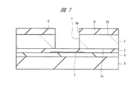
このように半導体チップ20aおよび半導体チップ20bをそれぞれ形成した後、積層することにより半導体装置を形成することができる。なお、半導体チップ20b上に半導体チップ20cを積層する場合も同様である。
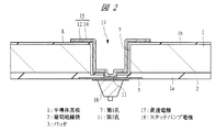
1a 第1面
1b 第2面
2 層間絶縁膜
3 パッド
4 接着層
5 支持基板
6 レジスト膜
6a 開口部
7 第1孔
8 絶縁膜
8a 感光性絶縁膜
9 アルミニウム膜
10 レジスト膜
10a 開口部
11 第2孔
12 シード層
13 レジスト膜
14 めっき膜
15 導体膜
16 レジスト膜
17 貫通電極
17a 貫通電極
17b 貫通電極
17c 貫通電極
18 スタッドバンプ電極
18a スタッドバンプ電極
18b スタッドバンプ電極
18c スタッドバンプ電極
19 クラック
20a 半導体チップ
20b 半導体チップ
20c 半導体チップ
21 配線基板
22 電極
23 半田バンプ電極
24 封止用接着材
Claims (20)
- (a)半導体基板の第1面に形成された半導体素子上に層間絶縁膜を形成し、前記層間絶縁膜の内部に形成された配線を介して前記半導体素子と電気的に接続するパッドを前記層間絶縁膜の表面に形成する工程と、
(b)前記半導体基板の前記第1面とは反対側にある第2面上に第1レジスト膜を形成する工程と、
(c)前記パッドと対向する位置に第1開口部を有するように前記第1レジスト膜をパターニングする工程と、
(d)前記第1開口部を形成した前記第1レジスト膜をマスクにして前記半導体基板をエッチングすることにより、底面に前記層間絶縁膜を露出する第1孔を前記半導体基板に形成する工程と、
(e)前記第1レジスト膜を除去する工程と、
(f)前記第1孔の底面に露出する前記層間絶縁膜をエッチングすることにより、前記第1孔の底面を前記層間絶縁膜上であって前記半導体基板と前記層間絶縁膜の境界よりも前記パッドに近い位置に形成する工程と、
(g)前記第1孔の内壁を含む前記半導体基板の前記第2面上に絶縁膜を形成する工程と、
(h)前記絶縁膜上に第2レジスト膜を形成する工程と、
(i)前記第1孔の底面に前記第1孔の径よりも小径の第2開口部を有するように前記第2レジスト膜をパターニングする工程と、
(j)前記第2開口部を形成した前記第2レジスト膜をマスクして前記絶縁膜および前記層間絶縁膜をエッチングすることにより、底面に前記パッドを露出する第2孔を形成する工程と、
(k)前記第1孔の内壁および前記第2孔の内壁を含む前記半導体基板の前記第2面に導体膜を形成し、前記導体膜をパターニングすることにより、前記半導体基板の前記第2面から前記第1面に達し、かつ、前記パッドに電気的に接続する貫通電極を形成する工程とを備え、
前記層間絶縁膜の前記半導体基板側の面は、前記第1孔の底面と前記半導体基板の前記第1面による段差を反映して段差形状になっており、
前記導体膜の表面は、前記半導体基板の前記第2面と前記第1孔の底面による段差を反映して段差形状になっていることを特徴とする半導体装置の製造方法。 - 請求項1記載の半導体装置の製造方法であって、
前記導体膜の表面は、前記半導体基板の前記第2面と前記第1孔の底面による段差および前記第1孔の底面と前記第2孔の底面による段差を反映して段差形状になっていることを特徴とする半導体装置の製造方法。 - 請求項1記載の半導体装置の製造方法であって、
前記(f)工程は、前記半導体基板に形成された前記第1孔をマスクにして前記第1孔の底面に露出する前記層間絶縁膜をエッチングすることを特徴とする半導体装置の製造方法。 - 請求項3記載の半導体装置の製造方法であって、
前記(f)工程では、新たなレジスト膜によるマスクを使用しない一方、前記(d)工程でのエッチングで使用するエッチングガスと前記(f)工程でのエッチングで使用するエッチングガスとは異なることを特徴とする半導体装置の製造方法。 - 請求項1記載の半導体装置の製造方法であって、
前記(d)工程後における前記第1孔の底面の径と、前記(f)工程後における前記第1孔の底面の径とは等しいことを特徴とする半導体装置の製造方法。 - 請求項1記載の半導体装置の製造方法であって、
前記(g)工程後、前記第1孔の底面と前記パッドとの間に残存する前記層間絶縁膜と前記第1孔の底面上に形成されている前記絶縁膜を合わせた膜厚は、前記(j)工程でマスクとして使用される前記第2レジスト膜が消失する前に前記第2孔が形成される膜厚であることを特徴とする半導体装置の製造方法。 - 請求項1記載の半導体装置の製造方法であって、
前記(c)工程は、赤外顕微鏡を用いて前記パッドと対向する位置に前記第1開口部を有するように前記第1レジスト膜をパターニングすることを特徴とする半導体装置の製造方法。 - 請求項1記載の半導体装置の製造方法であって、さらに、
(l)前記貫通電極と接続する側とは反対側の前記パッド上にバンプ電極を形成する工程とを備えることを特徴とする半導体装置の製造方法。 - 請求項1記載の半導体装置の製造方法であって、
前記貫通電極は、内部が空洞になっていることを特徴とする半導体装置の製造方法。 - 請求項1記載の半導体装置の製造方法であって、
(m)第1半導体ウェハにある個々のチップ領域に対して前記(a)工程から前記(k)工程までの処理を実施することにより前記第1半導体ウェハの個々のチップ領域に形成された第1パッドに電気的に接続する第1貫通電極を形成した後、前記第1貫通電極と接続する側とは反対側の前記第1パッド上に第1バンプ電極を形成する工程と、
(n)第2半導体ウェハにある個々のチップ領域に対して前記(a)工程から前記(k)工程までの処理を実施することにより前記第2半導体ウェハの個々のチップ領域に形成された第2パッドに電気的に接続する第2貫通電極を形成した後、前記第2貫通電極と接続する側とは反対側の前記第2パッド上に第2バンプ電極を形成する工程と、
(o)前記第1半導体ウェハ上に前記第2半導体ウェハを積層して電気的に接続する工程とを備え、
前記(o)工程は、前記第2半導体ウェハに形成されている前記第2バンプ電極を前記第1半導体ウェハに形成した前記第1貫通電極に圧接によって変形注入することにより、前記第1半導体ウェハと前記第2半導体ウェハとを電気的に接続することを特徴とする半導体装置の製造方法。 - 請求項1記載の半導体装置の製造方法であって、
(p)前記半導体基板として第1半導体ウェハを用い、前記第1半導体ウェハにある個々のチップ領域に対して前記(a)工程から前記(k)工程までの処理を実施することにより前記第1半導体ウェハの個々のチップ領域に形成された第1パッドに電気的に接続する第1貫通電極を形成した後、前記第1半導体ウェハを複数の半導体チップに個片化して第1半導体チップを取得する工程と、
(q)前記第1半導体チップにおいて、前記第1貫通電極と接続する側とは反対側の前記第1パッド上に第1バンプ電極を形成する工程と、
(r)前記半導体基板として第2半導体ウェハを用い、前記第2半導体ウェハにある個々のチップ領域に対して前記(a)工程から前記(k)工程までの処理を実施することにより前記第2半導体ウェハの個々のチップ領域に形成された第2パッドに電気的に接続する第2貫通電極を形成した後、前記第2半導体ウェハを複数の半導体チップに個片化して第2半導体チップを取得する工程と、
(s)前記第2半導体チップにおいて、前記第2貫通電極と接続する側とは反対側の前記第2パッド上に第2バンプ電極を形成する工程と、
(t)前記第1半導体チップ上に前記第2半導体チップを積層して電気的に接続する工程とを備え、
前記(t)工程は、前記第2半導体チップに形成されている前記第2バンプ電極を前記第1半導体チップに形成した前記第1貫通電極に圧接によって変形注入することにより、前記第1半導体チップと前記第2半導体チップとを電気的に接続することを特徴とする半導体装置の製造方法。 - (a)半導体基板の第1面に形成された半導体素子上に層間絶縁膜を形成し、前記層間絶縁膜の内部に形成された配線を介して前記半導体素子と電気的に接続するパッドを前記層間絶縁膜の表面に形成する工程と、
(b)前記半導体基板の前記第1面とは反対側にある第2面上に第1レジスト膜を形成する工程と、
(c)前記パッドと対向する位置に第1開口部を有するように前記第1レジスト膜をパターニングする工程と、
(d)前記第1開口部を形成した前記第1レジスト膜をマスクにして前記半導体基板をエッチングすることにより、底面に前記層間絶縁膜を露出する第1孔を前記半導体基板に形成する工程と、
(e)前記第1レジスト膜を除去する工程と、
(f)前記第1孔の底面に露出する前記層間絶縁膜をエッチングすることにより、前記第1孔の底面を前記層間絶縁膜上であって前記半導体基板と前記層間絶縁膜の境界よりも前記パッドに近い位置に形成する工程と、
(g)前記第1孔の内壁を含む前記半導体基板の前記第2面上に感光性絶縁膜を形成する工程と、
(h)前記第1孔の底面に前記第1孔の径よりも小径の第2開口部を有するように前記感光性絶縁膜をパターニングする工程と、
(i)前記第2開口部を形成した感光性絶縁膜をマスクして前記層間絶縁膜をエッチングすることにより、底面に前記パッドを露出する第2孔を形成する工程と、
(j)前記第1孔の内壁および前記第2孔の内壁を含む前記半導体基板の前記第2面に導体膜を形成し、前記導体膜をパターニングすることにより、前記半導体基板の前記第2面から前記第1面に達し、かつ、前記パッドに電気的に接続する貫通電極を形成する工程とを備え、
前記層間絶縁膜の前記半導体基板側の面は、前記第1孔の底面と前記半導体基板の前記第1面による段差を反映して段差形状になっており、
前記導体膜の表面は、前記半導体基板の前記第2面と前記第1孔の底面による段差を反映して段差形状になっていることを特徴とする半導体装置の製造方法。 - 請求項12記載の半導体装置の製造方法であって、
前記導体膜の表面は、前記半導体基板の前記第2面と前記第1孔の底面による段差および前記第1孔の底面と前記第2孔の底面による段差を反映して段差形状になっていることを特徴とする半導体装置の製造方法。 - 請求項12記載の半導体装置の製造方法であって、
前記(f)工程後、前記第1孔の底面と前記パッドとの間に残存する前記層間絶縁膜の膜厚は、前記(i)工程でマスクとして使用される前記感光性絶縁膜が消失する前に前記第2孔が形成される膜厚であることを特徴とする半導体装置の製造方法。 - 請求項12記載の半導体装置の製造方法であって、
前記貫通電極は、内部が空洞になっていることを特徴とする半導体装置の製造方法。 - (a)半導体基板と、
(b)前記半導体基板の第1面に形成された半導体素子と、
(c)前記半導体基板の前記第1面上に形成された層間絶縁膜と、
(d)前記層間絶縁膜上に形成されたパッドと、
(e)前記パッド上に形成されたバンプ電極と、
(f)前記半導体基板の前記第1面とは反対側にある第2面から前記パッドに達する貫通電極とを備え、
前記貫通電極は、
(f1)前記半導体基板の前記第1面とは反対側にある前記第2面から前記層間絶縁膜に達する第1孔であって、前記第1孔の底面が前記層間絶縁膜と前記半導体基板の境界よりも前記パッドに近い位置まで形成されている前記第1孔と、
(f2)前記第1孔の孔径よりも小さく、前記第1孔の底面から前記パッドに達するように形成された第2孔と、
(f3)前記第1孔の底面および側面と前記半導体基板の前記第2面上に形成された絶縁膜と、
(f4)前記第2孔の底面および側面と、前記絶縁膜を介した前記第1孔の底面および側面と前記半導体基板の前記第2面上に形成され、前記パッドと電気的に接続された導体膜とを有し、
前記層間絶縁膜の前記半導体基板側の面は、前記第1孔の底面と前記半導体基板の前記第1面による段差を反映して段差形状になっており、
前記導体膜の表面は、前記半導体基板の前記第2面と前記第1孔の底面による段差を反映して段差形状になっていることを特徴とする半導体装置。 - 請求項16記載の半導体装置であって、
前記導体膜の表面は、前記半導体基板の前記第2面と前記第1孔の底面による段差および前記第1孔の底面と前記第2孔の底面による段差を反映して段差形状になっていることを特徴とする半導体装置。 - 請求項16記載の半導体装置であって、
前記貫通電極は、内部が空洞となっていることを特徴とする半導体装置。 - 請求項16記載の半導体装置であって、
前記半導体基板の前記第2面側から前記貫通電極を見ると、平面的に、前記第1孔によるリングと前記第1孔よりも小さい前記第2孔によるリングにより2重リングになっていることを特徴とする半導体装置。 - 請求項16記載の半導体装置であって、
前記第2孔の底面である前記パッド上に形成されている前記導電膜の膜厚をaとし、前記第1孔の底面と前記パッド間に形成されている前記層間絶縁膜の膜厚および前記第1孔の底面上に形成されている前記絶縁膜の膜厚とを合わせた膜厚をbとするとき、a/(a+b)の値が0.11以上であることを特徴とする半導体装置。
Priority Applications (6)
| Application Number | Priority Date | Filing Date | Title |
|---|---|---|---|
| JP2007150289A JP4937842B2 (ja) | 2007-06-06 | 2007-06-06 | 半導体装置およびその製造方法 |
| TW097113552A TW200908152A (en) | 2007-06-06 | 2008-04-14 | Semiconductor device and manufacturing method thereof |
| CN2008101100054A CN101320702B (zh) | 2007-06-06 | 2008-06-02 | 半导体器件及其制造方法 |
| KR1020080052677A KR101191492B1 (ko) | 2007-06-06 | 2008-06-04 | 반도체 장치 및 그 제조 방법 |
| US12/133,828 US7973415B2 (en) | 2007-06-06 | 2008-06-05 | Manufacturing process and structure of through silicon via |
| US13/153,860 US8324736B2 (en) | 2007-06-06 | 2011-06-06 | Manufacturing process and structure of through silicon via |
Applications Claiming Priority (1)
| Application Number | Priority Date | Filing Date | Title |
|---|---|---|---|
| JP2007150289A JP4937842B2 (ja) | 2007-06-06 | 2007-06-06 | 半導体装置およびその製造方法 |
Related Child Applications (1)
| Application Number | Title | Priority Date | Filing Date |
|---|---|---|---|
| JP2012036709A Division JP2012134526A (ja) | 2012-02-22 | 2012-02-22 | 半導体装置 |
Publications (2)
| Publication Number | Publication Date |
|---|---|
| JP2008305897A JP2008305897A (ja) | 2008-12-18 |
| JP4937842B2 true JP4937842B2 (ja) | 2012-05-23 |
Family
ID=40180673
Family Applications (1)
| Application Number | Title | Priority Date | Filing Date |
|---|---|---|---|
| JP2007150289A Expired - Fee Related JP4937842B2 (ja) | 2007-06-06 | 2007-06-06 | 半導体装置およびその製造方法 |
Country Status (5)
| Country | Link |
|---|---|
| US (2) | US7973415B2 (ja) |
| JP (1) | JP4937842B2 (ja) |
| KR (1) | KR101191492B1 (ja) |
| CN (1) | CN101320702B (ja) |
| TW (1) | TW200908152A (ja) |
Families Citing this family (79)
| Publication number | Priority date | Publication date | Assignee | Title |
|---|---|---|---|---|
| US8569876B2 (en) | 2006-11-22 | 2013-10-29 | Tessera, Inc. | Packaged semiconductor chips with array |
| US7791199B2 (en) | 2006-11-22 | 2010-09-07 | Tessera, Inc. | Packaged semiconductor chips |
| CN101675516B (zh) | 2007-03-05 | 2012-06-20 | 数字光学欧洲有限公司 | 具有通过过孔连接到前侧触头的后侧触头的芯片 |
| JP2009021433A (ja) * | 2007-07-12 | 2009-01-29 | Fujikura Ltd | 配線基板及びその製造方法 |
| CN103178032B (zh) * | 2007-07-31 | 2017-06-20 | 英闻萨斯有限公司 | 使用穿透硅通道的半导体封装方法 |
| US20090212381A1 (en) * | 2008-02-26 | 2009-08-27 | Tessera, Inc. | Wafer level packages for rear-face illuminated solid state image sensors |
| US20100053407A1 (en) * | 2008-02-26 | 2010-03-04 | Tessera, Inc. | Wafer level compliant packages for rear-face illuminated solid state image sensors |
| TWI365528B (en) * | 2008-06-27 | 2012-06-01 | Advanced Semiconductor Eng | Semiconductor structure and method for manufacturing the same |
| KR100997788B1 (ko) * | 2008-06-30 | 2010-12-02 | 주식회사 하이닉스반도체 | 반도체 패키지 |
| US7872332B2 (en) | 2008-09-11 | 2011-01-18 | Micron Technology, Inc. | Interconnect structures for stacked dies, including penetrating structures for through-silicon vias, and associated systems and methods |
| JP2010080897A (ja) * | 2008-09-29 | 2010-04-08 | Panasonic Corp | 半導体装置及びその製造方法 |
| JP5455538B2 (ja) * | 2008-10-21 | 2014-03-26 | キヤノン株式会社 | 半導体装置及びその製造方法 |
| JP4803844B2 (ja) | 2008-10-21 | 2011-10-26 | インターナショナル・ビジネス・マシーンズ・コーポレーション | 半導体パッケージ |
| JP5434306B2 (ja) * | 2008-10-31 | 2014-03-05 | 日本電気株式会社 | 半導体装置及び半導体装置の製造方法 |
| DE102008058001A1 (de) * | 2008-11-19 | 2010-05-27 | Austriamicrosystems Ag | Verfahren zur Herstellung eines Halbleiterbauelementes und Halbleiterbauelement |
| US8513119B2 (en) | 2008-12-10 | 2013-08-20 | Taiwan Semiconductor Manufacturing Company, Ltd. | Method of forming bump structure having tapered sidewalls for stacked dies |
| US20100171197A1 (en) * | 2009-01-05 | 2010-07-08 | Hung-Pin Chang | Isolation Structure for Stacked Dies |
| US8198172B2 (en) * | 2009-02-25 | 2012-06-12 | Micron Technology, Inc. | Methods of forming integrated circuits using donor and acceptor substrates |
| JP5201048B2 (ja) * | 2009-03-25 | 2013-06-05 | 富士通株式会社 | 半導体装置とその製造方法 |
| TWI515869B (zh) * | 2009-07-30 | 2016-01-01 | 高通公司 | 系統級封裝 |
| US8791549B2 (en) | 2009-09-22 | 2014-07-29 | Taiwan Semiconductor Manufacturing Company, Ltd. | Wafer backside interconnect structure connected to TSVs |
| KR101096223B1 (ko) * | 2009-10-30 | 2011-12-22 | 주식회사 하이닉스반도체 | 단일측벽콘택에 연결된 매립비트라인을 갖는 반도체장치 제조 방법 |
| US8415238B2 (en) * | 2010-01-14 | 2013-04-09 | International Business Machines Corporation | Three dimensional integration and methods of through silicon via creation |
| US8399180B2 (en) * | 2010-01-14 | 2013-03-19 | International Business Machines Corporation | Three dimensional integration with through silicon vias having multiple diameters |
| US8304863B2 (en) * | 2010-02-09 | 2012-11-06 | International Business Machines Corporation | Electromigration immune through-substrate vias |
| US8541886B2 (en) * | 2010-03-09 | 2013-09-24 | Stats Chippac Ltd. | Integrated circuit packaging system with via and method of manufacture thereof |
| US8466059B2 (en) * | 2010-03-30 | 2013-06-18 | Taiwan Semiconductor Manufacturing Company, Ltd. | Multi-layer interconnect structure for stacked dies |
| US8324511B1 (en) | 2010-04-06 | 2012-12-04 | Amkor Technology, Inc. | Through via nub reveal method and structure |
| JP5423572B2 (ja) | 2010-05-07 | 2014-02-19 | セイコーエプソン株式会社 | 配線基板、圧電発振器、ジャイロセンサー、配線基板の製造方法 |
| US8202797B2 (en) | 2010-06-22 | 2012-06-19 | Stats Chippac Ltd. | Integrated circuit system with recessed through silicon via pads and method of manufacture thereof |
| US8796135B2 (en) | 2010-07-23 | 2014-08-05 | Tessera, Inc. | Microelectronic elements with rear contacts connected with via first or via middle structures |
| US8791575B2 (en) | 2010-07-23 | 2014-07-29 | Tessera, Inc. | Microelectronic elements having metallic pads overlying vias |
| US9640437B2 (en) | 2010-07-23 | 2017-05-02 | Tessera, Inc. | Methods of forming semiconductor elements using micro-abrasive particle stream |
| US8440554B1 (en) | 2010-08-02 | 2013-05-14 | Amkor Technology, Inc. | Through via connected backside embedded circuit features structure and method |
| JP2012064891A (ja) * | 2010-09-17 | 2012-03-29 | Toshiba Corp | 半導体装置及びその製造方法 |
| US8610259B2 (en) | 2010-09-17 | 2013-12-17 | Tessera, Inc. | Multi-function and shielded 3D interconnects |
| US8847380B2 (en) | 2010-09-17 | 2014-09-30 | Tessera, Inc. | Staged via formation from both sides of chip |
| US8487445B1 (en) | 2010-10-05 | 2013-07-16 | Amkor Technology, Inc. | Semiconductor device having through electrodes protruding from dielectric layer |
| KR101059490B1 (ko) | 2010-11-15 | 2011-08-25 | 테세라 리써치 엘엘씨 | 임베드된 트레이스에 의해 구성된 전도성 패드 |
| US8736066B2 (en) | 2010-12-02 | 2014-05-27 | Tessera, Inc. | Stacked microelectronic assemby with TSVS formed in stages and carrier above chip |
| US8587126B2 (en) | 2010-12-02 | 2013-11-19 | Tessera, Inc. | Stacked microelectronic assembly with TSVs formed in stages with plural active chips |
| US8637968B2 (en) | 2010-12-02 | 2014-01-28 | Tessera, Inc. | Stacked microelectronic assembly having interposer connecting active chips |
| US8610264B2 (en) | 2010-12-08 | 2013-12-17 | Tessera, Inc. | Compliant interconnects in wafers |
| US8390130B1 (en) | 2011-01-06 | 2013-03-05 | Amkor Technology, Inc. | Through via recessed reveal structure and method |
| US20120193809A1 (en) * | 2011-02-01 | 2012-08-02 | Nanya Technology Corp. | Integrated circuit device and method for preparing the same |
| JP5870493B2 (ja) | 2011-02-24 | 2016-03-01 | セイコーエプソン株式会社 | 半導体装置、センサーおよび電子デバイス |
| JP2012231096A (ja) * | 2011-04-27 | 2012-11-22 | Elpida Memory Inc | 半導体装置及びその製造方法 |
| US8900994B2 (en) | 2011-06-09 | 2014-12-02 | Taiwan Semiconductor Manufacturing Company, Ltd. | Method for producing a protective structure |
| US9076664B2 (en) | 2011-10-07 | 2015-07-07 | Freescale Semiconductor, Inc. | Stacked semiconductor die with continuous conductive vias |
| US8796822B2 (en) * | 2011-10-07 | 2014-08-05 | Freescale Semiconductor, Inc. | Stacked semiconductor devices |
| US8710670B2 (en) | 2011-12-14 | 2014-04-29 | Stats Chippac Ltd. | Integrated circuit packaging system with coupling features and method of manufacture thereof |
| JP5810921B2 (ja) * | 2012-01-06 | 2015-11-11 | 凸版印刷株式会社 | 半導体装置の製造方法 |
| CN103240481B (zh) * | 2012-02-08 | 2016-07-06 | 西安永电电气有限责任公司 | 焊接工装件 |
| US9780518B2 (en) | 2012-04-18 | 2017-10-03 | Cynosure, Inc. | Picosecond laser apparatus and methods for treating target tissues with same |
| CN103633013B (zh) * | 2012-08-21 | 2016-06-29 | 中芯国际集成电路制造(上海)有限公司 | 硅通孔封装结构的形成方法 |
| US20150187701A1 (en) | 2013-03-12 | 2015-07-02 | Taiwan Semiconductor Manufacturing Company, Ltd. | Semiconductor Devices and Methods of Manufacture Thereof |
| US9076715B2 (en) | 2013-03-12 | 2015-07-07 | Taiwan Semiconductor Manufacturing Company, Ltd. | Interconnect structure for connecting dies and methods of forming the same |
| JP5826782B2 (ja) * | 2013-03-19 | 2015-12-02 | 株式会社東芝 | 半導体装置の製造方法 |
| US9082757B2 (en) * | 2013-10-31 | 2015-07-14 | Freescale Semiconductor, Inc. | Stacked semiconductor devices |
| US9257641B2 (en) * | 2013-11-08 | 2016-02-09 | Industrial Technology Research Institute | Via structure, memory array structure, three-dimensional resistance memory and method of forming the same |
| US10056353B2 (en) | 2013-12-19 | 2018-08-21 | Taiwan Semiconductor Manufacturing Company, Ltd. | 3DIC interconnect apparatus and method |
| US9412719B2 (en) | 2013-12-19 | 2016-08-09 | Taiwan Semiconductor Manufacturing Company, Ltd. | 3DIC interconnect apparatus and method |
| US9425150B2 (en) | 2014-02-13 | 2016-08-23 | Taiwan Semiconductor Manufacturing Company, Ltd. | Multi-via interconnect structure and method of manufacture |
| US20150348874A1 (en) | 2014-05-29 | 2015-12-03 | Taiwan Semiconductor Manufacturing Company, Ltd. | 3DIC Interconnect Devices and Methods of Forming Same |
| US9543257B2 (en) | 2014-05-29 | 2017-01-10 | Taiwan Semiconductor Manufacturing Company, Ltd. | 3DIC interconnect devices and methods of forming same |
| US9455158B2 (en) | 2014-05-30 | 2016-09-27 | Taiwan Semiconductor Manufacturing Company, Ltd. | 3DIC interconnect devices and methods of forming same |
| US9449914B2 (en) | 2014-07-17 | 2016-09-20 | Taiwan Semiconductor Manufacturing Company, Ltd. | Stacked integrated circuits with redistribution lines |
| US9842825B2 (en) * | 2014-09-05 | 2017-12-12 | Taiwan Semiconductor Manufacturing Company, Ltd. | Substrateless integrated circuit packages and methods of forming same |
| US10002653B2 (en) | 2014-10-28 | 2018-06-19 | Nxp Usa, Inc. | Die stack address bus having a programmable width |
| DE112015006450T5 (de) * | 2015-04-14 | 2017-12-28 | Mitsubishi Electric Corporation | Halbleitereinheit |
| JP6648544B2 (ja) * | 2016-02-08 | 2020-02-14 | 三菱電機株式会社 | 半導体装置 |
| JP6443362B2 (ja) * | 2016-03-03 | 2018-12-26 | 株式会社デンソー | 半導体装置 |
| CN108257934B (zh) | 2016-12-29 | 2021-02-19 | 联华电子股份有限公司 | 焊垫开口及熔丝焊接口的制作方法与焊垫开口结构 |
| JP6888493B2 (ja) * | 2017-09-14 | 2021-06-16 | 三菱電機株式会社 | 半導体装置の製造方法 |
| CN107946239A (zh) * | 2017-12-06 | 2018-04-20 | 德淮半导体有限公司 | 硅通孔互连结构及其形成方法 |
| KR102576062B1 (ko) | 2018-11-07 | 2023-09-07 | 삼성전자주식회사 | 관통 실리콘 비아를 포함하는 반도체 소자 및 그 제조 방법 |
| CN111128872B (zh) * | 2019-12-30 | 2022-11-25 | 上海集成电路研发中心有限公司 | 一种接触孔及其制作方法 |
| US11393791B2 (en) * | 2020-01-28 | 2022-07-19 | Micron Technology, Inc. | Three-dimensional stacking semiconductor assemblies with near zero bond line thickness |
| TWI740716B (zh) * | 2020-11-16 | 2021-09-21 | 旭德科技股份有限公司 | 基板結構 |
Family Cites Families (19)
| Publication number | Priority date | Publication date | Assignee | Title |
|---|---|---|---|---|
| JP3724110B2 (ja) * | 1997-04-24 | 2005-12-07 | 三菱電機株式会社 | 半導体装置の製造方法 |
| JP3481444B2 (ja) | 1998-01-14 | 2003-12-22 | シャープ株式会社 | 半導体装置及びその製造方法 |
| JP3918350B2 (ja) | 1999-03-05 | 2007-05-23 | セイコーエプソン株式会社 | 半導体装置の製造方法 |
| JP3731453B2 (ja) * | 2000-07-07 | 2006-01-05 | セイコーエプソン株式会社 | 半導体装置の製造方法 |
| JP3910493B2 (ja) | 2002-06-14 | 2007-04-25 | 新光電気工業株式会社 | 半導体装置及びその製造方法 |
| JP2004296894A (ja) * | 2003-03-27 | 2004-10-21 | Seiko Epson Corp | 半導体装置の製造方法 |
| JP2005093486A (ja) * | 2003-09-12 | 2005-04-07 | Seiko Epson Corp | 半導体装置の製造方法及び半導体装置 |
| JP4441328B2 (ja) * | 2004-05-25 | 2010-03-31 | 株式会社ルネサステクノロジ | 半導体装置及びその製造方法 |
| KR100570514B1 (ko) | 2004-06-18 | 2006-04-13 | 삼성전자주식회사 | 웨이퍼 레벨 칩 스택 패키지 제조 방법 |
| JP4376715B2 (ja) * | 2004-07-16 | 2009-12-02 | 三洋電機株式会社 | 半導体装置の製造方法 |
| JP4373866B2 (ja) | 2004-07-16 | 2009-11-25 | 三洋電機株式会社 | 半導体装置の製造方法 |
| JP4365750B2 (ja) * | 2004-08-20 | 2009-11-18 | ローム株式会社 | 半導体チップの製造方法、および半導体装置の製造方法 |
| JP2006114545A (ja) * | 2004-10-12 | 2006-04-27 | Matsushita Electric Ind Co Ltd | 半導体装置およびその製造方法 |
| JP4547247B2 (ja) | 2004-12-17 | 2010-09-22 | ルネサスエレクトロニクス株式会社 | 半導体装置 |
| JP4409455B2 (ja) * | 2005-01-31 | 2010-02-03 | 株式会社ルネサステクノロジ | 半導体装置の製造方法 |
| JP2006222138A (ja) | 2005-02-08 | 2006-08-24 | Matsushita Electric Works Ltd | 貫通電極の形成方法 |
| JP4551255B2 (ja) | 2005-03-31 | 2010-09-22 | ルネサスエレクトロニクス株式会社 | 半導体装置 |
| JP4694305B2 (ja) * | 2005-08-16 | 2011-06-08 | ルネサスエレクトロニクス株式会社 | 半導体ウエハの製造方法 |
| JP4380718B2 (ja) * | 2007-03-15 | 2009-12-09 | ソニー株式会社 | 半導体装置の製造方法 |
-
2007
- 2007-06-06 JP JP2007150289A patent/JP4937842B2/ja not_active Expired - Fee Related
-
2008
- 2008-04-14 TW TW097113552A patent/TW200908152A/zh not_active IP Right Cessation
- 2008-06-02 CN CN2008101100054A patent/CN101320702B/zh not_active Expired - Fee Related
- 2008-06-04 KR KR1020080052677A patent/KR101191492B1/ko not_active IP Right Cessation
- 2008-06-05 US US12/133,828 patent/US7973415B2/en not_active Expired - Fee Related
-
2011
- 2011-06-06 US US13/153,860 patent/US8324736B2/en not_active Expired - Fee Related
Also Published As
| Publication number | Publication date |
|---|---|
| JP2008305897A (ja) | 2008-12-18 |
| KR101191492B1 (ko) | 2012-10-15 |
| CN101320702A (zh) | 2008-12-10 |
| CN101320702B (zh) | 2010-07-21 |
| US7973415B2 (en) | 2011-07-05 |
| US8324736B2 (en) | 2012-12-04 |
| TWI357111B (ja) | 2012-01-21 |
| KR20080107288A (ko) | 2008-12-10 |
| US20090014843A1 (en) | 2009-01-15 |
| US20110233773A1 (en) | 2011-09-29 |
| TW200908152A (en) | 2009-02-16 |
Similar Documents
| Publication | Publication Date | Title |
|---|---|---|
| JP4937842B2 (ja) | 半導体装置およびその製造方法 | |
| US8110900B2 (en) | Manufacturing process of semiconductor device and semiconductor device | |
| TWI505428B (zh) | 晶片封裝體及其形成方法 | |
| US9287172B2 (en) | Interposer-on-glass package method | |
| US9392705B2 (en) | Wiring board with through wiring | |
| US9196506B2 (en) | Method for manufacturing interposer | |
| JP4601686B2 (ja) | 半導体装置および半導体装置の製造方法 | |
| TW201611186A (zh) | 半導體裝置之製造方法 | |
| JP2005327984A (ja) | 電子部品及び電子部品実装構造の製造方法 | |
| JP2012069585A (ja) | 半導体装置およびその製造方法 | |
| KR20140005107A (ko) | 기판, 기판의 제조 방법, 반도체 장치, 및 전자 기기 | |
| KR101139650B1 (ko) | 배선 기판, 그 제조 방법, 및 반도체 장치 | |
| JP5775747B2 (ja) | 配線基板及びその製造方法 | |
| JP2008135553A (ja) | 基板積層方法及び基板が積層された半導体装置 | |
| JP5377657B2 (ja) | 半導体装置の製造方法 | |
| TWI544555B (zh) | 半導體封裝結構及其製造方法 | |
| JP2012134526A (ja) | 半導体装置 | |
| JP5006026B2 (ja) | 半導体装置 | |
| TWI470760B (zh) | 晶片封裝體及其形成方法 | |
| CN112997304A (zh) | 半导体装置 | |
| TWI459529B (zh) | 晶片封裝體及其形成方法 |
Legal Events
| Date | Code | Title | Description |
|---|---|---|---|
| A621 | Written request for application examination |
Free format text: JAPANESE INTERMEDIATE CODE: A621 Effective date: 20100212 |
|
| A711 | Notification of change in applicant |
Free format text: JAPANESE INTERMEDIATE CODE: A712 Effective date: 20100528 |
|
| A977 | Report on retrieval |
Free format text: JAPANESE INTERMEDIATE CODE: A971007 Effective date: 20120120 |
|
| TRDD | Decision of grant or rejection written | ||
| A01 | Written decision to grant a patent or to grant a registration (utility model) |
Free format text: JAPANESE INTERMEDIATE CODE: A01 Effective date: 20120124 |
|
| A01 | Written decision to grant a patent or to grant a registration (utility model) |
Free format text: JAPANESE INTERMEDIATE CODE: A01 |
|
| A61 | First payment of annual fees (during grant procedure) |
Free format text: JAPANESE INTERMEDIATE CODE: A61 Effective date: 20120222 |
|
| FPAY | Renewal fee payment (event date is renewal date of database) |
Free format text: PAYMENT UNTIL: 20150302 Year of fee payment: 3 |
|
| R150 | Certificate of patent or registration of utility model |
Free format text: JAPANESE INTERMEDIATE CODE: R150 |
|
| S531 | Written request for registration of change of domicile |
Free format text: JAPANESE INTERMEDIATE CODE: R313531 |
|
| R350 | Written notification of registration of transfer |
Free format text: JAPANESE INTERMEDIATE CODE: R350 |
|
| LAPS | Cancellation because of no payment of annual fees |