EP2264212A1 - Thin film deposition apparatus - Google Patents
Thin film deposition apparatus Download PDFInfo
- Publication number
- EP2264212A1 EP2264212A1 EP10250961A EP10250961A EP2264212A1 EP 2264212 A1 EP2264212 A1 EP 2264212A1 EP 10250961 A EP10250961 A EP 10250961A EP 10250961 A EP10250961 A EP 10250961A EP 2264212 A1 EP2264212 A1 EP 2264212A1
- Authority
- EP
- European Patent Office
- Prior art keywords
- nozzle
- substrate
- thin film
- deposition apparatus
- film deposition
- Prior art date
- Legal status (The legal status is an assumption and is not a legal conclusion. Google has not performed a legal analysis and makes no representation as to the accuracy of the status listed.)
- Granted
Links
Images








Classifications
-
- C—CHEMISTRY; METALLURGY
- C23—COATING METALLIC MATERIAL; COATING MATERIAL WITH METALLIC MATERIAL; CHEMICAL SURFACE TREATMENT; DIFFUSION TREATMENT OF METALLIC MATERIAL; COATING BY VACUUM EVAPORATION, BY SPUTTERING, BY ION IMPLANTATION OR BY CHEMICAL VAPOUR DEPOSITION, IN GENERAL; INHIBITING CORROSION OF METALLIC MATERIAL OR INCRUSTATION IN GENERAL
- C23C—COATING METALLIC MATERIAL; COATING MATERIAL WITH METALLIC MATERIAL; SURFACE TREATMENT OF METALLIC MATERIAL BY DIFFUSION INTO THE SURFACE, BY CHEMICAL CONVERSION OR SUBSTITUTION; COATING BY VACUUM EVAPORATION, BY SPUTTERING, BY ION IMPLANTATION OR BY CHEMICAL VAPOUR DEPOSITION, IN GENERAL
- C23C14/00—Coating by vacuum evaporation, by sputtering or by ion implantation of the coating forming material
- C23C14/22—Coating by vacuum evaporation, by sputtering or by ion implantation of the coating forming material characterised by the process of coating
- C23C14/24—Vacuum evaporation
Definitions
- the present invention relates to a thin film deposition apparatus, and more particularly to a thin film deposition apparatus that can be simply applied to produce large-sized display devices on a mass scale and that improves manufacturing yield.
- Organic light-emitting display devices have a larger viewing angle, better contrast characteristics, and a faster response rate than some other types of display devices, and thus have drawn attention as a next-generation display device.
- Organic light-emitting display devices generally have a stacked structure including an anode, a cathode, and an emission layer interposed between the anode and the cathode.
- the devices display images in color when holes and electrons, injected respectively from the anode and the cathode, recombine in the emission layer and thus light is emitted.
- intermediate layers including an electron injection layer, an electron transport layer, a hole transport layer, a hole injection layer, or the like, are optionally additionally interposed between the emission layer and each of the electrodes.
- An organic light-emitting display device includes intermediate layers, including an emission layer disposed between a first electrode and a second electrode that are arranged opposite to each other.
- the electrodes and the intermediate layers may be formed via various methods, one of which is a deposition method.
- a fine metal mask (FMM) having the same pattern as a thin film to be formed is disposed to closely contact a substrate, and a thin film material is deposited over the FMM in order to form the thin film having the desired pattern.
- the present invention provides a thin film deposition apparatus that may be easily manufactured, that may be simply applied to manufacture large-sized display devices on a mass scale, that improves manufacturing yield and deposition efficiency, and that has a structure that allows an interval between a nozzle and a substrate to be easily adjusted.
- a thin film deposition apparatus as set out in claim 1.
- Prefered features of this aspect are set out in claims 2 to 21.
- the deposition source, the first nozzle, the second nozzle, and the barrier wall assembly are movable relative to the substrate (for example, along a plane parallel to a surface of the substrate).
- the deposition material is deposited on the substrate while the deposition source, the first nozzle, the second nozzle, and the barrier wall assembly are moved in relation to the substrate or the substrate is moved in relation to the deposition source, the first nozzle, the second nozzle, and the barrier wall assembly.
- the relative movement of the thin film deposition apparatus and the substrate can be stepwise (i.e. deposit in one location and then move to the next location) or continuous (i.e. deposit while the relative movement occurs). In other embodiments, no relative movement is required.
- the first openings comprise first slits and/or the second openings comprise second slits.
- a thin film deposition apparatus for forming a thin film on a substrate, the apparatus including: a deposition source; a first nozzle disposed at a side of the deposition source and including a plurality of first slits arranged in a first direction; a second nozzle disposed opposite to the first nozzle and including a plurality of second slits arranged in the first direction; a barrier wall assembly including a plurality of barrier walls that are arranged in the first direction in order to partition a space between the first nozzle and the second nozzle; and at least one of an interval control member that adjusts an interval between the second nozzle and the substrate, and an alignment control member that adjusts alignment between the second nozzle and the substrate.
- the interval control member may adjust the interval between the second nozzle and the substrate to be constant.
- the interval control member may include a sensor that senses a position of the second nozzle relative to the substrate, and an actuator that provides a driving force for moving the second nozzle relative to the substrate.
- the substrate may include a positioning mark, and the sensor may sense the position of the second nozzle relative to the substrate based on the positioning mark.
- an open mask may be arranged on the substrate not to overlap with the positioning mask.
- the thin film deposition apparatus may further include: a base frame; and a tray that is arranged on the base frame and accommodates the second nozzle therein.
- the actuator may adjust the interval between the second nozzle and the substrate by moving the second nozzle relative to the tray.
- the interval control member may include: a first actuator that is disposed between a side of the second nozzle and the tray to move the second nozzle relative to the tray; a second actuator that is disposed between a side of the second nozzle opposite to the side of the second nozzle on which the first actuator is disposed and the tray to move the second nozzle relative to the tray; and a third actuator that rotates the second nozzle with respect to an axis parallel to the first direction.
- the actuator may include a piezoelectric motor.
- the actuator and the sensor may adjust the interval between the second nozzle and the substrate by real-time feedback control.
- the interval control member may include rollers or balls that are disposed at opposite end portions of the second nozzle and contact the substrate.
- the alignment control member may adjust a position of the second nozzle relative to the substrate to be constant.
- the alignment control member may include: a sensor that senses a position of the second nozzle relative to the substrate; and an actuator that provides a driving force for moving the second nozzle relative to the substrate.
- the substrate may include a positioning mark, and the sensor may sense the position of the second nozzle relative to the substrate based on the positioning mark.
- an open mask may be arranged on the substrate not to overlap with the positioning mask.
- the thin film deposition apparatus may further include: a base frame; and a tray that is arranged on the base frame and accommodates the second nozzle therein.
- the actuator may adjust the alignment between the second nozzle and the substrate by moving the second nozzle relative to the tray.
- the alignment control member may include: a first actuator that is disposed between a side of the tray and the base frame to linearly move the tray relative to the base frame; and a second actuator that is disposed between a side of the tray opposite to the first actuator and the base frame to rotatably move the tray relative to the base frame.
- the actuator may include a piezoelectric motor.
- the actuator and the sensor may adjust the alignment between the second nozzle and the substrate by real-time feedback control.
- Each of the barrier walls may extend in a second direction that is substantially perpendicular to the first direction, in order to partition the space between the first nozzle and the second nozzle.
- the plurality of barrier walls may be arranged at equal intervals.
- the barrier walls may be separated from the second nozzle by a predetermined distance.
- the barrier wall assembly may be detachable from the thin film deposition apparatus.
- the barrier wall assembly may include a first barrier wall assembly including a plurality of first barrier walls, and a second barrier wall assembly including a plurality of second barrier walls.
- Each of the first barrier walls and each of the second barrier walls may extend in a second direction that is substantially perpendicular to the first direction, in order to partition the space between the first nozzle and the second nozzle.
- the first barrier walls may be arranged to correspond to the second barrier walls.
- Each pair of the corresponding first and second barrier walls may be arranged on substantially the same plane.
- a deposition material vaporized in the deposition source may be deposited on the substrate by being discharged through the first nozzle and the second nozzle.
- the second nozzle may be separated from the substrate by a predetermined distance.
- the deposition source, the first nozzle, the second nozzle, and the barrier wall assembly may be movable relative to the substrate, or the substrate may be movable relative to the deposition source, the first nozzle, the second nozzle, and the barrier wall assembly.
- the deposition material may be deposited on the substrate while the deposition source, the first nozzle, the second nozzle, and the barrier wall assembly are moved relative to the substrate or while the substrate is moved relative to the deposition source, the first nozzle, the second nozzle, and the barrier wall assembly.
- the deposition source, the first nozzle, the second nozzle, and the barrier wall assembly may be moved relative to the substrate along a plane parallel to a surface of the substrate, or the substrate may be moved relative to the deposition source, the first nozzle, the second nozzle, and the barrier wall assembly along the plane.
- a thin film deposition apparatus for forming a thin film on a substrate, the apparatus including: a deposition source that discharges a deposition material; a first nozzle disposed at a side of the deposition source and including a plurality of first slits arranged in a first direction; a second nozzle disposed opposite to the first nozzle and including a plurality of second slits arranged in a second direction perpendicular to the first direction; and at least one of an interval control member that adjusts an interval between the second nozzle and the substrate, and an alignment control member that adjusts alignment between the second nozzle and the substrate, wherein a deposition is performed while the substrate or the thin film deposition apparatus moves relative to each other in the first direction, and the deposition source, the first nozzle and the second nozzle are integrally formed as one body.
- the interval control member may adjust the interval between the second nozzle and the substrate to be constant.
- the interval control member may include: a sensor that senses a position of the second nozzle relative to the substrate; and an actuator that provides a driving force for moving the second nozzle relative to the substrate.
- the substrate may include a positioning mark, and the sensor may sense the position of the second nozzle relative to the substrate based on the positioning mark.
- an open mask may be arranged on the substrate not to overlap with the positioning mask.
- the thin film deposition apparatus may further include: a base frame; and a tray that is arranged on the base frame and accommodates the second nozzle therein.
- the actuator may adjust the interval between the second nozzle and the substrate by moving the second nozzle relative to the tray.
- the interval control member may include: a first actuator that is disposed between a side of the second nozzle and the tray to move the second nozzle relative to the tray; a second actuator that is disposed between a side of the second nozzle opposite to the side of the second nozzle on which the first actuator is disposed and the tray to move the second nozzle relative to the tray; and a third actuator that rotates the second nozzle with respect to an axis parallel to the first direction.
- the actuator may include a piezoelectric motor.
- the actuator and the sensor may adjust the interval between the second nozzle and the substrate by real-time feedback control.
- the interval control member may include rollers or balls that are disposed at opposite end portions of the second nozzle and contact the substrate.
- the alignment control member may adjust a position of the second nozzle relative to the substrate to be constant.
- the alignment control member may include: a sensor that senses a position of the second nozzle relative to the substrate; and an actuator that provides a driving force for moving the second nozzle relative to the substrate.
- the substrate may further include a positioning mark, and the sensor senses the position of the second nozzle relative to the substrate based on the positioning mark.
- an open mask may be arranged on the substrate not to overlap with the positioning mask.
- the thin film deposition apparatus may further include: a base frame; and a tray that is arranged on the base frame and accommodates the second nozzle therein.
- the actuator may adjust the alignment between the second nozzle and the substrate by moving the second nozzle relative to the tray.
- the alignment control member may include: a first actuator that is disposed between a side of the tray and the base frame to linearly move the tray relative to the base frame; and a second actuator that is disposed between a side of the tray opposite to the first actuator and the base frame to rotatably move the tray relative to the base frame.
- the actuator may include a piezoelectric motor.
- the actuator and the sensor may adjust the alignment between the second nozzle and the substrate by real-time feedback control.
- the deposition source, the first nozzle and the second nozzle may be integrally connected as one body by a connection member.
- connection member may guide flow of the deposition material.
- connection member may seal a space between the deposition source and the first nozzle, and the second nozzle.
- the thin film deposition apparatus may be separated from the substrate by a predetermined distance.
- the deposition material discharged from the thin film deposition apparatus may be continuously deposited on the substrate while the substrate or the thin film deposition apparatus may be moved relative to each other in the first direction.
- the second nozzle may be smaller than the substrate.
- the plurality of first slits may be tilted by a predetermined angle.
- the plurality of first slits may include first slits that are arranged in two rows along the first direction to tilt towards each other.
- the plurality of first slits may include first slits that are arranged in two rows along the first direction, wherein the first slits of a first row, which is one of the two rows, are arranged to face an end portion of the second nozzle opposite to a second row of the first slits, and the first slits of the second row are arranged to face an end portion of the second nozzle opposite to the first row of the first slits.
- a method of manufacturing a second nozzle in a thin film apparatus having a first nozzle, the second nozzle, and first and second barrier wall assemblies comprising: applying an initial tensile force to the second nozzle; applying a compression force to a second nozzle frame of the thin film apparatus; and binding the second nozzle to the second nozzle frame of the thin film deposition apparatus such that the compression force and the initial tensile force are relieved from the second nozzle and the second nozzle frame, respectively, and only a resulting tensile force is exerted on the second nozzle.
- the binding of the second nozzle to the second nozzle frame may comprise welding the second nozzle to the second nozzle frame.
- a method of manufacturing a thin film on a substrate having a length and a width comprising: passing a deposition material from a deposition source nozzle unit through openings in a patterning sheet bound to a frame, the patterning sheet having a length which is substantially less than the length of the substrate; and depositing the passed deposition material along the length of the substrate during a relative motion between the patterning sheet and the substrate to form the thin film.
- FIG. 1 is a schematic perspective view of a thin film deposition apparatus 100 according to an embodiment of the present invention
- FIG. 2 is a schematic side view of the thin film deposition apparatus 100
- FIG. 3 is a schematic plan view of the thin film deposition apparatus 100.
- the thin film deposition apparatus 100 includes a deposition source 110, a first nozzle 120, a barrier wall assembly 130, a second nozzle 150, a second nozzle frame 155, and a substrate 160.
- the first nozzle 120 is downstream of the deposition source 110, and the second nozzle 150 is downstream of the first nozzle 120.
- the barrier wall assembly 130 is located between the first nozzle 120 and the second nozzle 150.
- the first nozzle 120 can be considered to be a first nozzle member including a plurality of openings (e.g. slits).
- the second nozzle 150 can be considered to be a second nozzle member including a second plurality of openings (e.g. slits).
- the thin film deposition apparatus 100 may include additional and/or different components, such as in the examples described below.
- the thin film deposition apparatus 100 further includes an interval control member (see FIG. 7 ) and an alignment control member (see FIG. 7 ).
- the interval control member and the alignment control member will be described later in detail with reference to FIGS. 7 to 9 .
- all the components of the thin film deposition apparatus 100 may be disposed within a chamber that is maintained at an appropriate degree of vacuum.
- the chamber is maintained at an appropriate vacuum in order to allow a deposition material to move in a substantially straight line through the thin film deposition apparatus 100.
- the chamber In order to deposit the deposition material 115 emitted from the deposition source 110 and discharged through the first nozzle 120 and the second nozzle 150, on a substrate in a desired pattern, the chamber should be maintained in a high-vacuum state as in a deposition method using a fine metal mask (FMM).
- the temperatures of the barrier wall assembly 130 and the second nozzle 150 should be sufficiently lower than the temperature of the deposition source 110 to maintain a space between the second nozzle 120 and the second nozzle 150 in a high-vacuum state.
- the temperatures of the barrier wall assembly 130 and the second nozzle 150 may be about 100°C or less.
- the deposition material 115 that has collided against the first barrier wall assembly 130 may not be vaporized again when the temperatures of the first barrier wall assembly 130 and the second nozzle 150 are sufficiently low.
- thermal expansion of the second nozzle 150 may be minimized when the temperature of the second nozzle 150 is sufficiently low.
- the barrier wall assembly 130 faces the deposition source 110 which is at a high temperature.
- the temperature of a portion of the first barrier wall assembly 130 close to the deposition source 110 typically rises by a maximum of about 167°C, and thus a partial-cooling apparatus may be further included if needed.
- the barrier wall assembly 130 may include a cooling member in some embodiments of the invention.
- the substrate 160 which constitutes a deposition target on which a deposition material 515 is to be deposited, is disposed in the chamber.
- the substrate 160 may be a substrate for flat panel displays.
- a large substrate, such as a mother glass, for manufacturing a plurality of flat panel displays, may be used as the substrate 160.
- Other substrates may also be employed.
- the deposition source 110 that contains and heats the deposition material 115 is disposed in an opposite side of the chamber to the side in which the substrate 160 is disposed. As the deposition material 115 contained in the deposition source 110 is vaporized, the deposition material 115 is deposited on the substrate 160.
- the deposition source 110 in this embodiment includes a crucible 111 and a heater 115.
- the crucible 111 holds the deposition material 115.
- the heater 112 heats the crucible 111 to vaporize the deposition material 115 contained in the crucible 111 towards a side of the crucible 111, and in particular, towards the first nozzle 120.
- the first nozzle 120 is disposed at a side of the deposition source 110 facing the substrate 160. In other words, the first nozzle 120 is downstream of the deposition source 110.
- the first nozzle 120 includes a plurality of first slits 121 arranged at equal intervals in a Y-axis direction. In this embodiment, the first slits 121 extend in the Z-axis direction.
- the deposition material 115 that is vaporized in the deposition source 110 passes through the first nozzle 120 towards the substrate 160.
- the first nozzle 120 may include a plurality of first openings, arranged in other ways.
- the barrier wall assembly 130 is disposed at a side of the first nozzle 120. In other words, the barrier wall assembly 130 is downstream of the first nozzle 120.
- the barrier wall assembly 130 includes a plurality of barrier walls 131, and a barrier wall frame 132 that covers sides of the barrier walls 131.
- the plurality of barrier walls 131 may be arranged parallel to each other at equal intervals in the Y-axis direction.
- each of the barrier walls 131 may be arranged parallel to an XZ plane in FIG. 1 , i.e., perpendicular to the Y-axis direction.
- the plurality of barrier walls 131 arranged as described above partition the space between the first nozzle 120 and the second nozzle 150, which is to be described later.
- the deposition space is divided by the barrier walls 131 into sub-deposition spaces that respectively correspond to the first slits 121 through which the deposition material 115 is discharged.
- the sub-deposition spaces represent divided portions of the thin-layer deposition apparatus 100
- the barrier walls 131 may be respectively disposed between adjacent first slits 121.
- each of the first slits 121 may be disposed between two corresponding adjacent barrier walls 131.
- the first slits 121 may be respectively located at the midpoint between two adjacent barrier walls 131.
- the barrier walls 131 partition the space between the first nozzle 120 and the second nozzle 150, the deposition material 115 discharged through each of the first slits 121 is not mixed with the deposition material 115 discharged through the other first slits 121, and passes through second slits 151 so as to be deposited on the substrate 160.
- the barrier walls 131 guide the deposition material 115, which is discharged through the first slits 121, to limit the flow in the Y-axis direction.
- Other embodiments of the invention may employ different arrangements of the barrier walls 131.
- the barrier wall frame 132 which covers upper and lower sides of the barrier walls 131, retain the positions of the barrier walls 131, and guides the deposition material 115, which is discharged through the first slits 121, to limit the flow in a Z-axis direction.
- the barrier wall assembly 130 may be constructed to be detachable from the thin film deposition apparatus 100.
- a conventional FMM deposition method has low deposition efficiency. Deposition efficiency refers to the ratio of a deposition material deposited on a substrate to the deposition material vaporized from a deposition source.
- the conventional FMM deposition method has a deposition efficiency of typically about 32%. Furthermore, in the conventional FMM deposition method, about 68% of organic deposition material that is not deposited on the substrate remains adhered to a deposition apparatus, and thus reusing the deposition material is not straightforward.
- the deposition space is enclosed by using the barrier wall assembly 130, so that the deposition material 115 that remains undeposited is mostly deposited within the barrier wall assembly 130.
- the barrier wall assembly 130 may be detached from the thin film deposition apparatus 100 and then placed in a separate deposition material recycling apparatus to recover the deposition material 115. Due to the structure of the thin film deposition apparatus 100 of this embodiment of the invention, a reuse rate of the deposition material 115 is increased, so that the deposition efficiency is improved, whereas the manufacturing costs are reduced.
- the second nozzle 150 and the second nozzle frame 155 are disposed between the deposition source 110 and the substrate 160 in this embodiment of the invention.
- the second nozzle frame 155 may be formed in a lattice shape, similar to a window frame.
- the second nozzle 150 is bound inside the second nozzle frame 155.
- the second nozzle 150 and the second nozzle frame 155 are illustrated as separate members that are bound together, embodiments of the present invention are not limited thereto.
- the second nozzle 150 and the second nozzle frame 155 may be integrally formed as one body. In this case, the second nozzle 150 and the second nozzle frame 155 may be collectively referred to as a second nozzle.
- the second nozzle 150 includes a plurality of second slits 151 arranged at equal intervals in the Y-axis direction in this embodiment of the invention.
- the second slits 151 extend in the Z-axis direction.
- the deposition material 115 that is vaporized in the deposition source 110 passes through the first nozzle 120 and the second nozzle 150 towards the substrate 160.
- the second nozzle 120 may include a plurality of second openings, arranged in other ways.
- the total number of second slits 151 may be greater than the total number of first slits 121. In addition, there may be a greater number of second slits 151 than first slits 121 disposed between two adjacent barrier walls 131. Other embodiments of the invention may use other arrangements.
- At least one first slit 121 may be disposed between each two adjacent barrier walls 131.
- a plurality of second slits 151 may be disposed between each two adjacent barrier walls 131.
- the space between the first nozzle 120 and the second nozzle 150 is partitioned by the barrier walls 131 into sub-deposition spaces that correspond to the first slits 121, respectively.
- the deposition material 115 discharged from each of the first slits 121 passes through a plurality of second slits 151 disposed in the sub-deposition space corresponding to the first slit 121, and is then deposited on the substrate 160.
- the second nozzle 150 may be manufactured by etching, which is the same method as used in a conventional method of manufacturing an FMM, and in particular, a striped FMM.
- the size of the FMM has to be equal to the size of a substrate.
- the size of the FMM has to be increased as the substrate becomes larger.
- a thin film can be deposited while the thin film deposition apparatus 100 is moved in the Z-axis direction within the chamber (not shown). In such a way, deposition can occur as the thin film deposition apparatus 100 and substrate 160 undergo continuous relative movement.
- the second nozzle 150 may be significantly smaller than a FMM used in a conventional deposition method.
- the length of the second nozzle 150 in the Z-axis direction may be less than the length of the substrate 160 in the Z-axis direction, provided that the width of the second nozzle 150 in the Y-axis direction is equal to the width of the substrate 160 in the Y-axis direction.
- the second nozzle 150 of some embodiments of the invention may be formed to be significantly smaller than a FMM used in a conventional deposition method, it is relatively easy to manufacture the second nozzle 150.
- the use of the second nozzle 150, which is smaller than a FMM used in a conventional deposition method, is more convenient in all processes, including etching and subsequent other processes, such as precise extension, welding, moving, and cleaning processes, compared to the conventional deposition method using the larger FMM. This is more advantageous for a relatively large display device.
- the second nozzle 150 may be the same size as the substrate, and no relative motion may be required for deposition.
- the barrier wall assembly 130 and the second nozzle 150 are separated from each other by a predetermined distance in this embodiment.
- the barrier wall assembly 130 and the second nozzle 150 are separated from each other for the following reasons.
- the second nozzle 150 and the second nozzle frame 155 have to be aligned with the substrate 160 to be accurate in position and to have a substantially constant interval therebetween, and thus require high-precision control.
- the second nozzle 150 and the second nozzle frame 155 are separated from the deposition source 110, the first nozzle 120 and the barrier wall assembly 130, which are relatively heavy parts not requiring precise control.
- the temperature of the barrier wall assembly 130 may increase to 100°C or higher due to the deposition source 110 whose temperature is high.
- the barrier wall assembly 130 and the second nozzle 150 are separated from each other in some embodiments of the invention.
- the deposition material 115 adhered to the barrier wall assembly 130 can be mostly reused, whereas the deposition material 115 adhered to the second nozzle 150 may not be reused.
- the barrier wall assembly 130 is separated from the second nozzle 150, it may be straightforward to recover the deposition material 115 to be reused.
- a calibration plate (not shown) may be further installed in order to help ensure uniformity of a thin film over the entire substrate 160.
- a partition (not shown) may be further installed in order to prevent deposition of the deposition material 115 on the second nozzle 150 after deposition onto the substrate 160 has been completed and before another target is subjected to deposition. This may extend a nozzle exchange cycle. It is straightforward to install the partition between the barrier walls 131 and the second nozzle 150.
- FIG. 4 is a schematic perspective view illustrating a binding structure of the second nozzle 150 and the second nozzle frame 155, according to an embodiment of the present invention.
- the second nozzle frame 155 may be formed in a lattice shape, similar to a window frame.
- the second nozzle 150 including the plurality of second slits 151 is bound inside the second nozzle frame 155.
- the second nozzle 150 is bound to the second nozzle frame 155 such that a tensile force is exerted on the second nozzle 150 by the second nozzle frame 155.
- the second nozzle frame 155 exerts a tensile force on the material of the second nozzle 150.
- a degree of pattern precision of the second nozzle 150 may be affected by a manufacturing error and a thermal expansion error of the second nozzle 150.
- a counter force technique used to precisely extend a FMM and weld it to a frame can be used. in some embodiments of the invention This will now be described in detail below.
- an external tensile force is applied to the second nozzle 150 so that the second nozzle 150 is stretched outwards.
- a compression force is applied to the second nozzle frame 155 in an opposite direction to the direction in which the external tensile force is applied to the second nozzle 150, such that the compression force is in equilibrium with the external tensile force applied to the second nozzle 150.
- the second nozzle 150 is bound to the second nozzle frame 155 by, for example, welding edges of the second nozzle 150 to the second nozzle frame 155.
- the second nozzle 150 and the second nozzle frame 155 are relieved from all the external forces applied thereto to reach equilibrium, so that only a tensile force is exerted on the second nozzle 150 by the second nozzle frame 155.
- the second nozzle 150 may be manufactured with a manufacturing error of 2 ⁇ m or less in some embodiments of the invention.
- the temperature of the second nozzle frame 150 may be maintained constant.
- the second nozzle 150 which is disposed to face the deposition source 110 whose temperature is high, is always exposed to radiant heat from the deposition source 110, so that the temperature of the second nozzle 150 is increased to some extent, for example, by about 5 to about 15°C.
- the second nozzle 150 may expand, thus deteriorating a degree of pattern precision of the second nozzle 150.
- the second nozzle 150 which is a stripe type nozzle, is used.
- the temperature of the second nozzle frame 155 which supports the second nozzle 150 such that a tensile force is exerted on the second nozzle 150, is maintained constant, thereby preventing pattern errors due to a temperature increase of the second nozzle 150.
- the thermal expansion (pattern error) of the second nozzle 150 in a horizontal direction is affected by the temperature of the second frame nozzle 155.
- the second nozzle 150 thermally expands in a vertical direction (Z-axis direction).
- the vertical direction of the second nozzle 150 is a scanning direction that is irrelevant to the degree of pattern precision of the second nozzle 150.
- the second nozzle frame 155 does not directly face the deposition source 110 in a vacuum condition, and thus is not exposed to the radiant heat from the deposition source 110.
- the second nozzle frame 155 is not connected to the deposition source 110, there is no thermal conduction between the deposition source 110 and the second nozzle frame 155.
- the temperature of the second nozzle frame 155 is unlikely to rise. Even if the temperature of the second nozzle frame 155 rises slightly, for example, by 1 to 3°C, the temperature of the second nozzle frame 155 may be easily maintained constant via a thermal shield or a radiation fin. This will be described later in detail.
- the second nozzle frame 155 exerts a tensile force on the second nozzle 150 and the temperature of the second nozzle frame 155 may be maintained constant, the thermal extension problem with the second nozzle 150 no longer affects a problem of pattern precision of the second nozzle 150.
- the degree of pattern precision of the second nozzle 150 may be further improved.
- the second nozzle 150 may be manufactured with a manufacturing error of 2 ⁇ m or less.
- an error in the pattern of the second nozzle 150 caused due to the thermal expansion of the second nozzle 150, which occurs as the temperature of the second nozzle 150 rises, may be prevented by supporting the second nozzle 150 such that a tensile force is exerted thereon and by maintaining the temperature of the second nozzle frame 155 to be constant.
- the second nozzle 150 may be manufactured with an error of less than 2 ⁇ m, which is attributed to a manufacturing error ( ⁇ 2) of the second nozzle 150 and a thermal expansion error (-0) of the second nozzle 150.
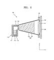
- FIG. 5A is a schematic view illustrating deposition of the deposition material 115 in the thin film deposition apparatus 100, according to an embodiment of the present invention.
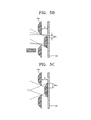
- FIG. 5B illustrates a shadow zone of a thin film deposited on the substrate 160 when the deposition space is partitioned by the barrier walls 131.
- FIG. 5C illustrates a shadow zone of a thin film deposited on the substrate 160 when the deposition space is not partitioned.
- the deposition material 115 that is vaporized in the deposition source 110 is deposited on the substrate 160 by being discharged through the first nozzle 120 and the second nozzle 150. Since the space between the first nozzle 120 and the second nozzle 150 is partitioned by the barrier walls 131, the deposition material 115 discharged through each of the first slits 121 of the first nozzle 120 is not mixed with the deposition material 115 discharged through the other adjacent first slits 121 due to the barrier walls 131.
- the deposition material 115 is deposited on the substrate 160 through the second nozzle 150 at an angle of about 55° to about 90°, as illustrated in FIG. 5B .
- the deposition material 115 passing through a second slit 151 away from the middle of each of the sub-deposition spaces is deposited at an angle of about 55°
- the deposition material 115 passing through a second slit 151 of the second nozzle 150 in the middle of each of the sub-deposition spaces is deposited at an angle of about 90°.
- the width SH 1 of the shadow zone formed on the substrate 160 is determined according to Equation 1.
- SH 1 s * d s / h
- the deposition material 115 is discharged through the second nozzle 150 in a wider range of angles than in the case of FIG. 5B .
- a width SH 2 of a shadow zone formed on the substrate 160 is much greater than when the deposition space is partitioned by the barrier walls 131.
- the width SH 2 of the shadow zone formed on the substrate 160 is determined according to Equation 2.
- SH 2 s * 2 ⁇ d / h
- d s which is the width of the first slits 121, is a few to tens times smaller than d, which is the interval between the adjacent barrier walls 131, and thus the shadow zone may have a smaller width when the space between the first nozzle 120 and the second nozzle 150 is partitioned by the barrier walls 131.
- the width SH 2 of the shadow zone formed on the substrate 160 may be reduced by either one of the followings: (1) by reducing the interval ("d") between the adjacent barrier walls 131, (2) by reducing the distance ("s") between the second nozzle 150 and the substrate 160, or (3) by increasing the distance ("h") between the the first nozzle 120 and the second nozzle 150.
- the shadow zone formed on the substrate 160 may be reduced by installing the barrier walls 131.
- the second nozzle 150 can be separated from the substrate 160.
- the second nozzle 150 may be separated from the substrate 160 by a predetermined distance.
- deposition is performed with the FMM in close contact with a substrate in order to prevent formation of a shadow zone on the substrate.
- the contact may cause defects.
- the second nozzle 150 is disposed to be separated from the substrate 160 by a predetermined distance. This may be facilitated by installing the barrier walls 131 to reduce the width of the shadow zone formed on the substrate 160.
- a defect caused due to the contact between a substrate and a FMM, which occurs in a conventional deposition method may be prevented.
- the manufacturing time since it is unnecessary to dispose the FMM in close contact with the substrate during a deposition process, the manufacturing time may be reduced.
- interval control member and an alignment control member which can be used to obtain sufficient alignment precision and interval precision between the second nozzle 150 and the substrate 160 in the thin film deposition apparatus 100 according to some embodiments of the present invention will be described in detail.
- the interval control member and an alignment control member form part of an adjustment member in this embodiment.
- the adjustment member comprises both the interval control member and the alignment control member.
- the adjustment member can comprise one of the interval control member or the alignment control member.
- the second nozzle 150 is separated from the substrate 160 by a predetermined distance, and deposition is performed while the second nozzle 150 is moved relative to the substrate 160 in the Z-axis direction.
- positional precision between the second nozzle 150 and the substrate 160 is very significant.
- pattern position may be shifted when the interval between the second nozzle 150 and the substrate 160 varies.
- the interval between the second nozzle 150 and the substrate 160 has to be maintained as constant as possible, for example, at 100um.
- the thin film deposition apparatus 100 according to the current embodiment of the present invention includes an interval control member and an alignment control member.
- the interval between the second nozzle 150 and the substrate 160 may be maintained constant, and at the same time the second nozzle 150 and the substrate 160 may be precisely aligned with each other.
- FIG. 6 is a schematic side cross-sectional view of the thin film deposition apparatus 100 of FIG. 1 , according to an embodiment of the present invention.
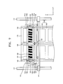
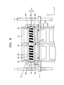
- FIG. 7 is a schematic front view of the thin film deposition apparatus 100, illustrating an interval control member and an alignment control member according to an embodiment of the present invention.
- all the elements of the thin film deposition apparatus 100 of FIG. 6 excluding the second nozzle 150, the second nozzle frame 155 and the substrate 160, are not illustrated in FIG. 7 .
- the thin film deposition apparatus 100 includes a base frame 171, a tray 173, an open mask 175, rails 177, the interval control member, and the alignment control member.
- the substrate 160 includes a deposition region 161 in which a deposition material is deposited, and a non-deposition region 162 in which no deposition material is deposited.
- the substrate 160 includes positioning marks 163, which are used as reference marks to maintain the interval between the second nozzle 150 and the substrate 160 to be constant and to precisely align the second nozzle 150 and the substrate 160 with respect to each other. Although three positioning marks 163 that are respectively formed in a left edge region, a center region, and a right edge region of the substrate 160 are illustrated in FIG. 7 , embodiments of the present invention are not limited thereto.
- the open mask 175 is arranged on the substrate 160. If the substrate 160 is large enough to manufacture, the substrate 160 may include a plurality of deposition regions 161, and non-deposition regions 162 on which no deposition material is to be deposited and which are respectively positioned between adjacent deposition regions 161. In order to prevent deposition of the deposition material in the non-deposition regions 162, the open mask 175 is used. However, it is difficult to precisely adjust the interval between the second nozzle 150 and the substrate and the positions thereof with a common open mask.
- the open mask 175 is arranged such as to expose a region of the substrate 160 that extends in the same direction, i.e., the Z-axis direction, as a direction in which the second nozzle 150 is moved.
- the open mask 175 is arranged not to overlap the regions of the substrate 160 where the positioning marks 163 are formed, thereby allowing to adjust the interval between the second nozzle 150 and the substrate 160 and the positions thereof.
- the rails 177 are disposed on opposite sides of the substrate 160, which is a deposition target on which the deposition material 115 is to be deposited.
- the base frame 171 is inserted between the rails 177.
- the base frame 171 is moved up and down in the Z-axis direction along the rails 177 due to a driving force of a motor (not shown).
- All the elements of the thin film deposition apparatus 100 that are involved in maintaining a constant interval between the second nozzle 150 and the substrate 160 and in precisely aligning the second nozzle 150 and the substrate 160 with respect to each other, i.e., the second nozzle 150, the second nozzle frame 155, the tray 173, the interval control member and the alignment control member are disposed on the base frame 171.
- the tray 173 is mounted on the base frame 171
- the second nozzle frame 155 is installed in the tray 173.
- the interval control member is disposed between the tray 173 and the second nozzle frame 155
- the alignment control member is disposed between the base frame 171 and the tray 173.
- the weight of the base frame 171 may be as light as possible.
- motors (not shown), which are disposed on opposite sides of the base frame 171 to move the base frame 171 in the Z-axis direction, may provide a driving force sufficient to drive all the elements disposed on the base frame 171.
- the motors have to be operable in a vacuum and have to have the same moving speed and sufficiently low vibration.
- the moving speed of the motors in the Z-axis direction may not be precisely controlled. However, in order to minimize vibration when the motors are operating, the motors have to be moved at a speed as constant as possible.
- the tray 173 is disposed on the base frame 171.
- the second nozzle frame 155 is installed to be detachable from the tray 173.
- the second nozzle frame 155 when the second nozzle frame 155 is installed in the tray 173, the second nozzle frame 155 is restricted from moving in the Y-axis and Z-axis directions. However, the second nozzle frame 155 is movable to some extent in the X-axis direction within the tray 173 when the second nozzle frame 155 is installed in the tray 173. In other words, the interval between the substrate 160 and the second nozzle 150 may be adjusted by moving the second nozzle frame 155 relative to the tray 173 in the X-axis direction.
- the tray 173 may be moved relative to the base frame 171 in the Y-axis and Z-axis directions by a first alignment adjusting actuator 191 and a second alignment adjusting actuator 192, which will be described later.
- the tray 173 is fixed not to move in the X-axis direction.
- the second nozzle 150 and the substrate 160 may be precisely aligned with each other in the Y-axis and Z-axis directions by moving the tray 173 relative to the base frame 171 along a YZ plane.
- the interval control member includes a first interval adjusting actuator 181, a second interval adjusting actuator 182, a third interval adjusting actuator 183, and first through fourth interval adjusting sensors 185a, 185b, 185c and 185d.
- the first interval adjusting actuator 181, the second interval adjusting actuator 182, and the third interval adjusting actuator 183 may be installed between the tray 173 and the second nozzle frame 155.
- the first through fourth interval adjusting sensors 185a, 185b, 185c and 185d may be mounted on the second nozzle frame 155.
- an actuator generically refers to a driving apparatus using electricity, hydraulic pressure, compressed air, or the like, and in particular, refers to, in the mechatronics field, an electrical motor with a kind of control tool, or a piston or cylinder machine operated by hydraulic pressure or air pressure.
- the first interval adjusting actuator 181 is disposed between a side of the tray 173, i.e., a left side of the tray 173 in FIG. 7 , and the second nozzle frame 155, to adjust the interval between the second nozzle frame 155 or the second nozzle 150 enclosed by the second nozzle frame 155, and the substrate 160.
- the second interval adjusting actuator 182 is disposed between a side of the tray 173, i.e., a right side of the tray 173 in FIG. 7 , and the second nozzle frame 155, to adjust the interval between the second nozzle frame 155 or the second nozzle 150 enclosed by the second nozzle frame 155, and the substrate 160.
- the third interval adjusting actuator 183 is disposed on a base of the tray 173, i.e., at a bottom center of the tray 173 in FIG. 7 , to adjust the interval between the second nozzle frame 155 or the second nozzle 150 enclosed by the second nozzle frame 155, and the substrate 160.
- piezoelectric motors may be used as the first interval adjusting actuator 181, the second interval adjusting actuator 182, and the third interval adjusting actuator 183.
- a piezoelectric motor which is a kind of an electrical motor generating a driving force from a piezoelectric material that deforms as an electrical field is applied, is widely used as a small-sized actuator producing a strong driving force.
- first through fourth interval adjusting sensors 185a, 185b, 185c and 185d may be mounted on the four corners of the second nozzle frame 155, respectively.
- the first through fourth interval adjusting sensors 185a, 185b, 185c and 185d measure the interval between the second nozzle frame 155 and the substrate 160.
- the first through fourth interval adjusting sensors 185a, 185b, 185c and 185d may measure the interval between the second nozzle frame 155 and the substrate 160 by using laser.
- the first through fourth interval adjusting sensors 185a, 185b, 185c and 185d may measure the interval between the second nozzle frame 155 and the substrate 160 by using the positioning marks 163 on the substrate 160.
- a method of adjusting the interval between the second nozzle 150 and the substrate 160 by using the interval control member described above will be described later in detail with reference to FIG. 8 .
- the alignment control member includes the first alignment adjusting actuator 191, the second alignment adjusting actuator 192, and first through fourth alignment adjusting sensors 195a, 195b, 195c and 195d.
- the first alignment adjusting actuator 191 and the second alignment adjusting actuator 192 may be installed between the base frame 171 and the tray 173.
- the first through fourth alignment adjusting sensors 195a, 195b, 195c and 195d may be mounted on the second nozzle frame 155.
- the first alignment adjusting actuator 191 is disposed between a side of the base frame 171, i.e., a left side of the base frame 171 in FIG. 7 , and the left side of the tray 173, to adjust alignment among the tray 173, the second nozzle 150 installed in the tray 173, and the substrate 160 in the Y-axis direction.
- the second alignment adjusting actuator 192 is disposed between a base of the base frame 171 and a bottom of the tray 173, and in particular, between a right base region of the base frame 171 and a right bottom edge of the tray 173 in FIG. 7 , to control rotation angles of the tray 173 and the second nozzle 150, which is installed in the tray 173, with respect to the substrate 160, and thus to adjust alignment between the second nozzle 150 and the substrate 160.
- first through fourth alignment adjusting sensors 195a, 195b, 195c and 195d may be mounted on the four corners of the second nozzle frame 155, respectively.
- the first through fourth alignment adjusting sensors 195a, 195b, 195c and 195d measure whether the second nozzle frame 155 and the substrate 160 are aligned with each other.
- the first through fourth alignment adjusting sensors 195a, 195b, 195c and 195d may measure whether the second nozzle frame 155 and the substrate 160 are aligned with each other, by using laser.
- the first through fourth adjustment adjusting sensors 195a, 195b, 195c and 195d may measure whether the second nozzle frame 155 and the substrate 160 are aligned with each other, by using the positioning marks 163 on the substrate 160.
- a method of aligning the second nozzle 150 and the substrate 160 with each other by using the alignment control member will be described later in detail with reference to FIGS. 9A and 9B .
- FIG. 8 is a front view for describing a method of adjusting the interval between the second nozzle 150 and the substrate 160 to be constant by using the interval control member, according to an embodiment of the present invention.
- basically three actuators are used in this embodiment in order to adjust the interval between the second nozzle 150 and the substrate 160, as described above.
- Other embodiments may use a different number of actuators or sensors for the interval control member.
- the second nozzle frame 155 is moved relative to the tray 173 in the X-axis direction by a predetermined distance by driving the first interval adjusting actuator 181, such that an average of the intervals between the second nozzle 150 and the substrate 160 measured by the first interval adjusting sensor 185a and the third interval adjusting sensor 185c reaches a desired value, for example,100 ⁇ m.
- the first interval adjusting actuator 181 moves the second nozzle frame 155 relative to the tray 173 such that a region of the second nozzle frame 155 in which the first interval adjusting actuator 181 is disposed is shifted closer to the substrate 160.
- the first interval adjusting actuator 181 moves the second nozzle frame 155 relative to the tray 173 such that the region of the second nozzle frame 155 in which the first interval adjusting actuator 181 is disposed is shifted away from the substrate 160.
- the second nozzle frame 155 is moved relative to the tray 173 in the X-axis direction by a predetermined distance by driving the second interval adjusting actuator 182, such that an average of the intervals between the second nozzle 150 and the substrate 160 measured by the second interval adjusting sensor 185b and the fourth interval adjusting sensor 185d reaches a desired value, for example, 1 00 ⁇ m.
- the second interval adjusting actuator 182 moves the second nozzle frame 155 relative to the tray 173 such that a region of the second nozzle frame 155 in which the second interval adjusting actuator 182 is disposed is shifted closer to the substrate 160.
- the second interval adjusting actuator 182 moves the second nozzle frame 155 relative to the tray 173 such that the region of the second nozzle frame 155 in which the second interval adjusting actuator 182 is disposed is shifted away from the substrate 160.
- the intervals between the second nozzle 150 and the substrate 160 on the left and right sides are adjusted by controlling the average of the intervals measured by the first interval adjusting sensor 185a and the third interval adjusting sensor 185c and the average of the intervals measured by the second interval adjusting sensor 185b and the fourth interval adjusting sensor 185d.
- the second nozzle frame 155 is rotated relative to the tray 173 around an axis A in FIG. 8 by driving the third interval adjusting actuator 183. In other words, the second nozzle frame 155 can be rotated about axis A.
- the second nozzle frame 155 is moved by driving the third interval adjusting actuator 183 such that a region of the second nozzle frame 155 in which the third interval adjusting actuator 183 is disposed is shifted closer to the substrate 160.
- the second nozzle frame 155 is moved by driving the third interval adjusting actuator 183 such that the region of the second nozzle frame 155 in which the third interval adjusting actuator 183 is disposed is shifted away from the substrate 160.
- the position of the pattern is maintained consistent, and the reliability of products is improved.
- the interval between the second nozzle 150 and the substrate 160 may be precisely adjusted by using greater numbers of interval adjusting actuators and interval adjusting sensors.
- FIGS. 9A and 9B are front views for describing a method of adjusting alignment between the second nozzle 150 and the substrate 160 in the thin film deposition apparatus 100 by using the alignment control member, according to an embodiment of the present invention.
- basically two actuators are used in this embodiment in order to align the second nozzle 150 and the substrate 160 with each other, as described above.
- the second nozzle 150 in FIG. 7 and the open mask 175 in FIG. 7 are not illustrated in FIGS. 9A and 9B .
- Other embodiments may use a different number of actuators or sensors for the alignment control member.
- Y-axis directional relative positions of the positioning marks 163 in the substrate 160 and alignment marks (not shown) in the second nozzle frame 155 are measured by using the first alignment adjusting sensor 195a, the second alignment adjusting sensor 195b, the third alignment adjusting sensor 195c and the fourth alignment adjusting sensor 195d. If the substrate 160 and the second nozzle frame 155 are not aligned with each other (i.e. not in the correct position in plane parallel to a surface of the substrate), the tray 173 is moved by a predetermined distance in the Y-axis direction by driving the first alignment adjusting actuator 191, to align the substrate 160 and the second nozzle frame 155 with each other in the Y-axis direction.
- the amount of movement of the tray 173 in the Y-axis direction may be set to be an average difference between the distances from the positioning marks 163 in the substrate 160 to the alignment marks in the second nozzle frame 155 measured by the first through fourth alignment sensors 195a, 195b, 195c, and 195d.
- the second nozzle frame 155 is biased to the right side of the substrate 160 (see dashed lines in FIG. 9A ), the second nozzle frame 155 is moved relative to the substrate 160 by a predetermined distance in a direction of an arrow B by driving the first alignment adjusting actuator 191, to align the substrate 160 and the second nozzle frame 155 with each other in the Y-axis direction.
- the second nozzle 150 and the substrate 160 may not be aligned with each other when the second nozzle 150 is rotated relative to the substrate 160 by a predetermined angle.
- the second nozzle 150 may be rotated in an opposite direction by the predetermined angle in order to align the second nozzle 150 and the substrate 160 with each other.
- the tray 173 is rotated by a predetermined angle by driving the second alignment adjusting actuator 192 such that the difference between the distances from the positioning marks 163 in the substrate 160 to the alignment marks in the second nozzle frame 155 measured by the first alignment adjusting sensor 195a and the third alignment adjusting sensor 195c and the difference between the distances from the positioning marks 163 in the substrates 160 to the alignment marks in the second nozzle frame 155 measured by the second alignment adjusting sensor 195b and the fourth alignment adjusting sensor 195d are to be zero.
- the substrate 160 and the second nozzle frame 155 are aligned with each other.
- the second alignment adjusting actuator 192 rotates the second nozzle frame 155 clockwise, i.e. in a direction of an arrow C, relative to the substrate 160.
- the second alignment adjusting actuator 192 rotates the second nozzle frame 155 counterclockwise.
- a precise thin film pattern may be formed on the substrate 160 while the second nozzle 150 is moved.
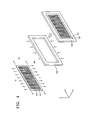
- FIG. 10 is a schematic perspective view of a thin film deposition apparatus 100 according to another embodiment of the present invention.
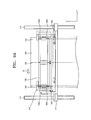
- FIG. 11 is a front view of the thin film deposition apparatus 100 of FIG. 10 , illustrating an interval control member 280 and an alignment control member (not shown) according to an embodiment of the present invention.
- all the elements of the thin film deposition apparatus 100 of FIG. 10 excluding the second nozzle 150, the second nozzle frame 155 and the substrate 160, are not illustrated in FIG. 11 .
- the thin film deposition apparatus 100 includes a deposition source 110, a first nozzle 120, a barrier wall assembly 130, the second nozzle 150, the second nozzle frame 155, the substrate 160, the alignment control member (not shown) and the interval control member 280.
- FIG. 12A illustrates a roller 280a constituting the interval control member 280, according to an embodiment of the present invention.
- the roller 280 constituting the interval control member 280
- the roller 280 may be attached to each of the four corners of the second nozzle frame 155.
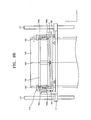
- FIG. 12B illustrates a ball 280b constituting the interval control member 280, according to another embodiment of the present invention.
- the ball 280b constituting the interval control member 280, may be attached to each of the four corners of the second nozzle frame 155.
- Diameters of the rollers 280a or the balls 280b, which constitute the interval control member 280, and diameters of axes thereof (not shown) may be precisely processed. If the interval control member 280 is constituted by the balls 280b, regions of the second nozzle frame 155 that contact the balls 280b may be precisely processed.
- the interval control member 280 according to the current embodiment of the present invention which is constituted by the rollers 280a or the balls 280b, may be manufactured to have a slightly lower degree of precision compared to the interval control member according to the previous embodiment described with reference to FIG. 6 .
- the interval control member 280 has a simple structure, may be easily manufactured, and does not interfere with the open mask 175.
- the interval control member 280 according to the current embodiment has a structure pressing the substrate 160, and thus the open mask 175 may be disposed under the interval control member 280.
- the open mask 175 may be installed relatively easily.
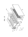
- FIG. 13 is a schematic perspective view of a thin film deposition apparatus 300 according to another embodiment of the present invention.
- the thin film deposition apparatus 300 includes a deposition source 310, a first nozzle 320, a first barrier wall assembly 330, a second barrier wall assembly 340, a second nozzle 350, a second nozzle frame 355, and a substrate 360.
- the first nozzle 320 is downstream of the deposition source 310, and the second nozzle 350 is downstream of the first nozzle 320.
- the first barrier wall assembly 330 and the second barrier wall assembly 340 are located between the first nozzle 320 and the second nozzle 350.
- the first nozzle 320 can be considered to be a first nozzle member including a plurality of openings (e.g. slits).
- the second nozzle 350 can be considered to be a second nozzle member including a second plurality of openings (e.g. slits).
- the thin film deposition apparatus 300 may include additional and/or different components, such as in the examples described below. In particular, the embodiment shown in FIGS.
- FIG. 13 can be combined with any of the features described with reference to FIGS. 1 to 12 .
- any of features associated with the arrangements in FIGS. 1 to 12 that include one barrier wall assembly 330 could be used with a first barrier wall assembly 330 and a second barrier wall assembly 340 as shown in FIG. 13 .
- all the components of the thin film deposition assembly 300 may be disposed within a chamber that is maintained at an appropriate degree of vacuum.
- the chamber is maintained at an appropriate vacuum in order to allow a deposition material to move in a substantially straight line through the thin film deposition apparatus 300.
- the substrate 360 which constitutes a deposition target on which a deposition material 315 is to be deposited, is disposed in the chamber.
- the deposition source 310 that contains and heats the deposition material 315 is disposed in an opposite side of the chamber to a side in which the substrate 360 is disposed.
- the deposition source 310 may include a crucible 311 and a heater 312.
- the first nozzle 320 is disposed at a side of the deposition source 310 facing the substrate 360.
- the first nozzle 320 includes a plurality of first slits 321 arranged at equal intervals in a Y-axis direction.
- the first barrier wall assembly 330 is disposed at a side of the first nozzle 320.
- the first barrier wall assembly 330 includes a plurality of first barrier walls 331, and a first barrier wall frame 332 that covers sides of the first barrier walls 331.
- the second barrier wall assembly 340 is disposed at a side of the first barrier wall assembly 330.
- the second barrier wall assembly 340 includes a plurality of second barrier walls 341, and a second barrier wall frame 342 that covers sides of the second barrier walls 341.
- the second nozzle 350 and the second nozzle frame 355 are disposed between the deposition source 310 and the substrate 360.
- the second nozzle frame 355 may be formed in a lattice shape, similar to a window frame.
- the second nozzle 350 is bound inside the second nozzle frame 355.
- the second nozzle 350 includes a plurality of second slits 351 arranged at equal intervals in the Y-axis direction.
- the thin film deposition assembly 300 includes two separate barrier wall assemblies, i.e., the first barrier wall assembly 330 and the second barrier wall assembly 340.
- the plurality of first barrier walls 331 may be arranged parallel to each other at equal intervals in the Y-axis direction.
- each of the first barrier walls 331 may be formed to extend along an XZ plane in FIG. 13 , i.e., perpendicular to the Y-axis direction.
- the plurality of second barrier walls 341 may be arranged parallel to each other at equal intervals in the Y-axis direction.
- each of the second barrier walls 341 may be formed to extend along the XZ plane in FIG. 13 , i.e., perpendicular to the Y-axis direction.
- the deposition space is divided by the first barrier walls 331 and the second barrier walls 341 into sub-deposition spaces that respectively correspond to the first slits 321 through which the deposition material 315 is discharged.
- the second barrier walls 341 may be disposed to correspond to the first barrier walls 331.
- the second barrier walls 341 may be respectively aligned with the first barrier walls 331 to be parallel thereto on the same plane as the first barrier walls 331.
- Each pair of the corresponding first and second barrier walls 331 and 341 may be located on the same plane.
- the deposition material 315 discharged through each of the first slits 321 is not mixed with the deposition material 315 discharged through the other first slits 321, and is deposited on the substrate 360 through the second slits 351.
- the first barrier walls 331 and the second barrier walls 341 guide the deposition material 315, which is discharged through the first slits 321, so as not to flow in the Y-axis direction.
- first barrier walls 331 and the second barrier walls 341 are respectively illustrated as having the same thickness in the Y-axis direction, aspects of the present invention are not limited thereto.
- the second barrier walls 341, which should be accurately aligned with the second nozzle 350 may be formed to be relatively thin, whereas the first barrier walls 331, which do not need to be precisely aligned with the second nozzle 350, may be formed to be relatively thick. This makes it easier to manufacture the thin film deposition apparatus 300.
- the thin film deposition apparatus 300 may further include an interval control member and an alignment control member in some embodiments of the invention.
- the interval control member according to the current embodiment of the present invention may be constituted by actuators and sensors as in the embodiments described with reference to FIGS. 7 to 9 , or alternatively, by rollers or balls as in the embodiments described with reference to FIGS. 12A and 12B .
- the alignment control member according to the current embodiment of the present invention may be constituted by actuators and sensors as in the embodiments described with reference to FIGS. 7 to 9 and to FIGS. 10 and 11 . Since the interval control member and the alignment control member have been described in detail in the previous embodiments, a detailed description thereof will not be provided here.
- the current embodiment differs from the previous embodiment described with reference to FIG. 1 in that no barrier wall assembly is disposed.
- FIG. 14 is a schematic perspective view of a thin film deposition apparatus 900 according to an embodiment of the present invention
- FIG. 15 is a schematic side view of the thin film deposition apparatus 900
- FIG. 16 is a schematic plan view of the thin film deposition apparatus 900.
- the thin film deposition apparatus 900 includes a deposition source 910, a first nozzle 920, and a second nozzle 950.
- the first nozzle 920 is downstream of the deposition source 910, and the second nozzle 950 is downstream of the first nozzle 920.
- the first nozzle 920 can be considered to be a first nozzle member including a plurality of openings (e.g. slits).
- the second nozzle 950 can be considered to be a second nozzle member including a second plurality of openings (e.g. slits).
- the thin film deposition apparatus 910 may include additional and/or different components, such as in the examples described below.
- all the components of the thin film deposition assembly 900 may be disposed within a chamber that is maintained at an appropriate degree of vacuum.
- the chamber is maintained at an appropriate vacuum in order to allow a deposition material to move in a substantially straight line through the thin film deposition apparatus 900.
- the chamber In order to deposit the deposition material 915 that is emitted from the deposition source 910 and discharged through the first nozzle 920 and the second nozzle 950 on a substrate in a desired pattern, the chamber should be maintained in a high-vacuum state as in a deposition method using a fine metal mask (FMM).
- the temperature of the second nozzle 950 has to be sufficiently lower than the temperature of the deposition source 910. In this regard, the temperature of the second nozzle 950 may be about 100°C or less. The temperature of the second nozzle 950 should be sufficiently low so as to reduce thermal expansion of the second nozzle 950.
- the substrate 400 which constitutes a deposition target on which the deposition material 915 is to be deposited, is disposed in the chamber.
- the substrate 400 may be a substrate for flat panel displays.
- a large substrate, such as a mother glass, for manufacturing a plurality of flat panel displays, may be used as the substrate 400.
- Other substrates may also be employed.
- deposition may be performed while the substrate 400 or the thin film deposition apparatus 900 is moved relative to each other.
- the size of the FMM has to be equal to the size of a substrate.
- the size of the FMM has to be increased as the substrate becomes larger.
- deposition may be performed while the thin film deposition apparatus 900 or the substrate 400 is moved relative to each other.
- deposition may be continuously performed while the substrate 400, which is disposed such as to face the thin film deposition apparatus 900, is moved in the Z-axis direction.
- deposition is performed in a scanning manner while the substrate 400 is moved in a direction of arrow A in FIG. 14 .
- the substrate 400 is illustrated as being moved in the Z-axis direction in FIG. 14 when deposition is performed, embodiments of present invention are not limited thereto.
- Deposition may be performed while the thin film deposition apparatus 900 is moved in the Y-axis direction, whereas the substrate 400 is fixed.
- the second nozzle 950 may be significantly smaller than a FMM used in a conventional deposition method.
- deposition is continuously performed, i.e., in a scanning manner while the substrate 400 is moved in the Z-axis direction.
- lengths of the second nozzle 950 in the Z-axis and Y-axis directions may be significantly less than the lengths of the substrate 400 in the XZ-axis and Y-axis directions.
- the second nozzle 950 since the second nozzle 950 may be significantly smaller than a FMM used in a conventional deposition method, it is relatively easy to manufacture the second nozzle 950.
- the use of the second nozzle 950 which is smaller than a FMM used in a conventional deposition method, is more convenient in all processes, including etching and subsequent other processes, such as precise extension, welding, moving, and cleaning processes, compared to the conventional deposition method using the larger FMM. This is advantageous for a relatively large display device.
- the thin film deposition assembly 900 and the substrate 400 may be separated from each other by a predetermined distance. This will be described later in detail.
- the deposition source 910 that contains and heats the deposition material 915 is disposed in an opposite side of the chamber to a side in which the substrate 400 is disposed. As being vaporized in the deposition source 910, the deposition material 915 is deposited on the substrate 400.
- the deposition source 910 includes a crucible 911 and a heater 915.
- the crucible 911 holds the deposition material 915.
- the heater 911 heats the crucible 911 to vaporize the deposition material 915 contained in the crucible 912 towards a side of the crucible 911, and in particular, towards the first nozzle 920.
- the first nozzle 920 is disposed at a side of the deposition source 910 facing the substrate 400.
- the first nozzle 920 includes a plurality of first slits 921 arranged at equal intervals in the Z-axis direction in which the substrate 400 is scanned.
- the deposition material 915 vaporized in the deposition source 910 passes through the first nozzle 920 towards the substrate 400.
- the first nozzle 920 includes the plurality of first slits 921 arranged in the Z-axis direction, that is, the scanning direction of the substrate 400
- a size of a pattern formed from the deposition material 910 discharged through the second slits 9510 of the second nozzle 950 is exclusively affected by the size of one first slit 921 (since this may be considered as if only one first slit 921 is disposed in the Y-axis direction), and thus no shadow zone appears on the substrate 400.
- the plurality of first slits 921 are arranged in the scanning direction of the substrate 400, even if there is a difference between fluxes of the first slits 921 of the first nozzle 920, the difference may be compensated for, thereby constantly maintaining deposition uniformity.
- the second nozzle 950 and the second nozzle frame 955 are disposed between the deposition source 910 and the substrate 400.
- the second nozzle frame 955 may be formed in a lattice shape, similar to a window frame.
- the second nozzle 950 is bound inside the second nozzle frame 155.
- the second nozzle 950 includes a plurality of second slits 951 arranged at equal intervals in the Y-axis direction.
- the deposition material 915 vaporized in the deposition source 910 passes through the first nozzle 920 and the second nozzle 950 towards the substrate 400.
- the second nozzle 950 may be manufactured by etching, which is the same method as used in a conventional method of manufacturing an FMM, and in particular, a striped FMM.
- the total number of first slits 921 may be greater than the total number of second slits 951.
- the deposition source 910 and the first nozzle 920 coupled to the deposition source 910 may be separated from the first nozzle 950 by a predetermined distance.
- the deposition source 910 and the first nozzle 950 coupled to the first nozzle 920 may be connected to the second nozzle 950 by a connection member 935, as illustrated in FIG. 14 . That is, the deposition source 910, the first nozzle 920 and the second nozzle 950 may be integrally formed as one body by being connected to each other via the connection member 935.
- the connection member 935 guides the deposition material 915, which is discharged through the first slits 921, to move straight, and limits the flow in the Y-axis direction.
- connection members 935 are illustrated as being disposed on left and right sides of the deposition source 910, the first nozzle 920 and the second nozzle 950 to guide the deposition material 915 to limit the flow in the Y-axis direction and Z-axis direction, the present invention is not limited thereto.
- the connection member 935 may be formed as a sealed box to guide flow of the deposition material 915 both in the Z-axis and Y-axis directions.
- the thin film deposition apparatus 900 performs deposition while being moved relative to the substrate 400.
- the second nozzle 950 may be separated from the substrate 400 by a predetermined distance.
- the FMM in close contact with a substrate in order to prevent formation of a shadow zone on the substrate.
- the contact may cause defects.
- the size of the mask has to be the same as the size of the substrate since the mask cannot be moved relative to the substrate.
- the size of the mask has to be increased as display devices become larger.
- the second nozzle 950 is disposed to be separated from the substrate 400 by a predetermined distance.
- a mask is formed to be smaller than a substrate, and deposition is performed while the mask is moved relative to the substrate.
- the mask can be easily manufactured.
- defects caused due to the contact between a substrate and a FMM, which occur in the conventional deposition method, may be prevented.
- the manufacturing time may be reduced.
- the thin film deposition apparatus 900 may include an interval control member and an alignment control member.
- the interval between the second nozzle 950 and the substrate 400 may be maintained constant, and at the same time the second nozzle 950 and the substrate 400 may be precisely aligned with each other. Controlling the interval and alignment between the second nozzle 950 and the substrate 400 are described in the previous embodiment with reference to FIGS. 7 to 9 , and thus a detailed description thereof will not be provided here.
- interval control member and an alignment control member form part of an adjustment member in this embodiment.
- the adjustment member comprises both the interval control member and the alignment control member.
- the adjustment member can comprise one of the interval control member or the alignment control member.
- no adjustment member or interval control member or alignment control member may be present.
- a first nozzle 920 includes a plurality of first slits 921 that are arranged to tilt by a predetermined angle, unlike the previous embodiment described with reference to FIGS. 14 to 16 .
- FIG. 17 is a schematic perspective view of a thin film deposition apparatus 900 according to another embodiment of the present invention.
- the thin film deposition apparatus 900 includes a deposition source 910, the first nozzle 920, and a second nozzle 950.
- the deposition source 910 includes a crucible 911 that is filled with the deposition material 915, and a heater 911 that heats the crucible 911 to vaporize the deposition material 915, which is contained in the crucible 912, towards a side of the crucible 911, and in particular, towards the first nozzle 920.
- the first nozzle 920 is disposed at a side of the deposition source 910.
- the first nozzle 920 includes a plurality of first nozzles 921 arranged in the Z-axis direction.
- the second nozzle 950 and a second nozzle frame 955 are further disposed between the deposition source 910 and the substrate 400.
- the second nozzle 950 includes a plurality of second slits 951 arranged in the Y-axis direction.
- the deposition source 910 and the first nozzle 920 coupled to the deposition source 920, and the second nozzle 950, which is spaced away from the first nozzle 920, are connected by the connection member 935.
- the plurality of first slits 921 of the first nozzle 920 are tilted at a predetermined angle, unlike the previous embodiment described with reference to FIGS. 14 to 16 .
- the first slits 921 may include first slits 921 a and 921 b arranged in respective rows.
- the first slits 921 a and 921 b may be arranged in respective rows to alternate in a zigzag pattern.
- the first slits 921 a and 921 b may be tilted by a predetermined angle with respect to an XZ plane.
- the first slits 921 a and 921 b may be arranged to tilt by a predetermined angle.
- the first slits 921 a in a first row and the first slits 921 b in a second row may tilt towards each other. That is, the first slits 921 a of the first row in a left part of the first nozzle 920 may tilt to face a right end portion of the second nozzle 950, and the first slits 921 b of the second row in a right part of the first nozzle 920 may tilt to face a left end portion of the second nozzle 950.
- FIG. 18 is a graph showing a thickness distribution of a deposition film that is formed on a substrate while the first slits 921 a and 921 b in the first nozzle 920, which is adjacent to the deposition source 910, are not tilted in the thin film deposition apparatus according to the current embodiment of the present invention.
- FIG. 19 is a graph showing a thickness distribution of a deposition film that is formed on a substrate while the first slits 920a and 920b are tilted as in the thin film deposition apparatus according to the current embodiment of the present invention. Comparing FIGS. 18 and 19 , the thicknesses of the deposition film in opposite end portions of the substrate are relatively greater when the first slits 921 a and 921 b are tilted than when not tilted, thereby increasing uniformity of the deposition film.
- the deposition of the deposition material 915 may be adjusted to lessen a thickness variation between the center and the end portions of the substrate 400 and improve thickness uniformity of the deposition film. Moreover, utilization efficiency of the deposition material 915 may also be improved.
- the thin film deposition apparatus 900 may include an adjustment member including an interval control member and/or an alignment control member.
- an adjustment member including an interval control member and/or an alignment control member.
- the interval between the second nozzle 950 and the substrate 400 may be maintained constant, and at the same time the second nozzle 950 and the substrate 400 may be precisely aligned with each other. Controlling the interval and alignment between the second nozzle 950 and the substrate 400 are described in the previous embodiment with reference to FIGS. 7 to 9 , and thus a detailed description thereof will not be provided here.
- a thin film deposition apparatus constructed as described above may be easily manufactured and may be simply applied to manufacture large-sized display devices on a mass scale.
- the thin film deposition apparatus may improve manufacturing yield and deposition efficiency and may have a structure that allows the interval between a nozzle and a substrate to be easily adjusted.
Landscapes
- Chemical & Material Sciences (AREA)
- Chemical Kinetics & Catalysis (AREA)
- Engineering & Computer Science (AREA)
- Materials Engineering (AREA)
- Mechanical Engineering (AREA)
- Metallurgy (AREA)
- Organic Chemistry (AREA)
- Physical Vapour Deposition (AREA)
- Electroluminescent Light Sources (AREA)
Abstract
Description
- The present invention relates to a thin film deposition apparatus, and more particularly to a thin film deposition apparatus that can be simply applied to produce large-sized display devices on a mass scale and that improves manufacturing yield.
- Organic light-emitting display devices have a larger viewing angle, better contrast characteristics, and a faster response rate than some other types of display devices, and thus have drawn attention as a next-generation display device.
- Organic light-emitting display devices generally have a stacked structure including an anode, a cathode, and an emission layer interposed between the anode and the cathode. The devices display images in color when holes and electrons, injected respectively from the anode and the cathode, recombine in the emission layer and thus light is emitted. However, it is difficult to achieve high light-emission efficiency with such a structure, and thus intermediate layers, including an electron injection layer, an electron transport layer, a hole transport layer, a hole injection layer, or the like, are optionally additionally interposed between the emission layer and each of the electrodes.
- Also, it is practically very difficult to form fine patterns in organic thin films such as the emission layer and the intermediate layers, and red, green, and blue light-emission efficiency varies according to the organic thin films. For these reasons, it is not easy to form an organic thin film pattern on a large substrate, such as a mother glass having a size of 5G or more, by using a conventional thin film deposition apparatus, and thus it is difficult to manufacture large organic light-emitting display devices having satisfactory driving voltage, current density, brightness, color purity, light-emission efficiency, life-span characteristics. Thus, there is a demand for improvement in this regard.
- An organic light-emitting display device includes intermediate layers, including an emission layer disposed between a first electrode and a second electrode that are arranged opposite to each other. The electrodes and the intermediate layers may be formed via various methods, one of which is a deposition method. When an organic light-emitting display device is manufactured by using the deposition method, a fine metal mask (FMM) having the same pattern as a thin film to be formed is disposed to closely contact a substrate, and a thin film material is deposited over the FMM in order to form the thin film having the desired pattern.
- The present invention provides a thin film deposition apparatus that may be easily manufactured, that may be simply applied to manufacture large-sized display devices on a mass scale, that improves manufacturing yield and deposition efficiency, and that has a structure that allows an interval between a nozzle and a substrate to be easily adjusted.
- According to an aspect of the present invention, there is provided a thin film deposition apparatus as set out in claim 1. Prefered features of this aspect are set out in
claims 2 to 21. - In some embodiments, the deposition source, the first nozzle, the second nozzle, and the barrier wall assembly are movable relative to the substrate (for example, along a plane parallel to a surface of the substrate).
- In some embodiments, the deposition material is deposited on the substrate while the deposition source, the first nozzle, the second nozzle, and the barrier wall assembly are moved in relation to the substrate or the substrate is moved in relation to the deposition source, the first nozzle, the second nozzle, and the barrier wall assembly. In such embodiments, the relative movement of the thin film deposition apparatus and the substrate can be stepwise (i.e. deposit in one location and then move to the next location) or continuous (i.e. deposit while the relative movement occurs). In other embodiments, no relative movement is required.
- In some embodiments, the first openings comprise first slits and/or the second openings comprise second slits.According to an aspect of the present invention, there is provided a thin film deposition apparatus for forming a thin film on a substrate, the apparatus including: a deposition source; a first nozzle disposed at a side of the deposition source and including a plurality of first slits arranged in a first direction; a second nozzle disposed opposite to the first nozzle and including a plurality of second slits arranged in the first direction; a barrier wall assembly including a plurality of barrier walls that are arranged in the first direction in order to partition a space between the first nozzle and the second nozzle; and at least one of an interval control member that adjusts an interval between the second nozzle and the substrate, and an alignment control member that adjusts alignment between the second nozzle and the substrate.
- The interval control member may adjust the interval between the second nozzle and the substrate to be constant.
- The interval control member may include a sensor that senses a position of the second nozzle relative to the substrate, and an actuator that provides a driving force for moving the second nozzle relative to the substrate.
- The substrate may include a positioning mark, and the sensor may sense the position of the second nozzle relative to the substrate based on the positioning mark. In this regard, an open mask may be arranged on the substrate not to overlap with the positioning mask.
- The thin film deposition apparatus may further include: a base frame; and a tray that is arranged on the base frame and accommodates the second nozzle therein.
- The actuator may adjust the interval between the second nozzle and the substrate by moving the second nozzle relative to the tray.
- The interval control member may include: a first actuator that is disposed between a side of the second nozzle and the tray to move the second nozzle relative to the tray; a second actuator that is disposed between a side of the second nozzle opposite to the side of the second nozzle on which the first actuator is disposed and the tray to move the second nozzle relative to the tray; and a third actuator that rotates the second nozzle with respect to an axis parallel to the first direction.
- The actuator may include a piezoelectric motor.
- The actuator and the sensor may adjust the interval between the second nozzle and the substrate by real-time feedback control.
- The interval control member may include rollers or balls that are disposed at opposite end portions of the second nozzle and contact the substrate.
- The alignment control member may adjust a position of the second nozzle relative to the substrate to be constant.
- The alignment control member may include: a sensor that senses a position of the second nozzle relative to the substrate; and an actuator that provides a driving force for moving the second nozzle relative to the substrate.
- The substrate may include a positioning mark, and the sensor may sense the position of the second nozzle relative to the substrate based on the positioning mark. In this regard, an open mask may be arranged on the substrate not to overlap with the positioning mask.
- The thin film deposition apparatus may further include: a base frame; and a tray that is arranged on the base frame and accommodates the second nozzle therein.
- The actuator may adjust the alignment between the second nozzle and the substrate by moving the second nozzle relative to the tray.
- The alignment control member may include: a first actuator that is disposed between a side of the tray and the base frame to linearly move the tray relative to the base frame; and a second actuator that is disposed between a side of the tray opposite to the first actuator and the base frame to rotatably move the tray relative to the base frame.
- The actuator may include a piezoelectric motor.
- The actuator and the sensor may adjust the alignment between the second nozzle and the substrate by real-time feedback control.
- Each of the barrier walls may extend in a second direction that is substantially perpendicular to the first direction, in order to partition the space between the first nozzle and the second nozzle.
- The plurality of barrier walls may be arranged at equal intervals.
- The barrier walls may be separated from the second nozzle by a predetermined distance.
- The barrier wall assembly may be detachable from the thin film deposition apparatus.
- The barrier wall assembly may include a first barrier wall assembly including a plurality of first barrier walls, and a second barrier wall assembly including a plurality of second barrier walls.
- Each of the first barrier walls and each of the second barrier walls may extend in a second direction that is substantially perpendicular to the first direction, in order to partition the space between the first nozzle and the second nozzle.
- The first barrier walls may be arranged to correspond to the second barrier walls.
- Each pair of the corresponding first and second barrier walls may be arranged on substantially the same plane.
- A deposition material vaporized in the deposition source may be deposited on the substrate by being discharged through the first nozzle and the second nozzle.
- The second nozzle may be separated from the substrate by a predetermined distance.
- The deposition source, the first nozzle, the second nozzle, and the barrier wall assembly may be movable relative to the substrate, or the substrate may be movable relative to the deposition source, the first nozzle, the second nozzle, and the barrier wall assembly.
- The deposition material may be deposited on the substrate while the deposition source, the first nozzle, the second nozzle, and the barrier wall assembly are moved relative to the substrate or while the substrate is moved relative to the deposition source, the first nozzle, the second nozzle, and the barrier wall assembly.
- The deposition source, the first nozzle, the second nozzle, and the barrier wall assembly may be moved relative to the substrate along a plane parallel to a surface of the substrate, or the substrate may be moved relative to the deposition source, the first nozzle, the second nozzle, and the barrier wall assembly along the plane.
- According to an aspect of the present invention, there is provided a thin film deposition apparatus for forming a thin film on a substrate, the apparatus including: a deposition source that discharges a deposition material; a first nozzle disposed at a side of the deposition source and including a plurality of first slits arranged in a first direction; a second nozzle disposed opposite to the first nozzle and including a plurality of second slits arranged in a second direction perpendicular to the first direction; and at least one of an interval control member that adjusts an interval between the second nozzle and the substrate, and an alignment control member that adjusts alignment between the second nozzle and the substrate, wherein a deposition is performed while the substrate or the thin film deposition apparatus moves relative to each other in the first direction, and the deposition source, the first nozzle and the second nozzle are integrally formed as one body.
- The interval control member may adjust the interval between the second nozzle and the substrate to be constant.
- The interval control member may include: a sensor that senses a position of the second nozzle relative to the substrate; and an actuator that provides a driving force for moving the second nozzle relative to the substrate.
- The substrate may include a positioning mark, and the sensor may sense the position of the second nozzle relative to the substrate based on the positioning mark. In this regard, an open mask may be arranged on the substrate not to overlap with the positioning mask.
- The thin film deposition apparatus may further include: a base frame; and a tray that is arranged on the base frame and accommodates the second nozzle therein.
- The actuator may adjust the interval between the second nozzle and the substrate by moving the second nozzle relative to the tray.
- The interval control member may include: a first actuator that is disposed between a side of the second nozzle and the tray to move the second nozzle relative to the tray; a second actuator that is disposed between a side of the second nozzle opposite to the side of the second nozzle on which the first actuator is disposed and the tray to move the second nozzle relative to the tray; and a third actuator that rotates the second nozzle with respect to an axis parallel to the first direction.
- The actuator may include a piezoelectric motor.
- The actuator and the sensor may adjust the interval between the second nozzle and the substrate by real-time feedback control.
- The interval control member may include rollers or balls that are disposed at opposite end portions of the second nozzle and contact the substrate.
- The alignment control member may adjust a position of the second nozzle relative to the substrate to be constant.
- The alignment control member may include: a sensor that senses a position of the second nozzle relative to the substrate; and an actuator that provides a driving force for moving the second nozzle relative to the substrate.
- The substrate may further include a positioning mark, and the sensor senses the position of the second nozzle relative to the substrate based on the positioning mark. In this regard, an open mask may be arranged on the substrate not to overlap with the positioning mask.
- The thin film deposition apparatus may further include: a base frame; and a tray that is arranged on the base frame and accommodates the second nozzle therein.
- The actuator may adjust the alignment between the second nozzle and the substrate by moving the second nozzle relative to the tray.
- The alignment control member may include: a first actuator that is disposed between a side of the tray and the base frame to linearly move the tray relative to the base frame; and a second actuator that is disposed between a side of the tray opposite to the first actuator and the base frame to rotatably move the tray relative to the base frame.
- The actuator may include a piezoelectric motor.
- The actuator and the sensor may adjust the alignment between the second nozzle and the substrate by real-time feedback control.
- The deposition source, the first nozzle and the second nozzle may be integrally connected as one body by a connection member.
- The connection member may guide flow of the deposition material.
- The connection member may seal a space between the deposition source and the first nozzle, and the second nozzle.
- The thin film deposition apparatus may be separated from the substrate by a predetermined distance.
- The deposition material discharged from the thin film deposition apparatus may be continuously deposited on the substrate while the substrate or the thin film deposition apparatus may be moved relative to each other in the first direction.
- The second nozzle may be smaller than the substrate.
- The plurality of first slits may be tilted by a predetermined angle.
- The plurality of first slits may include first slits that are arranged in two rows along the first direction to tilt towards each other.
- The plurality of first slits may include first slits that are arranged in two rows along the first direction, wherein the first slits of a first row, which is one of the two rows, are arranged to face an end portion of the second nozzle opposite to a second row of the first slits, and the first slits of the second row are arranged to face an end portion of the second nozzle opposite to the first row of the first slits.
- According to another aspect of the invention, there is provided a method of manufacturing a second nozzle in a thin film apparatus having a first nozzle, the second nozzle, and first and second barrier wall assemblies, the method comprising: applying an initial tensile force to the second nozzle; applying a compression force to a second nozzle frame of the thin film apparatus; and binding the second nozzle to the second nozzle frame of the thin film deposition apparatus such that the compression force and the initial tensile force are relieved from the second nozzle and the second nozzle frame, respectively, and only a resulting tensile force is exerted on the second nozzle.
- The binding of the second nozzle to the second nozzle frame may comprise welding the second nozzle to the second nozzle frame.
- According to another aspect of the invention, there is provided a method of manufacturing a thin film on a substrate having a length and a width, the method comprising: passing a deposition material from a deposition source nozzle unit through openings in a patterning sheet bound to a frame, the patterning sheet having a length which is substantially less than the length of the substrate; and depositing the passed deposition material along the length of the substrate during a relative motion between the patterning sheet and the substrate to form the thin film.
- The above and other features and advantages of the present invention will become more apparent by describing in detail exemplary embodiments thereof with reference to the attached drawings in which:
-
FIG. 1 is a schematic perspective view of a thin film deposition apparatus according to an embodiment of the present invention. -
FIG. 2 is a schematic side view of the thin film deposition apparatus ofFIG. 1 , according to an embodiment of the present invention; -
FIG. 3 is a schematic plan view of the thin film deposition apparatus ofFIG. 1 , according to an embodiment of the present invention; -
FIG. 4 is a schematic perspective view illustrating a binding structure of a second nozzle and a second nozzle frame, according to an embodiment of the present invention; -
FIG. 5A is a schematic view illustrating deposition of a deposition material in the thin film deposition apparatus ofFIG. 1 , according to an embodiment of the present invention; -
FIG. 5B illustrates a shadow zone of a thin film deposited on a substrate when a deposition space is partitioned by first barrier walls and second barrier walls, as illustrated inFIG. 5A ; -
FIG. 5C illustrates a shadow zone of a thin film deposited on the substrate when the deposition space is not partitioned; and -
FIG. 6 is a schematic side cross-sectional view of the thin film deposition apparatus ofFIG. 1 , according to an embodiment of the present invention. -
FIG. 7 is a front view of the thin film deposition apparatus ofFIG. 6 , illustrating an interval control member and an alignment control member according to an embodiment of the present invention; -
FIG. 8 is a front view for describing a method of adjusting an interval between a second nozzle and a substrate in the thin film deposition apparatus ofFIG. 7 to be constant by using the interval control member, according to an embodiment of the present invention; -
FIGS. 9A and9B are front views for describing a method of adjusting alignment between the second nozzle and the substrate in the thin film deposition apparatus ofFIG. 7 by using the alignment control member, according to an embodiment of the present invention; -
FIG. 10 is a schematic perspective view of a thin film deposition apparatus according to another embodiment of the present invention; -
FIG. 11 is a front view of the thin film deposition apparatus ofFIG. 10 , illustrating an interval control member and an alignment control member according to an embodiment of the present invention; -
FIG. 13 is a cross-sectional side view of a thin film deposition apparatus according to another embodiment of the present invention. -
FIG. 14 is a schematic perspective view of a thin film deposition apparatus according to another embodiment of the present invention. -
FIG. 15 is a schematic side view of the thin film deposition apparatus ofFIG. 14 , according to an embodiment of the present invention; -
FIG. 16 is a schematic plan view of the thin film deposition apparatus ofFIG. 14 , according to an embodiment of the present invention; -
FIG. 17 is a schematic perspective view of a thin film deposition apparatus according to another embodiment of the present invention. -
FIG. 18 is a graph schematically illustrating a thickness distribution of a deposition film that is formed on a substrate while first slits adjacent to a deposition source are tilted in a thin film deposition apparatus according to an embodiment of the present invention; and -
FIG. 19 is a graph schematically illustrating a thickness distribution of a deposition film that is formed on a substrate while first slits adjacent to a deposition source are tilted in the thin film deposition apparatus ofFIG. 17 . -
FIG. 1 is a schematic perspective view of a thinfilm deposition apparatus 100 according to an embodiment of the present invention,FIG. 2 is a schematic side view of the thinfilm deposition apparatus 100, andFIG. 3 is a schematic plan view of the thinfilm deposition apparatus 100. - Referring to
FIGS. 1 ,2 and3 , the thinfilm deposition apparatus 100 according to the current embodiment of the present invention includes adeposition source 110, afirst nozzle 120, abarrier wall assembly 130, asecond nozzle 150, asecond nozzle frame 155, and asubstrate 160. Thefirst nozzle 120 is downstream of thedeposition source 110, and thesecond nozzle 150 is downstream of thefirst nozzle 120. Thebarrier wall assembly 130 is located between thefirst nozzle 120 and thesecond nozzle 150. Thefirst nozzle 120 can be considered to be a first nozzle member including a plurality of openings (e.g. slits). Thesecond nozzle 150 can be considered to be a second nozzle member including a second plurality of openings (e.g. slits). According to other aspects of the present invention, the thinfilm deposition apparatus 100 may include additional and/or different components, such as in the examples described below. - The thin
film deposition apparatus 100 according to the current embodiment of the present invention further includes an interval control member (seeFIG. 7 ) and an alignment control member (seeFIG. 7 ). The interval control member and the alignment control member will be described later in detail with reference toFIGS. 7 to 9 . - Although a chamber is not illustrated in
FIGS. 1 ,2 and3 for convenience of explanation, all the components of the thinfilm deposition apparatus 100 may be disposed within a chamber that is maintained at an appropriate degree of vacuum. The chamber is maintained at an appropriate vacuum in order to allow a deposition material to move in a substantially straight line through the thinfilm deposition apparatus 100. - In order to deposit the
deposition material 115 emitted from thedeposition source 110 and discharged through thefirst nozzle 120 and thesecond nozzle 150, on a substrate in a desired pattern, the chamber should be maintained in a high-vacuum state as in a deposition method using a fine metal mask (FMM). In addition, the temperatures of thebarrier wall assembly 130 and thesecond nozzle 150 should be sufficiently lower than the temperature of thedeposition source 110 to maintain a space between thesecond nozzle 120 and thesecond nozzle 150 in a high-vacuum state. In this regard, the temperatures of thebarrier wall assembly 130 and thesecond nozzle 150 may be about 100°C or less. This is because thedeposition material 115 that has collided against the firstbarrier wall assembly 130 may not be vaporized again when the temperatures of the firstbarrier wall assembly 130 and thesecond nozzle 150 are sufficiently low. In addition, thermal expansion of thesecond nozzle 150 may be minimized when the temperature of thesecond nozzle 150 is sufficiently low. Thebarrier wall assembly 130 faces thedeposition source 110 which is at a high temperature. In addition, the temperature of a portion of the firstbarrier wall assembly 130 close to thedeposition source 110 typically rises by a maximum of about 167°C, and thus a partial-cooling apparatus may be further included if needed. To this end, thebarrier wall assembly 130 may include a cooling member in some embodiments of the invention. - The
substrate 160, which constitutes a deposition target on which a deposition material 515 is to be deposited, is disposed in the chamber. Thesubstrate 160 may be a substrate for flat panel displays. A large substrate, such as a mother glass, for manufacturing a plurality of flat panel displays, may be used as thesubstrate 160. Other substrates may also be employed. - The
deposition source 110 that contains and heats thedeposition material 115 is disposed in an opposite side of the chamber to the side in which thesubstrate 160 is disposed. As thedeposition material 115 contained in thedeposition source 110 is vaporized, thedeposition material 115 is deposited on thesubstrate 160. Thedeposition source 110 in this embodiment includes acrucible 111 and aheater 115. Thecrucible 111 holds thedeposition material 115. Theheater 112 heats thecrucible 111 to vaporize thedeposition material 115 contained in thecrucible 111 towards a side of thecrucible 111, and in particular, towards thefirst nozzle 120. - The
first nozzle 120 is disposed at a side of thedeposition source 110 facing thesubstrate 160. In other words, thefirst nozzle 120 is downstream of thedeposition source 110. In this embodiment, thefirst nozzle 120 includes a plurality offirst slits 121 arranged at equal intervals in a Y-axis direction. In this embodiment, thefirst slits 121 extend in the Z-axis direction. Thedeposition material 115 that is vaporized in thedeposition source 110 passes through thefirst nozzle 120 towards thesubstrate 160. In other embodiments, thefirst nozzle 120 may include a plurality of first openings, arranged in other ways. - The
barrier wall assembly 130 is disposed at a side of thefirst nozzle 120. In other words, thebarrier wall assembly 130 is downstream of thefirst nozzle 120. Thebarrier wall assembly 130 includes a plurality ofbarrier walls 131, and abarrier wall frame 132 that covers sides of thebarrier walls 131. The plurality ofbarrier walls 131 may be arranged parallel to each other at equal intervals in the Y-axis direction. In addition, each of thebarrier walls 131 may be arranged parallel to an XZ plane inFIG. 1 , i.e., perpendicular to the Y-axis direction. The plurality ofbarrier walls 131 arranged as described above partition the space between thefirst nozzle 120 and thesecond nozzle 150, which is to be described later. In the thinfilm deposition apparatus 100 according to the current embodiment of the present invention, the deposition space is divided by thebarrier walls 131 into sub-deposition spaces that respectively correspond to thefirst slits 121 through which thedeposition material 115 is discharged. In other words, the sub-deposition spaces represent divided portions of the thin-layer deposition apparatus 100 - The
barrier walls 131 may be respectively disposed between adjacentfirst slits 121. In other words, each of thefirst slits 121 may be disposed between two correspondingadjacent barrier walls 131. Thefirst slits 121 may be respectively located at the midpoint between twoadjacent barrier walls 131. As described above, since thebarrier walls 131 partition the space between thefirst nozzle 120 and thesecond nozzle 150, thedeposition material 115 discharged through each of thefirst slits 121 is not mixed with thedeposition material 115 discharged through the otherfirst slits 121, and passes throughsecond slits 151 so as to be deposited on thesubstrate 160. In other words, thebarrier walls 131 guide thedeposition material 115, which is discharged through thefirst slits 121, to limit the flow in the Y-axis direction. Other embodiments of the invention may employ different arrangements of thebarrier walls 131. - The
barrier wall frame 132, which covers upper and lower sides of thebarrier walls 131, retain the positions of thebarrier walls 131, and guides thedeposition material 115, which is discharged through thefirst slits 121, to limit the flow in a Z-axis direction. - In addition, in some embodiments, the
barrier wall assembly 130 may be constructed to be detachable from the thinfilm deposition apparatus 100. A conventional FMM deposition method has low deposition efficiency. Deposition efficiency refers to the ratio of a deposition material deposited on a substrate to the deposition material vaporized from a deposition source. The conventional FMM deposition method has a deposition efficiency of typically about 32%. Furthermore, in the conventional FMM deposition method, about 68% of organic deposition material that is not deposited on the substrate remains adhered to a deposition apparatus, and thus reusing the deposition material is not straightforward. - In order to overcome these problems, in the thin
film deposition apparatus 100 according to the current embodiment of the present invention, the deposition space is enclosed by using thebarrier wall assembly 130, so that thedeposition material 115 that remains undeposited is mostly deposited within thebarrier wall assembly 130. Thus, when a large amount of thedeposition material 115 lies in thebarrier wall assembly 130 after a long deposition process, thebarrier wall assembly 130 may be detached from the thinfilm deposition apparatus 100 and then placed in a separate deposition material recycling apparatus to recover thedeposition material 115. Due to the structure of the thinfilm deposition apparatus 100 of this embodiment of the invention, a reuse rate of thedeposition material 115 is increased, so that the deposition efficiency is improved, whereas the manufacturing costs are reduced. - The
second nozzle 150 and thesecond nozzle frame 155 are disposed between thedeposition source 110 and thesubstrate 160 in this embodiment of the invention. Thesecond nozzle frame 155 may be formed in a lattice shape, similar to a window frame. Thesecond nozzle 150 is bound inside thesecond nozzle frame 155. Although thesecond nozzle 150 and thesecond nozzle frame 155 are illustrated as separate members that are bound together, embodiments of the present invention are not limited thereto. For example, thesecond nozzle 150 and thesecond nozzle frame 155 may be integrally formed as one body. In this case, thesecond nozzle 150 and thesecond nozzle frame 155 may be collectively referred to as a second nozzle. - The
second nozzle 150 includes a plurality ofsecond slits 151 arranged at equal intervals in the Y-axis direction in this embodiment of the invention. In this embodiment, thesecond slits 151 extend in the Z-axis direction. Thedeposition material 115 that is vaporized in thedeposition source 110 passes through thefirst nozzle 120 and thesecond nozzle 150 towards thesubstrate 160. In other embodiments, thesecond nozzle 120 may include a plurality of second openings, arranged in other ways. - In the thin
film deposition apparatus 100, the total number ofsecond slits 151 may be greater than the total number offirst slits 121. In addition, there may be a greater number ofsecond slits 151 thanfirst slits 121 disposed between twoadjacent barrier walls 131. Other embodiments of the invention may use other arrangements. - In other words, at least one
first slit 121 may be disposed between each twoadjacent barrier walls 131. Meanwhile, a plurality ofsecond slits 151 may be disposed between each twoadjacent barrier walls 131. The space between thefirst nozzle 120 and thesecond nozzle 150 is partitioned by thebarrier walls 131 into sub-deposition spaces that correspond to thefirst slits 121, respectively. Thus, thedeposition material 115 discharged from each of thefirst slits 121 passes through a plurality ofsecond slits 151 disposed in the sub-deposition space corresponding to thefirst slit 121, and is then deposited on thesubstrate 160. - The
second nozzle 150 may be manufactured by etching, which is the same method as used in a conventional method of manufacturing an FMM, and in particular, a striped FMM. In the conventional FMM deposition method, the size of the FMM has to be equal to the size of a substrate. Thus, the size of the FMM has to be increased as the substrate becomes larger. However, it is neither straightforward to manufacture a large FMM nor to extend an FMM to be accurately aligned with a pattern. However, in the thinfilm deposition apparatus 100, a thin film can be deposited while the thinfilm deposition apparatus 100 is moved in the Z-axis direction within the chamber (not shown). In such a way, deposition can occur as the thinfilm deposition apparatus 100 andsubstrate 160 undergo continuous relative movement. In addition, deposition can occur with the thinfilm deposition apparatus 100 andsubstrate 160 fixed in one spot, and once the thinfilm deposition apparatus 100 has completed deposition at a current location, either the thinfilm deposition apparatus 100 or thesubstrate 160 is moved relative to each other in the Z-axis direction for further deposition. Thus, in the thinfilm deposition apparatus 100, thesecond nozzle 150 may be significantly smaller than a FMM used in a conventional deposition method. In the thinfilm deposition apparatus 100, the length of thesecond nozzle 150 in the Z-axis direction may be less than the length of thesubstrate 160 in the Z-axis direction, provided that the width of thesecond nozzle 150 in the Y-axis direction is equal to the width of thesubstrate 160 in the Y-axis direction. As described above, since thesecond nozzle 150 of some embodiments of the invention may be formed to be significantly smaller than a FMM used in a conventional deposition method, it is relatively easy to manufacture thesecond nozzle 150. The use of thesecond nozzle 150, which is smaller than a FMM used in a conventional deposition method, is more convenient in all processes, including etching and subsequent other processes, such as precise extension, welding, moving, and cleaning processes, compared to the conventional deposition method using the larger FMM. This is more advantageous for a relatively large display device. - In other embodiments, the
second nozzle 150 may be the same size as the substrate, and no relative motion may be required for deposition. Thebarrier wall assembly 130 and thesecond nozzle 150 are separated from each other by a predetermined distance in this embodiment. Thebarrier wall assembly 130 and thesecond nozzle 150 are separated from each other for the following reasons. - First of all, the
second nozzle 150 and thesecond nozzle frame 155 have to be aligned with thesubstrate 160 to be accurate in position and to have a substantially constant interval therebetween, and thus require high-precision control. Thus, in order to make it easy to control such parts that require high-precision control, thesecond nozzle 150 and thesecond nozzle frame 155 are separated from thedeposition source 110, thefirst nozzle 120 and thebarrier wall assembly 130, which are relatively heavy parts not requiring precise control. The temperature of thebarrier wall assembly 130 may increase to 100°C or higher due to thedeposition source 110 whose temperature is high. Thus, in order to prevent the heat of thebarrier wall assembly 130 from being conducted to thesecond nozzle 150, thebarrier wall assembly 130 and thesecond nozzle 150 are separated from each other in some embodiments of the invention. - In the thin
film deposition apparatus 100 according to the current embodiment of the present invention, thedeposition material 115 adhered to thebarrier wall assembly 130 can be mostly reused, whereas thedeposition material 115 adhered to thesecond nozzle 150 may not be reused. Thus, when thebarrier wall assembly 130 is separated from thesecond nozzle 150, it may be straightforward to recover thedeposition material 115 to be reused. - In addition, a calibration plate (not shown) may be further installed in order to help ensure uniformity of a thin film over the
entire substrate 160. When thebarrier walls 131 are separated from thesecond nozzle 150, it is very straightforward to install the calibration plate. Finally, a partition (not shown) may be further installed in order to prevent deposition of thedeposition material 115 on thesecond nozzle 150 after deposition onto thesubstrate 160 has been completed and before another target is subjected to deposition. This may extend a nozzle exchange cycle. It is straightforward to install the partition between thebarrier walls 131 and thesecond nozzle 150. -
FIG. 4 is a schematic perspective view illustrating a binding structure of thesecond nozzle 150 and thesecond nozzle frame 155, according to an embodiment of the present invention. - Referring to
FIG. 4 , thesecond nozzle frame 155 may be formed in a lattice shape, similar to a window frame. Thesecond nozzle 150 including the plurality ofsecond slits 151 is bound inside thesecond nozzle frame 155. In the thinfilm deposition apparatus 100 , thesecond nozzle 150 is bound to thesecond nozzle frame 155 such that a tensile force is exerted on thesecond nozzle 150 by thesecond nozzle frame 155. In other words, thesecond nozzle frame 155 exerts a tensile force on the material of thesecond nozzle 150. - In particular, a degree of pattern precision of the
second nozzle 150 may be affected by a manufacturing error and a thermal expansion error of thesecond nozzle 150. In order to minimize manufacturing errors of thesecond nozzle 150, a counter force technique used to precisely extend a FMM and weld it to a frame can be used. in some embodiments of the invention This will now be described in detail below. - Initially, as illustrated in
FIG. 4 , an external tensile force is applied to thesecond nozzle 150 so that thesecond nozzle 150 is stretched outwards. Next, a compression force is applied to thesecond nozzle frame 155 in an opposite direction to the direction in which the external tensile force is applied to thesecond nozzle 150, such that the compression force is in equilibrium with the external tensile force applied to thesecond nozzle 150. Then, thesecond nozzle 150 is bound to thesecond nozzle frame 155 by, for example, welding edges of thesecond nozzle 150 to thesecond nozzle frame 155. Finally, thesecond nozzle 150 and thesecond nozzle frame 155 are relieved from all the external forces applied thereto to reach equilibrium, so that only a tensile force is exerted on thesecond nozzle 150 by thesecond nozzle frame 155. When such precise extension, compression, and welding techniques as described above are used, thesecond nozzle 150 may be manufactured with a manufacturing error of 2 µm or less in some embodiments of the invention. - In the thin
film deposition apparatus 100 of some embodiments of the invention, the temperature of thesecond nozzle frame 150 may be maintained constant. In particular, thesecond nozzle 150, which is disposed to face thedeposition source 110 whose temperature is high, is always exposed to radiant heat from thedeposition source 110, so that the temperature of thesecond nozzle 150 is increased to some extent, for example, by about 5 to about 15°C. However, when the temperature of thesecond nozzle 150 is increased, thesecond nozzle 150 may expand, thus deteriorating a degree of pattern precision of thesecond nozzle 150. In order to overcome this problem, according to some embodiments of the present invention, thesecond nozzle 150, which is a stripe type nozzle, is used. The temperature of thesecond nozzle frame 155, which supports thesecond nozzle 150 such that a tensile force is exerted on thesecond nozzle 150, is maintained constant, thereby preventing pattern errors due to a temperature increase of thesecond nozzle 150. - The thermal expansion (pattern error) of the
second nozzle 150 in a horizontal direction (Y-axis direction) is affected by the temperature of thesecond frame nozzle 155. Thus, if the temperature of thesecond nozzle frame 155 is maintained constant, such an error in the pattern of thesecond nozzle 150 caused due to the thermal expansion does not occur even when the temperature of thesecond nozzle 150 rises. In addition, thesecond nozzle 150 thermally expands in a vertical direction (Z-axis direction). However, the vertical direction of thesecond nozzle 150 is a scanning direction that is irrelevant to the degree of pattern precision of thesecond nozzle 150. - The
second nozzle frame 155 does not directly face thedeposition source 110 in a vacuum condition, and thus is not exposed to the radiant heat from thedeposition source 110. In addition, since thesecond nozzle frame 155 is not connected to thedeposition source 110, there is no thermal conduction between thedeposition source 110 and thesecond nozzle frame 155. Thus, the temperature of thesecond nozzle frame 155 is unlikely to rise. Even if the temperature of thesecond nozzle frame 155 rises slightly, for example, by 1 to 3°C, the temperature of thesecond nozzle frame 155 may be easily maintained constant via a thermal shield or a radiation fin. This will be described later in detail. - As described above, when the
second nozzle frame 155 exerts a tensile force on thesecond nozzle 150 and the temperature of thesecond nozzle frame 155 may be maintained constant, the thermal extension problem with thesecond nozzle 150 no longer affects a problem of pattern precision of thesecond nozzle 150. Thus, the degree of pattern precision of thesecond nozzle 150 may be further improved. When precise extension, compression, and welding techniques are used as described above, thesecond nozzle 150 may be manufactured with a manufacturing error of 2 µm or less. In addition, an error in the pattern of thesecond nozzle 150 caused due to the thermal expansion of thesecond nozzle 150, which occurs as the temperature of thesecond nozzle 150 rises, may be prevented by supporting thesecond nozzle 150 such that a tensile force is exerted thereon and by maintaining the temperature of thesecond nozzle frame 155 to be constant. Thus, thesecond nozzle 150 may be manufactured with an error of less than 2 µm, which is attributed to a manufacturing error (<2) of thesecond nozzle 150 and a thermal expansion error (-0) of thesecond nozzle 150. -
FIG. 5A is a schematic view illustrating deposition of thedeposition material 115 in the thinfilm deposition apparatus 100, according to an embodiment of the present invention.FIG. 5B illustrates a shadow zone of a thin film deposited on thesubstrate 160 when the deposition space is partitioned by thebarrier walls 131.FIG. 5C illustrates a shadow zone of a thin film deposited on thesubstrate 160 when the deposition space is not partitioned. - Referring to
FIG. 5A , thedeposition material 115 that is vaporized in thedeposition source 110 is deposited on thesubstrate 160 by being discharged through thefirst nozzle 120 and thesecond nozzle 150. Since the space between thefirst nozzle 120 and thesecond nozzle 150 is partitioned by thebarrier walls 131, thedeposition material 115 discharged through each of thefirst slits 121 of thefirst nozzle 120 is not mixed with thedeposition material 115 discharged through the other adjacentfirst slits 121 due to thebarrier walls 131. - When the space between the
first nozzle 120 and thesecond nozzle 150 is partitioned by thebarrier wall assembly 130, thedeposition material 115 is deposited on thesubstrate 160 through thesecond nozzle 150 at an angle of about 55° to about 90°, as illustrated inFIG. 5B . In other words, thedeposition material 115 passing through asecond slit 151 away from the middle of each of the sub-deposition spaces is deposited at an angle of about 55°, whereas thedeposition material 115 passing through asecond slit 151 of thesecond nozzle 150 in the middle of each of the sub-deposition spaces is deposited at an angle of about 90°. The width SH1 of the shadow zone formed on thesubstrate 160 is determined according to Equation 1.
- However, when the space between the
first nozzle 120 and thesecond nozzle 150 is not partitioned by thebarrier walls 131, as illustrated inFIG. 5C , thedeposition material 115 is discharged through thesecond nozzle 150 in a wider range of angles than in the case ofFIG. 5B . This is because thedeposition material 115 discharged not just through afirst slit 121 directly facing asecond slit 151 but also throughfirst slits 121 other than thefirst slit 121 above, passes through thesecond slit 151 above and is then deposited on thesubstrate 160. Thus, a width SH2 of a shadow zone formed on thesubstrate 160 is much greater than when the deposition space is partitioned by thebarrier walls 131. The width SH2 of the shadow zone formed on thesubstrate 160 is determined according toEquation 2.
- Referring to
Equations 1 and 2, ds , which is the width of thefirst slits 121, is a few to tens times smaller than d, which is the interval between theadjacent barrier walls 131, and thus the shadow zone may have a smaller width when the space between thefirst nozzle 120 and thesecond nozzle 150 is partitioned by thebarrier walls 131. The width SH2 of the shadow zone formed on thesubstrate 160 may be reduced by either one of the followings: (1) by reducing the interval ("d") between theadjacent barrier walls 131, (2) by reducing the distance ("s") between thesecond nozzle 150 and thesubstrate 160, or (3) by increasing the distance ("h") between the thefirst nozzle 120 and thesecond nozzle 150. - As described above, the shadow zone formed on the
substrate 160 may be reduced by installing thebarrier walls 131. Thus, thesecond nozzle 150 can be separated from thesubstrate 160. - Thus, in the thin
film deposition apparatus 100 according to the current embodiment of the present invention, thesecond nozzle 150 may be separated from thesubstrate 160 by a predetermined distance. In a conventional deposition method using a FMM, deposition is performed with the FMM in close contact with a substrate in order to prevent formation of a shadow zone on the substrate. However, when the FMM is used in close contact with the substrate, the contact may cause defects. In order to overcome this problem, in the thinfilm deposition apparatus 100, thesecond nozzle 150 is disposed to be separated from thesubstrate 160 by a predetermined distance. This may be facilitated by installing thebarrier walls 131 to reduce the width of the shadow zone formed on thesubstrate 160. - As described above, according to some embodiments of the present invention, a defect caused due to the contact between a substrate and a FMM, which occurs in a conventional deposition method, may be prevented. In addition, since it is unnecessary to dispose the FMM in close contact with the substrate during a deposition process, the manufacturing time may be reduced.
- Hereinafter, an interval control member and an alignment control member, which can be used to obtain sufficient alignment precision and interval precision between the
second nozzle 150 and thesubstrate 160 in the thinfilm deposition apparatus 100 according to some embodiments of the present invention will be described in detail. The interval control member and an alignment control member form part of an adjustment member in this embodiment. In some embodiments the adjustment member comprises both the interval control member and the alignment control member. In other embodiments, the adjustment member can comprise one of the interval control member or the alignment control member. An embodiment will now be described in which there is an adjustment member comprising both the interval control member and the alignment control member. - As described above, in the thin
film deposition apparatus 100 according to the current embodiment of the present invention, thesecond nozzle 150 is separated from thesubstrate 160 by a predetermined distance, and deposition is performed while thesecond nozzle 150 is moved relative to thesubstrate 160 in the Z-axis direction. However, in order to form a precise thin film pattern while moving thesecond nozzle 150, positional precision between thesecond nozzle 150 and thesubstrate 160 is very significant. In addition, pattern position may be shifted when the interval between thesecond nozzle 150 and thesubstrate 160 varies. Thus, the interval between thesecond nozzle 150 and thesubstrate 160 has to be maintained as constant as possible, for example, at 100um. To this end, the thinfilm deposition apparatus 100 according to the current embodiment of the present invention includes an interval control member and an alignment control member. Thus, the interval between thesecond nozzle 150 and thesubstrate 160 may be maintained constant, and at the same time thesecond nozzle 150 and thesubstrate 160 may be precisely aligned with each other. -
FIG. 6 is a schematic side cross-sectional view of the thinfilm deposition apparatus 100 ofFIG. 1 , according to an embodiment of the present invention.FIG. 7 is a schematic front view of the thinfilm deposition apparatus 100, illustrating an interval control member and an alignment control member according to an embodiment of the present invention. For convenience of explanation, all the elements of the thinfilm deposition apparatus 100 ofFIG. 6 , excluding thesecond nozzle 150, thesecond nozzle frame 155 and thesubstrate 160, are not illustrated inFIG. 7 . - Referring to
FIGS. 6 and7 , the thinfilm deposition apparatus 100 according to the current embodiment of the present invention includes abase frame 171, atray 173, anopen mask 175,rails 177, the interval control member, and the alignment control member. - The
substrate 160 includes adeposition region 161 in which a deposition material is deposited, and anon-deposition region 162 in which no deposition material is deposited. In addition, thesubstrate 160 includes positioning marks 163, which are used as reference marks to maintain the interval between thesecond nozzle 150 and thesubstrate 160 to be constant and to precisely align thesecond nozzle 150 and thesubstrate 160 with respect to each other. Although threepositioning marks 163 that are respectively formed in a left edge region, a center region, and a right edge region of thesubstrate 160 are illustrated inFIG. 7 , embodiments of the present invention are not limited thereto. - The
open mask 175 is arranged on thesubstrate 160. If thesubstrate 160 is large enough to manufacture, thesubstrate 160 may include a plurality ofdeposition regions 161, andnon-deposition regions 162 on which no deposition material is to be deposited and which are respectively positioned betweenadjacent deposition regions 161. In order to prevent deposition of the deposition material in thenon-deposition regions 162, theopen mask 175 is used. However, it is difficult to precisely adjust the interval between thesecond nozzle 150 and the substrate and the positions thereof with a common open mask. Thus, in the thinfilm deposition apparatus 100 according to the current embodiment of the present invention, theopen mask 175 is arranged such as to expose a region of thesubstrate 160 that extends in the same direction, i.e., the Z-axis direction, as a direction in which thesecond nozzle 150 is moved. In other words, theopen mask 175 is arranged not to overlap the regions of thesubstrate 160 where the positioning marks 163 are formed, thereby allowing to adjust the interval between thesecond nozzle 150 and thesubstrate 160 and the positions thereof. - The
rails 177 are disposed on opposite sides of thesubstrate 160, which is a deposition target on which thedeposition material 115 is to be deposited. - The
base frame 171 is inserted between therails 177. Thebase frame 171 is moved up and down in the Z-axis direction along therails 177 due to a driving force of a motor (not shown). All the elements of the thinfilm deposition apparatus 100 that are involved in maintaining a constant interval between thesecond nozzle 150 and thesubstrate 160 and in precisely aligning thesecond nozzle 150 and thesubstrate 160 with respect to each other, i.e., thesecond nozzle 150, thesecond nozzle frame 155, thetray 173, the interval control member and the alignment control member are disposed on thebase frame 171. In other words, thetray 173 is mounted on thebase frame 171, and thesecond nozzle frame 155 is installed in thetray 173. In addition, the interval control member is disposed between thetray 173 and thesecond nozzle frame 155, and the alignment control member is disposed between thebase frame 171 and thetray 173. - The weight of the
base frame 171 may be as light as possible. In addition, motors (not shown), which are disposed on opposite sides of thebase frame 171 to move thebase frame 171 in the Z-axis direction, may provide a driving force sufficient to drive all the elements disposed on thebase frame 171. In addition, the motors have to be operable in a vacuum and have to have the same moving speed and sufficiently low vibration. The moving speed of the motors in the Z-axis direction may not be precisely controlled. However, in order to minimize vibration when the motors are operating, the motors have to be moved at a speed as constant as possible. - The
tray 173 is disposed on thebase frame 171. Thesecond nozzle frame 155 is installed to be detachable from thetray 173. - In particular, when the
second nozzle frame 155 is installed in thetray 173, thesecond nozzle frame 155 is restricted from moving in the Y-axis and Z-axis directions. However, thesecond nozzle frame 155 is movable to some extent in the X-axis direction within thetray 173 when thesecond nozzle frame 155 is installed in thetray 173. In other words, the interval between thesubstrate 160 and thesecond nozzle 150 may be adjusted by moving thesecond nozzle frame 155 relative to thetray 173 in the X-axis direction. - In addition, the
tray 173 may be moved relative to thebase frame 171 in the Y-axis and Z-axis directions by a firstalignment adjusting actuator 191 and a secondalignment adjusting actuator 192, which will be described later. However, thetray 173 is fixed not to move in the X-axis direction. In other words, thesecond nozzle 150 and thesubstrate 160 may be precisely aligned with each other in the Y-axis and Z-axis directions by moving thetray 173 relative to thebase frame 171 along a YZ plane. - The interval control member includes a first
interval adjusting actuator 181, a secondinterval adjusting actuator 182, a thirdinterval adjusting actuator 183, and first through fourthinterval adjusting sensors interval adjusting actuator 181, the secondinterval adjusting actuator 182, and the thirdinterval adjusting actuator 183 may be installed between thetray 173 and thesecond nozzle frame 155. The first through fourthinterval adjusting sensors second nozzle frame 155. - In particular, an actuator generically refers to a driving apparatus using electricity, hydraulic pressure, compressed air, or the like, and in particular, refers to, in the mechatronics field, an electrical motor with a kind of control tool, or a piston or cylinder machine operated by hydraulic pressure or air pressure.
- In the current embodiment of the present invention, the first
interval adjusting actuator 181 is disposed between a side of thetray 173, i.e., a left side of thetray 173 inFIG. 7 , and thesecond nozzle frame 155, to adjust the interval between thesecond nozzle frame 155 or thesecond nozzle 150 enclosed by thesecond nozzle frame 155, and thesubstrate 160. The secondinterval adjusting actuator 182 is disposed between a side of thetray 173, i.e., a right side of thetray 173 inFIG. 7 , and thesecond nozzle frame 155, to adjust the interval between thesecond nozzle frame 155 or thesecond nozzle 150 enclosed by thesecond nozzle frame 155, and thesubstrate 160. The thirdinterval adjusting actuator 183 is disposed on a base of thetray 173, i.e., at a bottom center of thetray 173 inFIG. 7 , to adjust the interval between thesecond nozzle frame 155 or thesecond nozzle 150 enclosed by thesecond nozzle frame 155, and thesubstrate 160. - Herein, piezoelectric motors may be used as the first
interval adjusting actuator 181, the secondinterval adjusting actuator 182, and the thirdinterval adjusting actuator 183. A piezoelectric motor, which is a kind of an electrical motor generating a driving force from a piezoelectric material that deforms as an electrical field is applied, is widely used as a small-sized actuator producing a strong driving force. - In addition, the first through fourth
interval adjusting sensors second nozzle frame 155, respectively. The first through fourthinterval adjusting sensors second nozzle frame 155 and thesubstrate 160. The first through fourthinterval adjusting sensors second nozzle frame 155 and thesubstrate 160 by using laser. Herein, the first through fourthinterval adjusting sensors second nozzle frame 155 and thesubstrate 160 by using the positioning marks 163 on thesubstrate 160. A method of adjusting the interval between thesecond nozzle 150 and thesubstrate 160 by using the interval control member described above will be described later in detail with reference toFIG. 8 . - The alignment control member includes the first
alignment adjusting actuator 191, the secondalignment adjusting actuator 192, and first through fourthalignment adjusting sensors alignment adjusting actuator 191 and the secondalignment adjusting actuator 192 may be installed between thebase frame 171 and thetray 173. The first through fourthalignment adjusting sensors second nozzle frame 155. - In the current embodiment of the present invention, the first
alignment adjusting actuator 191 is disposed between a side of thebase frame 171, i.e., a left side of thebase frame 171 inFIG. 7 , and the left side of thetray 173, to adjust alignment among thetray 173, thesecond nozzle 150 installed in thetray 173, and thesubstrate 160 in the Y-axis direction. - Meanwhile, the second
alignment adjusting actuator 192 is disposed between a base of thebase frame 171 and a bottom of thetray 173, and in particular, between a right base region of thebase frame 171 and a right bottom edge of thetray 173 inFIG. 7 , to control rotation angles of thetray 173 and thesecond nozzle 150, which is installed in thetray 173, with respect to thesubstrate 160, and thus to adjust alignment between thesecond nozzle 150 and thesubstrate 160. - In addition, the first through fourth
alignment adjusting sensors second nozzle frame 155, respectively. The first through fourthalignment adjusting sensors second nozzle frame 155 and thesubstrate 160 are aligned with each other. The first through fourthalignment adjusting sensors second nozzle frame 155 and thesubstrate 160 are aligned with each other, by using laser. Herein, the first through fourthadjustment adjusting sensors second nozzle frame 155 and thesubstrate 160 are aligned with each other, by using the positioning marks 163 on thesubstrate 160. A method of aligning thesecond nozzle 150 and thesubstrate 160 with each other by using the alignment control member will be described later in detail with reference toFIGS. 9A and9B . - A method of adjusting the interval between the
second nozzle 150 and thesubstrate 160 to be constant by using the interval control member will now be described in detail. -
FIG. 8 is a front view for describing a method of adjusting the interval between thesecond nozzle 150 and thesubstrate 160 to be constant by using the interval control member, according to an embodiment of the present invention. Referring toFIG. 8 , basically three actuators are used in this embodiment in order to adjust the interval between thesecond nozzle 150 and thesubstrate 160, as described above. Other embodiments may use a different number of actuators or sensors for the interval control member. - Initially, the
second nozzle frame 155 is moved relative to thetray 173 in the X-axis direction by a predetermined distance by driving the firstinterval adjusting actuator 181, such that an average of the intervals between thesecond nozzle 150 and thesubstrate 160 measured by the firstinterval adjusting sensor 185a and the thirdinterval adjusting sensor 185c reaches a desired value, for example,100 µm. For example, if the average of the intervals between thesecond nozzle 150 and thesubstrate 160 measured by the firstinterval adjusting sensor 185a and the thirdinterval adjusting sensor 185c is greater than the desired value, the firstinterval adjusting actuator 181 moves thesecond nozzle frame 155 relative to thetray 173 such that a region of thesecond nozzle frame 155 in which the firstinterval adjusting actuator 181 is disposed is shifted closer to thesubstrate 160. On the contrary, if the average of the intervals between thesecond nozzle 150 and thesubstrate 160 measured by the firstinterval adjusting sensor 185a and the thirdinterval adjusting sensor 185c is smaller than the desired value, the firstinterval adjusting actuator 181 moves thesecond nozzle frame 155 relative to thetray 173 such that the region of thesecond nozzle frame 155 in which the firstinterval adjusting actuator 181 is disposed is shifted away from thesubstrate 160. - Similarly, the
second nozzle frame 155 is moved relative to thetray 173 in the X-axis direction by a predetermined distance by driving the secondinterval adjusting actuator 182, such that an average of the intervals between thesecond nozzle 150 and thesubstrate 160 measured by the secondinterval adjusting sensor 185b and the fourthinterval adjusting sensor 185d reaches a desired value, for example, 1 00 µm. For example, if the average of the intervals between thesecond nozzle 150 and thesubstrate 160 measured by the secondinterval adjusting sensor 185b and the fourthinterval adjusting sensor 185d is greater than the desired value, the secondinterval adjusting actuator 182 moves thesecond nozzle frame 155 relative to thetray 173 such that a region of thesecond nozzle frame 155 in which the secondinterval adjusting actuator 182 is disposed is shifted closer to thesubstrate 160. On the contrary, if the average of the intervals between thesecond nozzle 150 and thesubstrate 160 measured by the secondinterval adjusting sensor 185b and the fourthinterval adjusting sensor 185d is smaller than the desired value, the secondinterval adjusting actuator 182 moves thesecond nozzle frame 155 relative to thetray 173 such that the region of thesecond nozzle frame 155 in which the secondinterval adjusting actuator 182 is disposed is shifted away from thesubstrate 160. - As described above, the intervals between the
second nozzle 150 and thesubstrate 160 on the left and right sides are adjusted by controlling the average of the intervals measured by the firstinterval adjusting sensor 185a and the thirdinterval adjusting sensor 185c and the average of the intervals measured by the secondinterval adjusting sensor 185b and the fourthinterval adjusting sensor 185d. Thus, in order to reduce a variation between the intervals measured by the firstinterval adjusting sensor 185a and the thirdinterval adjusting sensor 185c and a variation between the intervals measured by the secondinterval adjusting sensor 185b and the fourthinterval adjusting sensor 185d, thesecond nozzle frame 155 is rotated relative to thetray 173 around an axis A inFIG. 8 by driving the thirdinterval adjusting actuator 183. In other words, thesecond nozzle frame 155 can be rotated about axis A. - In other words, if the intervals between the
second nozzle 150 and thesubstrate 160 measured by the firstinterval adjusting sensor 185a and the secondinterval adjusting sensor 185b are respectively greater than the intervals between thesecond nozzle 150 and thesubstrate 160 measured by the thirdinterval adjusting sensor 185c and the fourthinterval adjusting sensor 185d, thesecond nozzle frame 155 is moved by driving the thirdinterval adjusting actuator 183 such that a region of thesecond nozzle frame 155 in which the thirdinterval adjusting actuator 183 is disposed is shifted closer to thesubstrate 160. - On the contrary, if the intervals between the
second nozzle 150 and thesubstrate 160 measured by the firstinterval adjusting sensor 185a and the secondinterval adjusting sensor 185b are respectively less than the intervals between thesecond nozzle 150 and thesubstrate 160 measured by the thirdinterval adjusting sensor 185c and the fourthinterval adjusting sensor 185d, thesecond nozzle frame 155 is moved by driving the thirdinterval adjusting actuator 183 such that the region of thesecond nozzle frame 155 in which the thirdinterval adjusting actuator 183 is disposed is shifted away from thesubstrate 160. - As described above, by adjusting the interval between the
second nozzle 150 and thesubstrate 160 by using the first through thirdinterval adjusting actuators interval adjusting sensors - In addition, when a larger substrate is used, the interval between the
second nozzle 150 and thesubstrate 160 may be precisely adjusted by using greater numbers of interval adjusting actuators and interval adjusting sensors. - Hereinafter, a method of aligning the
second nozzle 150 and thesubstrate 160 with each other by using the alignment control member will be described in detail. -
FIGS. 9A and9B are front views for describing a method of adjusting alignment between thesecond nozzle 150 and thesubstrate 160 in the thinfilm deposition apparatus 100 by using the alignment control member, according to an embodiment of the present invention. Referring toFIGS. 9A and9B , basically two actuators are used in this embodiment in order to align thesecond nozzle 150 and thesubstrate 160 with each other, as described above. For convenience of explanation, thesecond nozzle 150 inFIG. 7 and theopen mask 175 inFIG. 7 are not illustrated inFIGS. 9A and9B . Other embodiments may use a different number of actuators or sensors for the alignment control member. - Initially, referring to
FIG. 9A , Y-axis directional relative positions of the positioning marks 163 in thesubstrate 160 and alignment marks (not shown) in thesecond nozzle frame 155 are measured by using the firstalignment adjusting sensor 195a, the secondalignment adjusting sensor 195b, the thirdalignment adjusting sensor 195c and the fourthalignment adjusting sensor 195d. If thesubstrate 160 and thesecond nozzle frame 155 are not aligned with each other (i.e. not in the correct position in plane parallel to a surface of the substrate), thetray 173 is moved by a predetermined distance in the Y-axis direction by driving the firstalignment adjusting actuator 191, to align thesubstrate 160 and thesecond nozzle frame 155 with each other in the Y-axis direction. Herein, the amount of movement of thetray 173 in the Y-axis direction may be set to be an average difference between the distances from the positioning marks 163 in thesubstrate 160 to the alignment marks in thesecond nozzle frame 155 measured by the first throughfourth alignment sensors - For example, it the
second nozzle frame 155 is biased to the right side of the substrate 160 (see dashed lines inFIG. 9A ), thesecond nozzle frame 155 is moved relative to thesubstrate 160 by a predetermined distance in a direction of an arrow B by driving the firstalignment adjusting actuator 191, to align thesubstrate 160 and thesecond nozzle frame 155 with each other in the Y-axis direction. - In addition, the
second nozzle 150 and thesubstrate 160 may not be aligned with each other when thesecond nozzle 150 is rotated relative to thesubstrate 160 by a predetermined angle. In this case, thesecond nozzle 150 may be rotated in an opposite direction by the predetermined angle in order to align thesecond nozzle 150 and thesubstrate 160 with each other. - Referring to
FIG. 9B , thetray 173 is rotated by a predetermined angle by driving the secondalignment adjusting actuator 192 such that the difference between the distances from the positioning marks 163 in thesubstrate 160 to the alignment marks in thesecond nozzle frame 155 measured by the firstalignment adjusting sensor 195a and the thirdalignment adjusting sensor 195c and the difference between the distances from the positioning marks 163 in thesubstrates 160 to the alignment marks in thesecond nozzle frame 155 measured by the secondalignment adjusting sensor 195b and the fourthalignment adjusting sensor 195d are to be zero. Thus, thesubstrate 160 and thesecond nozzle frame 155 are aligned with each other. - When the
second nozzle frame 155 is tilted counterclockwise with respect to the positioning marks 163 (see dashed lines inFIG. 9B ), the secondalignment adjusting actuator 192 rotates thesecond nozzle frame 155 clockwise, i.e. in a direction of an arrow C, relative to thesubstrate 160. When thesecond nozzle frame 155 is tilted clockwise with respect to the positioning marks 163, the secondalignment adjusting actuator 192 rotates thesecond nozzle frame 155 counterclockwise. - As described above, by precisely aligning the
second nozzle 150 and thesubstrate 160 with each other by using the twoalignment adjusting actuators adjustment adjusting sensors substrate 160 while thesecond nozzle 150 is moved. - Hereinafter, a thin film deposition apparatus according to another embodiment of the present invention will be described. The current embodiment differs from the previous embodiment described with reference to
FIG. 6 only in terms of the structure of the interval control members. Thus, a detailed description of the elements denoted by the same reference numerals as used inFIG. 6 will not be provided here. -
FIG. 10 is a schematic perspective view of a thinfilm deposition apparatus 100 according to another embodiment of the present invention.FIG. 11 is a front view of the thinfilm deposition apparatus 100 ofFIG. 10 , illustrating aninterval control member 280 and an alignment control member (not shown) according to an embodiment of the present invention. For convenience of explanation, all the elements of the thinfilm deposition apparatus 100 ofFIG. 10 , excluding thesecond nozzle 150, thesecond nozzle frame 155 and thesubstrate 160, are not illustrated inFIG. 11 . - Referring to
FIGS. 10 and11 , the thinfilm deposition apparatus 100 according to the current embodiment of the present invention includes adeposition source 110, afirst nozzle 120, abarrier wall assembly 130, thesecond nozzle 150, thesecond nozzle frame 155, thesubstrate 160, the alignment control member (not shown) and theinterval control member 280. -
FIG. 12A illustrates aroller 280a constituting theinterval control member 280, according to an embodiment of the present invention. Referring toFIG. 12A , theroller 280, constituting theinterval control member 280, may be attached to each of the four corners of thesecond nozzle frame 155.FIG. 12B illustrates aball 280b constituting theinterval control member 280, according to another embodiment of the present invention. Alternatively, as illustrated inFIG. 12B , theball 280b, constituting theinterval control member 280, may be attached to each of the four corners of thesecond nozzle frame 155. Diameters of therollers 280a or theballs 280b, which constitute theinterval control member 280, and diameters of axes thereof (not shown) may be precisely processed. If theinterval control member 280 is constituted by theballs 280b, regions of thesecond nozzle frame 155 that contact theballs 280b may be precisely processed. - The
interval control member 280 according to the current embodiment of the present invention, which is constituted by therollers 280a or theballs 280b, may be manufactured to have a slightly lower degree of precision compared to the interval control member according to the previous embodiment described with reference toFIG. 6 . However, theinterval control member 280 has a simple structure, may be easily manufactured, and does not interfere with theopen mask 175. In other words, theinterval control member 280 according to the current embodiment has a structure pressing thesubstrate 160, and thus theopen mask 175 may be disposed under theinterval control member 280. Thus, theopen mask 175 may be installed relatively easily. - Hereinafter, a thin film deposition apparatus according to another embodiment of the present invention will be described. The current embodiment differs from the previous embodiment described with reference to
FIG. 6 only in terms of the structure of the barrier wall assembly. -
FIG. 13 is a schematic perspective view of a thinfilm deposition apparatus 300 according to another embodiment of the present invention. - Referring to
FIG. 13 , the thinfilm deposition apparatus 300 according to the current embodiment of the present invention includes adeposition source 310, afirst nozzle 320, a firstbarrier wall assembly 330, a secondbarrier wall assembly 340, asecond nozzle 350, asecond nozzle frame 355, and a substrate 360. - The
first nozzle 320 is downstream of thedeposition source 310, and thesecond nozzle 350 is downstream of thefirst nozzle 320. The firstbarrier wall assembly 330 and the secondbarrier wall assembly 340 are located between thefirst nozzle 320 and thesecond nozzle 350. Thefirst nozzle 320 can be considered to be a first nozzle member including a plurality of openings (e.g. slits). Thesecond nozzle 350 can be considered to be a second nozzle member including a second plurality of openings (e.g. slits). According to other embodiments of the present invention, the thinfilm deposition apparatus 300 may include additional and/or different components, such as in the examples described below. In particular, the embodiment shown inFIGS. 13 can be combined with any of the features described with reference toFIGS. 1 to 12 . In other words, any of features associated with the arrangements inFIGS. 1 to 12 that include onebarrier wall assembly 330 could be used with a firstbarrier wall assembly 330 and a secondbarrier wall assembly 340 as shown inFIG. 13 . - Although a chamber is not illustrated in
FIG. 13 for convenience of explanation, all the components of the thinfilm deposition assembly 300 may be disposed within a chamber that is maintained at an appropriate degree of vacuum. The chamber is maintained at an appropriate vacuum in order to allow a deposition material to move in a substantially straight line through the thinfilm deposition apparatus 300. - The substrate 360, which constitutes a deposition target on which a
deposition material 315 is to be deposited, is disposed in the chamber. Thedeposition source 310 that contains and heats thedeposition material 315 is disposed in an opposite side of the chamber to a side in which the substrate 360 is disposed. Thedeposition source 310 may include acrucible 311 and aheater 312. - The
first nozzle 320 is disposed at a side of thedeposition source 310 facing the substrate 360. Thefirst nozzle 320 includes a plurality offirst slits 321 arranged at equal intervals in a Y-axis direction. - The first
barrier wall assembly 330 is disposed at a side of thefirst nozzle 320. The firstbarrier wall assembly 330 includes a plurality offirst barrier walls 331, and a firstbarrier wall frame 332 that covers sides of thefirst barrier walls 331. - The second
barrier wall assembly 340 is disposed at a side of the firstbarrier wall assembly 330. The secondbarrier wall assembly 340 includes a plurality ofsecond barrier walls 341, and a secondbarrier wall frame 342 that covers sides of thesecond barrier walls 341. - The
second nozzle 350 and thesecond nozzle frame 355 are disposed between thedeposition source 310 and the substrate 360. Thesecond nozzle frame 355 may be formed in a lattice shape, similar to a window frame. Thesecond nozzle 350 is bound inside thesecond nozzle frame 355. Thesecond nozzle 350 includes a plurality ofsecond slits 351 arranged at equal intervals in the Y-axis direction. - The thin
film deposition assembly 300 according to the current embodiment of the present invention includes two separate barrier wall assemblies, i.e., the firstbarrier wall assembly 330 and the secondbarrier wall assembly 340. - The plurality of
first barrier walls 331 may be arranged parallel to each other at equal intervals in the Y-axis direction. In addition, each of thefirst barrier walls 331 may be formed to extend along an XZ plane inFIG. 13 , i.e., perpendicular to the Y-axis direction. - The plurality of
second barrier walls 341 may be arranged parallel to each other at equal intervals in the Y-axis direction. In addition, each of thesecond barrier walls 341 may be formed to extend along the XZ plane inFIG. 13 , i.e., perpendicular to the Y-axis direction. - The plurality of
first barrier walls 331 and the plurality ofsecond barrier walls 341, arranged as described above, partition the space between thefirst nozzle 320 and thesecond nozzle 350. In the thinfilm deposition apparatus 300 according to the current embodiment of the present invention, the deposition space is divided by thefirst barrier walls 331 and thesecond barrier walls 341 into sub-deposition spaces that respectively correspond to thefirst slits 321 through which thedeposition material 315 is discharged. - The
second barrier walls 341 may be disposed to correspond to thefirst barrier walls 331. Thesecond barrier walls 341 may be respectively aligned with thefirst barrier walls 331 to be parallel thereto on the same plane as thefirst barrier walls 331. Each pair of the corresponding first andsecond barrier walls first nozzle 320 and thesecond nozzle 350, which will be described later, is partitioned by thefirst barrier walls 331 and thesecond barrier walls 341, which are disposed parallel to each other, thedeposition material 315 discharged through each of thefirst slits 321 is not mixed with thedeposition material 315 discharged through the otherfirst slits 321, and is deposited on the substrate 360 through thesecond slits 351. Thefirst barrier walls 331 and thesecond barrier walls 341 guide thedeposition material 315, which is discharged through thefirst slits 321, so as not to flow in the Y-axis direction. - Although the
first barrier walls 331 and thesecond barrier walls 341 are respectively illustrated as having the same thickness in the Y-axis direction, aspects of the present invention are not limited thereto. Thesecond barrier walls 341, which should be accurately aligned with thesecond nozzle 350, may be formed to be relatively thin, whereas thefirst barrier walls 331, which do not need to be precisely aligned with thesecond nozzle 350, may be formed to be relatively thick. This makes it easier to manufacture the thinfilm deposition apparatus 300. - Although not illustrated, the thin
film deposition apparatus 300 according to the current embodiment of the present invention may further include an interval control member and an alignment control member in some embodiments of the invention. The interval control member according to the current embodiment of the present invention may be constituted by actuators and sensors as in the embodiments described with reference toFIGS. 7 to 9 , or alternatively, by rollers or balls as in the embodiments described with reference toFIGS. 12A and 12B . The alignment control member according to the current embodiment of the present invention may be constituted by actuators and sensors as in the embodiments described with reference toFIGS. 7 to 9 and toFIGS. 10 and11 . Since the interval control member and the alignment control member have been described in detail in the previous embodiments, a detailed description thereof will not be provided here. - Hereinafter, a thin film deposition apparatus according to another embodiment of the present invention will be described. The current embodiment differs from the previous embodiment described with reference to
FIG. 1 in that no barrier wall assembly is disposed. -
FIG. 14 is a schematic perspective view of a thinfilm deposition apparatus 900 according to an embodiment of the present invention,FIG. 15 is a schematic side view of the thinfilm deposition apparatus 900, andFIG. 16 is a schematic plan view of the thinfilm deposition apparatus 900. - Referring to
FIGS. 14 ,15 and16 , the thinfilm deposition apparatus 900 according to the current embodiment of the present invention includes adeposition source 910, afirst nozzle 920, and asecond nozzle 950. - The
first nozzle 920 is downstream of thedeposition source 910, and thesecond nozzle 950 is downstream of thefirst nozzle 920. Thefirst nozzle 920 can be considered to be a first nozzle member including a plurality of openings (e.g. slits). Thesecond nozzle 950 can be considered to be a second nozzle member including a second plurality of openings (e.g. slits). According to other embodiments of the present invention, the thinfilm deposition apparatus 910 may include additional and/or different components, such as in the examples described below. - Although a chamber is not illustrated in
FIGS. 14 ,15 and16 for convenience of explanation, all the components of the thinfilm deposition assembly 900 may be disposed within a chamber that is maintained at an appropriate degree of vacuum. The chamber is maintained at an appropriate vacuum in order to allow a deposition material to move in a substantially straight line through the thinfilm deposition apparatus 900. - In order to deposit the
deposition material 915 that is emitted from thedeposition source 910 and discharged through thefirst nozzle 920 and thesecond nozzle 950 on a substrate in a desired pattern, the chamber should be maintained in a high-vacuum state as in a deposition method using a fine metal mask (FMM). In addition, the temperature of thesecond nozzle 950 has to be sufficiently lower than the temperature of thedeposition source 910. In this regard, the temperature of thesecond nozzle 950 may be about 100°C or less. The temperature of thesecond nozzle 950 should be sufficiently low so as to reduce thermal expansion of thesecond nozzle 950. - The
substrate 400, which constitutes a deposition target on which thedeposition material 915 is to be deposited, is disposed in the chamber. Thesubstrate 400 may be a substrate for flat panel displays. A large substrate, such as a mother glass, for manufacturing a plurality of flat panel displays, may be used as thesubstrate 400. Other substrates may also be employed. - In the current embodiment of the present invention, deposition may be performed while the
substrate 400 or the thinfilm deposition apparatus 900 is moved relative to each other. - In particular, in the conventional FMM deposition method, the size of the FMM has to be equal to the size of a substrate. Thus, the size of the FMM has to be increased as the substrate becomes larger. However, it is neither straightforward to manufacture a large FMM nor to extend an FMM to be accurately aligned with a pattern.
- In order to overcome this problem, in the thin
film deposition apparatus 900 according to the current embodiment of the present invention, deposition may be performed while the thinfilm deposition apparatus 900 or thesubstrate 400 is moved relative to each other. In other words, deposition may be continuously performed while thesubstrate 400, which is disposed such as to face the thinfilm deposition apparatus 900, is moved in the Z-axis direction. In other words, deposition is performed in a scanning manner while thesubstrate 400 is moved in a direction of arrow A inFIG. 14 . Although thesubstrate 400 is illustrated as being moved in the Z-axis direction inFIG. 14 when deposition is performed, embodiments of present invention are not limited thereto. Deposition may be performed while the thinfilm deposition apparatus 900 is moved in the Y-axis direction, whereas thesubstrate 400 is fixed. - Thus, in the thin
film deposition apparatus 900, thesecond nozzle 950 may be significantly smaller than a FMM used in a conventional deposition method. In other words, in the thinfilm deposition apparatus 900 according to the current embodiment of the present invention, deposition is continuously performed, i.e., in a scanning manner while thesubstrate 400 is moved in the Z-axis direction. Thus, lengths of thesecond nozzle 950 in the Z-axis and Y-axis directions may be significantly less than the lengths of thesubstrate 400 in the XZ-axis and Y-axis directions. As described above, since thesecond nozzle 950 may be significantly smaller than a FMM used in a conventional deposition method, it is relatively easy to manufacture thesecond nozzle 950. The use of thesecond nozzle 950, which is smaller than a FMM used in a conventional deposition method, is more convenient in all processes, including etching and subsequent other processes, such as precise extension, welding, moving, and cleaning processes, compared to the conventional deposition method using the larger FMM. This is advantageous for a relatively large display device. - In order to perform deposition while the thin
film deposition apparatus 900 or thesubstrate 400 is moved relative to each other as described above, the thinfilm deposition assembly 900 and thesubstrate 400 may be separated from each other by a predetermined distance. This will be described later in detail. - The
deposition source 910 that contains and heats thedeposition material 915 is disposed in an opposite side of the chamber to a side in which thesubstrate 400 is disposed. As being vaporized in thedeposition source 910, thedeposition material 915 is deposited on thesubstrate 400. - The
deposition source 910 includes acrucible 911 and aheater 915. Thecrucible 911 holds thedeposition material 915. Theheater 911 heats thecrucible 911 to vaporize thedeposition material 915 contained in thecrucible 912 towards a side of thecrucible 911, and in particular, towards thefirst nozzle 920. - The
first nozzle 920 is disposed at a side of thedeposition source 910 facing thesubstrate 400. Thefirst nozzle 920 includes a plurality offirst slits 921 arranged at equal intervals in the Z-axis direction in which thesubstrate 400 is scanned. Thedeposition material 915 vaporized in thedeposition source 910 passes through thefirst nozzle 920 towards thesubstrate 400. As described above, when thefirst nozzle 920 includes the plurality offirst slits 921 arranged in the Z-axis direction, that is, the scanning direction of thesubstrate 400, a size of a pattern formed from thedeposition material 910 discharged through the second slits 9510 of thesecond nozzle 950 is exclusively affected by the size of one first slit 921 (since this may be considered as if only onefirst slit 921 is disposed in the Y-axis direction), and thus no shadow zone appears on thesubstrate 400. In addition, since the plurality offirst slits 921 are arranged in the scanning direction of thesubstrate 400, even if there is a difference between fluxes of thefirst slits 921 of thefirst nozzle 920, the difference may be compensated for, thereby constantly maintaining deposition uniformity. - The
second nozzle 950 and thesecond nozzle frame 955 are disposed between thedeposition source 910 and thesubstrate 400. Thesecond nozzle frame 955 may be formed in a lattice shape, similar to a window frame. Thesecond nozzle 950 is bound inside thesecond nozzle frame 155. Thesecond nozzle 950 includes a plurality ofsecond slits 951 arranged at equal intervals in the Y-axis direction. Thedeposition material 915 vaporized in thedeposition source 910 passes through thefirst nozzle 920 and thesecond nozzle 950 towards thesubstrate 400. Thesecond nozzle 950 may be manufactured by etching, which is the same method as used in a conventional method of manufacturing an FMM, and in particular, a striped FMM. Herein, the total number offirst slits 921 may be greater than the total number ofsecond slits 951. - In addition, the
deposition source 910 and thefirst nozzle 920 coupled to thedeposition source 910 may be separated from thefirst nozzle 950 by a predetermined distance. Alternatively, thedeposition source 910 and thefirst nozzle 950 coupled to thefirst nozzle 920 may be connected to thesecond nozzle 950 by aconnection member 935, as illustrated inFIG. 14 . That is, thedeposition source 910, thefirst nozzle 920 and thesecond nozzle 950 may be integrally formed as one body by being connected to each other via theconnection member 935. Theconnection member 935 guides thedeposition material 915, which is discharged through thefirst slits 921, to move straight, and limits the flow in the Y-axis direction. Although inFIG. 14 theconnection members 935 are illustrated as being disposed on left and right sides of thedeposition source 910, thefirst nozzle 920 and thesecond nozzle 950 to guide thedeposition material 915 to limit the flow in the Y-axis direction and Z-axis direction, the present invention is not limited thereto. For example, theconnection member 935 may be formed as a sealed box to guide flow of thedeposition material 915 both in the Z-axis and Y-axis directions. - As described above, the thin
film deposition apparatus 900 according to the current embodiment of the present invention performs deposition while being moved relative to thesubstrate 400. In order to move the thinfilm deposition apparatus 900 relative to thesubstrate 400, thesecond nozzle 950 may be separated from thesubstrate 400 by a predetermined distance. - In particular, in a conventional deposition method using a FMM, deposition is performed with the FMM in close contact with a substrate in order to prevent formation of a shadow zone on the substrate. However, when the FMM is used in close contact with the substrate, the contact may cause defects. In addition, in the conventional deposition method, the size of the mask has to be the same as the size of the substrate since the mask cannot be moved relative to the substrate. Thus, the size of the mask has to be increased as display devices become larger. However, it is not easy to manufacture such a large mask.
- In order to overcome this problem, in the thin
film deposition apparatus 900, thesecond nozzle 950 is disposed to be separated from thesubstrate 400 by a predetermined distance. - As described above, according to the present invention, a mask is formed to be smaller than a substrate, and deposition is performed while the mask is moved relative to the substrate. Thus, the mask can be easily manufactured. In addition, defects caused due to the contact between a substrate and a FMM, which occur in the conventional deposition method, may be prevented. In addition, since it is unnecessary to dispose the FMM in close contact with the substrate during a deposition process, the manufacturing time may be reduced.
- To this end, the thin
film deposition apparatus 900 according to the current embodiment of the present invention may include an interval control member and an alignment control member. Thus, the interval between thesecond nozzle 950 and thesubstrate 400 may be maintained constant, and at the same time thesecond nozzle 950 and thesubstrate 400 may be precisely aligned with each other. Controlling the interval and alignment between thesecond nozzle 950 and thesubstrate 400 are described in the previous embodiment with reference toFIGS. 7 to 9 , and thus a detailed description thereof will not be provided here. - In the current embodiment interval control member and an alignment control member form part of an adjustment member in this embodiment. In some embodiments the adjustment member comprises both the interval control member and the alignment control member. In other embodiments, the adjustment member can comprise one of the interval control member or the alignment control member. In other embodiments that use a
deposition source 910,first nozzle 920 andsecond nozzle 950 as described above no adjustment member (or interval control member or alignment control member) may be present. - Hereinafter, a thin film deposition apparatus according to another embodiment of the present invention will be described. In the current embodiment of the present invention, a
first nozzle 920 includes a plurality offirst slits 921 that are arranged to tilt by a predetermined angle, unlike the previous embodiment described with reference toFIGS. 14 to 16 . -
FIG. 17 is a schematic perspective view of a thinfilm deposition apparatus 900 according to another embodiment of the present invention. Referring toFIG. 17 , the thinfilm deposition apparatus 900 according to the current embodiment of the present invention includes adeposition source 910, thefirst nozzle 920, and asecond nozzle 950. In particular, thedeposition source 910 includes acrucible 911 that is filled with thedeposition material 915, and aheater 911 that heats thecrucible 911 to vaporize thedeposition material 915, which is contained in thecrucible 912, towards a side of thecrucible 911, and in particular, towards thefirst nozzle 920. Thefirst nozzle 920 is disposed at a side of thedeposition source 910. Thefirst nozzle 920 includes a plurality offirst nozzles 921 arranged in the Z-axis direction. Thesecond nozzle 950 and asecond nozzle frame 955 are further disposed between thedeposition source 910 and thesubstrate 400. Thesecond nozzle 950 includes a plurality ofsecond slits 951 arranged in the Y-axis direction. In addition, thedeposition source 910 and thefirst nozzle 920 coupled to thedeposition source 920, and thesecond nozzle 950, which is spaced away from thefirst nozzle 920, are connected by theconnection member 935. - In the current embodiment of the present invention, the plurality of
first slits 921 of thefirst nozzle 920 are tilted at a predetermined angle, unlike the previous embodiment described with reference toFIGS. 14 to 16 . In particular, thefirst slits 921 may includefirst slits first slits first slits - In other words, in the current embodiment of the present invention, the
first slits first slits 921 a in a first row and thefirst slits 921 b in a second row may tilt towards each other. That is, thefirst slits 921 a of the first row in a left part of thefirst nozzle 920 may tilt to face a right end portion of thesecond nozzle 950, and thefirst slits 921 b of the second row in a right part of thefirst nozzle 920 may tilt to face a left end portion of thesecond nozzle 950. -
FIG. 18 is a graph showing a thickness distribution of a deposition film that is formed on a substrate while thefirst slits first nozzle 920, which is adjacent to thedeposition source 910, are not tilted in the thin film deposition apparatus according to the current embodiment of the present invention.FIG. 19 is a graph showing a thickness distribution of a deposition film that is formed on a substrate while the first slits 920a and 920b are tilted as in the thin film deposition apparatus according to the current embodiment of the present invention. ComparingFIGS. 18 and 19 , the thicknesses of the deposition film in opposite end portions of the substrate are relatively greater when thefirst slits - Due to the structure of the thin
film deposition apparatus 900 according to the current embodiment, the deposition of thedeposition material 915 may be adjusted to lessen a thickness variation between the center and the end portions of thesubstrate 400 and improve thickness uniformity of the deposition film. Moreover, utilization efficiency of thedeposition material 915 may also be improved. - Furthermore, the thin
film deposition apparatus 900 according to the current embodiment of the present invention may include an adjustment member including an interval control member and/or an alignment control member. Thus, the interval between thesecond nozzle 950 and thesubstrate 400 may be maintained constant, and at the same time thesecond nozzle 950 and thesubstrate 400 may be precisely aligned with each other. Controlling the interval and alignment between thesecond nozzle 950 and thesubstrate 400 are described in the previous embodiment with reference toFIGS. 7 to 9 , and thus a detailed description thereof will not be provided here. - A thin film deposition apparatus according to some embodiments of the present invention constructed as described above may be easily manufactured and may be simply applied to manufacture large-sized display devices on a mass scale. The thin film deposition apparatus may improve manufacturing yield and deposition efficiency and may have a structure that allows the interval between a nozzle and a substrate to be easily adjusted.
- While the present invention has been particularly shown and described with reference to exemplary embodiments thereof, it will be understood by those of ordinary skill in the art that various changes in form and details may be made therein without departing from the scope of the present invention as defined by the following claims.
Claims (21)
- A thin film deposition apparatus for forming a thin film on a substrate, the apparatus comprising:a deposition source arranged to discharge a deposition material;a first nozzle disposed downstream of the deposition source and including a plurality of first openings arranged in a first direction;a second nozzle disposed downstream of the first nozzle and including a plurality of second openings arranged in the first direction;a barrier wall assembly including a plurality of barrier walls that are arranged in the first direction in order to partition a space between the first nozzle and the second nozzle; andan adjustment member including at least one of an interval control member arranged to adjust an interval between the second nozzle and the substrate and an alignment control member arranged to adjust alignment between the second nozzle and the substrate.
- A thin film deposition apparatus according to claim 1, wherein the adjustment member includes the interval control member, the interval control member being arranged to adjust the interval between the second nozzle and the substrate, wherein optionally the interval control member is arranged to control the interval to be a constant value or direct the interval towards a constant value.
- A thin film deposition apparatus according to claim 1 or 2, wherein the adjustment member includes the interval control member, the interval control member comprising:a sensor arranged to sense a position of the second nozzle relative to the substrate; andan actuator arranged to provide a driving force for moving the second nozzle relative to the substrate.
- A thin film deposition apparatus according to claim 3, wherein the substrate comprises a positioning mark, and the sensor is arranged to sense the position of the second nozzle relative to the substrate based on the positioning mark;
optionally wherein an open mask is arranged on the substrate not to overlap with the positioning mask. - A thin film deposition apparatus according to claim 3 or 4, further comprising:a base frame; anda tray that is arranged on the base frame to accommodate the second nozzle therein;optionally wherein the actuator is arranged to adjust the interval between the second nozzle and the substrate by moving the second nozzle relative to the tray.
- A thin film deposition apparatus according to claim 5, wherein the interval control member comprises:a first actuator that is disposed between a side of the second nozzle and the tray, the first actuator being arranged to move the second nozzle relative to the tray;a second actuator that is disposed between a side of the second nozzle opposite to the side of the second nozzle on which the first actuator is disposed and the tray, the second actuator being arranged to move the second nozzle relative to the tray; anda third actuator arranged to rotate the second nozzle with respect to an axis parallel to the first direction.
- A thin film deposition apparatus according to any one of claims 3 to 6, wherein the actuator comprises a piezoelectric motor; and/or wherein the actuator and the sensor adjust the interval between the second nozzle and the substrate by real-time feedback control.
- A thin film deposition apparatus according to any one of claims 1 to 7, wherein the adjustment member includes the interval control member, the interval control member comprising rollers or balls that are disposed at opposite end portions of the second nozzle for contacting the substrate.
- A thin film deposition apparatus according to any one of claims 1 to 8, wherein the adjustment member includes the alignment control member, the alignment control member being arranged to adjust a position of the second nozzle relative to the substrate along a plane parallel to the substrate.
- A thin film deposition apparatus according to any one of claim 1 to 9,
wherein the adjustment member includes the alignment control member, the alignment control member comprising:a sensor arranged to sense a position of the second nozzle relative to the substrate; andan actuator arranged to provide a driving force for moving the second nozzle relative to the substrate. - A thin film deposition apparatus according to claim 10, wherein the substrate comprises a positioning mark, and the sensor senses the position of the second nozzle relative to the substrate based on the positioning mark;
optionally wherein an open mask is arranged on the substrate not to overlap with the positioning mask. - A thin film deposition apparatus according to claim 10 or 11, further comprising:a base frame; anda tray that is arranged on the base frame and is arranged to accommodate the second nozzle therein;optionally wherein the actuator is arranged to adjust the alignment between the second nozzle and the substrate by moving the second nozzle relative to the tray.
- A thin film deposition apparatus according to claim 12, wherein the alignment control member comprises:a first actuator that is disposed between a side of the tray and the base frame, the first actuator being arranged to linearly move the tray relative to the base frame; anda second actuator that is disposed between a side of the tray opposite to the first actuator and the base frame, the second actuator being arranged to rotatably move the tray relative to the base frame.
- A thin film deposition apparatus according to claim 12 or 13, wherein the actuator comprises a piezoelectric motor; and/or wherein the actuator and the sensor adjust the alignment between the second nozzle and the substrate by real-time feedback control.
- A thin film deposition apparatus according to any one of claims 1 to 14, wherein each of the barrier walls extends in a second direction that is substantially perpendicular to the first direction, in order to partition the space between the first nozzle and the second nozzle;
and/or wherein the plurality of barrier walls are arranged at equal intervals; and/or wherein the barrier walls are separated from the second nozzle by a predetermined distance;
and/or wherein the barrier wall assembly is detachable from the thin film deposition apparatus. - A thin film deposition apparatus according to any one of claims 1 to 15, wherein the barrier wall assembly comprises a first barrier wall assembly comprising a plurality of first barrier walls, and a second barrier wall assembly comprising a plurality of second barrier walls.
- A thin film deposition apparatus according to claim 16, wherein each of the first barrier walls and each of the second barrier walls extend in a second direction that is substantially perpendicular to the first direction, in order to partition the space between the first nozzle and the second nozzle.
- A thin film deposition apparatus according to claim 16 or 17, wherein the first barrier walls are arranged to correspond to the second barrier walls; optionally wherein each pair of the corresponding first and second barrier walls is arranged on substantially the same plane.
- A thin film deposition apparatus according to any one of claims 1 to 18, wherein the second nozzle is arranged in use to be separated from the substrate by a predetermined distance.
- A thin film deposition apparatus according to any one of claims 1 to 19, wherein the deposition source, the first nozzle, the second nozzle, and the barrier wall assembly are movable relative to the substrate.
- A thin film deposition apparatus according to claim 20, wherein the deposition material is deposited on the substrate while the deposition source, the first nozzle, the second nozzle, and the barrier wall assembly are moved in relation to the substrate or while the substrate is moved in relation to the deposition source, the first nozzle, the second nozzle, and the barrier wall assembly; optionally wherein the deposition source, the first nozzle, the second nozzle, and the barrier wall assembly are moved in relation to the substrate along a plane parallel to a surface of the substrate, or the substrate is moved in relation to the deposition source, the first nozzle, the second nozzle, and the barrier wall assembly along the plane.
Priority Applications (1)
| Application Number | Priority Date | Filing Date | Title |
|---|---|---|---|
| EP11250019.4A EP2354270B1 (en) | 2010-01-11 | 2011-01-11 | Thin film deposition apparatus |
Applications Claiming Priority (3)
| Application Number | Priority Date | Filing Date | Title |
|---|---|---|---|
| KR20090045199 | 2009-05-22 | ||
| KR1020090074001A KR101127576B1 (en) | 2009-08-11 | 2009-08-11 | Apparatus for thin layer deposition |
| KR1020100014272A KR101193191B1 (en) | 2009-05-22 | 2010-02-17 | Apparatus for thin layer deposition |
Publications (2)
| Publication Number | Publication Date |
|---|---|
| EP2264212A1 true EP2264212A1 (en) | 2010-12-22 |
| EP2264212B1 EP2264212B1 (en) | 2014-11-26 |
Family
ID=42635074
Family Applications (2)
| Application Number | Title | Priority Date | Filing Date |
|---|---|---|---|
| EP10250963.5A Active EP2264214B1 (en) | 2009-05-22 | 2010-05-24 | Thin film deposition apparatus |
| EP20100250961 Active EP2264212B1 (en) | 2009-05-22 | 2010-05-24 | Thin film deposition apparatus |
Family Applications Before (1)
| Application Number | Title | Priority Date | Filing Date |
|---|---|---|---|
| EP10250963.5A Active EP2264214B1 (en) | 2009-05-22 | 2010-05-24 | Thin film deposition apparatus |
Country Status (5)
| Country | Link |
|---|---|
| US (1) | US8916237B2 (en) |
| EP (2) | EP2264214B1 (en) |
| JP (1) | JP5623786B2 (en) |
| CN (1) | CN101892455B (en) |
| TW (1) | TWI475124B (en) |
Cited By (1)
| Publication number | Priority date | Publication date | Assignee | Title |
|---|---|---|---|---|
| EP2281917A3 (en) * | 2009-08-05 | 2011-06-22 | Samsung Mobile Display Co., Ltd. | Thin film depositon apparatus and method of manufacturing organic light-emitting display device by using the same |
Families Citing this family (56)
| Publication number | Priority date | Publication date | Assignee | Title |
|---|---|---|---|---|
| TWI475124B (en) | 2009-05-22 | 2015-03-01 | Samsung Display Co Ltd | Thin film deposition apparatus |
| JP5620146B2 (en) | 2009-05-22 | 2014-11-05 | 三星ディスプレイ株式會社Samsung Display Co.,Ltd. | Thin film deposition equipment |
| US8882920B2 (en) * | 2009-06-05 | 2014-11-11 | Samsung Display Co., Ltd. | Thin film deposition apparatus |
| US8882921B2 (en) * | 2009-06-08 | 2014-11-11 | Samsung Display Co., Ltd. | Thin film deposition apparatus |
| KR101117719B1 (en) | 2009-06-24 | 2012-03-08 | 삼성모바일디스플레이주식회사 | Apparatus for thin layer deposition |
| KR101117720B1 (en) * | 2009-06-25 | 2012-03-08 | 삼성모바일디스플레이주식회사 | Apparatus for thin layer deposition and method of manufacturing organic light emitting device using the same |
| KR101127578B1 (en) * | 2009-08-24 | 2012-03-23 | 삼성모바일디스플레이주식회사 | Apparatus for thin layer deposition, method for manufacturing of organic light emitting display apparatus using the same, and organic light emitting display apparatus manufactured by the method |
| JP5328726B2 (en) | 2009-08-25 | 2013-10-30 | 三星ディスプレイ株式會社 | Thin film deposition apparatus and organic light emitting display device manufacturing method using the same |
| JP5611718B2 (en) * | 2009-08-27 | 2014-10-22 | 三星ディスプレイ株式會社Samsung Display Co.,Ltd. | Thin film deposition apparatus and organic light emitting display device manufacturing method using the same |
| JP5677785B2 (en) | 2009-08-27 | 2015-02-25 | 三星ディスプレイ株式會社Samsung Display Co.,Ltd. | Thin film deposition apparatus and organic light emitting display device manufacturing method using the same |
| JP5502092B2 (en) | 2009-09-15 | 2014-05-28 | シャープ株式会社 | Vapor deposition method and vapor deposition apparatus |
| US8876975B2 (en) * | 2009-10-19 | 2014-11-04 | Samsung Display Co., Ltd. | Thin film deposition apparatus |
| KR101146982B1 (en) | 2009-11-20 | 2012-05-22 | 삼성모바일디스플레이주식회사 | Aapparatus for thin layer deposition and method of manufacturing organic light emitting display apparatus |
| KR101084184B1 (en) * | 2010-01-11 | 2011-11-17 | 삼성모바일디스플레이주식회사 | Thin film deposition apparatus |
| KR101174875B1 (en) | 2010-01-14 | 2012-08-17 | 삼성디스플레이 주식회사 | Apparatus for thin layer deposition, method for manufacturing of organic light emitting display apparatus using the same, and organic light emitting display apparatus manufactured by the method |
| KR101193186B1 (en) * | 2010-02-01 | 2012-10-19 | 삼성디스플레이 주식회사 | Apparatus for thin layer deposition, method for manufacturing of organic light emitting display apparatus using the same, and organic light emitting display apparatus manufactured by the method |
| KR101156441B1 (en) | 2010-03-11 | 2012-06-18 | 삼성모바일디스플레이주식회사 | Apparatus for thin layer deposition |
| KR101202348B1 (en) | 2010-04-06 | 2012-11-16 | 삼성디스플레이 주식회사 | Apparatus for thin layer deposition and method for manufacturing of organic light emitting display apparatus using the same |
| US8894458B2 (en) | 2010-04-28 | 2014-11-25 | Samsung Display Co., Ltd. | Thin film deposition apparatus, method of manufacturing organic light-emitting display device by using the apparatus, and organic light-emitting display device manufactured by using the method |
| KR101483354B1 (en) * | 2010-05-18 | 2015-01-15 | 샤프 가부시키가이샤 | Manufacturing device and manufacturing method for organic el element |
| KR101223723B1 (en) | 2010-07-07 | 2013-01-18 | 삼성디스플레이 주식회사 | Apparatus for thin layer deposition, method for manufacturing of organic light emitting display apparatus using the same, and organic light emitting display apparatus manufactured by the method |
| KR101673017B1 (en) | 2010-07-30 | 2016-11-07 | 삼성디스플레이 주식회사 | Apparatus for thin layer deposition and method for manufacturing of organic light emitting display apparatus using the same |
| KR101538870B1 (en) | 2010-08-30 | 2015-07-22 | 샤프 가부시키가이샤 | Vapor deposition method, vapor deposition device, and organic el display device |
| KR20120029166A (en) | 2010-09-16 | 2012-03-26 | 삼성모바일디스플레이주식회사 | Apparatus for thin layer deposition, method for manufacturing of organic light emitting display apparatus using the same, and organic light emitting display apparatus manufactured by the method |
| JP5296263B2 (en) | 2010-09-29 | 2013-09-25 | シャープ株式会社 | Vapor deposition equipment |
| KR101738531B1 (en) | 2010-10-22 | 2017-05-23 | 삼성디스플레이 주식회사 | Method for manufacturing of organic light emitting display apparatus, and organic light emitting display apparatus manufactured by the method |
| KR101723506B1 (en) | 2010-10-22 | 2017-04-19 | 삼성디스플레이 주식회사 | Apparatus for organic layer deposition and method for manufacturing of organic light emitting display apparatus using the same |
| KR20120045865A (en) | 2010-11-01 | 2012-05-09 | 삼성모바일디스플레이주식회사 | Apparatus for organic layer deposition |
| JP5400749B2 (en) * | 2010-12-01 | 2014-01-29 | 株式会社日立ハイテクノロジーズ | Vapor deposition equipment |
| KR20120065789A (en) | 2010-12-13 | 2012-06-21 | 삼성모바일디스플레이주식회사 | Apparatus for organic layer deposition |
| KR101597887B1 (en) * | 2010-12-20 | 2016-02-25 | 샤프 가부시키가이샤 | Vapor deposition method, and vapor deposition device |
| CN103238374B (en) * | 2010-12-27 | 2015-06-24 | 夏普株式会社 | Vapor deposition apparatus, vapor deposition method, and organic electroluminescence (EL) display apparatus |
| KR101760897B1 (en) | 2011-01-12 | 2017-07-25 | 삼성디스플레이 주식회사 | Deposition source and apparatus for organic layer deposition having the same |
| WO2012124512A1 (en) | 2011-03-11 | 2012-09-20 | シャープ株式会社 | Vapor deposition apparatus, vapor deposition method, and organic el display |
| JP2012214834A (en) * | 2011-03-31 | 2012-11-08 | Hitachi High-Technologies Corp | Vacuum deposition apparatus, and method for manufacturing organic el display device |
| KR101840654B1 (en) | 2011-05-25 | 2018-03-22 | 삼성디스플레이 주식회사 | Apparatus for organic layer deposition and method for manufacturing of organic light emitting display apparatus using the same |
| KR101852517B1 (en) | 2011-05-25 | 2018-04-27 | 삼성디스플레이 주식회사 | Apparatus for organic layer deposition and method for manufacturing of organic light emitting display apparatus using the same |
| KR101857249B1 (en) | 2011-05-27 | 2018-05-14 | 삼성디스플레이 주식회사 | Patterning slit sheet assembly, apparatus for organic layer deposition, method for manufacturing organic light emitting display apparatus and organic light emitting display apparatus |
| KR101826068B1 (en) | 2011-07-04 | 2018-02-07 | 삼성디스플레이 주식회사 | Apparatus for thin layer deposition |
| KR20130010730A (en) | 2011-07-19 | 2013-01-29 | 삼성디스플레이 주식회사 | Deposition source and deposition apparatus with the same |
| KR20130015144A (en) | 2011-08-02 | 2013-02-13 | 삼성디스플레이 주식회사 | Deposition source, apparatus for organic layer deposition and method for manufacturing of organic light emitting display apparatus using the same |
| KR101906358B1 (en) * | 2012-02-21 | 2018-10-11 | 삼성디스플레이 주식회사 | Depositing apparatus and method for manufacturing organic light emitting diode display using the same |
| WO2014010284A1 (en) * | 2012-07-09 | 2014-01-16 | シャープ株式会社 | Mask unit and deposition device |
| KR101994838B1 (en) | 2012-09-24 | 2019-10-01 | 삼성디스플레이 주식회사 | Apparatus for organic layer deposition, method for manufacturing of organic light emitting display apparatus using the same, and organic light emitting display apparatus manufactured by the method |
| KR20160015214A (en) * | 2013-04-22 | 2016-02-12 | 어플라이드 머티어리얼스, 인코포레이티드 | Actively-aligned fine metal mask |
| KR102090197B1 (en) * | 2013-04-26 | 2020-03-18 | 삼성디스플레이 주식회사 | Deposition source |
| KR102075527B1 (en) | 2013-05-16 | 2020-02-11 | 삼성디스플레이 주식회사 | Apparatus for organic layer deposition, and method for manufacturing of organic light emitting display apparatus using the same |
| KR102194821B1 (en) * | 2013-10-17 | 2020-12-24 | 삼성디스플레이 주식회사 | Appratus of depositing organic material and method of depositing organic material |
| CN103864008B (en) * | 2014-03-10 | 2016-01-20 | 中国电子科技集团公司第五十五研究所 | Silicon chip is adopted to control the processing method of thin film deposition pattern as mask |
| CN103864009B (en) * | 2014-03-11 | 2016-08-24 | 中国电子科技集团公司第五十五研究所 | Deielectric-coating mask plate is utilized to realize having ramped shaped edge metal film pattern method |
| KR102123335B1 (en) * | 2015-01-12 | 2020-06-17 | 어플라이드 머티어리얼스, 인코포레이티드 | A holding arrangement for supporting a substrate carrier and a mask carrier during layer deposition in a processing chamber, an apparatus for depositing a layer on a substrate, and a method for aligning a mask carrier with a substrate carrier supporting a substrate |
| KR102373436B1 (en) * | 2015-03-30 | 2022-03-14 | 삼성디스플레이 주식회사 | Displya apparatus, manufacturing apparatus for the same and manufacturing method for the same |
| KR102366569B1 (en) * | 2015-07-01 | 2022-02-25 | 삼성디스플레이 주식회사 | Mask tension welding device for thin film deposition |
| KR102391346B1 (en) | 2015-08-04 | 2022-04-28 | 삼성디스플레이 주식회사 | Organic light display apparatus, apparatus for organic layer deposition, and method for manufacturing of organic light emitting display apparatus using the same |
| CN107012434A (en) * | 2017-05-27 | 2017-08-04 | 武汉天马微电子有限公司 | A kind of evaporation source and vacuum evaporation device |
| CN107527864B (en) * | 2017-08-31 | 2019-03-12 | 长江存储科技有限责任公司 | A storage device, tungsten nucleation layer and preparation method thereof |
Citations (3)
| Publication number | Priority date | Publication date | Assignee | Title |
|---|---|---|---|---|
| JP2004103269A (en) * | 2002-09-05 | 2004-04-02 | Sanyo Electric Co Ltd | Manufacture method for organic electroluminescence display device |
| EP1413644A2 (en) * | 2002-10-24 | 2004-04-28 | Sony Corporation | Thin-film deposition device |
| EP1518940A1 (en) * | 2002-06-17 | 2005-03-30 | Sony Corporation | Thin film-forming apparatus |
Family Cites Families (278)
| Publication number | Priority date | Publication date | Assignee | Title |
|---|---|---|---|---|
| JPS57194252U (en) | 1981-06-02 | 1982-12-09 | ||
| JPS6053745B2 (en) | 1981-07-31 | 1985-11-27 | アルバツク成膜株式会社 | Method for forming heterogeneous optical thin films by binary deposition |
| KR890002747B1 (en) | 1983-11-07 | 1989-07-26 | 가부시기가이샤 히다찌세이사꾸쇼 | Film deposition method using ion beam and apparatus therefor |
| JPH0682642B2 (en) | 1985-08-09 | 1994-10-19 | 株式会社日立製作所 | Surface treatment equipment |
| US4792378A (en) | 1987-12-15 | 1988-12-20 | Texas Instruments Incorporated | Gas dispersion disk for use in plasma enhanced chemical vapor deposition reactor |
| JPH02247372A (en) | 1989-03-17 | 1990-10-03 | Mitsubishi Electric Corp | Thin film formation |
| US5184319A (en) * | 1990-02-02 | 1993-02-02 | Kramer James F | Force feedback and textures simulating interface device |
| JPH0827568B2 (en) | 1990-07-02 | 1996-03-21 | 三田工業株式会社 | Transfer paper separating device in image forming apparatus |
| JP3125279B2 (en) | 1991-02-25 | 2001-01-15 | 東海カーボン株式会社 | Graphite crucible for vacuum evaporation |
| JPH05230628A (en) | 1992-02-18 | 1993-09-07 | Fujitsu Ltd | Metal film forming apparatus, metal material recovery method in metal film forming apparatus |
| JP3395801B2 (en) | 1994-04-28 | 2003-04-14 | 株式会社ニコン | Catadioptric projection optical system, scanning projection exposure apparatus, and scanning projection exposure method |
| US6045671A (en) | 1994-10-18 | 2000-04-04 | Symyx Technologies, Inc. | Systems and methods for the combinatorial synthesis of novel materials |
| JP3401356B2 (en) | 1995-02-21 | 2003-04-28 | パイオニア株式会社 | Organic electroluminescent display panel and method of manufacturing the same |
| JPH0995776A (en) | 1995-09-29 | 1997-04-08 | Sony Corp | Vacuum deposition equipment |
| JPH1050478A (en) | 1996-04-19 | 1998-02-20 | Toray Ind Inc | Organic electroluminescent device and method of manufacturing the same |
| US6274198B1 (en) | 1997-02-24 | 2001-08-14 | Agere Systems Optoelectronics Guardian Corp. | Shadow mask deposition |
| KR100257219B1 (en) | 1997-10-23 | 2000-05-15 | 박용관 | Method and device for making a safety operation of a polyethylene gas pipe valve arrangement |
| US6337102B1 (en) | 1997-11-17 | 2002-01-08 | The Trustees Of Princeton University | Low pressure vapor phase deposition of organic thin films |
| JP3018172B2 (en) * | 1998-08-12 | 2000-03-13 | 島根大学長 | Method and apparatus for forming fine element |
| JP2000068054A (en) | 1998-08-26 | 2000-03-03 | Hokuriku Electric Ind Co Ltd | EL element manufacturing method |
| KR20000019254A (en) | 1998-09-08 | 2000-04-06 | 석창길 | Device for improving thin film thickness uniformity of cvd |
| US6280821B1 (en) | 1998-09-10 | 2001-08-28 | Ppg Industries Ohio, Inc. | Reusable mask and method for coating substrate |
| US6384529B2 (en) | 1998-11-18 | 2002-05-07 | Eastman Kodak Company | Full color active matrix organic electroluminescent display panel having an integrated shadow mask |
| EP1144121A1 (en) | 1999-01-26 | 2001-10-17 | DBS Beschichtung und Systeme Technik GmbH | Method for coating the inside of pipes and coating system |
| US6469439B2 (en) | 1999-06-15 | 2002-10-22 | Toray Industries, Inc. | Process for producing an organic electroluminescent device |
| US6579422B1 (en) * | 1999-07-07 | 2003-06-17 | Sony Corporation | Method and apparatus for manufacturing flexible organic EL display |
| JP2001052862A (en) | 1999-08-04 | 2001-02-23 | Hokuriku Electric Ind Co Ltd | Manufacture of organic el element and device therefor |
| US6749606B2 (en) * | 1999-08-05 | 2004-06-15 | Thomas Keast | Devices for creating collateral channels |
| JP4187367B2 (en) | 1999-09-28 | 2008-11-26 | 三洋電機株式会社 | ORGANIC LIGHT EMITTING ELEMENT, ITS MANUFACTURING DEVICE, AND ITS MANUFACTURING METHOD |
| TW474114B (en) | 1999-09-29 | 2002-01-21 | Junji Kido | Organic electroluminescent device, organic electroluminescent device assembly and method of controlling the emission spectrum in the device |
| KR100302159B1 (en) | 1999-10-29 | 2001-09-22 | 최중호 | Scent diffusion apparatus and method therefor |
| WO2001030404A1 (en) | 1999-10-29 | 2001-05-03 | E. One Co., Ltd. | Scent diffusion apparatus and method thereof |
| KR100388903B1 (en) | 1999-12-10 | 2003-06-25 | 삼성에스디아이 주식회사 | Shadow mask frame assembly for the flat CRT |
| JP2001185350A (en) | 1999-12-24 | 2001-07-06 | Sanyo Electric Co Ltd | Worn mask, its manufacturing method, electroluminescent display device and its manufacturing method |
| TW490714B (en) | 1999-12-27 | 2002-06-11 | Semiconductor Energy Lab | Film formation apparatus and method for forming a film |
| KR100653515B1 (en) | 1999-12-30 | 2006-12-04 | 주식회사 팬택앤큐리텔 | Terminal of mobile communication system |
| JP3754859B2 (en) | 2000-02-16 | 2006-03-15 | キヤノン株式会社 | Manufacturing method of image display device |
| US20030021886A1 (en) | 2000-02-23 | 2003-01-30 | Baele Stephen James | Method of printing and printing machine |
| KR20010092914A (en) | 2000-03-27 | 2001-10-27 | 윤종용 | Electrical static chuck comprising a shadow ring |
| JP3802309B2 (en) | 2000-03-28 | 2006-07-26 | 株式会社アドテックエンジニアリング | Positioning apparatus and exposure apparatus in multilayer circuit board manufacture |
| JP4053209B2 (en) | 2000-05-01 | 2008-02-27 | 三星エスディアイ株式会社 | Manufacturing method of organic EL display |
| EP1167566B1 (en) | 2000-06-22 | 2011-01-26 | Panasonic Electric Works Co., Ltd. | Apparatus for and method of vacuum vapor deposition |
| KR20020000201A (en) | 2000-06-23 | 2002-01-05 | 최승락 | Method cleaning Liquid Chrystal Display using Laser and Vapor Phase |
| TW505942B (en) | 2000-06-29 | 2002-10-11 | Matsushita Electric Industrial Co Ltd | Method and apparatus for forming pattern onto panel substrate |
| TW451601B (en) | 2000-08-07 | 2001-08-21 | Ind Tech Res Inst | The fabrication method of full color organic electroluminescent device |
| JP2002075638A (en) | 2000-08-29 | 2002-03-15 | Nec Corp | Vapor deposition method of mask and vapor deposition device |
| JP2002099095A (en) | 2000-09-25 | 2002-04-05 | Orc Mfg Co Ltd | Automatic both-side exposing device and method of using the same |
| JP2002175878A (en) | 2000-09-28 | 2002-06-21 | Sanyo Electric Co Ltd | Layer forming method and color light emitting device manufacturing method |
| TW594395B (en) | 2000-09-29 | 2004-06-21 | Nippon Zeon Co | Photoresist composition for insulating film, insulating film for organic electroluminescent element, and process for producing the same |
| KR100726132B1 (en) | 2000-10-31 | 2007-06-12 | 엘지.필립스 엘시디 주식회사 | Array substrate for liquid crystal display device and manufacturing method |
| US7078070B2 (en) | 2000-11-07 | 2006-07-18 | Helix Technology Inc. | Method for fabricating an organic light emitting diode |
| US6468496B2 (en) | 2000-12-21 | 2002-10-22 | Arco Chemical Technology, L.P. | Process for producing hydrogen peroxide |
| KR100625403B1 (en) | 2000-12-22 | 2006-09-18 | 주식회사 하이닉스반도체 | Virtual Channel SDRAM |
| KR100698033B1 (en) | 2000-12-29 | 2007-03-23 | 엘지.필립스 엘시디 주식회사 | Organic electroluminescent device and manufacturing method thereof |
| US6558735B2 (en) | 2001-04-20 | 2003-05-06 | Eastman Kodak Company | Reusable mass-sensor in manufacture of organic light-emitting devices |
| KR100405080B1 (en) | 2001-05-11 | 2003-11-10 | 엘지.필립스 엘시디 주식회사 | A method of crystallizing Si |
| KR100463212B1 (en) | 2001-05-19 | 2004-12-23 | 주식회사 아이엠티 | Apparatus for dry surface-cleaning of materials |
| JP4704605B2 (en) | 2001-05-23 | 2011-06-15 | 淳二 城戸 | Continuous vapor deposition apparatus, vapor deposition apparatus and vapor deposition method |
| US20020197393A1 (en) | 2001-06-08 | 2002-12-26 | Hideaki Kuwabara | Process of manufacturing luminescent device |
| JP2003077662A (en) | 2001-06-22 | 2003-03-14 | Junji Kido | Method and device for manufacturing organic electroluminescent element |
| JP2003003250A (en) | 2001-06-22 | 2003-01-08 | Alps Electric Co Ltd | Vacuum deposition polymerization system and method for depositing organic film using the system |
| KR100732742B1 (en) | 2001-06-27 | 2007-06-27 | 주식회사 하이닉스반도체 | Focus monitoring method |
| JP3705237B2 (en) | 2001-09-05 | 2005-10-12 | ソニー株式会社 | Display device manufacturing system and method using organic electroluminescent element |
| KR200257218Y1 (en) | 2001-09-07 | 2001-12-24 | 엘지.필립스 엘시디 주식회사 | Mask apparatus for organic electro-luminescence device |
| US20090208754A1 (en) | 2001-09-28 | 2009-08-20 | Vitex Systems, Inc. | Method for edge sealing barrier films |
| TW591202B (en) | 2001-10-26 | 2004-06-11 | Hermosa Thin Film Co Ltd | Dynamic film thickness control device/method and ITS coating method |
| KR100730111B1 (en) | 2001-10-26 | 2007-06-19 | 삼성에스디아이 주식회사 | Frame for mask of organic EL element |
| US20030101937A1 (en) | 2001-11-28 | 2003-06-05 | Eastman Kodak Company | Thermal physical vapor deposition source for making an organic light-emitting device |
| KR100490534B1 (en) | 2001-12-05 | 2005-05-17 | 삼성에스디아이 주식회사 | Mask frame assembly for thin layer vacuum evaporation of Organic electro luminescence device |
| JP2003197531A (en) * | 2001-12-21 | 2003-07-11 | Seiko Epson Corp | Patterning apparatus, patterning method, electronic element manufacturing method, circuit board manufacturing method, electronic device manufacturing method, electro-optical device and its manufacturing method, and electronic equipment |
| TW200305773A (en) | 2001-12-26 | 2003-11-01 | Pentax Corp | Projection Aligner |
| US6897164B2 (en) | 2002-02-14 | 2005-05-24 | 3M Innovative Properties Company | Aperture masks for circuit fabrication |
| US7006202B2 (en) | 2002-02-21 | 2006-02-28 | Lg.Philips Lcd Co., Ltd. | Mask holder for irradiating UV-rays |
| KR100595310B1 (en) | 2002-02-22 | 2006-07-03 | 엘지.필립스 엘시디 주식회사 | Mask Fixing Device and Checking Device Using It |
| US20030168013A1 (en) | 2002-03-08 | 2003-09-11 | Eastman Kodak Company | Elongated thermal physical vapor deposition source with plural apertures for making an organic light-emitting device |
| JP2003297562A (en) | 2002-03-29 | 2003-10-17 | Sanyo Electric Co Ltd | Vapor deposition method |
| KR100501306B1 (en) | 2002-04-01 | 2005-07-18 | (주) 휴네텍 | method of manufacturing a light guiding panel and an apparatus for the same, and a particle blasting apparatus for manufacturing the light guiding panel |
| KR100469252B1 (en) | 2002-04-12 | 2005-02-02 | 엘지전자 주식회사 | Shadow Mask and Full Color Organic Electroluminescence Display Device Using the same |
| US6749906B2 (en) | 2002-04-25 | 2004-06-15 | Eastman Kodak Company | Thermal physical vapor deposition apparatus with detachable vapor source(s) and method |
| JP2003321767A (en) | 2002-04-26 | 2003-11-14 | Seiko Epson Corp | Method for depositing thin film, organic electroluminescence device, method for manufacturing organic electroluminescence device, and electronic equipment |
| ATE481982T1 (en) | 2002-05-03 | 2010-10-15 | Us Gov Health & Human Serv | DENGUE VACCINE WITH A COMMON 30 NUCLEOTIDE DELETION IN THE 3'UTR OF DENGUE TYPES 1 AND 2. |
| US20030232563A1 (en) | 2002-05-09 | 2003-12-18 | Isao Kamiyama | Method and apparatus for manufacturing organic electroluminescence device, and system and method for manufacturing display unit using organic electroluminescence devices |
| KR100908232B1 (en) | 2002-06-03 | 2009-07-20 | 삼성모바일디스플레이주식회사 | Mask frame assembly for thin film deposition of organic electroluminescent device |
| CN100464440C (en) | 2002-06-03 | 2009-02-25 | 三星移动显示器株式会社 | Mask frame assembly for thin layer vacuum evaporation of organic electroluminescent devices |
| US20030221620A1 (en) | 2002-06-03 | 2003-12-04 | Semiconductor Energy Laboratory Co., Ltd. | Vapor deposition device |
| JP4286496B2 (en) * | 2002-07-04 | 2009-07-01 | 株式会社半導体エネルギー研究所 | Vapor deposition apparatus and thin film manufacturing method |
| JP2004043898A (en) | 2002-07-12 | 2004-02-12 | Canon Electronics Inc | Vapor deposition mask, and organic electroluminescence display device |
| JP2004069414A (en) | 2002-08-05 | 2004-03-04 | Nec Corp | Method for measuring gap between mask and substrate of plasma display panel |
| KR100397196B1 (en) | 2002-08-27 | 2003-09-13 | 에이엔 에스 주식회사 | Organic material point source feeding unit in organic semiconductor device and method thereof |
| TWI252706B (en) * | 2002-09-05 | 2006-04-01 | Sanyo Electric Co | Manufacturing method of organic electroluminescent display device |
| JP2004103341A (en) | 2002-09-09 | 2004-04-02 | Matsushita Electric Ind Co Ltd | Method for manufacturing organic electroluminescence device |
| US6911671B2 (en) * | 2002-09-23 | 2005-06-28 | Eastman Kodak Company | Device for depositing patterned layers in OLED displays |
| US20040086639A1 (en) * | 2002-09-24 | 2004-05-06 | Grantham Daniel Harrison | Patterned thin-film deposition using collimating heated mask asembly |
| JP4139186B2 (en) | 2002-10-21 | 2008-08-27 | 東北パイオニア株式会社 | Vacuum deposition equipment |
| JP4072422B2 (en) | 2002-11-22 | 2008-04-09 | 三星エスディアイ株式会社 | Deposition mask structure, method for producing the same, and method for producing organic EL element using the same |
| JP2004183044A (en) | 2002-12-03 | 2004-07-02 | Seiko Epson Corp | Mask evaporation method and apparatus, mask and mask manufacturing method, display panel manufacturing apparatus, display panel, and electronic equipment |
| JP2004199919A (en) | 2002-12-17 | 2004-07-15 | Tohoku Pioneer Corp | Method for manufacturing organic el display panel |
| JP2004207142A (en) | 2002-12-26 | 2004-07-22 | Seiko Epson Corp | Method of manufacturing organic electroluminescence device, organic electroluminescence device, electronic equipment |
| KR100646160B1 (en) | 2002-12-31 | 2006-11-14 | 엘지.필립스 엘시디 주식회사 | Mask for sequential side crystallization and silicon crystallization method using same |
| US20040144321A1 (en) | 2003-01-28 | 2004-07-29 | Eastman Kodak Company | Method of designing a thermal physical vapor deposition system |
| US7211461B2 (en) | 2003-02-14 | 2007-05-01 | Semiconductor Energy Laboratory Co., Ltd. | Manufacturing apparatus |
| JP4230258B2 (en) | 2003-03-19 | 2009-02-25 | 東北パイオニア株式会社 | Organic EL panel and organic EL panel manufacturing method |
| JP3966292B2 (en) | 2003-03-27 | 2007-08-29 | セイコーエプソン株式会社 | Pattern forming method and pattern forming apparatus, device manufacturing method, conductive film wiring, electro-optical device, and electronic apparatus |
| KR100520305B1 (en) | 2003-04-04 | 2005-10-13 | 한국전자통신연구원 | Gap measurement device for measuring a gap between a mask and a substrate using a laser displacement sensor, and measuring method thereof |
| WO2004105095A2 (en) | 2003-05-16 | 2004-12-02 | Svt Associates Inc. | Thin-film deposition evaporator |
| JP2004349101A (en) * | 2003-05-22 | 2004-12-09 | Seiko Epson Corp | Film forming method, film forming apparatus, method of manufacturing organic electroluminescent device, organic electroluminescent device |
| JP2004355975A (en) | 2003-05-29 | 2004-12-16 | Sony Corp | Display device manufacturing method |
| JP4124046B2 (en) | 2003-07-10 | 2008-07-23 | 株式会社大阪チタニウムテクノロジーズ | Metal oxide film forming method and vapor deposition apparatus |
| US6837939B1 (en) | 2003-07-22 | 2005-01-04 | Eastman Kodak Company | Thermal physical vapor deposition source using pellets of organic material for making OLED displays |
| JP2005044592A (en) | 2003-07-28 | 2005-02-17 | Toyota Industries Corp | Vapor deposition mask, film formation method using the vapor deposition mask, and film formation apparatus using the vapor deposition mask |
| US7339139B2 (en) | 2003-10-03 | 2008-03-04 | Darly Custom Technology, Inc. | Multi-layered radiant thermal evaporator and method of use |
| KR100889764B1 (en) | 2003-10-04 | 2009-03-20 | 삼성모바일디스플레이주식회사 | Mask frame assembly for thin film deposition of organic electroluminescent device, and thin film deposition method using same |
| US20050079418A1 (en) | 2003-10-14 | 2005-04-14 | 3M Innovative Properties Company | In-line deposition processes for thin film battery fabrication |
| JP4547599B2 (en) | 2003-10-15 | 2010-09-22 | 奇美電子股▲ふん▼有限公司 | Image display device |
| KR100520159B1 (en) | 2003-11-12 | 2005-10-10 | 삼성전자주식회사 | Apparatus and method for interference cancellation of ofdm system using multiple antenna |
| CN1618716B (en) | 2003-11-12 | 2011-03-16 | 周星工程股份有限公司 | Loadlocks and loadlock chambers that use them |
| JP2005165015A (en) | 2003-12-03 | 2005-06-23 | Seiko Epson Corp | Film forming mask, film forming apparatus, electro-optical device, and electronic apparatus |
| JP2005174843A (en) | 2003-12-15 | 2005-06-30 | Sony Corp | Evaporation mask and method of manufacturing the same |
| KR101061843B1 (en) | 2003-12-19 | 2011-09-02 | 삼성전자주식회사 | Polycrystalline Mask and Silicon Crystallization Method Using The Same |
| JP2005206939A (en) | 2003-12-26 | 2005-08-04 | Seiko Epson Corp | THIN FILM FORMING METHOD, THIN FILM FORMING DEVICE, ORGANIC ELECTROLUMINESCENT DEVICE MANUFACTURING METHOD, ORGANIC ELECTROLUMINESCENT DEVICE, AND ELECTRONIC DEVICE |
| JP4475967B2 (en) | 2004-01-29 | 2010-06-09 | 三菱重工業株式会社 | Vacuum evaporation machine |
| JP4441282B2 (en) | 2004-02-02 | 2010-03-31 | 富士フイルム株式会社 | Vapor deposition mask and organic EL display device manufacturing method |
| US20050166844A1 (en) | 2004-02-03 | 2005-08-04 | Nicholas Gralenski | High reflectivity atmospheric pressure furnace for preventing contamination of a work piece |
| JP2005235568A (en) | 2004-02-19 | 2005-09-02 | Seiko Epson Corp | Vapor deposition apparatus and organic EL device manufacturing method |
| JP2005293968A (en) | 2004-03-31 | 2005-10-20 | Sanyo Electric Co Ltd | Manufacturing method of organic electroluminescent element |
| JP2005296737A (en) | 2004-04-07 | 2005-10-27 | Mikuni Corp | Beat plate |
| US7273526B2 (en) | 2004-04-15 | 2007-09-25 | Asm Japan K.K. | Thin-film deposition apparatus |
| US20050244580A1 (en) | 2004-04-30 | 2005-11-03 | Eastman Kodak Company | Deposition apparatus for temperature sensitive materials |
| JP4764615B2 (en) * | 2004-05-07 | 2011-09-07 | 富士フイルム株式会社 | Coating apparatus, coating method, and manufacturing method of web with coating film |
| JP4455937B2 (en) | 2004-06-01 | 2010-04-21 | 東北パイオニア株式会社 | Deposition source, vacuum film formation apparatus, organic EL panel manufacturing method |
| JP4545504B2 (en) | 2004-07-15 | 2010-09-15 | 株式会社半導体エネルギー研究所 | Film forming method and light emitting device manufacturing method |
| KR20060008602A (en) | 2004-07-21 | 2006-01-27 | 엘지전자 주식회사 | Organic Electroluminescent Layer Deposition Method |
| US7449831B2 (en) | 2004-08-02 | 2008-11-11 | Lg Display Co., Ltd. | OLEDs having inorganic material containing anode capping layer |
| US7273663B2 (en) | 2004-08-20 | 2007-09-25 | Eastman Kodak Company | White OLED having multiple white electroluminescence units |
| JP2006057173A (en) | 2004-08-24 | 2006-03-02 | Tohoku Pioneer Corp | Film deposition source, vacuum film deposition apparatus and method for producing organic el panel |
| KR100579406B1 (en) | 2004-08-25 | 2006-05-12 | 삼성에스디아이 주식회사 | Vertically Moved Organic Material Deposition Equipment |
| KR100623696B1 (en) | 2004-08-30 | 2006-09-19 | 삼성에스디아이 주식회사 | High efficiency organic electroluminescent device and manufacturing method thereof |
| CN101015234B (en) | 2004-09-08 | 2010-10-13 | 东丽株式会社 | Organic electroluminescence device and manufacturing method thereof |
| KR101070539B1 (en) | 2004-09-08 | 2011-10-05 | 도레이 카부시키가이샤 | Deposition mask and manufacturing method of organic electroluminescent device using the same |
| KR20060028115A (en) | 2004-09-24 | 2006-03-29 | 삼성탈레스 주식회사 | Hangul input method of communication terminal |
| KR101121417B1 (en) | 2004-10-28 | 2012-03-15 | 주성엔지니어링(주) | Manufacturing apparatus for display device |
| KR100968191B1 (en) | 2004-11-16 | 2010-07-06 | 인터내셔널 비지네스 머신즈 코포레이션 | Organic Light-Emitting Devices Including Dielectric Capping Layers |
| KR20060056706A (en) | 2004-11-22 | 2006-05-25 | 주식회사 하이닉스반도체 | Method of forming a semiconductor device |
| US7748343B2 (en) | 2004-11-22 | 2010-07-06 | The Board Of Trustees Of The University Of Illinois | Electrohydrodynamic spraying system |
| KR100603403B1 (en) | 2004-11-25 | 2006-07-20 | 삼성에스디아이 주식회사 | Mask frame assembly, and method of manufacturing organic electroluminescent device using same |
| KR100700013B1 (en) | 2004-11-26 | 2007-03-26 | 삼성에스디아이 주식회사 | Organic electroluminescent device and manufacturing method thereof |
| KR20060060994A (en) | 2004-12-01 | 2006-06-07 | 삼성에스디아이 주식회사 | Deposition source and deposition apparatus having the same |
| KR100700641B1 (en) | 2004-12-03 | 2007-03-27 | 삼성에스디아이 주식회사 | Laser irradiation apparatus, patterning method, laser thermal transfer patterning method using the same, and method of manufacturing organic electroluminescent device using the same |
| KR20060065978A (en) | 2004-12-11 | 2006-06-15 | 비오이 하이디스 테크놀로지 주식회사 | Slit mask |
| JP4553124B2 (en) | 2004-12-16 | 2010-09-29 | 株式会社日立ハイテクノロジーズ | Vacuum deposition method and EL display panel |
| JP4510609B2 (en) | 2004-12-21 | 2010-07-28 | 株式会社アルバック | Substrate and mask alignment method, organic thin film deposition method, and alignment apparatus |
| KR20060073367A (en) | 2004-12-24 | 2006-06-28 | 엘지전자 주식회사 | Organics Treatment Unit in Cleaning Room |
| KR100796148B1 (en) | 2005-01-05 | 2008-01-21 | 삼성에스디아이 주식회사 | Vertical Moving Deposition System |
| KR100600357B1 (en) | 2005-01-05 | 2006-07-18 | 삼성에스디아이 주식회사 | Drive shaft sealing device of deposition source for deposition system and deposition system having same |
| KR100645719B1 (en) | 2005-01-05 | 2006-11-14 | 삼성에스디아이 주식회사 | Deposition source for material deposition and deposition apparatus having same |
| JP4384109B2 (en) | 2005-01-05 | 2009-12-16 | 三星モバイルディスプレイ株式會社 | Drive shaft of vapor deposition source for vapor deposition system and vapor deposition system having the same |
| EP1842228A4 (en) * | 2005-01-10 | 2010-03-10 | Bioforce Nanosciences Inc | System and method for creating a surface pattern |
| US7538828B2 (en) | 2005-01-10 | 2009-05-26 | Advantech Global, Ltd | Shadow mask deposition system for and method of forming a high resolution active matrix liquid crystal display (LCD) and pixel structures formed therewith |
| KR20060083510A (en) | 2005-01-17 | 2006-07-21 | 삼성전자주식회사 | Photomask Equipment Eliminates Defective By-Products |
| JP2006210038A (en) | 2005-01-26 | 2006-08-10 | Seiko Epson Corp | Mask manufacturing method |
| JP4440837B2 (en) | 2005-01-31 | 2010-03-24 | 三星モバイルディスプレイ株式會社 | Evaporation source and vapor deposition apparatus employing the same |
| KR100666574B1 (en) | 2005-01-31 | 2007-01-09 | 삼성에스디아이 주식회사 | Vapor deposition source |
| US7918940B2 (en) | 2005-02-07 | 2011-04-05 | Semes Co., Ltd. | Apparatus for processing substrate |
| KR100719314B1 (en) | 2005-03-31 | 2007-05-17 | 세메스 주식회사 | Substrate transfer device and device for depositing organic thin film on substrate |
| KR20060092387A (en) | 2005-02-17 | 2006-08-23 | 비오이 하이디스 테크놀로지 주식회사 | Multi Slit Mask |
| KR20060098755A (en) | 2005-03-07 | 2006-09-19 | 에스케이씨 주식회사 | Vacuum deposition apparatus and method of organic light emitting diode |
| KR100687007B1 (en) | 2005-03-22 | 2007-02-26 | 세메스 주식회사 | Organic thin film deposition apparatus used for manufacturing organic electroluminescent device |
| JP2006275433A (en) | 2005-03-29 | 2006-10-12 | National Institute Of Advanced Industrial & Technology | Absorption type cooling and refrigeration equipment |
| KR100705316B1 (en) | 2005-03-30 | 2007-04-09 | 엘지전자 주식회사 | Clamping apparatus and method of mask for organic light emitting display device |
| KR100637714B1 (en) | 2005-03-31 | 2006-10-25 | 세메스 주식회사 | Substrate processing equipment |
| JP4777682B2 (en) | 2005-04-08 | 2011-09-21 | 株式会社ブイ・テクノロジー | Scan exposure equipment |
| US7211979B2 (en) * | 2005-04-13 | 2007-05-01 | The Broad Of Trustees Of The Leland Stanford Junior University | Torque-position transformer for task control of position controlled robots |
| KR100773249B1 (en) | 2005-04-18 | 2007-11-05 | 엘지전자 주식회사 | Organic electroluminescent layer forming mask |
| KR20060114462A (en) | 2005-04-29 | 2006-11-07 | 엘지전자 주식회사 | Clamping apparatus and method of mask for organic light emitting display device |
| KR100700493B1 (en) | 2005-05-24 | 2007-03-28 | 삼성에스디아이 주식회사 | Catalytically Enhanced Chemical Vapor Deposition Equipment with Efficient Filament Array Structure |
| KR100797787B1 (en) | 2005-06-03 | 2008-01-24 | 주식회사 아이엠티 | Dry cleaning system using laser |
| KR20060127743A (en) | 2005-06-06 | 2006-12-13 | 스미토모덴키고교가부시키가이샤 | Nitride Semiconductor Substrate and Manufacturing Method Thereof |
| US7296673B2 (en) | 2005-06-10 | 2007-11-20 | Applied Materials, Inc. | Substrate conveyor system |
| US20070017445A1 (en) | 2005-07-19 | 2007-01-25 | Takako Takehara | Hybrid PVD-CVD system |
| ATE376078T1 (en) * | 2005-07-28 | 2007-11-15 | Applied Materials Gmbh & Co Kg | STEAMING DEVICE |
| JP4655812B2 (en) | 2005-08-08 | 2011-03-23 | カシオ計算機株式会社 | Musical sound generator and program |
| JP4873399B2 (en) | 2005-08-08 | 2012-02-08 | 五鈴精工硝子株式会社 | Manufacturing method of gradient index optical element having infrared absorption ability |
| WO2007023553A1 (en) | 2005-08-25 | 2007-03-01 | Hitachi Zosen Corporation | Alignment device for vacuum deposition |
| KR100729089B1 (en) | 2005-08-26 | 2007-06-14 | 삼성에스디아이 주식회사 | OLED display device and manufacturing method thereof |
| KR100711885B1 (en) | 2005-08-31 | 2007-04-25 | 삼성에스디아이 주식회사 | Organic vapor deposition source and heating source control method thereof |
| KR20070035796A (en) | 2005-09-28 | 2007-04-02 | 엘지전자 주식회사 | Device for manufacturing organic electroluminescent display device |
| KR100697663B1 (en) | 2005-10-27 | 2007-03-20 | 세메스 주식회사 | Organic material deposition apparatus |
| JP4767000B2 (en) | 2005-11-28 | 2011-09-07 | 日立造船株式会社 | Vacuum deposition equipment |
| KR100696547B1 (en) | 2005-12-09 | 2007-03-19 | 삼성에스디아이 주식회사 | Deposition method |
| KR100696550B1 (en) | 2005-12-09 | 2007-03-19 | 삼성에스디아이 주식회사 | Deposition equipment |
| US20070148337A1 (en) | 2005-12-22 | 2007-06-28 | Nichols Jonathan A | Flame-perforated aperture masks |
| KR101340899B1 (en) | 2006-01-06 | 2013-12-13 | 삼성디스플레이 주식회사 | Nozzle apparatus for organic light emitting device |
| US7645483B2 (en) | 2006-01-17 | 2010-01-12 | Eastman Kodak Company | Two-dimensional aperture array for vapor deposition |
| JP4692290B2 (en) | 2006-01-11 | 2011-06-01 | セイコーエプソン株式会社 | Mask and film forming method |
| JP5064810B2 (en) | 2006-01-27 | 2012-10-31 | キヤノン株式会社 | Vapor deposition apparatus and vapor deposition method |
| KR20070080635A (en) | 2006-02-08 | 2007-08-13 | 주식회사 아바코 | Organic Evaporation Boat |
| US20070190235A1 (en) | 2006-02-10 | 2007-08-16 | Semiconductor Energy Laboratory Co., Ltd. | Film forming apparatus, film forming method, and manufacturing method of light emitting element |
| US8691323B2 (en) | 2006-03-06 | 2014-04-08 | Nalco Company | Method and apparatus for monitoring and controlling the application of performance enhancing materials to creping cylinders |
| KR100768212B1 (en) | 2006-03-28 | 2007-10-18 | 삼성에스디아이 주식회사 | Thin film deposition method and manufacturing method of organic light emitting display device |
| JP2007291506A (en) | 2006-03-31 | 2007-11-08 | Canon Inc | Deposition method |
| JP4948021B2 (en) | 2006-04-13 | 2012-06-06 | 株式会社アルバック | Catalytic chemical vapor deposition system |
| KR20070105595A (en) | 2006-04-27 | 2007-10-31 | 두산메카텍 주식회사 | Organic thin film deposition apparatus |
| KR20070112668A (en) | 2006-05-22 | 2007-11-27 | 세메스 주식회사 | Linear Evaporator for Fabrication of Organic Thin Film |
| KR100770653B1 (en) | 2006-05-25 | 2007-10-29 | 에이엔 에스 주식회사 | Thin film deposition equipment |
| KR101248004B1 (en) | 2006-06-29 | 2013-03-27 | 엘지디스플레이 주식회사 | A deposit system for OLED and method of fabricating of OLED using the same |
| KR100800125B1 (en) | 2006-06-30 | 2008-01-31 | 세메스 주식회사 | Source Shutter and Substrate Control Method of Organic Light-Emitting Device Deposition Equipment |
| WO2008004792A1 (en) | 2006-07-03 | 2008-01-10 | Yas Co., Ltd. | Multiple nozzle evaporator for vacuum thermal evaporation |
| KR100980729B1 (en) | 2006-07-03 | 2010-09-07 | 주식회사 야스 | Multi-nozzle evaporation source for deposition process |
| KR100723627B1 (en) | 2006-08-01 | 2007-06-04 | 세메스 주식회사 | The evaporation source of the organic thin film deposition apparatus |
| KR100815265B1 (en) | 2006-08-28 | 2008-03-19 | 주식회사 대우일렉트로닉스 | Micro heater and crucible manufacturing method, and organic vacuum deposition apparatus provided with them |
| KR100787457B1 (en) | 2006-08-31 | 2007-12-26 | 삼성에스디아이 주식회사 | Substrate alignment device and manufacturing apparatus for organic light emitting display device including the same |
| KR100739309B1 (en) | 2006-10-13 | 2007-07-12 | 삼성에스디아이 주식회사 | Thin film deposition mask and organic electroluminescent display device using the same |
| KR100823508B1 (en) | 2006-10-19 | 2008-04-21 | 삼성에스디아이 주식회사 | Evaporation source and deposition apparatus having same |
| JP4809186B2 (en) | 2006-10-26 | 2011-11-09 | 京セラ株式会社 | Organic EL display and manufacturing method thereof |
| KR100836471B1 (en) | 2006-10-27 | 2008-06-09 | 삼성에스디아이 주식회사 | Mask and deposition apparatus using the same |
| KR100839380B1 (en) | 2006-10-30 | 2008-06-19 | 삼성에스디아이 주식회사 | Vacuum deposition apparatus of organic light emitting display |
| JP4768584B2 (en) | 2006-11-16 | 2011-09-07 | 財団法人山形県産業技術振興機構 | Evaporation source and vacuum deposition apparatus using the same |
| KR20080045886A (en) | 2006-11-21 | 2008-05-26 | 삼성전자주식회사 | Mask for organic film deposition and manufacturing method thereof, and manufacturing method of organic light emitting display device comprising same |
| KR20080048653A (en) | 2006-11-29 | 2008-06-03 | 엘지디스플레이 주식회사 | Mask device and manufacturing method of flat panel display device using same |
| US20080131587A1 (en) | 2006-11-30 | 2008-06-05 | Boroson Michael L | Depositing organic material onto an oled substrate |
| US8092601B2 (en) | 2006-12-13 | 2012-01-10 | Ascentool, Inc. | System and process for fabricating photovoltaic cell |
| KR20080055124A (en) | 2006-12-14 | 2008-06-19 | 엘지디스플레이 주식회사 | Deposition equipment |
| KR20080060400A (en) | 2006-12-27 | 2008-07-02 | 엘지디스플레이 주식회사 | Manufacturing method of array substrate and manufacturing method of organic light generating device using same |
| KR20080061666A (en) | 2006-12-28 | 2008-07-03 | 세메스 주식회사 | Organic thin film deposition apparatus |
| KR20080061774A (en) | 2006-12-28 | 2008-07-03 | 엘지전자 주식회사 | Apparatus and method for aligning mask of liquid crystal display |
| KR20080061132A (en) | 2006-12-28 | 2008-07-02 | 엘지디스플레이 주식회사 | Organic film deposition apparatus |
| KR20080062212A (en) | 2006-12-29 | 2008-07-03 | 세메스 주식회사 | Organic thin film deposition apparatus |
| KR20080003720U (en) | 2007-03-02 | 2008-09-05 | 동양매직 주식회사 | Integrated bidet gas leak and overpressure valve |
| WO2008121793A1 (en) | 2007-03-30 | 2008-10-09 | The Penn State Research Foundation | Mist fabrication of quantum dot devices |
| JP2008300056A (en) | 2007-05-29 | 2008-12-11 | Shinko Electric Co Ltd | Mask alignment device |
| KR20080109559A (en) | 2007-06-13 | 2008-12-17 | 주식회사 하이닉스반도체 | Masks and manufacturing methods for providing local modified illumination |
| JP5277571B2 (en) | 2007-06-18 | 2013-08-28 | セイコーエプソン株式会社 | Nozzle substrate manufacturing method and droplet discharge head manufacturing method |
| CN101688794B (en) | 2007-06-19 | 2012-12-12 | 3M创新有限公司 | Systems and methods for fabricating displacement scales |
| JP5081516B2 (en) | 2007-07-12 | 2012-11-28 | 株式会社ジャパンディスプレイイースト | Vapor deposition method and vapor deposition apparatus |
| JP5132213B2 (en) | 2007-07-18 | 2013-01-30 | 富士フイルム株式会社 | Vapor deposition apparatus, vapor deposition method, and electronic device and organic electroluminescence device having layers patterned using the method |
| JP2009049223A (en) | 2007-08-21 | 2009-03-05 | Seiko Epson Corp | Light emitting device |
| JP4974832B2 (en) | 2007-09-10 | 2012-07-11 | 株式会社アルバック | Vapor deposition source, vapor deposition equipment |
| JP4904237B2 (en) | 2007-09-25 | 2012-03-28 | ヤマハ発動機株式会社 | Substrate processing apparatus, surface mounting machine, printing machine, inspection machine, and coating machine |
| KR20090038733A (en) | 2007-10-16 | 2009-04-21 | 주식회사 실트론 | Heat treatment method for improving surface roughness of SOI wafer and heat treatment apparatus therefor |
| KR100972636B1 (en) | 2007-10-22 | 2010-07-27 | 네오뷰코오롱 주식회사 | Deposition mask unit |
| KR100889872B1 (en) | 2007-11-08 | 2009-03-24 | (주)와이티에스 | Automatic Calibration of Alignment Camera Straightness of Glass Substrate Alignment System for Display |
| KR100908658B1 (en) | 2007-11-20 | 2009-07-21 | 엘지디스플레이 주식회사 | OLED display device |
| KR100903624B1 (en) | 2007-11-23 | 2009-06-18 | 삼성모바일디스플레이주식회사 | Mask assembly for thin film deposition of flat panel display |
| KR100979189B1 (en) | 2007-12-20 | 2010-08-31 | 다이나믹솔라디자인 주식회사 | Continuous substrate processing system |
| US8298338B2 (en) | 2007-12-26 | 2012-10-30 | Samsung Electronics Co., Ltd. | Chemical vapor deposition apparatus |
| KR20090079765A (en) | 2008-01-17 | 2009-07-22 | 이태환 | Power generator using gravity |
| KR100964224B1 (en) | 2008-02-28 | 2010-06-17 | 삼성모바일디스플레이주식회사 | Evaporating apparatus and method for forming thin film |
| KR100994114B1 (en) | 2008-03-11 | 2010-11-12 | 삼성모바일디스플레이주식회사 | Thin Film Formation Method |
| US7943202B2 (en) | 2008-05-07 | 2011-05-17 | Qualcomm Mems Technologies, Inc. | Apparatus and methods for providing a static interferometric display device |
| KR200461680Y1 (en) | 2008-06-26 | 2012-07-30 | 엘지이노텍 주식회사 | Transformer |
| KR20100000129U (en) | 2008-06-26 | 2010-01-06 | (주) 씨앤앤 | Luminous watermark |
| KR20100002381A (en) | 2008-06-30 | 2010-01-07 | (주)드림젯코리아 | The flat-board printer |
| KR20100026655A (en) | 2008-09-01 | 2010-03-10 | 삼성모바일디스플레이주식회사 | Mask for thin film deposition and manufacturing method of oled using the same |
| JP5157825B2 (en) | 2008-10-29 | 2013-03-06 | ソニー株式会社 | Manufacturing method of organic EL display |
| KR101117645B1 (en) | 2009-02-05 | 2012-03-05 | 삼성모바일디스플레이주식회사 | Mask Assembly and Deposition Apparatus using the same for Flat Panel Display |
| KR20100099806A (en) | 2009-03-04 | 2010-09-15 | 삼성전자주식회사 | Holographic exposure apparatus |
| US8202671B2 (en) | 2009-04-28 | 2012-06-19 | Nikon Corporation | Protective apparatus, mask, mask forming apparatus, mask forming method, exposure apparatus, device fabricating method, and foreign matter detecting apparatus |
| JP5323581B2 (en) | 2009-05-08 | 2013-10-23 | 三星ディスプレイ株式會社 | Vapor deposition method and vapor deposition apparatus |
| JP5620146B2 (en) * | 2009-05-22 | 2014-11-05 | 三星ディスプレイ株式會社Samsung Display Co.,Ltd. | Thin film deposition equipment |
| TWI475124B (en) | 2009-05-22 | 2015-03-01 | Samsung Display Co Ltd | Thin film deposition apparatus |
| KR101074790B1 (en) | 2009-05-22 | 2011-10-19 | 삼성모바일디스플레이주식회사 | Thin film deposition apparatus |
| US8882921B2 (en) | 2009-06-08 | 2014-11-11 | Samsung Display Co., Ltd. | Thin film deposition apparatus |
| KR101117719B1 (en) | 2009-06-24 | 2012-03-08 | 삼성모바일디스플레이주식회사 | Apparatus for thin layer deposition |
| KR101117720B1 (en) | 2009-06-25 | 2012-03-08 | 삼성모바일디스플레이주식회사 | Apparatus for thin layer deposition and method of manufacturing organic light emitting device using the same |
| US20110033621A1 (en) | 2009-08-10 | 2011-02-10 | Samsung Mobile Display Co., Ltd. | Thin film deposition apparatus including deposition blade |
| KR101127575B1 (en) | 2009-08-10 | 2012-03-23 | 삼성모바일디스플레이주식회사 | Apparatus for thin film deposition having a deposition blade |
| JP5676175B2 (en) | 2009-08-24 | 2015-02-25 | 三星ディスプレイ株式會社Samsung Display Co.,Ltd. | Thin film deposition apparatus and organic light emitting display device manufacturing method using the same |
| US8486737B2 (en) | 2009-08-25 | 2013-07-16 | Samsung Display Co., Ltd. | Thin film deposition apparatus and method of manufacturing organic light-emitting display device by using the same |
| JP5677785B2 (en) | 2009-08-27 | 2015-02-25 | 三星ディスプレイ株式會社Samsung Display Co.,Ltd. | Thin film deposition apparatus and organic light emitting display device manufacturing method using the same |
| US8696815B2 (en) | 2009-09-01 | 2014-04-15 | Samsung Display Co., Ltd. | Thin film deposition apparatus |
| US20110052795A1 (en) | 2009-09-01 | 2011-03-03 | Samsung Mobile Display Co., Ltd. | Thin film deposition apparatus and method of manufacturing organic light-emitting display device by using the same |
| KR101146982B1 (en) | 2009-11-20 | 2012-05-22 | 삼성모바일디스플레이주식회사 | Aapparatus for thin layer deposition and method of manufacturing organic light emitting display apparatus |
| US20110262625A1 (en) | 2010-01-11 | 2011-10-27 | Hyun-Sook Park | Thin film deposition apparatus |
| KR101174879B1 (en) | 2010-03-09 | 2012-08-17 | 삼성디스플레이 주식회사 | Mask frame assembly for thin film deposition and the assembling method thereof |
| KR101223723B1 (en) | 2010-07-07 | 2013-01-18 | 삼성디스플레이 주식회사 | Apparatus for thin layer deposition, method for manufacturing of organic light emitting display apparatus using the same, and organic light emitting display apparatus manufactured by the method |
| KR101182448B1 (en) | 2010-07-12 | 2012-09-12 | 삼성디스플레이 주식회사 | Apparatus for thin layer deposition and method for manufacturing of organic light emitting display apparatus using the same |
| KR20120065789A (en) | 2010-12-13 | 2012-06-21 | 삼성모바일디스플레이주식회사 | Apparatus for organic layer deposition |
| US8614144B2 (en) | 2011-06-10 | 2013-12-24 | Kabushiki Kaisha Toshiba | Method for fabrication of interconnect structure with improved alignment for semiconductor devices |
-
2010
- 2010-05-20 TW TW099116076A patent/TWI475124B/en active
- 2010-05-20 JP JP2010116507A patent/JP5623786B2/en active Active
- 2010-05-21 US US12/784,774 patent/US8916237B2/en active Active
- 2010-05-24 EP EP10250963.5A patent/EP2264214B1/en active Active
- 2010-05-24 EP EP20100250961 patent/EP2264212B1/en active Active
- 2010-05-24 CN CN201010189581.XA patent/CN101892455B/en active Active
Patent Citations (3)
| Publication number | Priority date | Publication date | Assignee | Title |
|---|---|---|---|---|
| EP1518940A1 (en) * | 2002-06-17 | 2005-03-30 | Sony Corporation | Thin film-forming apparatus |
| JP2004103269A (en) * | 2002-09-05 | 2004-04-02 | Sanyo Electric Co Ltd | Manufacture method for organic electroluminescence display device |
| EP1413644A2 (en) * | 2002-10-24 | 2004-04-28 | Sony Corporation | Thin-film deposition device |
Cited By (1)
| Publication number | Priority date | Publication date | Assignee | Title |
|---|---|---|---|---|
| EP2281917A3 (en) * | 2009-08-05 | 2011-06-22 | Samsung Mobile Display Co., Ltd. | Thin film depositon apparatus and method of manufacturing organic light-emitting display device by using the same |
Also Published As
| Publication number | Publication date |
|---|---|
| CN101892455B (en) | 2014-11-05 |
| CN101892455A (en) | 2010-11-24 |
| EP2264212B1 (en) | 2014-11-26 |
| US8916237B2 (en) | 2014-12-23 |
| TWI475124B (en) | 2015-03-01 |
| US20100297348A1 (en) | 2010-11-25 |
| JP2010270397A (en) | 2010-12-02 |
| EP2264214A1 (en) | 2010-12-22 |
| EP2264214B1 (en) | 2016-10-05 |
| JP5623786B2 (en) | 2014-11-12 |
| TW201107508A (en) | 2011-03-01 |
Similar Documents
| Publication | Publication Date | Title |
|---|---|---|
| EP2264212B1 (en) | Thin film deposition apparatus | |
| US20230193448A1 (en) | Thin film deposition apparatus | |
| US20110033621A1 (en) | Thin film deposition apparatus including deposition blade | |
| US8882921B2 (en) | Thin film deposition apparatus | |
| US8707889B2 (en) | Patterning slit sheet assembly, organic layer deposition apparatus, method of manufacturing organic light-emitting display apparatus, and the organic light-emitting display apparatus | |
| US20100316801A1 (en) | Thin film deposition apparatus | |
| KR101146997B1 (en) | A tension apparatus for patterning slit sheet | |
| US20130040047A1 (en) | Method for manufacturing el device | |
| US10276797B2 (en) | Vapor deposition device, vapor deposition method, and method for manufacturing organic electroluminescence element | |
| US8882920B2 (en) | Thin film deposition apparatus | |
| US20120298970A1 (en) | Patterning Slit Sheet Assembly, Organic Layer Deposition Apparatus, Method of Manufacturing Organic Light-Emitting Display Apparatus, and the Organic Light-Emitting Display Apparatus | |
| KR101193191B1 (en) | Apparatus for thin layer deposition | |
| JP5795028B2 (en) | Thin film deposition equipment | |
| KR101127576B1 (en) | Apparatus for thin layer deposition |
Legal Events
| Date | Code | Title | Description |
|---|---|---|---|
| PUAI | Public reference made under article 153(3) epc to a published international application that has entered the european phase |
Free format text: ORIGINAL CODE: 0009012 |
|
| 17P | Request for examination filed |
Effective date: 20100608 |
|
| AK | Designated contracting states |
Kind code of ref document: A1 Designated state(s): AL AT BE BG CH CY CZ DE DK EE ES FI FR GB GR HR HU IE IS IT LI LT LU LV MC MK MT NL NO PL PT RO SE SI SK SM TR |
|
| AX | Request for extension of the european patent |
Extension state: BA ME RS |
|
| RAP1 | Party data changed (applicant data changed or rights of an application transferred) |
Owner name: SAMSUNG DISPLAY CO., LTD. |
|
| GRAP | Despatch of communication of intention to grant a patent |
Free format text: ORIGINAL CODE: EPIDOSNIGR1 |
|
| INTG | Intention to grant announced |
Effective date: 20140606 |
|
| GRAS | Grant fee paid |
Free format text: ORIGINAL CODE: EPIDOSNIGR3 |
|
| GRAA | (expected) grant |
Free format text: ORIGINAL CODE: 0009210 |
|
| AK | Designated contracting states |
Kind code of ref document: B1 Designated state(s): AL AT BE BG CH CY CZ DE DK EE ES FI FR GB GR HR HU IE IS IT LI LT LU LV MC MK MT NL NO PL PT RO SE SI SK SM TR |
|
| REG | Reference to a national code |
Ref country code: GB Ref legal event code: FG4D |
|
| REG | Reference to a national code |
Ref country code: CH Ref legal event code: EP |
|
| REG | Reference to a national code |
Ref country code: AT Ref legal event code: REF Ref document number: 698278 Country of ref document: AT Kind code of ref document: T Effective date: 20141215 |
|
| REG | Reference to a national code |
Ref country code: IE Ref legal event code: FG4D |
|
| REG | Reference to a national code |
Ref country code: DE Ref legal event code: R096 Ref document number: 602010020501 Country of ref document: DE Effective date: 20150108 |
|
| REG | Reference to a national code |
Ref country code: NL Ref legal event code: VDEP Effective date: 20141126 |
|
| REG | Reference to a national code |
Ref country code: AT Ref legal event code: MK05 Ref document number: 698278 Country of ref document: AT Kind code of ref document: T Effective date: 20141126 |
|
| REG | Reference to a national code |
Ref country code: LT Ref legal event code: MG4D |
|
| PG25 | Lapsed in a contracting state [announced via postgrant information from national office to epo] |
Ref country code: ES Free format text: LAPSE BECAUSE OF FAILURE TO SUBMIT A TRANSLATION OF THE DESCRIPTION OR TO PAY THE FEE WITHIN THE PRESCRIBED TIME-LIMIT Effective date: 20141126 Ref country code: PT Free format text: LAPSE BECAUSE OF FAILURE TO SUBMIT A TRANSLATION OF THE DESCRIPTION OR TO PAY THE FEE WITHIN THE PRESCRIBED TIME-LIMIT Effective date: 20150326 Ref country code: FI Free format text: LAPSE BECAUSE OF FAILURE TO SUBMIT A TRANSLATION OF THE DESCRIPTION OR TO PAY THE FEE WITHIN THE PRESCRIBED TIME-LIMIT Effective date: 20141126 Ref country code: IS Free format text: LAPSE BECAUSE OF FAILURE TO SUBMIT A TRANSLATION OF THE DESCRIPTION OR TO PAY THE FEE WITHIN THE PRESCRIBED TIME-LIMIT Effective date: 20150326 Ref country code: LT Free format text: LAPSE BECAUSE OF FAILURE TO SUBMIT A TRANSLATION OF THE DESCRIPTION OR TO PAY THE FEE WITHIN THE PRESCRIBED TIME-LIMIT Effective date: 20141126 Ref country code: NO Free format text: LAPSE BECAUSE OF FAILURE TO SUBMIT A TRANSLATION OF THE DESCRIPTION OR TO PAY THE FEE WITHIN THE PRESCRIBED TIME-LIMIT Effective date: 20150226 Ref country code: NL Free format text: LAPSE BECAUSE OF FAILURE TO SUBMIT A TRANSLATION OF THE DESCRIPTION OR TO PAY THE FEE WITHIN THE PRESCRIBED TIME-LIMIT Effective date: 20141126 |
|
| PG25 | Lapsed in a contracting state [announced via postgrant information from national office to epo] |
Ref country code: AT Free format text: LAPSE BECAUSE OF FAILURE TO SUBMIT A TRANSLATION OF THE DESCRIPTION OR TO PAY THE FEE WITHIN THE PRESCRIBED TIME-LIMIT Effective date: 20141126 Ref country code: GR Free format text: LAPSE BECAUSE OF FAILURE TO SUBMIT A TRANSLATION OF THE DESCRIPTION OR TO PAY THE FEE WITHIN THE PRESCRIBED TIME-LIMIT Effective date: 20150227 Ref country code: SE Free format text: LAPSE BECAUSE OF FAILURE TO SUBMIT A TRANSLATION OF THE DESCRIPTION OR TO PAY THE FEE WITHIN THE PRESCRIBED TIME-LIMIT Effective date: 20141126 Ref country code: LV Free format text: LAPSE BECAUSE OF FAILURE TO SUBMIT A TRANSLATION OF THE DESCRIPTION OR TO PAY THE FEE WITHIN THE PRESCRIBED TIME-LIMIT Effective date: 20141126 Ref country code: HR Free format text: LAPSE BECAUSE OF FAILURE TO SUBMIT A TRANSLATION OF THE DESCRIPTION OR TO PAY THE FEE WITHIN THE PRESCRIBED TIME-LIMIT Effective date: 20141126 Ref country code: CY Free format text: LAPSE BECAUSE OF FAILURE TO SUBMIT A TRANSLATION OF THE DESCRIPTION OR TO PAY THE FEE WITHIN THE PRESCRIBED TIME-LIMIT Effective date: 20141126 |
|
| PG25 | Lapsed in a contracting state [announced via postgrant information from national office to epo] |
Ref country code: DK Free format text: LAPSE BECAUSE OF FAILURE TO SUBMIT A TRANSLATION OF THE DESCRIPTION OR TO PAY THE FEE WITHIN THE PRESCRIBED TIME-LIMIT Effective date: 20141126 Ref country code: SK Free format text: LAPSE BECAUSE OF FAILURE TO SUBMIT A TRANSLATION OF THE DESCRIPTION OR TO PAY THE FEE WITHIN THE PRESCRIBED TIME-LIMIT Effective date: 20141126 Ref country code: EE Free format text: LAPSE BECAUSE OF FAILURE TO SUBMIT A TRANSLATION OF THE DESCRIPTION OR TO PAY THE FEE WITHIN THE PRESCRIBED TIME-LIMIT Effective date: 20141126 Ref country code: CZ Free format text: LAPSE BECAUSE OF FAILURE TO SUBMIT A TRANSLATION OF THE DESCRIPTION OR TO PAY THE FEE WITHIN THE PRESCRIBED TIME-LIMIT Effective date: 20141126 Ref country code: RO Free format text: LAPSE BECAUSE OF FAILURE TO SUBMIT A TRANSLATION OF THE DESCRIPTION OR TO PAY THE FEE WITHIN THE PRESCRIBED TIME-LIMIT Effective date: 20141126 |
|
| REG | Reference to a national code |
Ref country code: DE Ref legal event code: R097 Ref document number: 602010020501 Country of ref document: DE |
|
| PG25 | Lapsed in a contracting state [announced via postgrant information from national office to epo] |
Ref country code: PL Free format text: LAPSE BECAUSE OF FAILURE TO SUBMIT A TRANSLATION OF THE DESCRIPTION OR TO PAY THE FEE WITHIN THE PRESCRIBED TIME-LIMIT Effective date: 20141126 |
|
| RAP2 | Party data changed (patent owner data changed or rights of a patent transferred) |
Owner name: SAMSUNG DISPLAY CO., LTD. |
|
| PLBE | No opposition filed within time limit |
Free format text: ORIGINAL CODE: 0009261 |
|
| STAA | Information on the status of an ep patent application or granted ep patent |
Free format text: STATUS: NO OPPOSITION FILED WITHIN TIME LIMIT |
|
| 26N | No opposition filed |
Effective date: 20150827 |
|
| PG25 | Lapsed in a contracting state [announced via postgrant information from national office to epo] |
Ref country code: IT Free format text: LAPSE BECAUSE OF FAILURE TO SUBMIT A TRANSLATION OF THE DESCRIPTION OR TO PAY THE FEE WITHIN THE PRESCRIBED TIME-LIMIT Effective date: 20141126 |
|
| REG | Reference to a national code |
Ref country code: CH Ref legal event code: PL |
|
| PG25 | Lapsed in a contracting state [announced via postgrant information from national office to epo] |
Ref country code: MC Free format text: LAPSE BECAUSE OF FAILURE TO SUBMIT A TRANSLATION OF THE DESCRIPTION OR TO PAY THE FEE WITHIN THE PRESCRIBED TIME-LIMIT Effective date: 20141126 Ref country code: LU Free format text: LAPSE BECAUSE OF FAILURE TO SUBMIT A TRANSLATION OF THE DESCRIPTION OR TO PAY THE FEE WITHIN THE PRESCRIBED TIME-LIMIT Effective date: 20150524 Ref country code: CH Free format text: LAPSE BECAUSE OF NON-PAYMENT OF DUE FEES Effective date: 20150531 Ref country code: LI Free format text: LAPSE BECAUSE OF NON-PAYMENT OF DUE FEES Effective date: 20150531 |
|
| REG | Reference to a national code |
Ref country code: IE Ref legal event code: MM4A |
|
| PG25 | Lapsed in a contracting state [announced via postgrant information from national office to epo] |
Ref country code: SI Free format text: LAPSE BECAUSE OF FAILURE TO SUBMIT A TRANSLATION OF THE DESCRIPTION OR TO PAY THE FEE WITHIN THE PRESCRIBED TIME-LIMIT Effective date: 20141126 |
|
| PG25 | Lapsed in a contracting state [announced via postgrant information from national office to epo] |
Ref country code: IE Free format text: LAPSE BECAUSE OF NON-PAYMENT OF DUE FEES Effective date: 20150524 |
|
| REG | Reference to a national code |
Ref country code: FR Ref legal event code: PLFP Year of fee payment: 7 |
|
| PG25 | Lapsed in a contracting state [announced via postgrant information from national office to epo] |
Ref country code: MT Free format text: LAPSE BECAUSE OF FAILURE TO SUBMIT A TRANSLATION OF THE DESCRIPTION OR TO PAY THE FEE WITHIN THE PRESCRIBED TIME-LIMIT Effective date: 20141126 |
|
| REG | Reference to a national code |
Ref country code: FR Ref legal event code: PLFP Year of fee payment: 8 |
|
| PG25 | Lapsed in a contracting state [announced via postgrant information from national office to epo] |
Ref country code: SM Free format text: LAPSE BECAUSE OF FAILURE TO SUBMIT A TRANSLATION OF THE DESCRIPTION OR TO PAY THE FEE WITHIN THE PRESCRIBED TIME-LIMIT Effective date: 20141126 Ref country code: BG Free format text: LAPSE BECAUSE OF FAILURE TO SUBMIT A TRANSLATION OF THE DESCRIPTION OR TO PAY THE FEE WITHIN THE PRESCRIBED TIME-LIMIT Effective date: 20141126 Ref country code: HU Free format text: LAPSE BECAUSE OF FAILURE TO SUBMIT A TRANSLATION OF THE DESCRIPTION OR TO PAY THE FEE WITHIN THE PRESCRIBED TIME-LIMIT; INVALID AB INITIO Effective date: 20100524 |
|
| PG25 | Lapsed in a contracting state [announced via postgrant information from national office to epo] |
Ref country code: TR Free format text: LAPSE BECAUSE OF FAILURE TO SUBMIT A TRANSLATION OF THE DESCRIPTION OR TO PAY THE FEE WITHIN THE PRESCRIBED TIME-LIMIT Effective date: 20141126 |
|
| PG25 | Lapsed in a contracting state [announced via postgrant information from national office to epo] |
Ref country code: BE Free format text: LAPSE BECAUSE OF FAILURE TO SUBMIT A TRANSLATION OF THE DESCRIPTION OR TO PAY THE FEE WITHIN THE PRESCRIBED TIME-LIMIT Effective date: 20141126 |
|
| REG | Reference to a national code |
Ref country code: FR Ref legal event code: PLFP Year of fee payment: 9 |
|
| PG25 | Lapsed in a contracting state [announced via postgrant information from national office to epo] |
Ref country code: MK Free format text: LAPSE BECAUSE OF FAILURE TO SUBMIT A TRANSLATION OF THE DESCRIPTION OR TO PAY THE FEE WITHIN THE PRESCRIBED TIME-LIMIT Effective date: 20141126 |
|
| PG25 | Lapsed in a contracting state [announced via postgrant information from national office to epo] |
Ref country code: AL Free format text: LAPSE BECAUSE OF FAILURE TO SUBMIT A TRANSLATION OF THE DESCRIPTION OR TO PAY THE FEE WITHIN THE PRESCRIBED TIME-LIMIT Effective date: 20141126 |
|
| P01 | Opt-out of the competence of the unified patent court (upc) registered |
Effective date: 20230515 |
|
| PGFP | Annual fee paid to national office [announced via postgrant information from national office to epo] |
Ref country code: DE Payment date: 20250422 Year of fee payment: 16 |
|
| PGFP | Annual fee paid to national office [announced via postgrant information from national office to epo] |
Ref country code: GB Payment date: 20250422 Year of fee payment: 16 |
|
| PGFP | Annual fee paid to national office [announced via postgrant information from national office to epo] |
Ref country code: FR Payment date: 20250422 Year of fee payment: 16 |