EP2062290B1 - Réduction des défauts par piégeage basé sur le rapport de forme - Google Patents
Réduction des défauts par piégeage basé sur le rapport de forme Download PDFInfo
- Publication number
- EP2062290B1 EP2062290B1 EP07837902.1A EP07837902A EP2062290B1 EP 2062290 B1 EP2062290 B1 EP 2062290B1 EP 07837902 A EP07837902 A EP 07837902A EP 2062290 B1 EP2062290 B1 EP 2062290B1
- Authority
- EP
- European Patent Office
- Prior art keywords
- growth
- opening
- semiconductor material
- crystalline
- sidewall
- Prior art date
- Legal status (The legal status is an assumption and is not a legal conclusion. Google has not performed a legal analysis and makes no representation as to the accuracy of the status listed.)
- Active
Links
- 230000007547 defect Effects 0.000 title description 37
- 230000009467 reduction Effects 0.000 title description 2
- 239000004065 semiconductor Substances 0.000 claims description 124
- 239000000463 material Substances 0.000 claims description 120
- 239000000758 substrate Substances 0.000 claims description 108
- 238000000034 method Methods 0.000 claims description 55
- 150000001875 compounds Chemical class 0.000 claims description 27
- 230000008569 process Effects 0.000 claims description 16
- 239000013078 crystal Substances 0.000 claims description 14
- 238000012545 processing Methods 0.000 claims description 9
- 229910021480 group 4 element Inorganic materials 0.000 claims description 7
- 230000005693 optoelectronics Effects 0.000 claims description 6
- 229910001218 Gallium arsenide Inorganic materials 0.000 claims description 3
- WPYVAWXEWQSOGY-UHFFFAOYSA-N indium antimonide Chemical compound [Sb]#[In] WPYVAWXEWQSOGY-UHFFFAOYSA-N 0.000 claims description 3
- RPQDHPTXJYYUPQ-UHFFFAOYSA-N indium arsenide Chemical compound [In]#[As] RPQDHPTXJYYUPQ-UHFFFAOYSA-N 0.000 claims description 3
- 229910017115 AlSb Inorganic materials 0.000 claims description 2
- 229910005542 GaSb Inorganic materials 0.000 claims description 2
- 229910000673 Indium arsenide Inorganic materials 0.000 claims description 2
- VYPSYNLAJGMNEJ-UHFFFAOYSA-N Silicium dioxide Chemical compound O=[Si]=O VYPSYNLAJGMNEJ-UHFFFAOYSA-N 0.000 description 26
- 239000003989 dielectric material Substances 0.000 description 18
- 230000015572 biosynthetic process Effects 0.000 description 16
- 229910000577 Silicon-germanium Inorganic materials 0.000 description 13
- 239000000377 silicon dioxide Substances 0.000 description 12
- 229910052581 Si3N4 Inorganic materials 0.000 description 10
- HQVNEWCFYHHQES-UHFFFAOYSA-N silicon nitride Chemical compound N12[Si]34N5[Si]62N3[Si]51N64 HQVNEWCFYHHQES-UHFFFAOYSA-N 0.000 description 10
- 238000004627 transmission electron microscopy Methods 0.000 description 10
- 238000004519 manufacturing process Methods 0.000 description 9
- 229910052710 silicon Inorganic materials 0.000 description 9
- 229910052681 coesite Inorganic materials 0.000 description 8
- 229910052906 cristobalite Inorganic materials 0.000 description 8
- 238000010586 diagram Methods 0.000 description 8
- 229910052682 stishovite Inorganic materials 0.000 description 8
- 229910052905 tridymite Inorganic materials 0.000 description 8
- 238000000407 epitaxy Methods 0.000 description 7
- 238000001020 plasma etching Methods 0.000 description 7
- XUIMIQQOPSSXEZ-UHFFFAOYSA-N Silicon Chemical compound [Si] XUIMIQQOPSSXEZ-UHFFFAOYSA-N 0.000 description 6
- 238000005516 engineering process Methods 0.000 description 6
- 239000010703 silicon Substances 0.000 description 6
- 239000002178 crystalline material Substances 0.000 description 5
- 229910052732 germanium Inorganic materials 0.000 description 5
- 238000000151 deposition Methods 0.000 description 4
- 230000008021 deposition Effects 0.000 description 4
- 238000002474 experimental method Methods 0.000 description 4
- 229920002120 photoresistant polymer Polymers 0.000 description 4
- 235000012239 silicon dioxide Nutrition 0.000 description 4
- 238000000038 ultrahigh vacuum chemical vapour deposition Methods 0.000 description 4
- SKJCKYVIQGBWTN-UHFFFAOYSA-N (4-hydroxyphenyl) methanesulfonate Chemical compound CS(=O)(=O)OC1=CC=C(O)C=C1 SKJCKYVIQGBWTN-UHFFFAOYSA-N 0.000 description 3
- PFNQVRZLDWYSCW-UHFFFAOYSA-N (fluoren-9-ylideneamino) n-naphthalen-1-ylcarbamate Chemical compound C12=CC=CC=C2C2=CC=CC=C2C1=NOC(=O)NC1=CC=CC2=CC=CC=C12 PFNQVRZLDWYSCW-UHFFFAOYSA-N 0.000 description 3
- MARUHZGHZWCEQU-UHFFFAOYSA-N 5-phenyl-2h-tetrazole Chemical compound C1=CC=CC=C1C1=NNN=N1 MARUHZGHZWCEQU-UHFFFAOYSA-N 0.000 description 3
- JBRZTFJDHDCESZ-UHFFFAOYSA-N AsGa Chemical compound [As]#[Ga] JBRZTFJDHDCESZ-UHFFFAOYSA-N 0.000 description 3
- GPXJNWSHGFTCBW-UHFFFAOYSA-N Indium phosphide Chemical compound [In]#P GPXJNWSHGFTCBW-UHFFFAOYSA-N 0.000 description 3
- 229910006990 Si1-xGex Inorganic materials 0.000 description 3
- 229910007020 Si1−xGex Inorganic materials 0.000 description 3
- 238000003917 TEM image Methods 0.000 description 3
- 239000005083 Zinc sulfide Substances 0.000 description 3
- 238000004458 analytical method Methods 0.000 description 3
- 238000005229 chemical vapour deposition Methods 0.000 description 3
- 239000002019 doping agent Substances 0.000 description 3
- 239000007789 gas Substances 0.000 description 3
- GNPVGFCGXDBREM-UHFFFAOYSA-N germanium atom Chemical compound [Ge] GNPVGFCGXDBREM-UHFFFAOYSA-N 0.000 description 3
- 239000012212 insulator Substances 0.000 description 3
- 239000003550 marker Substances 0.000 description 3
- 230000000873 masking effect Effects 0.000 description 3
- 238000005498 polishing Methods 0.000 description 3
- 238000002360 preparation method Methods 0.000 description 3
- 235000012431 wafers Nutrition 0.000 description 3
- 229910052984 zinc sulfide Inorganic materials 0.000 description 3
- IHGSAQHSAGRWNI-UHFFFAOYSA-N 1-(4-bromophenyl)-2,2,2-trifluoroethanone Chemical compound FC(F)(F)C(=O)C1=CC=C(Br)C=C1 IHGSAQHSAGRWNI-UHFFFAOYSA-N 0.000 description 2
- JMASRVWKEDWRBT-UHFFFAOYSA-N Gallium nitride Chemical compound [Ga]#N JMASRVWKEDWRBT-UHFFFAOYSA-N 0.000 description 2
- MDPILPRLPQYEEN-UHFFFAOYSA-N aluminium arsenide Chemical compound [As]#[Al] MDPILPRLPQYEEN-UHFFFAOYSA-N 0.000 description 2
- 229910052785 arsenic Inorganic materials 0.000 description 2
- RQNWIZPPADIBDY-UHFFFAOYSA-N arsenic atom Chemical compound [As] RQNWIZPPADIBDY-UHFFFAOYSA-N 0.000 description 2
- 238000010420 art technique Methods 0.000 description 2
- 238000004380 ashing Methods 0.000 description 2
- 238000001505 atmospheric-pressure chemical vapour deposition Methods 0.000 description 2
- 238000000231 atomic layer deposition Methods 0.000 description 2
- NWAIGJYBQQYSPW-UHFFFAOYSA-N azanylidyneindigane Chemical compound [In]#N NWAIGJYBQQYSPW-UHFFFAOYSA-N 0.000 description 2
- AQCDIIAORKRFCD-UHFFFAOYSA-N cadmium selenide Chemical compound [Cd]=[Se] AQCDIIAORKRFCD-UHFFFAOYSA-N 0.000 description 2
- 238000013461 design Methods 0.000 description 2
- -1 e.g. Inorganic materials 0.000 description 2
- 230000000694 effects Effects 0.000 description 2
- HZXMRANICFIONG-UHFFFAOYSA-N gallium phosphide Chemical compound [Ga]#P HZXMRANICFIONG-UHFFFAOYSA-N 0.000 description 2
- 229910052739 hydrogen Inorganic materials 0.000 description 2
- 229910044991 metal oxide Inorganic materials 0.000 description 2
- 150000004706 metal oxides Chemical class 0.000 description 2
- 238000001451 molecular beam epitaxy Methods 0.000 description 2
- 238000000206 photolithography Methods 0.000 description 2
- 230000000644 propagated effect Effects 0.000 description 2
- 230000010076 replication Effects 0.000 description 2
- 229910052814 silicon oxide Inorganic materials 0.000 description 2
- 238000000992 sputter etching Methods 0.000 description 2
- PIGFYZPCRLYGLF-UHFFFAOYSA-N Aluminum nitride Chemical compound [Al]#N PIGFYZPCRLYGLF-UHFFFAOYSA-N 0.000 description 1
- ZOXJGFHDIHLPTG-UHFFFAOYSA-N Boron Chemical compound [B] ZOXJGFHDIHLPTG-UHFFFAOYSA-N 0.000 description 1
- 241000252506 Characiformes Species 0.000 description 1
- 229910002601 GaN Inorganic materials 0.000 description 1
- 229910005540 GaP Inorganic materials 0.000 description 1
- UFHFLCQGNIYNRP-UHFFFAOYSA-N Hydrogen Chemical compound [H][H] UFHFLCQGNIYNRP-UHFFFAOYSA-N 0.000 description 1
- 208000012868 Overgrowth Diseases 0.000 description 1
- LEVVHYCKPQWKOP-UHFFFAOYSA-N [Si].[Ge] Chemical compound [Si].[Ge] LEVVHYCKPQWKOP-UHFFFAOYSA-N 0.000 description 1
- LVQULNGDVIKLPK-UHFFFAOYSA-N aluminium antimonide Chemical compound [Sb]#[Al] LVQULNGDVIKLPK-UHFFFAOYSA-N 0.000 description 1
- 238000000137 annealing Methods 0.000 description 1
- 238000013459 approach Methods 0.000 description 1
- QVGXLLKOCUKJST-UHFFFAOYSA-N atomic oxygen Chemical compound [O] QVGXLLKOCUKJST-UHFFFAOYSA-N 0.000 description 1
- 230000000903 blocking effect Effects 0.000 description 1
- 229910052796 boron Inorganic materials 0.000 description 1
- 239000012159 carrier gas Substances 0.000 description 1
- 230000015556 catabolic process Effects 0.000 description 1
- 230000008859 change Effects 0.000 description 1
- 238000004140 cleaning Methods 0.000 description 1
- 230000000295 complement effect Effects 0.000 description 1
- PMHQVHHXPFUNSP-UHFFFAOYSA-M copper(1+);methylsulfanylmethane;bromide Chemical compound Br[Cu].CSC PMHQVHHXPFUNSP-UHFFFAOYSA-M 0.000 description 1
- 230000002950 deficient Effects 0.000 description 1
- 238000006731 degradation reaction Methods 0.000 description 1
- 230000000593 degrading effect Effects 0.000 description 1
- 229910003460 diamond Inorganic materials 0.000 description 1
- 239000010432 diamond Substances 0.000 description 1
- 238000002050 diffraction method Methods 0.000 description 1
- 238000001312 dry etching Methods 0.000 description 1
- 238000005530 etching Methods 0.000 description 1
- 230000005669 field effect Effects 0.000 description 1
- 238000001914 filtration Methods 0.000 description 1
- NBVXSUQYWXRMNV-UHFFFAOYSA-N fluoromethane Chemical group FC NBVXSUQYWXRMNV-UHFFFAOYSA-N 0.000 description 1
- VTGARNNDLOTBET-UHFFFAOYSA-N gallium antimonide Chemical compound [Sb]#[Ga] VTGARNNDLOTBET-UHFFFAOYSA-N 0.000 description 1
- 230000014509 gene expression Effects 0.000 description 1
- 238000010438 heat treatment Methods 0.000 description 1
- 238000001534 heteroepitaxy Methods 0.000 description 1
- 239000001257 hydrogen Substances 0.000 description 1
- 238000003384 imaging method Methods 0.000 description 1
- 238000011065 in-situ storage Methods 0.000 description 1
- 230000000977 initiatory effect Effects 0.000 description 1
- 230000010354 integration Effects 0.000 description 1
- 230000003993 interaction Effects 0.000 description 1
- 238000001459 lithography Methods 0.000 description 1
- 238000000691 measurement method Methods 0.000 description 1
- 230000007246 mechanism Effects 0.000 description 1
- 239000000203 mixture Substances 0.000 description 1
- 230000003647 oxidation Effects 0.000 description 1
- 238000007254 oxidation reaction Methods 0.000 description 1
- 239000001301 oxygen Substances 0.000 description 1
- 229910052760 oxygen Inorganic materials 0.000 description 1
- 238000000059 patterning Methods 0.000 description 1
- 238000005424 photoluminescence Methods 0.000 description 1
- 238000000623 plasma-assisted chemical vapour deposition Methods 0.000 description 1
- 239000002243 precursor Substances 0.000 description 1
- 230000004044 response Effects 0.000 description 1
- 230000000630 rising effect Effects 0.000 description 1
- HBMJWWWQQXIZIP-UHFFFAOYSA-N silicon carbide Chemical compound [Si+]#[C-] HBMJWWWQQXIZIP-UHFFFAOYSA-N 0.000 description 1
- 238000001039 wet etching Methods 0.000 description 1
- DRDVZXDWVBGGMH-UHFFFAOYSA-N zinc;sulfide Chemical compound [S-2].[Zn+2] DRDVZXDWVBGGMH-UHFFFAOYSA-N 0.000 description 1
Images


Classifications
-
- H—ELECTRICITY
- H01—ELECTRIC ELEMENTS
- H01L—SEMICONDUCTOR DEVICES NOT COVERED BY CLASS H10
- H01L21/00—Processes or apparatus adapted for the manufacture or treatment of semiconductor or solid state devices or of parts thereof
- H01L21/02—Manufacture or treatment of semiconductor devices or of parts thereof
- H01L21/02104—Forming layers
- H01L21/02365—Forming inorganic semiconducting materials on a substrate
- H01L21/02518—Deposited layers
- H01L21/02609—Crystal orientation
-
- C—CHEMISTRY; METALLURGY
- C30—CRYSTAL GROWTH
- C30B—SINGLE-CRYSTAL GROWTH; UNIDIRECTIONAL SOLIDIFICATION OF EUTECTIC MATERIAL OR UNIDIRECTIONAL DEMIXING OF EUTECTOID MATERIAL; REFINING BY ZONE-MELTING OF MATERIAL; PRODUCTION OF A HOMOGENEOUS POLYCRYSTALLINE MATERIAL WITH DEFINED STRUCTURE; SINGLE CRYSTALS OR HOMOGENEOUS POLYCRYSTALLINE MATERIAL WITH DEFINED STRUCTURE; AFTER-TREATMENT OF SINGLE CRYSTALS OR A HOMOGENEOUS POLYCRYSTALLINE MATERIAL WITH DEFINED STRUCTURE; APPARATUS THEREFOR
- C30B25/00—Single-crystal growth by chemical reaction of reactive gases, e.g. chemical vapour-deposition growth
- C30B25/02—Epitaxial-layer growth
- C30B25/18—Epitaxial-layer growth characterised by the substrate
- C30B25/183—Epitaxial-layer growth characterised by the substrate being provided with a buffer layer, e.g. a lattice matching layer
-
- C—CHEMISTRY; METALLURGY
- C30—CRYSTAL GROWTH
- C30B—SINGLE-CRYSTAL GROWTH; UNIDIRECTIONAL SOLIDIFICATION OF EUTECTIC MATERIAL OR UNIDIRECTIONAL DEMIXING OF EUTECTOID MATERIAL; REFINING BY ZONE-MELTING OF MATERIAL; PRODUCTION OF A HOMOGENEOUS POLYCRYSTALLINE MATERIAL WITH DEFINED STRUCTURE; SINGLE CRYSTALS OR HOMOGENEOUS POLYCRYSTALLINE MATERIAL WITH DEFINED STRUCTURE; AFTER-TREATMENT OF SINGLE CRYSTALS OR A HOMOGENEOUS POLYCRYSTALLINE MATERIAL WITH DEFINED STRUCTURE; APPARATUS THEREFOR
- C30B29/00—Single crystals or homogeneous polycrystalline material with defined structure characterised by the material or by their shape
- C30B29/10—Inorganic compounds or compositions
- C30B29/40—AIIIBV compounds wherein A is B, Al, Ga, In or Tl and B is N, P, As, Sb or Bi
-
- C—CHEMISTRY; METALLURGY
- C30—CRYSTAL GROWTH
- C30B—SINGLE-CRYSTAL GROWTH; UNIDIRECTIONAL SOLIDIFICATION OF EUTECTIC MATERIAL OR UNIDIRECTIONAL DEMIXING OF EUTECTOID MATERIAL; REFINING BY ZONE-MELTING OF MATERIAL; PRODUCTION OF A HOMOGENEOUS POLYCRYSTALLINE MATERIAL WITH DEFINED STRUCTURE; SINGLE CRYSTALS OR HOMOGENEOUS POLYCRYSTALLINE MATERIAL WITH DEFINED STRUCTURE; AFTER-TREATMENT OF SINGLE CRYSTALS OR A HOMOGENEOUS POLYCRYSTALLINE MATERIAL WITH DEFINED STRUCTURE; APPARATUS THEREFOR
- C30B29/00—Single crystals or homogeneous polycrystalline material with defined structure characterised by the material or by their shape
- C30B29/10—Inorganic compounds or compositions
- C30B29/46—Sulfur-, selenium- or tellurium-containing compounds
- C30B29/48—AIIBVI compounds wherein A is Zn, Cd or Hg, and B is S, Se or Te
-
- H—ELECTRICITY
- H01—ELECTRIC ELEMENTS
- H01L—SEMICONDUCTOR DEVICES NOT COVERED BY CLASS H10
- H01L21/00—Processes or apparatus adapted for the manufacture or treatment of semiconductor or solid state devices or of parts thereof
- H01L21/02—Manufacture or treatment of semiconductor devices or of parts thereof
- H01L21/02104—Forming layers
- H01L21/02365—Forming inorganic semiconducting materials on a substrate
- H01L21/02367—Substrates
- H01L21/0237—Materials
- H01L21/02373—Group 14 semiconducting materials
- H01L21/02381—Silicon, silicon germanium, germanium
-
- H—ELECTRICITY
- H01—ELECTRIC ELEMENTS
- H01L—SEMICONDUCTOR DEVICES NOT COVERED BY CLASS H10
- H01L21/00—Processes or apparatus adapted for the manufacture or treatment of semiconductor or solid state devices or of parts thereof
- H01L21/02—Manufacture or treatment of semiconductor devices or of parts thereof
- H01L21/02104—Forming layers
- H01L21/02365—Forming inorganic semiconducting materials on a substrate
- H01L21/02367—Substrates
- H01L21/02433—Crystal orientation
-
- H—ELECTRICITY
- H01—ELECTRIC ELEMENTS
- H01L—SEMICONDUCTOR DEVICES NOT COVERED BY CLASS H10
- H01L21/00—Processes or apparatus adapted for the manufacture or treatment of semiconductor or solid state devices or of parts thereof
- H01L21/02—Manufacture or treatment of semiconductor devices or of parts thereof
- H01L21/02104—Forming layers
- H01L21/02365—Forming inorganic semiconducting materials on a substrate
- H01L21/02518—Deposited layers
- H01L21/02521—Materials
- H01L21/02524—Group 14 semiconducting materials
- H01L21/02532—Silicon, silicon germanium, germanium
-
- H—ELECTRICITY
- H01—ELECTRIC ELEMENTS
- H01L—SEMICONDUCTOR DEVICES NOT COVERED BY CLASS H10
- H01L21/00—Processes or apparatus adapted for the manufacture or treatment of semiconductor or solid state devices or of parts thereof
- H01L21/02—Manufacture or treatment of semiconductor devices or of parts thereof
- H01L21/02104—Forming layers
- H01L21/02365—Forming inorganic semiconducting materials on a substrate
- H01L21/02518—Deposited layers
- H01L21/02587—Structure
- H01L21/0259—Microstructure
- H01L21/02598—Microstructure monocrystalline
-
- H—ELECTRICITY
- H01—ELECTRIC ELEMENTS
- H01L—SEMICONDUCTOR DEVICES NOT COVERED BY CLASS H10
- H01L21/00—Processes or apparatus adapted for the manufacture or treatment of semiconductor or solid state devices or of parts thereof
- H01L21/02—Manufacture or treatment of semiconductor devices or of parts thereof
- H01L21/02104—Forming layers
- H01L21/02365—Forming inorganic semiconducting materials on a substrate
- H01L21/02612—Formation types
- H01L21/02617—Deposition types
- H01L21/0262—Reduction or decomposition of gaseous compounds, e.g. CVD
-
- H—ELECTRICITY
- H01—ELECTRIC ELEMENTS
- H01L—SEMICONDUCTOR DEVICES NOT COVERED BY CLASS H10
- H01L21/00—Processes or apparatus adapted for the manufacture or treatment of semiconductor or solid state devices or of parts thereof
- H01L21/02—Manufacture or treatment of semiconductor devices or of parts thereof
- H01L21/02104—Forming layers
- H01L21/02365—Forming inorganic semiconducting materials on a substrate
- H01L21/02612—Formation types
- H01L21/02617—Deposition types
- H01L21/02636—Selective deposition, e.g. simultaneous growth of mono- and non-monocrystalline semiconductor materials
- H01L21/02639—Preparation of substrate for selective deposition
-
- H—ELECTRICITY
- H01—ELECTRIC ELEMENTS
- H01L—SEMICONDUCTOR DEVICES NOT COVERED BY CLASS H10
- H01L21/00—Processes or apparatus adapted for the manufacture or treatment of semiconductor or solid state devices or of parts thereof
- H01L21/02—Manufacture or treatment of semiconductor devices or of parts thereof
- H01L21/02104—Forming layers
- H01L21/02365—Forming inorganic semiconducting materials on a substrate
- H01L21/02612—Formation types
- H01L21/02617—Deposition types
- H01L21/02636—Selective deposition, e.g. simultaneous growth of mono- and non-monocrystalline semiconductor materials
- H01L21/02647—Lateral overgrowth
-
- H—ELECTRICITY
- H01—ELECTRIC ELEMENTS
- H01L—SEMICONDUCTOR DEVICES NOT COVERED BY CLASS H10
- H01L29/00—Semiconductor devices adapted for rectifying, amplifying, oscillating or switching, or capacitors or resistors with at least one potential-jump barrier or surface barrier, e.g. PN junction depletion layer or carrier concentration layer; Details of semiconductor bodies or of electrodes thereof ; Multistep manufacturing processes therefor
- H01L29/02—Semiconductor bodies ; Multistep manufacturing processes therefor
- H01L29/04—Semiconductor bodies ; Multistep manufacturing processes therefor characterised by their crystalline structure, e.g. polycrystalline, cubic or particular orientation of crystalline planes
- H01L29/045—Semiconductor bodies ; Multistep manufacturing processes therefor characterised by their crystalline structure, e.g. polycrystalline, cubic or particular orientation of crystalline planes by their particular orientation of crystalline planes
-
- H—ELECTRICITY
- H01—ELECTRIC ELEMENTS
- H01L—SEMICONDUCTOR DEVICES NOT COVERED BY CLASS H10
- H01L29/00—Semiconductor devices adapted for rectifying, amplifying, oscillating or switching, or capacitors or resistors with at least one potential-jump barrier or surface barrier, e.g. PN junction depletion layer or carrier concentration layer; Details of semiconductor bodies or of electrodes thereof ; Multistep manufacturing processes therefor
- H01L29/02—Semiconductor bodies ; Multistep manufacturing processes therefor
- H01L29/06—Semiconductor bodies ; Multistep manufacturing processes therefor characterised by their shape; characterised by the shapes, relative sizes, or dispositions of the semiconductor regions ; characterised by the concentration or distribution of impurities within semiconductor regions
- H01L29/0684—Semiconductor bodies ; Multistep manufacturing processes therefor characterised by their shape; characterised by the shapes, relative sizes, or dispositions of the semiconductor regions ; characterised by the concentration or distribution of impurities within semiconductor regions characterised by the shape, relative sizes or dispositions of the semiconductor regions or junctions between the regions
- H01L29/0688—Semiconductor bodies ; Multistep manufacturing processes therefor characterised by their shape; characterised by the shapes, relative sizes, or dispositions of the semiconductor regions ; characterised by the concentration or distribution of impurities within semiconductor regions characterised by the shape, relative sizes or dispositions of the semiconductor regions or junctions between the regions characterised by the particular shape of a junction between semiconductor regions
-
- H—ELECTRICITY
- H01—ELECTRIC ELEMENTS
- H01L—SEMICONDUCTOR DEVICES NOT COVERED BY CLASS H10
- H01L29/00—Semiconductor devices adapted for rectifying, amplifying, oscillating or switching, or capacitors or resistors with at least one potential-jump barrier or surface barrier, e.g. PN junction depletion layer or carrier concentration layer; Details of semiconductor bodies or of electrodes thereof ; Multistep manufacturing processes therefor
- H01L29/02—Semiconductor bodies ; Multistep manufacturing processes therefor
- H01L29/12—Semiconductor bodies ; Multistep manufacturing processes therefor characterised by the materials of which they are formed
- H01L29/16—Semiconductor bodies ; Multistep manufacturing processes therefor characterised by the materials of which they are formed including, apart from doping materials or other impurities, only elements of Group IV of the Periodic System
- H01L29/161—Semiconductor bodies ; Multistep manufacturing processes therefor characterised by the materials of which they are formed including, apart from doping materials or other impurities, only elements of Group IV of the Periodic System including two or more of the elements provided for in group H01L29/16, e.g. alloys
- H01L29/165—Semiconductor bodies ; Multistep manufacturing processes therefor characterised by the materials of which they are formed including, apart from doping materials or other impurities, only elements of Group IV of the Periodic System including two or more of the elements provided for in group H01L29/16, e.g. alloys in different semiconductor regions, e.g. heterojunctions
-
- H—ELECTRICITY
- H01—ELECTRIC ELEMENTS
- H01L—SEMICONDUCTOR DEVICES NOT COVERED BY CLASS H10
- H01L29/00—Semiconductor devices adapted for rectifying, amplifying, oscillating or switching, or capacitors or resistors with at least one potential-jump barrier or surface barrier, e.g. PN junction depletion layer or carrier concentration layer; Details of semiconductor bodies or of electrodes thereof ; Multistep manufacturing processes therefor
- H01L29/02—Semiconductor bodies ; Multistep manufacturing processes therefor
- H01L29/30—Semiconductor bodies ; Multistep manufacturing processes therefor characterised by physical imperfections; having polished or roughened surface
- H01L29/32—Semiconductor bodies ; Multistep manufacturing processes therefor characterised by physical imperfections; having polished or roughened surface the imperfections being within the semiconductor body
Claims (10)
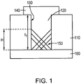
- Méthode de formation d'une structure, la méthode comprenant les étapes suivantes :pourvoir un substrat semi-conducteur cristallin (100) comprenant un premier matériau semi-conducteur et possédant une surface supérieure ;former un masque (1010) sur une surface supérieure du substrat semi-conducteur cristallin, et définir une ouverture de masque (1000) dans le masque pour exposer une partie de la surface supérieure du substrat semi-conducteur cristallin ;effectuer une gravure sélective pour exposer un plan de cristal spécifique du substrat semi-conducteur cristallin dans une partie inférieure de l'ouverture de masque ;enlever le masque ;définir une couche non cristalline (110) au-dessus du substrat semi-conducteur cristallin obtenu aux étapes précédentes ;définir une ouverture (120) formée dans la couche non cristalline, possédant une paroi latérale non cristalline et étant formée par un procédé d'enlèvement sélectif, de sorte d'une part que l'ouverture se termine à la surface supérieure du substrat semi-conducteur cristallin pour révéler le plan de cristal spécifique exposé précédemment, d'autre part que la paroi latérale non cristalline de l'ouverture définisse un angle inférieur à 90° avec le plan de cristal exposé ;former une pellicule épitaxiale (140) dans l'ouverture, la pellicule épitaxiale comprenant un deuxième matériau semi-conducteur et incluant un front de croissance, le front de croissance comportant une surface comprenant une facette non parallèle à la surface supérieure, et la surface définissant environ le même angle avec la paroi latérale non cristalline de l'ouverture, le deuxième matériau semi-conducteur étant à réseau désaccordé avec le premier matériau semi-conducteur,des dislocations (150) dans la pellicule épitaxiale étant dirigées dans une direction substantiellement perpendiculaire au front de croissance, de sorte que les dislocations sont coincées par la paroi latérale non cristalline de l'ouverture.
- Méthode selon la revendication 1, la paroi latérale non cristalline comprenant une paroi latérale diélectrique.
- Méthode selon la revendication 1, l'ouverture comprenant un sillon.
- Méthode selon la revendication 1, le premier matériau semi-conducteur comprenant un élément du groupe IV, et le deuxième matériau semi-conducteur comprenant au moins un d'un élément ou composé du groupe IV, un composé III-V, ou un composé II-VI.
- Méthode selon la revendication 4, le deuxième matériau semi-conducteur comprenant le composé III-V, et le composé III-V comprenant au moins un de AlP, GaP, InP, AlAs, GaAs, InAs, AlSb, GaSb, InSb, AlN, GaN, InN, ou leurs composés ternaires ou quaternaires.
- Méthode selon la revendication 3, le sillon mesurant au moins 6 mm de long.
- Méthode selon la revendication 3, le sillon mesurant moins de 400 nm de large.
- Méthode selon une quelconque des revendications précédentes, le deuxième matériau semi-conducteur comprenant une première couche développée à un premier jeu de conditions de traitement, et une deuxième couche disposée au-dessus de la première couche, et développée à un deuxième jeu de conditions de traitement.
- Méthode selon une quelconque des revendications précédentes, comprenant en outre : la formation d'un transistor, le transistor comprenant au moins une partie du deuxième matériau semi-conducteur.
- Méthode selon une quelconque des revendications précédentes, comprenant en outre : la formation d'un dispositif optoélectronique, le dispositif optoélectronique comprenant au moins une partie du deuxième matériau semi-conducteur.
Applications Claiming Priority (3)
| Application Number | Priority Date | Filing Date | Title |
|---|---|---|---|
| US84277106P | 2006-09-07 | 2006-09-07 | |
| US87390306P | 2006-12-08 | 2006-12-08 | |
| PCT/US2007/019568 WO2008030574A1 (fr) | 2006-09-07 | 2007-09-07 | Réduction des défauts par piégeage basé sur le rapport de forme |
Publications (2)
| Publication Number | Publication Date |
|---|---|
| EP2062290A1 EP2062290A1 (fr) | 2009-05-27 |
| EP2062290B1 true EP2062290B1 (fr) | 2019-08-28 |
Family
ID=38961470
Family Applications (1)
| Application Number | Title | Priority Date | Filing Date |
|---|---|---|---|
| EP07837902.1A Active EP2062290B1 (fr) | 2006-09-07 | 2007-09-07 | Réduction des défauts par piégeage basé sur le rapport de forme |
Country Status (3)
| Country | Link |
|---|---|
| US (4) | US8173551B2 (fr) |
| EP (1) | EP2062290B1 (fr) |
| WO (1) | WO2008030574A1 (fr) |
Families Citing this family (129)
| Publication number | Priority date | Publication date | Assignee | Title |
|---|---|---|---|---|
| WO2006125040A2 (fr) * | 2005-05-17 | 2006-11-23 | Amberwave Systems Corporation | Structures semi-conductrices en desaccord de maille possedant des densites de dislocations reduites et procedes associes de fabrication d'un dispositif |
| US8324660B2 (en) | 2005-05-17 | 2012-12-04 | Taiwan Semiconductor Manufacturing Company, Ltd. | Lattice-mismatched semiconductor structures with reduced dislocation defect densities and related methods for device fabrication |
| US9153645B2 (en) | 2005-05-17 | 2015-10-06 | Taiwan Semiconductor Manufacturing Company, Ltd. | Lattice-mismatched semiconductor structures with reduced dislocation defect densities and related methods for device fabrication |
| WO2007014294A2 (fr) * | 2005-07-26 | 2007-02-01 | Amberwave Systems Corporation | Solutions permettant d'integrer des materiaux alternatifs dans des circuits integres |
| US20070054467A1 (en) * | 2005-09-07 | 2007-03-08 | Amberwave Systems Corporation | Methods for integrating lattice-mismatched semiconductor structure on insulators |
| US7638842B2 (en) * | 2005-09-07 | 2009-12-29 | Amberwave Systems Corporation | Lattice-mismatched semiconductor structures on insulators |
| WO2007112066A2 (fr) | 2006-03-24 | 2007-10-04 | Amberwave Systems Corporation | Structures semi-conductrices à désaccord de réseau et procédés de fabrication de dispositif associés |
| US8173551B2 (en) | 2006-09-07 | 2012-05-08 | Taiwan Semiconductor Manufacturing Co., Ltd. | Defect reduction using aspect ratio trapping |
| US20080070355A1 (en) * | 2006-09-18 | 2008-03-20 | Amberwave Systems Corporation | Aspect ratio trapping for mixed signal applications |
| US7799592B2 (en) | 2006-09-27 | 2010-09-21 | Taiwan Semiconductor Manufacturing Company, Ltd. | Tri-gate field-effect transistors formed by aspect ratio trapping |
| US7875958B2 (en) | 2006-09-27 | 2011-01-25 | Taiwan Semiconductor Manufacturing Company, Ltd. | Quantum tunneling devices and circuits with lattice-mismatched semiconductor structures |
| US7498265B2 (en) * | 2006-10-04 | 2009-03-03 | Micron Technology, Inc. | Epitaxial silicon growth |
| WO2008051503A2 (fr) | 2006-10-19 | 2008-05-02 | Amberwave Systems Corporation | Dispositifs base sur une source de lumière munie de structures semi-conductrices a désaccord de réseau |
| US7825328B2 (en) | 2007-04-09 | 2010-11-02 | Taiwan Semiconductor Manufacturing Company, Ltd. | Nitride-based multi-junction solar cell modules and methods for making the same |
| US8304805B2 (en) | 2009-01-09 | 2012-11-06 | Taiwan Semiconductor Manufacturing Company, Ltd. | Semiconductor diodes fabricated by aspect ratio trapping with coalesced films |
| US9508890B2 (en) | 2007-04-09 | 2016-11-29 | Taiwan Semiconductor Manufacturing Company, Ltd. | Photovoltaics on silicon |
| US8237151B2 (en) | 2009-01-09 | 2012-08-07 | Taiwan Semiconductor Manufacturing Company, Ltd. | Diode-based devices and methods for making the same |
| US8329541B2 (en) | 2007-06-15 | 2012-12-11 | Taiwan Semiconductor Manufacturing Company, Ltd. | InP-based transistor fabrication |
| DE112008002387B4 (de) | 2007-09-07 | 2022-04-07 | Taiwan Semiconductor Manufacturing Co., Ltd. | Struktur einer Mehrfachübergangs-Solarzelle, Verfahren zur Bildung einer photonischenVorrichtung, Photovoltaische Mehrfachübergangs-Zelle und Photovoltaische Mehrfachübergangs-Zellenvorrichtung, |
| US8183667B2 (en) * | 2008-06-03 | 2012-05-22 | Taiwan Semiconductor Manufacturing Co., Ltd. | Epitaxial growth of crystalline material |
| US8274097B2 (en) | 2008-07-01 | 2012-09-25 | Taiwan Semiconductor Manufacturing Company, Ltd. | Reduction of edge effects from aspect ratio trapping |
| US20100006961A1 (en) * | 2008-07-09 | 2010-01-14 | Analog Devices, Inc. | Recessed Germanium (Ge) Diode |
| US8981427B2 (en) * | 2008-07-15 | 2015-03-17 | Taiwan Semiconductor Manufacturing Company, Ltd. | Polishing of small composite semiconductor materials |
| US8304785B2 (en) * | 2008-07-29 | 2012-11-06 | Industrial Technology Research Institute | LED structure, manufacturing method thereof and LED module |
| WO2010033813A2 (fr) | 2008-09-19 | 2010-03-25 | Amberwave System Corporation | Formation de dispositifs par sur-croissance de couches epitaxiales |
| US8253211B2 (en) | 2008-09-24 | 2012-08-28 | Taiwan Semiconductor Manufacturing Company, Ltd. | Semiconductor sensor structures with reduced dislocation defect densities |
| CN102379046B (zh) | 2009-04-02 | 2015-06-17 | 台湾积体电路制造股份有限公司 | 从晶体材料的非极性平面形成的器件及其制作方法 |
| US8338884B2 (en) | 2009-05-12 | 2012-12-25 | Taiwan Semiconductor Manufacturing Company, Ltd. | Selective epitaxial growth of semiconductor materials with reduced defects |
| US8212287B2 (en) * | 2009-09-18 | 2012-07-03 | Palo Alto Research Center Incorporated | Nitride semiconductor structure and method of making same |
| US9601328B2 (en) * | 2009-10-08 | 2017-03-21 | Taiwan Semiconductor Manufacturing Company, Ltd. | Growing a III-V layer on silicon using aligned nano-scale patterns |
| EP2743981A1 (fr) * | 2009-10-30 | 2014-06-18 | Imec | Procédé de fabrication d'une structure de substrat à semi-conducteur intégré |
| US8242510B2 (en) * | 2010-01-28 | 2012-08-14 | Intersil Americas Inc. | Monolithic integration of gallium nitride and silicon devices and circuits, structure and method |
| TWI562195B (en) | 2010-04-27 | 2016-12-11 | Pilegrowth Tech S R L | Dislocation and stress management by mask-less processes using substrate patterning and methods for device fabrication |
| US8247249B2 (en) * | 2010-06-01 | 2012-08-21 | Palo Alto Research Center Incorporated | Semi-polar nitride-based light emitting structure and method of forming same |
| US8609517B2 (en) * | 2010-06-11 | 2013-12-17 | Taiwan Semiconductor Manufacturing Company, Ltd. | MOCVD for growing III-V compound semiconductors on silicon substrates |
| US8062963B1 (en) | 2010-10-08 | 2011-11-22 | Taiwan Semiconductor Manufacturing Company, Ltd. | Method of fabricating a semiconductor device having an epitaxy region |
| KR101205037B1 (ko) * | 2011-02-28 | 2012-11-26 | 에스케이하이닉스 주식회사 | 반도체 소자 및 그 형성방법 |
| US8445363B2 (en) * | 2011-04-21 | 2013-05-21 | United Microelectronics Corp. | Method of fabricating an epitaxial layer |
| KR101867999B1 (ko) | 2011-10-31 | 2018-06-18 | 삼성전자주식회사 | Iii-v족 물질층을 형성하는 방법, iii-v족 물질층을 포함하는 반도체 소자 및 그 제조방법 |
| US9559099B2 (en) | 2012-03-01 | 2017-01-31 | Taiwan Semiconductor Manufacturing Company, Ltd. | Apparatus and method for FinFETs |
| US8742509B2 (en) | 2012-03-01 | 2014-06-03 | Taiwan Semiconductor Manufacturing Company, Ltd. | Apparatus and method for FinFETs |
| US8836016B2 (en) | 2012-03-08 | 2014-09-16 | Taiwan Semiconductor Manufacturing Company, Ltd. | Semiconductor structures and methods with high mobility and high energy bandgap materials |
| US9876129B2 (en) * | 2012-05-10 | 2018-01-23 | International Business Machines Corporation | Cone-shaped holes for high efficiency thin film solar cells |
| US8680576B2 (en) | 2012-05-16 | 2014-03-25 | Taiwan Semiconductor Manufacturing Company, Ltd. | CMOS device and method of forming the same |
| US9142400B1 (en) | 2012-07-17 | 2015-09-22 | Stc.Unm | Method of making a heteroepitaxial layer on a seed area |
| EP2717316B1 (fr) * | 2012-10-05 | 2019-08-14 | IMEC vzw | Procédé de production de structures à ailettes contraintes de germanium |
| US8841177B2 (en) | 2012-11-15 | 2014-09-23 | International Business Machines Corporation | Co-integration of elemental semiconductor devices and compound semiconductor devices |
| WO2014140082A1 (fr) | 2013-03-13 | 2014-09-18 | Pilegrowth Tech S.R.L. | Cellules solaires à rendement élevé sur substrats en silicium |
| US20140342533A1 (en) * | 2013-05-15 | 2014-11-20 | Applied Materials, Inc. | Method of strain and defect control in thin semiconductor films |
| US9748429B1 (en) * | 2013-06-11 | 2017-08-29 | National Technology & Engineering Solutions Of Sandia, Llc | Avalanche diode having reduced dark current and method for its manufacture |
| US9356147B2 (en) * | 2013-06-14 | 2016-05-31 | Globalfoundries Inc. | FinFET spacer etch for eSiGe improvement |
| US9330908B2 (en) | 2013-06-25 | 2016-05-03 | Globalfoundries Inc. | Semiconductor structure with aspect ratio trapping capabilities |
| US20150048422A1 (en) * | 2013-08-16 | 2015-02-19 | International Business Machines Corporation | A method for forming a crystalline compound iii-v material on a single element substrate |
| GB2517697A (en) | 2013-08-27 | 2015-03-04 | Ibm | Compound semiconductor structure |
| US8999779B2 (en) | 2013-09-06 | 2015-04-07 | International Business Machines Corporation | Locally raised epitaxy for improved contact by local silicon capping during trench silicide processings |
| FR3010828B1 (fr) * | 2013-09-13 | 2015-09-25 | Commissariat Energie Atomique | Procede optimise de fabrication de motifs de materiau semiconducteur iii-v sur un substrat semiconducteur |
| JP5957771B2 (ja) * | 2013-10-11 | 2016-07-27 | パナソニックIpマネジメント株式会社 | 窒化物半導体積層構造、半導体発光素子および窒化物半導体積層構造を製造する方法 |
| KR102104062B1 (ko) | 2013-10-31 | 2020-04-23 | 삼성전자 주식회사 | 기판 구조체, 이를 포함한 cmos 소자 및 cmos 소자 제조 방법 |
| US9177967B2 (en) | 2013-12-24 | 2015-11-03 | Intel Corporation | Heterogeneous semiconductor material integration techniques |
| KR102168969B1 (ko) * | 2014-02-28 | 2020-10-22 | 삼성전자주식회사 | 반도체 장치 및 그 제조 방법 |
| KR20150104420A (ko) | 2014-03-05 | 2015-09-15 | 삼성전자주식회사 | 반도체 소자 및 그의 제조 방법 |
| US9064698B1 (en) | 2014-03-30 | 2015-06-23 | International Business Machines Corporation | Thin-film gallium nitride structures grown on graphene |
| US9287123B2 (en) | 2014-04-28 | 2016-03-15 | Varian Semiconductor Equipment Associates, Inc. | Techniques for forming angled structures for reduced defects in heteroepitaxy of semiconductor films |
| JP6211999B2 (ja) * | 2014-06-25 | 2017-10-11 | 株式会社東芝 | 窒化物半導体層、窒化物半導体装置及び窒化物半導体層の製造方法 |
| US9601583B2 (en) * | 2014-07-15 | 2017-03-21 | Armonk Business Machines Corporation | Hetero-integration of III-N material on silicon |
| JP2017533574A (ja) | 2014-09-18 | 2017-11-09 | インテル・コーポレーション | シリコンcmos互換性半導体装置における欠陥伝播制御のための傾斜側壁カット面を有するウルツ鉱ヘテロエピタキシャル構造物 |
| KR102203497B1 (ko) | 2014-09-25 | 2021-01-15 | 인텔 코포레이션 | 독립형 실리콘 메사들 상의 iii-n 에피택셜 디바이스 구조체들 |
| EP3018715A1 (fr) | 2014-11-05 | 2016-05-11 | IMEC vzw | Procédé de fabrication d'un dispositif de transistor comprenant un matériau de canal de germanium sur un substrat à base de silicium et dispositif à transistor associé |
| US9349594B1 (en) | 2014-11-05 | 2016-05-24 | International Business Machines Corporation | Non-planar semiconductor device with aspect ratio trapping |
| US9293530B1 (en) | 2014-11-14 | 2016-03-22 | International Business Machines Corporation | High aspect ratio trapping semiconductor with uniform height and isolated from bulk substrate |
| US9349809B1 (en) | 2014-11-14 | 2016-05-24 | International Business Machines Corporation | Aspect ratio trapping and lattice engineering for III/V semiconductors |
| EP3221886A4 (fr) | 2014-11-18 | 2018-07-11 | Intel Corporation | Circuits cmos utilisant des transistors au nitrure de gallium à canal n et à canal p |
| US10056456B2 (en) | 2014-12-18 | 2018-08-21 | Intel Corporation | N-channel gallium nitride transistors |
| US9601565B2 (en) * | 2014-12-22 | 2017-03-21 | Globalfoundries Inc. | Zig-zag trench structure to prevent aspect ratio trapping defect escape |
| CN107004713B (zh) * | 2014-12-24 | 2021-02-09 | 英特尔公司 | 形成具有非对称外形的鳍状物结构的装置和方法 |
| US9379184B1 (en) * | 2015-02-18 | 2016-06-28 | International Business Machines Corporation | Secure chip with physically unclonable function |
| US9548319B2 (en) | 2015-03-10 | 2017-01-17 | International Business Machines Corporation | Structure for integration of an III-V compound semiconductor on SOI |
| US9608067B2 (en) | 2015-03-30 | 2017-03-28 | International Business Machines Corporation | Hybrid aspect ratio trapping |
| US9443940B1 (en) | 2015-04-07 | 2016-09-13 | Globalfoundries Inc. | Defect reduction with rotated double aspect ratio trapping |
| CN107949914B (zh) | 2015-05-19 | 2022-01-18 | 英特尔公司 | 具有凸起掺杂晶体结构的半导体器件 |
| US9590107B2 (en) | 2015-06-25 | 2017-03-07 | International Business Machines Corporation | III-V gate-all-around field effect transistor using aspect ratio trapping |
| KR102349040B1 (ko) | 2015-06-26 | 2022-01-10 | 인텔 코포레이션 | 고온 안정 기판 계면 재료를 갖는 헤테로 에피택셜 구조체들 |
| EP3125273A1 (fr) | 2015-07-31 | 2017-02-01 | IMEC vzw | Canaux du groupe iv contraints |
| US9916985B2 (en) | 2015-10-14 | 2018-03-13 | International Business Machines Corporation | Indium phosphide smoothing and chemical mechanical planarization processes |
| US9646842B1 (en) | 2015-10-14 | 2017-05-09 | International Business Machines Corporation | Germanium smoothing and chemical mechanical planarization processes |
| US9646841B1 (en) | 2015-10-14 | 2017-05-09 | International Business Machines Corporation | Group III arsenide material smoothing and chemical mechanical planarization processes |
| KR102379701B1 (ko) | 2015-10-19 | 2022-03-28 | 삼성전자주식회사 | 멀티-채널을 갖는 반도체 소자 및 그 형성 방법 |
| US9564494B1 (en) * | 2015-11-18 | 2017-02-07 | International Business Machines Corporation | Enhanced defect reduction for heteroepitaxy by seed shape engineering |
| US9570443B1 (en) * | 2015-11-23 | 2017-02-14 | International Business Machines Corporation | Field effect transistor including strained germanium fins |
| JP6706414B2 (ja) * | 2015-11-27 | 2020-06-10 | 国立研究開発法人情報通信研究機構 | Ge単結晶薄膜の製造方法及び光デバイス |
| US9601482B1 (en) | 2015-12-08 | 2017-03-21 | International Business Machines Corporation | Economical and environmentally friendly chemical mechanical polishing for III-V compound semiconductor device fabrication |
| US9570297B1 (en) * | 2015-12-09 | 2017-02-14 | International Business Machines Corporation | Elimination of defects in long aspect ratio trapping trench structures |
| WO2017111869A1 (fr) | 2015-12-24 | 2017-06-29 | Intel Corporation | Dichalcogénures de métaux de transition (tmdc) sur couches hétéroépitaxiales de nitrures du groupe iii |
| WO2017111873A1 (fr) * | 2015-12-26 | 2017-06-29 | Intel Corporation | Procédé d'obtention d'une couche de matériau du groupe iv uniforme dans une tranchée de piégeage par rapport de forme |
| KR102430501B1 (ko) | 2015-12-29 | 2022-08-09 | 삼성전자주식회사 | 반도체 단결정구조, 반도체 디바이스 및 그 제조방법 |
| US9437427B1 (en) * | 2015-12-30 | 2016-09-06 | International Business Machines Corporation | Controlled confined lateral III-V epitaxy |
| US9564452B1 (en) | 2016-02-01 | 2017-02-07 | International Business Machines Corporation | Fabrication of hybrid semiconductor circuits |
| US9704757B1 (en) | 2016-02-25 | 2017-07-11 | International Business Machines Corporation | Fabrication of semiconductor structures |
| DE112016006664T5 (de) * | 2016-03-30 | 2018-12-20 | Intel Corporation | Ätzen eines gratkerns, um eine gratverdoppelung vorzusehen |
| US9735010B1 (en) | 2016-05-27 | 2017-08-15 | International Business Machines Corporation | Fabrication of semiconductor fin structures |
| US10249492B2 (en) | 2016-05-27 | 2019-04-02 | International Business Machines Corporation | Fabrication of compound semiconductor structures |
| US10181526B2 (en) | 2016-06-02 | 2019-01-15 | Samsung Electronics Co., Ltd. | Field effect transistor including multiple aspect ratio trapping structures |
| US11158714B2 (en) * | 2016-06-09 | 2021-10-26 | Intel Corporation | Quantum dot devices with trenched substrates |
| US10636912B2 (en) | 2016-06-30 | 2020-04-28 | Intel Corporation | FINFET transistor having a tapered subfin structure |
| US10243063B2 (en) | 2016-07-29 | 2019-03-26 | Applied Materials, Inc. | Method of uniform channel formation |
| US9728626B1 (en) | 2016-08-30 | 2017-08-08 | Globalfoundries Inc. | Almost defect-free active channel region |
| US10978590B2 (en) | 2016-09-30 | 2021-04-13 | Intel Corporation | Methods and apparatus to remove epitaxial defects in semiconductors |
| US9947793B1 (en) | 2017-02-08 | 2018-04-17 | Globalfoundries Inc. | Vertical pillar-type field effect transistor and method |
| JP2018147396A (ja) * | 2017-03-08 | 2018-09-20 | 株式会社ジャパンディスプレイ | 表示装置 |
| US10032663B1 (en) * | 2017-05-24 | 2018-07-24 | Texas Instruments Incorporated | Anneal after trench sidewall implant to reduce defects |
| WO2019066885A1 (fr) | 2017-09-29 | 2019-04-04 | Intel Corporation | Couche de canal amélioré formée dans une technique de tranchée |
| WO2019066953A1 (fr) | 2017-09-29 | 2019-04-04 | Intel Corporation | Dispositifs à nitrure du groupe iii (iii-n) à résistance de contact réduite et leurs procédés de fabrication |
| US10944049B2 (en) * | 2017-11-13 | 2021-03-09 | Taiwan Semiconductor Manufacturing Company, Ltd. | MTJ device performance by controlling device shape |
| DE102018125373A1 (de) * | 2017-11-22 | 2019-05-23 | Taiwan Semiconductor Manufacturing Co., Ltd. | Verfahren zur Bildung eines SOI-Substrats |
| US10304723B1 (en) | 2017-11-22 | 2019-05-28 | Taiwan Semiconductor Manufacturing Co., Ltd. | Process to form SOI substrate |
| US10672889B2 (en) * | 2017-11-30 | 2020-06-02 | Taiwan Semiconductor Manufacturing Co., Ltd. | Semiconductor device and manufacturing method thereof |
| FR3075461B1 (fr) | 2017-12-20 | 2020-02-14 | Commissariat A L'energie Atomique Et Aux Energies Alternatives | Procede de fabrication d'une heterostructure comportant des structures elementaires photoniques en materiau iii-v a la surface d'un substrat a base de silicium |
| US10424653B1 (en) | 2018-05-21 | 2019-09-24 | International Business Machines Corporation | Vertical transport field effect transistor on silicon with defined junctions |
| US10580966B1 (en) | 2018-09-07 | 2020-03-03 | International Business Machines Corporation | Faceted sidewall magnetic tunnel junction structure |
| US10840093B2 (en) | 2018-09-11 | 2020-11-17 | International Business Machines Corporation | Fabrication of semiconductor substrates |
| US10366884B1 (en) * | 2018-11-08 | 2019-07-30 | Stratio | Methods for forming a germanium island using selective epitaxial growth and a sacrificial filling layer |
| EP3828918A1 (fr) * | 2019-11-29 | 2021-06-02 | Imec VZW | Transistor bipolaire à hétérojonction de type ccb faiblement parasitaire |
| US10930490B1 (en) | 2019-12-26 | 2021-02-23 | Wisconsin Alumni Research Foundation | Arrays of high-aspect-ratio germanium nanostructures with nanoscale pitch and methods for the fabrication thereof |
| US11742203B2 (en) * | 2020-02-26 | 2023-08-29 | The Hong Kong University Of Science And Technology | Method for growing III-V compound semiconductor thin films on silicon-on-insulators |
| US20220139709A1 (en) * | 2020-11-05 | 2022-05-05 | International Business Machines Corporation | Confined gallium nitride epitaxial layers |
| KR102532540B1 (ko) * | 2021-01-28 | 2023-05-17 | 한국과학기술연구원 | 3차원 적층 구조의 상부층으로의 스레딩 변전위의 전파가 억제되는 트렌치 구조를 갖는 반도체 소자 |
| CN117157732A (zh) * | 2021-04-15 | 2023-12-01 | 苏州晶湛半导体有限公司 | 半导体结构及其制作方法 |
| CN117063291A (zh) * | 2021-04-15 | 2023-11-14 | 苏州晶湛半导体有限公司 | 半导体结构及其制备方法 |
| CN117096208B (zh) * | 2023-10-20 | 2024-02-09 | 浙桂(杭州)半导体科技有限责任公司 | 一种锗硅雪崩光电二极管 |
Citations (2)
| Publication number | Priority date | Publication date | Assignee | Title |
|---|---|---|---|---|
| WO2006125040A2 (fr) * | 2005-05-17 | 2006-11-23 | Amberwave Systems Corporation | Structures semi-conductrices en desaccord de maille possedant des densites de dislocations reduites et procedes associes de fabrication d'un dispositif |
| WO2007112066A2 (fr) * | 2006-03-24 | 2007-10-04 | Amberwave Systems Corporation | Structures semi-conductrices à désaccord de réseau et procédés de fabrication de dispositif associés |
Family Cites Families (442)
| Publication number | Priority date | Publication date | Assignee | Title |
|---|---|---|---|---|
| SE391122B (sv) * | 1971-01-25 | 1977-02-07 | Cutter Lab | Protes i form av en ryggradsbroskskiva och forfarande for framstellning derav |
| US4307510A (en) | 1980-03-12 | 1981-12-29 | The United States Of America As Represented By The Administrator Of The National Aeronautics & Space Administration | Computer circuit card puller |
| WO1981002948A1 (fr) * | 1980-04-10 | 1981-10-15 | Massachusetts Inst Technology | Procede de production de feuilles d'un materiau cristallin et dispositifs fabriques a partir de ces feuilles |
| US4322253A (en) | 1980-04-30 | 1982-03-30 | Rca Corporation | Method of making selective crystalline silicon regions containing entrapped hydrogen by laser treatment |
| US4370510A (en) | 1980-09-26 | 1983-01-25 | California Institute Of Technology | Gallium arsenide single crystal solar cell structure and method of making |
| US4309777A (en) * | 1980-11-13 | 1982-01-12 | Patil Arun A | Artificial intervertebral disc |
| US4651179A (en) | 1983-01-21 | 1987-03-17 | Rca Corporation | Low resistance gallium arsenide field effect transistor |
| US4545109A (en) | 1983-01-21 | 1985-10-08 | Rca Corporation | Method of making a gallium arsenide field effect transistor |
| US5091333A (en) * | 1983-09-12 | 1992-02-25 | Massachusetts Institute Of Technology | Reducing dislocations in semiconductors utilizing repeated thermal cycling during multistage epitaxial growth |
| US4860081A (en) * | 1984-06-28 | 1989-08-22 | Gte Laboratories Incorporated | Semiconductor integrated circuit structure with insulative partitions |
| US4551394A (en) | 1984-11-26 | 1985-11-05 | Honeywell Inc. | Integrated three-dimensional localized epitaxial growth of Si with localized overgrowth of GaAs |
| EP0214610B1 (fr) | 1985-09-03 | 1990-12-05 | Daido Tokushuko Kabushiki Kaisha | Galette semi-conductrice en arséniure de gallium épitaxial et méthode pour la produire |
| US4774205A (en) * | 1986-06-13 | 1988-09-27 | Massachusetts Institute Of Technology | Monolithic integration of silicon and gallium arsenide devices |
| JPS63149021A (ja) | 1986-07-25 | 1988-06-21 | Dai Ichi High Frequency Co Ltd | 内管挿入方式による二重管ベンドの製造方法及び装置 |
| JPS6381855A (ja) | 1986-09-25 | 1988-04-12 | Mitsubishi Electric Corp | ヘテロ接合バイポ−ラトランジスタの製造方法 |
| CH671691A5 (fr) * | 1987-01-08 | 1989-09-29 | Sulzer Ag | |
| US5269876A (en) | 1987-01-26 | 1993-12-14 | Canon Kabushiki Kaisha | Process for producing crystal article |
| US5236546A (en) | 1987-01-26 | 1993-08-17 | Canon Kabushiki Kaisha | Process for producing crystal article |
| CA1283501C (fr) * | 1987-02-12 | 1991-04-30 | Thomas P. Hedman | Disque artificiel pour colonne vertebrale |
| US5281283A (en) | 1987-03-26 | 1994-01-25 | Canon Kabushiki Kaisha | Group III-V compound crystal article using selective epitaxial growth |
| US5166767A (en) | 1987-04-14 | 1992-11-24 | National Semiconductor Corporation | Sidewall contact bipolar transistor with controlled lateral spread of selectively grown epitaxial layer |
| US4957992A (en) * | 1987-04-21 | 1990-09-18 | Kao Corporation | Hair cosmetic composition |
| US4876210A (en) | 1987-04-30 | 1989-10-24 | The University Of Delaware | Solution growth of lattice mismatched and solubility mismatched heterostructures |
| US4826784A (en) * | 1987-11-13 | 1989-05-02 | Kopin Corporation | Selective OMCVD growth of compound semiconductor materials on silicon substrates |
| US5272105A (en) | 1988-02-11 | 1993-12-21 | Gte Laboratories Incorporated | Method of manufacturing an heteroepitaxial semiconductor structure |
| US5079616A (en) | 1988-02-11 | 1992-01-07 | Gte Laboratories Incorporated | Semiconductor structure |
| GB2215514A (en) | 1988-03-04 | 1989-09-20 | Plessey Co Plc | Terminating dislocations in semiconductor epitaxial layers |
| US5032893A (en) | 1988-04-01 | 1991-07-16 | Cornell Research Foundation, Inc. | Method for reducing or eliminating interface defects in mismatched semiconductor eiplayers |
| US5156995A (en) | 1988-04-01 | 1992-10-20 | Cornell Research Foundation, Inc. | Method for reducing or eliminating interface defects in mismatched semiconductor epilayers |
| DE8807485U1 (fr) * | 1988-06-06 | 1989-08-10 | Mecron Medizinische Produkte Gmbh, 1000 Berlin, De | |
| US4911718A (en) * | 1988-06-10 | 1990-03-27 | University Of Medicine & Dentistry Of N.J. | Functional and biocompatible intervertebral disc spacer |
| CA1333209C (fr) * | 1988-06-28 | 1994-11-29 | Gary Karlin Michelson | Implants artificiels pour la soudure osseuse intervertebrale |
| EP0352472A3 (fr) | 1988-07-25 | 1991-02-06 | Texas Instruments Incorporated | Hétéroépitaxie de matériaux semiconducteurs à résaux inégaux |
| US5238869A (en) | 1988-07-25 | 1993-08-24 | Texas Instruments Incorporated | Method of forming an epitaxial layer on a heterointerface |
| US5545229A (en) * | 1988-08-18 | 1996-08-13 | University Of Medicine And Dentistry Of Nj | Functional and biocompatible intervertebral disc spacer containing elastomeric material of varying hardness |
| JPH0262090A (ja) | 1988-08-29 | 1990-03-01 | Matsushita Electric Ind Co Ltd | 光半導体装置の製造方法 |
| US5061644A (en) | 1988-12-22 | 1991-10-29 | Honeywell Inc. | Method for fabricating self-aligned semiconductor devices |
| EP0380815B1 (fr) | 1989-01-31 | 1994-05-25 | Agfa-Gevaert N.V. | Intégration de GaAs sur substrat de Si |
| US5034337A (en) | 1989-02-10 | 1991-07-23 | Texas Instruments Incorporated | Method of making an integrated circuit that combines multi-epitaxial power transistors with logic/analog devices |
| US4948456A (en) | 1989-06-09 | 1990-08-14 | Delco Electronics Corporation | Confined lateral selective epitaxial growth |
| US5256594A (en) | 1989-06-16 | 1993-10-26 | Intel Corporation | Masking technique for depositing gallium arsenide on silicon |
| US5098850A (en) | 1989-06-16 | 1992-03-24 | Canon Kabushiki Kaisha | Process for producing substrate for selective crystal growth, selective crystal growth process and process for producing solar battery by use of them |
| FR2659226B1 (fr) * | 1990-03-07 | 1992-05-29 | Jbs Sa | Prothese pour disques intervertebraux et ses instruments d'implantation. |
| US5093699A (en) | 1990-03-12 | 1992-03-03 | Texas A & M University System | Gate adjusted resonant tunnel diode device and method of manufacture |
| US5164359A (en) | 1990-04-20 | 1992-11-17 | Eaton Corporation | Monolithic integrated circuit having compound semiconductor layer epitaxially grown on ceramic substrate |
| KR930006934B1 (ko) * | 1990-06-23 | 1993-07-24 | 한국과학기술연구원 | 폴리에틸렌 섬유/비닐 에스테르 수지 복합재의 접착력 증진 방법 |
| US5158907A (en) | 1990-08-02 | 1992-10-27 | At&T Bell Laboratories | Method for making semiconductor devices with low dislocation defects |
| US5105247A (en) | 1990-08-03 | 1992-04-14 | Cavanaugh Marion E | Quantum field effect device with source extension region formed under a gate and between the source and drain regions |
| JP3202223B2 (ja) | 1990-11-27 | 2001-08-27 | 日本電気株式会社 | トランジスタの製造方法 |
| US5403751A (en) * | 1990-11-29 | 1995-04-04 | Canon Kabushiki Kaisha | Process for producing a thin silicon solar cell |
| US5223043A (en) | 1991-02-11 | 1993-06-29 | The United States Of America As Represented By The United States Department Of Energy | Current-matched high-efficiency, multijunction monolithic solar cells |
| US5091767A (en) * | 1991-03-18 | 1992-02-25 | At&T Bell Laboratories | Article comprising a lattice-mismatched semiconductor heterostructure |
| JPH04299569A (ja) | 1991-03-27 | 1992-10-22 | Nec Corp | Soisの製造方法及びトランジスタとその製造方法 |
| US5269852A (en) | 1991-05-27 | 1993-12-14 | Canon Kabushiki Kaisha | Crystalline solar cell and method for producing the same |
| JP3058954B2 (ja) | 1991-09-24 | 2000-07-04 | ローム株式会社 | 絶縁層の上に成長層を有する半導体装置の製造方法 |
| JP2773487B2 (ja) | 1991-10-15 | 1998-07-09 | 日本電気株式会社 | トンネルトランジスタ |
| JPH05121317A (ja) | 1991-10-24 | 1993-05-18 | Rohm Co Ltd | Soi構造形成方法 |
| FR2693364B1 (fr) * | 1992-07-07 | 1995-06-30 | Erpios Snc | Prothese intervertebrale permettant une stabilisation des contraintes rotatoires et de flexion-extension. |
| JP3286920B2 (ja) | 1992-07-10 | 2002-05-27 | 富士通株式会社 | 半導体装置の製造方法 |
| EP0600276B1 (fr) * | 1992-12-04 | 1998-08-05 | Siemens Aktiengesellschaft | Procédé de production d'une zone monocristalline limitée latéralement par épitaxie sélective et son utilisation pour produire un transistor bipolaire ainsi qu'un transistor MOS |
| JP3319472B2 (ja) | 1992-12-07 | 2002-09-03 | 富士通株式会社 | 半導体装置とその製造方法 |
| US5295150A (en) * | 1992-12-11 | 1994-03-15 | Eastman Kodak Company | Distributed feedback-channeled substrate planar semiconductor laser |
| US5456722A (en) * | 1993-01-06 | 1995-10-10 | Smith & Nephew Richards Inc. | Load bearing polymeric cable |
| US5407491A (en) | 1993-04-08 | 1995-04-18 | University Of Houston | Tandem solar cell with improved tunnel junction |
| EP0627799B1 (fr) * | 1993-06-04 | 1997-10-08 | Sharp Kabushiki Kaisha | Dispositif semi-conducteur émettant de la lumière avec une troisième couche de gaine |
| JP3748905B2 (ja) | 1993-08-27 | 2006-02-22 | 三洋電機株式会社 | 量子効果デバイス |
| US5792679A (en) | 1993-08-30 | 1998-08-11 | Sharp Microelectronics Technology, Inc. | Method for forming silicon-germanium/Si/silicon dioxide heterostructure using germanium implant |
| US5461243A (en) | 1993-10-29 | 1995-10-24 | International Business Machines Corporation | Substrate for tensilely strained semiconductor |
| US5405453A (en) | 1993-11-08 | 1995-04-11 | Applied Solar Energy Corporation | High efficiency multi-junction solar cell |
| US5489539A (en) | 1994-01-10 | 1996-02-06 | Hughes Aircraft Company | Method of making quantum well structure with self-aligned gate |
| US5458642A (en) * | 1994-01-18 | 1995-10-17 | Beer; John C. | Synthetic intervertebral disc |
| JPH07230952A (ja) | 1994-02-16 | 1995-08-29 | Ricoh Co Ltd | 再結晶化方法 |
| JPH0851109A (ja) | 1994-04-11 | 1996-02-20 | Texas Instr Inc <Ti> | 酸化物でパターン化されたウェーハの窓内にエピタキシャルシリコンを成長させる方法 |
| US6011271A (en) | 1994-04-28 | 2000-01-04 | Fujitsu Limited | Semiconductor device and method of fabricating the same |
| US5710436A (en) | 1994-09-27 | 1998-01-20 | Kabushiki Kaisha Toshiba | Quantum effect device |
| US5825240A (en) | 1994-11-30 | 1998-10-20 | Massachusetts Institute Of Technology | Resonant-tunneling transmission line technology |
| JP3835225B2 (ja) | 1995-02-23 | 2006-10-18 | 日亜化学工業株式会社 | 窒化物半導体発光素子 |
| US5528209A (en) | 1995-04-27 | 1996-06-18 | Hughes Aircraft Company | Monolithic microwave integrated circuit and method |
| JPH08306700A (ja) | 1995-04-27 | 1996-11-22 | Nec Corp | 半導体装置及びその製造方法 |
| TW304310B (fr) * | 1995-05-31 | 1997-05-01 | Siemens Ag | |
| US5621227A (en) | 1995-07-18 | 1997-04-15 | Discovery Semiconductors, Inc. | Method and apparatus for monolithic optoelectronic integrated circuit using selective epitaxy |
| KR100473901B1 (ko) | 1995-12-15 | 2005-08-29 | 코닌클리케 필립스 일렉트로닉스 엔.브이. | SiGe층을포함하는반도체전계효과디바이스 |
| TW314621B (fr) | 1995-12-20 | 1997-09-01 | Toshiba Co Ltd | |
| US5987590A (en) | 1996-04-02 | 1999-11-16 | Texas Instruments Incorporated | PC circuits, systems and methods |
| ZA974261B (en) | 1996-05-17 | 1997-11-17 | Canon Kk | Photovoltaic device and process for the production thereof. |
| JP3719618B2 (ja) | 1996-06-17 | 2005-11-24 | 松下電器産業株式会社 | 半導体装置及びその製造方法 |
| US6229153B1 (en) | 1996-06-21 | 2001-05-08 | Wisconsin Alumni Research Corporation | High peak current density resonant tunneling diode |
| JP3260660B2 (ja) | 1996-08-22 | 2002-02-25 | 株式会社東芝 | 半導体装置およびその製造方法 |
| JP3449516B2 (ja) | 1996-08-30 | 2003-09-22 | 株式会社リコー | 半導体多層膜反射鏡および半導体多層膜反射防止膜および面発光型半導体レーザおよび受光素子 |
| US6191432B1 (en) | 1996-09-02 | 2001-02-20 | Kabushiki Kaisha Toshiba | Semiconductor device and memory device |
| US5825049A (en) | 1996-10-09 | 1998-10-20 | Sandia Corporation | Resonant tunneling device with two-dimensional quantum well emitter and base layers |
| JPH10126010A (ja) | 1996-10-23 | 1998-05-15 | Ricoh Co Ltd | 半導体レーザ装置の製造方法 |
| SG65697A1 (en) * | 1996-11-15 | 1999-06-22 | Canon Kk | Process for producing semiconductor article |
| US5827328A (en) * | 1996-11-22 | 1998-10-27 | Buttermann; Glenn R. | Intervertebral prosthetic device |
| US5853497A (en) | 1996-12-12 | 1998-12-29 | Hughes Electronics Corporation | High efficiency multi-junction solar cells |
| US6348096B1 (en) | 1997-03-13 | 2002-02-19 | Nec Corporation | Method for manufacturing group III-V compound semiconductors |
| JP3853905B2 (ja) | 1997-03-18 | 2006-12-06 | 株式会社東芝 | 量子効果装置とblトンネル素子を用いた装置 |
| EP0874405A3 (fr) | 1997-03-25 | 2004-09-15 | Mitsubishi Cable Industries, Ltd. | Element à base de GaN avec une faible densité de dislocations, son utilisation et procédés de fabrication |
| JP3047852B2 (ja) | 1997-04-04 | 2000-06-05 | 松下電器産業株式会社 | 半導体装置 |
| CN1131548C (zh) | 1997-04-04 | 2003-12-17 | 松下电器产业株式会社 | 半导体装置 |
| JP3184115B2 (ja) | 1997-04-11 | 2001-07-09 | 松下電器産業株式会社 | オーミック電極形成方法 |
| ATE550461T1 (de) * | 1997-04-11 | 2012-04-15 | Nichia Corp | Wachstumsmethode für einen nitrid-halbleiter |
| US5998781A (en) | 1997-04-30 | 1999-12-07 | Sandia Corporation | Apparatus for millimeter-wave signal generation |
| US5903170A (en) | 1997-06-03 | 1999-05-11 | The Regents Of The University Of Michigan | Digital logic design using negative differential resistance diodes and field-effect transistors |
| US5883549A (en) | 1997-06-20 | 1999-03-16 | Hughes Electronics Corporation | Bipolar junction transistor (BJT)--resonant tunneling diode (RTD) oscillator circuit and method |
| KR100400808B1 (ko) * | 1997-06-24 | 2003-10-08 | 매사츄세츠 인스티튜트 오브 테크놀러지 | 그레이드된 GeSi층 및 평탄화를 사용한 Si상의 Ge의 쓰레딩 전위 밀도 제어 |
| US5869845A (en) | 1997-06-26 | 1999-02-09 | Texas Instruments Incorporated | Resonant tunneling memory |
| JP3930161B2 (ja) | 1997-08-29 | 2007-06-13 | 株式会社東芝 | 窒化物系半導体素子、発光素子及びその製造方法 |
| US6015979A (en) * | 1997-08-29 | 2000-01-18 | Kabushiki Kaisha Toshiba | Nitride-based semiconductor element and method for manufacturing the same |
| US20010006249A1 (en) * | 1997-09-16 | 2001-07-05 | Eugene A Fitzgerald | Co-planar si and ge composite substrate and method of producing same |
| FR2769924B1 (fr) | 1997-10-20 | 2000-03-10 | Centre Nat Rech Scient | Procede de realisation d'une couche epitaxiale de nitrure de gallium, couche epitaxiale de nitrure de gallium et composant optoelectronique muni d'une telle couche |
| DE69842052D1 (de) * | 1997-10-30 | 2011-01-27 | Sumitomo Electric Industries | Gan einkristall-substrat und herstellungsmethode |
| JP3180743B2 (ja) * | 1997-11-17 | 2001-06-25 | 日本電気株式会社 | 窒化化合物半導体発光素子およびその製法 |
| FR2772594B1 (fr) * | 1997-12-19 | 2000-05-05 | Henry Graf | Prothese discale partielle posterieure |
| US6258125B1 (en) * | 1998-08-03 | 2001-07-10 | Synthes (U.S.A.) | Intervertebral allograft spacer |
| FR2775183B1 (fr) * | 1998-02-20 | 2000-08-04 | Jean Taylor | Prothese inter-epineuse |
| JP3468082B2 (ja) | 1998-02-26 | 2003-11-17 | 日亜化学工業株式会社 | 窒化物半導体素子 |
| US6150242A (en) | 1998-03-25 | 2000-11-21 | Texas Instruments Incorporated | Method of growing crystalline silicon overlayers on thin amorphous silicon oxide layers and forming by method a resonant tunneling diode |
| JPH11274467A (ja) | 1998-03-26 | 1999-10-08 | Murata Mfg Co Ltd | 光電子集積回路素子 |
| US6500257B1 (en) | 1998-04-17 | 2002-12-31 | Agilent Technologies, Inc. | Epitaxial material grown laterally within a trench and method for producing same |
| JP3338778B2 (ja) | 1998-04-24 | 2002-10-28 | 日本電気株式会社 | 窒化物系化合物半導体レーザ素子 |
| US6265289B1 (en) * | 1998-06-10 | 2001-07-24 | North Carolina State University | Methods of fabricating gallium nitride semiconductor layers by lateral growth from sidewalls into trenches, and gallium nitride semiconductor structures fabricated thereby |
| US6527803B1 (en) * | 1998-06-23 | 2003-03-04 | Dimso (Distribution Medicale Du Sud-Ouest) | Intersomatic spine implant having anchoring elements |
| JP4005701B2 (ja) | 1998-06-24 | 2007-11-14 | シャープ株式会社 | 窒素化合物半導体膜の形成方法および窒素化合物半導体素子 |
| KR100580307B1 (ko) | 1998-07-14 | 2006-05-16 | 후지쯔 가부시끼가이샤 | 반도체 레이저 및 반도체 장치 |
| US6063121A (en) * | 1998-07-29 | 2000-05-16 | Xavier; Ravi | Vertebral body prosthesis |
| US6749635B1 (en) * | 1998-09-04 | 2004-06-15 | Sdgi Holdings, Inc. | Peanut spectacle multi discoid thoraco-lumbar disc prosthesis |
| EP1115163A4 (fr) | 1998-09-10 | 2001-12-05 | Rohm Co Ltd | Del a semi-conducteur et son procede de fabrication |
| US6252261B1 (en) | 1998-09-30 | 2001-06-26 | Nec Corporation | GaN crystal film, a group III element nitride semiconductor wafer and a manufacturing process therefor |
| FR2787014B1 (fr) * | 1998-12-11 | 2001-03-02 | Dimso Sa | Prothese de disque intervertebral a frottements reduits |
| FR2787015B1 (fr) * | 1998-12-11 | 2001-04-27 | Dimso Sa | Prothese de disque intervertebral a corps compressible |
| FR2787016B1 (fr) * | 1998-12-11 | 2001-03-02 | Dimso Sa | Prothese de disque intervertebral |
| JP3868136B2 (ja) | 1999-01-20 | 2007-01-17 | 日亜化学工業株式会社 | 窒化ガリウム系化合物半導体発光素子 |
| JP3372226B2 (ja) | 1999-02-10 | 2003-01-27 | 日亜化学工業株式会社 | 窒化物半導体レーザ素子 |
| AU2999900A (en) * | 1999-02-18 | 2000-09-04 | Ken Y. Hsu | Hair used as a biologic disk, replacement, and/or structure and method |
| US6113638A (en) * | 1999-02-26 | 2000-09-05 | Williams; Lytton A. | Method and apparatus for intervertebral implant anchorage |
| US7145167B1 (en) | 2000-03-11 | 2006-12-05 | International Business Machines Corporation | High speed Ge channel heterostructures for field effect devices |
| JP3760663B2 (ja) | 1999-03-31 | 2006-03-29 | 豊田合成株式会社 | Iii族窒化物系化合物半導体素子の製造方法 |
| JP3702700B2 (ja) * | 1999-03-31 | 2005-10-05 | 豊田合成株式会社 | Iii族窒化物系化合物半導体素子及びその製造方法 |
| DE10017137A1 (de) | 1999-04-14 | 2000-10-26 | Siemens Ag | Silizium-Aufbau und Verfahren zu dessen Herstellung |
| US6803598B1 (en) | 1999-05-07 | 2004-10-12 | University Of Delaware | Si-based resonant interband tunneling diodes and method of making interband tunneling diodes |
| JP3587081B2 (ja) | 1999-05-10 | 2004-11-10 | 豊田合成株式会社 | Iii族窒化物半導体の製造方法及びiii族窒化物半導体発光素子 |
| WO2000070683A1 (fr) | 1999-05-13 | 2000-11-23 | Hitachi, Ltd. | Mémoire à semi-conducteurs |
| US6252287B1 (en) | 1999-05-19 | 2001-06-26 | Sandia Corporation | InGaAsN/GaAs heterojunction for multi-junction solar cells |
| JP3555500B2 (ja) * | 1999-05-21 | 2004-08-18 | 豊田合成株式会社 | Iii族窒化物半導体及びその製造方法 |
| GB9912178D0 (en) | 1999-05-25 | 1999-07-28 | Univ Court Of The University O | Improved optical modulator |
| US6419704B1 (en) * | 1999-10-08 | 2002-07-16 | Bret Ferree | Artificial intervertebral disc replacement methods and apparatus |
| US20020128714A1 (en) * | 1999-06-04 | 2002-09-12 | Mark Manasas | Orthopedic implant and method of making metal articles |
| US6214653B1 (en) | 1999-06-04 | 2001-04-10 | International Business Machines Corporation | Method for fabricating complementary metal oxide semiconductor (CMOS) devices on a mixed bulk and silicon-on-insulator (SOI) substrate |
| EP1185221B1 (fr) * | 1999-06-04 | 2005-03-23 | SDGI Holdings, Inc. | Implant de disque artificiel |
| JP2001007447A (ja) | 1999-06-18 | 2001-01-12 | Nichia Chem Ind Ltd | 窒化物半導体レーザ素子 |
| US6635110B1 (en) | 1999-06-25 | 2003-10-21 | Massachusetts Institute Of Technology | Cyclic thermal anneal for dislocation reduction |
| US6228691B1 (en) | 1999-06-30 | 2001-05-08 | Intel Corp. | Silicon-on-insulator devices and method for producing the same |
| GB9919479D0 (en) | 1999-08-17 | 1999-10-20 | Imperial College | Island arrays |
| US6339232B1 (en) | 1999-09-20 | 2002-01-15 | Kabushika Kaisha Toshiba | Semiconductor device |
| US6447543B1 (en) * | 1999-09-28 | 2002-09-10 | Sulzer Orthopedics Ltd. | Basket-like container for implanting bone tissue |
| JP2001102678A (ja) | 1999-09-29 | 2001-04-13 | Toshiba Corp | 窒化ガリウム系化合物半導体素子 |
| US6264695B1 (en) * | 1999-09-30 | 2001-07-24 | Replication Medical, Inc. | Spinal nucleus implant |
| US6984571B1 (en) | 1999-10-01 | 2006-01-10 | Ziptronix, Inc. | Three dimensional device integration method and integrated device |
| FR2799638B1 (fr) * | 1999-10-14 | 2002-08-16 | Fred Zacouto | Fixateur et articulation vertebrale |
| US6812053B1 (en) | 1999-10-14 | 2004-11-02 | Cree, Inc. | Single step pendeo- and lateral epitaxial overgrowth of Group III-nitride epitaxial layers with Group III-nitride buffer layer and resulting structures |
| JP2001189483A (ja) | 1999-10-18 | 2001-07-10 | Sharp Corp | バイパス機能付太陽電池セルおよびバイパス機能付き多接合積層型太陽電池セルおよびそれらの製造方法 |
| DE60036594T2 (de) | 1999-11-15 | 2008-01-31 | Matsushita Electric Industrial Co., Ltd., Kadoma | Feldeffekt-Halbleiterbauelement |
| US6521514B1 (en) * | 1999-11-17 | 2003-02-18 | North Carolina State University | Pendeoepitaxial methods of fabricating gallium nitride semiconductor layers on sapphire substrates |
| JP2001176805A (ja) | 1999-12-16 | 2001-06-29 | Sony Corp | 窒化物系iii−v族化合物の結晶製造方法、窒化物系iii−v族化合物結晶基板、窒化物系iii−v族化合物結晶膜およびデバイスの製造方法 |
| US6403451B1 (en) | 2000-02-09 | 2002-06-11 | Noerh Carolina State University | Methods of fabricating gallium nitride semiconductor layers on substrates including non-gallium nitride posts |
| AU2001233526A1 (en) | 2000-02-11 | 2001-08-20 | Novo Rps Ulc | Stent delivery system and method of use |
| US6902987B1 (en) | 2000-02-16 | 2005-06-07 | Ziptronix, Inc. | Method for low temperature bonding and bonded structure |
| US6414086B1 (en) * | 2000-02-29 | 2002-07-02 | Howmedica Osteonics Corp. | Compositions, processes and methods of improving the wear resistance of prosthetic medical devices |
| JP3512701B2 (ja) | 2000-03-10 | 2004-03-31 | 株式会社東芝 | 半導体装置及びその製造方法 |
| FR2805985B1 (fr) * | 2000-03-10 | 2003-02-07 | Eurosurgical | Prothese de disque intervertebral |
| TW504754B (en) | 2000-03-24 | 2002-10-01 | Sumitomo Chemical Co | Group III-V compound semiconductor and method of producing the same |
| US20050184302A1 (en) | 2000-04-04 | 2005-08-25 | Toshimasa Kobayashi | Nitride semiconductor device and method of manufacturing the same |
| US6362071B1 (en) | 2000-04-05 | 2002-03-26 | Motorola, Inc. | Method for forming a semiconductor device with an opening in a dielectric layer |
| US6482234B1 (en) * | 2000-04-26 | 2002-11-19 | Pearl Technology Holdings, Llc | Prosthetic spinal disc |
| JP2001338988A (ja) | 2000-05-25 | 2001-12-07 | Hitachi Ltd | 半導体装置及びその製造方法 |
| US20030229348A1 (en) * | 2000-05-25 | 2003-12-11 | Sevrain Lionel C. | Auxiliary vertebrae connecting device |
| US6841808B2 (en) | 2000-06-23 | 2005-01-11 | Toyoda Gosei Co., Ltd. | Group III nitride compound semiconductor device and method for producing the same |
| US20020008234A1 (en) | 2000-06-28 | 2002-01-24 | Motorola, Inc. | Mixed-signal semiconductor structure, device including the structure, and methods of forming the device and the structure |
| US20020030246A1 (en) | 2000-06-28 | 2002-03-14 | Motorola, Inc. | Structure and method for fabricating semiconductor structures and devices not lattice matched to the substrate |
| AU2001277001A1 (en) | 2000-07-24 | 2002-02-05 | Motorola, Inc. | Heterojunction tunneling diodes and process for fabricating same |
| US6610093B1 (en) * | 2000-07-28 | 2003-08-26 | Perumala Corporation | Method and apparatus for stabilizing adjacent vertebrae |
| US20020011612A1 (en) | 2000-07-31 | 2002-01-31 | Kabushiki Kaisha Toshiba | Semiconductor device and method for manufacturing the same |
| JP2002118255A (ja) | 2000-07-31 | 2002-04-19 | Toshiba Corp | 半導体装置およびその製造方法 |
| JP4269541B2 (ja) | 2000-08-01 | 2009-05-27 | 株式会社Sumco | 半導体基板と電界効果型トランジスタ並びにSiGe層の形成方法及びこれを用いた歪みSi層の形成方法と電界効果型トランジスタの製造方法 |
| US6579463B1 (en) | 2000-08-18 | 2003-06-17 | The Regents Of The University Of Colorado | Tunable nanomasks for pattern transfer and nanocluster array formation |
| US20060175601A1 (en) | 2000-08-22 | 2006-08-10 | President And Fellows Of Harvard College | Nanoscale wires and related devices |
| US7301199B2 (en) | 2000-08-22 | 2007-11-27 | President And Fellows Of Harvard College | Nanoscale wires and related devices |
| US20020026244A1 (en) * | 2000-08-30 | 2002-02-28 | Trieu Hai H. | Intervertebral disc nucleus implants and methods |
| US6407425B1 (en) * | 2000-09-21 | 2002-06-18 | Texas Instruments Incorporated | Programmable neuron MOSFET on SOI |
| US6456214B1 (en) | 2000-09-27 | 2002-09-24 | Raytheon Company | High-speed comparator utilizing resonant tunneling diodes and associated method |
| JP4044276B2 (ja) | 2000-09-28 | 2008-02-06 | 株式会社東芝 | 半導体装置及びその製造方法 |
| US7163864B1 (en) | 2000-10-18 | 2007-01-16 | International Business Machines Corporation | Method of fabricating semiconductor side wall fin |
| AU2002246690B2 (en) * | 2000-12-15 | 2006-02-02 | Spineology, Inc. | Annulus- reinforcing band |
| US6720090B2 (en) | 2001-01-02 | 2004-04-13 | Eastman Kodak Company | Organic light emitting diode devices with improved luminance efficiency |
| JP4084541B2 (ja) | 2001-02-14 | 2008-04-30 | 豊田合成株式会社 | 半導体結晶及び半導体発光素子の製造方法 |
| JP4084544B2 (ja) | 2001-03-30 | 2008-04-30 | 豊田合成株式会社 | 半導体基板及び半導体素子の製造方法 |
| DE60233386D1 (de) | 2001-02-14 | 2009-10-01 | Toyoda Gosei Kk | Verfahren zur herstellung von halbleiterkristallen und halbleiter-leuchtelementen |
| US20020111687A1 (en) * | 2001-02-15 | 2002-08-15 | Ralph James D. | Intervertebral spacer device utilizing a belleville washer having radially extending grooves |
| US6380590B1 (en) | 2001-02-22 | 2002-04-30 | Advanced Micro Devices, Inc. | SOI chip having multiple threshold voltage MOSFETs by using multiple channel materials and method of fabricating same |
| US6475869B1 (en) | 2001-02-26 | 2002-11-05 | Advanced Micro Devices, Inc. | Method of forming a double gate transistor having an epitaxial silicon/germanium channel region |
| JP3679720B2 (ja) | 2001-02-27 | 2005-08-03 | 三洋電機株式会社 | 窒化物系半導体素子および窒化物系半導体の形成方法 |
| US7229441B2 (en) * | 2001-02-28 | 2007-06-12 | Warsaw Orthopedic, Inc. | Flexible systems for spinal stabilization and fixation |
| JP2002270516A (ja) * | 2001-03-07 | 2002-09-20 | Nec Corp | Iii族窒化物半導体の成長方法、iii族窒化物半導体膜およびそれを用いた半導体素子 |
| US7205604B2 (en) | 2001-03-13 | 2007-04-17 | International Business Machines Corporation | Ultra scalable high speed heterojunction vertical n-channel MISFETs and methods thereof |
| JP3705142B2 (ja) | 2001-03-27 | 2005-10-12 | ソニー株式会社 | 窒化物半導体素子及びその作製方法 |
| TW554388B (en) | 2001-03-30 | 2003-09-21 | Univ California | Methods of fabricating nanostructures and nanowires and devices fabricated therefrom |
| JP3956637B2 (ja) | 2001-04-12 | 2007-08-08 | ソニー株式会社 | 窒化物半導体の結晶成長方法及び半導体素子の形成方法 |
| GB0110112D0 (en) | 2001-04-25 | 2001-06-20 | Univ Glasgow | Improved optoelectronic device |
| GB0111207D0 (en) | 2001-05-08 | 2001-06-27 | Btg Int Ltd | A method to produce germanium layers |
| US6784074B2 (en) | 2001-05-09 | 2004-08-31 | Nsc-Nanosemiconductor Gmbh | Defect-free semiconductor templates for epitaxial growth and method of making same |
| JP3819730B2 (ja) | 2001-05-11 | 2006-09-13 | 三洋電機株式会社 | 窒化物系半導体素子および窒化物半導体の形成方法 |
| US20020168802A1 (en) | 2001-05-14 | 2002-11-14 | Hsu Sheng Teng | SiGe/SOI CMOS and method of making the same |
| US7358578B2 (en) | 2001-05-22 | 2008-04-15 | Renesas Technology Corporation | Field effect transistor on a substrate with (111) orientation having zirconium oxide gate insulation and cobalt or nickel silicide wiring |
| JP3515974B2 (ja) | 2001-06-13 | 2004-04-05 | 松下電器産業株式会社 | 窒化物半導体、その製造方法及び窒化物半導体素子 |
| TW544956B (en) | 2001-06-13 | 2003-08-01 | Matsushita Electric Ind Co Ltd | Nitride semiconductor, production method therefor and nitride semiconductor element |
| US20030028251A1 (en) * | 2001-07-30 | 2003-02-06 | Mathews Hallett H. | Methods and devices for interbody spinal stabilization |
| US6566284B2 (en) | 2001-08-07 | 2003-05-20 | Hrl Laboratories, Llc | Method of manufacture for 80 nanometer diameter resonant tunneling diode with improved peak-to-valley ratio and resonant tunneling diode therefrom |
| ATE398430T1 (de) * | 2001-08-24 | 2008-07-15 | Zimmer Gmbh | Künstliche bandscheibe |
| JP3785970B2 (ja) | 2001-09-03 | 2006-06-14 | 日本電気株式会社 | Iii族窒化物半導体素子の製造方法 |
| JP2003077847A (ja) | 2001-09-06 | 2003-03-14 | Sumitomo Chem Co Ltd | 3−5族化合物半導体の製造方法 |
| JP2003163370A (ja) | 2001-09-11 | 2003-06-06 | Toyoda Gosei Co Ltd | 半導体結晶の製造方法 |
| TW544930B (en) | 2001-09-11 | 2003-08-01 | Toyoda Gosei Kk | Method for producing semiconductor crystal |
| US7105865B2 (en) | 2001-09-19 | 2006-09-12 | Sumitomo Electric Industries, Ltd. | AlxInyGa1−x−yN mixture crystal substrate |
| US6689650B2 (en) | 2001-09-27 | 2004-02-10 | International Business Machines Corporation | Fin field effect transistor with self-aligned gate |
| US20030064535A1 (en) * | 2001-09-28 | 2003-04-03 | Kub Francis J. | Method of manufacturing a semiconductor device having a thin GaN material directly bonded to an optimized substrate |
| US6710368B2 (en) | 2001-10-01 | 2004-03-23 | Ken Scott Fisher | Quantum tunneling transistor |
| US20030070707A1 (en) | 2001-10-12 | 2003-04-17 | King Richard Roland | Wide-bandgap, lattice-mismatched window layer for a solar energy conversion device |
| JP2003142728A (ja) * | 2001-11-02 | 2003-05-16 | Sharp Corp | 半導体発光素子の製造方法 |
| JP2003152220A (ja) | 2001-11-15 | 2003-05-23 | Sharp Corp | 半導体発光素子の製造方法および半導体発光素子 |
| US6835246B2 (en) | 2001-11-16 | 2004-12-28 | Saleem H. Zaidi | Nanostructures for hetero-expitaxial growth on silicon substrates |
| US7025787B2 (en) * | 2001-11-26 | 2006-04-11 | Sdgi Holdings, Inc. | Implantable joint prosthesis and associated instrumentation |
| US6576532B1 (en) | 2001-11-30 | 2003-06-10 | Motorola Inc. | Semiconductor device and method therefor |
| AU2002354254A1 (en) | 2001-12-20 | 2003-07-09 | Matsushita Electric Industrial Co., Ltd. | Method for making nitride semiconductor substrate and method for making nitride semiconductor device |
| JP4207781B2 (ja) | 2002-01-28 | 2009-01-14 | 日亜化学工業株式会社 | 支持基板を有する窒化物半導体素子及びその製造方法 |
| KR100458288B1 (ko) | 2002-01-30 | 2004-11-26 | 한국과학기술원 | 이중-게이트 FinFET 소자 및 그 제조방법 |
| US7411233B2 (en) | 2002-08-27 | 2008-08-12 | E-Phocus, Inc | Photoconductor-on-active-pixel (POAP) sensor utilizing a multi-layered radiation absorbing structure |
| US6492216B1 (en) | 2002-02-07 | 2002-12-10 | Taiwan Semiconductor Manufacturing Company | Method of forming a transistor with a strained channel |
| JP3782021B2 (ja) | 2002-02-22 | 2006-06-07 | 株式会社東芝 | 半導体装置、半導体装置の製造方法、半導体基板の製造方法 |
| AU2002252110A1 (en) | 2002-02-27 | 2003-09-09 | Midwest Research Institute | Monolithic photovoltaic energy conversion device |
| JP4092927B2 (ja) | 2002-02-28 | 2008-05-28 | 豊田合成株式会社 | Iii族窒化物系化合物半導体、iii族窒化物系化合物半導体素子及びiii族窒化物系化合物半導体基板の製造方法 |
| US6635909B2 (en) | 2002-03-19 | 2003-10-21 | International Business Machines Corporation | Strained fin FETs structure and method |
| US7208393B2 (en) | 2002-04-15 | 2007-04-24 | The Regents Of The University Of California | Growth of planar reduced dislocation density m-plane gallium nitride by hydride vapor phase epitaxy |
| WO2003089696A1 (fr) | 2002-04-15 | 2003-10-30 | The Regents Of The University Of California | Reduction des dislocations de films minces de nitrure de gallium non polaires |
| US20060162768A1 (en) | 2002-05-21 | 2006-07-27 | Wanlass Mark W | Low bandgap, monolithic, multi-bandgap, optoelectronic devices |
| US8067687B2 (en) | 2002-05-21 | 2011-11-29 | Alliance For Sustainable Energy, Llc | High-efficiency, monolithic, multi-bandgap, tandem photovoltaic energy converters |
| US7217882B2 (en) | 2002-05-24 | 2007-05-15 | Cornell Research Foundation, Inc. | Broad spectrum solar cell |
| CN2550906Y (zh) | 2002-05-27 | 2003-05-14 | 李映华 | 立体光双面结光电池 |
| FR2840452B1 (fr) | 2002-05-28 | 2005-10-14 | Lumilog | Procede de realisation par epitaxie d'un film de nitrure de gallium separe de son substrat |
| TWI271877B (en) | 2002-06-04 | 2007-01-21 | Nitride Semiconductors Co Ltd | Gallium nitride compound semiconductor device and manufacturing method |
| US7074623B2 (en) | 2002-06-07 | 2006-07-11 | Amberwave Systems Corporation | Methods of forming strained-semiconductor-on-insulator finFET device structures |
| JP2004014856A (ja) | 2002-06-07 | 2004-01-15 | Sharp Corp | 半導体基板の製造方法及び半導体装置の製造方法 |
| US6995430B2 (en) | 2002-06-07 | 2006-02-07 | Amberwave Systems Corporation | Strained-semiconductor-on-insulator device structures |
| KR20050032527A (ko) | 2002-06-19 | 2005-04-07 | 메사추세츠 인스티튜트 오브 테크놀로지 | 게르마늄 광검출기 |
| US6887773B2 (en) | 2002-06-19 | 2005-05-03 | Luxtera, Inc. | Methods of incorporating germanium within CMOS process |
| US7012298B1 (en) | 2002-06-21 | 2006-03-14 | Advanced Micro Devices, Inc. | Non-volatile memory device |
| US20040024471A1 (en) * | 2002-06-27 | 2004-02-05 | Ferree Bret A. | Bone cell covered arthroplasty devices |
| US6617643B1 (en) | 2002-06-28 | 2003-09-09 | Mcnc | Low power tunneling metal-oxide-semiconductor (MOS) device |
| US7335908B2 (en) | 2002-07-08 | 2008-02-26 | Qunano Ab | Nanostructures and methods for manufacturing the same |
| US6982204B2 (en) | 2002-07-16 | 2006-01-03 | Cree, Inc. | Nitride-based transistors and methods of fabrication thereof using non-etched contact recesses |
| US20040012037A1 (en) | 2002-07-18 | 2004-01-22 | Motorola, Inc. | Hetero-integration of semiconductor materials on silicon |
| EP1530800B1 (fr) | 2002-08-23 | 2016-12-14 | Taiwan Semiconductor Manufacturing Company, Ltd. | Heterostructures semi-conductrices possedant des empilements de dislocations reduits et procedes associes |
| US7015497B1 (en) | 2002-08-27 | 2006-03-21 | The Ohio State University | Self-aligned and self-limited quantum dot nanoswitches and methods for making same |
| US20040043584A1 (en) | 2002-08-27 | 2004-03-04 | Thomas Shawn G. | Semiconductor device and method of making same |
| GB0220438D0 (en) | 2002-09-03 | 2002-10-09 | Univ Warwick | Formation of lattice-turning semiconductor substrates |
| US7122733B2 (en) | 2002-09-06 | 2006-10-17 | The Boeing Company | Multi-junction photovoltaic cell having buffer layers for the growth of single crystal boron compounds |
| US6830953B1 (en) | 2002-09-17 | 2004-12-14 | Taiwan Semiconductor Manufacturing Company, Ltd. | Suppression of MOSFET gate leakage current |
| US6815241B2 (en) | 2002-09-25 | 2004-11-09 | Cao Group, Inc. | GaN structures having low dislocation density and methods of manufacture |
| US6800910B2 (en) | 2002-09-30 | 2004-10-05 | Advanced Micro Devices, Inc. | FinFET device incorporating strained silicon in the channel region |
| US6787864B2 (en) | 2002-09-30 | 2004-09-07 | Advanced Micro Devices, Inc. | Mosfets incorporating nickel germanosilicided gate and methods for their formation |
| JP4546021B2 (ja) | 2002-10-02 | 2010-09-15 | ルネサスエレクトロニクス株式会社 | 絶縁ゲート型電界効果型トランジスタ及び半導体装置 |
| US6902991B2 (en) | 2002-10-24 | 2005-06-07 | Advanced Micro Devices, Inc. | Semiconductor device having a thick strained silicon layer and method of its formation |
| US6733533B1 (en) * | 2002-11-19 | 2004-05-11 | Zimmer Technology, Inc. | Artificial spinal disc |
| US6855990B2 (en) | 2002-11-26 | 2005-02-15 | Taiwan Semiconductor Manufacturing Co., Ltd | Strained-channel multiple-gate transistor |
| US6709982B1 (en) | 2002-11-26 | 2004-03-23 | Advanced Micro Devices, Inc. | Double spacer FinFET formation |
| US6920159B2 (en) * | 2002-11-29 | 2005-07-19 | Optitune Plc | Tunable optical source |
| AU2003297649A1 (en) | 2002-12-05 | 2004-06-30 | Blue Photonics, Inc. | High efficiency, monolithic multijunction solar cells containing lattice-mismatched materials and methods of forming same |
| US6645797B1 (en) | 2002-12-06 | 2003-11-11 | Advanced Micro Devices, Inc. | Method for forming fins in a FinFET device using sacrificial carbon layer |
| EP1576671A4 (fr) | 2002-12-16 | 2006-10-25 | Univ California | Croissance de nitrure de gallium a plan a non polaires et a geometrie planaire par epitaxie en phase vapeur de l'hydrure |
| US7453129B2 (en) | 2002-12-18 | 2008-11-18 | Noble Peak Vision Corp. | Image sensor comprising isolated germanium photodetectors integrated with a silicon substrate and silicon circuitry |
| US7589380B2 (en) | 2002-12-18 | 2009-09-15 | Noble Peak Vision Corp. | Method for forming integrated circuit utilizing dual semiconductors |
| JP2004200375A (ja) | 2002-12-18 | 2004-07-15 | Matsushita Electric Ind Co Ltd | 半導体レーザ装置およびその製造方法 |
| US7012314B2 (en) | 2002-12-18 | 2006-03-14 | Agere Systems Inc. | Semiconductor devices with reduced active region defects and unique contacting schemes |
| US6794718B2 (en) | 2002-12-19 | 2004-09-21 | International Business Machines Corporation | High mobility crystalline planes in double-gate CMOS technology |
| US6686245B1 (en) * | 2002-12-20 | 2004-02-03 | Motorola, Inc. | Vertical MOSFET with asymmetric gate structure |
| US7098487B2 (en) | 2002-12-27 | 2006-08-29 | General Electric Company | Gallium nitride crystal and method of making same |
| KR100513316B1 (ko) | 2003-01-21 | 2005-09-09 | 삼성전기주식회사 | 고효율 반도체 소자 제조방법 |
| US6762483B1 (en) | 2003-01-23 | 2004-07-13 | Advanced Micro Devices, Inc. | Narrow fin FinFET |
| JP2004235190A (ja) | 2003-01-28 | 2004-08-19 | Sony Corp | 光半導体装置 |
| US7304336B2 (en) | 2003-02-13 | 2007-12-04 | Massachusetts Institute Of Technology | FinFET structure and method to make the same |
| DE10320160A1 (de) | 2003-02-14 | 2004-08-26 | Osram Opto Semiconductors Gmbh | Verfahren zum Herstellen einer Mehrzahl von Halbleiterkörper und elektronischer Halbleiterkörper |
| US6815738B2 (en) | 2003-02-28 | 2004-11-09 | International Business Machines Corporation | Multiple gate MOSFET structure with strained Si Fin body |
| CN100437970C (zh) | 2003-03-07 | 2008-11-26 | 琥珀波系统公司 | 一种结构及用于形成半导体结构的方法 |
| JP4695824B2 (ja) | 2003-03-07 | 2011-06-08 | 富士電機ホールディングス株式会社 | 半導体ウエハの製造方法 |
| US6936851B2 (en) * | 2003-03-21 | 2005-08-30 | Tien Yang Wang | Semiconductor light-emitting device and method for manufacturing the same |
| EP1609177A2 (fr) | 2003-03-21 | 2005-12-28 | North Carolina State University | Procedes pour creer des nanostructures par lithographie optique puis par croissance laterale |
| US7061065B2 (en) * | 2003-03-31 | 2006-06-13 | National Chung-Hsing University | Light emitting diode and method for producing the same |
| US6900502B2 (en) | 2003-04-03 | 2005-05-31 | Taiwan Semiconductor Manufacturing Company, Ltd. | Strained channel on insulator device |
| TWI231994B (en) | 2003-04-04 | 2005-05-01 | Univ Nat Taiwan | Strained Si FinFET |
| US20050212051A1 (en) * | 2003-04-16 | 2005-09-29 | Sarnoff Corporation | Low voltage silicon controlled rectifier (SCR) for electrostatic discharge (ESD) protection of silicon-on-insulator technologies |
| JP2004336040A (ja) | 2003-04-30 | 2004-11-25 | Osram Opto Semiconductors Gmbh | 複数の半導体チップの製造方法および電子半導体基体 |
| US6867433B2 (en) | 2003-04-30 | 2005-03-15 | Taiwan Semiconductor Manufacturing Company, Ltd. | Semiconductor-on-insulator chip incorporating strained-channel partially-depleted, fully-depleted, and multiple-gate transistors |
| US6909186B2 (en) | 2003-05-01 | 2005-06-21 | International Business Machines Corporation | High performance FET devices and methods therefor |
| US6838322B2 (en) | 2003-05-01 | 2005-01-04 | Freescale Semiconductor, Inc. | Method for forming a double-gated semiconductor device |
| DE20308171U1 (de) * | 2003-05-21 | 2003-07-31 | Aesculap Ag & Co Kg | Wirbelkörperersatzimplantat |
| US7088143B2 (en) | 2003-05-22 | 2006-08-08 | The Regents Of The University Of Michigan | Dynamic circuits having improved noise tolerance and method for designing same |
| US6849487B2 (en) | 2003-05-27 | 2005-02-01 | Motorola, Inc. | Method for forming an electronic structure using etch |
| ATE480203T1 (de) * | 2003-05-27 | 2010-09-15 | Spinalmotion Inc | Bandscheibenprothese für die intervertebrale einführung |
| TWI242232B (en) | 2003-06-09 | 2005-10-21 | Canon Kk | Semiconductor substrate, semiconductor device, and method of manufacturing the same |
| US7262117B1 (en) | 2003-06-10 | 2007-08-28 | Luxtera, Inc. | Germanium integrated CMOS wafer and method for manufacturing the same |
| JP4105044B2 (ja) | 2003-06-13 | 2008-06-18 | 株式会社東芝 | 電界効果トランジスタ |
| US6974733B2 (en) | 2003-06-16 | 2005-12-13 | Intel Corporation | Double-gate transistor with enhanced carrier mobility |
| US6943407B2 (en) | 2003-06-17 | 2005-09-13 | International Business Machines Corporation | Low leakage heterojunction vertical transistors and high performance devices thereof |
| JP2005011915A (ja) | 2003-06-18 | 2005-01-13 | Hitachi Ltd | 半導体装置、半導体回路モジュールおよびその製造方法 |
| US7045401B2 (en) | 2003-06-23 | 2006-05-16 | Sharp Laboratories Of America, Inc. | Strained silicon finFET device |
| KR100631832B1 (ko) | 2003-06-24 | 2006-10-09 | 삼성전기주식회사 | 백색 발광소자 및 그 제조방법 |
| US20050017351A1 (en) | 2003-06-30 | 2005-01-27 | Ravi Kramadhati V. | Silicon on diamond wafers and devices |
| US7122392B2 (en) | 2003-06-30 | 2006-10-17 | Intel Corporation | Methods of forming a high germanium concentration silicon germanium alloy by epitaxial lateral overgrowth and structures formed thereby |
| US6921982B2 (en) | 2003-07-21 | 2005-07-26 | International Business Machines Corporation | FET channel having a strained lattice structure along multiple surfaces |
| EP1519420A2 (fr) | 2003-09-25 | 2005-03-30 | Interuniversitaire Microelectronica Centrum vzw ( IMEC) | Dispositif semiconducteur à grilles multiples et son procédé de fabrication |
| JP2005051022A (ja) * | 2003-07-28 | 2005-02-24 | Seiko Epson Corp | 半導体装置およびその製造方法 |
| US7153325B2 (en) * | 2003-08-01 | 2006-12-26 | Ultra-Kinetics, Inc. | Prosthetic intervertebral disc and methods for using the same |
| US6855583B1 (en) | 2003-08-05 | 2005-02-15 | Advanced Micro Devices, Inc. | Method for forming tri-gate FinFET with mesa isolation |
| US6835618B1 (en) | 2003-08-05 | 2004-12-28 | Advanced Micro Devices, Inc. | Epitaxially grown fin for FinFET |
| JP4322255B2 (ja) | 2003-08-05 | 2009-08-26 | 富士通マイクロエレクトロニクス株式会社 | 半導体装置及びその製造方法 |
| US7101742B2 (en) * | 2003-08-12 | 2006-09-05 | Taiwan Semiconductor Manufacturing Company, Ltd. | Strained channel complementary field-effect transistors and methods of manufacture |
| US20050035410A1 (en) | 2003-08-15 | 2005-02-17 | Yee-Chia Yeo | Semiconductor diode with reduced leakage |
| US7355253B2 (en) | 2003-08-22 | 2008-04-08 | International Business Machines Corporation | Strained-channel Fin field effect transistor (FET) with a uniform channel thickness and separate gates |
| US6815278B1 (en) | 2003-08-25 | 2004-11-09 | International Business Machines Corporation | Ultra-thin silicon-on-insulator and strained-silicon-direct-on-insulator with hybrid crystal orientations |
| US7078299B2 (en) | 2003-09-03 | 2006-07-18 | Advanced Micro Devices, Inc. | Formation of finFET using a sidewall epitaxial layer |
| US6955969B2 (en) | 2003-09-03 | 2005-10-18 | Advanced Micro Devices, Inc. | Method of growing as a channel region to reduce source/drain junction capacitance |
| JP4439358B2 (ja) | 2003-09-05 | 2010-03-24 | 株式会社東芝 | 電界効果トランジスタ及びその製造方法 |
| US20050054164A1 (en) | 2003-09-09 | 2005-03-10 | Advanced Micro Devices, Inc. | Strained silicon MOSFETs having reduced diffusion of n-type dopants |
| US7579263B2 (en) * | 2003-09-09 | 2009-08-25 | Stc.Unm | Threading-dislocation-free nanoheteroepitaxy of Ge on Si using self-directed touch-down of Ge through a thin SiO2 layer |
| US7138292B2 (en) | 2003-09-10 | 2006-11-21 | Lsi Logic Corporation | Apparatus and method of manufacture for integrated circuit and CMOS device including epitaxially grown dielectric on silicon carbide |
| US20050056827A1 (en) | 2003-09-15 | 2005-03-17 | Agency For Science, Technology And Research | CMOS compatible low band offset double barrier resonant tunneling diode |
| US7211864B2 (en) | 2003-09-15 | 2007-05-01 | Seliskar John J | Fully-depleted castellated gate MOSFET device and method of manufacture thereof |
| WO2005029583A2 (fr) | 2003-09-19 | 2005-03-31 | Spinnaker Semiconductor, Inc. | Circuit integre a barriere de schottky |
| US6831350B1 (en) | 2003-10-02 | 2004-12-14 | Freescale Semiconductor, Inc. | Semiconductor structure with different lattice constant materials and method for forming the same |
| US6919258B2 (en) | 2003-10-02 | 2005-07-19 | Freescale Semiconductor, Inc. | Semiconductor device incorporating a defect controlled strained channel structure and method of making the same |
| JP2007507905A (ja) | 2003-10-03 | 2007-03-29 | スピンネイカー セミコンダクター インコーポレイテッド | 等方性エッチングプロセスを使ったショットキーバリアmosfet製造方法 |
| US6900491B2 (en) | 2003-10-06 | 2005-05-31 | Hewlett-Packard Development Company, L.P. | Magnetic memory |
| EP1683193A1 (fr) | 2003-10-22 | 2006-07-26 | Spinnaker Semiconductor, Inc. | Dispositif mosfet a barriere de schottky dynamique et procede de fabrication de celui-ci |
| US7009215B2 (en) | 2003-10-24 | 2006-03-07 | General Electric Company | Group III-nitride based resonant cavity light emitting devices fabricated on single crystal gallium nitride substrates |
| US6977194B2 (en) | 2003-10-30 | 2005-12-20 | International Business Machines Corporation | Structure and method to improve channel mobility by gate electrode stress modification |
| US6902965B2 (en) | 2003-10-31 | 2005-06-07 | Taiwan Semiconductor Manufacturing Company, Ltd. | Strained silicon structure |
| US7057216B2 (en) * | 2003-10-31 | 2006-06-06 | International Business Machines Corporation | High mobility heterojunction complementary field effect transistors and methods thereof |
| GB0326321D0 (en) * | 2003-11-12 | 2003-12-17 | Univ Warwick | Formation of lattice-tuning semiconductor substrates |
| US20050104156A1 (en) | 2003-11-13 | 2005-05-19 | Texas Instruments Incorporated | Forming a semiconductor structure in manufacturing a semiconductor device using one or more epitaxial growth processes |
| US7247534B2 (en) | 2003-11-19 | 2007-07-24 | International Business Machines Corporation | Silicon device on Si:C-OI and SGOI and method of manufacture |
| US7176522B2 (en) | 2003-11-25 | 2007-02-13 | Taiwan Semiconductor Manufacturing Company, Ltd. | Semiconductor device having high drive current and method of manufacturing thereof |
| JP2005191530A (ja) | 2003-12-03 | 2005-07-14 | Sumitomo Electric Ind Ltd | 発光装置 |
| JP4473710B2 (ja) | 2003-12-05 | 2010-06-02 | 株式会社東芝 | 半導体装置 |
| US7198995B2 (en) | 2003-12-12 | 2007-04-03 | International Business Machines Corporation | Strained finFETs and method of manufacture |
| US6958286B2 (en) | 2004-01-02 | 2005-10-25 | International Business Machines Corporation | Method of preventing surface roughening during hydrogen prebake of SiGe substrates |
| US7247912B2 (en) | 2004-01-05 | 2007-07-24 | International Business Machines Corporation | Structures and methods for making strained MOSFETs |
| US7705345B2 (en) | 2004-01-07 | 2010-04-27 | International Business Machines Corporation | High performance strained silicon FinFETs device and method for forming same |
| US7138302B2 (en) | 2004-01-12 | 2006-11-21 | Advanced Micro Devices, Inc. | Method of fabricating an integrated circuit channel region |
| US7268058B2 (en) * | 2004-01-16 | 2007-09-11 | Intel Corporation | Tri-gate transistors and methods to fabricate same |
| US7385247B2 (en) | 2004-01-17 | 2008-06-10 | Samsung Electronics Co., Ltd. | At least penta-sided-channel type of FinFET transistor |
| US7198970B2 (en) | 2004-01-23 | 2007-04-03 | The United States Of America As Represented By The Secretary Of The Navy | Technique for perfecting the active regions of wide bandgap semiconductor nitride devices |
| US7118987B2 (en) | 2004-01-29 | 2006-10-10 | Taiwan Semiconductor Manufacturing Co., Ltd. | Method of achieving improved STI gap fill with reduced stress |
| DE102004005506B4 (de) | 2004-01-30 | 2009-11-19 | Atmel Automotive Gmbh | Verfahren zur Erzeugung von aktiven Halbleiterschichten verschiedener Dicke in einem SOI-Wafer |
| US7180134B2 (en) | 2004-01-30 | 2007-02-20 | Taiwan Semiconductor Manufacturing Company, Ltd. | Methods and structures for planar and multiple-gate transistors formed on SOI |
| US6855982B1 (en) | 2004-02-02 | 2005-02-15 | Advanced Micro Devices, Inc. | Self aligned double gate transistor having a strained channel region and process therefor |
| US7205210B2 (en) | 2004-02-17 | 2007-04-17 | Freescale Semiconductor, Inc. | Semiconductor structure having strained semiconductor and method therefor |
| US7492022B2 (en) | 2004-02-27 | 2009-02-17 | University Of Iowa Research Foundation | Non-magnetic semiconductor spin transistor |
| US6995456B2 (en) | 2004-03-12 | 2006-02-07 | International Business Machines Corporation | High-performance CMOS SOI devices on hybrid crystal-oriented substrates |
| US7160753B2 (en) | 2004-03-16 | 2007-01-09 | Voxtel, Inc. | Silicon-on-insulator active pixel sensors |
| US6888181B1 (en) | 2004-03-18 | 2005-05-03 | United Microelectronics Corp. | Triple gate device having strained-silicon channel |
| US20050211291A1 (en) | 2004-03-23 | 2005-09-29 | The Boeing Company | Solar cell assembly |
| US6998684B2 (en) | 2004-03-31 | 2006-02-14 | International Business Machines Corporation | High mobility plane CMOS SOI |
| US7154118B2 (en) | 2004-03-31 | 2006-12-26 | Intel Corporation | Bulk non-planar transistor having strained enhanced mobility and methods of fabrication |
| US7087965B2 (en) | 2004-04-22 | 2006-08-08 | International Business Machines Corporation | Strained silicon CMOS on hybrid crystal orientations |
| US7445673B2 (en) * | 2004-05-18 | 2008-11-04 | Lumilog | Manufacturing gallium nitride substrates by lateral overgrowth through masks and devices fabricated thereof |
| US7084441B2 (en) | 2004-05-20 | 2006-08-01 | Cree, Inc. | Semiconductor devices having a hybrid channel layer, current aperture transistors and methods of fabricating same |
| JP5461773B2 (ja) | 2004-06-03 | 2014-04-02 | 独立行政法人科学技術振興機構 | ハイドライド気相成長法による平坦で低転位密度のm面窒化ガリウムの成長 |
| US7994527B2 (en) | 2005-11-04 | 2011-08-09 | The Regents Of The University Of California | High light extraction efficiency light emitting diode (LED) |
| US7125785B2 (en) | 2004-06-14 | 2006-10-24 | International Business Machines Corporation | Mixed orientation and mixed material semiconductor-on-insulator wafer |
| US7807921B2 (en) | 2004-06-15 | 2010-10-05 | The Boeing Company | Multijunction solar cell having a lattice mismatched GrIII-GrV-X layer and a composition-graded buffer layer |
| US7244958B2 (en) | 2004-06-24 | 2007-07-17 | International Business Machines Corporation | Integration of strained Ge into advanced CMOS technology |
| US6991998B2 (en) * | 2004-07-02 | 2006-01-31 | International Business Machines Corporation | Ultra-thin, high quality strained silicon-on-insulator formed by elastic strain transfer |
| US7384829B2 (en) | 2004-07-23 | 2008-06-10 | International Business Machines Corporation | Patterned strained semiconductor substrate and device |
| US20060211210A1 (en) | 2004-08-27 | 2006-09-21 | Rensselaer Polytechnic Institute | Material for selective deposition and etching |
| TWI500072B (zh) | 2004-08-31 | 2015-09-11 | Sophia School Corp | 發光元件之製造方法 |
| US20060073681A1 (en) | 2004-09-08 | 2006-04-06 | Han Sang M | Nanoheteroepitaxy of Ge on Si as a foundation for group III-V and II-VI integration |
| US7002175B1 (en) | 2004-10-08 | 2006-02-21 | Agency For Science, Technology And Research | Method of making resonant tunneling diodes and CMOS backend-process-compatible three dimensional (3-D) integration |
| US7846759B2 (en) | 2004-10-21 | 2010-12-07 | Aonex Technologies, Inc. | Multi-junction solar cells and methods of making same using layer transfer and bonding techniques |
| US20060105533A1 (en) | 2004-11-16 | 2006-05-18 | Chong Yung F | Method for engineering hybrid orientation/material semiconductor substrate |
| US20060113603A1 (en) | 2004-12-01 | 2006-06-01 | Amberwave Systems Corporation | Hybrid semiconductor-on-insulator structures and related methods |
| US7655044B2 (en) * | 2004-12-13 | 2010-02-02 | Depuy Spine, Inc. | Artificial facet joint device having a compression spring |
| US20060131606A1 (en) | 2004-12-18 | 2006-06-22 | Amberwave Systems Corporation | Lattice-mismatched semiconductor structures employing seed layers and related fabrication methods |
| US7405436B2 (en) | 2005-01-05 | 2008-07-29 | International Business Machines Corporation | Stressed field effect transistors on hybrid orientation substrate |
| JP2006196631A (ja) | 2005-01-13 | 2006-07-27 | Hitachi Ltd | 半導体装置及びその製造方法 |
| US7138309B2 (en) | 2005-01-19 | 2006-11-21 | Sharp Laboratories Of America, Inc. | Integration of biaxial tensile strained NMOS and uniaxial compressive strained PMOS on the same wafer |
| US7344942B2 (en) * | 2005-01-26 | 2008-03-18 | Micron Technology, Inc. | Isolation regions for semiconductor devices and their formation |
| US7224033B2 (en) | 2005-02-15 | 2007-05-29 | International Business Machines Corporation | Structure and method for manufacturing strained FINFET |
| JP2006253181A (ja) | 2005-03-08 | 2006-09-21 | Seiko Epson Corp | 半導体装置および半導体装置の製造方法 |
| KR100712753B1 (ko) | 2005-03-09 | 2007-04-30 | 주식회사 실트론 | 화합물 반도체 장치 및 그 제조방법 |
| US9153645B2 (en) * | 2005-05-17 | 2015-10-06 | Taiwan Semiconductor Manufacturing Company, Ltd. | Lattice-mismatched semiconductor structures with reduced dislocation defect densities and related methods for device fabrication |
| US8324660B2 (en) | 2005-05-17 | 2012-12-04 | Taiwan Semiconductor Manufacturing Company, Ltd. | Lattice-mismatched semiconductor structures with reduced dislocation defect densities and related methods for device fabrication |
| US20070267722A1 (en) | 2006-05-17 | 2007-11-22 | Amberwave Systems Corporation | Lattice-mismatched semiconductor structures with reduced dislocation defect densities and related methods for device fabrication |
| JP2006332295A (ja) | 2005-05-26 | 2006-12-07 | Matsushita Electric Ind Co Ltd | ヘテロ接合バイポーラトランジスタ及びヘテロ接合バイポーラトランジスタの製造方法 |
| TW200703463A (en) | 2005-05-31 | 2007-01-16 | Univ California | Defect reduction of non-polar and semi-polar III-nitrides with sidewall lateral epitaxial overgrowth (SLEO) |
| KR20060127743A (ko) * | 2005-06-06 | 2006-12-13 | 스미토모덴키고교가부시키가이샤 | 질화물 반도체 기판과 그 제조 방법 |
| WO2007014294A2 (fr) * | 2005-07-26 | 2007-02-01 | Amberwave Systems Corporation | Solutions permettant d'integrer des materiaux alternatifs dans des circuits integres |
| US7801406B2 (en) | 2005-08-01 | 2010-09-21 | Massachusetts Institute Of Technology | Method of fabricating Ge or SiGe/Si waveguide or photonic crystal structures by selective growth |
| GB0516034D0 (en) * | 2005-08-04 | 2005-09-14 | Blacklock T | Orthopaedic medical device |
| US7638842B2 (en) | 2005-09-07 | 2009-12-29 | Amberwave Systems Corporation | Lattice-mismatched semiconductor structures on insulators |
| US20070054467A1 (en) | 2005-09-07 | 2007-03-08 | Amberwave Systems Corporation | Methods for integrating lattice-mismatched semiconductor structure on insulators |
| US7358107B2 (en) | 2005-10-27 | 2008-04-15 | Sharp Laboratories Of America, Inc. | Method of fabricating a germanium photo detector on a high quality germanium epitaxial overgrowth layer |
| US8120060B2 (en) | 2005-11-01 | 2012-02-21 | Massachusetts Institute Of Technology | Monolithically integrated silicon and III-V electronics |
| US7629661B2 (en) | 2006-02-10 | 2009-12-08 | Noble Peak Vision Corp. | Semiconductor devices with photoresponsive components and metal silicide light blocking structures |
| KR100790869B1 (ko) * | 2006-02-16 | 2008-01-03 | 삼성전자주식회사 | 단결정 기판 및 그 제조방법 |
| US7691698B2 (en) | 2006-02-21 | 2010-04-06 | International Business Machines Corporation | Pseudomorphic Si/SiGe/Si body device with embedded SiGe source/drain |
| US8173551B2 (en) | 2006-09-07 | 2012-05-08 | Taiwan Semiconductor Manufacturing Co., Ltd. | Defect reduction using aspect ratio trapping |
| US20080070355A1 (en) * | 2006-09-18 | 2008-03-20 | Amberwave Systems Corporation | Aspect ratio trapping for mixed signal applications |
| US7799592B2 (en) * | 2006-09-27 | 2010-09-21 | Taiwan Semiconductor Manufacturing Company, Ltd. | Tri-gate field-effect transistors formed by aspect ratio trapping |
| US7875958B2 (en) | 2006-09-27 | 2011-01-25 | Taiwan Semiconductor Manufacturing Company, Ltd. | Quantum tunneling devices and circuits with lattice-mismatched semiconductor structures |
| WO2008051503A2 (fr) * | 2006-10-19 | 2008-05-02 | Amberwave Systems Corporation | Dispositifs base sur une source de lumière munie de structures semi-conductrices a désaccord de réseau |
| US20080154197A1 (en) | 2006-12-20 | 2008-06-26 | Joel Brian Derrico | System and method for regulating the temperature of a fluid injected into a patient |
| JP2008198656A (ja) | 2007-02-08 | 2008-08-28 | Shin Etsu Chem Co Ltd | 半導体基板の製造方法 |
| US7825328B2 (en) | 2007-04-09 | 2010-11-02 | Taiwan Semiconductor Manufacturing Company, Ltd. | Nitride-based multi-junction solar cell modules and methods for making the same |
| US8304805B2 (en) | 2009-01-09 | 2012-11-06 | Taiwan Semiconductor Manufacturing Company, Ltd. | Semiconductor diodes fabricated by aspect ratio trapping with coalesced films |
| US9508890B2 (en) | 2007-04-09 | 2016-11-29 | Taiwan Semiconductor Manufacturing Company, Ltd. | Photovoltaics on silicon |
| US8237151B2 (en) | 2009-01-09 | 2012-08-07 | Taiwan Semiconductor Manufacturing Company, Ltd. | Diode-based devices and methods for making the same |
| KR20080102065A (ko) | 2007-05-18 | 2008-11-24 | 삼성전자주식회사 | 에피택시얼 실리콘 구조물 형성 방법 및 이를 이용한 반도체 소자의 형성 방법 |
| US8329541B2 (en) | 2007-06-15 | 2012-12-11 | Taiwan Semiconductor Manufacturing Company, Ltd. | InP-based transistor fabrication |
| KR20090010284A (ko) | 2007-07-23 | 2009-01-30 | 엘지이노텍 주식회사 | 반도체 발광소자 및 그 제조방법 |
| DE112008002387B4 (de) * | 2007-09-07 | 2022-04-07 | Taiwan Semiconductor Manufacturing Co., Ltd. | Struktur einer Mehrfachübergangs-Solarzelle, Verfahren zur Bildung einer photonischenVorrichtung, Photovoltaische Mehrfachübergangs-Zelle und Photovoltaische Mehrfachübergangs-Zellenvorrichtung, |
| US7883990B2 (en) | 2007-10-31 | 2011-02-08 | International Business Machines Corporation | High resistivity SOI base wafer using thermally annealed substrate |
| US8866169B2 (en) | 2007-10-31 | 2014-10-21 | Cree, Inc. | LED package with increased feature sizes |
| WO2009084238A1 (fr) | 2007-12-28 | 2009-07-09 | Sumitomo Chemical Company, Limited | Substrat semi-conducteur, procédé de fabrication de substrat semi-conducteur et dispositif électronique |
| KR20090010284U (ko) | 2008-04-05 | 2009-10-08 | 이학진 | 지구인력회전기(地球引力廻轉機) |
| US8183667B2 (en) | 2008-06-03 | 2012-05-22 | Taiwan Semiconductor Manufacturing Co., Ltd. | Epitaxial growth of crystalline material |
| US8274097B2 (en) | 2008-07-01 | 2012-09-25 | Taiwan Semiconductor Manufacturing Company, Ltd. | Reduction of edge effects from aspect ratio trapping |
| US8981427B2 (en) | 2008-07-15 | 2015-03-17 | Taiwan Semiconductor Manufacturing Company, Ltd. | Polishing of small composite semiconductor materials |
| US20100072515A1 (en) | 2008-09-19 | 2010-03-25 | Amberwave Systems Corporation | Fabrication and structures of crystalline material |
| WO2010033813A2 (fr) | 2008-09-19 | 2010-03-25 | Amberwave System Corporation | Formation de dispositifs par sur-croissance de couches epitaxiales |
| US8253211B2 (en) | 2008-09-24 | 2012-08-28 | Taiwan Semiconductor Manufacturing Company, Ltd. | Semiconductor sensor structures with reduced dislocation defect densities |
| CN102379046B (zh) | 2009-04-02 | 2015-06-17 | 台湾积体电路制造股份有限公司 | 从晶体材料的非极性平面形成的器件及其制作方法 |
| JP3202223U (ja) | 2015-11-09 | 2016-01-28 | 株式会社千葉武道具 | 剣道用小手 |
-
2007
- 2007-09-07 US US11/852,078 patent/US8173551B2/en active Active
- 2007-09-07 EP EP07837902.1A patent/EP2062290B1/fr active Active
- 2007-09-07 WO PCT/US2007/019568 patent/WO2008030574A1/fr active Application Filing
-
2012
- 2012-04-13 US US13/446,612 patent/US8847279B2/en active Active
-
2014
- 2014-07-30 US US14/447,366 patent/US9318325B2/en active Active
-
2016
- 2016-04-01 US US15/088,634 patent/US9818819B2/en active Active
Patent Citations (2)
| Publication number | Priority date | Publication date | Assignee | Title |
|---|---|---|---|---|
| WO2006125040A2 (fr) * | 2005-05-17 | 2006-11-23 | Amberwave Systems Corporation | Structures semi-conductrices en desaccord de maille possedant des densites de dislocations reduites et procedes associes de fabrication d'un dispositif |
| WO2007112066A2 (fr) * | 2006-03-24 | 2007-10-04 | Amberwave Systems Corporation | Structures semi-conductrices à désaccord de réseau et procédés de fabrication de dispositif associés |
Non-Patent Citations (1)
| Title |
|---|
| LANGDO T A ET AL: "High quality Ge on Si by epitaxial necking", APPLIED PHYSICS LETTERS, A I P PUBLISHING LLC, US, vol. 76, no. 25, 19 June 2000 (2000-06-19), pages 3700 - 3702, XP012025569, ISSN: 0003-6951, DOI: 10.1063/1.126754 * |
Also Published As
| Publication number | Publication date |
|---|---|
| US20080099785A1 (en) | 2008-05-01 |
| US9818819B2 (en) | 2017-11-14 |
| US20120199876A1 (en) | 2012-08-09 |
| EP2062290A1 (fr) | 2009-05-27 |
| US8173551B2 (en) | 2012-05-08 |
| US20140342536A1 (en) | 2014-11-20 |
| WO2008030574A1 (fr) | 2008-03-13 |
| US20160218173A1 (en) | 2016-07-28 |
| US9318325B2 (en) | 2016-04-19 |
| US8847279B2 (en) | 2014-09-30 |
Similar Documents
| Publication | Publication Date | Title |
|---|---|---|
| EP2062290B1 (fr) | Réduction des défauts par piégeage basé sur le rapport de forme | |
| US10961639B2 (en) | Epitaxial growth of crystalline material | |
| US9984872B2 (en) | Fabrication and structures of crystalline material | |
| US6765240B2 (en) | Bulk single crystal gallium nitride and method of making same | |
| EP0430280B1 (fr) | Dépôt sélectif et non sélectif de Si1-x Gex sur un substrat de Si partiellement masqué par SiO2 | |
| US6599362B2 (en) | Cantilever epitaxial process | |
| JP5144002B2 (ja) | 減少した転位パイルアップを有する半導体ヘテロ構造および関連した方法 | |
| EP2299475A1 (fr) | Fabrication améliorée et structures de matière cristalline | |
| US9773906B2 (en) | Relaxed semiconductor layers with reduced defects and methods of forming the same | |
| EP2047501A1 (fr) | Dépôt de nitrures du groupe iii sur ge | |
| US7968438B2 (en) | Ultra-thin high-quality germanium on silicon by low-temperature epitaxy and insulator-capped annealing | |
| US8242003B1 (en) | Defect removal in Ge grown on Si | |
| Cantoro et al. | Towards the monolithic integration of III-V compound semiconductors on Si: Selective area growth in high aspect ratio structures vs. strain relaxed buffer-mediated epitaxy | |
| Han | Growth of gallium nitride layers with very low threading dislocation densities | |
| Zhang | MOCVD growth of GaN on 200mm Si and addressing foundry compatibility issues | |
| LI | MOCVD GROWTH OF GAN ON 200MM SI AND ADDRESSING FOUNDRY COMPATIBILITY ISSUES | |
| Reitmeier et al. | 2. Surface and defect microstructure of GaN and AlN on 6H-SiC (0001) substrates |
Legal Events
| Date | Code | Title | Description |
|---|---|---|---|
| PUAI | Public reference made under article 153(3) epc to a published international application that has entered the european phase |
Free format text: ORIGINAL CODE: 0009012 |
|
| 17P | Request for examination filed |
Effective date: 20090330 |
|
| AK | Designated contracting states |
Kind code of ref document: A1 Designated state(s): AT BE BG CH CY CZ DE DK EE ES FI FR GB GR HU IE IS IT LI LT LU LV MC MT NL PL PT RO SE SI SK TR |
|
| AX | Request for extension of the european patent |
Extension state: AL BA HR MK RS |
|
| RIN1 | Information on inventor provided before grant (corrected) |
Inventor name: BAI, JIE Inventor name: PARK, JI-SOO Inventor name: LOCHTEFELD, ANTHONY, J. |
|
| REG | Reference to a national code |
Ref country code: HK Ref legal event code: DE Ref document number: 1133324 Country of ref document: HK |
|
| RAP1 | Party data changed (applicant data changed or rights of an application transferred) |
Owner name: TAIWAN SEMICONDUCTOR MANUFACTURING COMPANY, LTD. |
|
| 17Q | First examination report despatched |
Effective date: 20120405 |
|
| DAX | Request for extension of the european patent (deleted) | ||
| STAA | Information on the status of an ep patent application or granted ep patent |
Free format text: STATUS: EXAMINATION IS IN PROGRESS |
|
| GRAP | Despatch of communication of intention to grant a patent |
Free format text: ORIGINAL CODE: EPIDOSNIGR1 |
|
| STAA | Information on the status of an ep patent application or granted ep patent |
Free format text: STATUS: GRANT OF PATENT IS INTENDED |
|
| INTG | Intention to grant announced |
Effective date: 20190318 |
|
| GRAJ | Information related to disapproval of communication of intention to grant by the applicant or resumption of examination proceedings by the epo deleted |
Free format text: ORIGINAL CODE: EPIDOSDIGR1 |
|
| GRAL | Information related to payment of fee for publishing/printing deleted |
Free format text: ORIGINAL CODE: EPIDOSDIGR3 |
|
| GRAS | Grant fee paid |
Free format text: ORIGINAL CODE: EPIDOSNIGR3 |
|
| STAA | Information on the status of an ep patent application or granted ep patent |
Free format text: STATUS: EXAMINATION IS IN PROGRESS |
|
| GRAR | Information related to intention to grant a patent recorded |
Free format text: ORIGINAL CODE: EPIDOSNIGR71 |
|
| STAA | Information on the status of an ep patent application or granted ep patent |
Free format text: STATUS: GRANT OF PATENT IS INTENDED |
|
| GRAJ | Information related to disapproval of communication of intention to grant by the applicant or resumption of examination proceedings by the epo deleted |
Free format text: ORIGINAL CODE: EPIDOSDIGR1 |
|
| GRAR | Information related to intention to grant a patent recorded |
Free format text: ORIGINAL CODE: EPIDOSNIGR71 |
|
| GRAA | (expected) grant |
Free format text: ORIGINAL CODE: 0009210 |
|
| STAA | Information on the status of an ep patent application or granted ep patent |
Free format text: STATUS: THE PATENT HAS BEEN GRANTED |
|
| INTC | Intention to grant announced (deleted) | ||
| INTG | Intention to grant announced |
Effective date: 20190715 |
|
| AK | Designated contracting states |
Kind code of ref document: B1 Designated state(s): AT BE BG CH CY CZ DE DK EE ES FI FR GB GR HU IE IS IT LI LT LU LV MC MT NL PL PT RO SE SI SK TR |
|
| INTG | Intention to grant announced |
Effective date: 20190722 |
|
| REG | Reference to a national code |
Ref country code: GB Ref legal event code: FG4D |
|
| REG | Reference to a national code |
Ref country code: CH Ref legal event code: EP |
|
| REG | Reference to a national code |
Ref country code: DE Ref legal event code: R096 Ref document number: 602007059132 Country of ref document: DE |
|
| REG | Reference to a national code |
Ref country code: AT Ref legal event code: REF Ref document number: 1173445 Country of ref document: AT Kind code of ref document: T Effective date: 20190915 |
|
| REG | Reference to a national code |
Ref country code: IE Ref legal event code: FG4D |
|
| REG | Reference to a national code |
Ref country code: NL Ref legal event code: MP Effective date: 20190828 |
|
| REG | Reference to a national code |
Ref country code: LT Ref legal event code: MG4D |
|
| PG25 | Lapsed in a contracting state [announced via postgrant information from national office to epo] |
Ref country code: LT Free format text: LAPSE BECAUSE OF FAILURE TO SUBMIT A TRANSLATION OF THE DESCRIPTION OR TO PAY THE FEE WITHIN THE PRESCRIBED TIME-LIMIT Effective date: 20190828 Ref country code: FI Free format text: LAPSE BECAUSE OF FAILURE TO SUBMIT A TRANSLATION OF THE DESCRIPTION OR TO PAY THE FEE WITHIN THE PRESCRIBED TIME-LIMIT Effective date: 20190828 Ref country code: SE Free format text: LAPSE BECAUSE OF FAILURE TO SUBMIT A TRANSLATION OF THE DESCRIPTION OR TO PAY THE FEE WITHIN THE PRESCRIBED TIME-LIMIT Effective date: 20190828 Ref country code: BG Free format text: LAPSE BECAUSE OF FAILURE TO SUBMIT A TRANSLATION OF THE DESCRIPTION OR TO PAY THE FEE WITHIN THE PRESCRIBED TIME-LIMIT Effective date: 20191128 Ref country code: NL Free format text: LAPSE BECAUSE OF FAILURE TO SUBMIT A TRANSLATION OF THE DESCRIPTION OR TO PAY THE FEE WITHIN THE PRESCRIBED TIME-LIMIT Effective date: 20190828 Ref country code: PT Free format text: LAPSE BECAUSE OF FAILURE TO SUBMIT A TRANSLATION OF THE DESCRIPTION OR TO PAY THE FEE WITHIN THE PRESCRIBED TIME-LIMIT Effective date: 20191230 |
|
| PG25 | Lapsed in a contracting state [announced via postgrant information from national office to epo] |
Ref country code: IS Free format text: LAPSE BECAUSE OF FAILURE TO SUBMIT A TRANSLATION OF THE DESCRIPTION OR TO PAY THE FEE WITHIN THE PRESCRIBED TIME-LIMIT Effective date: 20191228 Ref country code: ES Free format text: LAPSE BECAUSE OF FAILURE TO SUBMIT A TRANSLATION OF THE DESCRIPTION OR TO PAY THE FEE WITHIN THE PRESCRIBED TIME-LIMIT Effective date: 20190828 Ref country code: LV Free format text: LAPSE BECAUSE OF FAILURE TO SUBMIT A TRANSLATION OF THE DESCRIPTION OR TO PAY THE FEE WITHIN THE PRESCRIBED TIME-LIMIT Effective date: 20190828 Ref country code: GR Free format text: LAPSE BECAUSE OF FAILURE TO SUBMIT A TRANSLATION OF THE DESCRIPTION OR TO PAY THE FEE WITHIN THE PRESCRIBED TIME-LIMIT Effective date: 20191129 |
|
| REG | Reference to a national code |
Ref country code: AT Ref legal event code: MK05 Ref document number: 1173445 Country of ref document: AT Kind code of ref document: T Effective date: 20190828 |
|
| PG25 | Lapsed in a contracting state [announced via postgrant information from national office to epo] |
Ref country code: TR Free format text: LAPSE BECAUSE OF FAILURE TO SUBMIT A TRANSLATION OF THE DESCRIPTION OR TO PAY THE FEE WITHIN THE PRESCRIBED TIME-LIMIT Effective date: 20190828 |
|
| PG25 | Lapsed in a contracting state [announced via postgrant information from national office to epo] |
Ref country code: PL Free format text: LAPSE BECAUSE OF FAILURE TO SUBMIT A TRANSLATION OF THE DESCRIPTION OR TO PAY THE FEE WITHIN THE PRESCRIBED TIME-LIMIT Effective date: 20190828 Ref country code: EE Free format text: LAPSE BECAUSE OF FAILURE TO SUBMIT A TRANSLATION OF THE DESCRIPTION OR TO PAY THE FEE WITHIN THE PRESCRIBED TIME-LIMIT Effective date: 20190828 Ref country code: AT Free format text: LAPSE BECAUSE OF FAILURE TO SUBMIT A TRANSLATION OF THE DESCRIPTION OR TO PAY THE FEE WITHIN THE PRESCRIBED TIME-LIMIT Effective date: 20190828 Ref country code: DK Free format text: LAPSE BECAUSE OF FAILURE TO SUBMIT A TRANSLATION OF THE DESCRIPTION OR TO PAY THE FEE WITHIN THE PRESCRIBED TIME-LIMIT Effective date: 20190828 Ref country code: RO Free format text: LAPSE BECAUSE OF FAILURE TO SUBMIT A TRANSLATION OF THE DESCRIPTION OR TO PAY THE FEE WITHIN THE PRESCRIBED TIME-LIMIT Effective date: 20190828 Ref country code: IT Free format text: LAPSE BECAUSE OF FAILURE TO SUBMIT A TRANSLATION OF THE DESCRIPTION OR TO PAY THE FEE WITHIN THE PRESCRIBED TIME-LIMIT Effective date: 20190828 |
|
| PG25 | Lapsed in a contracting state [announced via postgrant information from national office to epo] |
Ref country code: SK Free format text: LAPSE BECAUSE OF FAILURE TO SUBMIT A TRANSLATION OF THE DESCRIPTION OR TO PAY THE FEE WITHIN THE PRESCRIBED TIME-LIMIT Effective date: 20190828 Ref country code: IS Free format text: LAPSE BECAUSE OF FAILURE TO SUBMIT A TRANSLATION OF THE DESCRIPTION OR TO PAY THE FEE WITHIN THE PRESCRIBED TIME-LIMIT Effective date: 20200224 Ref country code: MC Free format text: LAPSE BECAUSE OF FAILURE TO SUBMIT A TRANSLATION OF THE DESCRIPTION OR TO PAY THE FEE WITHIN THE PRESCRIBED TIME-LIMIT Effective date: 20190828 Ref country code: CZ Free format text: LAPSE BECAUSE OF FAILURE TO SUBMIT A TRANSLATION OF THE DESCRIPTION OR TO PAY THE FEE WITHIN THE PRESCRIBED TIME-LIMIT Effective date: 20190828 |
|
| REG | Reference to a national code |
Ref country code: CH Ref legal event code: PL |
|
| REG | Reference to a national code |
Ref country code: DE Ref legal event code: R097 Ref document number: 602007059132 Country of ref document: DE |
|
| PLBE | No opposition filed within time limit |
Free format text: ORIGINAL CODE: 0009261 |
|
| STAA | Information on the status of an ep patent application or granted ep patent |
Free format text: STATUS: NO OPPOSITION FILED WITHIN TIME LIMIT |
|
| PG2D | Information on lapse in contracting state deleted |
Ref country code: IS |
|
| PG25 | Lapsed in a contracting state [announced via postgrant information from national office to epo] |
Ref country code: LU Free format text: LAPSE BECAUSE OF NON-PAYMENT OF DUE FEES Effective date: 20190907 Ref country code: IE Free format text: LAPSE BECAUSE OF NON-PAYMENT OF DUE FEES Effective date: 20190907 Ref country code: LI Free format text: LAPSE BECAUSE OF NON-PAYMENT OF DUE FEES Effective date: 20190930 Ref country code: CH Free format text: LAPSE BECAUSE OF NON-PAYMENT OF DUE FEES Effective date: 20190930 |
|
| 26N | No opposition filed |
Effective date: 20200603 |
|
| REG | Reference to a national code |
Ref country code: BE Ref legal event code: MM Effective date: 20190930 |
|
| PG25 | Lapsed in a contracting state [announced via postgrant information from national office to epo] |
Ref country code: SI Free format text: LAPSE BECAUSE OF FAILURE TO SUBMIT A TRANSLATION OF THE DESCRIPTION OR TO PAY THE FEE WITHIN THE PRESCRIBED TIME-LIMIT Effective date: 20190828 Ref country code: BE Free format text: LAPSE BECAUSE OF NON-PAYMENT OF DUE FEES Effective date: 20190930 |
|
| GBPC | Gb: european patent ceased through non-payment of renewal fee |
Effective date: 20191128 |
|
| PG25 | Lapsed in a contracting state [announced via postgrant information from national office to epo] |
Ref country code: GB Free format text: LAPSE BECAUSE OF NON-PAYMENT OF DUE FEES Effective date: 20191128 |
|
| PG25 | Lapsed in a contracting state [announced via postgrant information from national office to epo] |
Ref country code: CY Free format text: LAPSE BECAUSE OF FAILURE TO SUBMIT A TRANSLATION OF THE DESCRIPTION OR TO PAY THE FEE WITHIN THE PRESCRIBED TIME-LIMIT Effective date: 20190828 |
|
| PG25 | Lapsed in a contracting state [announced via postgrant information from national office to epo] |
Ref country code: HU Free format text: LAPSE BECAUSE OF FAILURE TO SUBMIT A TRANSLATION OF THE DESCRIPTION OR TO PAY THE FEE WITHIN THE PRESCRIBED TIME-LIMIT; INVALID AB INITIO Effective date: 20070907 Ref country code: MT Free format text: LAPSE BECAUSE OF FAILURE TO SUBMIT A TRANSLATION OF THE DESCRIPTION OR TO PAY THE FEE WITHIN THE PRESCRIBED TIME-LIMIT Effective date: 20190828 |
|
| PGFP | Annual fee paid to national office [announced via postgrant information from national office to epo] |
Ref country code: FR Payment date: 20230925 Year of fee payment: 17 Ref country code: DE Payment date: 20230927 Year of fee payment: 17 |