US10056456B2 - N-channel gallium nitride transistors - Google Patents
N-channel gallium nitride transistors Download PDFInfo
- Publication number
- US10056456B2 US10056456B2 US15/526,735 US201415526735A US10056456B2 US 10056456 B2 US10056456 B2 US 10056456B2 US 201415526735 A US201415526735 A US 201415526735A US 10056456 B2 US10056456 B2 US 10056456B2
- Authority
- US
- United States
- Prior art keywords
- layer
- gallium nitride
- gate
- polarization
- polarization layer
- Prior art date
- Legal status (The legal status is an assumption and is not a legal conclusion. Google has not performed a legal analysis and makes no representation as to the accuracy of the status listed.)
- Active
Links
- 229910002601 GaN Inorganic materials 0.000 title claims abstract description 134
- JMASRVWKEDWRBT-UHFFFAOYSA-N Gallium nitride Chemical compound [Ga]#N JMASRVWKEDWRBT-UHFFFAOYSA-N 0.000 title claims abstract description 129
- 230000010287 polarization Effects 0.000 claims abstract description 81
- 230000005540 biological transmission Effects 0.000 claims abstract description 16
- 125000006850 spacer group Chemical group 0.000 claims description 26
- 239000013078 crystal Substances 0.000 claims description 25
- 230000007704 transition Effects 0.000 claims description 22
- 230000001939 inductive effect Effects 0.000 claims description 21
- 238000000034 method Methods 0.000 claims description 18
- 239000000463 material Substances 0.000 claims description 9
- NWAIGJYBQQYSPW-UHFFFAOYSA-N azanylidyneindigane Chemical group [In]#N NWAIGJYBQQYSPW-UHFFFAOYSA-N 0.000 claims description 6
- 229910052738 indium Inorganic materials 0.000 claims description 6
- APFVFJFRJDLVQX-UHFFFAOYSA-N indium atom Chemical compound [In] APFVFJFRJDLVQX-UHFFFAOYSA-N 0.000 claims description 6
- RNQKDQAVIXDKAG-UHFFFAOYSA-N aluminum gallium Chemical group [Al].[Ga] RNQKDQAVIXDKAG-UHFFFAOYSA-N 0.000 claims description 5
- AJGDITRVXRPLBY-UHFFFAOYSA-N aluminum indium Chemical compound [Al].[In] AJGDITRVXRPLBY-UHFFFAOYSA-N 0.000 claims description 5
- PMHQVHHXPFUNSP-UHFFFAOYSA-M copper(1+);methylsulfanylmethane;bromide Chemical compound Br[Cu].CSC PMHQVHHXPFUNSP-UHFFFAOYSA-M 0.000 claims description 5
- XUIMIQQOPSSXEZ-UHFFFAOYSA-N Silicon Chemical compound [Si] XUIMIQQOPSSXEZ-UHFFFAOYSA-N 0.000 abstract description 12
- 229910052710 silicon Inorganic materials 0.000 abstract description 12
- 239000010703 silicon Substances 0.000 abstract description 12
- 239000010410 layer Substances 0.000 description 146
- VYPSYNLAJGMNEJ-UHFFFAOYSA-N Silicium dioxide Chemical compound O=[Si]=O VYPSYNLAJGMNEJ-UHFFFAOYSA-N 0.000 description 5
- 238000004377 microelectronic Methods 0.000 description 4
- 230000008569 process Effects 0.000 description 4
- 229910052581 Si3N4 Inorganic materials 0.000 description 3
- 239000007772 electrode material Substances 0.000 description 3
- 229910052751 metal Inorganic materials 0.000 description 3
- 239000002184 metal Substances 0.000 description 3
- HQVNEWCFYHHQES-UHFFFAOYSA-N silicon nitride Chemical compound N12[Si]34N5[Si]62N3[Si]51N64 HQVNEWCFYHHQES-UHFFFAOYSA-N 0.000 description 3
- PXHVJJICTQNCMI-UHFFFAOYSA-N Nickel Chemical compound [Ni] PXHVJJICTQNCMI-UHFFFAOYSA-N 0.000 description 2
- KDLHZDBZIXYQEI-UHFFFAOYSA-N Palladium Chemical compound [Pd] KDLHZDBZIXYQEI-UHFFFAOYSA-N 0.000 description 2
- 238000000231 atomic layer deposition Methods 0.000 description 2
- 230000015556 catabolic process Effects 0.000 description 2
- 238000005229 chemical vapour deposition Methods 0.000 description 2
- 238000000151 deposition Methods 0.000 description 2
- 239000003989 dielectric material Substances 0.000 description 2
- 238000005530 etching Methods 0.000 description 2
- MRELNEQAGSRDBK-UHFFFAOYSA-N lanthanum(3+);oxygen(2-) Chemical compound [O-2].[O-2].[O-2].[La+3].[La+3] MRELNEQAGSRDBK-UHFFFAOYSA-N 0.000 description 2
- 238000004519 manufacturing process Methods 0.000 description 2
- 238000000206 photolithography Methods 0.000 description 2
- 238000005240 physical vapour deposition Methods 0.000 description 2
- BASFCYQUMIYNBI-UHFFFAOYSA-N platinum Chemical compound [Pt] BASFCYQUMIYNBI-UHFFFAOYSA-N 0.000 description 2
- 239000000377 silicon dioxide Substances 0.000 description 2
- ZAMOUSCENKQFHK-UHFFFAOYSA-N Chlorine atom Chemical compound [Cl] ZAMOUSCENKQFHK-UHFFFAOYSA-N 0.000 description 1
- GYHNNYVSQQEPJS-UHFFFAOYSA-N Gallium Chemical compound [Ga] GYHNNYVSQQEPJS-UHFFFAOYSA-N 0.000 description 1
- KJTLSVCANCCWHF-UHFFFAOYSA-N Ruthenium Chemical compound [Ru] KJTLSVCANCCWHF-UHFFFAOYSA-N 0.000 description 1
- GWEVSGVZZGPLCZ-UHFFFAOYSA-N Titan oxide Chemical compound O=[Ti]=O GWEVSGVZZGPLCZ-UHFFFAOYSA-N 0.000 description 1
- RTAQQCXQSZGOHL-UHFFFAOYSA-N Titanium Chemical compound [Ti] RTAQQCXQSZGOHL-UHFFFAOYSA-N 0.000 description 1
- QCWXUUIWCKQGHC-UHFFFAOYSA-N Zirconium Chemical compound [Zr] QCWXUUIWCKQGHC-UHFFFAOYSA-N 0.000 description 1
- 229910026551 ZrC Inorganic materials 0.000 description 1
- OTCHGXYCWNXDOA-UHFFFAOYSA-N [C].[Zr] Chemical compound [C].[Zr] OTCHGXYCWNXDOA-UHFFFAOYSA-N 0.000 description 1
- XWCMFHPRATWWFO-UHFFFAOYSA-N [O-2].[Ta+5].[Sc+3].[O-2].[O-2].[O-2] Chemical compound [O-2].[Ta+5].[Sc+3].[O-2].[O-2].[O-2] XWCMFHPRATWWFO-UHFFFAOYSA-N 0.000 description 1
- ILCYGSITMBHYNK-UHFFFAOYSA-N [Si]=O.[Hf] Chemical compound [Si]=O.[Hf] ILCYGSITMBHYNK-UHFFFAOYSA-N 0.000 description 1
- VQANKOFXSBIWDC-UHFFFAOYSA-N [Si]=O.[Ta] Chemical compound [Si]=O.[Ta] VQANKOFXSBIWDC-UHFFFAOYSA-N 0.000 description 1
- CAVCGVPGBKGDTG-UHFFFAOYSA-N alumanylidynemethyl(alumanylidynemethylalumanylidenemethylidene)alumane Chemical compound [Al]#C[Al]=C=[Al]C#[Al] CAVCGVPGBKGDTG-UHFFFAOYSA-N 0.000 description 1
- 229910052782 aluminium Inorganic materials 0.000 description 1
- XAGFODPZIPBFFR-UHFFFAOYSA-N aluminium Chemical compound [Al] XAGFODPZIPBFFR-UHFFFAOYSA-N 0.000 description 1
- 230000003466 anti-cipated effect Effects 0.000 description 1
- VKJLWXGJGDEGSO-UHFFFAOYSA-N barium(2+);oxygen(2-);titanium(4+) Chemical compound [O-2].[O-2].[O-2].[Ti+4].[Ba+2] VKJLWXGJGDEGSO-UHFFFAOYSA-N 0.000 description 1
- 230000015572 biosynthetic process Effects 0.000 description 1
- 238000006243 chemical reaction Methods 0.000 description 1
- 229910052801 chlorine Inorganic materials 0.000 description 1
- 239000000460 chlorine Substances 0.000 description 1
- 229910017052 cobalt Inorganic materials 0.000 description 1
- 239000010941 cobalt Substances 0.000 description 1
- GUTLYIVDDKVIGB-UHFFFAOYSA-N cobalt atom Chemical compound [Co] GUTLYIVDDKVIGB-UHFFFAOYSA-N 0.000 description 1
- 230000008021 deposition Effects 0.000 description 1
- 239000002019 doping agent Substances 0.000 description 1
- 230000005684 electric field Effects 0.000 description 1
- 230000005669 field effect Effects 0.000 description 1
- 229910052733 gallium Inorganic materials 0.000 description 1
- 229910052735 hafnium Inorganic materials 0.000 description 1
- VBJZVLUMGGDVMO-UHFFFAOYSA-N hafnium atom Chemical compound [Hf] VBJZVLUMGGDVMO-UHFFFAOYSA-N 0.000 description 1
- 229910000449 hafnium oxide Inorganic materials 0.000 description 1
- WIHZLLGSGQNAGK-UHFFFAOYSA-N hafnium(4+);oxygen(2-) Chemical compound [O-2].[O-2].[Hf+4] WIHZLLGSGQNAGK-UHFFFAOYSA-N 0.000 description 1
- WHJFNYXPKGDKBB-UHFFFAOYSA-N hafnium;methane Chemical compound C.[Hf] WHJFNYXPKGDKBB-UHFFFAOYSA-N 0.000 description 1
- 239000002784 hot electron Substances 0.000 description 1
- 230000006872 improvement Effects 0.000 description 1
- 239000012535 impurity Substances 0.000 description 1
- JQJCSZOEVBFDKO-UHFFFAOYSA-N lead zinc Chemical compound [Zn].[Pb] JQJCSZOEVBFDKO-UHFFFAOYSA-N 0.000 description 1
- 230000007246 mechanism Effects 0.000 description 1
- 150000001247 metal acetylides Chemical class 0.000 description 1
- 229910044991 metal oxide Inorganic materials 0.000 description 1
- 150000004706 metal oxides Chemical class 0.000 description 1
- NFFIWVVINABMKP-UHFFFAOYSA-N methylidynetantalum Chemical compound [Ta]#C NFFIWVVINABMKP-UHFFFAOYSA-N 0.000 description 1
- 238000001451 molecular beam epitaxy Methods 0.000 description 1
- 229910052759 nickel Inorganic materials 0.000 description 1
- 150000004767 nitrides Chemical class 0.000 description 1
- TWNQGVIAIRXVLR-UHFFFAOYSA-N oxo(oxoalumanyloxy)alumane Chemical compound O=[Al]O[Al]=O TWNQGVIAIRXVLR-UHFFFAOYSA-N 0.000 description 1
- KJXBRHIPHIVJCS-UHFFFAOYSA-N oxo(oxoalumanyloxy)lanthanum Chemical compound O=[Al]O[La]=O KJXBRHIPHIVJCS-UHFFFAOYSA-N 0.000 description 1
- SIWVEOZUMHYXCS-UHFFFAOYSA-N oxo(oxoyttriooxy)yttrium Chemical compound O=[Y]O[Y]=O SIWVEOZUMHYXCS-UHFFFAOYSA-N 0.000 description 1
- BPUBBGLMJRNUCC-UHFFFAOYSA-N oxygen(2-);tantalum(5+) Chemical compound [O-2].[O-2].[O-2].[O-2].[O-2].[Ta+5].[Ta+5] BPUBBGLMJRNUCC-UHFFFAOYSA-N 0.000 description 1
- RVTZCBVAJQQJTK-UHFFFAOYSA-N oxygen(2-);zirconium(4+) Chemical compound [O-2].[O-2].[Zr+4] RVTZCBVAJQQJTK-UHFFFAOYSA-N 0.000 description 1
- 229910052763 palladium Inorganic materials 0.000 description 1
- 230000003071 parasitic effect Effects 0.000 description 1
- 238000000059 patterning Methods 0.000 description 1
- 229910052697 platinum Inorganic materials 0.000 description 1
- 229910021420 polycrystalline silicon Inorganic materials 0.000 description 1
- 229920005591 polysilicon Polymers 0.000 description 1
- 229910052707 ruthenium Inorganic materials 0.000 description 1
- 239000004065 semiconductor Substances 0.000 description 1
- 235000012239 silicon dioxide Nutrition 0.000 description 1
- 229910052814 silicon oxide Inorganic materials 0.000 description 1
- 239000002356 single layer Substances 0.000 description 1
- 230000002269 spontaneous effect Effects 0.000 description 1
- VEALVRVVWBQVSL-UHFFFAOYSA-N strontium titanate Chemical compound [Sr+2].[O-][Ti]([O-])=O VEALVRVVWBQVSL-UHFFFAOYSA-N 0.000 description 1
- CZXRMHUWVGPWRM-UHFFFAOYSA-N strontium;barium(2+);oxygen(2-);titanium(4+) Chemical compound [O-2].[O-2].[O-2].[O-2].[Ti+4].[Sr+2].[Ba+2] CZXRMHUWVGPWRM-UHFFFAOYSA-N 0.000 description 1
- 239000000758 substrate Substances 0.000 description 1
- 229910003468 tantalcarbide Inorganic materials 0.000 description 1
- 229910052715 tantalum Inorganic materials 0.000 description 1
- GUVRBAGPIYLISA-UHFFFAOYSA-N tantalum atom Chemical compound [Ta] GUVRBAGPIYLISA-UHFFFAOYSA-N 0.000 description 1
- 229910001936 tantalum oxide Inorganic materials 0.000 description 1
- 229910052719 titanium Inorganic materials 0.000 description 1
- 239000010936 titanium Substances 0.000 description 1
- OGIDPMRJRNCKJF-UHFFFAOYSA-N titanium oxide Inorganic materials [Ti]=O OGIDPMRJRNCKJF-UHFFFAOYSA-N 0.000 description 1
- MTPVUVINMAGMJL-UHFFFAOYSA-N trimethyl(1,1,2,2,2-pentafluoroethyl)silane Chemical compound C[Si](C)(C)C(F)(F)C(F)(F)F MTPVUVINMAGMJL-UHFFFAOYSA-N 0.000 description 1
- WFKWXMTUELFFGS-UHFFFAOYSA-N tungsten Chemical compound [W] WFKWXMTUELFFGS-UHFFFAOYSA-N 0.000 description 1
- 229910052721 tungsten Inorganic materials 0.000 description 1
- 239000010937 tungsten Substances 0.000 description 1
- 230000005641 tunneling Effects 0.000 description 1
- 229910052726 zirconium Inorganic materials 0.000 description 1
- 229910001928 zirconium oxide Inorganic materials 0.000 description 1
- GFQYVLUOOAAOGM-UHFFFAOYSA-N zirconium(iv) silicate Chemical compound [Zr+4].[O-][Si]([O-])([O-])[O-] GFQYVLUOOAAOGM-UHFFFAOYSA-N 0.000 description 1
Images


Classifications
-
- H—ELECTRICITY
- H01—ELECTRIC ELEMENTS
- H01L—SEMICONDUCTOR DEVICES NOT COVERED BY CLASS H10
- H01L29/00—Semiconductor devices adapted for rectifying, amplifying, oscillating or switching, or capacitors or resistors with at least one potential-jump barrier or surface barrier, e.g. PN junction depletion layer or carrier concentration layer; Details of semiconductor bodies or of electrodes thereof ; Multistep manufacturing processes therefor
- H01L29/02—Semiconductor bodies ; Multistep manufacturing processes therefor
- H01L29/06—Semiconductor bodies ; Multistep manufacturing processes therefor characterised by their shape; characterised by the shapes, relative sizes, or dispositions of the semiconductor regions ; characterised by the concentration or distribution of impurities within semiconductor regions
- H01L29/08—Semiconductor bodies ; Multistep manufacturing processes therefor characterised by their shape; characterised by the shapes, relative sizes, or dispositions of the semiconductor regions ; characterised by the concentration or distribution of impurities within semiconductor regions with semiconductor regions connected to an electrode carrying current to be rectified, amplified or switched and such electrode being part of a semiconductor device which comprises three or more electrodes
- H01L29/0843—Source or drain regions of field-effect devices
- H01L29/0847—Source or drain regions of field-effect devices of field-effect transistors with insulated gate
-
- H—ELECTRICITY
- H01—ELECTRIC ELEMENTS
- H01L—SEMICONDUCTOR DEVICES NOT COVERED BY CLASS H10
- H01L29/00—Semiconductor devices adapted for rectifying, amplifying, oscillating or switching, or capacitors or resistors with at least one potential-jump barrier or surface barrier, e.g. PN junction depletion layer or carrier concentration layer; Details of semiconductor bodies or of electrodes thereof ; Multistep manufacturing processes therefor
- H01L29/02—Semiconductor bodies ; Multistep manufacturing processes therefor
- H01L29/12—Semiconductor bodies ; Multistep manufacturing processes therefor characterised by the materials of which they are formed
- H01L29/20—Semiconductor bodies ; Multistep manufacturing processes therefor characterised by the materials of which they are formed including, apart from doping materials or other impurities, only AIIIBV compounds
- H01L29/2003—Nitride compounds
-
- H—ELECTRICITY
- H01—ELECTRIC ELEMENTS
- H01L—SEMICONDUCTOR DEVICES NOT COVERED BY CLASS H10
- H01L29/00—Semiconductor devices adapted for rectifying, amplifying, oscillating or switching, or capacitors or resistors with at least one potential-jump barrier or surface barrier, e.g. PN junction depletion layer or carrier concentration layer; Details of semiconductor bodies or of electrodes thereof ; Multistep manufacturing processes therefor
- H01L29/40—Electrodes ; Multistep manufacturing processes therefor
- H01L29/41—Electrodes ; Multistep manufacturing processes therefor characterised by their shape, relative sizes or dispositions
- H01L29/423—Electrodes ; Multistep manufacturing processes therefor characterised by their shape, relative sizes or dispositions not carrying the current to be rectified, amplified or switched
- H01L29/42312—Gate electrodes for field effect devices
- H01L29/42316—Gate electrodes for field effect devices for field-effect transistors
- H01L29/4232—Gate electrodes for field effect devices for field-effect transistors with insulated gate
- H01L29/42356—Disposition, e.g. buried gate electrode
- H01L29/4236—Disposition, e.g. buried gate electrode within a trench, e.g. trench gate electrode, groove gate electrode
-
- H—ELECTRICITY
- H01—ELECTRIC ELEMENTS
- H01L—SEMICONDUCTOR DEVICES NOT COVERED BY CLASS H10
- H01L29/00—Semiconductor devices adapted for rectifying, amplifying, oscillating or switching, or capacitors or resistors with at least one potential-jump barrier or surface barrier, e.g. PN junction depletion layer or carrier concentration layer; Details of semiconductor bodies or of electrodes thereof ; Multistep manufacturing processes therefor
- H01L29/40—Electrodes ; Multistep manufacturing processes therefor
- H01L29/41—Electrodes ; Multistep manufacturing processes therefor characterised by their shape, relative sizes or dispositions
- H01L29/423—Electrodes ; Multistep manufacturing processes therefor characterised by their shape, relative sizes or dispositions not carrying the current to be rectified, amplified or switched
- H01L29/42312—Gate electrodes for field effect devices
- H01L29/42316—Gate electrodes for field effect devices for field-effect transistors
- H01L29/4232—Gate electrodes for field effect devices for field-effect transistors with insulated gate
- H01L29/42372—Gate electrodes for field effect devices for field-effect transistors with insulated gate characterised by the conducting layer, e.g. the length, the sectional shape or the lay-out
- H01L29/42376—Gate electrodes for field effect devices for field-effect transistors with insulated gate characterised by the conducting layer, e.g. the length, the sectional shape or the lay-out characterised by the length or the sectional shape
-
- H—ELECTRICITY
- H01—ELECTRIC ELEMENTS
- H01L—SEMICONDUCTOR DEVICES NOT COVERED BY CLASS H10
- H01L29/00—Semiconductor devices adapted for rectifying, amplifying, oscillating or switching, or capacitors or resistors with at least one potential-jump barrier or surface barrier, e.g. PN junction depletion layer or carrier concentration layer; Details of semiconductor bodies or of electrodes thereof ; Multistep manufacturing processes therefor
- H01L29/66—Types of semiconductor device ; Multistep manufacturing processes therefor
- H01L29/66007—Multistep manufacturing processes
- H01L29/66075—Multistep manufacturing processes of devices having semiconductor bodies comprising group 14 or group 13/15 materials
- H01L29/66227—Multistep manufacturing processes of devices having semiconductor bodies comprising group 14 or group 13/15 materials the devices being controllable only by the electric current supplied or the electric potential applied, to an electrode which does not carry the current to be rectified, amplified or switched, e.g. three-terminal devices
- H01L29/66409—Unipolar field-effect transistors
- H01L29/66446—Unipolar field-effect transistors with an active layer made of a group 13/15 material, e.g. group 13/15 velocity modulation transistor [VMT], group 13/15 negative resistance FET [NERFET]
- H01L29/66462—Unipolar field-effect transistors with an active layer made of a group 13/15 material, e.g. group 13/15 velocity modulation transistor [VMT], group 13/15 negative resistance FET [NERFET] with a heterojunction interface channel or gate, e.g. HFET, HIGFET, SISFET, HJFET, HEMT
-
- H—ELECTRICITY
- H01—ELECTRIC ELEMENTS
- H01L—SEMICONDUCTOR DEVICES NOT COVERED BY CLASS H10
- H01L29/00—Semiconductor devices adapted for rectifying, amplifying, oscillating or switching, or capacitors or resistors with at least one potential-jump barrier or surface barrier, e.g. PN junction depletion layer or carrier concentration layer; Details of semiconductor bodies or of electrodes thereof ; Multistep manufacturing processes therefor
- H01L29/66—Types of semiconductor device ; Multistep manufacturing processes therefor
- H01L29/68—Types of semiconductor device ; Multistep manufacturing processes therefor controllable by only the electric current supplied, or only the electric potential applied, to an electrode which does not carry the current to be rectified, amplified or switched
- H01L29/76—Unipolar devices, e.g. field effect transistors
- H01L29/772—Field effect transistors
- H01L29/778—Field effect transistors with two-dimensional charge carrier gas channel, e.g. HEMT ; with two-dimensional charge-carrier layer formed at a heterojunction interface
- H01L29/7786—Field effect transistors with two-dimensional charge carrier gas channel, e.g. HEMT ; with two-dimensional charge-carrier layer formed at a heterojunction interface with direct single heterostructure, i.e. with wide bandgap layer formed on top of active layer, e.g. direct single heterostructure MIS-like HEMT
Definitions
- Embodiments of the present description generally relate to the field of microelectronic devices, and, more particularly, to forming n-channel gallium nitride transistors and the use thereof in wireless power/charging devices.
- SoC System-on-Chip
- PMIC power management integrated circuits
- RFIC radio frequency integrated circuits
- MOSFET Metal-on-Semiconductor Field Effect Transistors
- FIG. 1 is a side cross-section view of a gallium nitride transistor, according to an embodiment of the present description.
- FIGS. 2-13 are side cross-section views of the fabrication of an asymmetrical re-channel gallium nitride transistor, according to an embodiment of the present description.
- FIG. 14 is a flow chart of a process of fabricating an asymmetrical n-channel gallium nitride transistor, according to an embodiment of the present description.
- FIGS. 15 and 16 are schematics of a wireless power/charging device, according to an embodiment of the present description.
- over”, “to”, “between” and “on” as used herein may refer to a relative position of one layer with respect to other layers.
- One layer “over” or “on” another layer or bonded “to” another layer may be directly in contact with the other layer or may have one or more intervening layers.
- One layer “between” layers may be directly in contact with the layers or may have one or more intervening layers.
- Embodiments of the present description relate to n-channel gallium nitride transistors which include a recessed gate electrode wherein the polarization layer between the gate electrode and the gallium nitride layer is less than about 1 nm.
- the n-channel gallium nitride transistors may have an asymmetric configuration, wherein a gate-to drain length is greater than a gate-to-source length.
- the n-channel gallium nitride transistors may be utilized in wireless power/charging devices for improved efficiencies, longer transmission distances, and smaller form factors when compared with wireless power/charging devices using silicon-based transistors.
- FIG. 1 illustrates an n-channel gallium nitride transistor 100 according to embodiments of the present description.
- the n-channel gallium nitride transistor 100 may comprise a gallium nitride layer 102 having a source structure 104 and an opposing drain structure 106 formed therein.
- a charge inducing layer 108 may be formed on the gallium nitride layer 102 extending between the source structure 104 and the drain structure 106 (transistor width W), which forms a 2D electron gas (illustrated with dashed line 112 ) within the gallium nitride layer 102 .
- the charge inducing layer 108 may comprise a polarization layer 114 formed on a crystal transition layer 116 , wherein the crystal transition layer 116 abuts the gallium nitride layer 102 .
- the polarization layer 114 may have ternary crystal structure which forms the 2D electron gas 112 , but may inhibit electron mobility within the binary crystal structure of the gallium nitride layer 102 . Therefore, the crystal transition layer 116 may be a binary crystal structure which acts as a transition between the polarization layer 114 and the gallium nitride layer 102 . It is understood that although the charge inducing layer 108 is illustrated as having two layers (i.e. the polarization layer 114 and the crystal transition layer 116 ), it may be fabricated as a single layer (i.e. the polarization layer 114 only) or have more than two layers.
- the n-channel gallium nitride transistor 100 is an enhancement mode transistor.
- a portion of the polarization layer 114 may be removed proximate forming a recess 120 in a desired location for a gate electrode 122 to disrupt the 2D electron gas 112 , such that it does not extend through a gate length L g of the n-channel gallium nitride transistor 100 to achieve enhancement mode operation.
- a gate dielectric layer 118 may be formed over the polarization layer 114 and the gate electrode 122 may be formed on the gate dielectric layer 118 , such that the gate dielectric layer 118 electrically isolates the gate electrode 122 from the polarization layer 114 .
- source contacts 124 and drain contacts 126 may formed on the source structure 104 and the drain structure 106 , respectively, and may be utilized to form electrical connections with external components (not shown) through the formation of interconnection structure (not shown), as will be understood to those skilled in the art.
- the n-channel gallium nitride transistor 100 may include a gate-to-drain length L GD (i.e. from the gate to the drain structure 106 ) and a gate-to-source length L GS (i.e. from the gate to the source structure 104 ).
- the gate-to-drain length L GD may range from about 120 nm to about 400 nm.
- the gate-to-source length L GS may range from about 5 nm to about 400 nm.
- the gate length L G may range from about 20 nm to about 500 nm.
- the n-channel gallium nitride transistor 100 may have an asymmetric structure with a gate-to-drain length L GD (i.e. from the gate to the drain structure 106 ) larger than a gate-to-source length L GS (i.e. from the gate to the source structure 104 ), which will minimize resistance between across the gate-to-source length L GS , as will be understood to those skilled in the art.
- the polarization layer 114 may include, but is not limited to aluminum gallium nitride, aluminum indium nitride, and indium gallium nitride. In one embodiment, the polarization layer 114 is Al 0.83 In 0.17 N. In one embodiment, the polarization layer 114 may be have a thickness T 1 of between about 5 nm and 10 nm over the gate-to-drain length L GD area and over the gate-to-source length L GS area, which may achieve low on-state resistance. In a further embodiment, the polarization layer 114 may have a thickness T 2 of less than about 1 nm over the gate length L G area, which may achieve enhancement mode operation. In another embodiment, the crystal transition layer 116 may include, but is not limited to, indium nitride and aluminum nitride, and may have a thickness T 3 of less than about 1 nm.
- the gate dielectric layer 118 may be formed from any well-known gate dielectric material, including but not limited to silicon dioxide (SiO 2 ), silicon oxynitride (SiO x N y ), silicon nitride (Si 3 N 4 ), and high-k dielectric materials such as hafnium oxide, hafnium silicon oxide, lanthanum oxide, lanthanum aluminum oxide, zirconium oxide, zirconium silicon oxide, tantalum oxide, tantalum silicon oxide, titanium oxide, barium strontium titanium oxide, barium titanium oxide, strontium titanium oxide, yttrium oxide, aluminum oxide, lead scandium tantalum oxide, and lead zinc niobate.
- silicon dioxide SiO 2
- silicon oxynitride SiO x N y
- silicon nitride Si 3 N 4
- high-k dielectric materials such as hafnium oxide, hafnium silicon oxide, lanthanum oxide, lanthanum aluminum oxide, zirconium oxide, zir
- a high-K gate dielectric layer 118 may be advantageous to achieve low gate leakages.
- the gate dielectric layer 118 can be formed by well-known techniques, such as chemical vapor deposition (“CVD”), physical vapor deposition (“PVD”), atomic layer deposition (“ALD”).
- the gate electrode 122 can be formed of any suitable gate electrode material.
- the gate electrode 122 may be formed from materials that include, but are not limited to, polysilicon, tungsten, ruthenium, palladium, platinum, cobalt, nickel, hafnium, zirconium, titanium, tantalum, aluminum, titanium carbide, zirconium carbide, tantalum carbide, hafnium carbide, aluminum carbide, other metal carbides, metal nitrides, and metal oxides.
- the gate electrode 122 can be formed by well-known techniques, such as by blanket depositing a gate electrode material and then patterning the gate electrode material with well-known photolithography and etching techniques, as will be understood to those skilled in the art.
- Gallium nitride has a relatively wide bandgap (e.g. about 3.4 eV), when compared to the bandgap of silicon (about 1.1 eV). Therefore, the n-channel gallium nitride transistor 100 may withstand large electric fields, such as applied voltages, drain voltage, and the like, before suffering breakdown, when compared to a silicon based transistor of similar dimensions. This also enables n-channel gallium nitride transistors 100 to be scaled to even smaller physical dimensions while operating at the same supply voltage; thus, enabling small on-state resistance and smaller capacitance, which may result in reduced power dissipation and hence higher circuit efficiencies.
- the n-channel gallium nitride transistor 100 employs the 2D electron gas 112 as its electron transport channel for the operation thereof.
- the 2D electron gas 112 is formed at the abrupt hetero-interface formed by the deposition of the charge inducing layer 108 on the gallium nitride layer 102 through spontaneous and piezoelectric polarization, as will be understood to those skilled in the art.
- Very high charge densities up to about 2E13 per cm 2 can be formed by such a mechanism, without the use of impurity dopants, which allows for high electron mobility, e.g. greater than about 1000 cm 2 /V s (low sheet resistance at L GD and L GS regions).
- the n-channel gallium nitride transistor 100 may enable low parasitic leakages due to absence of band-to-band tunneling, low gate induced drain leakage (GIDL), and low generation of electron-hole pairs from impact ionization from hot electrons.
- GIDL gate induced drain leakage
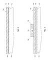
- FIGS. 2-13 illustrate a process for forming a mirror image pair of n-channel gallium nitride transistors, according to one embodiment of the present description.
- a stacked substrate 130 may be formed comprising the charge inducing layer 108 formed on the gallium nitride layer 102 .
- the charge inducing layer 108 may comprise the polarization layer 114 formed on the crystal transition layer 116 , wherein the crystal transition layer 116 abuts the gallium nitride layer 102 .
- a hardmask 132 such as silicon nitride, silicon oxide, and the like, may be patterned by any known technique, such as photolithography, on the polarization layer 114 .
- the hardmask 132 may define a region for a shared drain for the mirror image pair of n-channel gallium nitride transistors to be formed.
- a first spacer material 142 may be deposited over the hardmask 132 and the gallium nitride layer 102 , as shown in FIG. 5 , the first spacer material 142 (see FIG. 4 ) may be etched to expose a top surface 134 of the hardmask 132 and expose portions of the polarization layer 114 , whereby first spacers 144 are formed on opposing sides 136 of the hardmask 132 .
- a width W 1 of the first spacers 144 may define the gate-to-drain length L GD (see FIG. 1 ) for each one of the pair of n-channel gallium nitride transistors to be formed.
- a second spacer material 152 may be deposited over the hardmask top surface 134 , the first spacers 144 , and the polarization layer 114 .
- the second spacer material 152 (see FIG. 6 ) may be etched to expose the hardmask top surface 134 , a top surface 146 of the first spacers 144 , and expose portions of the polarization layer 114 , whereby second spacers 154 are formed on opposing hardmask sides 136 abutting the first spacers 144 .
- a width W 2 of the second spacers 154 may define the channel or gate length L G (see FIG. 1 ) for each one of the pair of n-channel gallium nitride transistors.
- a third spacer material 162 may be deposited over the hardmask top surface 134 , the first spacers 144 , the second spacers 154 , and the polarization layer 114 .
- the third spacer material 162 (see FIG. 8 ) may be etched to expose the hardmask top surface 134 , the first spacer top surfaces 146 , a top surface 156 of the second spacers 154 , and portions of the polarization layer 114 , whereby third spacers 164 are formed on opposing hardmask sides 136 abutting the second spacers 154 .
- a width W 3 of the third spacers 164 may define the gate-to-source length L GS (see FIG. 1 ) for each one of the pair of n-channel gallium nitride transistors to be formed.
- the hardmask 132 may be removed and, using the first spacers 144 , the second spacers 154 , and the third spacers 164 as etch masks, recesses 172 may be formed to extend through the charge inducing layer 108 (e.g. the polarization layer 114 and the crystal transition layer 116 ) and into the gallium nitride layer 102 , by any known technique, such as etching.
- the recesses 172 may be formed with a plasma etch in a chlorine based chemistry.
- the source structures 104 and the shared drain structure 106 may be formed by epitaxial regrowth from the gallium nitride layer 102 .
- the regrowth process may comprise epitaxial crystal growth techniques, such as metal organic chemical vapor deposition (MOCVD) or molecular beam epitaxy (MBE).
- MOCVD metal organic chemical vapor deposition
- MBE molecular beam epitaxy
- the second spacers 154 may be removed, as well as a portion of the polarization layer 114 to form gate recesses 174 in the polarization layer 114 , which, as previously discussed, disrupts the 2D electron gas 112 , such that it does not extend through a gate length L g (previously labeled width W 2 ) to achieve enhancement mode operation.
- the gate dielectric layer 118 may be formed on the polarization layer 114 within the recesses 174 (see FIG. 12 ) and the gate electrodes 122 may be formed on the gate dielectric layer 118 such that the gate dielectric layer 118 electrically isolates the gate electrode 122 from the polarization layer 114 to from the n-channel gallium nitride transistors 100 1 and 100 2 .
- source contacts 124 and drain contacts 126 may be formed on the source structures 104 and the drain structure 106 , respectively.
- an interconnection structure (not shown) would be formed over the n-channel gallium nitride transistors 100 1 and 100 2 to appropriately connect the gate electrodes 122 , the source contacts 124 , and the drain contacts 126 with external components (not shown). However, for the sake of brevity and conciseness, the interconnection structure is not shown.
- FIG. 14 is a flow chart of a process 200 of fabricating an n-channel gallium nitride transistor according to an embodiment of the present description.
- a gallium nitride layer may be formed.
- a charge inducing layer may be formed on the gallium nitride layer to form a 2D electron gas within the gallium nitride layer, as set forth in block 204 .
- a source structure and a drain structure may be formed in the gallium nitride layer.
- a recess may be formed within the polarization layer between the source structure and the drain structure, wherein a thickness of a portion of the polarization layer which is between the recess and the gallium nitride layer is less than about 1 nm, as set in block 208 .
- a gate dielectric may be formed in the recess.
- a gate electrode may be formed adjacent the gate dielectric, as set forth in block 212 .
- FIG. 15 illustrates a wireless power/charging device 300 , according to an embodiment of the present description.
- the wireless power/charging device 300 may include a transmission module 310 and a receiving module 330 .
- the transmission module 310 may comprise a power unit 312 (such as an AC to DC converter), a transmitter 314 , a coil assembly 316 , a controller 318 , and a communication unit 322 (such as for radio frequency communication illustrated by arrows 324 ).
- the receiving module 330 such as components within a mobile device or a device which plugs into a mobile device, may comprise a load unit 332 which includes a voltage regulator and a battery, a rectifier 334 , a coil assembly 336 , a controller 338 , and a communication unit 342 (such as for radio frequency communication illustrated by arrows 344 ).
- a load unit 332 which includes a voltage regulator and a battery
- a rectifier 334 a rectifier 334
- a coil assembly 336 such as for radio frequency communication illustrated by arrows 344
- the specific interconnections and component operations of such a wireless power/charge device 300 are well known in the art and for the sake of brevity and conciseness will not be discussed herein.
- high voltage n-channel gallium nitride transistors 100 may be utilized in place of silicon power MOSFETs, as n-channel gallium nitride transistors have on-state resistances that are about three times better at the given breakdown voltage of 40V
- the n-channel gallium transistor 100 may be utilized in the transmitter 314 of the transmission module 310 .
- the transmitter 314 i.e. full-bridge inverter
- the transmitter 314 may have four n-channel gallium nitride transistors T 1 , T 2 , T 3 , and T 4 .
- the n-channel gallium nitride transistors T 1 , T 2 , T 3 , and T 4 may enable at least a 10% higher DC-to-AC conversion efficiency than silicon transistors.
- the use of the n-channel gallium nitride transistors T 1 , T 2 , T 3 , and T 4 may enable wireless power transmission over the air at 10 MHz or higher, which is over 100 times higher frequency than with comparable silicon transistors, and enabling distance transmission up to 2 meters (illustrated with an arrow 350 ), which is over 25 times longer than with comparable silicon transistors.
- the form factor of the transmission module coil assembly 316 and the receiving module coil assembly 336 may be as much as ten times thinner.
- utilizing the n-channel gallium nitride transistors 100 (see FIG. 1 ) in the voltage regulator of the receiving module load unit 332 may result in as much as a 100 times smaller form factor for the receiving module 330 and up to 7% higher efficiency than voltage regulators having silicon transistors. It is anticipated that an overall wireless power transmit efficiency improvement of 14% through the utilization n-channel gallium nitride transistors 100 (see FIG. 1 ) of the present description in the transmission module 310 and the receiving module 330 .
- the circuit design of a voltage regulator is well known in the art, and thus, for the sake of brevity and conciseness, is not illustrated with specificity.
- Example 1 is an re-channel gallium nitride transistor, comprising a gallium nitride layer; a source structure and a drain structure formed in the gallium nitride layer; a charge inducing layer comprising a polarization layer extending between the structure and the drain structure; a 2D electron gas within the gallium nitride layer; and a gate electrode extending at least partially into the polarization layer, wherein a thickness of a portion of the polarization layer which is between the gate electrode and the gallium nitride layer is less than about 1 nm.
- Example 2 the subject matter of Example 1 can optionally include a gate dielectric disposed between the gate electrode and the polarization layer.
- Example 3 the subject matter of either of Examples 1 or 2 can optionally include a portion of the polarization layer which is not between the gate electrode and the gallium nitride layer being between about 5 nm and 10 nm.
- Example 4 the subject matter of any of Examples 1 to 3 can optionally include the polarization layer being selected from the group consisting of aluminum gallium nitride, aluminum indium nitride, and indium gallium nitride.
- Example 5 the subject matter of any of Examples 1 to 4 can optionally include a crystal transition layer disposed between the gallium nitride layer and the polarization layer.
- Example 6 the subject matter of Example 5 can optionally include the crystal transition layer being selected from the group consisting of indium nitride and aluminum nitride.
- Example 7 the subject matter of any of Examples 1 to 6 can optionally include a gate-to-drain length between about 120 nm to about 400 nm and a gate-to-source length between about 5 nm to about 400 nm.
- Example 8 the subject matter of Example 7 can optionally include the gate-to drain length being greater than the gate-to-source length.
- Example 9 is a method of forming an n-channel gallium nitride transistor, comprising forming a gallium nitride layer; forming a charge inducing layer comprising a polarization layer on the gallium nitride layer to form a 2D electron gas within the gallium nitride layer; forming a source structure and a drain structure formed in the gallium nitride layer; forming a recess within the polarization layer between the source structure and the drain structure, wherein a thickness of a portion of the polarization layer which is between the recess and the gallium nitride layer is less than about 1 nm; forming asymmetrical dielectric spacers of different widths; forming a gate dielectric within the recess; and forming a gate electrode adjacent the gate dielectric.
- Example 10 the subject matter of Example 9 can optionally include forming the charge inducing layer comprising the polarization layer on the gallium nitride layer comprises forming the charge inducing layer comprising the polarization layer having a thickness of between about 5 nm and 10 nm.
- Example 11 the subject matter of either of Examples 9 or 10 can optionally include forming the polarization layer selected from the group consisting of aluminum gallium nitride, aluminum indium nitride, and indium gallium nitride.
- Example 12 the subject matter of any of Examples 9 to 11 can optionally include forming a crystal transition layer between the gallium nitride layer and the polarization layer.
- Example 13 the subject matter of Example 12 can optionally include forming the crystal transition layer from a material selected from the group consisting of indium nitride and aluminum nitride.
- Example 14 the subject matter of any of Examples 9 to 13 can optionally include forming a gate-to-drain length between about 120 nm to about 400 nm and forming a gate-to-source length between about 5 nm to about 400 nm.
- Example 15 the subject matter of Example 14 can optionally include the gate-to-drain length being greater than the gate-to-source length.
- Example 16 is a wireless power/charging device transmission module, comprising a coil assembly; and a transmitter, wherein the transmitter includes at least one n-channel gallium nitride transistor, comprising: a gallium nitride layer; a source structure and a drain structure formed in the gallium nitride layer; a charge inducing layer comprising a polarization layer extending between the structure and the drain structure; a 2D electron gas within the gallium nitride layer; and a gate electrode extending at least partially into the polarization layer.
- the transmitter includes at least one n-channel gallium nitride transistor, comprising: a gallium nitride layer; a source structure and a drain structure formed in the gallium nitride layer; a charge inducing layer comprising a polarization layer extending between the structure and the drain structure; a 2D electron gas within the gallium nitride layer; and a gate electrode extending at least partially into the polarization
- Example 17 the subject matter of Example 16 can optionally include a thickness of a portion of the polarization layer which is between the gate electrode and the gallium nitride layer being less than about 1 nm.
- Example 18 the subject matter of either of Example 16 or 17 can optionally include a gate dielectric disposed between the gate electrode and the polarization layer.
- Example 19 the subject matter of any of Examples 16 to 18 can optionally include a portion of the polarization layer which is between the gate electrode and the gallium nitride layer being between about 5 nm and 10 nm.
- Example 20 the subject matter of any of Example 16 to 19 can optionally include a crystal transition layer disposed between the gallium nitride layer and the polarization layer.
- Example 21 is a wireless power/charging device receiving module, comprising a coil assembly; a rectifier; and a load unit including a voltage regulator and a battery, wherein the voltage regulator includes at least one n-channel gallium nitride transistor, comprising: a gallium nitride layer; a source structure and a drain structure formed in the gallium nitride layer; a charge inducing layer comprising a polarization layer extending between the structure and the drain structure; a 2D electron gas within the gallium nitride layer; and a gate electrode extending at least partially into the polarization layer.
- the voltage regulator includes at least one n-channel gallium nitride transistor, comprising: a gallium nitride layer; a source structure and a drain structure formed in the gallium nitride layer; a charge inducing layer comprising a polarization layer extending between the structure and the drain structure; a 2D electron gas within the gallium nitride
- Example 22 the subject matter of Example 21 can optionally include a thickness of a portion of the polarization layer which is between the gate electrode and the gallium nitride layer being less than about 1 nm.
- Example 23 the subject matter of either of Example 21 or 22 can optionally include a gate dielectric disposed between the gate electrode and the polarization layer.
- Example 24 the subject matter of any of Examples 21 to 23 can optionally include a portion of the polarization layer which is between the gate electrode and the gallium nitride layer being between about 5 nm and 10 nm.
- Example 25 the subject matter of any of Example 21 to 24 can optionally include a crystal transition layer disposed between the gallium nitride layer and the polarization layer.
Abstract
The present description relates to n-channel gallium nitride transistors which include a recessed gate electrode, wherein the polarization layer between the gate electrode and the gallium nitride layer is less than about 1 nm. In additional embodiments, the n-channel gallium nitride transistors may have an asymmetric configuration, wherein a gate-to drain length is greater than a gate-to-source length. In further embodiment, the n-channel gallium nitride transistors may be utilized in wireless power/charging devices for improved efficiencies, longer transmission distances, and smaller form factors, when compared with wireless power/charging devices using silicon-based transistors.
Description
The present application is a national stage entry of PCT Patent Application No. PCT/US2014/071163, filed on Dec. 18, 2014, entitled “N-CHANNEL GALLIUM NITRIDE TRANSISTORS”, which is hereby incorporated herein by reference in its entirety and for all purposes.
Embodiments of the present description generally relate to the field of microelectronic devices, and, more particularly, to forming n-channel gallium nitride transistors and the use thereof in wireless power/charging devices.
The microelectronics industry is continually striving to produce ever faster and smaller microelectronic packages for use in various electronic products, including, but not limited to, computer server products and portable products, such as laptop/netbook computers, electronic tablets, smart phones, digital cameras, and the like. One route to achieve these goals is the fabrication of System-on-Chip (SoC) devices, wherein all of the components of an electronic system are fabricated on a single chip. In such SoC devices, power management integrated circuits (PMIC) and radio frequency integrated circuits (RFIC) are critical functional blocks, and are as important as logic and memory integrated circuits in determining the power efficiency and the form factor of such SoC devices. Moreover, there is a growing need to power and/or charge mobile devices wirelessly. Solutions for wireless power/charging devices employing silicon power Metal-on-Semiconductor Field Effect Transistors (MOSFET) have emerged in the marketplace. However, these silicon power MOSFETs require considerable power and dissipates substantial power, due to their high on-state resistance and large capacitance, which could otherwise be usefully transmitted wirelessly to power and/or charge mobile devices. Therefore, there is an ongoing effort to scaled down and/or improve the efficiency of such wireless power/charging devices.
The subject matter of the present disclosure is particularly pointed out and distinctly claimed in the concluding portion of the specification. The foregoing and other features of the present disclosure will become more fully apparent from the following description and appended claims, taken in conjunction with the accompanying drawings. It is understood that the accompanying drawings depict only several embodiments in accordance with the present disclosure and are, therefore, not to be considered limiting of its scope. The disclosure will be described with additional specificity and detail through use of the accompanying drawings, such that the advantages of the present disclosure can be more readily ascertained, in which:
In the following detailed description, reference is made to the accompanying drawings that show, by way of illustration, specific embodiments in which the claimed subject matter may be practiced. These embodiments are described in sufficient detail to enable those skilled in the art to practice the subject matter. It is to be understood that the various embodiments, although different, are not necessarily mutually exclusive. For example, a particular feature, structure, or characteristic described herein, in connection with one embodiment, may be implemented within other embodiments without departing from the spirit and scope of the claimed subject matter. References within this specification to “one embodiment” or “an embodiment” mean that a particular feature, structure, or characteristic described in connection with the embodiment is included in at least one implementation encompassed within the present description. Therefore, the use of the phrase “one embodiment” or “in an embodiment” does not necessarily refer to the same embodiment. In addition, it is to be understood that the location or arrangement of individual elements within each disclosed embodiment may be modified without departing from the spirit and scope of the claimed subject matter. The following detailed description is, therefore, not to be taken in a limiting sense, and the scope of the subject matter is defined only by the appended claims, appropriately interpreted, along with the full range of equivalents to which the appended claims are entitled. In the drawings, like numerals refer to the same or similar elements or functionality throughout the several views, and that elements depicted therein are not necessarily to scale with one another, rather individual elements may be enlarged or reduced in order to more easily comprehend the elements in the context of the present description.
The terms “over”, “to”, “between” and “on” as used herein may refer to a relative position of one layer with respect to other layers. One layer “over” or “on” another layer or bonded “to” another layer may be directly in contact with the other layer or may have one or more intervening layers. One layer “between” layers may be directly in contact with the layers or may have one or more intervening layers.
Embodiments of the present description relate to n-channel gallium nitride transistors which include a recessed gate electrode wherein the polarization layer between the gate electrode and the gallium nitride layer is less than about 1 nm. In additional embodiments, the n-channel gallium nitride transistors may have an asymmetric configuration, wherein a gate-to drain length is greater than a gate-to-source length. In further embodiment, the n-channel gallium nitride transistors may be utilized in wireless power/charging devices for improved efficiencies, longer transmission distances, and smaller form factors when compared with wireless power/charging devices using silicon-based transistors.
In one embodiment, the n-channel gallium nitride transistor 100 is an enhancement mode transistor. Thus, as illustrated in FIG. 1 , a portion of the polarization layer 114 may be removed proximate forming a recess 120 in a desired location for a gate electrode 122 to disrupt the 2D electron gas 112, such that it does not extend through a gate length Lg of the n-channel gallium nitride transistor 100 to achieve enhancement mode operation.
As shown, a gate dielectric layer 118 may be formed over the polarization layer 114 and the gate electrode 122 may be formed on the gate dielectric layer 118, such that the gate dielectric layer 118 electrically isolates the gate electrode 122 from the polarization layer 114. Furthermore, source contacts 124 and drain contacts 126 may formed on the source structure 104 and the drain structure 106, respectively, and may be utilized to form electrical connections with external components (not shown) through the formation of interconnection structure (not shown), as will be understood to those skilled in the art.
As further illustrated in FIG. 1 , the n-channel gallium nitride transistor 100 may include a gate-to-drain length LGD (i.e. from the gate to the drain structure 106) and a gate-to-source length LGS (i.e. from the gate to the source structure 104). In one embodiment, the gate-to-drain length LGD may range from about 120 nm to about 400 nm. In other embodiment, the gate-to-source length LGS may range from about 5 nm to about 400 nm. In still another embodiment, the gate length LG may range from about 20 nm to about 500 nm. In one embodiment, the n-channel gallium nitride transistor 100 may have an asymmetric structure with a gate-to-drain length LGD (i.e. from the gate to the drain structure 106) larger than a gate-to-source length LGS (i.e. from the gate to the source structure 104), which will minimize resistance between across the gate-to-source length LGS, as will be understood to those skilled in the art.
The polarization layer 114 may include, but is not limited to aluminum gallium nitride, aluminum indium nitride, and indium gallium nitride. In one embodiment, the polarization layer 114 is Al0.83In0.17N. In one embodiment, the polarization layer 114 may be have a thickness T1 of between about 5 nm and 10 nm over the gate-to-drain length LGD area and over the gate-to-source length LGS area, which may achieve low on-state resistance. In a further embodiment, the polarization layer 114 may have a thickness T2 of less than about 1 nm over the gate length LG area, which may achieve enhancement mode operation. In another embodiment, the crystal transition layer 116 may include, but is not limited to, indium nitride and aluminum nitride, and may have a thickness T3 of less than about 1 nm.
The gate dielectric layer 118 may be formed from any well-known gate dielectric material, including but not limited to silicon dioxide (SiO2), silicon oxynitride (SiOxNy), silicon nitride (Si3N4), and high-k dielectric materials such as hafnium oxide, hafnium silicon oxide, lanthanum oxide, lanthanum aluminum oxide, zirconium oxide, zirconium silicon oxide, tantalum oxide, tantalum silicon oxide, titanium oxide, barium strontium titanium oxide, barium titanium oxide, strontium titanium oxide, yttrium oxide, aluminum oxide, lead scandium tantalum oxide, and lead zinc niobate. It is noted that a high-K gate dielectric layer 118 may be advantageous to achieve low gate leakages. The gate dielectric layer 118 can be formed by well-known techniques, such as chemical vapor deposition (“CVD”), physical vapor deposition (“PVD”), atomic layer deposition (“ALD”).
The gate electrode 122 can be formed of any suitable gate electrode material. In an embodiment of the present disclosure, the gate electrode 122 may be formed from materials that include, but are not limited to, polysilicon, tungsten, ruthenium, palladium, platinum, cobalt, nickel, hafnium, zirconium, titanium, tantalum, aluminum, titanium carbide, zirconium carbide, tantalum carbide, hafnium carbide, aluminum carbide, other metal carbides, metal nitrides, and metal oxides. The gate electrode 122 can be formed by well-known techniques, such as by blanket depositing a gate electrode material and then patterning the gate electrode material with well-known photolithography and etching techniques, as will be understood to those skilled in the art.
Gallium nitride has a relatively wide bandgap (e.g. about 3.4 eV), when compared to the bandgap of silicon (about 1.1 eV). Therefore, the n-channel gallium nitride transistor 100 may withstand large electric fields, such as applied voltages, drain voltage, and the like, before suffering breakdown, when compared to a silicon based transistor of similar dimensions. This also enables n-channel gallium nitride transistors 100 to be scaled to even smaller physical dimensions while operating at the same supply voltage; thus, enabling small on-state resistance and smaller capacitance, which may result in reduced power dissipation and hence higher circuit efficiencies. Furthermore, as will be understood to those skilled in the art, the n-channel gallium nitride transistor 100 employs the 2D electron gas 112 as its electron transport channel for the operation thereof. The 2D electron gas 112 is formed at the abrupt hetero-interface formed by the deposition of the charge inducing layer 108 on the gallium nitride layer 102 through spontaneous and piezoelectric polarization, as will be understood to those skilled in the art. Very high charge densities up to about 2E13 per cm2 can be formed by such a mechanism, without the use of impurity dopants, which allows for high electron mobility, e.g. greater than about 1000 cm2/Vs (low sheet resistance at LGD and LGS regions). As will be understood to those skilled in the art, the n-channel gallium nitride transistor 100 may enable low parasitic leakages due to absence of band-to-band tunneling, low gate induced drain leakage (GIDL), and low generation of electron-hole pairs from impact ionization from hot electrons.
As shown in FIG. 3 , a hardmask 132, such as silicon nitride, silicon oxide, and the like, may be patterned by any known technique, such as photolithography, on the polarization layer 114. The hardmask 132 may define a region for a shared drain for the mirror image pair of n-channel gallium nitride transistors to be formed.
As shown in FIG. 4 , a first spacer material 142 may be deposited over the hardmask 132 and the gallium nitride layer 102, as shown in FIG. 5 , the first spacer material 142 (see FIG. 4 ) may be etched to expose a top surface 134 of the hardmask 132 and expose portions of the polarization layer 114, whereby first spacers 144 are formed on opposing sides 136 of the hardmask 132. A width W1 of the first spacers 144 may define the gate-to-drain length LGD (see FIG. 1 ) for each one of the pair of n-channel gallium nitride transistors to be formed.
As shown in FIG. 6 , a second spacer material 152 may be deposited over the hardmask top surface 134, the first spacers 144, and the polarization layer 114. As shown in FIG. 7 , the second spacer material 152 (see FIG. 6 ) may be etched to expose the hardmask top surface 134, a top surface 146 of the first spacers 144, and expose portions of the polarization layer 114, whereby second spacers 154 are formed on opposing hardmask sides 136 abutting the first spacers 144. A width W2 of the second spacers 154 may define the channel or gate length LG (see FIG. 1 ) for each one of the pair of n-channel gallium nitride transistors.
As shown in FIG. 8 , a third spacer material 162 may be deposited over the hardmask top surface 134, the first spacers 144, the second spacers 154, and the polarization layer 114. As shown in FIG. 9 , the third spacer material 162 (see FIG. 8 ) may be etched to expose the hardmask top surface 134, the first spacer top surfaces 146, a top surface 156 of the second spacers 154, and portions of the polarization layer 114, whereby third spacers 164 are formed on opposing hardmask sides 136 abutting the second spacers 154. A width W3 of the third spacers 164 may define the gate-to-source length LGS (see FIG. 1 ) for each one of the pair of n-channel gallium nitride transistors to be formed.
As shown in FIG. 10 , the hardmask 132 (see FIG. 9 ) may be removed and, using the first spacers 144, the second spacers 154, and the third spacers 164 as etch masks, recesses 172 may be formed to extend through the charge inducing layer 108 (e.g. the polarization layer 114 and the crystal transition layer 116) and into the gallium nitride layer 102, by any known technique, such as etching. In one embodiment, the recesses 172 may be formed with a plasma etch in a chlorine based chemistry.
As shown in FIG. 11 , the source structures 104 and the shared drain structure 106, such as N+ indium gallium nitride, N+ gallium nitride, N+ indium nitride, and any graded combination thereof, may be formed by epitaxial regrowth from the gallium nitride layer 102. In one embodiment, the regrowth process may comprise epitaxial crystal growth techniques, such as metal organic chemical vapor deposition (MOCVD) or molecular beam epitaxy (MBE).
As shown in FIG. 12 , the second spacers 154 may be removed, as well as a portion of the polarization layer 114 to form gate recesses 174 in the polarization layer 114, which, as previously discussed, disrupts the 2D electron gas 112, such that it does not extend through a gate length Lg (previously labeled width W2) to achieve enhancement mode operation.
As shown in FIG. 13 , the gate dielectric layer 118 may be formed on the polarization layer 114 within the recesses 174 (see FIG. 12 ) and the gate electrodes 122 may be formed on the gate dielectric layer 118 such that the gate dielectric layer 118 electrically isolates the gate electrode 122 from the polarization layer 114 to from the n-channel gallium nitride transistors 100 1 and 100 2. Furthermore, source contacts 124 and drain contacts 126 may be formed on the source structures 104 and the drain structure 106, respectively. As will be understood to those, skilled in the art an interconnection structure (not shown) would be formed over the n-channel gallium nitride transistors 100 1 and 100 2 to appropriately connect the gate electrodes 122, the source contacts 124, and the drain contacts 126 with external components (not shown). However, for the sake of brevity and conciseness, the interconnection structure is not shown.
In one embodiment of the present description, the n-channel gallium transistor 100 (see FIG. 1 ) may be utilized in the transmitter 314 of the transmission module 310. As shown in FIG. 16 , the transmitter 314 (i.e. full-bridge inverter) may have four n-channel gallium nitride transistors T1, T2, T3, and T4. Such a configuration, the n-channel gallium nitride transistors T1, T2, T3, and T4 may enable at least a 10% higher DC-to-AC conversion efficiency than silicon transistors. Furthermore, the use of the n-channel gallium nitride transistors T1, T2, T3, and T4 may enable wireless power transmission over the air at 10 MHz or higher, which is over 100 times higher frequency than with comparable silicon transistors, and enabling distance transmission up to 2 meters (illustrated with an arrow 350), which is over 25 times longer than with comparable silicon transistors. Moreover, with the higher wireless power transmission frequencies, the form factor of the transmission module coil assembly 316 and the receiving module coil assembly 336 may be as much as ten times thinner.
In a further embodiment, utilizing the n-channel gallium nitride transistors 100 (see FIG. 1 ) in the voltage regulator of the receiving module load unit 332 may result in as much as a 100 times smaller form factor for the receiving module 330 and up to 7% higher efficiency than voltage regulators having silicon transistors. It is anticipated that an overall wireless power transmit efficiency improvement of 14% through the utilization n-channel gallium nitride transistors 100 (see FIG. 1 ) of the present description in the transmission module 310 and the receiving module 330. The circuit design of a voltage regulator is well known in the art, and thus, for the sake of brevity and conciseness, is not illustrated with specificity.
It is understood that the subject matter of the present description is not necessarily limited to specific applications illustrated in FIGS. 1-16 . The subject matter may be applied to other microelectronic device and assembly applications, as well as any other appropriate transistor applications, as will be understood to those skilled in the art.
The following examples pertain to further embodiments, wherein Example 1 is an re-channel gallium nitride transistor, comprising a gallium nitride layer; a source structure and a drain structure formed in the gallium nitride layer; a charge inducing layer comprising a polarization layer extending between the structure and the drain structure; a 2D electron gas within the gallium nitride layer; and a gate electrode extending at least partially into the polarization layer, wherein a thickness of a portion of the polarization layer which is between the gate electrode and the gallium nitride layer is less than about 1 nm.
In Example 2, the subject matter of Example 1 can optionally include a gate dielectric disposed between the gate electrode and the polarization layer.
In Example 3, the subject matter of either of Examples 1 or 2 can optionally include a portion of the polarization layer which is not between the gate electrode and the gallium nitride layer being between about 5 nm and 10 nm.
In Example 4, the subject matter of any of Examples 1 to 3 can optionally include the polarization layer being selected from the group consisting of aluminum gallium nitride, aluminum indium nitride, and indium gallium nitride.
In Example 5, the subject matter of any of Examples 1 to 4 can optionally include a crystal transition layer disposed between the gallium nitride layer and the polarization layer.
In Example 6, the subject matter of Example 5 can optionally include the crystal transition layer being selected from the group consisting of indium nitride and aluminum nitride.
In Example 7, the subject matter of any of Examples 1 to 6 can optionally include a gate-to-drain length between about 120 nm to about 400 nm and a gate-to-source length between about 5 nm to about 400 nm.
In Example 8, the subject matter of Example 7 can optionally include the gate-to drain length being greater than the gate-to-source length.
The following examples pertain to further embodiments, wherein Example 9 is a method of forming an n-channel gallium nitride transistor, comprising forming a gallium nitride layer; forming a charge inducing layer comprising a polarization layer on the gallium nitride layer to form a 2D electron gas within the gallium nitride layer; forming a source structure and a drain structure formed in the gallium nitride layer; forming a recess within the polarization layer between the source structure and the drain structure, wherein a thickness of a portion of the polarization layer which is between the recess and the gallium nitride layer is less than about 1 nm; forming asymmetrical dielectric spacers of different widths; forming a gate dielectric within the recess; and forming a gate electrode adjacent the gate dielectric.
In Example 10, the subject matter of Example 9 can optionally include forming the charge inducing layer comprising the polarization layer on the gallium nitride layer comprises forming the charge inducing layer comprising the polarization layer having a thickness of between about 5 nm and 10 nm.
In Example 11, the subject matter of either of Examples 9 or 10 can optionally include forming the polarization layer selected from the group consisting of aluminum gallium nitride, aluminum indium nitride, and indium gallium nitride.
In Example 12, the subject matter of any of Examples 9 to 11 can optionally include forming a crystal transition layer between the gallium nitride layer and the polarization layer.
In Example 13, the subject matter of Example 12 can optionally include forming the crystal transition layer from a material selected from the group consisting of indium nitride and aluminum nitride.
In Example 14, the subject matter of any of Examples 9 to 13 can optionally include forming a gate-to-drain length between about 120 nm to about 400 nm and forming a gate-to-source length between about 5 nm to about 400 nm.
In Example 15, the subject matter of Example 14 can optionally include the gate-to-drain length being greater than the gate-to-source length.
The following examples pertain to further embodiments, wherein Example 16 is a wireless power/charging device transmission module, comprising a coil assembly; and a transmitter, wherein the transmitter includes at least one n-channel gallium nitride transistor, comprising: a gallium nitride layer; a source structure and a drain structure formed in the gallium nitride layer; a charge inducing layer comprising a polarization layer extending between the structure and the drain structure; a 2D electron gas within the gallium nitride layer; and a gate electrode extending at least partially into the polarization layer.
In Example 17, the subject matter of Example 16 can optionally include a thickness of a portion of the polarization layer which is between the gate electrode and the gallium nitride layer being less than about 1 nm.
In Example 18, the subject matter of either of Example 16 or 17 can optionally include a gate dielectric disposed between the gate electrode and the polarization layer.
In Example 19, the subject matter of any of Examples 16 to 18 can optionally include a portion of the polarization layer which is between the gate electrode and the gallium nitride layer being between about 5 nm and 10 nm.
In Example 20, the subject matter of any of Example 16 to 19 can optionally include a crystal transition layer disposed between the gallium nitride layer and the polarization layer.
The following examples pertain to further embodiments, wherein Example 21 is a wireless power/charging device receiving module, comprising a coil assembly; a rectifier; and a load unit including a voltage regulator and a battery, wherein the voltage regulator includes at least one n-channel gallium nitride transistor, comprising: a gallium nitride layer; a source structure and a drain structure formed in the gallium nitride layer; a charge inducing layer comprising a polarization layer extending between the structure and the drain structure; a 2D electron gas within the gallium nitride layer; and a gate electrode extending at least partially into the polarization layer.
In Example 22, the subject matter of Example 21 can optionally include a thickness of a portion of the polarization layer which is between the gate electrode and the gallium nitride layer being less than about 1 nm.
In Example 23, the subject matter of either of Example 21 or 22 can optionally include a gate dielectric disposed between the gate electrode and the polarization layer.
In Example 24, the subject matter of any of Examples 21 to 23 can optionally include a portion of the polarization layer which is between the gate electrode and the gallium nitride layer being between about 5 nm and 10 nm.
In Example 25, the subject matter of any of Example 21 to 24 can optionally include a crystal transition layer disposed between the gallium nitride layer and the polarization layer.
Having thus described in detail embodiments of the present description, it is understood that the present description defined by the appended claims is not to be limited by particular details set forth in the above description, as many apparent variations thereof are possible without departing from the spirit or scope thereof.
Claims (25)
1. An n-channel gallium nitride transistor, comprising:
a gallium nitride layer;
a source structure and a drain structure formed in the gallium nitride layer;
a charge inducing layer comprising a polarization layer extending between the source structure and the drain structure;
a 2D electron gas within the gallium nitride layer; and
a gate electrode extending at least partially into the polarization layer, wherein a thickness of a portion of the polarization layer which is between the gate electrode and the gallium nitride layer is less than about 1 nm.
2. The n-channel gallium nitride transistor of claim 1 , further comprising a gate dielectric disposed between the gate electrode and the polarization layer.
3. The n-channel gallium nitride transistor of claim 1 , further comprising a portion of the polarization layer which is not between the gate electrode and the gallium nitride layer is between about 5 nm and 10 nm.
4. The n-channel gallium nitride transistor of claim 1 , wherein the polarization layer is selected from the group consisting of aluminum gallium nitride, aluminum indium nitride, and indium gallium nitride.
5. The n-channel gallium nitride transistor of claim 1 , further including a crystal transition layer disposed between the gallium nitride layer and the polarization layer.
6. The n-channel gallium nitride transistor of claim 5 , wherein the crystal transition layer is selected from the group consisting of indium nitride and aluminum nitride.
7. The n-channel gallium nitride transistor of claim 1 , further including a gate-to-drain length between about 120 nm to about 400 nm and a gate-to-source length between about 5 nm to about 400 nm.
8. The n-channel gallium nitride transistor of claim 7 , wherein the gate-to drain length is greater than the gate-to-source length.
9. A method of forming an n-channel gallium nitride transistor, comprising:
forming a gallium nitride layer;
forming a charge inducing layer comprising a polarization layer on the gallium nitride layer to form a 2D electron gas within the gallium nitride layer;
forming a source structure and a drain structure formed in the gallium nitride layer;
forming a recess within the polarization layer between the source structure and the drain structure, wherein a thickness of a portion of the polarization layer which is between the recess and the gallium nitride layer is less than about 1 nm;
forming asymmetrical dielectric spacers of different widths;
forming a gate dielectric within the recess; and
forming a gate electrode adjacent the gate dielectric.
10. The method of claim 9 , wherein forming the charge inducing layer comprising the polarization layer on the gallium nitride layer comprises forming the charge inducing layer comprising the polarization layer having a thickness of between about 5 nm and 10 nm.
11. The method of claim 9 , wherein forming the charge inducing layer comprises forming the polarization layer selected from the group consisting of aluminum gallium nitride, aluminum indium nitride, and indium gallium nitride.
12. The method of claim 9 , further including forming a crystal transition layer between the gallium nitride layer and the polarization layer.
13. The method of claim 12 , wherein forming the crystal transition layer comprises forming the crystal transition layer from a material selected from the group consisting of indium nitride and aluminum nitride.
14. The method of claim 9 , further including forming a gate-to-drain length between about 120 nm to about 400 nm and forming a gate-to-source length between about 5 nm to about 400 nm.
15. The method of claim 14 , wherein the gate-to-drain length is greater than the gate-to-source length.
16. A wireless power/charging device transmission module, comprising:
a coil assembly; and
a transmitter, wherein the transmitter includes at least one n-channel gallium nitride transistor, comprising:
a gallium nitride layer;
a source structure and a drain structure formed in the gallium nitride layer;
a charge inducing layer comprising a polarization layer extending between the source structure and the drain structure;
a 2D electron gas within the gallium nitride layer; and
a gate electrode extending at least partially into the polarization layer.
17. The wireless power/charging device transmission module of claim 16 , wherein a thickness of a portion of the polarization layer which is between the gate electrode and the gallium nitride layer is less than about 1 nm.
18. The wireless power/charging device transmission module of claim 16 , further comprising a gate dielectric disposed between the gate electrode and the polarization layer.
19. The wireless power/charging device transmission module of claim 16 , further comprising a portion of the polarization layer which is between the gate electrode and the gallium nitride layer is between about 5 nm and 10 nm.
20. The wireless power/charging device transmission module of claim 16 , further including a crystal transition layer disposed between the gallium nitride layer and the polarization layer.
21. A wireless power/charging device receiving module, comprising:
a coil assembly;
a rectifier; and
a load unit including a voltage regulator and a battery, wherein the voltage regulator includes at least one n-channel gallium nitride transistor, comprising:
a gallium nitride layer;
a source structure and a drain structure formed in the gallium nitride layer;
a charge inducing layer comprising a polarization layer extending between the source structure and the drain structure;
a 2D electron gas within the gallium nitride layer; and
a gate electrode extending at least partially into the polarization layer.
22. The wireless power/charging device receiving module of claim 21 , wherein a thickness of a portion of the polarization layer which is between the gate electrode and the gallium nitride layer is less than about 1 nm.
23. The wireless power/charging device receiving module of claim 21 , further comprising a gate dielectric disposed between the gate electrode and the polarization layer.
24. The wireless power/charging device receiving module of claim 21 , further comprising a portion of the polarization layer which is between the gate electrode and the gallium nitride layer is between about 5 nm and 10 nm.
25. The wireless power/charging device receiving module of claim 21 , further including a crystal transition layer disposed between the gallium nitride layer and the polarization layer.
Applications Claiming Priority (1)
| Application Number | Priority Date | Filing Date | Title |
|---|---|---|---|
| PCT/US2014/071163 WO2016099509A1 (en) | 2014-12-18 | 2014-12-18 | N-channel gallium nitride transistors |
Related Parent Applications (1)
| Application Number | Title | Priority Date | Filing Date |
|---|---|---|---|
| PCT/US2014/071163 A-371-Of-International WO2016099509A1 (en) | 2014-12-18 | 2014-12-18 | N-channel gallium nitride transistors |
Related Child Applications (1)
| Application Number | Title | Priority Date | Filing Date |
|---|---|---|---|
| US16/041,657 Continuation US10756183B2 (en) | 2014-12-18 | 2018-07-20 | N-channel gallium nitride transistors |
Publications (2)
| Publication Number | Publication Date |
|---|---|
| US20180026097A1 US20180026097A1 (en) | 2018-01-25 |
| US10056456B2 true US10056456B2 (en) | 2018-08-21 |
Family
ID=56127158
Family Applications (2)
| Application Number | Title | Priority Date | Filing Date |
|---|---|---|---|
| US15/526,735 Active US10056456B2 (en) | 2014-12-18 | 2014-12-18 | N-channel gallium nitride transistors |
| US16/041,657 Active US10756183B2 (en) | 2014-12-18 | 2018-07-20 | N-channel gallium nitride transistors |
Family Applications After (1)
| Application Number | Title | Priority Date | Filing Date |
|---|---|---|---|
| US16/041,657 Active US10756183B2 (en) | 2014-12-18 | 2018-07-20 | N-channel gallium nitride transistors |
Country Status (6)
| Country | Link |
|---|---|
| US (2) | US10056456B2 (en) |
| EP (1) | EP3235005A4 (en) |
| KR (2) | KR102423219B1 (en) |
| CN (1) | CN106922200B (en) |
| TW (1) | TWI680582B (en) |
| WO (1) | WO2016099509A1 (en) |
Cited By (4)
| Publication number | Priority date | Publication date | Assignee | Title |
|---|---|---|---|---|
| US20180350911A1 (en) * | 2014-12-18 | 2018-12-06 | Intel Corporation | N-channel gallium nitride transistors |
| US10930500B2 (en) | 2014-09-18 | 2021-02-23 | Intel Corporation | Wurtzite heteroepitaxial structures with inclined sidewall facets for defect propagation control in silicon CMOS-compatible semiconductor devices |
| US11177376B2 (en) | 2014-09-25 | 2021-11-16 | Intel Corporation | III-N epitaxial device structures on free standing silicon mesas |
| US11233053B2 (en) | 2017-09-29 | 2022-01-25 | Intel Corporation | Group III-nitride (III-N) devices with reduced contact resistance and their methods of fabrication |
Families Citing this family (1)
| Publication number | Priority date | Publication date | Assignee | Title |
|---|---|---|---|---|
| WO2018063224A1 (en) * | 2016-09-29 | 2018-04-05 | Intel Corporation | InN TUNNEL JUNCTION CONTACTS FOR P-CHANNEL GaN |
Citations (6)
| Publication number | Priority date | Publication date | Assignee | Title |
|---|---|---|---|---|
| US20070045670A1 (en) * | 2005-08-31 | 2007-03-01 | Kabushiki Kaisha Toshiba | Nitride-based semiconductor device and method of manufacturing the same |
| US20100219452A1 (en) | 2009-02-27 | 2010-09-02 | Brierley Steven K | GaN HIGH ELECTRON MOBILITY TRANSISTOR (HEMT) STRUCTURES |
| US20100270559A1 (en) | 2007-11-19 | 2010-10-28 | Nec Corporation | Field effect transistor and process for manufacturing same |
| US20110278945A1 (en) | 2010-05-13 | 2011-11-17 | Qualcomm Incorporated | Resonance detection and control within a wireless power system |
| KR20120048244A (en) | 2010-11-05 | 2012-05-15 | 삼성전자주식회사 | High electron mobility transistor having e-mode and method of manufacturing the same |
| KR20130046249A (en) | 2011-10-27 | 2013-05-07 | 삼성전자주식회사 | Electrode structure, gallium nitride based semiconductor device including the same and methods of manufacturing the same |
Family Cites Families (125)
| Publication number | Priority date | Publication date | Assignee | Title |
|---|---|---|---|---|
| JPS5538658A (en) | 1978-09-09 | 1980-03-18 | Sony Corp | Recording and reproducing device |
| JPS5851575A (en) | 1981-09-22 | 1983-03-26 | Fujitsu Ltd | Manufacture of semiconductor device |
| EP0283278B1 (en) | 1987-03-18 | 1993-06-23 | Fujitsu Limited | Compound semiconductor device having nonalloyed ohmic contacts |
| FR2689683B1 (en) | 1992-04-07 | 1994-05-20 | Thomson Composants Microondes | SEMICONDUCTOR DEVICE WITH COMPLEMENTARY TRANSISTORS. |
| US5818078A (en) | 1994-08-29 | 1998-10-06 | Fujitsu Limited | Semiconductor device having a regrowth crystal region |
| JP2907128B2 (en) | 1996-07-01 | 1999-06-21 | 日本電気株式会社 | Field effect transistor and method for manufacturing the same |
| JP3813740B2 (en) | 1997-07-11 | 2006-08-23 | Tdk株式会社 | Substrates for electronic devices |
| FR2769924B1 (en) | 1997-10-20 | 2000-03-10 | Centre Nat Rech Scient | PROCESS FOR MAKING AN EPITAXIAL LAYER OF GALLIUM NITRIDE, EPITAXIAL LAYER OF GALLIUM NITRIDE AND OPTOELECTRONIC COMPONENT PROVIDED WITH SUCH A LAYER |
| US6608327B1 (en) | 1998-02-27 | 2003-08-19 | North Carolina State University | Gallium nitride semiconductor structure including laterally offset patterned layers |
| JP4540146B2 (en) | 1998-12-24 | 2010-09-08 | ルネサスエレクトロニクス株式会社 | Manufacturing method of semiconductor device |
| JP3555500B2 (en) | 1999-05-21 | 2004-08-18 | 豊田合成株式会社 | Group III nitride semiconductor and method of manufacturing the same |
| US6521514B1 (en) | 1999-11-17 | 2003-02-18 | North Carolina State University | Pendeoepitaxial methods of fabricating gallium nitride semiconductor layers on sapphire substrates |
| JP4667556B2 (en) | 2000-02-18 | 2011-04-13 | 古河電気工業株式会社 | Vertical GaN-based field effect transistor, bipolar transistor and vertical GaN-based field effect transistor manufacturing method |
| US6261929B1 (en) | 2000-02-24 | 2001-07-17 | North Carolina State University | Methods of forming a plurality of semiconductor layers using spaced trench arrays |
| JP2002249400A (en) | 2001-02-22 | 2002-09-06 | Mitsubishi Chemicals Corp | Method for manufacturing compound semiconductor single crystal and utilization thereof |
| US20040029365A1 (en) | 2001-05-07 | 2004-02-12 | Linthicum Kevin J. | Methods of fabricating gallium nitride microelectronic layers on silicon layers and gallium nitride microelectronic structures formed thereby |
| US20040169192A1 (en) | 2001-06-04 | 2004-09-02 | Hisaki Kato | Method for producing group III nitride compounds semiconductor |
| JP2003069010A (en) | 2001-08-24 | 2003-03-07 | Sharp Corp | Semiconductor device and method of manufacturing the same |
| JP2003077847A (en) | 2001-09-06 | 2003-03-14 | Sumitomo Chem Co Ltd | Manufacturing method of 3-5 compound semiconductor |
| US7501669B2 (en) | 2003-09-09 | 2009-03-10 | Cree, Inc. | Wide bandgap transistor devices with field plates |
| JP5194334B2 (en) | 2004-05-18 | 2013-05-08 | 住友電気工業株式会社 | Method for manufacturing group III nitride semiconductor device |
| JP4571476B2 (en) | 2004-10-18 | 2010-10-27 | ローム株式会社 | Manufacturing method of semiconductor device |
| US7834380B2 (en) | 2004-12-09 | 2010-11-16 | Panasonic Corporation | Field effect transistor and method for fabricating the same |
| JP4697397B2 (en) | 2005-02-16 | 2011-06-08 | サンケン電気株式会社 | Composite semiconductor device |
| US20060197129A1 (en) | 2005-03-03 | 2006-09-07 | Triquint Semiconductor, Inc. | Buried and bulk channel finFET and method of making the same |
| US9153645B2 (en) | 2005-05-17 | 2015-10-06 | Taiwan Semiconductor Manufacturing Company, Ltd. | Lattice-mismatched semiconductor structures with reduced dislocation defect densities and related methods for device fabrication |
| US8324660B2 (en) | 2005-05-17 | 2012-12-04 | Taiwan Semiconductor Manufacturing Company, Ltd. | Lattice-mismatched semiconductor structures with reduced dislocation defect densities and related methods for device fabrication |
| JP2007165431A (en) | 2005-12-12 | 2007-06-28 | Nippon Telegr & Teleph Corp <Ntt> | Field effect transistor, and method of fabrication same |
| MY149865A (en) | 2006-03-10 | 2013-10-31 | Stc Unm | Pulsed growth of gan nanowires and applications in group iii nitride semiconductor substrate materials and devices |
| US7777250B2 (en) | 2006-03-24 | 2010-08-17 | Taiwan Semiconductor Manufacturing Company, Ltd. | Lattice-mismatched semiconductor structures and related methods for device fabrication |
| JP5179023B2 (en) | 2006-05-31 | 2013-04-10 | パナソニック株式会社 | Field effect transistor |
| JP2008004720A (en) | 2006-06-22 | 2008-01-10 | Nippon Telegr & Teleph Corp <Ntt> | Hetero-structure field effect transistor using nitride semiconductor |
| US7803690B2 (en) | 2006-06-23 | 2010-09-28 | Taiwan Semiconductor Manufacturing Company, Ltd. | Epitaxy silicon on insulator (ESOI) |
| US8188573B2 (en) | 2006-08-31 | 2012-05-29 | Industrial Technology Research Institute | Nitride semiconductor structure |
| WO2008030574A1 (en) | 2006-09-07 | 2008-03-13 | Amberwave Systems Corporation | Defect reduction using aspect ratio trapping |
| WO2008036256A1 (en) | 2006-09-18 | 2008-03-27 | Amberwave Systems Corporation | Aspect ratio trapping for mixed signal applications |
| US20080187018A1 (en) | 2006-10-19 | 2008-08-07 | Amberwave Systems Corporation | Distributed feedback lasers formed via aspect ratio trapping |
| US7692198B2 (en) | 2007-02-19 | 2010-04-06 | Alcatel-Lucent Usa Inc. | Wide-bandgap semiconductor devices |
| JP2008305816A (en) | 2007-06-05 | 2008-12-18 | Mitsubishi Electric Corp | Semiconductor device and manufacturing method therefor |
| US20090278233A1 (en) | 2007-07-26 | 2009-11-12 | Pinnington Thomas Henry | Bonded intermediate substrate and method of making same |
| JP5348364B2 (en) | 2007-08-27 | 2013-11-20 | サンケン電気株式会社 | Heterojunction field effect semiconductor device |
| JP4784609B2 (en) | 2008-01-21 | 2011-10-05 | Tdk株式会社 | Substrates for electronic devices |
| US8519438B2 (en) * | 2008-04-23 | 2013-08-27 | Transphorm Inc. | Enhancement mode III-N HEMTs |
| US7952150B1 (en) | 2008-06-05 | 2011-05-31 | Rf Micro Devices, Inc. | Enhancement mode MOSFET and depletion mode FET on a common group III-V substrate |
| US8981427B2 (en) | 2008-07-15 | 2015-03-17 | Taiwan Semiconductor Manufacturing Company, Ltd. | Polishing of small composite semiconductor materials |
| US8309987B2 (en) | 2008-07-15 | 2012-11-13 | Imec | Enhancement mode semiconductor device |
| TWI425558B (en) | 2008-08-11 | 2014-02-01 | Taiwan Semiconductor Mfg | Method of forming a circuit structure |
| US8367520B2 (en) | 2008-09-22 | 2013-02-05 | Soitec | Methods and structures for altering strain in III-nitride materials |
| US20100140735A1 (en) | 2008-12-10 | 2010-06-10 | Epir Technologies, Inc. | Nanostructures for dislocation blocking in group ii-vi semiconductor devices |
| JP5487615B2 (en) * | 2008-12-24 | 2014-05-07 | サンケン電気株式会社 | Field effect semiconductor device and manufacturing method thereof |
| US8674409B2 (en) | 2008-12-26 | 2014-03-18 | Renesas Electronics Corporation | Heterojunction field effect transistor, method for producing heterojunction field effect transistor, and electronic device |
| US8313967B1 (en) | 2009-01-21 | 2012-11-20 | Stc.Unm | Cubic phase, nitrogen-based compound semiconductor films epitaxially grown on a grooved Si <001> substrate |
| WO2010084727A1 (en) | 2009-01-22 | 2010-07-29 | パナソニック株式会社 | Field effect transistor and method for manufacturing same |
| US8497658B2 (en) * | 2009-01-22 | 2013-07-30 | Qualcomm Incorporated | Adaptive power control for wireless charging of devices |
| US8507304B2 (en) | 2009-07-17 | 2013-08-13 | Applied Materials, Inc. | Method of forming a group III-nitride crystalline film on a patterned substrate by hydride vapor phase epitaxy (HVPE) |
| JP5529595B2 (en) | 2009-07-30 | 2014-06-25 | 住友電気工業株式会社 | Semiconductor device and manufacturing method thereof |
| KR101640830B1 (en) | 2009-08-17 | 2016-07-22 | 삼성전자주식회사 | Substrate structure and manufacturing method of the same |
| JP5609055B2 (en) | 2009-10-02 | 2014-10-22 | 富士通株式会社 | Compound semiconductor device and manufacturing method thereof |
| WO2011064997A1 (en) | 2009-11-26 | 2011-06-03 | 住友化学株式会社 | Semiconductor substrate and method for manufacturing semiconductor substrate |
| JP5590874B2 (en) | 2009-12-18 | 2014-09-17 | パナソニック株式会社 | Nitride semiconductor device |
| JP5505698B2 (en) | 2010-02-01 | 2014-05-28 | 日本電信電話株式会社 | Semiconductor device |
| US20110210377A1 (en) | 2010-02-26 | 2011-09-01 | Infineon Technologies Austria Ag | Nitride semiconductor device |
| GB2482308A (en) | 2010-07-28 | 2012-02-01 | Univ Sheffield | Super junction silicon devices |
| US8389348B2 (en) | 2010-09-14 | 2013-03-05 | Taiwan Semiconductor Manufacturing Company, Ltd. | Mechanism of forming SiC crystalline on Si substrates to allow integration of GaN and Si electronics |
| US8709921B2 (en) | 2010-11-15 | 2014-04-29 | Applied Materials, Inc. | Method for forming a semiconductor device using selective epitaxy of group III-nitride |
| US8383471B1 (en) | 2011-04-11 | 2013-02-26 | Hrl Laboratories, Llc | Self aligned sidewall gate GaN HEMT |
| TWI587512B (en) | 2011-05-16 | 2017-06-11 | Renesas Electronics Corp | Field effect transistor and semiconductor device |
| US8835988B2 (en) | 2011-06-06 | 2014-09-16 | Eta Semiconductor Inc. | Hybrid monolithic integration |
| TW201306235A (en) | 2011-06-10 | 2013-02-01 | Sumitomo Chemical Co | Semiconductor device, semiconductor substrate, method for making a semiconductor substrate, and method for making a semiconductor device |
| WO2013005372A1 (en) | 2011-07-01 | 2013-01-10 | パナソニック株式会社 | Semiconductor device |
| US8507920B2 (en) | 2011-07-11 | 2013-08-13 | Taiwan Semiconductor Manufacturing Company, Ltd. | Semiconductor structure and method of forming the same |
| US9087741B2 (en) | 2011-07-11 | 2015-07-21 | International Business Machines Corporation | CMOS with dual raised source and drain for NMOS and PMOS |
| JP2013041986A (en) | 2011-08-16 | 2013-02-28 | Advanced Power Device Research Association | GaN-BASED SEMICONDUCTOR DEVICE |
| US9112048B2 (en) | 2011-08-17 | 2015-08-18 | Ramgoss Inc. | Vertical field effect transistor on oxide semiconductor substrate |
| JP5757195B2 (en) | 2011-08-23 | 2015-07-29 | セイコーエプソン株式会社 | Semiconductor device, electro-optical device, power conversion device, and electronic apparatus |
| US20130105817A1 (en) * | 2011-10-26 | 2013-05-02 | Triquint Semiconductor, Inc. | High electron mobility transistor structure and method |
| US8841703B2 (en) | 2011-10-31 | 2014-09-23 | Taiwan Semiconductor Manufacturing Company, Ltd. | High electron mobility transistor and method of forming the same |
| JP5953706B2 (en) | 2011-11-02 | 2016-07-20 | 富士通株式会社 | Compound semiconductor device and manufacturing method thereof |
| US8530978B1 (en) | 2011-12-06 | 2013-09-10 | Hrl Laboratories, Llc | High current high voltage GaN field effect transistors and method of fabricating same |
| DE112011105945B4 (en) | 2011-12-19 | 2021-10-28 | Google Llc | Group III-N Nanowire Transistors and Processes for Their Manufacture |
| WO2013095342A1 (en) | 2011-12-19 | 2013-06-27 | Intel Corporation | High voltage field effect transistors |
| WO2013095345A1 (en) | 2011-12-19 | 2013-06-27 | Intel Corporation | Group iii-n transistors for system on chip (soc) architecture integrating power management and radio frequency circuits |
| WO2013095375A1 (en) | 2011-12-20 | 2013-06-27 | Intel Corporation | Iii-v layers for n-type and p-type mos source-drain contacts |
| US9000464B2 (en) | 2012-03-01 | 2015-04-07 | Design Express Limited | Semiconductor structure for substrate separation and method for manufacturing the same |
| US8836016B2 (en) | 2012-03-08 | 2014-09-16 | Taiwan Semiconductor Manufacturing Company, Ltd. | Semiconductor structures and methods with high mobility and high energy bandgap materials |
| US9111905B2 (en) | 2012-03-29 | 2015-08-18 | Taiwan Semiconductor Manufacturing Company, Ltd. | High electron mobility transistor and method of forming the same |
| US9142649B2 (en) | 2012-04-23 | 2015-09-22 | United Microelectronics Corp. | Semiconductor structure with metal gate and method of fabricating the same |
| US20130313561A1 (en) | 2012-05-25 | 2013-11-28 | Triquint Semiconductor, Inc. | Group iii-nitride transistor with charge-inducing layer |
| JP5972065B2 (en) | 2012-06-20 | 2016-08-17 | 富士フイルム株式会社 | Thin film transistor manufacturing method |
| US8975664B2 (en) * | 2012-06-27 | 2015-03-10 | Triquint Semiconductor, Inc. | Group III-nitride transistor using a regrown structure |
| US8772786B2 (en) | 2012-07-13 | 2014-07-08 | Raytheon Company | Gallium nitride devices having low ohmic contact resistance |
| US8912570B2 (en) | 2012-08-09 | 2014-12-16 | Taiwan Semiconductor Manufacturing Company, Ltd. | High electron mobility transistor and method of forming the same |
| US9064709B2 (en) | 2012-09-28 | 2015-06-23 | Intel Corporation | High breakdown voltage III-N depletion mode MOS capacitors |
| US9099490B2 (en) | 2012-09-28 | 2015-08-04 | Intel Corporation | Self-aligned structures and methods for asymmetric GaN transistors and enhancement mode operation |
| US9583574B2 (en) | 2012-09-28 | 2017-02-28 | Intel Corporation | Epitaxial buffer layers for group III-N transistors on silicon substrates |
| KR101927411B1 (en) | 2012-09-28 | 2018-12-10 | 삼성전자주식회사 | Semiconductor device using 2-dimensional electron gas and 2-dimensional hole gas and method of manufacturing the same |
| JP2014078653A (en) | 2012-10-12 | 2014-05-01 | Waseda Univ | Group iii nitride semiconductor layer manufacturing method |
| EP2743965B1 (en) | 2012-12-13 | 2015-07-08 | Imec | Method for manufacturing semiconductor devices |
| US9196709B2 (en) | 2013-02-01 | 2015-11-24 | Taiwan Semiconductor Manufacturing Company, Ltd. | Methods for forming semiconductor regions in trenches |
| US9331244B2 (en) | 2013-02-25 | 2016-05-03 | Sensor Electronic Technology, Inc. | Semiconductor structure with inhomogeneous regions |
| KR102036349B1 (en) | 2013-03-08 | 2019-10-24 | 삼성전자 주식회사 | High electron mobility transistors |
| US9012261B2 (en) | 2013-03-13 | 2015-04-21 | Intermolecular, Inc. | High productivity combinatorial screening for stable metal oxide TFTs |
| US9129889B2 (en) | 2013-03-15 | 2015-09-08 | Semiconductor Components Industries, Llc | High electron mobility semiconductor device and method therefor |
| US9018056B2 (en) | 2013-03-15 | 2015-04-28 | The United States Of America, As Represented By The Secretary Of The Navy | Complementary field effect transistors using gallium polar and nitrogen polar III-nitride material |
| JP5954831B2 (en) | 2013-03-26 | 2016-07-20 | トヨタ自動車株式会社 | Manufacturing method of semiconductor device |
| JP6197422B2 (en) | 2013-07-11 | 2017-09-20 | 富士通セミコンダクター株式会社 | Manufacturing method of semiconductor device and wafer with supporting substrate |
| US20150041820A1 (en) | 2013-08-12 | 2015-02-12 | Philippe Renaud | Complementary gallium nitride integrated circuits and methods of their fabrication |
| JP6179266B2 (en) | 2013-08-12 | 2017-08-16 | 富士通株式会社 | Semiconductor device and manufacturing method of semiconductor device |
| GB2517697A (en) | 2013-08-27 | 2015-03-04 | Ibm | Compound semiconductor structure |
| TWI521664B (en) | 2013-09-03 | 2016-02-11 | 瑞昱半導體股份有限公司 | Metal trench de-coupling capacitor structure and method for forming metal trench de-coupling capacitor structure |
| CN105493239B (en) | 2013-09-27 | 2018-11-06 | 英特尔公司 | III-V device is integrated on Si chips |
| US9324802B2 (en) | 2013-10-31 | 2016-04-26 | Infineon Technologies Austria | Spacer supported lateral channel FET |
| US9455342B2 (en) | 2013-11-22 | 2016-09-27 | Cambridge Electronics, Inc. | Electric field management for a group III-nitride semiconductor device |
| EP3078447B1 (en) | 2013-12-06 | 2019-08-07 | Posco | High strength welding joint having excellent impact toughness at very low temperature, and flux-cored arc welding wire therefor |
| US9640422B2 (en) | 2014-01-23 | 2017-05-02 | Intel Corporation | III-N devices in Si trenches |
| JP6439789B2 (en) | 2014-02-21 | 2018-12-19 | パナソニック株式会社 | Field effect transistor |
| JP6302303B2 (en) | 2014-03-17 | 2018-03-28 | 株式会社東芝 | Semiconductor light emitting device |
| KR102135301B1 (en) | 2014-03-26 | 2020-07-17 | 인텔 코포레이션 | Iii-n transistors with enhanced breakdown voltage |
| US9331076B2 (en) | 2014-05-02 | 2016-05-03 | International Business Machines Corporation | Group III nitride integration with CMOS technology |
| EP3195364A4 (en) | 2014-09-18 | 2018-04-25 | Intel Corporation | Wurtzite heteroepitaxial structures with inclined sidewall facets for defect propagation control in silicon cmos-compatible semiconductor devices |
| JP6376575B2 (en) | 2014-09-25 | 2018-08-22 | インテル・コーポレーション | III-N epitaxial device structure on free-standing silicon mesa |
| US9496379B2 (en) | 2014-10-20 | 2016-11-15 | International Business Machines Corporation | Method and structure for III-V FinFET |
| JP6604597B2 (en) | 2014-10-30 | 2019-11-13 | インテル・コーポレーション | Microelectronic structure, method of manufacturing microelectronic structure, and electronic system |
| CN106922200B (en) * | 2014-12-18 | 2021-11-09 | 英特尔公司 | N-channel gallium nitride transistor |
| KR102389363B1 (en) | 2015-06-26 | 2022-04-22 | 인텔 코포레이션 | Gallium Nitride (GaN) Transistor Structures on a Substrate |
-
2014
- 2014-12-18 CN CN201480083467.5A patent/CN106922200B/en active Active
- 2014-12-18 EP EP14908596.1A patent/EP3235005A4/en not_active Withdrawn
- 2014-12-18 US US15/526,735 patent/US10056456B2/en active Active
- 2014-12-18 KR KR1020217031358A patent/KR102423219B1/en active IP Right Grant
- 2014-12-18 WO PCT/US2014/071163 patent/WO2016099509A1/en active Application Filing
- 2014-12-18 KR KR1020177013159A patent/KR102309482B1/en active IP Right Grant
-
2015
- 2015-11-17 TW TW104137900A patent/TWI680582B/en active
-
2018
- 2018-07-20 US US16/041,657 patent/US10756183B2/en active Active
Patent Citations (6)
| Publication number | Priority date | Publication date | Assignee | Title |
|---|---|---|---|---|
| US20070045670A1 (en) * | 2005-08-31 | 2007-03-01 | Kabushiki Kaisha Toshiba | Nitride-based semiconductor device and method of manufacturing the same |
| US20100270559A1 (en) | 2007-11-19 | 2010-10-28 | Nec Corporation | Field effect transistor and process for manufacturing same |
| US20100219452A1 (en) | 2009-02-27 | 2010-09-02 | Brierley Steven K | GaN HIGH ELECTRON MOBILITY TRANSISTOR (HEMT) STRUCTURES |
| US20110278945A1 (en) | 2010-05-13 | 2011-11-17 | Qualcomm Incorporated | Resonance detection and control within a wireless power system |
| KR20120048244A (en) | 2010-11-05 | 2012-05-15 | 삼성전자주식회사 | High electron mobility transistor having e-mode and method of manufacturing the same |
| KR20130046249A (en) | 2011-10-27 | 2013-05-07 | 삼성전자주식회사 | Electrode structure, gallium nitride based semiconductor device including the same and methods of manufacturing the same |
Non-Patent Citations (2)
| Title |
|---|
| International Preliminary Report on Patentability from PCT/US2014/071163 dated Jun. 29, 2017, 3 pgs. |
| International Search Report and Written Opinion from PCT/US2014/071163 dated Sep. 17, 2015, 13 pgs. |
Cited By (6)
| Publication number | Priority date | Publication date | Assignee | Title |
|---|---|---|---|---|
| US10930500B2 (en) | 2014-09-18 | 2021-02-23 | Intel Corporation | Wurtzite heteroepitaxial structures with inclined sidewall facets for defect propagation control in silicon CMOS-compatible semiconductor devices |
| US11177376B2 (en) | 2014-09-25 | 2021-11-16 | Intel Corporation | III-N epitaxial device structures on free standing silicon mesas |
| US20180350911A1 (en) * | 2014-12-18 | 2018-12-06 | Intel Corporation | N-channel gallium nitride transistors |
| US10756183B2 (en) * | 2014-12-18 | 2020-08-25 | Intel Corporation | N-channel gallium nitride transistors |
| US11233053B2 (en) | 2017-09-29 | 2022-01-25 | Intel Corporation | Group III-nitride (III-N) devices with reduced contact resistance and their methods of fabrication |
| US11728346B2 (en) | 2017-09-29 | 2023-08-15 | Intel Corporation | Group III-nitride (III-N) devices with reduced contact resistance and their methods of fabrication |
Also Published As
| Publication number | Publication date |
|---|---|
| TW201633543A (en) | 2016-09-16 |
| US20180026097A1 (en) | 2018-01-25 |
| KR102423219B1 (en) | 2022-07-20 |
| CN106922200B (en) | 2021-11-09 |
| KR20210122906A (en) | 2021-10-12 |
| WO2016099509A1 (en) | 2016-06-23 |
| KR20170097611A (en) | 2017-08-28 |
| EP3235005A4 (en) | 2018-09-12 |
| US10756183B2 (en) | 2020-08-25 |
| TWI680582B (en) | 2019-12-21 |
| CN106922200A (en) | 2017-07-04 |
| US20180350911A1 (en) | 2018-12-06 |
| KR102309482B1 (en) | 2021-10-07 |
| EP3235005A1 (en) | 2017-10-25 |
Similar Documents
| Publication | Publication Date | Title |
|---|---|---|
| US10756183B2 (en) | N-channel gallium nitride transistors | |
| US9293538B2 (en) | Diode having trenches in a semiconductor region | |
| US10573647B2 (en) | CMOS circuits using n-channel and p-channel gallium nitride transistors | |
| US9306051B2 (en) | Semiconductor device using a nitride semiconductor | |
| US20110186927A1 (en) | Power semiconductor device | |
| US9478651B2 (en) | Breakdown voltage multiplying integration scheme | |
| KR102238547B1 (en) | Source/drain regrowth for low contact resistance to 2d electron gas in gallium nitride transistors | |
| CN107275287A (en) | For the III N transistors of on-chip system (SOC) structure for being integrated with power management and radio circuit | |
| US20100084688A1 (en) | Enhancement-mode nitride transistor | |
| US20160276347A1 (en) | Dual strained cladding layers for semiconductor devices | |
| JP2015046444A (en) | Semiconductor device | |
| CN208767305U (en) | Shielded gate field effect transistors | |
| Lu et al. | GaN power electronics | |
| US8716782B2 (en) | Power semiconductor device having a thin gate insulating film with high-k dielectric materials and method for manufacturing the same | |
| JP2017092398A (en) | Diamond electronic element |
Legal Events
| Date | Code | Title | Description |
|---|---|---|---|
| STCF | Information on status: patent grant |
Free format text: PATENTED CASE |
|
| MAFP | Maintenance fee payment |
Free format text: PAYMENT OF MAINTENANCE FEE, 4TH YEAR, LARGE ENTITY (ORIGINAL EVENT CODE: M1551); ENTITY STATUS OF PATENT OWNER: LARGE ENTITY Year of fee payment: 4 |