JP2007507905A - 等方性エッチングプロセスを使ったショットキーバリアmosfet製造方法 - Google Patents
等方性エッチングプロセスを使ったショットキーバリアmosfet製造方法 Download PDFInfo
- Publication number
- JP2007507905A JP2007507905A JP2006534203A JP2006534203A JP2007507905A JP 2007507905 A JP2007507905 A JP 2007507905A JP 2006534203 A JP2006534203 A JP 2006534203A JP 2006534203 A JP2006534203 A JP 2006534203A JP 2007507905 A JP2007507905 A JP 2007507905A
- Authority
- JP
- Japan
- Prior art keywords
- semiconductor substrate
- schottky
- etching
- etching rate
- lateral
- Prior art date
- Legal status (The legal status is an assumption and is not a legal conclusion. Google has not performed a legal analysis and makes no representation as to the accuracy of the status listed.)
- Pending
Links
- 238000000034 method Methods 0.000 title claims abstract description 46
- 238000005530 etching Methods 0.000 title claims description 50
- 238000004519 manufacturing process Methods 0.000 title claims description 16
- 230000004888 barrier function Effects 0.000 title abstract description 14
- 230000008569 process Effects 0.000 title abstract description 14
- 229910052751 metal Inorganic materials 0.000 claims abstract description 39
- 239000002184 metal Substances 0.000 claims abstract description 39
- 239000000758 substrate Substances 0.000 claims description 63
- 239000004065 semiconductor Substances 0.000 claims description 54
- 239000012212 insulator Substances 0.000 claims description 22
- 229910052710 silicon Inorganic materials 0.000 claims description 22
- 239000010703 silicon Substances 0.000 claims description 22
- 239000012535 impurity Substances 0.000 claims description 21
- 238000000151 deposition Methods 0.000 claims description 6
- -1 palladium silicon compound Chemical class 0.000 claims description 6
- 239000010408 film Substances 0.000 claims description 5
- 230000001105 regulatory effect Effects 0.000 claims description 5
- 239000010409 thin film Substances 0.000 claims description 5
- 229910000577 Silicon-germanium Inorganic materials 0.000 claims description 3
- 229910052761 rare earth metal Inorganic materials 0.000 claims description 3
- ZXEYZECDXFPJRJ-UHFFFAOYSA-N $l^{3}-silane;platinum Chemical compound [SiH3].[Pt] ZXEYZECDXFPJRJ-UHFFFAOYSA-N 0.000 claims description 2
- JBRZTFJDHDCESZ-UHFFFAOYSA-N AsGa Chemical compound [As]#[Ga] JBRZTFJDHDCESZ-UHFFFAOYSA-N 0.000 claims description 2
- ZOXJGFHDIHLPTG-UHFFFAOYSA-N Boron Chemical compound [B] ZOXJGFHDIHLPTG-UHFFFAOYSA-N 0.000 claims description 2
- 229910001218 Gallium arsenide Inorganic materials 0.000 claims description 2
- GPXJNWSHGFTCBW-UHFFFAOYSA-N Indium phosphide Chemical compound [In]#P GPXJNWSHGFTCBW-UHFFFAOYSA-N 0.000 claims description 2
- OAICVXFJPJFONN-UHFFFAOYSA-N Phosphorus Chemical compound [P] OAICVXFJPJFONN-UHFFFAOYSA-N 0.000 claims description 2
- LEVVHYCKPQWKOP-UHFFFAOYSA-N [Si].[Ge] Chemical compound [Si].[Ge] LEVVHYCKPQWKOP-UHFFFAOYSA-N 0.000 claims description 2
- DSJHYZNNAZPDNA-UHFFFAOYSA-N [Si][Ir] Chemical compound [Si][Ir] DSJHYZNNAZPDNA-UHFFFAOYSA-N 0.000 claims description 2
- 229910052785 arsenic Inorganic materials 0.000 claims description 2
- RQNWIZPPADIBDY-UHFFFAOYSA-N arsenic atom Chemical compound [As] RQNWIZPPADIBDY-UHFFFAOYSA-N 0.000 claims description 2
- 229910052796 boron Inorganic materials 0.000 claims description 2
- 238000009792 diffusion process Methods 0.000 claims description 2
- 229910052738 indium Inorganic materials 0.000 claims description 2
- APFVFJFRJDLVQX-UHFFFAOYSA-N indium atom Chemical compound [In] APFVFJFRJDLVQX-UHFFFAOYSA-N 0.000 claims description 2
- 229910052763 palladium Inorganic materials 0.000 claims description 2
- KDLHZDBZIXYQEI-UHFFFAOYSA-N palladium Substances [Pd] KDLHZDBZIXYQEI-UHFFFAOYSA-N 0.000 claims description 2
- 238000000059 patterning Methods 0.000 claims description 2
- 229910052698 phosphorus Inorganic materials 0.000 claims description 2
- 239000011574 phosphorus Substances 0.000 claims description 2
- 229910021339 platinum silicide Inorganic materials 0.000 claims description 2
- 238000000137 annealing Methods 0.000 claims 2
- GYHNNYVSQQEPJS-UHFFFAOYSA-N Gallium Chemical compound [Ga] GYHNNYVSQQEPJS-UHFFFAOYSA-N 0.000 claims 1
- 229910052787 antimony Inorganic materials 0.000 claims 1
- WATWJIUSRGPENY-UHFFFAOYSA-N antimony atom Chemical compound [Sb] WATWJIUSRGPENY-UHFFFAOYSA-N 0.000 claims 1
- 229910052733 gallium Inorganic materials 0.000 claims 1
- 238000007740 vapor deposition Methods 0.000 claims 1
- 230000015572 biosynthetic process Effects 0.000 abstract description 5
- XUIMIQQOPSSXEZ-UHFFFAOYSA-N Silicon Chemical compound [Si] XUIMIQQOPSSXEZ-UHFFFAOYSA-N 0.000 description 19
- 239000000463 material Substances 0.000 description 9
- VYPSYNLAJGMNEJ-UHFFFAOYSA-N Silicium dioxide Chemical compound O=[Si]=O VYPSYNLAJGMNEJ-UHFFFAOYSA-N 0.000 description 8
- 230000008901 benefit Effects 0.000 description 6
- 229910021332 silicide Inorganic materials 0.000 description 6
- 125000006850 spacer group Chemical group 0.000 description 5
- BASFCYQUMIYNBI-UHFFFAOYSA-N platinum Chemical compound [Pt] BASFCYQUMIYNBI-UHFFFAOYSA-N 0.000 description 4
- FVBUAEGBCNSCDD-UHFFFAOYSA-N silicide(4-) Chemical compound [Si-4] FVBUAEGBCNSCDD-UHFFFAOYSA-N 0.000 description 4
- 230000009471 action Effects 0.000 description 3
- 238000005516 engineering process Methods 0.000 description 3
- 229910044991 metal oxide Inorganic materials 0.000 description 3
- 150000004706 metal oxides Chemical class 0.000 description 3
- 230000003071 parasitic effect Effects 0.000 description 3
- 150000003377 silicon compounds Chemical class 0.000 description 3
- 235000012239 silicon dioxide Nutrition 0.000 description 3
- 239000000377 silicon dioxide Substances 0.000 description 3
- 239000000126 substance Substances 0.000 description 3
- 229910052691 Erbium Inorganic materials 0.000 description 2
- KRHYYFGTRYWZRS-UHFFFAOYSA-N Fluorane Chemical compound F KRHYYFGTRYWZRS-UHFFFAOYSA-N 0.000 description 2
- 229910045601 alloy Inorganic materials 0.000 description 2
- 239000000956 alloy Substances 0.000 description 2
- 230000008021 deposition Effects 0.000 description 2
- 230000005684 electric field Effects 0.000 description 2
- UYAHIZSMUZPPFV-UHFFFAOYSA-N erbium Chemical compound [Er] UYAHIZSMUZPPFV-UHFFFAOYSA-N 0.000 description 2
- 230000005669 field effect Effects 0.000 description 2
- 230000006870 function Effects 0.000 description 2
- 238000002513 implantation Methods 0.000 description 2
- 238000001465 metallisation Methods 0.000 description 2
- 150000002739 metals Chemical class 0.000 description 2
- 150000004767 nitrides Chemical class 0.000 description 2
- 229910052697 platinum Inorganic materials 0.000 description 2
- 229910052814 silicon oxide Inorganic materials 0.000 description 2
- 238000001039 wet etching Methods 0.000 description 2
- 229910018072 Al 2 O 3 Inorganic materials 0.000 description 1
- 229910004140 HfO Inorganic materials 0.000 description 1
- 229910021193 La 2 O 3 Inorganic materials 0.000 description 1
- 229910052581 Si3N4 Inorganic materials 0.000 description 1
- 229910010413 TiO 2 Inorganic materials 0.000 description 1
- RTAQQCXQSZGOHL-UHFFFAOYSA-N Titanium Chemical compound [Ti] RTAQQCXQSZGOHL-UHFFFAOYSA-N 0.000 description 1
- LCPPBVFBAXMXER-UHFFFAOYSA-N [Er].[Si] Chemical class [Er].[Si] LCPPBVFBAXMXER-UHFFFAOYSA-N 0.000 description 1
- UGACIEPFGXRWCH-UHFFFAOYSA-N [Si].[Ti] Chemical class [Si].[Ti] UGACIEPFGXRWCH-UHFFFAOYSA-N 0.000 description 1
- MZESXDGUMAFERT-UHFFFAOYSA-N [Si][Dy] Chemical class [Si][Dy] MZESXDGUMAFERT-UHFFFAOYSA-N 0.000 description 1
- BRWNQZHCDHXZSB-UHFFFAOYSA-N [Si][Yb] Chemical class [Si][Yb] BRWNQZHCDHXZSB-UHFFFAOYSA-N 0.000 description 1
- QZPSXPBJTPJTSZ-UHFFFAOYSA-N aqua regia Chemical compound Cl.O[N+]([O-])=O QZPSXPBJTPJTSZ-UHFFFAOYSA-N 0.000 description 1
- 230000009286 beneficial effect Effects 0.000 description 1
- 230000033228 biological regulation Effects 0.000 description 1
- 238000006243 chemical reaction Methods 0.000 description 1
- 229910017052 cobalt Inorganic materials 0.000 description 1
- 239000010941 cobalt Substances 0.000 description 1
- GUTLYIVDDKVIGB-UHFFFAOYSA-N cobalt atom Chemical compound [Co] GUTLYIVDDKVIGB-UHFFFAOYSA-N 0.000 description 1
- 239000004020 conductor Substances 0.000 description 1
- 230000002939 deleterious effect Effects 0.000 description 1
- 238000001312 dry etching Methods 0.000 description 1
- 230000000694 effects Effects 0.000 description 1
- 230000008030 elimination Effects 0.000 description 1
- 238000003379 elimination reaction Methods 0.000 description 1
- 238000001704 evaporation Methods 0.000 description 1
- 230000008020 evaporation Effects 0.000 description 1
- 229910052732 germanium Inorganic materials 0.000 description 1
- GNPVGFCGXDBREM-UHFFFAOYSA-N germanium atom Chemical compound [Ge] GNPVGFCGXDBREM-UHFFFAOYSA-N 0.000 description 1
- 239000007943 implant Substances 0.000 description 1
- 239000011810 insulating material Substances 0.000 description 1
- 238000009413 insulation Methods 0.000 description 1
- 230000010354 integration Effects 0.000 description 1
- 150000002500 ions Chemical class 0.000 description 1
- 238000002955 isolation Methods 0.000 description 1
- 238000005457 optimization Methods 0.000 description 1
- 230000003647 oxidation Effects 0.000 description 1
- 238000007254 oxidation reaction Methods 0.000 description 1
- 229910021420 polycrystalline silicon Inorganic materials 0.000 description 1
- 229920005591 polysilicon Polymers 0.000 description 1
- 238000011112 process operation Methods 0.000 description 1
- 150000002910 rare earth metals Chemical class 0.000 description 1
- 238000000926 separation method Methods 0.000 description 1
- HQVNEWCFYHHQES-UHFFFAOYSA-N silicon nitride Chemical compound N12[Si]34N5[Si]62N3[Si]51N64 HQVNEWCFYHHQES-UHFFFAOYSA-N 0.000 description 1
- WNUPENMBHHEARK-UHFFFAOYSA-N silicon tungsten Chemical class [Si].[W] WNUPENMBHHEARK-UHFFFAOYSA-N 0.000 description 1
- 238000004544 sputter deposition Methods 0.000 description 1
- 239000010936 titanium Substances 0.000 description 1
- 229910052719 titanium Inorganic materials 0.000 description 1
Images


Classifications
-
- H—ELECTRICITY
- H01—ELECTRIC ELEMENTS
- H01L—SEMICONDUCTOR DEVICES NOT COVERED BY CLASS H10
- H01L29/00—Semiconductor devices adapted for rectifying, amplifying, oscillating or switching, or capacitors or resistors with at least one potential-jump barrier or surface barrier, e.g. PN junction depletion layer or carrier concentration layer; Details of semiconductor bodies or of electrodes thereof ; Multistep manufacturing processes therefor
- H01L29/66—Types of semiconductor device ; Multistep manufacturing processes therefor
- H01L29/66007—Multistep manufacturing processes
- H01L29/66075—Multistep manufacturing processes of devices having semiconductor bodies comprising group 14 or group 13/15 materials
- H01L29/66227—Multistep manufacturing processes of devices having semiconductor bodies comprising group 14 or group 13/15 materials the devices being controllable only by the electric current supplied or the electric potential applied, to an electrode which does not carry the current to be rectified, amplified or switched, e.g. three-terminal devices
- H01L29/66409—Unipolar field-effect transistors
- H01L29/66477—Unipolar field-effect transistors with an insulated gate, i.e. MISFET
- H01L29/66568—Lateral single gate silicon transistors
- H01L29/66643—Lateral single gate silicon transistors with source or drain regions formed by a Schottky barrier or a conductor-insulator-semiconductor structure
-
- H—ELECTRICITY
- H01—ELECTRIC ELEMENTS
- H01L—SEMICONDUCTOR DEVICES NOT COVERED BY CLASS H10
- H01L29/00—Semiconductor devices adapted for rectifying, amplifying, oscillating or switching, or capacitors or resistors with at least one potential-jump barrier or surface barrier, e.g. PN junction depletion layer or carrier concentration layer; Details of semiconductor bodies or of electrodes thereof ; Multistep manufacturing processes therefor
- H01L29/40—Electrodes ; Multistep manufacturing processes therefor
- H01L29/41—Electrodes ; Multistep manufacturing processes therefor characterised by their shape, relative sizes or dispositions
- H01L29/417—Electrodes ; Multistep manufacturing processes therefor characterised by their shape, relative sizes or dispositions carrying the current to be rectified, amplified or switched
- H01L29/41725—Source or drain electrodes for field effect devices
- H01L29/41766—Source or drain electrodes for field effect devices with at least part of the source or drain electrode having contact below the semiconductor surface, e.g. the source or drain electrode formed at least partially in a groove or with inclusions of conductor inside the semiconductor
-
- H—ELECTRICITY
- H01—ELECTRIC ELEMENTS
- H01L—SEMICONDUCTOR DEVICES NOT COVERED BY CLASS H10
- H01L29/00—Semiconductor devices adapted for rectifying, amplifying, oscillating or switching, or capacitors or resistors with at least one potential-jump barrier or surface barrier, e.g. PN junction depletion layer or carrier concentration layer; Details of semiconductor bodies or of electrodes thereof ; Multistep manufacturing processes therefor
- H01L29/66—Types of semiconductor device ; Multistep manufacturing processes therefor
- H01L29/66007—Multistep manufacturing processes
- H01L29/66075—Multistep manufacturing processes of devices having semiconductor bodies comprising group 14 or group 13/15 materials
- H01L29/66227—Multistep manufacturing processes of devices having semiconductor bodies comprising group 14 or group 13/15 materials the devices being controllable only by the electric current supplied or the electric potential applied, to an electrode which does not carry the current to be rectified, amplified or switched, e.g. three-terminal devices
- H01L29/66409—Unipolar field-effect transistors
- H01L29/66477—Unipolar field-effect transistors with an insulated gate, i.e. MISFET
- H01L29/66568—Lateral single gate silicon transistors
- H01L29/66636—Lateral single gate silicon transistors with source or drain recessed by etching or first recessed by etching and then refilled
-
- H—ELECTRICITY
- H01—ELECTRIC ELEMENTS
- H01L—SEMICONDUCTOR DEVICES NOT COVERED BY CLASS H10
- H01L29/00—Semiconductor devices adapted for rectifying, amplifying, oscillating or switching, or capacitors or resistors with at least one potential-jump barrier or surface barrier, e.g. PN junction depletion layer or carrier concentration layer; Details of semiconductor bodies or of electrodes thereof ; Multistep manufacturing processes therefor
- H01L29/66—Types of semiconductor device ; Multistep manufacturing processes therefor
- H01L29/68—Types of semiconductor device ; Multistep manufacturing processes therefor controllable by only the electric current supplied, or only the electric potential applied, to an electrode which does not carry the current to be rectified, amplified or switched
- H01L29/76—Unipolar devices, e.g. field effect transistors
- H01L29/772—Field effect transistors
- H01L29/78—Field effect transistors with field effect produced by an insulated gate
- H01L29/7839—Field effect transistors with field effect produced by an insulated gate with Schottky drain or source contact
Abstract
【解決手段】本発明の一実施形態における方法は、チャンネル領域に対するショットキーバリア接合位置のより良い制御を与えるために、メタルソースドレイン接触の形成に先行して等方性エッチングプロセスを利用する。このショットキーバリア10接合の配置の制御性からの改善により、更なる駆動電流を可能にし、デバイスの動作を最適化する。
【選択図】図6
Description
本願は、ここに参照によって完全な形で組み込まれた、2003年10月3日出願の米国特許仮出願番号60/509,142の利益及び優先権を主張するものである。
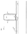
110 半導体基板
120 ソース電極
125 ドレイン電極
140 チャネル領域
150 絶縁体ゲート
210 シリコン基板
220 遮蔽酸化物
310 絶縁体ゲート
320 ゲート電極
Claims (25)
- 電流の流れを調節するためのデバイスを製造する方法であって、
半導体基板を与え、
前記半導体基板上にゲート電極を与え、
前記ゲート電極に隣接する領域の前記半導体基板を露出し、
部分的な等方性エッチングを使って前記露出した領域上の半導体基板をエッチングし、
前記半導体基板のエッチングされた領域に金属の薄膜を蒸着し、
前記金属を前記基板に反応させてショットキー又はショットキーの様なソース電極又はドレイン電極を形成することを含む方法。 - 請求項1記載の方法において、前記半導体基板は、シリコン、ひずみシリコン、シリコン・オン・インシュレーター、シリコンゲルマニウム、ガリウムヒ素、又は、リン化インジウム、を含む方法。
- 請求項1記載の方法において、前記エッチング動作は、縦方向のエッチング速度の約10分の1から10倍の横方向のエッチング速度を有するエッチングを使って実行される方法。
- 請求項1記載の方法において、
前記部分的な等方性エッチングは前記半導体基板の縦方向のエッチング速度と前記半導体基板の横方向のエッチング速度とを含み、
前記縦方向のエッチング速度は前記横方向のエッチング速度の略10倍である方法。 - 請求項1記載の方法において、
前記部分的な等方性エッチングは前記半導体基板の横方向のエッチング速度と前記半導体基板の縦方向のエッチング速度とを含み、
前記横方向のエッチング速度は前記縦横方向のエッチング速度の略10倍である方法。 - 請求項1記載の方法において、
前記部分的な等方性エッチングは前記半導体基板の横方向のエッチング速度と前記半導体基板の縦方向のエッチング速度とを含み、
前記横方向及び縦方向のエッチング速度は略同じである方法。 - 請求項1記載の方法において、
前記半導体基板上に薄い絶縁層を与え、
前記絶縁層上に導電性薄膜を蒸着し、
前記導電性膜にパターニング及びエッチングをしてゲート電極を形成し、
前記ゲート電極の一又はそれ以上の側壁に一又はそれ以上の薄い絶縁層を形成する
ことからなるステップによって前記ゲート電極が与えられる方法。 - 請求項1記載の方法において、前記ショットキー又はショットキーの様なソース及びドレイン電極を形成した後、前記デバイスから未反応の金属を取り除くことをさらに含む方法。
- 請求項1記載の方法において、前記反応ステップはアニーリングによって実行される方法。
- 請求項1記載の方法において、前記ソース電極及びドレイン電極は、白金シリサイド、パラジウムケイ素化合物、イリジウムケイ素化合物のうちのいずか一つ又はそれらの組み合わせである方法。
- 請求項1記載の方法において、前記ソース電極及びドレイン電極は希土類ケイ素化合物である方法。
- 請求項1記載の方法において、ショットキー又はショットキーの様な接触は、少なくとも前記ゲート電極の下のチャネル区域に近接した領域において形成される方法。
- 請求項1記載の方法において、ソース電極及びドレイン電極の少なくとも一つの全体の表面が、前記半導体基板とのショットキー又はショットキーの様な接触を形成する方法。
- 請求項1記載の方法において、
前記ゲート電極を与える動作の前に前記半導体基板の中に不純物が導入され、
前記ソース及びドレイン電極間のチャネル領域中の不純物は、ヒ素、リン、又は、アンチモンを含む方法。 - 請求項1記載の方法において、
前記ゲート電極を与える動作の前に前記半導体基板の中に不純物が導入され、
前記ソース及びドレイン電極間のチャネル領域中の不純物は、ボロン、インジウム、又は、ガリウムを含む方法。 - 請求項14記載の方法において、前記半導体基板は、縦方向においては有意に変化して横方向には略一定の、チャネル不純物濃度を有する方法。
- 請求項14記載の方法において、前記半導体基板は、縦方向及び横方向において有意に変化するチャネル不純物濃度を有する方法。
- 請求項15記載の方法において、前記半導体基板は、縦方向においては有意に変化して横方向には略一定の、チャネル不純物濃度を有する方法。
- 請求項15記載の方法において、前記半導体基板は、縦方向及び横方向において有意に変化するチャネル不純物濃度を有する方法。
- 電流の流れを調節するためのデバイスを製造する方法であって、
ゲート電極に隣接する領域における半導体基板を露出し、
部分的な等方性エッチングを使って前記露出した領域上の半導体基板をエッチングし、
前記半導体基板に金属薄膜を蒸着し、アニーリングし、ショットキー又はショットキーの様なソース電極又はドレイン電極を形成する方法。 - 請求項20記載の方法において、
前記部分的な等方性エッチングは前記半導体基板の縦方向のエッチング速度と前記半導体基板の横方向のエッチング速度とを含み、
前記縦方向のエッチング速度は前記横方向のエッチング速度の略10倍である方法。 - 請求項20記載の方法において、
前記部分的な等方性エッチングは前記半導体基板の横方向のエッチング速度と前記半導体基板の縦方向のエッチング速度とを含み、
前記横方向のエッチング速度は前記縦方向のエッチング速度の略10倍である方法。 - 請求項20記載の方法において、
前記部分的な等方性エッチングは前記半導体基板の横方向のエッチング速度と前記半導体基板の縦方向のエッチング速度とを含み、
前記横方向及び縦方向のエッチング速度は略同じである方法。 - 請求項20記載の方法において、前記エッチング動作は、縦方向のエッチング速度の約10分の1から10倍の横方向のエッチング速度を有するエッチングを使って実行される方法。
- 請求項20記載の方法において、前記半導体基板は、前記蒸着ステップの間加熱されて前記半導体基板中に金属原子が拡散することを促進する方法。
Applications Claiming Priority (2)
| Application Number | Priority Date | Filing Date | Title |
|---|---|---|---|
| US50914203P | 2003-10-03 | 2003-10-03 | |
| PCT/US2004/032539 WO2005036631A1 (en) | 2003-10-03 | 2004-10-04 | Schottky-barrier mosfet manufacturing method using isotropic etch process |
Publications (2)
| Publication Number | Publication Date |
|---|---|
| JP2007507905A true JP2007507905A (ja) | 2007-03-29 |
| JP2007507905A5 JP2007507905A5 (ja) | 2007-11-22 |
Family
ID=34434946
Family Applications (1)
| Application Number | Title | Priority Date | Filing Date |
|---|---|---|---|
| JP2006534203A Pending JP2007507905A (ja) | 2003-10-03 | 2004-10-04 | 等方性エッチングプロセスを使ったショットキーバリアmosfet製造方法 |
Country Status (6)
| Country | Link |
|---|---|
| US (1) | US7291524B2 (ja) |
| EP (1) | EP1676305A1 (ja) |
| JP (1) | JP2007507905A (ja) |
| CN (1) | CN1868045A (ja) |
| RU (1) | RU2006114833A (ja) |
| WO (1) | WO2005036631A1 (ja) |
Families Citing this family (32)
| Publication number | Priority date | Publication date | Assignee | Title |
|---|---|---|---|---|
| US6303479B1 (en) * | 1999-12-16 | 2001-10-16 | Spinnaker Semiconductor, Inc. | Method of manufacturing a short-channel FET with Schottky-barrier source and drain contacts |
| US7393733B2 (en) | 2004-12-01 | 2008-07-01 | Amberwave Systems Corporation | Methods of forming hybrid fin field-effect transistor structures |
| KR100560432B1 (ko) * | 2004-12-21 | 2006-03-13 | 한국전자통신연구원 | N형 쇼트키 장벽 관통 트랜지스터 소자 및 제조 방법 |
| US8324660B2 (en) | 2005-05-17 | 2012-12-04 | Taiwan Semiconductor Manufacturing Company, Ltd. | Lattice-mismatched semiconductor structures with reduced dislocation defect densities and related methods for device fabrication |
| US9153645B2 (en) | 2005-05-17 | 2015-10-06 | Taiwan Semiconductor Manufacturing Company, Ltd. | Lattice-mismatched semiconductor structures with reduced dislocation defect densities and related methods for device fabrication |
| US8658053B2 (en) * | 2005-06-24 | 2014-02-25 | Mitsubishi Gas Chemical Company, Inc. | Etching composition for metal material and method for manufacturing semiconductor device by using same |
| US7816240B2 (en) * | 2006-02-23 | 2010-10-19 | Acorn Technologies, Inc. | Method for making semiconductor insulated-gate field-effect transistor having multilayer deposited metal source(s) and/or drain(s) |
| WO2007112066A2 (en) | 2006-03-24 | 2007-10-04 | Amberwave Systems Corporation | Lattice-mismatched semiconductor structures and related methods for device fabrication |
| US8173551B2 (en) | 2006-09-07 | 2012-05-08 | Taiwan Semiconductor Manufacturing Co., Ltd. | Defect reduction using aspect ratio trapping |
| US7799592B2 (en) | 2006-09-27 | 2010-09-21 | Taiwan Semiconductor Manufacturing Company, Ltd. | Tri-gate field-effect transistors formed by aspect ratio trapping |
| US7875958B2 (en) | 2006-09-27 | 2011-01-25 | Taiwan Semiconductor Manufacturing Company, Ltd. | Quantum tunneling devices and circuits with lattice-mismatched semiconductor structures |
| WO2008051503A2 (en) | 2006-10-19 | 2008-05-02 | Amberwave Systems Corporation | Light-emitter-based devices with lattice-mismatched semiconductor structures |
| US7825328B2 (en) | 2007-04-09 | 2010-11-02 | Taiwan Semiconductor Manufacturing Company, Ltd. | Nitride-based multi-junction solar cell modules and methods for making the same |
| US8237151B2 (en) | 2009-01-09 | 2012-08-07 | Taiwan Semiconductor Manufacturing Company, Ltd. | Diode-based devices and methods for making the same |
| US8304805B2 (en) | 2009-01-09 | 2012-11-06 | Taiwan Semiconductor Manufacturing Company, Ltd. | Semiconductor diodes fabricated by aspect ratio trapping with coalesced films |
| US9508890B2 (en) | 2007-04-09 | 2016-11-29 | Taiwan Semiconductor Manufacturing Company, Ltd. | Photovoltaics on silicon |
| US7553717B2 (en) * | 2007-05-11 | 2009-06-30 | Texas Instruments Incorporated | Recess etch for epitaxial SiGe |
| US8329541B2 (en) | 2007-06-15 | 2012-12-11 | Taiwan Semiconductor Manufacturing Company, Ltd. | InP-based transistor fabrication |
| DE112008002387B4 (de) | 2007-09-07 | 2022-04-07 | Taiwan Semiconductor Manufacturing Co., Ltd. | Struktur einer Mehrfachübergangs-Solarzelle, Verfahren zur Bildung einer photonischenVorrichtung, Photovoltaische Mehrfachübergangs-Zelle und Photovoltaische Mehrfachübergangs-Zellenvorrichtung, |
| US8183667B2 (en) | 2008-06-03 | 2012-05-22 | Taiwan Semiconductor Manufacturing Co., Ltd. | Epitaxial growth of crystalline material |
| US8274097B2 (en) | 2008-07-01 | 2012-09-25 | Taiwan Semiconductor Manufacturing Company, Ltd. | Reduction of edge effects from aspect ratio trapping |
| US8981427B2 (en) | 2008-07-15 | 2015-03-17 | Taiwan Semiconductor Manufacturing Company, Ltd. | Polishing of small composite semiconductor materials |
| US20100072515A1 (en) | 2008-09-19 | 2010-03-25 | Amberwave Systems Corporation | Fabrication and structures of crystalline material |
| WO2010033813A2 (en) | 2008-09-19 | 2010-03-25 | Amberwave System Corporation | Formation of devices by epitaxial layer overgrowth |
| US8253211B2 (en) | 2008-09-24 | 2012-08-28 | Taiwan Semiconductor Manufacturing Company, Ltd. | Semiconductor sensor structures with reduced dislocation defect densities |
| CN102379046B (zh) | 2009-04-02 | 2015-06-17 | 台湾积体电路制造股份有限公司 | 从晶体材料的非极性平面形成的器件及其制作方法 |
| US8513765B2 (en) | 2010-07-19 | 2013-08-20 | International Business Machines Corporation | Formation method and structure for a well-controlled metallic source/drain semiconductor device |
| US9691898B2 (en) * | 2013-12-19 | 2017-06-27 | Taiwan Semiconductor Manufacturing Co., Ltd. | Germanium profile for channel strain |
| CN103745929A (zh) * | 2013-12-24 | 2014-04-23 | 上海新傲科技股份有限公司 | 肖特基势垒mosfet的制备方法 |
| JP6697909B2 (ja) * | 2016-03-15 | 2020-05-27 | エイブリック株式会社 | 半導体装置とその製造方法 |
| US10249542B2 (en) * | 2017-01-12 | 2019-04-02 | International Business Machines Corporation | Self-aligned doping in source/drain regions for low contact resistance |
| RU2688861C1 (ru) * | 2018-03-12 | 2019-05-22 | Федеральное государственное бюджетное образовательное учреждение высшего образования "Кабардино-Балкарский государственный университет им. Х.М. Бербекова" (КБГУ) | Способ изготовления полупроводникового прибора |
Citations (2)
| Publication number | Priority date | Publication date | Assignee | Title |
|---|---|---|---|---|
| JPS61237470A (ja) * | 1985-04-15 | 1986-10-22 | Hitachi Ltd | 半導体装置 |
| JP2003517210A (ja) * | 1999-12-16 | 2003-05-20 | スピネカ セミコンダクター, インコーポレイテッド | Mosfetデバイスのシステムおよび方法 |
Family Cites Families (6)
| Publication number | Priority date | Publication date | Assignee | Title |
|---|---|---|---|---|
| US5834793A (en) * | 1985-12-27 | 1998-11-10 | Kabushiki Kaisha Toshiba | Semiconductor devices |
| JP3761918B2 (ja) * | 1994-09-13 | 2006-03-29 | 株式会社東芝 | 半導体装置の製造方法 |
| US6949787B2 (en) | 2001-08-10 | 2005-09-27 | Spinnaker Semiconductor, Inc. | Transistor having high dielectric constant gate insulating layer and source and drain forming Schottky contact with substrate |
| JP3833903B2 (ja) * | 2000-07-11 | 2006-10-18 | 株式会社東芝 | 半導体装置の製造方法 |
| EP1468440A2 (en) | 2002-01-23 | 2004-10-20 | Spinnaker Semiconductor, Inc. | Field effect transistor having source and/or drain forming schottky or schottky−like contact with strained semiconductor substrate |
| US6974737B2 (en) | 2002-05-16 | 2005-12-13 | Spinnaker Semiconductor, Inc. | Schottky barrier CMOS fabrication method |
-
2004
- 2004-10-04 JP JP2006534203A patent/JP2007507905A/ja active Pending
- 2004-10-04 CN CNA200480028742XA patent/CN1868045A/zh active Pending
- 2004-10-04 RU RU2006114833/28A patent/RU2006114833A/ru not_active Application Discontinuation
- 2004-10-04 WO PCT/US2004/032539 patent/WO2005036631A1/en active Application Filing
- 2004-10-04 US US10/957,913 patent/US7291524B2/en not_active Expired - Fee Related
- 2004-10-04 EP EP04794042A patent/EP1676305A1/en not_active Withdrawn
Patent Citations (2)
| Publication number | Priority date | Publication date | Assignee | Title |
|---|---|---|---|---|
| JPS61237470A (ja) * | 1985-04-15 | 1986-10-22 | Hitachi Ltd | 半導体装置 |
| JP2003517210A (ja) * | 1999-12-16 | 2003-05-20 | スピネカ セミコンダクター, インコーポレイテッド | Mosfetデバイスのシステムおよび方法 |
Also Published As
| Publication number | Publication date |
|---|---|
| CN1868045A (zh) | 2006-11-22 |
| WO2005036631A1 (en) | 2005-04-21 |
| US20050118793A1 (en) | 2005-06-02 |
| RU2006114833A (ru) | 2007-11-10 |
| US7291524B2 (en) | 2007-11-06 |
| EP1676305A1 (en) | 2006-07-05 |
Similar Documents
| Publication | Publication Date | Title |
|---|---|---|
| JP2007507905A (ja) | 等方性エッチングプロセスを使ったショットキーバリアmosfet製造方法 | |
| US7701010B2 (en) | Method of fabricating transistor including buried insulating layer and transistor fabricated using the same | |
| US8058167B2 (en) | Dynamic Schottky barrier MOSFET device and method of manufacture | |
| US9281390B2 (en) | Structure and method for forming programmable high-K/metal gate memory device | |
| US8022459B2 (en) | Metal source and drain transistor having high dielectric constant gate insulator | |
| JP4110085B2 (ja) | 二重ゲート型電界効果トランジスタの製造方法 | |
| US20070194353A1 (en) | Metal source/drain Schottky barrier silicon-on-nothing MOSFET device and method thereof | |
| JP2005516389A (ja) | 歪み半導体基板を用いてショットキまたはショットキのような接触を形成するソースおよび/またはドレインを有する電界効果トランジスタ | |
| KR20080058341A (ko) | 낮은 밀러 용량 및 향상된 구동 전류를 위한 단일 게이트상의 다중 저유전율 및 고유전율 게이트 산화막 | |
| US20050009285A1 (en) | Semiconductor component and method of manufacture | |
| JP3874716B2 (ja) | 半導体装置の製造方法 | |
| US20080070356A1 (en) | Trench replacement gate process for transistors having elevated source and drain regions | |
| US7148096B2 (en) | Method of manufacturing a semiconductor device having a gate electrode containing polycrystalline silicon-germanium | |
| JP4110089B2 (ja) | 二重ゲート型電界効果トランジスタの製造方法 | |
| KR100586178B1 (ko) | 쇼트키 장벽 관통 트랜지스터 및 그 제조방법 | |
| US20060079059A1 (en) | Transistor having high dielectric constant gate insulating layer and source and drain forming schottky contact with substrate | |
| KR100579854B1 (ko) | 반도체 소자의 게이트 전극 형성 방법 | |
| JP2004031529A (ja) | 半導体装置及びその製造方法 | |
| JPH06334135A (ja) | 相補型misトランジスタの製造方法 |
Legal Events
| Date | Code | Title | Description |
|---|---|---|---|
| A521 | Written amendment |
Free format text: JAPANESE INTERMEDIATE CODE: A523 Effective date: 20071004 |
|
| A621 | Written request for application examination |
Free format text: JAPANESE INTERMEDIATE CODE: A621 Effective date: 20071004 |
|
| A977 | Report on retrieval |
Free format text: JAPANESE INTERMEDIATE CODE: A971007 Effective date: 20110526 |
|
| A131 | Notification of reasons for refusal |
Free format text: JAPANESE INTERMEDIATE CODE: A131 Effective date: 20110606 |
|
| A02 | Decision of refusal |
Free format text: JAPANESE INTERMEDIATE CODE: A02 Effective date: 20111031 |