WO2009119664A1 - Dispositif d'affichage à détecteur tactile - Google Patents
Dispositif d'affichage à détecteur tactile Download PDFInfo
- Publication number
- WO2009119664A1 WO2009119664A1 PCT/JP2009/055949 JP2009055949W WO2009119664A1 WO 2009119664 A1 WO2009119664 A1 WO 2009119664A1 JP 2009055949 W JP2009055949 W JP 2009055949W WO 2009119664 A1 WO2009119664 A1 WO 2009119664A1
- Authority
- WO
- WIPO (PCT)
- Prior art keywords
- electrode
- display
- touch sensor
- touch
- display device
- Prior art date
Links
Images


Classifications
-
- G—PHYSICS
- G02—OPTICS
- G02F—OPTICAL DEVICES OR ARRANGEMENTS FOR THE CONTROL OF LIGHT BY MODIFICATION OF THE OPTICAL PROPERTIES OF THE MEDIA OF THE ELEMENTS INVOLVED THEREIN; NON-LINEAR OPTICS; FREQUENCY-CHANGING OF LIGHT; OPTICAL LOGIC ELEMENTS; OPTICAL ANALOGUE/DIGITAL CONVERTERS
- G02F1/00—Devices or arrangements for the control of the intensity, colour, phase, polarisation or direction of light arriving from an independent light source, e.g. switching, gating or modulating; Non-linear optics
- G02F1/01—Devices or arrangements for the control of the intensity, colour, phase, polarisation or direction of light arriving from an independent light source, e.g. switching, gating or modulating; Non-linear optics for the control of the intensity, phase, polarisation or colour
- G02F1/13—Devices or arrangements for the control of the intensity, colour, phase, polarisation or direction of light arriving from an independent light source, e.g. switching, gating or modulating; Non-linear optics for the control of the intensity, phase, polarisation or colour based on liquid crystals, e.g. single liquid crystal display cells
- G02F1/133—Constructional arrangements; Operation of liquid crystal cells; Circuit arrangements
- G02F1/1333—Constructional arrangements; Manufacturing methods
- G02F1/13338—Input devices, e.g. touch panels
-
- G—PHYSICS
- G06—COMPUTING; CALCULATING OR COUNTING
- G06F—ELECTRIC DIGITAL DATA PROCESSING
- G06F3/00—Input arrangements for transferring data to be processed into a form capable of being handled by the computer; Output arrangements for transferring data from processing unit to output unit, e.g. interface arrangements
- G06F3/01—Input arrangements or combined input and output arrangements for interaction between user and computer
- G06F3/03—Arrangements for converting the position or the displacement of a member into a coded form
- G06F3/041—Digitisers, e.g. for touch screens or touch pads, characterised by the transducing means
- G06F3/0412—Digitisers structurally integrated in a display
-
- G—PHYSICS
- G02—OPTICS
- G02F—OPTICAL DEVICES OR ARRANGEMENTS FOR THE CONTROL OF LIGHT BY MODIFICATION OF THE OPTICAL PROPERTIES OF THE MEDIA OF THE ELEMENTS INVOLVED THEREIN; NON-LINEAR OPTICS; FREQUENCY-CHANGING OF LIGHT; OPTICAL LOGIC ELEMENTS; OPTICAL ANALOGUE/DIGITAL CONVERTERS
- G02F1/00—Devices or arrangements for the control of the intensity, colour, phase, polarisation or direction of light arriving from an independent light source, e.g. switching, gating or modulating; Non-linear optics
- G02F1/01—Devices or arrangements for the control of the intensity, colour, phase, polarisation or direction of light arriving from an independent light source, e.g. switching, gating or modulating; Non-linear optics for the control of the intensity, phase, polarisation or colour
- G02F1/13—Devices or arrangements for the control of the intensity, colour, phase, polarisation or direction of light arriving from an independent light source, e.g. switching, gating or modulating; Non-linear optics for the control of the intensity, phase, polarisation or colour based on liquid crystals, e.g. single liquid crystal display cells
- G02F1/133—Constructional arrangements; Operation of liquid crystal cells; Circuit arrangements
- G02F1/1333—Constructional arrangements; Manufacturing methods
- G02F1/1343—Electrodes
- G02F1/134309—Electrodes characterised by their geometrical arrangement
- G02F1/134363—Electrodes characterised by their geometrical arrangement for applying an electric field parallel to the substrate, i.e. in-plane switching [IPS]
-
- G—PHYSICS
- G06—COMPUTING; CALCULATING OR COUNTING
- G06F—ELECTRIC DIGITAL DATA PROCESSING
- G06F3/00—Input arrangements for transferring data to be processed into a form capable of being handled by the computer; Output arrangements for transferring data from processing unit to output unit, e.g. interface arrangements
- G06F3/01—Input arrangements or combined input and output arrangements for interaction between user and computer
- G06F3/03—Arrangements for converting the position or the displacement of a member into a coded form
- G06F3/041—Digitisers, e.g. for touch screens or touch pads, characterised by the transducing means
- G06F3/044—Digitisers, e.g. for touch screens or touch pads, characterised by the transducing means by capacitive means
- G06F3/0443—Digitisers, e.g. for touch screens or touch pads, characterised by the transducing means by capacitive means using a single layer of sensing electrodes
-
- G—PHYSICS
- G06—COMPUTING; CALCULATING OR COUNTING
- G06F—ELECTRIC DIGITAL DATA PROCESSING
- G06F3/00—Input arrangements for transferring data to be processed into a form capable of being handled by the computer; Output arrangements for transferring data from processing unit to output unit, e.g. interface arrangements
- G06F3/01—Input arrangements or combined input and output arrangements for interaction between user and computer
- G06F3/03—Arrangements for converting the position or the displacement of a member into a coded form
- G06F3/041—Digitisers, e.g. for touch screens or touch pads, characterised by the transducing means
- G06F3/044—Digitisers, e.g. for touch screens or touch pads, characterised by the transducing means by capacitive means
- G06F3/0445—Digitisers, e.g. for touch screens or touch pads, characterised by the transducing means by capacitive means using two or more layers of sensing electrodes, e.g. using two layers of electrodes separated by a dielectric layer
-
- G—PHYSICS
- G06—COMPUTING; CALCULATING OR COUNTING
- G06F—ELECTRIC DIGITAL DATA PROCESSING
- G06F3/00—Input arrangements for transferring data to be processed into a form capable of being handled by the computer; Output arrangements for transferring data from processing unit to output unit, e.g. interface arrangements
- G06F3/01—Input arrangements or combined input and output arrangements for interaction between user and computer
- G06F3/03—Arrangements for converting the position or the displacement of a member into a coded form
- G06F3/041—Digitisers, e.g. for touch screens or touch pads, characterised by the transducing means
- G06F3/044—Digitisers, e.g. for touch screens or touch pads, characterised by the transducing means by capacitive means
- G06F3/0446—Digitisers, e.g. for touch screens or touch pads, characterised by the transducing means by capacitive means using a grid-like structure of electrodes in at least two directions, e.g. using row and column electrodes
-
- G—PHYSICS
- G02—OPTICS
- G02F—OPTICAL DEVICES OR ARRANGEMENTS FOR THE CONTROL OF LIGHT BY MODIFICATION OF THE OPTICAL PROPERTIES OF THE MEDIA OF THE ELEMENTS INVOLVED THEREIN; NON-LINEAR OPTICS; FREQUENCY-CHANGING OF LIGHT; OPTICAL LOGIC ELEMENTS; OPTICAL ANALOGUE/DIGITAL CONVERTERS
- G02F1/00—Devices or arrangements for the control of the intensity, colour, phase, polarisation or direction of light arriving from an independent light source, e.g. switching, gating or modulating; Non-linear optics
- G02F1/01—Devices or arrangements for the control of the intensity, colour, phase, polarisation or direction of light arriving from an independent light source, e.g. switching, gating or modulating; Non-linear optics for the control of the intensity, phase, polarisation or colour
- G02F1/13—Devices or arrangements for the control of the intensity, colour, phase, polarisation or direction of light arriving from an independent light source, e.g. switching, gating or modulating; Non-linear optics for the control of the intensity, phase, polarisation or colour based on liquid crystals, e.g. single liquid crystal display cells
- G02F1/133—Constructional arrangements; Operation of liquid crystal cells; Circuit arrangements
- G02F1/1333—Constructional arrangements; Manufacturing methods
- G02F1/1343—Electrodes
- G02F1/134309—Electrodes characterised by their geometrical arrangement
- G02F1/134372—Electrodes characterised by their geometrical arrangement for fringe field switching [FFS] where the common electrode is not patterned
-
- G—PHYSICS
- G02—OPTICS
- G02F—OPTICAL DEVICES OR ARRANGEMENTS FOR THE CONTROL OF LIGHT BY MODIFICATION OF THE OPTICAL PROPERTIES OF THE MEDIA OF THE ELEMENTS INVOLVED THEREIN; NON-LINEAR OPTICS; FREQUENCY-CHANGING OF LIGHT; OPTICAL LOGIC ELEMENTS; OPTICAL ANALOGUE/DIGITAL CONVERTERS
- G02F2201/00—Constructional arrangements not provided for in groups G02F1/00 - G02F7/00
- G02F2201/12—Constructional arrangements not provided for in groups G02F1/00 - G02F7/00 electrode
-
- G—PHYSICS
- G06—COMPUTING; CALCULATING OR COUNTING
- G06F—ELECTRIC DIGITAL DATA PROCESSING
- G06F2203/00—Indexing scheme relating to G06F3/00 - G06F3/048
- G06F2203/041—Indexing scheme relating to G06F3/041 - G06F3/045
- G06F2203/04107—Shielding in digitiser, i.e. guard or shielding arrangements, mostly for capacitive touchscreens, e.g. driven shields, driven grounds
-
- G—PHYSICS
- G09—EDUCATION; CRYPTOGRAPHY; DISPLAY; ADVERTISING; SEALS
- G09G—ARRANGEMENTS OR CIRCUITS FOR CONTROL OF INDICATING DEVICES USING STATIC MEANS TO PRESENT VARIABLE INFORMATION
- G09G3/00—Control arrangements or circuits, of interest only in connection with visual indicators other than cathode-ray tubes
- G09G3/20—Control arrangements or circuits, of interest only in connection with visual indicators other than cathode-ray tubes for presentation of an assembly of a number of characters, e.g. a page, by composing the assembly by combination of individual elements arranged in a matrix no fixed position being assigned to or needed to be assigned to the individual characters or partial characters
- G09G3/34—Control arrangements or circuits, of interest only in connection with visual indicators other than cathode-ray tubes for presentation of an assembly of a number of characters, e.g. a page, by composing the assembly by combination of individual elements arranged in a matrix no fixed position being assigned to or needed to be assigned to the individual characters or partial characters by control of light from an independent source
- G09G3/36—Control arrangements or circuits, of interest only in connection with visual indicators other than cathode-ray tubes for presentation of an assembly of a number of characters, e.g. a page, by composing the assembly by combination of individual elements arranged in a matrix no fixed position being assigned to or needed to be assigned to the individual characters or partial characters by control of light from an independent source using liquid crystals
- G09G3/3611—Control of matrices with row and column drivers
- G09G3/3648—Control of matrices with row and column drivers using an active matrix
Definitions
- the present invention relates to a display device such as a liquid crystal display device, and more particularly to a display device with a touch sensor including a capacitive touch sensor capable of inputting information when a user touches with a finger or the like.
- a touch detection device (hereinafter referred to as a touch sensor) called a so-called touch panel is directly mounted on a liquid crystal display device, and various buttons are displayed on the liquid crystal display device to input information as a substitute for ordinary buttons. Attention has focused on display devices that have made it possible.
- This technology brings about the big merit of space saving and reduction of the number of parts from enabling the common use of the arrangement of a display and a button in the tendency of a screen of a mobile device to become large.
- this technique has a problem in that the thickness of the whole liquid crystal module is increased by the attachment of the touch panel.
- the liquid crystal module tends to be thicker, which is against the trend of thinning.
- Patent Document 1 a conductive film for a touch panel is provided between the observation side substrate of the liquid crystal display element and the observation polarizing plate disposed on the outer surface thereof, and the conductive film for the touch panel and the outer surface of the polarizing plate.
- a liquid crystal display element with a touch panel in which a capacitive touch panel with the outer surface of the polarizing plate as the touch surface is formed has been proposed, and thinning has been achieved.
- the touch panel conductive film needs to be at the same potential as the user, and the user needs to be properly grounded. . Therefore, it is practically difficult to apply to mobile device applications, apart from stationary television receivers that are powered from a wall outlet. Further, in the above technology, the conductive film for a touch panel needs to be extremely close to the user's finger, so that it is impossible to dispose the liquid crystal display element in, for example, a deep portion, and the arrangement site is limited. Ru. That is, the degree of freedom in design is small. Furthermore, in the above technology, it is necessary to provide circuits such as a touch panel drive unit and a coordinate detection unit separately from the display drive circuit unit of the liquid crystal display element due to the configuration, and circuit integration as the entire device is difficult It is.
- the present invention has been made in view of such problems, and a first object of the present invention is to provide a display device with a touch sensor which is particularly suitable for mobile device applications.
- the second object is to provide a display device with a touch sensor with a high degree of freedom in design.
- a third object of the present invention is to provide a display device with a touch sensor having a structure in which circuit integration is easy.
- the display device with a touch sensor includes a plurality of display pixel electrodes, a common electrode provided opposite to the display pixel electrodes, a display functional layer having an image display function, and a display pixel electrode based on an image signal.
- a display control circuit that performs image display control so that a display voltage is applied between the common electrode and the display function of the display functional layer; and a display control circuit provided opposite to or in line with the common electrode And a touch detection electrode for forming a capacitance therebetween.
- a capacitance is formed between the common electrode originally provided for applying the display driving voltage and the newly provided touch detection electrode.
- the capacitance changes depending on the presence or absence of contact of the object. Therefore, if the display drive voltage applied to the common electrode by the display control unit is also used (shared) as a drive signal for touch sensor, a detection signal corresponding to the change in capacitance is obtained from the touch detection electrode. Be Then, if the detection signal is input to the touch detection circuit, the presence or absence of the touch of the object can be detected. Furthermore, when the touch detection electrodes are divided into a plurality of electrode patterns and individually driven, the contact position of the object can be detected.
- the display functional layer for example, a liquid crystal layer is used.
- the opposing substrate is disposed to face the circuit substrate on which the display control circuit is formed, and the display pixel electrode is disposed on the circuit substrate near the opposing substrate and the common electrode is disposed. It is possible to dispose the display functional layer on the side closer to the circuit substrate of the counter substrate and to interpose the display functional layer between the display pixel electrode of the circuit substrate and the common electrode of the counter substrate.
- the display functional layer is, for example, a liquid crystal such as a TN (twisted nematic) mode or a VA (vertical alignment) mode.
- the touch detection electrode is preferably formed on the counter substrate side, and the touch detection circuit is preferably formed on the circuit substrate.
- the counter substrate is disposed to face the circuit substrate on which the display control circuit is formed, and the common electrode and the display pixel electrode are sequentially stacked on the circuit substrate through the insulating layer.
- the display functional layer may be inserted between the display pixel electrode of the circuit substrate and the counter substrate. This configuration is suitable when the display functional layer is a liquid crystal in a so-called horizontal electric field mode such as FFS (fringe field switching) mode.
- the touch detection electrode may be formed on the counter substrate side or may be formed on the circuit substrate side.
- the touch detection circuit is preferably formed on a circuit board.
- the common electrode is disposed inside the display area of the circuit board, and the touch detection electrode is formed in the frame area on the circuit board as an electrode layer in the same layer as the common electrode. It is also possible to form so as to be separated from the common electrode.
- the touch detection electrode is formed on the counter substrate side and the touch detection circuit is formed on the circuit substrate, the conductive connection between the touch detection electrode on the counter substrate side and the touch detection circuit on the circuit substrate side It suffices to form a route.
- a capacitive coupling path may be formed to capacitively couple between the touch detection electrode on the opposite substrate side and the touch detection circuit on the circuit substrate side.
- an electrostatic capacitance is formed between the common electrode originally provided for application of the display drive voltage and the newly provided touch detection electrode, and this electrostatic capacitance is formed. Since touch detection is performed using the fact that the capacity is changed by the touch of an object (user's finger), it has a touch sensor that can be adapted to mobile device applications where the user's potential is often indeterminate. A display can be obtained.
- the existing display drive voltage originally prepared to be applied to the common electrode for display is also used (shared) as a drive signal for a touch sensor, a detection signal corresponding to a change in capacitance Since it is obtained from the touch detection electrode, it is not necessary to prepare a new sensor drive signal. Furthermore, if the touch detection electrodes are divided into a plurality of electrode patterns and individually driven, detection of the touch position is also possible.
- the display device with a touch sensor of the present invention whether to form the touch detection electrode on the counter substrate side or the pixel substrate side can be appropriately selected depending on the type of the display functional layer.
- the present invention can provide a display device with a touch sensor with a high degree of freedom in design.
- the display device with a touch sensor of the present invention it is possible to form the touch detection electrode on the circuit board side depending on the type of the display functional layer, so forming the touch detection circuit on the circuit board
- the circuit for display and the circuit for sensor can be easily integrated on one circuit board. That is, circuit integration is easy.
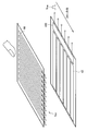
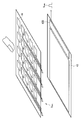
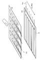
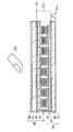
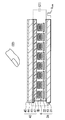
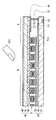
- FIG. 1 It is a perspective view which shows one structural example of the principal part (a common electrode and the detection electrode for sensors) of a display apparatus with a touch sensor shown in FIG. It is a circuit diagram which shows one structural example of the detection circuit in the display apparatus with a touch sensor shown in FIG. It is a perspective view which shows the other structural example of the principal part (common electrode and detection electrode for sensors) of the display apparatus with a touch sensor shown in FIG. It is a perspective view which shows the further another structural example of the principal part (common electrode and detection electrode for sensors) of the display apparatus with a touch sensor shown in FIG. It is sectional drawing showing the schematic cross-section of the display apparatus with a touch sensor which concerns on the 2nd Embodiment of this invention.
- FIG. It is an expansion perspective view of the principal part of the display apparatus with a touch sensor shown in FIG. It is sectional drawing for demonstrating the operation
- FIG. 1 It is a top view which shows the general
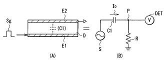
- This touch detection method is embodied as a capacitive touch sensor, and as shown in FIG. 1A, a pair of electrodes (drive electrode E1) disposed to face each other with a dielectric D interposed therebetween. And the detection electrode E2) to constitute a capacitive element.
- This structure is expressed as an equivalent circuit shown in FIG.
- the drive electrode E1, the detection electrode E2 and the dielectric D constitute a capacitive element C1.
- One end of the capacitive element C1 is connected to the AC signal source S, and the other end P is grounded via the resistor R and is connected to the voltage detector DET.
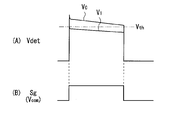
- an alternating current rectangular wave Sg (FIG. 3B) of a predetermined frequency (for example, several kHz to about several tens of kHz) is applied from the alternating current signal source S to the drive electrode E1 (one end of the capacitive element C1), the detection electrode E2 (capacitance The output waveform (detection signal Vdet) as shown in FIG. 3A appears at the other end P) of the element C1.
- the AC rectangular wave Sg corresponds to a common drive signal Vcom described later.
- a current I0 flows according to the capacitance value of the capacitive element C1 as the capacitive element C1 is charged and discharged.
- the potential waveform of the other end P of the capacitive element C1 at this time is, for example, as shown by a waveform V0 in FIG. 3A, and this is detected by the voltage detector DET.
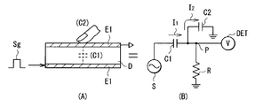
- the capacitive element C2 formed by the finger is added in series to the capacitive element C1.
- currents I1 and I2 flow as the capacitive elements C1 and C2 are charged and discharged.
- the potential waveform of the other end P of the capacitive element C1 at this time is, for example, like a waveform V1 of FIG. 3A, and this is detected by the voltage detector DET.
- the potential at the point P is a divided potential which is determined by the values of the currents I1 and I2 flowing through the capacitive elements C1 and C2. Therefore, the waveform V1 has a smaller value than the waveform V0 in the non-contact state.
- the voltage detector DET compares the detected voltage with a predetermined threshold voltage Vth, and determines that it is in the non-contact state if it is below this threshold voltage, while it is above the threshold voltage If it is determined that there is a touch condition. In this way, touch detection is possible.
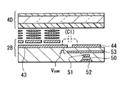
- FIG. 4 shows the cross-sectional structure of the main part of the display device with a touch sensor according to the present embodiment.
- the display device with a touch sensor uses a liquid crystal display element as a display element, and also a part of the electrodes originally provided in the liquid crystal display element (common electrode 43 described later) and a display drive signal (common drive signal described later) Vcom) is also used to constitute a capacitive touch sensor.
- the pixel substrate 2, the opposing substrate 4 disposed to face the pixel substrate 2, and the pixel substrate 2 and the opposing substrate 4 are interposed. And the liquid crystal layer 6.
- the pixel substrate 2 has a TFT substrate 21 as a circuit substrate and a plurality of pixel electrodes 22 arranged in a matrix on the TFT substrate 21.
- the TFT substrate 21 includes not only display drivers and TFTs (thin film transistors) (not shown) for driving the respective pixel electrodes 22, but also source lines for supplying pixel signals to the respective pixel electrodes and wirings such as gate lines for driving the respective TFTs. Is formed.
- the TFT substrate 21 may also be provided with a detection circuit (FIG. 6) for performing a touch detection operation described later.
- the counter substrate 4 has a glass substrate 41, a color filter 42 formed on one surface of the glass substrate 41, and a common electrode 43 formed on the color filter 42.
- the color filter 42 is formed by periodically arranging, for example, three color filter layers of red (R), green (G), and blue (B), and R is set for each display pixel (pixel electrode 22). , G, and B are associated as one set.
- the common electrode 43 is also used as a sensor drive electrode that constitutes a part of a touch sensor that performs a touch detection operation, and corresponds to the drive electrode E1 in FIG.
- the common electrode 43 is connected to the TFT substrate 21 by the contact conductive column 7.
- the common drive signal Vcom of an alternating current rectangular waveform is applied from the TFT substrate 21 to the common electrode 43 through the contact conductive pillar 7.
- the common drive signal Vcom defines the display voltage of each pixel together with the pixel voltage applied to the pixel electrode 22, but is also used as a drive signal of the touch sensor, and the drive signal source of FIG. It corresponds to the AC rectangular wave Sg supplied from S.
- a sensor detection electrode 44 is formed on the other surface of the glass substrate 41, and a polarizing plate 45 is disposed on the sensor detection electrode 44.
- the sensor detection electrode 44 constitutes a part of the touch sensor, and corresponds to the detection electrode E2 in FIG.
- the liquid crystal layer 6 modulates light passing therethrough according to the state of an electric field, and, for example, liquid crystals of various modes such as TN (twisted nematic), VA (vertical alignment), ECB (electric field control birefringence), etc. Is used.
- TN twisted nematic
- VA vertical alignment
- ECB electric field control birefringence
- alignment films are disposed between the liquid crystal layer 6 and the pixel substrate 2 and between the liquid crystal layer 6 and the counter substrate 4, respectively, and an incident side polarizing plate is provided on the lower surface side of the pixel substrate 2. Although arranged, illustration is omitted here.
- FIG. 5 is a perspective view of a configuration example of the common electrode 43 and the sensor detection electrode 44 in the counter substrate 4.
- the common electrode 43 is divided into a plurality of stripe-shaped electrode patterns extending in the lateral direction of the drawing.
- the common drive signal Vcom is sequentially supplied to each electrode pattern by the driver 43D, and line-sequential scan driving is performed in a time-division manner.
- the sensor detection electrode 44 is composed of a plurality of stripe-shaped electrode patterns extending in a direction orthogonal to the extending direction of the electrode pattern of the common electrode 43.
- a detection signal Vdet is output from each electrode pattern of the sensor detection electrode 44 and is input to the detection circuit 8 shown in FIG.
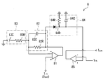
- FIG. 6 shows an example of the configuration of the detection circuit 8 that performs a touch detection operation.
- the detection circuit 8 includes an operational amplifier 81 for signal amplification, a low pass filter (LPF) 82 that cuts high frequencies and passes low frequencies, a high pass filter (HPF) 83 that passes high frequencies, a rectifying and smoothing unit 84 , And the comparator 85.
- An input terminal Tin is connected to the positive input terminal (+) of the operational amplifier 81, from which the detection signal Vdet is input.
- the output terminal of the operational amplifier 81 is connected to the rectifying and smoothing unit 84 via the LPF 82.
- An HPF 83 is connected to the LPF 82.
- the LPF 82 is a configuration in which a resistor 82R and a capacitor 82C are connected in parallel
- the HPF 83 is a configuration in which a resistor 83R and a capacitor 83C are connected in series between the resistor 82R and the ground.
- the connection point between the LPF 82 and the HPF 83 is connected to the negative input terminal ( ⁇ ) of the operational amplifier 81.
- Rectification smoothing part 84 includes a rectification part which consists of diode 84D for half wave rectification, and a smooth part which connects resistance 84R and capacitor 82C in parallel between grounding.
- the output terminal of the rectifying and smoothing unit 84 is connected to the positive input terminal (+) of the comparator 85.
- a predetermined threshold voltage Vth (see FIG. 3) is input to the negative input terminal (-) of the comparator 85.
- the output terminal of the comparator 85 is connected to the output terminal Tout, from which the detection result (whether touched or not) is output
- the detection circuit 8 having such a configuration operates as follows.
- the detection signal Vdet input to the input terminal Tin is amplified by the operational amplifier 81, and its low frequency component passes through the LPF 82, and the high frequency component is removed through the HPF 83.
- the low frequency AC component that has passed through the LPF 82 is half-wave rectified by the diode 84 D of the rectifying and smoothing unit 84 and then smoothed to be a level signal, which is input to the comparator 85.
- the comparator 85 compares the input level signal with the threshold voltage Vth, and outputs the touch detection signal when the level signal is equal to or lower than the threshold voltage Vth.
- the detection circuit 8 may be formed in the peripheral area (non-display area or frame area) on the counter substrate 4 or may be formed in the peripheral area on the pixel substrate 2. However, if formed on the pixel substrate 2, integration with various circuit elements and the like for display control originally formed on the pixel substrate 2 can be achieved, which is more preferable from the viewpoint of simplification by circuit integration. In this case, each electrode pattern of the sensor detection electrode 44 and the detection circuit 8 of the pixel substrate 2 are connected by a contact conductive column (not shown) similar to the contact conductive column 7, and the detection signal Vdet is output. The signal may be transmitted from the sensor detection electrode 44 to the detection circuit 8.
- a display driver (not shown) of the pixel substrate 2 supplies a common drive signal Vcom to each electrode pattern of the common electrode 43 line-sequentially.
- the display driver also supplies a pixel signal to the pixel electrode 22 through the source line and, in synchronization with this, line-sequentially controls switching of the TFT of each pixel electrode through the gate line.
- an electric field in the vertical direction (direction perpendicular to the substrate) determined by the common drive signal Vcom and each pixel signal is applied to the liquid crystal layer 6 to modulate the liquid crystal state. In this way, display by so-called inversion drive is performed.
- capacitive elements C 1 are formed at intersections between the electrode patterns of the common electrode 43 and the electrode patterns of the sensor detection electrode 44.
- the common drive signal Vcom is sequentially applied to each electrode pattern of the common electrode 43 in a time-division manner, the common electrode 43 is formed at the intersection of the applied electrode pattern of the common electrode 43 and each electrode pattern of the sensor detection electrode 44 Charging and discharging are performed for each of the one row of capacitive elements C1.
- a detection signal Vdet having a magnitude corresponding to the capacitance value of the capacitive element C1 is output from each electrode pattern of the sensor detection electrode 44.
- the magnitude of the detection signal Vdet is substantially constant.
- the columns of the capacitive elements C1 to be charged and discharged move line-sequentially.
- the capacitive element C2 by the finger is added to the capacitive element C1 originally formed at the touch location.
- the value of the detection signal Vdet at the time when the touch location is scanned (that is, when the common drive signal Vcom is applied to the electrode pattern corresponding to the touch location among the electrode patterns of the common electrode 43) is other It becomes smaller than the place of.
- the detection circuit 8 (FIG. 6) compares the detection signal Vdet with the threshold voltage Vth, and determines that the point is a touch point when it is lower than the threshold voltage Vth. This touch point can be determined from the application timing of the common drive signal Vcom and the detection timing of the detection signal Vdet lower than the threshold voltage Vth.
- the common electrode 43 originally provided in the liquid crystal display element is used as one of the pair of touch sensor electrodes including the drive electrode and the detection electrode, and the display is performed. Since the capacitive touch sensor is configured to share the common drive signal Vcom as the drive signal for the touch sensor as the drive signal for the touch sensor, only the sensor detection electrode 44 may be newly provided, and the touch sensor There is no need to prepare a new sensor drive signal. Therefore, the configuration is simple.
- the magnitude of the current flowing through the sensor is accurately measured, and the touch position is determined by analog calculation based on the measured value.
- the detection accuracy can be enhanced with a simple detection circuit configuration.
- an electrostatic capacitance is formed between the common electrode 43 originally provided for applying the common drive signal Vcom and the newly provided sensor detection electrode 44, and this electrostatic capacitance corresponds to that of the user's finger. Since touch detection is performed using change due to contact, it is also applicable to mobile device applications where the potential of the user is often indeterminate.
- the sensor detection electrode 44 is divided into a plurality of electrode patterns and individually driven in a time division manner, detection of a touch position is also possible.
- both of the common electrode 43 and the sensor detection electrode 44 are formed as a plurality of electrode patterns extending to intersect with each other. It is not limited.
- the common electrode 43 may be formed as a single solid electrode, and the sensor detection electrodes 44 may be formed as a plurality of individual electrodes arranged in a matrix. . In this case, the touch position can be determined immediately by the detection signal Vdet from each of the individual electrodes constituting the sensor detection electrode 44.
- the common electrode 43 is formed as a plurality of electrode patterns divided in stripes as in FIG. 5, and the sensor detection electrode 44 is similar to FIG. 7, It may be formed as a plurality of individual electrodes arranged in a matrix. Also in this case, detection can be performed while sequentially scanning the plurality of electrode patterns of the common electrode 43 with the common drive signal Vcom.
- This embodiment differs from the first embodiment in that a liquid crystal element in a transverse electric field mode is used as a display element.
- FIG. 9 shows the cross-sectional structure of the main part of the display device with a touch sensor according to the present embodiment
- FIG. 10 shows the perspective structure thereof.
- the same parts as those in FIG. 4 are denoted by the same reference numerals, and the description will be appropriately omitted.
- a pixel substrate 2A In the display device with a touch sensor according to the present embodiment, a pixel substrate 2A, an opposing substrate 4A disposed to face the pixel substrate 2A, and a liquid crystal layer interposed between the pixel substrate 2A and the opposing substrate 4A. It is equipped with six.
- the pixel substrate 2 A includes a TFT substrate 21, a common electrode 43 disposed on the TFT substrate 21, and a plurality of pixel electrodes 22 disposed in a matrix on the common electrode 43 with the insulating layer 23 interposed therebetween. And.
- the TFT substrate 21 in addition to display drivers and TFTs (not shown) for driving each pixel electrode 22, wirings such as source lines for supplying pixel signals to each pixel electrode and gate lines for driving each TFT are formed. ing.
- the TFT substrate 21 also has a detection circuit (FIG. 6) for performing a touch detection operation.
- the common electrode 43 is also used as a sensor drive electrode that constitutes a part of a touch sensor that performs a touch detection operation, and corresponds to the drive electrode E1 in FIG.
- the opposing substrate 4A has a glass substrate 41 and a color filter 42 formed on one surface of the glass substrate 41.
- a sensor detection electrode 44 is formed on the other surface of the glass substrate 41, and a polarizing plate 45 is disposed on the sensor detection electrode 44.
- the sensor detection electrode 44 constitutes a part of the touch sensor, and corresponds to the detection electrode E2 in FIG.
- the sensor detection electrode 44 is configured to be divided into a plurality of electrode patterns, as shown in FIG. 5, FIG. 7 or FIG.
- the sensor detection electrode 44 may be formed directly on the counter substrate 4A by a thin film process, but may be formed indirectly.
- the touch detection electrode 44 may be formed on a film base (not shown), and the film base on which the touch detection electrode 44 is formed may be attached to the surface of the counter substrate 4A. In this case, it is possible not only to bond between the glass and the polarizing plate but also to attach it to the upper surface of the polarizing plate, and it may be made in the film constituting the polarizing plate.
- the common electrode 43 is adapted to receive a common drive signal Vcom of an alternating current rectangular waveform from the TFT substrate 21.
- the common drive signal Vcom defines the display voltage of each pixel together with the pixel voltage applied to the pixel electrode 22, but is also used as a drive signal of the touch sensor, and the drive signal source of FIG. It corresponds to the AC rectangular wave Sg supplied from S.
- the liquid crystal layer 6 modulates light passing therethrough according to the state of an electric field, and for example, liquid crystal in a lateral electric field mode such as FFS (fringe field switching) mode or IPS (in-plane switching) mode is used.
- FFS far field switching
- IPS in-plane switching
- the configurations of the common electrode 43 in the pixel substrate 2A and the sensor detection electrode 44 in the counter substrate 4A are, for example, the same as those shown in FIG. 5, and both are formed as a plurality of electrode patterns extending to intersect each other. It is done. However, the configuration as shown in FIG. 7 or FIG. 8 may be used.
- the pixel electrode 22 patterned in a comb shape is disposed on the common electrode 43 formed on the pixel substrate 2A via the insulating layer 23.
- An alignment film 26 is formed to cover this.
- the liquid crystal layer 6 is sandwiched between the alignment film 26 and the alignment film 46 on the side of the counter substrate 4A.
- the two polarizing plates 24 and 45 are arranged in a cross nicol state.
- the rubbing directions of the two alignment films 26 and 46 coincide with the transmission axis of one of the two polarizers 24 and 45. In FIG. 10, the case where the rubbing direction coincides with the transmission axis of the polarizing plate 45 on the output side is illustrated.
- the rubbing directions of the two alignment films 26 and 46 and the transmission axis direction of the polarizing plate 45 are the extension direction of the pixel electrode 22 (longitudinal direction of the comb teeth) within the range in which the liquid crystal molecules rotate is defined. It is set almost parallel to).
- FIG. 11 is an enlarged view of the cross section of the main part of the liquid crystal element.
- (A) shows the state of the liquid crystal element when no electric field is applied and (B) shows the state of the liquid crystal element when an electric field is applied.
- the axis of the liquid crystal molecule 61 constituting the liquid crystal layer 6 is a polarizing plate on the incident side It is orthogonal to the transmission axis of 24 and parallel to the transmission axis of the polarizing plate 45 on the output side. For this reason, the incident light h transmitted through the polarizing plate 24 on the incident side reaches the polarizing plate 45 on the output side without causing a phase difference in the liquid crystal layer 6, and is absorbed here, so that black display is performed.
- the state where a voltage is applied between the common electrode 43 and the pixel electrode 22 FIGS.
- the alignment direction of the liquid crystal molecules 61 is the lateral electric field E generated between the pixel electrodes.
- the pixel electrode 22 rotates in an oblique direction with respect to the extending direction of the pixel electrode 22.
- the electric field strength at the time of white display is optimized so that the liquid crystal molecules 61 located at the center in the thickness direction of the liquid crystal layer 6 rotate about 45 degrees.
- the incident light h transmitted through the polarizing plate 24 on the incident side has a phase difference during transmission through the liquid crystal layer 6 and becomes 90-degree rotated linearly polarized light and passes through the polarizing plate 45 on the output side. , White display.
- the display driver (not shown) of the pixel substrate 2A supplies the common drive signal Vcom to each electrode pattern of the common electrode 43 line-sequentially.
- the display driver also supplies a pixel signal to the pixel electrode 22 through the source line and, in synchronization with this, line-sequentially controls switching of the TFT of each pixel electrode through the gate line.
- an electric field in the lateral direction (direction parallel to the substrate) determined by the common drive signal Vcom and each pixel signal is applied to the liquid crystal layer 6 to modulate the liquid crystal state for each pixel. In this way, display by so-called inversion drive is performed.
- the electrode pattern of the applied common electrode 43 and the sensor detection electrode 44 are Charging / discharging is performed on each of the one row of capacitive elements C1 formed at intersections with each electrode pattern, and a detection signal Vdet of a magnitude corresponding to the capacitance value of the capacitive element C1 corresponds to that of the sensor detection electrode 44. It is output respectively from each electrode pattern.
- the magnitude of the detection signal Vdet is substantially constant.
- the detection circuit 8 compares the detection signal Vdet with the threshold voltage Vth, and determines that the point is a touch point when it is lower than the threshold voltage Vth. This touch point is determined from the application timing of the common drive signal Vcom and the detection timing of the detection signal Vdet lower than the threshold voltage Vth.
- the common electrode 43 originally provided in the liquid crystal display element is separated from the drive electrode and the detection electrode.
- the capacitive touch sensor is newly formed by sharing the common drive signal Vcom as a display drive signal as one of the pair of touch sensor electrodes and using the common drive signal Vcom as a display drive signal.
- the electrode to be provided may be only the sensor detection electrode 44, and there is no need to newly prepare a touch sensor drive signal. Therefore, the configuration is simple.
- the common electrode 43 as the touch sensor drive electrode is provided on the side of the pixel substrate 2 (above the TFT substrate 21), the common electrode from the TFT substrate 21 is used. While it is extremely easy to supply the common drive signal Vcom to the circuit 43, necessary circuits, electrode patterns, wirings and the like can be concentrated on the pixel substrate 2, and integration of circuits can be achieved. Therefore, the supply path (contact conductive pillar 7) of the common drive signal Vcom from the pixel substrate 2 side to the counter substrate 4 side, which is necessary in the first embodiment (FIG. 5), becomes unnecessary, and the structure is more It will be easy.
- the detection circuit 8 may be formed in the peripheral area (non-display area or frame area) on the counter substrate 4, but is preferably formed in the peripheral area on the pixel substrate 2. If formed on the pixel substrate 2, integration with various circuit elements for display control and the like originally formed on the pixel substrate 2 can be achieved. In this case, for example, as shown in FIG. 12, contact conductive pillars 7A are formed in the peripheral region, and a detection circuit 8 (not shown) formed on the pixel substrate 2 and the color filter 42 of the opposing substrate 4 are formed. By forming a capacitive coupling path between the sensor detection electrode 44 and the detection circuit 8, and the detection signal Vdet from the sensor detection electrode 44 through the capacitive coupling path. It is sufficient to transmit to 8.
- the sensor detection electrode 44 since the sensor detection electrode 44 is in a floating state, it is preferable to connect the sensor detection electrode 44 to the ground via the high resistance 10 in order to avoid this. Note that grounding in this way is also advantageous in that static electricity can be dissipated to the ground.
- the sensor detection electrode 44 is provided on the surface side of the glass substrate 41 (opposite to the liquid crystal layer 6), but the following modification is possible.
- the sensor detection electrode 44 may be provided closer to the liquid crystal layer 6 than the color filter 42.
- the sensor detection electrode 44 it is preferable to provide the sensor detection electrode 44 between the glass substrate 41 and the color filter 42.
- the sensor detection electrode 44 In the case of the horizontal electric field mode, when the electrode is in the vertical direction, the electric field is applied in the vertical direction, the liquid crystal rises, and the viewing angle etc. is greatly deteriorated. This problem can be greatly reduced if the sensor detection electrode 44 is disposed with a dielectric such as the color filter 42 interposed therebetween.
- the contact conductive pillar 7B separates the detection circuit 8 (not shown) formed on the pixel substrate 2 from the detection electrode 44 for the sensor of the counter substrate 4. By connecting them, a conductive path is formed between the sensor detection electrode 44 and the detection circuit 8, and the detection signal Vdet is transmitted from the sensor detection electrode 44 to the detection circuit 8 through the conductive path. do it.
- the sensor detection electrode 44 is disposed in the display area, but in the present embodiment, as shown in FIG. 16 and FIG. 44 is provided in the area (frame area F) around the display area D.
- FIG. 17 shows a planar configuration of the display device with a touch sensor according to the present embodiment
- FIG. 16 shows a cross section taken along line AA in FIG.
- both the common electrode 43 and the sensor detection electrode 44 are formed on the pixel substrate 2B side, and none of the electrodes are disposed on the counter substrate 4 side.
- the common electrode 43 is formed on the TFT substrate 21 over the entire display area D
- the sensor detection electrode 44 is disposed on the TFT substrate 21 only in the frame area F.
- the sensor detection electrode 44 is formed as a plurality of individual electrode groups. Each individual electrode is assigned, for example, as an operation button corresponding to various functions of the display application.
- Each individual electrode of the sensor detection electrode 44 is connected to the sensor detection signal line 51 via the source and drain of the TFT 50 whose switching is controlled by the scan signal line 52.
- the individual electrodes of the sensor detection electrode 44 are disposed on the same plane as the surface on which the common electrode 43 is formed so as to be separated from the common electrode 43.
- a capacitive coupling occurs in the lateral direction between each individual electrode of the detection electrode 44 and the common electrode 43 to form a capacitive element C1.
- the common drive signal Vcom is applied to the common electrode 43 (one surface solid electrode in the example of FIG. 17), and the TFT 50 is sequentially turned on by the scan signal line 52 to detect signals from individual electrodes of the sensor detection electrode 44 Take out Vdet sequentially in time division.
- the extracted detection signal Vdet is input to the detection circuit 8 (not shown in FIG. 16) having a configuration as shown in FIG. 6 through the sensor detection signal line 51.
- the magnitude of the detection signal Vdet is substantially constant.
- the capacitive element C1 originally formed at the touch location is As a result of the addition of the capacitive element C2 by the finger, the value of the detection signal Vdet at the time when the touch portion is scanned changes small.
- the detection circuit 8 (FIG. 6) compares the detection signal Vdet with the threshold voltage Vth, and determines that the point is a touch point when it is lower than the threshold voltage Vth. This touch location is determined from the timing of the individual electrode scan of the sensor detection electrode 44 by the scan signal and the detection timing of the detection signal Vdet equal to or lower than the threshold voltage Vth.
- a sensor drive circuit shown in FIG.
- the transmission path of the common drive signal Vcom between the common electrode 43 and the common electrode 43, and the transmission path of the detection signal Vdet between the sensor detection electrode 44 and the detection circuit 8 are easily formed without interposing the contact conductive column. can do. Therefore, it becomes extremely easy to intensively integrate the common electrode 43 and the sensor detection electrode 44, the display circuit, the drive circuit of the touch sensor and the detection circuit on the TFT substrate 21.
- the common electrode 43 and the sensor detection electrode 44 are arranged side by side as in the present embodiment and the capacitive element C1 by lateral capacitive coupling is formed therebetween, the common electrode is formed.
- the shield electrode 53 below the sensor detection electrode 44 as shown in FIG.
- the common electrode 43 and the sensor detection electrode 44 are arranged side by side on the TFT substrate 21 and the capacitive element C1 is formed by lateral capacitive coupling, but different from this It is also possible to form the capacitive element C1 by means of longitudinal capacitive coupling.
- the common electrode 43 is extended not only to the display area D on the TFT substrate 21 but also to the frame area F, and the sensor detection electrode 44 is formed in the frame area F of the TFT substrate 21
- the common electrode 43 is formed to face the common electrode 43 as an electrode layer of a layer different from the common electrode 43.
- the capacitive element C1 is formed between the common electrode 43 and the sensor detection electrode 44.
- a contact conductive pillar 7C connecting between the sensor detection electrode 44 and the TFT substrate 21 is provided to transmit the detection signal Vdet from the sensor detection electrode 44 to the TFT substrate 21 side. Just do it.
- the sensor detection electrode 44 is formed on the side of the counter substrate 4 or a pixel Since it can be appropriately selected whether it is formed on the side of the substrate 2, there is an advantage that the degree of freedom in structural design is high.
- the present invention has been described above by citing some embodiments, but the present invention is not limited to these embodiments, and various modifications are possible.
- the liquid crystal element in the FFS mode has been described as an example of the transverse electric field mode, but the invention can be similarly applied to the liquid crystal in the IPS mode.
- the said embodiment demonstrated the display apparatus which used the liquid crystal display element as a display element, it is applicable also to the display apparatus using the display element other than that, for example, an organic EL element.
Abstract
Priority Applications (9)
| Application Number | Priority Date | Filing Date | Title |
|---|---|---|---|
| US12/601,310 US8786557B2 (en) | 2008-03-28 | 2009-03-25 | Display device with touch sensor |
| CN200980000383.XA CN101681221B (zh) | 2008-03-28 | 2009-03-25 | 具有触摸传感器的显示装置 |
| US14/168,871 US9335875B2 (en) | 2008-03-28 | 2014-01-30 | Display device with touch sensor |
| US14/302,481 US9542047B2 (en) | 2008-03-28 | 2014-06-12 | Display device with touch sensor |
| US15/226,192 US10037116B2 (en) | 2008-03-28 | 2016-08-02 | Display device with touch sensor |
| US16/016,055 US10768755B2 (en) | 2008-03-28 | 2018-06-22 | Display device with touch sensor |
| US16/927,599 US11402682B2 (en) | 2008-03-28 | 2020-07-13 | Touch sensor device |
| US17/847,428 US11686964B2 (en) | 2008-03-28 | 2022-06-23 | Touch sensor device |
| US18/315,566 US20230280610A1 (en) | 2008-03-28 | 2023-05-11 | Touch sensor device |
Applications Claiming Priority (2)
| Application Number | Priority Date | Filing Date | Title |
|---|---|---|---|
| JP2008-087739 | 2008-03-28 | ||
| JP2008087739A JP4816668B2 (ja) | 2008-03-28 | 2008-03-28 | タッチセンサ付き表示装置 |
Related Child Applications (3)
| Application Number | Title | Priority Date | Filing Date |
|---|---|---|---|
| US12/601,310 A-371-Of-International US8786557B2 (en) | 2008-03-28 | 2009-03-25 | Display device with touch sensor |
| US14/168,871 Continuation US9335875B2 (en) | 2008-03-28 | 2014-01-30 | Display device with touch sensor |
| US14/302,481 Continuation US9542047B2 (en) | 2008-03-28 | 2014-06-12 | Display device with touch sensor |
Publications (1)
| Publication Number | Publication Date |
|---|---|
| WO2009119664A1 true WO2009119664A1 (fr) | 2009-10-01 |
Family
ID=41113855
Family Applications (1)
| Application Number | Title | Priority Date | Filing Date |
|---|---|---|---|
| PCT/JP2009/055949 WO2009119664A1 (fr) | 2008-03-28 | 2009-03-25 | Dispositif d'affichage à détecteur tactile |
Country Status (6)
| Country | Link |
|---|---|
| US (8) | US8786557B2 (fr) |
| JP (1) | JP4816668B2 (fr) |
| KR (1) | KR101599072B1 (fr) |
| CN (1) | CN101681221B (fr) |
| TW (1) | TWI406047B (fr) |
| WO (1) | WO2009119664A1 (fr) |
Cited By (31)
| Publication number | Priority date | Publication date | Assignee | Title |
|---|---|---|---|---|
| JP2011081766A (ja) * | 2009-10-06 | 2011-04-21 | Samsung Mobile Display Co Ltd | タッチスクリーン内蔵型液晶表示装置 |
| CN102043184A (zh) * | 2009-10-09 | 2011-05-04 | Lg化学株式会社 | 集成触摸偏光板和具有该集成触摸偏光板的触摸面板 |
| WO2011095102A1 (fr) * | 2010-02-04 | 2011-08-11 | 深圳市汇顶科技有限公司 | Capteur tactile de type capacitif, dispositif de détection tactile et terminal de commande tactile |
| US20120075240A1 (en) * | 2010-09-29 | 2012-03-29 | Sony Corporation | Display unit with touch detection function and electronic unit |
| JP2012098687A (ja) * | 2010-10-29 | 2012-05-24 | Samsung Mobile Display Co Ltd | タッチスクリーンパネル内蔵型液晶表示装置 |
| JP2012103658A (ja) * | 2010-11-08 | 2012-05-31 | Samsung Mobile Display Co Ltd | タッチスクリーンパネル一体型液晶表示装置 |
| JP2012113520A (ja) * | 2010-11-25 | 2012-06-14 | Hitachi Displays Ltd | 表示装置 |
| KR101188254B1 (ko) * | 2010-01-21 | 2012-10-09 | 티피케이 터치 솔루션스 인코포레이션 | 임베디드 터치 디스플레이 및 그 제작방법 |
| JP2013020611A (ja) * | 2011-07-12 | 2013-01-31 | Trendon Touch Technology Corp | 接触感知回路及び接触点検出方法 |
| CN103163676A (zh) * | 2012-09-26 | 2013-06-19 | 敦泰科技有限公司 | 集成单层电容传感器的液晶显示触摸屏及其应用设备 |
| US8570300B2 (en) * | 2010-09-24 | 2013-10-29 | Japan Display West, Inc. | Touch detection function display device and electronic apparatus |
| US8847917B2 (en) | 2009-10-06 | 2014-09-30 | Samsung Display Co., Ltd. | Liquid crystal display having a built-in touch screen using capacitance and sense lines for detecting a touch position |
| WO2015125864A1 (fr) * | 2014-02-20 | 2015-08-27 | シャープ株式会社 | Panneau tactile |
| EP2539798A4 (fr) * | 2010-02-26 | 2016-03-30 | Synaptics Inc | Démodulation variable permettant d'éviter les interférences |
| JP2016110112A (ja) * | 2014-12-02 | 2016-06-20 | 株式会社半導体エネルギー研究所 | 半導体装置、表示装置 |
| JP2017068025A (ja) * | 2015-09-30 | 2017-04-06 | 日東電工株式会社 | インセル液晶パネルおよび液晶表示装置 |
| WO2017057102A1 (fr) * | 2015-09-30 | 2017-04-06 | 日東電工株式会社 | Panneau à cristaux liquides de type in-cell et dispositif d'affichage à cristaux liquides |
| WO2017057097A1 (fr) * | 2015-09-30 | 2017-04-06 | 日東電工株式会社 | Panneau à cristaux liquides de type en cellule et dispositif d'affichage à cristaux liquides |
| US10067621B2 (en) | 2015-03-27 | 2018-09-04 | Semiconductor Energy Laboratory Co., Ltd. | Touch panel |
| JP2018141990A (ja) * | 2018-04-03 | 2018-09-13 | 日東電工株式会社 | タッチセンシング機能付液晶パネルおよび液晶表示装置 |
| WO2018181415A1 (fr) * | 2017-03-28 | 2018-10-04 | 日東電工株式会社 | Film polarisant avec couche adhésive ajoutée, film polarisant à couche adhésive ajoutée destiné à un panneau à cristaux liquides à cellules, panneau à cristaux liquides à cellules, et dispositif d'affichage à cristaux liquides |
| WO2018181490A1 (fr) * | 2017-03-28 | 2018-10-04 | 日東電工株式会社 | Film polarisant à couche adhésive ajoutée, film polarisant à couche adhésive ajoutée destiné à un panneau à cristaux liquides en cellule, panneau à cristaux liquides en cellule, et dispositif d'affichage à cristaux liquides |
| WO2018181414A1 (fr) * | 2017-03-28 | 2018-10-04 | 日東電工株式会社 | Film polarisant à couche adhésive ajoutée, film polarisant à couche adhésive ajoutée pour panneau à cristaux liquides en cellule, panneau à cristaux liquides en cellule, et dispositif d'affichage à cristaux liquides |
| WO2018181416A1 (fr) * | 2017-03-28 | 2018-10-04 | 日東電工株式会社 | Film polarisant à couche adhésive ajoutée, film polarisant à couche adhésive ajoutée destiné à un panneau à cristaux liquides en cellule, panneau à cristaux liquides en cellule, et dispositif d'affichage à cristaux liquides |
| WO2018181495A1 (fr) * | 2017-03-28 | 2018-10-04 | 日東電工株式会社 | Film polarisant avec couche adhésive ajoutée, film polarisant avec couche adhésive ajoutée pour panneau à cristaux liquides dans la cellule, panneau à cristaux liquides dans la cellule, et dispositif d'affichage à cristaux liquides |
| DE102011005147B4 (de) | 2010-03-19 | 2019-05-02 | Lg Display Co., Ltd. | Berührungsempfindliche Flüssigkeitkristallanzeigevorrichtung und Verfahren zum Herstellen derselben |
| JPWO2018181477A1 (ja) * | 2017-03-28 | 2019-06-27 | 日東電工株式会社 | インセル型液晶パネルおよび液晶表示装置 |
| WO2020111236A1 (fr) * | 2018-11-29 | 2020-06-04 | 日東電工株式会社 | Panneau à cristaux liquides à fonction de détection tactile, dispositif d'affichage à cristaux liquides et film polarisant à couche adhésive |
| JP2020095262A (ja) * | 2018-11-29 | 2020-06-18 | 日東電工株式会社 | タッチセンシング機能付液晶パネル、液晶表示装置および粘着剤層付き偏光フィルム |
| JP2021006919A (ja) * | 2015-05-29 | 2021-01-21 | 株式会社半導体エネルギー研究所 | 半導体装置 |
| US11256129B2 (en) | 2017-03-28 | 2022-02-22 | Nitto Denko Corporation | In-cell liquid crystal panel and liquid crystal display device |
Families Citing this family (334)
| Publication number | Priority date | Publication date | Assignee | Title |
|---|---|---|---|---|
| US7663607B2 (en) | 2004-05-06 | 2010-02-16 | Apple Inc. | Multipoint touchscreen |
| CN104965621B (zh) | 2006-06-09 | 2018-06-12 | 苹果公司 | 触摸屏液晶显示器及其操作方法 |
| KR20110058895A (ko) | 2006-06-09 | 2011-06-01 | 애플 인크. | 터치 스크린 액정 디스플레이 |
| US9710095B2 (en) | 2007-01-05 | 2017-07-18 | Apple Inc. | Touch screen stack-ups |
| JP4816668B2 (ja) * | 2008-03-28 | 2011-11-16 | ソニー株式会社 | タッチセンサ付き表示装置 |
| TW200942459A (en) * | 2008-04-07 | 2009-10-16 | rui-yang Zhang | Auto-inflatable capsule |
| JP5481040B2 (ja) * | 2008-04-11 | 2014-04-23 | 株式会社ジャパンディスプレイ | 表示装置とその駆動方法 |
| JP5206250B2 (ja) * | 2008-05-02 | 2013-06-12 | セイコーエプソン株式会社 | 表示装置および電子機器 |
| KR101350573B1 (ko) * | 2008-12-30 | 2014-01-10 | 엘지디스플레이 주식회사 | 전기영동 표시장치 |
| WO2010107961A2 (fr) * | 2009-03-18 | 2010-09-23 | Synaptics Incorporated | Affichage intégré et capteur tactile |
| JP5366051B2 (ja) * | 2009-04-20 | 2013-12-11 | 株式会社ジャパンディスプレイ | 情報入力装置、表示装置 |
| TWI431362B (zh) * | 2009-05-29 | 2014-03-21 | Japan Display West Inc | 觸控感測器、顯示器及電子裝置 |
| US8456586B2 (en) | 2009-06-11 | 2013-06-04 | Apple Inc. | Portable computer display structures |
| JP5439114B2 (ja) * | 2009-10-21 | 2014-03-12 | 株式会社ジャパンディスプレイ | 静電容量型入力装置および入力装置付き電気光学装置 |
| US8408780B2 (en) | 2009-11-03 | 2013-04-02 | Apple Inc. | Portable computer housing with integral display |
| US8743309B2 (en) | 2009-11-10 | 2014-06-03 | Apple Inc. | Methods for fabricating display structures |
| CN102096489B (zh) * | 2009-12-11 | 2013-04-03 | 胜华科技股份有限公司 | 触控式显示面板 |
| JP5882232B2 (ja) * | 2010-02-10 | 2016-03-09 | マイクロチップ テクノロジー ジャーマニー ゲーエムベーハー | 手動入力動作と相関する信号の発生のためのシステムおよび方法 |
| TWI420117B (zh) * | 2010-02-11 | 2013-12-21 | Novatek Microelectronics Corp | 電容感測裝置及觸控感測系統 |
| KR101633601B1 (ko) * | 2010-03-04 | 2016-06-27 | 엘지디스플레이 주식회사 | 터치 스크린이 내장된 액정 표시패널과 이를 포함하는 액정 표시장치 |
| KR101307962B1 (ko) | 2010-03-19 | 2013-09-12 | 엘지디스플레이 주식회사 | 터치인식 횡전계형 액정표시장치 및 이의 제조 방법 |
| CN102822777A (zh) * | 2010-03-29 | 2012-12-12 | 夏普株式会社 | 显示装置、压力检测装置和显示装置的制造方法 |
| TWI435140B (zh) * | 2010-04-09 | 2014-04-21 | Wintek Corp | 觸控顯示面板 |
| US8941395B2 (en) | 2010-04-27 | 2015-01-27 | 3M Innovative Properties Company | Integrated passive circuit elements for sensing devices |
| JP5455126B2 (ja) | 2010-04-28 | 2014-03-26 | 株式会社ジャパンディスプレイ | タッチ検出機能付き表示装置、駆動方法、および電子機器 |
| JP2011233019A (ja) | 2010-04-28 | 2011-11-17 | Sony Corp | タッチ検出機能付き表示装置、駆動回路、駆動方式、および電子機器 |
| JP5523191B2 (ja) * | 2010-04-30 | 2014-06-18 | 株式会社ジャパンディスプレイ | タッチ検出機能付き表示装置 |
| US9898121B2 (en) | 2010-04-30 | 2018-02-20 | Synaptics Incorporated | Integrated capacitive sensing and displaying |
| CN101825796B (zh) * | 2010-05-19 | 2012-06-13 | 北京富纳特创新科技有限公司 | 触摸式液晶屏 |
| KR101274649B1 (ko) * | 2010-05-27 | 2013-06-12 | 엘지디스플레이 주식회사 | 터치 패널 일체형 액정 표시 장치 및 이의 제조 방법 |
| JP5237330B2 (ja) * | 2010-06-15 | 2013-07-17 | 信越ポリマー株式会社 | センサシートおよび入力装置 |
| KR101735386B1 (ko) * | 2010-06-25 | 2017-05-30 | 엘지디스플레이 주식회사 | 터치 센서가 내장된 액정 표시 장치 및 그 구동 방법과 그 제조 방법 |
| KR20120010795A (ko) * | 2010-07-27 | 2012-02-06 | 삼성전기주식회사 | 터치패널 일체형 전자종이 |
| JP5513308B2 (ja) * | 2010-08-19 | 2014-06-04 | 株式会社ジャパンディスプレイ | タッチ検出機能付き表示装置、および電子機器 |
| KR20120017587A (ko) * | 2010-08-19 | 2012-02-29 | 삼성모바일디스플레이주식회사 | 터치스크린패널 일체형 액정표시장치 |
| JP5653686B2 (ja) * | 2010-08-24 | 2015-01-14 | 株式会社ジャパンディスプレイ | タッチ検出機能付き表示装置 |
| JP5722573B2 (ja) | 2010-08-24 | 2015-05-20 | 株式会社ジャパンディスプレイ | タッチ検出機能付き表示装置 |
| US9703425B2 (en) * | 2010-09-01 | 2017-07-11 | G2Touch Co., Ltd. | Capacitive touch detecting device and method using level shift, and display device using the same |
| KR101733140B1 (ko) | 2010-09-14 | 2017-05-08 | 삼성디스플레이 주식회사 | 터치스크린패널 일체형 영상표시장치 및 그 제조방법 |
| JP5458443B2 (ja) | 2010-09-14 | 2014-04-02 | 株式会社ジャパンディスプレイ | タッチ検出機能付き表示装置、および電子機器 |
| JP5667824B2 (ja) | 2010-09-24 | 2015-02-12 | 株式会社ジャパンディスプレイ | タッチ検出装置およびその駆動方法、タッチ検出機能付き表示装置、ならびに電子機器 |
| JP5616184B2 (ja) | 2010-09-28 | 2014-10-29 | 株式会社ジャパンディスプレイ | タッチ検出機能付き表示装置および電子機器 |
| KR101188983B1 (ko) * | 2010-09-30 | 2012-10-08 | 삼성디스플레이 주식회사 | 터치 스크린 패널 내장형 입체 영상 평판표시장치 |
| KR101790977B1 (ko) | 2010-10-08 | 2017-10-26 | 엘지디스플레이 주식회사 | 액정표시장치 |
| KR101897969B1 (ko) * | 2010-10-12 | 2018-09-12 | 엘지디스플레이 주식회사 | 액정 표시 장치 |
| US9143668B2 (en) | 2010-10-29 | 2015-09-22 | Apple Inc. | Camera lens structures and display structures for electronic devices |
| KR20120045290A (ko) * | 2010-10-29 | 2012-05-09 | 삼성모바일디스플레이주식회사 | 터치 스크린 패널 일체형 액정표시장치 |
| CN102455536B (zh) * | 2010-10-29 | 2014-11-19 | 三星显示有限公司 | 具有集成触摸屏面板的液晶显示器及其驱动方法 |
| KR101230146B1 (ko) | 2010-10-29 | 2013-02-05 | 삼성디스플레이 주식회사 | 터치 스크린 패널 일체형 액정표시장치 및 그의 구동방법 |
| US8467177B2 (en) | 2010-10-29 | 2013-06-18 | Apple Inc. | Displays with polarizer windows and opaque masking layers for electronic devices |
| KR101755601B1 (ko) | 2010-11-04 | 2017-07-10 | 삼성디스플레이 주식회사 | 터치 스크린 패널 일체형 액정표시장치 |
| WO2012063787A1 (fr) * | 2010-11-10 | 2012-05-18 | シャープ株式会社 | Dispositif d'affichage |
| KR101770319B1 (ko) * | 2010-11-25 | 2017-08-22 | 엘지디스플레이 주식회사 | 액정표시장치 |
| CN102479011B (zh) * | 2010-11-29 | 2015-07-22 | 北京京东方光电科技有限公司 | 电容式触摸屏 |
| US8804056B2 (en) * | 2010-12-22 | 2014-08-12 | Apple Inc. | Integrated touch screens |
| KR20120072864A (ko) * | 2010-12-24 | 2012-07-04 | 삼성전자주식회사 | 디스플레이 장치 |
| CN102541330B (zh) * | 2010-12-27 | 2015-04-29 | 上海天马微电子有限公司 | 一种触摸屏及触控显示装置 |
| CN102156565B (zh) * | 2010-12-31 | 2014-11-05 | 深圳超多维光电子有限公司 | 显示设备、方法和裸眼立体显示装置 |
| TWI471796B (zh) * | 2011-02-11 | 2015-02-01 | Wintek Corp | 觸控顯示裝置 |
| JP5927532B2 (ja) | 2011-03-22 | 2016-06-01 | 株式会社Joled | 表示装置および電子機器 |
| CN102736287B (zh) * | 2011-03-29 | 2015-08-12 | 瀚宇彩晶股份有限公司 | 触控显示装置 |
| JP5789113B2 (ja) * | 2011-03-31 | 2015-10-07 | 株式会社Joled | 表示装置および電子機器 |
| KR101819677B1 (ko) * | 2011-04-01 | 2018-01-17 | 엘지디스플레이 주식회사 | 터치 센서 일체형 표시장치 |
| US8791916B2 (en) * | 2011-04-13 | 2014-07-29 | Japan Display West, Inc. | Display panel with touch detection function, method of driving the same, driving circuit, and electronic unit |
| JP5726606B2 (ja) | 2011-04-13 | 2015-06-03 | 株式会社ジャパンディスプレイ | タッチ検出機能付き表示パネルおよびその駆動方法、駆動回路、ならびに電子機器 |
| JP5788766B2 (ja) * | 2011-11-04 | 2015-10-07 | 株式会社ジャパンディスプレイ | タッチ検出機能付き表示パネルおよびその駆動方法、駆動回路、ならびに電子機器 |
| JP5685132B2 (ja) * | 2011-04-13 | 2015-03-18 | 株式会社ジャパンディスプレイ | タッチ検出機能付き表示パネル、駆動回路、および電子機器 |
| US9141247B2 (en) | 2011-04-13 | 2015-09-22 | Japan Display Inc. | Display panel with touch detection function, method of driving the same, driving circuit, and electronic unit |
| JP5710449B2 (ja) * | 2011-04-13 | 2015-04-30 | 株式会社ジャパンディスプレイ | 表示装置、駆動回路、駆動方法、および電子機器 |
| JP2013012182A (ja) * | 2011-05-27 | 2013-01-17 | Kyocera Corp | 入力装置、表示装置、および電子機器 |
| JP2012248743A (ja) * | 2011-05-30 | 2012-12-13 | Japan Display West Co Ltd | 半導体装置およびその製造方法、表示装置ならびに電子機器 |
| CN102650775B (zh) * | 2011-06-03 | 2015-09-30 | 北京京东方光电科技有限公司 | 彩膜基板及其制造方法、触控型液晶显示面板 |
| JP5811638B2 (ja) * | 2011-07-01 | 2015-11-11 | 凸版印刷株式会社 | タッチパネル用配線付カラーフィルタ |
| US8970545B2 (en) | 2011-07-13 | 2015-03-03 | Synaptics Incorporated | Trace shielding for input devices |
| JP2013029949A (ja) * | 2011-07-28 | 2013-02-07 | Japan Display East Co Ltd | タッチパネルおよびタッチパネル内蔵表示装置 |
| US9405330B2 (en) * | 2011-07-29 | 2016-08-02 | Sharp Kabushiki Kaisha | Touch panel substrate and display panel |
| US9470941B2 (en) | 2011-08-19 | 2016-10-18 | Apple Inc. | In-cell or on-cell touch sensor with color filter on array |
| US8907921B2 (en) | 2011-08-30 | 2014-12-09 | Synaptics Incorporated | Interference sensing within a display device with an integrated sensing device |
| EP2754017B1 (fr) | 2011-09-07 | 2021-03-03 | Synaptics Incorporated | Détection de capacité pendant des périodes de mise à jour sans affichage |
| KR101848274B1 (ko) | 2011-09-29 | 2018-04-13 | 주식회사 지2터치 | 드라이빙 백 현상을 이용한 터치 검출수단, 검출방법 및 터치스크린패널과, 그러한 터치스크린패널을 내장한 표시장치 |
| JP5685512B2 (ja) * | 2011-09-29 | 2015-03-18 | 株式会社ジャパンディスプレイ | 表示装置、タッチ検出装置、駆動方法、および電子機器 |
| TWI461999B (zh) * | 2011-10-06 | 2014-11-21 | Mstar Semiconductor Inc | 互容式觸控感應裝置及包含其之互容式觸控感應電子系統 |
| US9298304B2 (en) | 2011-10-12 | 2016-03-29 | Htc Corporation | Electronic device and touch-sensing method |
| JP5734805B2 (ja) | 2011-10-12 | 2015-06-17 | 株式会社ジャパンディスプレイ | 表示装置、駆動回路、駆動方法、および電子機器 |
| JP5667960B2 (ja) * | 2011-10-14 | 2015-02-12 | 株式会社ジャパンディスプレイ | 表示装置、タッチ検出装置、および電子機器 |
| JP2013101420A (ja) * | 2011-11-07 | 2013-05-23 | Japan Display West Co Ltd | 表示装置及び電子機器 |
| JP5628774B2 (ja) * | 2011-11-07 | 2014-11-19 | 株式会社ジャパンディスプレイ | タッチセンサ付き表示装置、電位制御方法、およびプログラム |
| WO2013069289A1 (fr) * | 2011-11-11 | 2013-05-16 | パナソニック株式会社 | Dispositif de panneau tactile |
| WO2013069290A1 (fr) * | 2011-11-11 | 2013-05-16 | パナソニック株式会社 | Dispositif de panneau tactile |
| JP5896692B2 (ja) * | 2011-11-16 | 2016-03-30 | 日東電工株式会社 | 入力表示装置 |
| JP5635480B2 (ja) * | 2011-11-22 | 2014-12-03 | 株式会社ジャパンディスプレイ | タッチセンサ付き表示装置、電位制御方法、およびプログラム |
| US8922523B2 (en) * | 2011-11-29 | 2014-12-30 | Apple Inc. | Embedded force measurement |
| TWI456262B (zh) * | 2011-12-16 | 2014-10-11 | Wintek Corp | 可切換式觸控立體影像裝置 |
| CN106249942A (zh) * | 2011-12-22 | 2016-12-21 | 深圳市汇顶科技股份有限公司 | 部分地与lcd显示器集成的电容式触摸感应器 |
| KR101524449B1 (ko) * | 2011-12-22 | 2015-06-02 | 엘지디스플레이 주식회사 | 액정표시장치 및 그 제조방법 |
| KR102261698B1 (ko) | 2012-01-12 | 2021-06-07 | 시냅틱스 인코포레이티드 | 단일층 용량성 이미징 센서들 |
| JP6022164B2 (ja) * | 2012-01-24 | 2016-11-09 | 株式会社ジャパンディスプレイ | 液晶表示装置 |
| US8970547B2 (en) | 2012-02-01 | 2015-03-03 | Synaptics Incorporated | Noise-adapting touch sensing window |
| CN103246406B (zh) * | 2012-02-02 | 2016-08-31 | 群康科技(深圳)有限公司 | 触控面板及包含触控面板的触控显示装置 |
| JP5905730B2 (ja) | 2012-02-09 | 2016-04-20 | 株式会社ジャパンディスプレイ | タッチパネル付液晶表示装置 |
| KR101859515B1 (ko) | 2012-02-14 | 2018-05-21 | 삼성디스플레이 주식회사 | 터치 패널 |
| JP2013168097A (ja) | 2012-02-17 | 2013-08-29 | Japan Display West Co Ltd | 表示装置、および表示方法 |
| KR101330320B1 (ko) | 2012-02-20 | 2013-11-14 | 엘지디스플레이 주식회사 | 터치스크린 일체형 표시장치 및 그 구동 방법 |
| JP5726111B2 (ja) | 2012-03-14 | 2015-05-27 | 株式会社ジャパンディスプレイ | 画像表示装置 |
| KR101466556B1 (ko) | 2012-03-29 | 2014-11-28 | 엘지디스플레이 주식회사 | 액정표시장치 및 그 제조방법 |
| KR101380479B1 (ko) * | 2012-03-30 | 2014-04-01 | 엘지디스플레이 주식회사 | 터치 센서 일체형 표시장치 및 그 제조방법 |
| JP5991709B2 (ja) * | 2012-05-01 | 2016-09-14 | 株式会社ジャパンディスプレイ | タッチパネル内蔵型液晶表示装置 |
| CN102707514B (zh) * | 2012-05-03 | 2014-03-26 | 北京京东方光电科技有限公司 | 一种3d触控液晶透镜光栅、显示装置及其制造方法 |
| CN102692748B (zh) * | 2012-05-03 | 2014-03-26 | 北京京东方光电科技有限公司 | 一种触控光栅、显示装置及实现3d和触控功能的方法 |
| TW201346662A (zh) * | 2012-05-09 | 2013-11-16 | Wintek Corp | 觸控顯示裝置及其驅動方法 |
| TWI607258B (zh) | 2012-05-14 | 2017-12-01 | 友達光電股份有限公司 | 一種觸控顯示器及觸控顯示器的驅動方法 |
| CN103425310A (zh) * | 2012-05-22 | 2013-12-04 | 联胜(中国)科技有限公司 | 触控显示装置及其驱动方法 |
| KR101905793B1 (ko) | 2012-06-04 | 2018-10-11 | 삼성디스플레이 주식회사 | 터치 스크린 패널 일체형 유기전계 발광 표시장치 |
| CN103576368A (zh) * | 2012-07-23 | 2014-02-12 | 天津富纳源创科技有限公司 | 彩色滤光片基板、触控式液晶显示面板及装置 |
| JP6050728B2 (ja) * | 2012-07-24 | 2016-12-21 | 株式会社ジャパンディスプレイ | タッチセンサ付き液晶表示装置、及び電子機器 |
| KR101902929B1 (ko) * | 2012-07-25 | 2018-10-01 | 삼성전자주식회사 | 터치 패널, 터치 스크린 장치 및 이의 구동 방법 |
| JP6055225B2 (ja) | 2012-07-30 | 2016-12-27 | 株式会社ジャパンディスプレイ | タッチパネル付表示装置 |
| JP5854947B2 (ja) | 2012-08-01 | 2016-02-09 | 株式会社ジャパンディスプレイ | 入力装置付き表示装置およびその製造方法並びに電子機器 |
| JP2014032438A (ja) | 2012-08-01 | 2014-02-20 | Japan Display Inc | 入力装置および入力装置付き表示装置 |
| JP5968275B2 (ja) | 2012-08-07 | 2016-08-10 | 株式会社ジャパンディスプレイ | タッチセンサ付き表示装置、及び電子機器 |
| TW201407249A (zh) * | 2012-08-10 | 2014-02-16 | Yan-Hong Du | 主動式電子紙觸控裝置 |
| US10073568B2 (en) | 2012-08-15 | 2018-09-11 | Synaptics Incorporated | System and method for interference avoidance for a display device comprising an integrated sensing device |
| CN102866815B (zh) * | 2012-09-03 | 2015-07-01 | 北京京东方光电科技有限公司 | 一种电容式内嵌触摸屏及显示装置 |
| US10073550B2 (en) | 2012-09-20 | 2018-09-11 | Synaptics Incorporated | Concurrent input sensing and display updating |
| JP6067302B2 (ja) * | 2012-09-28 | 2017-01-25 | シナプティクス・ジャパン合同会社 | 半導体装置 |
| TWI492111B (zh) * | 2012-10-02 | 2015-07-11 | 傑聖科技股份有限公司 | 觸控面板及其製造方法 |
| CN103713413B (zh) * | 2012-10-08 | 2017-01-25 | 群康科技(深圳)有限公司 | 内嵌式触控显示器及电子装置 |
| TWI495927B (zh) * | 2012-10-08 | 2015-08-11 | Innocom Tech Shenzhen Co Ltd | 內嵌式觸控顯示器及其電子裝置 |
| JP6351947B2 (ja) | 2012-10-12 | 2018-07-04 | 株式会社半導体エネルギー研究所 | 液晶表示装置の作製方法 |
| TWI681233B (zh) | 2012-10-12 | 2020-01-01 | 日商半導體能源研究所股份有限公司 | 液晶顯示裝置、觸控面板及液晶顯示裝置的製造方法 |
| KR102008779B1 (ko) | 2012-10-22 | 2019-08-09 | 엘지디스플레이 주식회사 | 터치 스크린 일체형 디스플레이 장치와 이의 구동방법 |
| JP6022320B2 (ja) * | 2012-11-20 | 2016-11-09 | 株式会社ジャパンディスプレイ | 液晶表示装置 |
| US9285937B2 (en) | 2012-12-05 | 2016-03-15 | Japan Display Inc. | Display device with touch detection function, drive method thereof, and electronic apparatus |
| US9201541B2 (en) | 2012-12-05 | 2015-12-01 | Japan Display Inc. | Display device with touch detection function and electronic apparatus |
| KR101579353B1 (ko) * | 2012-12-05 | 2015-12-21 | 가부시키가이샤 재팬 디스프레이 | 터치 검출 기능을 구비한 표시 장치 및 전자 기기 |
| KR101595626B1 (ko) | 2012-12-05 | 2016-02-18 | 가부시키가이샤 재팬 디스프레이 | 터치 검출 기능을 구비한 표시 장치, 그것의 구동 방법 및 전자 기기 |
| KR101993856B1 (ko) * | 2012-12-31 | 2019-06-28 | 삼성디스플레이 주식회사 | 터치센서 내장형 액정표시장치 |
| KR20140095152A (ko) * | 2013-01-23 | 2014-08-01 | 삼성디스플레이 주식회사 | 표시장치 |
| KR102023436B1 (ko) * | 2013-01-30 | 2019-09-20 | 엘지디스플레이 주식회사 | 터치 전극을 포함하는 디스플레이 장치 |
| JP5909201B2 (ja) * | 2013-01-30 | 2016-04-26 | 株式会社ジャパンディスプレイ | タッチ検出装置、これを備えるタッチ検出機能付き表示装置及び電子機器 |
| JP2014153936A (ja) | 2013-02-08 | 2014-08-25 | Japan Display Inc | タッチ位置検出装置およびタッチ位置検出方法 |
| US20140232665A1 (en) * | 2013-02-21 | 2014-08-21 | Htc Corporation | Electronic apparatus with a display module integrated with a touch sensor |
| JP2014167514A (ja) | 2013-02-28 | 2014-09-11 | Japan Display Central Co Ltd | 液晶表示装置及びその駆動方法 |
| JP5508561B2 (ja) * | 2013-03-01 | 2014-06-04 | 株式会社ジャパンディスプレイ | 表示装置 |
| JP2014174760A (ja) | 2013-03-08 | 2014-09-22 | Japan Display Inc | タッチ検出機能付き表示装置及び電子機器 |
| JP2014174851A (ja) | 2013-03-11 | 2014-09-22 | Japan Display Inc | タッチセンサ装置、表示装置、及び電子機器 |
| JP2014186409A (ja) * | 2013-03-22 | 2014-10-02 | Kyocera Corp | 表示装置 |
| JP2014186537A (ja) | 2013-03-22 | 2014-10-02 | Japan Display Inc | 表示装置及び電子機器 |
| KR102141459B1 (ko) | 2013-03-22 | 2020-08-05 | 가부시키가이샤 한도오따이 에네루기 켄큐쇼 | 액정 표시 장치 |
| JP2014191660A (ja) | 2013-03-27 | 2014-10-06 | Japan Display Inc | タッチ検出機能付き表示装置及び電子機器 |
| JP5531135B2 (ja) * | 2013-03-28 | 2014-06-25 | 信越ポリマー株式会社 | センサシートおよび入力装置 |
| JP5865286B2 (ja) | 2013-03-29 | 2016-02-17 | 株式会社ジャパンディスプレイ | 電子機器および電子機器の制御方法 |
| JP5914403B2 (ja) | 2013-03-29 | 2016-05-11 | 株式会社ジャパンディスプレイ | タッチ検出機能付き表示装置及び電子機器 |
| JP5866311B2 (ja) * | 2013-03-29 | 2016-02-17 | 株式会社ジャパンディスプレイ | 電子機器、電子機器の制御方法 |
| TWI506773B (zh) * | 2013-03-29 | 2015-11-01 | Ye Xin Technology Consulting Co Ltd | 有機電致發光式觸控顯示面板 |
| JP5953258B2 (ja) | 2013-03-29 | 2016-07-20 | 株式会社ジャパンディスプレイ | 電子機器および電子機器の制御方法 |
| JP5807035B2 (ja) | 2013-03-29 | 2015-11-10 | 株式会社ジャパンディスプレイ | タッチ検出機能付き表示装置、電子機器及びタッチ検出デバイス |
| JP5865287B2 (ja) | 2013-03-29 | 2016-02-17 | 株式会社ジャパンディスプレイ | 電子機器および電子機器の制御方法 |
| JP5845204B2 (ja) | 2013-03-29 | 2016-01-20 | 株式会社ジャパンディスプレイ | 電子機器および電子機器の制御方法 |
| JP2014203421A (ja) * | 2013-04-10 | 2014-10-27 | 株式会社タッチパネル研究所 | 静電容量式タッチパネル |
| US10416504B2 (en) | 2013-05-21 | 2019-09-17 | Semiconductor Energy Laboratory Co., Ltd. | Liquid crystal display device |
| KR20140139261A (ko) | 2013-05-27 | 2014-12-05 | 삼성디스플레이 주식회사 | 터치 센서를 포함하는 표시 장치 및 그 구동 방법 |
| CN103279245B (zh) * | 2013-06-06 | 2017-03-15 | 敦泰电子有限公司 | 触控显示装置 |
| CN103294321A (zh) * | 2013-06-06 | 2013-09-11 | 敦泰科技有限公司 | 一种触控显示装置 |
| TW201447450A (zh) | 2013-06-07 | 2014-12-16 | Chunghwa Picture Tubes Ltd | 觸控顯示面板及其製造方法 |
| CN103308817B (zh) * | 2013-06-20 | 2015-11-25 | 京东方科技集团股份有限公司 | 阵列基板线路检测装置及检测方法 |
| JP6121812B2 (ja) | 2013-06-25 | 2017-04-26 | 株式会社ジャパンディスプレイ | タッチパネル付液晶表示装置 |
| JP2015007924A (ja) | 2013-06-25 | 2015-01-15 | 株式会社ジャパンディスプレイ | タッチパネル付液晶表示装置 |
| JP6131123B2 (ja) | 2013-06-25 | 2017-05-17 | 株式会社ジャパンディスプレイ | タッチパネル付表示装置 |
| JP6216167B2 (ja) | 2013-06-26 | 2017-10-18 | 株式会社ジャパンディスプレイ | 端子接続構造及びタッチセンサ内蔵表示装置 |
| JP6306295B2 (ja) * | 2013-07-09 | 2018-04-04 | 株式会社ジャパンディスプレイ | 表示装置 |
| JP6255179B2 (ja) | 2013-07-10 | 2017-12-27 | 株式会社ジャパンディスプレイ | 表示装置 |
| TWI636309B (zh) | 2013-07-25 | 2018-09-21 | 日商半導體能源研究所股份有限公司 | 液晶顯示裝置及電子裝置 |
| KR101681305B1 (ko) * | 2014-08-01 | 2016-12-02 | 주식회사 하이딥 | 터치 입력 장치 |
| CN103425347B (zh) * | 2013-08-02 | 2018-01-02 | 敦泰电子有限公司 | 触控显示装置 |
| US9542023B2 (en) | 2013-08-07 | 2017-01-10 | Synaptics Incorporated | Capacitive sensing using matrix electrodes driven by routing traces disposed in a source line layer |
| JP2015041235A (ja) | 2013-08-21 | 2015-03-02 | 株式会社ジャパンディスプレイ | タッチパネル付液晶表示装置 |
| JP6076866B2 (ja) * | 2013-09-03 | 2017-02-08 | アルプス電気株式会社 | 静電容量型の入力装置 |
| TW201510802A (zh) * | 2013-09-14 | 2015-03-16 | Wintek Corp | 觸控面板 |
| US20150091842A1 (en) | 2013-09-30 | 2015-04-02 | Synaptics Incorporated | Matrix sensor for image touch sensing |
| US9298325B2 (en) | 2013-09-30 | 2016-03-29 | Synaptics Incorporated | Processing system for a capacitive sensing device |
| US10042489B2 (en) | 2013-09-30 | 2018-08-07 | Synaptics Incorporated | Matrix sensor for image touch sensing |
| US9442615B2 (en) | 2013-10-02 | 2016-09-13 | Synaptics Incorporated | Frequency shifting for simultaneous active matrix display update and in-cell capacitive touch |
| JP2015072549A (ja) | 2013-10-02 | 2015-04-16 | 株式会社ジャパンディスプレイ | タッチパネル付液晶表示装置 |
| US9459367B2 (en) | 2013-10-02 | 2016-10-04 | Synaptics Incorporated | Capacitive sensor driving technique that enables hybrid sensing or equalization |
| JP6165584B2 (ja) | 2013-10-08 | 2017-07-19 | 株式会社ジャパンディスプレイ | 表示装置 |
| JP6473581B2 (ja) | 2013-10-09 | 2019-02-20 | 株式会社ジャパンディスプレイ | 表示装置、表示装置の制御方法 |
| JP6254812B2 (ja) * | 2013-10-10 | 2017-12-27 | 株式会社ジャパンディスプレイ | タッチパネル機能内蔵液晶表示装置 |
| US9274662B2 (en) | 2013-10-18 | 2016-03-01 | Synaptics Incorporated | Sensor matrix pad for performing multiple capacitive sensing techniques |
| CN105765498B (zh) | 2013-10-22 | 2018-11-20 | 夏普株式会社 | 带触摸传感器的显示装置 |
| US9495046B2 (en) | 2013-10-23 | 2016-11-15 | Synaptics Incorporated | Parasitic capacitance filter for single-layer capacitive imaging sensors |
| US9081457B2 (en) | 2013-10-30 | 2015-07-14 | Synaptics Incorporated | Single-layer muti-touch capacitive imaging sensor |
| CN104637977A (zh) * | 2013-11-12 | 2015-05-20 | 宸鸿光电科技股份有限公司 | 发光显示装置 |
| CN104637976B (zh) * | 2013-11-12 | 2018-10-19 | 宸鸿光电科技股份有限公司 | 有机发光二极管触控显示设备 |
| CN104635967B (zh) | 2013-11-12 | 2018-04-10 | 宸鸿光电科技股份有限公司 | 有机发光二极管触控显示设备 |
| TWI636300B (zh) * | 2013-11-15 | 2018-09-21 | 禾瑞亞科技股份有限公司 | 觸控顯示裝置及其複數條觸控驅動電極的驅動方法 |
| CN104656297B (zh) * | 2013-11-19 | 2017-06-13 | 苏州汉朗光电有限公司 | 触控型近晶相液晶显示器 |
| KR102063349B1 (ko) | 2013-11-19 | 2020-01-08 | 엘지디스플레이 주식회사 | 표시장치와 그 구동 방법 |
| CN104678628A (zh) * | 2013-11-26 | 2015-06-03 | 瀚宇彩晶股份有限公司 | 内嵌式触控显示面板及其驱动方法 |
| KR101712346B1 (ko) * | 2014-09-19 | 2017-03-22 | 주식회사 하이딥 | 터치 입력 장치 |
| KR102261761B1 (ko) | 2013-12-12 | 2021-06-07 | 삼성디스플레이 주식회사 | 표시 장치 |
| JP6046600B2 (ja) * | 2013-12-16 | 2016-12-21 | 株式会社ジャパンディスプレイ | タッチ検出機能付き表示装置及び電子機器 |
| TWI609299B (zh) * | 2013-12-24 | 2017-12-21 | 鴻海精密工業股份有限公司 | 內嵌式觸控顯示裝置 |
| JP5687757B2 (ja) * | 2013-12-27 | 2015-03-18 | 株式会社ジャパンディスプレイ | タッチ検出機能付き表示装置、駆動方法、および電子機器 |
| CN103744226B (zh) * | 2013-12-30 | 2017-11-03 | 深圳市华星光电技术有限公司 | 触控显示装置 |
| JP6320227B2 (ja) | 2014-01-17 | 2018-05-09 | 株式会社ジャパンディスプレイ | 表示装置 |
| JP6375223B2 (ja) | 2014-01-31 | 2018-08-15 | 株式会社ジャパンディスプレイ | センサ付表示装置及びその駆動方法 |
| JP6326238B2 (ja) | 2014-02-06 | 2018-05-16 | 株式会社ジャパンディスプレイ | 表示装置 |
| US9798429B2 (en) | 2014-02-28 | 2017-10-24 | Synaptics Incorporated | Guard electrodes in a sensing stack |
| WO2015129057A1 (fr) | 2014-02-28 | 2015-09-03 | 凸版印刷株式会社 | Dispositif d'affichage à cristaux liquides |
| WO2015129112A1 (fr) | 2014-02-28 | 2015-09-03 | 凸版印刷株式会社 | Dispositif d'affichage à cristaux liquides |
| US9582099B2 (en) | 2014-03-31 | 2017-02-28 | Synaptics Incorporated | Serrated input sensing intervals |
| US10133421B2 (en) | 2014-04-02 | 2018-11-20 | Synaptics Incorporated | Display stackups for matrix sensor |
| JP2015200739A (ja) * | 2014-04-07 | 2015-11-12 | 株式会社ジャパンディスプレイ | 表示装置 |
| CN105022184A (zh) * | 2014-04-17 | 2015-11-04 | 株式会社日本显示器 | 显示装置 |
| US9952725B2 (en) * | 2014-04-22 | 2018-04-24 | Semiconductor Energy Laboratory Co., Ltd. | Liquid crystal display device and electronic device having sensor circuit comprising a transistor and a capacitor |
| US20150309636A1 (en) * | 2014-04-25 | 2015-10-29 | Japan Display Inc. | Sensor-equipped display device |
| US9927832B2 (en) | 2014-04-25 | 2018-03-27 | Synaptics Incorporated | Input device having a reduced border region |
| US9298309B2 (en) | 2014-04-29 | 2016-03-29 | Synaptics Incorporated | Source driver touch transmitter in parallel with display drive |
| KR20150131577A (ko) * | 2014-05-15 | 2015-11-25 | 엘지전자 주식회사 | 글래스 타입 단말기 |
| US9690397B2 (en) | 2014-05-20 | 2017-06-27 | Synaptics Incorporated | System and method for detecting an active pen with a matrix sensor |
| CN103984442B (zh) * | 2014-05-27 | 2017-10-31 | 上海和辉光电有限公司 | 内嵌式有源矩阵有机发光二极管触控面板 |
| CN104020907B (zh) * | 2014-05-30 | 2017-02-15 | 京东方科技集团股份有限公司 | 一种内嵌式触摸屏及显示装置 |
| CN104020891A (zh) | 2014-05-30 | 2014-09-03 | 京东方科技集团股份有限公司 | 一种内嵌式触摸屏及显示装置 |
| CN104035640B (zh) | 2014-05-30 | 2017-10-27 | 京东方科技集团股份有限公司 | 一种内嵌式触摸屏及显示装置 |
| JP2015230599A (ja) | 2014-06-05 | 2015-12-21 | 株式会社ジャパンディスプレイ | センサ付き表示装置及びその駆動方法 |
| CN110310962A (zh) * | 2014-06-13 | 2019-10-08 | 株式会社半导体能源研究所 | 显示装置 |
| US9471173B2 (en) * | 2014-06-30 | 2016-10-18 | Synaptics Incorporated | Capacitive input sensing in the presence of a uniform conductor |
| JP2016024292A (ja) | 2014-07-18 | 2016-02-08 | 株式会社ジャパンディスプレイ | センサ付き表示装置 |
| JP5893697B2 (ja) * | 2014-09-11 | 2016-03-23 | 株式会社ジャパンディスプレイ | タッチ検出機能付き表示装置および電子機器 |
| JP6310831B2 (ja) | 2014-09-26 | 2018-04-11 | 株式会社ジャパンディスプレイ | センサ付き表示装置及び表示装置の制御方法 |
| CN104391392A (zh) | 2014-09-28 | 2015-03-04 | 京东方科技集团股份有限公司 | 3d触控显示装置及其制作方法、驱动方法 |
| CN104281350A (zh) * | 2014-09-30 | 2015-01-14 | 京东方科技集团股份有限公司 | 一种显示面板及显示装置 |
| JP6358935B2 (ja) | 2014-11-25 | 2018-07-18 | 株式会社ジャパンディスプレイ | 表示装置およびタッチ検出方法 |
| JP2016102868A (ja) * | 2014-11-27 | 2016-06-02 | 株式会社ジャパンディスプレイ | 表示装置 |
| CN104375732B (zh) | 2014-11-28 | 2018-09-14 | 京东方科技集团股份有限公司 | 内嵌式触控模组、驱动方法、触控显示面板和显示装置 |
| JP6290449B2 (ja) * | 2014-11-28 | 2018-03-07 | シャープ株式会社 | 位置入力機能付き表示装置 |
| CN104484085B (zh) | 2014-12-22 | 2018-05-25 | 上海天马微电子有限公司 | 一种电容式触摸屏、其触摸定位方法及显示装置 |
| US10088718B2 (en) | 2014-12-22 | 2018-10-02 | Shanghai Tianma Micro-electronics Co., Ltd. | Touch liquid crystal display and method of controlling the same |
| US10175827B2 (en) | 2014-12-23 | 2019-01-08 | Synaptics Incorporated | Detecting an active pen using a capacitive sensing device |
| US10275070B2 (en) | 2015-01-05 | 2019-04-30 | Synaptics Incorporated | Time sharing of display and sensing data |
| US9778713B2 (en) | 2015-01-05 | 2017-10-03 | Synaptics Incorporated | Modulating a reference voltage to preform capacitive sensing |
| US10394391B2 (en) | 2015-01-05 | 2019-08-27 | Synaptics Incorporated | System and method for reducing display artifacts |
| CN104636015A (zh) * | 2015-01-13 | 2015-05-20 | 昆山龙腾光电有限公司 | 触控显示装置 |
| US20160202525A1 (en) * | 2015-01-14 | 2016-07-14 | Japan Display Inc. | Display device |
| JP2016142880A (ja) | 2015-01-30 | 2016-08-08 | 株式会社ジャパンディスプレイ | 表示装置 |
| KR102560704B1 (ko) * | 2015-02-17 | 2023-07-28 | 삼성디스플레이 주식회사 | 디스플레이 장치 및 디스플레이 장치 제조 방법 |
| US20180017821A1 (en) * | 2015-02-24 | 2018-01-18 | Sharp Kabushiki Kaisha | Liquid crystal display device with touch sensor |
| JP6489900B2 (ja) * | 2015-03-30 | 2019-03-27 | 株式会社ジャパンディスプレイ | 入力装置及び表示装置 |
| JP6395651B2 (ja) * | 2015-03-30 | 2018-09-26 | 株式会社ジャパンディスプレイ | 入力装置及び表示装置 |
| CN104698699A (zh) * | 2015-04-01 | 2015-06-10 | 上海天马微电子有限公司 | 阵列基板、显示面板、显示装置及其驱动方法 |
| US9939972B2 (en) | 2015-04-06 | 2018-04-10 | Synaptics Incorporated | Matrix sensor with via routing |
| US20180136502A1 (en) * | 2015-04-06 | 2018-05-17 | Sharp Kabushiki Kaisha | Touch-sensor-equipped liquid crystal display device |
| US10372274B2 (en) | 2015-04-13 | 2019-08-06 | Semiconductor Energy Laboratory Co., Ltd. | Semiconductor device and touch panel |
| JP2016206790A (ja) | 2015-04-17 | 2016-12-08 | 株式会社ジャパンディスプレイ | タッチ制御方法、タッチ制御装置、及びタッチ検出機能付き表示装置 |
| US10002970B2 (en) | 2015-04-30 | 2018-06-19 | Semiconductor Energy Laboratory Co., Ltd. | Semiconductor device, manufacturing method of the same, or display device including the same |
| US10671204B2 (en) | 2015-05-04 | 2020-06-02 | Semiconductor Energy Laboratory Co., Ltd. | Touch panel and data processor |
| US9733756B2 (en) * | 2015-05-12 | 2017-08-15 | Synaptics Incorporated | Integrated display device and sensing device with force sensing |
| TWI611322B (zh) * | 2015-05-15 | 2018-01-11 | 瑞鼎科技股份有限公司 | 內嵌式觸控面板 |
| KR102619052B1 (ko) | 2015-06-15 | 2023-12-29 | 가부시키가이샤 한도오따이 에네루기 켄큐쇼 | 표시 장치 |
| JP2017009654A (ja) | 2015-06-17 | 2017-01-12 | 株式会社ジャパンディスプレイ | 表示装置 |
| JP6879678B2 (ja) * | 2015-06-22 | 2021-06-02 | 株式会社半導体エネルギー研究所 | 半導体装置 |
| JP2015212962A (ja) * | 2015-06-24 | 2015-11-26 | 株式会社ジャパンディスプレイ | 表示装置及び電子機器 |
| US9715304B2 (en) | 2015-06-30 | 2017-07-25 | Synaptics Incorporated | Regular via pattern for sensor-based input device |
| US10095948B2 (en) | 2015-06-30 | 2018-10-09 | Synaptics Incorporated | Modulation scheme for fingerprint sensing |
| US9720541B2 (en) | 2015-06-30 | 2017-08-01 | Synaptics Incorporated | Arrangement of sensor pads and display driver pads for input device |
| JP6514593B2 (ja) * | 2015-07-17 | 2019-05-15 | パナソニック液晶ディスプレイ株式会社 | タッチ検出機能付表示装置 |
| JP6513197B2 (ja) | 2015-07-22 | 2019-05-15 | シャープ株式会社 | タッチパネル付き表示装置及びタッチパネル付き表示装置の製造方法 |
| CN205028263U (zh) | 2015-09-07 | 2016-02-10 | 辛纳普蒂克斯公司 | 一种电容传感器 |
| JP6807683B2 (ja) | 2015-09-11 | 2021-01-06 | 株式会社半導体エネルギー研究所 | 入出力パネル |
| US10591764B2 (en) * | 2015-09-15 | 2020-03-17 | Boe Technology Group Co., Ltd. | Display device having a touch electrode in the peripheral area |
| JP6320358B2 (ja) * | 2015-09-29 | 2018-05-09 | 日東電工株式会社 | タッチセンシング機能付液晶パネルおよび液晶表示装置 |
| US10037112B2 (en) | 2015-09-30 | 2018-07-31 | Synaptics Incorporated | Sensing an active device'S transmission using timing interleaved with display updates |
| CN105259690A (zh) * | 2015-10-10 | 2016-01-20 | 武汉华星光电技术有限公司 | 阵列基板制作方法、阵列基板以及触控液晶显示装置 |
| CN106610749B (zh) | 2015-10-21 | 2019-08-13 | 敦泰电子股份有限公司 | 触控显示装置及其驱动方法 |
| JP6603544B2 (ja) | 2015-10-28 | 2019-11-06 | 株式会社ジャパンディスプレイ | タッチ検出装置、タッチ検出機能付き表示装置 |
| TWM523910U (zh) | 2015-10-28 | 2016-06-11 | 敦泰電子股份有限公司 | 觸控顯示裝置 |
| JP6549976B2 (ja) * | 2015-11-27 | 2019-07-24 | 株式会社ジャパンディスプレイ | タッチ検出装置及びタッチ検出機能付き表示装置 |
| CN108052227B (zh) * | 2015-12-08 | 2021-04-13 | 北海惠科光电技术有限公司 | 一种集成触控显示面板和一种触控显示设备 |
| KR102512296B1 (ko) | 2015-12-29 | 2023-03-23 | 삼성디스플레이 주식회사 | 표시 장치 |
| US10067587B2 (en) | 2015-12-29 | 2018-09-04 | Synaptics Incorporated | Routing conductors in an integrated display device and sensing device |
| US10592022B2 (en) | 2015-12-29 | 2020-03-17 | Synaptics Incorporated | Display device with an integrated sensing device having multiple gate driver circuits |
| CN106933400B (zh) | 2015-12-31 | 2021-10-29 | 辛纳普蒂克斯公司 | 单层传感器图案和感测方法 |
| CN115185395A (zh) | 2016-01-20 | 2022-10-14 | 株式会社半导体能源研究所 | 输入装置、输入/输出装置及数据处理装置 |
| JP6581927B2 (ja) | 2016-03-09 | 2019-09-25 | 株式会社ジャパンディスプレイ | 検出装置、表示装置及び電子機器 |
| CN108780256B (zh) | 2016-03-15 | 2022-10-18 | 株式会社半导体能源研究所 | 显示装置、模块及电子设备 |
| JP6562862B2 (ja) | 2016-03-29 | 2019-08-21 | 株式会社ジャパンディスプレイ | タッチ検出装置及びタッチ検出機能付き表示装置 |
| CN105759525A (zh) * | 2016-05-13 | 2016-07-13 | 京东方科技集团股份有限公司 | 一种阵列基板、显示面板、显示装置 |
| CN107562249B (zh) * | 2016-07-01 | 2024-04-30 | 瀚宇彩晶股份有限公司 | 触控显示装置 |
| KR102365490B1 (ko) | 2016-07-13 | 2022-02-18 | 가부시키가이샤 한도오따이 에네루기 켄큐쇼 | 입출력 패널, 입출력 장치, 반도체 장치 |
| KR101913394B1 (ko) * | 2016-07-29 | 2018-10-31 | 삼성디스플레이 주식회사 | 표시 장치 |
| TWI656461B (zh) | 2016-07-31 | 2019-04-11 | 矽創電子股份有限公司 | 觸控顯示裝置 |
| CN106444173B (zh) | 2016-08-19 | 2020-03-24 | 京东方科技集团股份有限公司 | 一种阵列基板、显示面板及显示装置 |
| TWI607364B (zh) | 2016-09-22 | 2017-12-01 | 友達光電股份有限公司 | 觸控顯示面板及其驅動方法 |
| JP2018054719A (ja) | 2016-09-27 | 2018-04-05 | 株式会社ジャパンディスプレイ | 半導体装置および表示装置 |
| WO2018061358A1 (fr) * | 2016-09-30 | 2018-04-05 | 凸版印刷株式会社 | Appareil de réglage de lumière |
| EP3809243B1 (fr) | 2016-10-06 | 2023-12-20 | Wacom Co., Ltd. | Stylet et controleur |
| US10345977B2 (en) | 2016-10-14 | 2019-07-09 | Semiconductor Energy Laboratory Co., Ltd. | Input/output panel and semiconductor device having a current sensing circuit |
| JP6915977B2 (ja) * | 2016-10-14 | 2021-08-11 | 株式会社半導体エネルギー研究所 | 表示パネル、表示装置、入出力装置、情報処理装置 |
| US10866449B2 (en) | 2016-11-21 | 2020-12-15 | Sharp Kabushiki Kaisha | Liquid crystal display apparatus with touch sensor and method for driving same |
| CN206193734U (zh) | 2016-11-24 | 2017-05-24 | 中华映管股份有限公司 | 触控感测装置 |
| JP2018112937A (ja) * | 2017-01-12 | 2018-07-19 | 株式会社ジャパンディスプレイ | 表示装置 |
| US10248243B2 (en) * | 2017-01-19 | 2019-04-02 | Hideep Inc. | Touch input device |
| JP6840554B2 (ja) * | 2017-01-30 | 2021-03-10 | 株式会社ジャパンディスプレイ | 検出装置及び表示装置 |
| JP6836415B2 (ja) | 2017-02-13 | 2021-03-03 | 株式会社ジャパンディスプレイ | タッチ検出機能付き表示装置、及び制御装置 |
| US11353754B2 (en) | 2017-02-21 | 2022-06-07 | Semiconductor Energy Laboratory Co., Ltd. | Display panel, display device, input/output device, and data processing device |
| JP6366761B2 (ja) * | 2017-03-08 | 2018-08-01 | 株式会社ジャパンディスプレイ | タッチ検出機能付き表示装置 |
| JP2018147396A (ja) | 2017-03-08 | 2018-09-20 | 株式会社ジャパンディスプレイ | 表示装置 |
| JP6849501B2 (ja) * | 2017-03-29 | 2021-03-24 | 株式会社ジャパンディスプレイ | 表示装置 |
| JP2018181151A (ja) | 2017-04-19 | 2018-11-15 | 株式会社ジャパンディスプレイ | 表示装置 |
| JP6759154B2 (ja) | 2017-06-05 | 2020-09-23 | 株式会社ジャパンディスプレイ | 検出装置及び表示装置 |
| JP2019016154A (ja) | 2017-07-06 | 2019-01-31 | 株式会社ジャパンディスプレイ | 表示装置 |
| US10564754B2 (en) | 2017-07-12 | 2020-02-18 | Japan Display Inc. | Display device |
| JP6901949B2 (ja) | 2017-09-29 | 2021-07-14 | 株式会社ジャパンディスプレイ | 検出装置及び表示装置 |
| KR102380866B1 (ko) * | 2017-09-29 | 2022-03-31 | 엘지디스플레이 주식회사 | 터치 표시 장치, 터치 표시 패널 및 구동 회로 |
| JP2019067143A (ja) | 2017-09-29 | 2019-04-25 | 株式会社ジャパンディスプレイ | 検出装置及び表示装置 |
| US10754481B2 (en) | 2017-11-13 | 2020-08-25 | Japan Display Inc. | Detection device and display device |
| WO2019119146A1 (fr) * | 2017-12-22 | 2019-06-27 | 1004335 Ontario Inc. carrying on business as A D Metro | Appareil de détection tactile capacitif doté d'électrodes de branchement |
| JP7011159B2 (ja) * | 2018-01-12 | 2022-01-26 | Tianma Japan株式会社 | 容量検出回路及び静電容量センサ装置 |
| TWI668617B (zh) | 2018-08-17 | 2019-08-11 | 友達光電股份有限公司 | 非矩形之異形觸控裝置 |
| CN109101138A (zh) * | 2018-08-21 | 2018-12-28 | 武汉华星光电半导体显示技术有限公司 | 阵列基板及显示面板 |
| JP6804603B2 (ja) | 2018-09-19 | 2020-12-23 | シャープ株式会社 | アクティブマトリクス基板の製造方法、およびアクティブマトリクス基板を用いたタッチセンサ付き液晶表示装置の製造方法 |
| JP6868069B2 (ja) | 2018-09-19 | 2021-05-12 | シャープ株式会社 | アクティブマトリクス基板およびアクティブマトリクス基板を用いたタッチセンサ付き液晶表示装置 |
| TWI674464B (zh) * | 2018-10-12 | 2019-10-11 | 友達光電股份有限公司 | 陣列基板 |
| TWI718540B (zh) * | 2019-05-23 | 2021-02-11 | 元太科技工業股份有限公司 | 觸控結構及其製作方法與觸控顯示裝置 |
| JP7353903B2 (ja) * | 2019-10-07 | 2023-10-02 | 株式会社ジャパンディスプレイ | 表示装置および時計 |
| US11637919B2 (en) | 2019-12-03 | 2023-04-25 | Apple Inc. | Handheld electronic device |
| US11503143B2 (en) | 2019-12-03 | 2022-11-15 | Apple Inc. | Handheld electronic device |
| CN111103488A (zh) * | 2019-12-25 | 2020-05-05 | 心核心科技(北京)有限公司 | 一种触摸检测电路、触摸传感器及指环收纳盒 |
| JP2021148617A (ja) * | 2020-03-19 | 2021-09-27 | 株式会社ジャパンディスプレイ | 表示装置および時計 |
| JP7113061B2 (ja) | 2020-12-10 | 2022-08-04 | 株式会社ワコム | スタイラスの検出動作を実行するコントローラにより実行される方法、及び、システム |
| JP2022110853A (ja) * | 2021-01-19 | 2022-07-29 | 株式会社ジャパンディスプレイ | 表示装置 |
| JP7031037B2 (ja) * | 2021-03-04 | 2022-03-07 | 株式会社ジャパンディスプレイ | 表示装置 |
| JP2022167632A (ja) | 2021-04-23 | 2022-11-04 | シャープディスプレイテクノロジー株式会社 | アクティブマトリクス基板、アクティブマトリクス基板の製造方法、およびアクティブマトリクス基板を用いたタッチセンサ付き液晶表示装置 |
Citations (4)
| Publication number | Priority date | Publication date | Assignee | Title |
|---|---|---|---|---|
| JP2000148376A (ja) * | 1998-11-09 | 2000-05-26 | Toshiba Corp | データ入力装置 |
| WO2006030745A1 (fr) * | 2004-09-17 | 2006-03-23 | Sharp Kabushiki Kaisha | Affichage, contrôleur d’angle de vision et appareil electronique |
| JP2006146895A (ja) * | 2004-10-22 | 2006-06-08 | Sharp Corp | タッチセンサ付き表示装置およびその駆動方法 |
| WO2007102238A1 (fr) * | 2006-03-08 | 2007-09-13 | Sharp Kabushiki Kaisha | dispositif d'affichage |
Family Cites Families (43)
| Publication number | Priority date | Publication date | Assignee | Title |
|---|---|---|---|---|
| JPS56135276A (en) | 1980-03-25 | 1981-10-22 | Fujitsu Ltd | Input operating device |
| JPS59216177A (ja) * | 1983-05-25 | 1984-12-06 | 株式会社日立製作所 | 情報保持装置 |
| JPS606925A (ja) | 1983-06-24 | 1985-01-14 | Hosiden Electronics Co Ltd | スイツチ付液晶表示素子 |
| JP3258216B2 (ja) | 1995-10-24 | 2002-02-18 | アルプス電気株式会社 | タブレット付液晶表示装置 |
| JP3484702B2 (ja) * | 1996-03-14 | 2004-01-06 | セイコーエプソン株式会社 | 液晶装置及びそれを用いた電子機器 |
| US6751898B2 (en) * | 1996-07-23 | 2004-06-22 | George W. Heropoulos | Electroluminescent display apparatus |
| US8031180B2 (en) * | 2001-08-22 | 2011-10-04 | Sharp Kabushiki Kaisha | Touch sensor, display with touch sensor, and method for generating position data |
| US7656393B2 (en) * | 2005-03-04 | 2010-02-02 | Apple Inc. | Electronic device having display and surrounding touch sensitive bezel for user interface and control |
| US7358741B2 (en) * | 2004-05-25 | 2008-04-15 | Alps Electric Co., Ltd | Electrostatic detection apparatus and method, and coordinate detection program |
| GB2428306B (en) * | 2005-07-08 | 2007-09-26 | Harald Philipp | Two-dimensional capacitive position sensor |
| US7839392B2 (en) * | 2005-08-05 | 2010-11-23 | Samsung Electronics Co., Ltd. | Sensing circuit and display device having the same |
| JP4394057B2 (ja) * | 2005-09-21 | 2010-01-06 | アルプス電気株式会社 | 入力装置 |
| KR101210887B1 (ko) * | 2005-12-22 | 2012-12-11 | 엘지디스플레이 주식회사 | 액정표시장치 및 그 구동방법 |
| KR20070074985A (ko) * | 2006-01-11 | 2007-07-18 | 삼성전자주식회사 | 표시 장치 및 그것의 구동 방법 |
| US8144115B2 (en) | 2006-03-17 | 2012-03-27 | Konicek Jeffrey C | Flat panel display screen operable for touch position determination system and methods |
| TW200805128A (en) * | 2006-05-05 | 2008-01-16 | Harald Philipp | Touch screen element |
| US8259078B2 (en) * | 2006-06-09 | 2012-09-04 | Apple Inc. | Touch screen liquid crystal display |
| AU2007257866B2 (en) | 2006-06-09 | 2011-03-03 | Apple Inc. | Touch screen liquid crystal display |
| KR20110058895A (ko) | 2006-06-09 | 2011-06-01 | 애플 인크. | 터치 스크린 액정 디스플레이 |
| WO2007144993A1 (fr) | 2006-06-12 | 2007-12-21 | Sharp Kabushiki Kaisha | Panneau tactile, dispositif d'affichage et procédé de fabrication de panneau tactile |
| JP2008009750A (ja) | 2006-06-29 | 2008-01-17 | Casio Comput Co Ltd | タッチパネル付き液晶表示素子 |
| US9360967B2 (en) * | 2006-07-06 | 2016-06-07 | Apple Inc. | Mutual capacitance touch sensing device |
| KR100866485B1 (ko) * | 2006-08-22 | 2008-11-03 | 삼성전자주식회사 | 다접점 위치 변화 감지 장치, 방법, 및 이를 이용한 모바일기기 |
| KR101274034B1 (ko) * | 2006-08-25 | 2013-06-12 | 삼성디스플레이 주식회사 | 터치스크린 표시장치 및 이의 제조방법 |
| US20080047764A1 (en) * | 2006-08-28 | 2008-02-28 | Cypress Semiconductor Corporation | Temperature compensation method for capacitive sensors |
| JP2008097283A (ja) * | 2006-10-11 | 2008-04-24 | Hosiden Corp | タッチパネル入力装置 |
| CH698425B1 (de) * | 2006-12-01 | 2009-08-14 | Hsr Hochschule Fuer Technik Ra | Anordnung zum Messen einer physikalischen Grösse. |
| KR101351373B1 (ko) * | 2006-12-07 | 2014-01-15 | 엘지디스플레이 주식회사 | 액정표시장치 및 그 구동방법 |
| JP5008026B2 (ja) * | 2007-01-30 | 2012-08-22 | ソニーモバイルディスプレイ株式会社 | 入力機能付表示装置 |
| JP4934457B2 (ja) * | 2007-02-20 | 2012-05-16 | 株式会社 日立ディスプレイズ | 画面入力機能付き画像表示装置 |
| KR100885730B1 (ko) * | 2007-03-05 | 2009-02-26 | (주)멜파스 | 단순한 적층 구조를 갖는 접촉위치 감지 패널 |
| JP2008216726A (ja) * | 2007-03-06 | 2008-09-18 | Seiko Epson Corp | 液晶装置、液晶装置の駆動方法および電子機器 |
| JP4356757B2 (ja) * | 2007-03-13 | 2009-11-04 | セイコーエプソン株式会社 | 液晶装置、電子機器および位置特定方法 |
| TW200842681A (en) * | 2007-04-27 | 2008-11-01 | Tpk Touch Solutions Inc | Touch pattern structure of a capacitive touch panel |
| US8040326B2 (en) * | 2007-06-13 | 2011-10-18 | Apple Inc. | Integrated in-plane switching display and touch sensor |
| US20090040191A1 (en) * | 2007-08-08 | 2009-02-12 | Synaptics Incorporated | Capacitive touch sensor with conductive trace lines in bonding region |
| CN101118325A (zh) * | 2007-08-20 | 2008-02-06 | 深圳市和而泰电子科技有限公司 | 触摸屏液晶显示器 |
| US8633915B2 (en) * | 2007-10-04 | 2014-01-21 | Apple Inc. | Single-layer touch-sensitive display |
| US7924350B2 (en) * | 2007-10-12 | 2011-04-12 | Au Optronics Corporation | Capacitance type touch panel |
| US8154523B2 (en) * | 2007-12-13 | 2012-04-10 | Eastman Kodak Company | Electronic device, display and touch-sensitive user interface |
| US8525798B2 (en) * | 2008-01-28 | 2013-09-03 | Cypress Semiconductor Corporation | Touch sensing |
| US20090194344A1 (en) * | 2008-01-31 | 2009-08-06 | Avago Technologies Ecbu Ip (Singapore) Pte. Ltd. | Single Layer Mutual Capacitance Sensing Systems, Device, Components and Methods |
| JP4816668B2 (ja) * | 2008-03-28 | 2011-11-16 | ソニー株式会社 | タッチセンサ付き表示装置 |
-
2008
- 2008-03-28 JP JP2008087739A patent/JP4816668B2/ja active Active
-
2009
- 2009-03-20 TW TW098109245A patent/TWI406047B/zh active
- 2009-03-25 KR KR1020097024574A patent/KR101599072B1/ko active IP Right Grant
- 2009-03-25 CN CN200980000383.XA patent/CN101681221B/zh active Active
- 2009-03-25 US US12/601,310 patent/US8786557B2/en active Active
- 2009-03-25 WO PCT/JP2009/055949 patent/WO2009119664A1/fr active Application Filing
-
2014
- 2014-01-30 US US14/168,871 patent/US9335875B2/en active Active
- 2014-06-12 US US14/302,481 patent/US9542047B2/en active Active
-
2016
- 2016-08-02 US US15/226,192 patent/US10037116B2/en active Active
-
2018
- 2018-06-22 US US16/016,055 patent/US10768755B2/en active Active
-
2020
- 2020-07-13 US US16/927,599 patent/US11402682B2/en active Active
-
2022
- 2022-06-23 US US17/847,428 patent/US11686964B2/en active Active
-
2023
- 2023-05-11 US US18/315,566 patent/US20230280610A1/en active Pending
Patent Citations (4)
| Publication number | Priority date | Publication date | Assignee | Title |
|---|---|---|---|---|
| JP2000148376A (ja) * | 1998-11-09 | 2000-05-26 | Toshiba Corp | データ入力装置 |
| WO2006030745A1 (fr) * | 2004-09-17 | 2006-03-23 | Sharp Kabushiki Kaisha | Affichage, contrôleur d’angle de vision et appareil electronique |
| JP2006146895A (ja) * | 2004-10-22 | 2006-06-08 | Sharp Corp | タッチセンサ付き表示装置およびその駆動方法 |
| WO2007102238A1 (fr) * | 2006-03-08 | 2007-09-13 | Sharp Kabushiki Kaisha | dispositif d'affichage |
Cited By (71)
| Publication number | Priority date | Publication date | Assignee | Title |
|---|---|---|---|---|
| JP2011081766A (ja) * | 2009-10-06 | 2011-04-21 | Samsung Mobile Display Co Ltd | タッチスクリーン内蔵型液晶表示装置 |
| US8847917B2 (en) | 2009-10-06 | 2014-09-30 | Samsung Display Co., Ltd. | Liquid crystal display having a built-in touch screen using capacitance and sense lines for detecting a touch position |
| US8830183B2 (en) | 2009-10-06 | 2014-09-09 | Samsung Display Co., Ltd. | Liquid crystal display having a built-in touch screen using capacitance and optical information for detecting a touch position |
| CN102043184A (zh) * | 2009-10-09 | 2011-05-04 | Lg化学株式会社 | 集成触摸偏光板和具有该集成触摸偏光板的触摸面板 |
| CN102043184B (zh) * | 2009-10-09 | 2013-10-09 | Lg化学株式会社 | 集成触摸偏光板和具有该集成触摸偏光板的触摸面板 |
| KR101188254B1 (ko) * | 2010-01-21 | 2012-10-09 | 티피케이 터치 솔루션스 인코포레이션 | 임베디드 터치 디스플레이 및 그 제작방법 |
| WO2011095102A1 (fr) * | 2010-02-04 | 2011-08-11 | 深圳市汇顶科技有限公司 | Capteur tactile de type capacitif, dispositif de détection tactile et terminal de commande tactile |
| EP2539798A4 (fr) * | 2010-02-26 | 2016-03-30 | Synaptics Inc | Démodulation variable permettant d'éviter les interférences |
| US11016594B2 (en) | 2010-03-19 | 2021-05-25 | Lg Display Co., Ltd. | Touch sensing type display device and method of fabricating the same |
| US11620009B2 (en) | 2010-03-19 | 2023-04-04 | Lg Display Co., Ltd. | Touch sensing type display device |
| US11907460B2 (en) | 2010-03-19 | 2024-02-20 | Lg Display Co., Ltd. | Touch sensing type display device |
| DE102011005147B4 (de) | 2010-03-19 | 2019-05-02 | Lg Display Co., Ltd. | Berührungsempfindliche Flüssigkeitkristallanzeigevorrichtung und Verfahren zum Herstellen derselben |
| US10620729B2 (en) | 2010-03-19 | 2020-04-14 | Lg Display Co., Ltd. | Touch sensing type liquid crystal display device and method of fabricating the same |
| US8570300B2 (en) * | 2010-09-24 | 2013-10-29 | Japan Display West, Inc. | Touch detection function display device and electronic apparatus |
| US10692448B2 (en) | 2010-09-29 | 2020-06-23 | Japan Display Inc. | Display unit with touch detection function and electronic unit |
| US20120075240A1 (en) * | 2010-09-29 | 2012-03-29 | Sony Corporation | Display unit with touch detection function and electronic unit |
| JP2012098687A (ja) * | 2010-10-29 | 2012-05-24 | Samsung Mobile Display Co Ltd | タッチスクリーンパネル内蔵型液晶表示装置 |
| JP2012103658A (ja) * | 2010-11-08 | 2012-05-31 | Samsung Mobile Display Co Ltd | タッチスクリーンパネル一体型液晶表示装置 |
| US9348448B2 (en) | 2010-11-08 | 2016-05-24 | Samsung Display Co., Ltd. | Liquid crystal display integrated touch screen panel |
| JP2012113520A (ja) * | 2010-11-25 | 2012-06-14 | Hitachi Displays Ltd | 表示装置 |
| JP2013020611A (ja) * | 2011-07-12 | 2013-01-31 | Trendon Touch Technology Corp | 接触感知回路及び接触点検出方法 |
| CN103163676A (zh) * | 2012-09-26 | 2013-06-19 | 敦泰科技有限公司 | 集成单层电容传感器的液晶显示触摸屏及其应用设备 |
| US10126859B2 (en) | 2014-02-20 | 2018-11-13 | Sharp Kabushiki Kaisha | Touch panel |
| WO2015125864A1 (fr) * | 2014-02-20 | 2015-08-27 | シャープ株式会社 | Panneau tactile |
| JP2020160451A (ja) * | 2014-12-02 | 2020-10-01 | 株式会社半導体エネルギー研究所 | 表示装置 |
| US11698547B2 (en) | 2014-12-02 | 2023-07-11 | Semiconductor Energy Laboratory Co., Ltd. | Semiconductor device and display device |
| US10809556B2 (en) | 2014-12-02 | 2020-10-20 | Semiconductor Energy Laboratory Co., Ltd. | Semiconductor device and display device |
| JP2016110112A (ja) * | 2014-12-02 | 2016-06-20 | 株式会社半導体エネルギー研究所 | 半導体装置、表示装置 |
| US11048111B2 (en) | 2015-03-27 | 2021-06-29 | Semiconductor Energy Laboratory Co., Ltd. | Display device equipped touch panel |
| US11835810B2 (en) | 2015-03-27 | 2023-12-05 | Semiconductor Energy Laboratory Co., Ltd. | Display device |
| US11803074B2 (en) | 2015-03-27 | 2023-10-31 | Semiconductor Energy Laboratory Co., Ltd. | Display device |
| US10067621B2 (en) | 2015-03-27 | 2018-09-04 | Semiconductor Energy Laboratory Co., Ltd. | Touch panel |
| JP2023109831A (ja) * | 2015-05-29 | 2023-08-08 | 株式会社半導体エネルギー研究所 | 半導体装置 |
| JP7062734B2 (ja) | 2015-05-29 | 2022-05-06 | 株式会社半導体エネルギー研究所 | 半導体装置 |
| JP2021006919A (ja) * | 2015-05-29 | 2021-01-21 | 株式会社半導体エネルギー研究所 | 半導体装置 |
| JP7429815B2 (ja) | 2015-05-29 | 2024-02-08 | 株式会社半導体エネルギー研究所 | 半導体装置 |
| TWI784930B (zh) * | 2015-09-30 | 2022-12-01 | 日商日東電工股份有限公司 | 內置型液晶面板及液晶顯示裝置 |
| JP2017068025A (ja) * | 2015-09-30 | 2017-04-06 | 日東電工株式会社 | インセル液晶パネルおよび液晶表示装置 |
| TWI752918B (zh) * | 2015-09-30 | 2022-01-21 | 日商日東電工股份有限公司 | 內置型液晶面板及液晶顯示裝置 |
| WO2017057102A1 (fr) * | 2015-09-30 | 2017-04-06 | 日東電工株式会社 | Panneau à cristaux liquides de type in-cell et dispositif d'affichage à cristaux liquides |
| JP2017068026A (ja) * | 2015-09-30 | 2017-04-06 | 日東電工株式会社 | インセル液晶パネルおよび液晶表示装置 |
| WO2017057097A1 (fr) * | 2015-09-30 | 2017-04-06 | 日東電工株式会社 | Panneau à cristaux liquides de type en cellule et dispositif d'affichage à cristaux liquides |
| JP2017068022A (ja) * | 2015-09-30 | 2017-04-06 | 日東電工株式会社 | インセル液晶パネルおよび液晶表示装置 |
| JPWO2018181414A1 (ja) * | 2017-03-28 | 2019-07-04 | 日東電工株式会社 | 粘着剤層付偏光フィルム、インセル型液晶パネル用粘着剤層付偏光フィルム、インセル型液晶パネルおよび液晶表示装置 |
| JP2021165840A (ja) * | 2017-03-28 | 2021-10-14 | 日東電工株式会社 | 粘着剤層付偏光フィルム、インセル型液晶パネル用粘着剤層付偏光フィルム、インセル型液晶パネルおよび液晶表示装置 |
| JP2020091482A (ja) * | 2017-03-28 | 2020-06-11 | 日東電工株式会社 | インセル型液晶パネルおよび液晶表示装置 |
| JP2020115223A (ja) * | 2017-03-28 | 2020-07-30 | 日東電工株式会社 | 粘着剤層付偏光フィルム、インセル型液晶パネル用粘着剤層付偏光フィルム、インセル型液晶パネルおよび液晶表示装置 |
| JP2020115222A (ja) * | 2017-03-28 | 2020-07-30 | 日東電工株式会社 | インセル型液晶パネル用粘着剤層付偏光フィルム |
| WO2018181415A1 (fr) * | 2017-03-28 | 2018-10-04 | 日東電工株式会社 | Film polarisant avec couche adhésive ajoutée, film polarisant à couche adhésive ajoutée destiné à un panneau à cristaux liquides à cellules, panneau à cristaux liquides à cellules, et dispositif d'affichage à cristaux liquides |
| JPWO2018181415A1 (ja) * | 2017-03-28 | 2020-02-13 | 日東電工株式会社 | 粘着剤層付偏光フィルム、インセル型液晶パネル用粘着剤層付偏光フィルム、インセル型液晶パネルおよび液晶表示装置 |
| JP2020187365A (ja) * | 2017-03-28 | 2020-11-19 | 日東電工株式会社 | 粘着剤層付き偏光フィルムおよびインセル型液晶パネル用粘着剤層付き偏光フィルム |
| JP2020201512A (ja) * | 2017-03-28 | 2020-12-17 | 日東電工株式会社 | 粘着剤層付偏光フィルム、インセル型液晶パネル用粘着剤層付偏光フィルム、インセル型液晶パネルおよび液晶表示装置 |
| JPWO2018181416A1 (ja) * | 2017-03-28 | 2020-02-06 | 日東電工株式会社 | 粘着剤層付偏光フィルム、インセル型液晶パネル用粘着剤層付偏光フィルム、インセル型液晶パネルおよび液晶表示装置 |
| TWI680314B (zh) * | 2017-03-28 | 2019-12-21 | 日商日東電工股份有限公司 | 內置型液晶面板 |
| JPWO2018181495A1 (ja) * | 2017-03-28 | 2019-11-07 | 日東電工株式会社 | 粘着剤層付き偏光フィルム、インセル型液晶パネル用粘着剤層付き偏光フィルム、インセル型液晶パネルおよび液晶表示装置 |
| JP2021131541A (ja) * | 2017-03-28 | 2021-09-09 | 日東電工株式会社 | 粘着剤層付き偏光フィルム、インセル型液晶パネル用粘着剤層付き偏光フィルム、インセル型液晶パネルおよび液晶表示装置 |
| WO2018181490A1 (fr) * | 2017-03-28 | 2018-10-04 | 日東電工株式会社 | Film polarisant à couche adhésive ajoutée, film polarisant à couche adhésive ajoutée destiné à un panneau à cristaux liquides en cellule, panneau à cristaux liquides en cellule, et dispositif d'affichage à cristaux liquides |
| US11216127B2 (en) | 2017-03-28 | 2022-01-04 | Nitto Denko Corporation | In-cell liquid crystal panel and liquid crystal display device |
| JPWO2018181490A1 (ja) * | 2017-03-28 | 2019-11-07 | 日東電工株式会社 | 粘着剤層付偏光フィルム、インセル型液晶パネル用粘着剤層付偏光フィルム、インセル型液晶パネルおよび液晶表示装置 |
| US11256129B2 (en) | 2017-03-28 | 2022-02-22 | Nitto Denko Corporation | In-cell liquid crystal panel and liquid crystal display device |
| JP7053926B2 (ja) | 2017-03-28 | 2022-04-12 | 日東電工株式会社 | 粘着剤層付き偏光フィルム、インセル型液晶パネル用粘着剤層付き偏光フィルム、インセル型液晶パネルおよび液晶表示装置 |
| JP2019109498A (ja) * | 2017-03-28 | 2019-07-04 | 日東電工株式会社 | 粘着剤層付偏光フィルム、インセル型液晶パネル用粘着剤層付偏光フィルム、インセル型液晶パネルおよび液晶表示装置 |
| JP2019105828A (ja) * | 2017-03-28 | 2019-06-27 | 日東電工株式会社 | インセル型液晶パネルおよび液晶表示装置 |
| JPWO2018181477A1 (ja) * | 2017-03-28 | 2019-06-27 | 日東電工株式会社 | インセル型液晶パネルおよび液晶表示装置 |
| WO2018181495A1 (fr) * | 2017-03-28 | 2018-10-04 | 日東電工株式会社 | Film polarisant avec couche adhésive ajoutée, film polarisant avec couche adhésive ajoutée pour panneau à cristaux liquides dans la cellule, panneau à cristaux liquides dans la cellule, et dispositif d'affichage à cristaux liquides |
| WO2018181416A1 (fr) * | 2017-03-28 | 2018-10-04 | 日東電工株式会社 | Film polarisant à couche adhésive ajoutée, film polarisant à couche adhésive ajoutée destiné à un panneau à cristaux liquides en cellule, panneau à cristaux liquides en cellule, et dispositif d'affichage à cristaux liquides |
| JP7325918B2 (ja) | 2017-03-28 | 2023-08-15 | 日東電工株式会社 | 粘着剤層付偏光フィルム、インセル型液晶パネル用粘着剤層付偏光フィルム、インセル型液晶パネルおよび液晶表示装置 |
| WO2018181414A1 (fr) * | 2017-03-28 | 2018-10-04 | 日東電工株式会社 | Film polarisant à couche adhésive ajoutée, film polarisant à couche adhésive ajoutée pour panneau à cristaux liquides en cellule, panneau à cristaux liquides en cellule, et dispositif d'affichage à cristaux liquides |
| JP2018141990A (ja) * | 2018-04-03 | 2018-09-13 | 日東電工株式会社 | タッチセンシング機能付液晶パネルおよび液晶表示装置 |
| JP2020095262A (ja) * | 2018-11-29 | 2020-06-18 | 日東電工株式会社 | タッチセンシング機能付液晶パネル、液晶表示装置および粘着剤層付き偏光フィルム |
| WO2020111236A1 (fr) * | 2018-11-29 | 2020-06-04 | 日東電工株式会社 | Panneau à cristaux liquides à fonction de détection tactile, dispositif d'affichage à cristaux liquides et film polarisant à couche adhésive |
Also Published As
| Publication number | Publication date |
|---|---|
| TWI406047B (zh) | 2013-08-21 |
| US20140292718A1 (en) | 2014-10-02 |
| JP4816668B2 (ja) | 2011-11-16 |
| US20180299995A1 (en) | 2018-10-18 |
| US20220357610A1 (en) | 2022-11-10 |
| US9542047B2 (en) | 2017-01-10 |
| US20160342255A1 (en) | 2016-11-24 |
| US20100182273A1 (en) | 2010-07-22 |
| KR101599072B1 (ko) | 2016-03-02 |
| CN101681221B (zh) | 2012-08-08 |
| JP2009244958A (ja) | 2009-10-22 |
| US20200341571A1 (en) | 2020-10-29 |
| US10037116B2 (en) | 2018-07-31 |
| KR20100127164A (ko) | 2010-12-03 |
| US11402682B2 (en) | 2022-08-02 |
| US20230280610A1 (en) | 2023-09-07 |
| US8786557B2 (en) | 2014-07-22 |
| CN101681221A (zh) | 2010-03-24 |
| US11686964B2 (en) | 2023-06-27 |
| TW201001010A (en) | 2010-01-01 |
| US10768755B2 (en) | 2020-09-08 |
| US20140146013A1 (en) | 2014-05-29 |
| US9335875B2 (en) | 2016-05-10 |
Similar Documents
| Publication | Publication Date | Title |
|---|---|---|
| WO2009119664A1 (fr) | Dispositif d'affichage à détecteur tactile | |
| US11256354B2 (en) | Sensor device and display device | |
| US11966549B2 (en) | Touch display apparatus | |
| JP2011227923A (ja) | タッチセンサ付き表示装置 | |
| KR101766485B1 (ko) | 터치 검출 기능을 갖는 표시 장치 | |
| JP5481040B2 (ja) | 表示装置とその駆動方法 | |
| JP6004563B2 (ja) | 表示装置 | |
| KR101799029B1 (ko) | 터치 스크린 패널 일체형 액정표시장치 | |
| KR101781651B1 (ko) | 터치 센서, 표시 장치 및 전자 장치 | |
| JP5600197B2 (ja) | タッチセンサ付き表示装置 | |
| JP2014241157A (ja) | タッチセンサ付き表示装置 | |
| JP5508561B2 (ja) | 表示装置 |
Legal Events
| Date | Code | Title | Description |
|---|---|---|---|
| WWE | Wipo information: entry into national phase |
Ref document number: 200980000383.X Country of ref document: CN |
|
| WWE | Wipo information: entry into national phase |
Ref document number: 12601310 Country of ref document: US |
|
| 121 | Ep: the epo has been informed by wipo that ep was designated in this application |
Ref document number: 09726211 Country of ref document: EP Kind code of ref document: A1 |
|
| ENP | Entry into the national phase |
Ref document number: 20097024574 Country of ref document: KR Kind code of ref document: A |
|
| NENP | Non-entry into the national phase |
Ref country code: DE |
|
| 122 | Ep: pct application non-entry in european phase |
Ref document number: 09726211 Country of ref document: EP Kind code of ref document: A1 |