WO2009119664A1 - Display device provided with touch sensor - Google Patents
Display device provided with touch sensor Download PDFInfo
- Publication number
- WO2009119664A1 WO2009119664A1 PCT/JP2009/055949 JP2009055949W WO2009119664A1 WO 2009119664 A1 WO2009119664 A1 WO 2009119664A1 JP 2009055949 W JP2009055949 W JP 2009055949W WO 2009119664 A1 WO2009119664 A1 WO 2009119664A1
- Authority
- WO
- WIPO (PCT)
- Prior art keywords
- electrode
- display
- touch sensor
- touch
- display device
- Prior art date
Links
Images


Classifications
-
- G—PHYSICS
- G02—OPTICS
- G02F—OPTICAL DEVICES OR ARRANGEMENTS FOR THE CONTROL OF LIGHT BY MODIFICATION OF THE OPTICAL PROPERTIES OF THE MEDIA OF THE ELEMENTS INVOLVED THEREIN; NON-LINEAR OPTICS; FREQUENCY-CHANGING OF LIGHT; OPTICAL LOGIC ELEMENTS; OPTICAL ANALOGUE/DIGITAL CONVERTERS
- G02F1/00—Devices or arrangements for the control of the intensity, colour, phase, polarisation or direction of light arriving from an independent light source, e.g. switching, gating or modulating; Non-linear optics
- G02F1/01—Devices or arrangements for the control of the intensity, colour, phase, polarisation or direction of light arriving from an independent light source, e.g. switching, gating or modulating; Non-linear optics for the control of the intensity, phase, polarisation or colour
- G02F1/13—Devices or arrangements for the control of the intensity, colour, phase, polarisation or direction of light arriving from an independent light source, e.g. switching, gating or modulating; Non-linear optics for the control of the intensity, phase, polarisation or colour based on liquid crystals, e.g. single liquid crystal display cells
- G02F1/133—Constructional arrangements; Operation of liquid crystal cells; Circuit arrangements
- G02F1/1333—Constructional arrangements; Manufacturing methods
- G02F1/13338—Input devices, e.g. touch panels
-
- G—PHYSICS
- G06—COMPUTING; CALCULATING OR COUNTING
- G06F—ELECTRIC DIGITAL DATA PROCESSING
- G06F3/00—Input arrangements for transferring data to be processed into a form capable of being handled by the computer; Output arrangements for transferring data from processing unit to output unit, e.g. interface arrangements
- G06F3/01—Input arrangements or combined input and output arrangements for interaction between user and computer
- G06F3/03—Arrangements for converting the position or the displacement of a member into a coded form
- G06F3/041—Digitisers, e.g. for touch screens or touch pads, characterised by the transducing means
- G06F3/0412—Digitisers structurally integrated in a display
-
- G—PHYSICS
- G02—OPTICS
- G02F—OPTICAL DEVICES OR ARRANGEMENTS FOR THE CONTROL OF LIGHT BY MODIFICATION OF THE OPTICAL PROPERTIES OF THE MEDIA OF THE ELEMENTS INVOLVED THEREIN; NON-LINEAR OPTICS; FREQUENCY-CHANGING OF LIGHT; OPTICAL LOGIC ELEMENTS; OPTICAL ANALOGUE/DIGITAL CONVERTERS
- G02F1/00—Devices or arrangements for the control of the intensity, colour, phase, polarisation or direction of light arriving from an independent light source, e.g. switching, gating or modulating; Non-linear optics
- G02F1/01—Devices or arrangements for the control of the intensity, colour, phase, polarisation or direction of light arriving from an independent light source, e.g. switching, gating or modulating; Non-linear optics for the control of the intensity, phase, polarisation or colour
- G02F1/13—Devices or arrangements for the control of the intensity, colour, phase, polarisation or direction of light arriving from an independent light source, e.g. switching, gating or modulating; Non-linear optics for the control of the intensity, phase, polarisation or colour based on liquid crystals, e.g. single liquid crystal display cells
- G02F1/133—Constructional arrangements; Operation of liquid crystal cells; Circuit arrangements
- G02F1/1333—Constructional arrangements; Manufacturing methods
- G02F1/1343—Electrodes
- G02F1/134309—Electrodes characterised by their geometrical arrangement
- G02F1/134363—Electrodes characterised by their geometrical arrangement for applying an electric field parallel to the substrate, i.e. in-plane switching [IPS]
-
- G—PHYSICS
- G06—COMPUTING; CALCULATING OR COUNTING
- G06F—ELECTRIC DIGITAL DATA PROCESSING
- G06F3/00—Input arrangements for transferring data to be processed into a form capable of being handled by the computer; Output arrangements for transferring data from processing unit to output unit, e.g. interface arrangements
- G06F3/01—Input arrangements or combined input and output arrangements for interaction between user and computer
- G06F3/03—Arrangements for converting the position or the displacement of a member into a coded form
- G06F3/041—Digitisers, e.g. for touch screens or touch pads, characterised by the transducing means
- G06F3/044—Digitisers, e.g. for touch screens or touch pads, characterised by the transducing means by capacitive means
- G06F3/0443—Digitisers, e.g. for touch screens or touch pads, characterised by the transducing means by capacitive means using a single layer of sensing electrodes
-
- G—PHYSICS
- G06—COMPUTING; CALCULATING OR COUNTING
- G06F—ELECTRIC DIGITAL DATA PROCESSING
- G06F3/00—Input arrangements for transferring data to be processed into a form capable of being handled by the computer; Output arrangements for transferring data from processing unit to output unit, e.g. interface arrangements
- G06F3/01—Input arrangements or combined input and output arrangements for interaction between user and computer
- G06F3/03—Arrangements for converting the position or the displacement of a member into a coded form
- G06F3/041—Digitisers, e.g. for touch screens or touch pads, characterised by the transducing means
- G06F3/044—Digitisers, e.g. for touch screens or touch pads, characterised by the transducing means by capacitive means
- G06F3/0445—Digitisers, e.g. for touch screens or touch pads, characterised by the transducing means by capacitive means using two or more layers of sensing electrodes, e.g. using two layers of electrodes separated by a dielectric layer
-
- G—PHYSICS
- G06—COMPUTING; CALCULATING OR COUNTING
- G06F—ELECTRIC DIGITAL DATA PROCESSING
- G06F3/00—Input arrangements for transferring data to be processed into a form capable of being handled by the computer; Output arrangements for transferring data from processing unit to output unit, e.g. interface arrangements
- G06F3/01—Input arrangements or combined input and output arrangements for interaction between user and computer
- G06F3/03—Arrangements for converting the position or the displacement of a member into a coded form
- G06F3/041—Digitisers, e.g. for touch screens or touch pads, characterised by the transducing means
- G06F3/044—Digitisers, e.g. for touch screens or touch pads, characterised by the transducing means by capacitive means
- G06F3/0446—Digitisers, e.g. for touch screens or touch pads, characterised by the transducing means by capacitive means using a grid-like structure of electrodes in at least two directions, e.g. using row and column electrodes
-
- G—PHYSICS
- G02—OPTICS
- G02F—OPTICAL DEVICES OR ARRANGEMENTS FOR THE CONTROL OF LIGHT BY MODIFICATION OF THE OPTICAL PROPERTIES OF THE MEDIA OF THE ELEMENTS INVOLVED THEREIN; NON-LINEAR OPTICS; FREQUENCY-CHANGING OF LIGHT; OPTICAL LOGIC ELEMENTS; OPTICAL ANALOGUE/DIGITAL CONVERTERS
- G02F1/00—Devices or arrangements for the control of the intensity, colour, phase, polarisation or direction of light arriving from an independent light source, e.g. switching, gating or modulating; Non-linear optics
- G02F1/01—Devices or arrangements for the control of the intensity, colour, phase, polarisation or direction of light arriving from an independent light source, e.g. switching, gating or modulating; Non-linear optics for the control of the intensity, phase, polarisation or colour
- G02F1/13—Devices or arrangements for the control of the intensity, colour, phase, polarisation or direction of light arriving from an independent light source, e.g. switching, gating or modulating; Non-linear optics for the control of the intensity, phase, polarisation or colour based on liquid crystals, e.g. single liquid crystal display cells
- G02F1/133—Constructional arrangements; Operation of liquid crystal cells; Circuit arrangements
- G02F1/1333—Constructional arrangements; Manufacturing methods
- G02F1/1343—Electrodes
- G02F1/134309—Electrodes characterised by their geometrical arrangement
- G02F1/134372—Electrodes characterised by their geometrical arrangement for fringe field switching [FFS] where the common electrode is not patterned
-
- G—PHYSICS
- G02—OPTICS
- G02F—OPTICAL DEVICES OR ARRANGEMENTS FOR THE CONTROL OF LIGHT BY MODIFICATION OF THE OPTICAL PROPERTIES OF THE MEDIA OF THE ELEMENTS INVOLVED THEREIN; NON-LINEAR OPTICS; FREQUENCY-CHANGING OF LIGHT; OPTICAL LOGIC ELEMENTS; OPTICAL ANALOGUE/DIGITAL CONVERTERS
- G02F2201/00—Constructional arrangements not provided for in groups G02F1/00 - G02F7/00
- G02F2201/12—Constructional arrangements not provided for in groups G02F1/00 - G02F7/00 electrode
-
- G—PHYSICS
- G06—COMPUTING; CALCULATING OR COUNTING
- G06F—ELECTRIC DIGITAL DATA PROCESSING
- G06F2203/00—Indexing scheme relating to G06F3/00 - G06F3/048
- G06F2203/041—Indexing scheme relating to G06F3/041 - G06F3/045
- G06F2203/04107—Shielding in digitiser, i.e. guard or shielding arrangements, mostly for capacitive touchscreens, e.g. driven shields, driven grounds
-
- G—PHYSICS
- G09—EDUCATION; CRYPTOGRAPHY; DISPLAY; ADVERTISING; SEALS
- G09G—ARRANGEMENTS OR CIRCUITS FOR CONTROL OF INDICATING DEVICES USING STATIC MEANS TO PRESENT VARIABLE INFORMATION
- G09G3/00—Control arrangements or circuits, of interest only in connection with visual indicators other than cathode-ray tubes
- G09G3/20—Control arrangements or circuits, of interest only in connection with visual indicators other than cathode-ray tubes for presentation of an assembly of a number of characters, e.g. a page, by composing the assembly by combination of individual elements arranged in a matrix no fixed position being assigned to or needed to be assigned to the individual characters or partial characters
- G09G3/34—Control arrangements or circuits, of interest only in connection with visual indicators other than cathode-ray tubes for presentation of an assembly of a number of characters, e.g. a page, by composing the assembly by combination of individual elements arranged in a matrix no fixed position being assigned to or needed to be assigned to the individual characters or partial characters by control of light from an independent source
- G09G3/36—Control arrangements or circuits, of interest only in connection with visual indicators other than cathode-ray tubes for presentation of an assembly of a number of characters, e.g. a page, by composing the assembly by combination of individual elements arranged in a matrix no fixed position being assigned to or needed to be assigned to the individual characters or partial characters by control of light from an independent source using liquid crystals
- G09G3/3611—Control of matrices with row and column drivers
- G09G3/3648—Control of matrices with row and column drivers using an active matrix
Abstract
Description
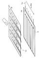
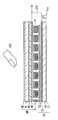
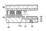
図4は、本実施の形態のタッチセンサ付き表示装置の要部断面構造を表すものである。このタッチセンサ付き表示装置は、表示素子として液晶表示素子を用いると共に、この液晶表示素子に元々備えられている電極の一部(後述する共通電極43)および表示用駆動信号(後述するコモン駆動信号Vcom)を兼用して静電容量型タッチセンサを構成したものである。 First Embodiment
FIG. 4 shows the cross-sectional structure of the main part of the display device with a touch sensor according to the present embodiment. The display device with a touch sensor uses a liquid crystal display element as a display element, and also a part of the electrodes originally provided in the liquid crystal display element (
次に、第2の実施の形態について説明する。本実施の形態は、上記第1の実施の形態の場合とは異なり、表示素子として横電界モードの液晶素子を用いるようにしたものである。 Second Embodiment
Next, a second embodiment will be described. This embodiment differs from the first embodiment in that a liquid crystal element in a transverse electric field mode is used as a display element.
第2の実施の形態では、センサ用検出電極44をガラス基板41の表面側(液晶層6と反対側)に設けるようにしたが、次のような変形が可能である。 [Modification]
In the second embodiment, the
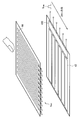
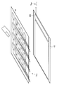
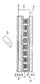
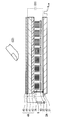
上記第1および第2の実施の形態では、センサ用検出電極44を表示領域に配設するようにしたが、本実施の形態は、図16,図17に示したように、センサ用検出電極44を表示領域Dの周りの領域(額縁領域F)に設けるようにしたものである。なお、図17は本実施の形態のタッチセンサ付き表示装置の平面構成を表し、図16は、図17におけるA-A矢視断面を表す。 Third Embodiment
In the first and second embodiments, the
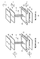
上記第3の実施の形態では、TFT基板21上に共通電極43とセンサ用検出電極44とを並べて配設し、横方向容量結合により容量素子C1を形成するようにしたが、これとは異なり、縦方向容量結合により容量素子C1を形成することも可能である。例えば図19に示したように、共通電極43をTFT基板21上の表示領域Dのみならず額縁領域Fにまで延在させると共に、センサ用検出電極44を、TFT基板21の額縁領域Fにおいて、共通電極43と異なる階層の電極層として共通電極43に対向するように形成する。これにより、共通電極43とセンサ用検出電極44との間に容量素子C1が形成される。この場合には、センサ用検出電極44とTFT基板21との間を結ぶコンタクト導電柱7Cを設け、これにより、センサ用検出電極44からの検出信号VdetをTFT基板21側に伝送するようにすればよい。 [Modification]
In the third embodiment, the
Claims (23)
- 複数の表示画素電極と、
前記表示画素電極と対向して設けられた共通電極と、
画像表示機能を有する表示機能層と、
画像信号に基づいて、前記表示画素電極と前記共通電極との間に表示用電圧を印加して前記表示機能層の表示機能を発揮させるように画像表示制御を行う表示制御回路と、
前記共通電極と対向して、または並んで設けられ、前記共通電極との間に静電容量を形成するタッチ検出電極と
を備えたタッチセンサ付き表示装置。 With multiple display pixel electrodes,
A common electrode provided opposite to the display pixel electrode;
A display function layer having an image display function,
A display control circuit performing image display control so as to exert a display function of the display functional layer by applying a display voltage between the display pixel electrode and the common electrode based on an image signal;
A touch sensor-equipped display device comprising: a touch detection electrode which is provided opposite to or in line with the common electrode and which forms a capacitance with the common electrode. - 前記表示制御部により前記共通電極に印加される表示用駆動電圧をタッチセンサ用駆動信号として利用し、前記タッチ検出電極から得られる検出信号に基づき、物体の接触位置を検出するタッチ検出回路
をさらに備えた請求項1に記載のタッチセンサ付き表示装置。 The touch detection circuit further detects a touch position of an object based on a detection signal obtained from the touch detection electrode, using the display drive voltage applied to the common electrode by the display control unit as a touch sensor drive signal. The display device with a touch sensor according to claim 1 provided. - 前記表示制御回路が形成された回路基板と、
この回路基板と対向して配設された対向基板と
を備え、
前記表示画素電極が、前記回路基板の、前記対向基板に近い側に配設され、
前記共通電極が、前記対向基板の、前記回路基板に近い側に配設され、
前記回路基板の前記表示画素電極と、前記対向基板の前記共通電極との間に、前記表示機能層が挿設されている
請求項2に記載のタッチセンサ付き表示装置。 A circuit board on which the display control circuit is formed;
And an opposing substrate disposed opposite to the circuit substrate,
The display pixel electrode is disposed on a side of the circuit substrate closer to the counter substrate;
The common electrode is disposed on the side closer to the circuit board of the counter substrate,
The display device with a touch sensor according to claim 2, wherein the display functional layer is inserted between the display pixel electrode of the circuit board and the common electrode of the counter substrate. - 前記タッチ検出電極が、前記対向基板の、前記回路基板とは反対側に配設されている
請求項3に記載のタッチセンサ付き表示装置。 The display device with a touch sensor according to claim 3, wherein the touch detection electrode is disposed on the side opposite to the circuit board on the counter substrate. - 前記タッチ検出電極が複数の電極パターンに分割されている
請求項3に記載のタッチセンサ付き表示装置。 The display device with a touch sensor according to claim 3, wherein the touch detection electrode is divided into a plurality of electrode patterns. - 前記タッチ検出回路が、前記回路基板に形成されている
請求項3に記載のタッチセンサ付き表示装置。 The display device with a touch sensor according to claim 3, wherein the touch detection circuit is formed on the circuit board. - 前記表示機能層が液晶層である
請求項3に記載のタッチセンサ付き表示装置。 The display device with a touch sensor according to claim 3, wherein the display function layer is a liquid crystal layer. - 前記表示制御回路が形成された回路基板と、
この回路基板と対向して配設された対向基板と
を備え、
前記回路基板に前記共通電極および前記表示画素電極が絶縁層を介して順に積層され、
前記回路基板の前記表示画素電極と、前記対向基板との間に前記表示機能層が挿設されている
請求項2に記載のタッチセンサ付き表示装置。 A circuit board on which the display control circuit is formed;
And an opposing substrate disposed opposite to the circuit substrate,
The common electrode and the display pixel electrode are sequentially stacked on the circuit substrate via an insulating layer;
The display device with a touch sensor according to claim 2, wherein the display functional layer is inserted between the display pixel electrode of the circuit board and the counter substrate. - 前記タッチ検出電極が前記回路基板に配設されている
請求項8に記載のタッチセンサ付き表示装置。 The display device with a touch sensor according to claim 8, wherein the touch detection electrode is disposed on the circuit board. - 前記共通電極が、前記回路基板の表示領域の内側に配設され、
前記タッチ検出電極が、前記回路基板上の前記表示領域を取り囲む額縁領域に、前記共通電極と同一階層の電極層として前記共通電極から隔てて形成されている
請求項9に記載のタッチセンサ付き表示装置。 The common electrode is disposed inside a display area of the circuit board;
10. The display with a touch sensor according to claim 9, wherein the touch detection electrode is formed in a frame area surrounding the display area on the circuit substrate as an electrode layer in the same layer as the common electrode and separated from the common electrode. apparatus. - 前記共通電極が、前記回路基板上の前記表示領域から前記額縁領域にまで延在し、
前記タッチ検出電極が、前記回路基板の前記額縁領域において、前記共通電極と異なる階層の電極層として前記共通電極に対向して形成されている
請求項9に記載のタッチセンサ付き表示装置。 The common electrode extends from the display area on the circuit board to the frame area;
The display device with a touch sensor according to claim 9, wherein the touch detection electrode is formed to face the common electrode as an electrode layer of a layer different from the common electrode in the frame area of the circuit substrate. - 前記タッチ検出電極を電磁的にシールドするシールド電極が配設されている
請求項9に記載のタッチセンサ付き表示装置。 The display device with a touch sensor according to claim 9, further comprising: a shield electrode that electromagnetically shields the touch detection electrode. - 前記タッチ検出電極が前記対向基板に配設されている
請求項8に記載のタッチセンサ付き表示装置。 The display device with a touch sensor according to claim 8, wherein the touch detection electrode is disposed on the counter substrate. - 前記タッチ検出電極が、前記対向基板の、前記回路基板に近い側に配設されている
請求項13に記載のタッチセンサ付き表示装置。 The display device with a touch sensor according to claim 13, wherein the touch detection electrode is disposed on a side closer to the circuit board of the counter substrate. - 前記タッチ検出電極が、前記対向基板の、前記回路基板とは反対側に配設されている
請求項13に記載のタッチセンサ付き表示装置。 The display device with a touch sensor according to claim 13, wherein the touch detection electrode is disposed on the opposite side of the counter substrate to the circuit board. - 前記タッチ検出電極が、薄膜プロセスにより前記対向基板の上に直接形成されている
請求項15に記載のタッチセンサ付き表示装置。 The display device with a touch sensor according to claim 15, wherein the touch detection electrode is directly formed on the counter substrate by a thin film process. - 前記タッチ検出電極がフィルム基体上に形成され、このタッチ検出電極の形成されたフィルム基体が前記対向基板に貼り付けられている
請求項15に記載のタッチセンサ付き表示装置。 The display device with a touch sensor according to claim 15, wherein the touch detection electrode is formed on a film base, and the film base on which the touch detection electrode is formed is attached to the counter substrate. - 前記タッチ検出回路が、前記回路基板に形成されている
請求項13に記載のタッチセンサ付き表示装置。 The display device with a touch sensor according to claim 13, wherein the touch detection circuit is formed on the circuit board. - 前記対向基板の前記タッチ検出電極と前記回路基板の前記タッチ検出回路との間を接続する導電経路が形成されている
請求項18に記載のタッチセンサ付き表示装置。 The display device with a touch sensor according to claim 18, wherein a conductive path is formed to connect between the touch detection electrode of the opposing substrate and the touch detection circuit of the circuit board. - 前記対向基板の前記タッチ検出電極と前記回路基板の前記タッチ検出回路との間を容量結合する容量結合経路が形成されている
請求項18に記載のタッチセンサ付き表示装置。 The display device with a touch sensor according to claim 18, further comprising: a capacitive coupling path that capacitively couples between the touch detection electrode of the counter substrate and the touch detection circuit of the circuit board. - 前記対向基板の前記タッチ検出電極が高抵抗を介して接地されている
請求項20に記載のタッチセンサ付き表示装置。 The display device with a touch sensor according to claim 20, wherein the touch detection electrode of the counter substrate is grounded via a high resistance. - 前記タッチ検出電極が複数の電極パターンに分割されている
請求項8に記載のタッチセンサ付き表示装置。 The display device with a touch sensor according to claim 8, wherein the touch detection electrode is divided into a plurality of electrode patterns. - 前記表示機能層が液晶層であり、横電界モードでの液晶表示が行われる
請求項8に記載のタッチセンサ付き表示装置。 The display device with a touch sensor according to claim 8, wherein the display function layer is a liquid crystal layer, and liquid crystal display is performed in a transverse electric field mode.
Priority Applications (9)
| Application Number | Priority Date | Filing Date | Title |
|---|---|---|---|
| CN200980000383.XA CN101681221B (en) | 2008-03-28 | 2009-03-25 | Display device provided with touch sensor |
| US12/601,310 US8786557B2 (en) | 2008-03-28 | 2009-03-25 | Display device with touch sensor |
| US14/168,871 US9335875B2 (en) | 2008-03-28 | 2014-01-30 | Display device with touch sensor |
| US14/302,481 US9542047B2 (en) | 2008-03-28 | 2014-06-12 | Display device with touch sensor |
| US15/226,192 US10037116B2 (en) | 2008-03-28 | 2016-08-02 | Display device with touch sensor |
| US16/016,055 US10768755B2 (en) | 2008-03-28 | 2018-06-22 | Display device with touch sensor |
| US16/927,599 US11402682B2 (en) | 2008-03-28 | 2020-07-13 | Touch sensor device |
| US17/847,428 US11686964B2 (en) | 2008-03-28 | 2022-06-23 | Touch sensor device |
| US18/315,566 US20230280610A1 (en) | 2008-03-28 | 2023-05-11 | Touch sensor device |
Applications Claiming Priority (2)
| Application Number | Priority Date | Filing Date | Title |
|---|---|---|---|
| JP2008087739A JP4816668B2 (en) | 2008-03-28 | 2008-03-28 | Display device with touch sensor |
| JP2008-087739 | 2008-03-28 |
Related Child Applications (3)
| Application Number | Title | Priority Date | Filing Date |
|---|---|---|---|
| US12/601,310 A-371-Of-International US8786557B2 (en) | 2008-03-28 | 2009-03-25 | Display device with touch sensor |
| US14/168,871 Continuation US9335875B2 (en) | 2008-03-28 | 2014-01-30 | Display device with touch sensor |
| US14/302,481 Continuation US9542047B2 (en) | 2008-03-28 | 2014-06-12 | Display device with touch sensor |
Publications (1)
| Publication Number | Publication Date |
|---|---|
| WO2009119664A1 true WO2009119664A1 (en) | 2009-10-01 |
Family
ID=41113855
Family Applications (1)
| Application Number | Title | Priority Date | Filing Date |
|---|---|---|---|
| PCT/JP2009/055949 WO2009119664A1 (en) | 2008-03-28 | 2009-03-25 | Display device provided with touch sensor |
Country Status (6)
| Country | Link |
|---|---|
| US (8) | US8786557B2 (en) |
| JP (1) | JP4816668B2 (en) |
| KR (1) | KR101599072B1 (en) |
| CN (1) | CN101681221B (en) |
| TW (1) | TWI406047B (en) |
| WO (1) | WO2009119664A1 (en) |
Cited By (31)
| Publication number | Priority date | Publication date | Assignee | Title |
|---|---|---|---|---|
| JP2011081766A (en) * | 2009-10-06 | 2011-04-21 | Samsung Mobile Display Co Ltd | Liquid crystal display device with built-in touch screen |
| CN102043184A (en) * | 2009-10-09 | 2011-05-04 | Lg化学株式会社 | Integrated touch polarizer and touch panel comprising the same |
| WO2011095102A1 (en) * | 2010-02-04 | 2011-08-11 | 深圳市汇顶科技有限公司 | Capacitive type touch sensor, touch detection device and touch control terminal |
| US20120075240A1 (en) * | 2010-09-29 | 2012-03-29 | Sony Corporation | Display unit with touch detection function and electronic unit |
| JP2012098687A (en) * | 2010-10-29 | 2012-05-24 | Samsung Mobile Display Co Ltd | Touch screen panel incorporated liquid crystal display device |
| JP2012103658A (en) * | 2010-11-08 | 2012-05-31 | Samsung Mobile Display Co Ltd | Touch screen panel integrated liquid crystal display device |
| JP2012113520A (en) * | 2010-11-25 | 2012-06-14 | Hitachi Displays Ltd | Display device |
| KR101188254B1 (en) * | 2010-01-21 | 2012-10-09 | 티피케이 터치 솔루션스 인코포레이션 | Embedded touch sensitive display and a method of manufacturing the same |
| JP2013020611A (en) * | 2011-07-12 | 2013-01-31 | Trendon Touch Technology Corp | Touch sensing circuit and touch point detecting method |
| CN103163676A (en) * | 2012-09-26 | 2013-06-19 | 敦泰科技有限公司 | Liquid crystal display touch screen integrating single layer capacitance transducer and application device thereof |
| US8570300B2 (en) * | 2010-09-24 | 2013-10-29 | Japan Display West, Inc. | Touch detection function display device and electronic apparatus |
| US8847917B2 (en) | 2009-10-06 | 2014-09-30 | Samsung Display Co., Ltd. | Liquid crystal display having a built-in touch screen using capacitance and sense lines for detecting a touch position |
| WO2015125864A1 (en) * | 2014-02-20 | 2015-08-27 | シャープ株式会社 | Touch panel |
| EP2539798A4 (en) * | 2010-02-26 | 2016-03-30 | Synaptics Inc | Varying demodulation to avoid interference |
| JP2016110112A (en) * | 2014-12-02 | 2016-06-20 | 株式会社半導体エネルギー研究所 | Semiconductor device, and display device |
| WO2017057097A1 (en) * | 2015-09-30 | 2017-04-06 | 日東電工株式会社 | In-cell liquid crystal panel and liquid crystal display device |
| JP2017068025A (en) * | 2015-09-30 | 2017-04-06 | 日東電工株式会社 | In-cell liquid crystal panel and liquid crystal display |
| JP2017068026A (en) * | 2015-09-30 | 2017-04-06 | 日東電工株式会社 | In-cell liquid crystal panel and liquid crystal display |
| US10067621B2 (en) | 2015-03-27 | 2018-09-04 | Semiconductor Energy Laboratory Co., Ltd. | Touch panel |
| JP2018141990A (en) * | 2018-04-03 | 2018-09-13 | 日東電工株式会社 | Liquid crystal panel with touch sensing function and liquid crystal display |
| WO2018181490A1 (en) * | 2017-03-28 | 2018-10-04 | 日東電工株式会社 | Polarizing film with added adhesive layer, polarizing film with added adhesive layer for in-cell liquid crystal panel, in-cell liquid crystal panel, and liquid crystal display device |
| WO2018181495A1 (en) * | 2017-03-28 | 2018-10-04 | 日東電工株式会社 | Polarizing film with added adhesive layer, polarizing film with added adhesive layer for in-cell liquid crystal panel, in-cell liquid crystal panel, and liquid crystal display device |
| WO2018181414A1 (en) * | 2017-03-28 | 2018-10-04 | 日東電工株式会社 | Polarizing film with added adhesive layer, polarizing film with added adhesive layer for in-cell liquid crystal panel, in-cell liquid crystal panel, and liquid crystal display device |
| WO2018181416A1 (en) * | 2017-03-28 | 2018-10-04 | 日東電工株式会社 | Polarizing film with added adhesive layer, polarizing film with added adhesive layer for in-cell liquid crystal panel, in-cell liquid crystal panel, and liquid crystal display device |
| WO2018181415A1 (en) * | 2017-03-28 | 2018-10-04 | 日東電工株式会社 | Polarizing film with added adhesive layer, polarizing film with added adhesive layer for in-cell liquid crystal panel, in-cell liquid crystal panel, and liquid crystal display device |
| DE102011005147B4 (en) | 2010-03-19 | 2019-05-02 | Lg Display Co., Ltd. | A touch-sensitive liquid crystal display device and method of manufacturing the same |
| JPWO2018181477A1 (en) * | 2017-03-28 | 2019-06-27 | 日東電工株式会社 | In-cell type liquid crystal panel and liquid crystal display device |
| WO2020111236A1 (en) * | 2018-11-29 | 2020-06-04 | 日東電工株式会社 | Liquid crystal panel with touch sensing function, liquid crystal display device, and polarizing film with adhesive layer |
| JP2020095262A (en) * | 2018-11-29 | 2020-06-18 | 日東電工株式会社 | Liquid crystal panel with touch sensing capability, liquid crystal display device, and polarizing film with adhesive layer |
| JP2021006919A (en) * | 2015-05-29 | 2021-01-21 | 株式会社半導体エネルギー研究所 | Semiconductor device |
| US11256129B2 (en) | 2017-03-28 | 2022-02-22 | Nitto Denko Corporation | In-cell liquid crystal panel and liquid crystal display device |
Families Citing this family (334)
| Publication number | Priority date | Publication date | Assignee | Title |
|---|---|---|---|---|
| US7663607B2 (en) | 2004-05-06 | 2010-02-16 | Apple Inc. | Multipoint touchscreen |
| CN104965621B (en) | 2006-06-09 | 2018-06-12 | 苹果公司 | Touch screen LCD and its operating method |
| US8654083B2 (en) | 2006-06-09 | 2014-02-18 | Apple Inc. | Touch screen liquid crystal display |
| US9710095B2 (en) | 2007-01-05 | 2017-07-18 | Apple Inc. | Touch screen stack-ups |
| JP4816668B2 (en) * | 2008-03-28 | 2011-11-16 | ソニー株式会社 | Display device with touch sensor |
| TW200942459A (en) * | 2008-04-07 | 2009-10-16 | rui-yang Zhang | Auto-inflatable capsule |
| JP5481040B2 (en) * | 2008-04-11 | 2014-04-23 | 株式会社ジャパンディスプレイ | Display device and driving method thereof |
| JP5206250B2 (en) * | 2008-05-02 | 2013-06-12 | セイコーエプソン株式会社 | Display device and electronic device |
| KR101350573B1 (en) * | 2008-12-30 | 2014-01-10 | 엘지디스플레이 주식회사 | Electrophoresis display device |
| US8643624B2 (en) * | 2009-03-18 | 2014-02-04 | Synaptics Incorporated | Capacitive sensing using a segmented common voltage electrode of a display |
| JP5366051B2 (en) * | 2009-04-20 | 2013-12-11 | 株式会社ジャパンディスプレイ | Information input device, display device |
| TWI431362B (en) * | 2009-05-29 | 2014-03-21 | Japan Display West Inc | Touch sensor, display and electronic device |
| US8456586B2 (en) | 2009-06-11 | 2013-06-04 | Apple Inc. | Portable computer display structures |
| JP5439114B2 (en) * | 2009-10-21 | 2014-03-12 | 株式会社ジャパンディスプレイ | Capacitance type input device and electro-optical device with input device |
| US8408780B2 (en) | 2009-11-03 | 2013-04-02 | Apple Inc. | Portable computer housing with integral display |
| US8743309B2 (en) | 2009-11-10 | 2014-06-03 | Apple Inc. | Methods for fabricating display structures |
| CN102096489B (en) * | 2009-12-11 | 2013-04-03 | 胜华科技股份有限公司 | Touch display panel |
| EP2542954B1 (en) | 2010-02-10 | 2017-11-01 | Microchip Technology Germany GmbH | System and method for the generation of a signal correlated with a manual input operation |
| TWI420117B (en) * | 2010-02-11 | 2013-12-21 | Novatek Microelectronics Corp | Capacitance sensing apparatus and touch sensing system |
| KR101633601B1 (en) * | 2010-03-04 | 2016-06-27 | 엘지디스플레이 주식회사 | Liquid crystal display panel with a built-in touch screen, and liquid crystal display device having the same |
| KR101307962B1 (en) | 2010-03-19 | 2013-09-12 | 엘지디스플레이 주식회사 | In-plane switching mode liquid crystal display device having touch sensing function and method of fabricating the same |
| JPWO2011122352A1 (en) * | 2010-03-29 | 2013-07-08 | シャープ株式会社 | Display device, pressure detection device, and display device manufacturing method |
| TWI435140B (en) * | 2010-04-09 | 2014-04-21 | Wintek Corp | Display with touch panel |
| US8941395B2 (en) | 2010-04-27 | 2015-01-27 | 3M Innovative Properties Company | Integrated passive circuit elements for sensing devices |
| JP2011233019A (en) | 2010-04-28 | 2011-11-17 | Sony Corp | Display device with touch detection function, drive circuit, drive system, and electronic equipment |
| JP5455126B2 (en) | 2010-04-28 | 2014-03-26 | 株式会社ジャパンディスプレイ | Display device with touch detection function, driving method, and electronic device |
| JP5523191B2 (en) * | 2010-04-30 | 2014-06-18 | 株式会社ジャパンディスプレイ | Display device with touch detection function |
| US9898121B2 (en) | 2010-04-30 | 2018-02-20 | Synaptics Incorporated | Integrated capacitive sensing and displaying |
| CN101825796B (en) * | 2010-05-19 | 2012-06-13 | 北京富纳特创新科技有限公司 | Touch liquid crystal screen |
| KR101274649B1 (en) * | 2010-05-27 | 2013-06-12 | 엘지디스플레이 주식회사 | Liquid Crystal Display Device including Touch Panel and Method for Manufacturing the Same |
| JP5237330B2 (en) * | 2010-06-15 | 2013-07-17 | 信越ポリマー株式会社 | Sensor sheet and input device |
| KR101735386B1 (en) * | 2010-06-25 | 2017-05-30 | 엘지디스플레이 주식회사 | Liquid crystal display device having touch sensor embedded therein, method for driving the same and method for fabricating the same |
| KR20120010795A (en) * | 2010-07-27 | 2012-02-06 | 삼성전기주식회사 | Electronic paper associated with touch panel |
| JP5513308B2 (en) * | 2010-08-19 | 2014-06-04 | 株式会社ジャパンディスプレイ | Display device with touch detection function and electronic device |
| KR20120017587A (en) * | 2010-08-19 | 2012-02-29 | 삼성모바일디스플레이주식회사 | Liquid crystal display integrated touch screen panel |
| JP5722573B2 (en) | 2010-08-24 | 2015-05-20 | 株式会社ジャパンディスプレイ | Display device with touch detection function |
| JP5653686B2 (en) * | 2010-08-24 | 2015-01-14 | 株式会社ジャパンディスプレイ | Display device with touch detection function |
| WO2012030183A2 (en) * | 2010-09-01 | 2012-03-08 | Lee Sung Ho | Capacitive touch detection apparatus using level shift, detection method using level shift, and display device having the detection apparatus built therein |
| KR101733140B1 (en) | 2010-09-14 | 2017-05-08 | 삼성디스플레이 주식회사 | Display Device Integrated Touch Screen Panel and Fabricating Method Thereof |
| JP5458443B2 (en) * | 2010-09-14 | 2014-04-02 | 株式会社ジャパンディスプレイ | Display device with touch detection function and electronic device |
| JP5667824B2 (en) | 2010-09-24 | 2015-02-12 | 株式会社ジャパンディスプレイ | Touch detection device and driving method thereof, display device with touch detection function, and electronic device |
| JP5616184B2 (en) | 2010-09-28 | 2014-10-29 | 株式会社ジャパンディスプレイ | Display device with touch detection function and electronic device |
| KR101188983B1 (en) | 2010-09-30 | 2012-10-08 | 삼성디스플레이 주식회사 | 3 Dimension Plat Panel Display having a Touch Screen Panel |
| KR101790977B1 (en) * | 2010-10-08 | 2017-10-26 | 엘지디스플레이 주식회사 | Liquid crystal display device |
| KR101897969B1 (en) * | 2010-10-12 | 2018-09-12 | 엘지디스플레이 주식회사 | Liquid crystal display device |
| US9143668B2 (en) | 2010-10-29 | 2015-09-22 | Apple Inc. | Camera lens structures and display structures for electronic devices |
| US8467177B2 (en) | 2010-10-29 | 2013-06-18 | Apple Inc. | Displays with polarizer windows and opaque masking layers for electronic devices |
| CN102455536B (en) * | 2010-10-29 | 2014-11-19 | 三星显示有限公司 | Liquid crystal display integrated touch screen panel and driving method thereof |
| KR20120045290A (en) * | 2010-10-29 | 2012-05-09 | 삼성모바일디스플레이주식회사 | Liquid crystal display integrated touch screen panel |
| KR101230146B1 (en) | 2010-10-29 | 2013-02-05 | 삼성디스플레이 주식회사 | Liquid Crystal Display integrated Touch Screen Panel and Driving Method thereof |
| KR101755601B1 (en) | 2010-11-04 | 2017-07-10 | 삼성디스플레이 주식회사 | Liquid Crystal Display integrated Touch Screen Panel |
| WO2012063787A1 (en) * | 2010-11-10 | 2012-05-18 | シャープ株式会社 | Display device |
| KR101770319B1 (en) | 2010-11-25 | 2017-08-22 | 엘지디스플레이 주식회사 | Liquid crystal display device |
| CN102479011B (en) * | 2010-11-29 | 2015-07-22 | 北京京东方光电科技有限公司 | Capacitive touch screen |
| US8804056B2 (en) | 2010-12-22 | 2014-08-12 | Apple Inc. | Integrated touch screens |
| KR20120072864A (en) * | 2010-12-24 | 2012-07-04 | 삼성전자주식회사 | Display apparatus |
| CN102541330B (en) * | 2010-12-27 | 2015-04-29 | 上海天马微电子有限公司 | Touch control screen and touch control display device |
| CN102156565B (en) * | 2010-12-31 | 2014-11-05 | 深圳超多维光电子有限公司 | Display equipment and method, and naked eye three-dimensional display device |
| TWI471796B (en) * | 2011-02-11 | 2015-02-01 | Wintek Corp | Touch-sensitive display device |
| JP5927532B2 (en) | 2011-03-22 | 2016-06-01 | 株式会社Joled | Display device and electronic device |
| CN102736287B (en) * | 2011-03-29 | 2015-08-12 | 瀚宇彩晶股份有限公司 | Touch control display apparatus |
| JP5789113B2 (en) | 2011-03-31 | 2015-10-07 | 株式会社Joled | Display device and electronic device |
| KR101819677B1 (en) * | 2011-04-01 | 2018-01-17 | 엘지디스플레이 주식회사 | Touch sensor integrated type display device |
| JP5788766B2 (en) * | 2011-11-04 | 2015-10-07 | 株式会社ジャパンディスプレイ | Display panel with touch detection function, driving method thereof, driving circuit, and electronic device |
| JP5726606B2 (en) | 2011-04-13 | 2015-06-03 | 株式会社ジャパンディスプレイ | Display panel with touch detection function, driving method thereof, driving circuit, and electronic device |
| US8791916B2 (en) | 2011-04-13 | 2014-07-29 | Japan Display West, Inc. | Display panel with touch detection function, method of driving the same, driving circuit, and electronic unit |
| JP5710449B2 (en) * | 2011-04-13 | 2015-04-30 | 株式会社ジャパンディスプレイ | Display device, driving circuit, driving method, and electronic apparatus |
| US9141247B2 (en) | 2011-04-13 | 2015-09-22 | Japan Display Inc. | Display panel with touch detection function, method of driving the same, driving circuit, and electronic unit |
| JP5685132B2 (en) * | 2011-04-13 | 2015-03-18 | 株式会社ジャパンディスプレイ | Display panel with touch detection function, drive circuit, and electronic device |
| JP2013012182A (en) * | 2011-05-27 | 2013-01-17 | Kyocera Corp | Input unit, display unit, and electronic device |
| JP2012248743A (en) * | 2011-05-30 | 2012-12-13 | Japan Display West Co Ltd | Semiconductor device, manufacturing method of the semiconductor device, display device, and electronic apparatus |
| CN102650775B (en) * | 2011-06-03 | 2015-09-30 | 北京京东方光电科技有限公司 | Color membrane substrates and manufacture method, touch controlled type display panels |
| JP5811638B2 (en) * | 2011-07-01 | 2015-11-11 | 凸版印刷株式会社 | Color filter with wiring for touch panel |
| US8970545B2 (en) | 2011-07-13 | 2015-03-03 | Synaptics Incorporated | Trace shielding for input devices |
| JP2013029949A (en) * | 2011-07-28 | 2013-02-07 | Japan Display East Co Ltd | Touch panel and touch panel built-in display device |
| WO2013018495A1 (en) * | 2011-07-29 | 2013-02-07 | シャープ株式会社 | Touch panel substrate and display panel |
| US9470941B2 (en) | 2011-08-19 | 2016-10-18 | Apple Inc. | In-cell or on-cell touch sensor with color filter on array |
| US8907921B2 (en) | 2011-08-30 | 2014-12-09 | Synaptics Incorporated | Interference sensing within a display device with an integrated sensing device |
| CN105022540B (en) | 2011-09-07 | 2018-11-09 | 辛纳普蒂克斯公司 | Capacitive sensing during non-display renewal time |
| JP5685512B2 (en) * | 2011-09-29 | 2015-03-18 | 株式会社ジャパンディスプレイ | Display device, touch detection device, driving method, and electronic device |
| WO2013048195A2 (en) | 2011-09-29 | 2013-04-04 | Lee Sung Ho | Touch detection means, detection method, and touch screen panel using driving back phenomenon, and display device having touch screen panel embedded therein |
| TWI461999B (en) * | 2011-10-06 | 2014-11-21 | Mstar Semiconductor Inc | Mutual-capacitance touch sensing device and mutual-capacitance touch sensing electronic system including the same |
| JP5734805B2 (en) | 2011-10-12 | 2015-06-17 | 株式会社ジャパンディスプレイ | Display device, driving circuit, driving method, and electronic apparatus |
| US9298304B2 (en) | 2011-10-12 | 2016-03-29 | Htc Corporation | Electronic device and touch-sensing method |
| JP5667960B2 (en) * | 2011-10-14 | 2015-02-12 | 株式会社ジャパンディスプレイ | Display device, touch detection device, and electronic device |
| JP5628774B2 (en) | 2011-11-07 | 2014-11-19 | 株式会社ジャパンディスプレイ | Display device with touch sensor, potential control method, and program |
| JP2013101420A (en) * | 2011-11-07 | 2013-05-23 | Japan Display West Co Ltd | Display device and electronic apparatus |
| JP5327408B1 (en) * | 2011-11-11 | 2013-10-30 | パナソニック株式会社 | Touch panel device |
| US9001080B2 (en) * | 2011-11-11 | 2015-04-07 | Panasonic Intellectual Property Management Co., Ltd. | Touch-panel device |
| JP5896692B2 (en) * | 2011-11-16 | 2016-03-30 | 日東電工株式会社 | Input display device |
| JP5635480B2 (en) | 2011-11-22 | 2014-12-03 | 株式会社ジャパンディスプレイ | Display device with touch sensor, potential control method, and program |
| US8922523B2 (en) | 2011-11-29 | 2014-12-30 | Apple Inc. | Embedded force measurement |
| TWI456262B (en) * | 2011-12-16 | 2014-10-11 | Wintek Corp | Switchable touch stereoscopic image device |
| WO2013096860A1 (en) * | 2011-12-22 | 2013-06-27 | Bo Pi | A capacitive touch sensor partially integrated with lcd display |
| KR101524449B1 (en) * | 2011-12-22 | 2015-06-02 | 엘지디스플레이 주식회사 | Liquid crystal display device and Method for manufacturing the same |
| CN107256104B (en) | 2012-01-12 | 2020-03-20 | 辛纳普蒂克斯公司 | Single-layer capacitive image sensor |
| JP6022164B2 (en) * | 2012-01-24 | 2016-11-09 | 株式会社ジャパンディスプレイ | Liquid crystal display |
| US8970547B2 (en) | 2012-02-01 | 2015-03-03 | Synaptics Incorporated | Noise-adapting touch sensing window |
| CN103246406B (en) * | 2012-02-02 | 2016-08-31 | 群康科技(深圳)有限公司 | Contact panel and comprise the touch control display apparatus of contact panel |
| JP5905730B2 (en) | 2012-02-09 | 2016-04-20 | 株式会社ジャパンディスプレイ | Liquid crystal display with touch panel |
| KR101859515B1 (en) | 2012-02-14 | 2018-05-21 | 삼성디스플레이 주식회사 | Touch panel |
| JP2013168097A (en) | 2012-02-17 | 2013-08-29 | Japan Display West Co Ltd | Display apparatus and display method |
| KR101330320B1 (en) | 2012-02-20 | 2013-11-14 | 엘지디스플레이 주식회사 | Display device with integrated touch screen and method for driving the same |
| JP5726111B2 (en) | 2012-03-14 | 2015-05-27 | 株式会社ジャパンディスプレイ | Image display device |
| KR101466556B1 (en) | 2012-03-29 | 2014-11-28 | 엘지디스플레이 주식회사 | Liquid crystal display device and Method for manufacturing the same |
| KR101380479B1 (en) | 2012-03-30 | 2014-04-01 | 엘지디스플레이 주식회사 | Touch screen integrated display device and method of fabricating the same |
| JP5991709B2 (en) * | 2012-05-01 | 2016-09-14 | 株式会社ジャパンディスプレイ | LCD with built-in touch panel |
| CN102707514B (en) * | 2012-05-03 | 2014-03-26 | 北京京东方光电科技有限公司 | 3D (3-dimensional) touch liquid crystal lens grating, display device and manufacturing methods of 3D touch liquid crystal lens grating and display device |
| CN102692748B (en) * | 2012-05-03 | 2014-03-26 | 北京京东方光电科技有限公司 | Touch control grating, display device and method for realizing 3D and touch control functions |
| TW201346662A (en) * | 2012-05-09 | 2013-11-16 | Wintek Corp | Touch-sensing device and driving method thereof |
| TWI607258B (en) | 2012-05-14 | 2017-12-01 | 友達光電股份有限公司 | Touch display and method for driving a touch display |
| CN103425310A (en) * | 2012-05-22 | 2013-12-04 | 联胜(中国)科技有限公司 | Touch display device and driving method thereof |
| KR101905793B1 (en) | 2012-06-04 | 2018-10-11 | 삼성디스플레이 주식회사 | Organic Light Emitting Display integrated Touch Screen Panel |
| CN103576368A (en) * | 2012-07-23 | 2014-02-12 | 天津富纳源创科技有限公司 | Color filter substrate, touch liquid crystal display panel and device |
| JP6050728B2 (en) * | 2012-07-24 | 2016-12-21 | 株式会社ジャパンディスプレイ | Liquid crystal display device with touch sensor and electronic device |
| KR101902929B1 (en) * | 2012-07-25 | 2018-10-01 | 삼성전자주식회사 | Touch panel, touch screen apparatus and method of driving the same |
| JP6055225B2 (en) | 2012-07-30 | 2016-12-27 | 株式会社ジャパンディスプレイ | Display device with touch panel |
| JP5854947B2 (en) | 2012-08-01 | 2016-02-09 | 株式会社ジャパンディスプレイ | Display device with input device, method for manufacturing the same, and electronic device |
| JP2014032438A (en) | 2012-08-01 | 2014-02-20 | Japan Display Inc | Input device and display device with input device |
| JP5968275B2 (en) | 2012-08-07 | 2016-08-10 | 株式会社ジャパンディスプレイ | Display device with touch sensor and electronic device |
| TW201407249A (en) * | 2012-08-10 | 2014-02-16 | Yan-Hong Du | Active electronic paper touch apparatus |
| US10073568B2 (en) | 2012-08-15 | 2018-09-11 | Synaptics Incorporated | System and method for interference avoidance for a display device comprising an integrated sensing device |
| CN102866815B (en) * | 2012-09-03 | 2015-07-01 | 北京京东方光电科技有限公司 | Capacitance type embedded touch screen and display device |
| US10073550B2 (en) | 2012-09-20 | 2018-09-11 | Synaptics Incorporated | Concurrent input sensing and display updating |
| JP6067302B2 (en) * | 2012-09-28 | 2017-01-25 | シナプティクス・ジャパン合同会社 | Semiconductor device |
| TWI492111B (en) * | 2012-10-02 | 2015-07-11 | 傑聖科技股份有限公司 | Touch panel and manufacturing method |
| CN103713413B (en) * | 2012-10-08 | 2017-01-25 | 群康科技(深圳)有限公司 | Embedded touch display and electronic device |
| TWI495927B (en) * | 2012-10-08 | 2015-08-11 | Innocom Tech Shenzhen Co Ltd | In-cell touch display and electronic apparatus thereof |
| TWI681233B (en) * | 2012-10-12 | 2020-01-01 | 日商半導體能源研究所股份有限公司 | Liquid crystal display device, touch panel and method for manufacturing liquid crystal display device |
| JP6351947B2 (en) | 2012-10-12 | 2018-07-04 | 株式会社半導体エネルギー研究所 | Method for manufacturing liquid crystal display device |
| KR102008779B1 (en) * | 2012-10-22 | 2019-08-09 | 엘지디스플레이 주식회사 | Display Device With Integrated Touch Screen and Method for Driving The Same |
| JP6022320B2 (en) * | 2012-11-20 | 2016-11-09 | 株式会社ジャパンディスプレイ | Liquid crystal display |
| JP6025697B2 (en) | 2012-12-05 | 2016-11-16 | 株式会社ジャパンディスプレイ | Display device with touch detection function, driving method thereof, and electronic device |
| JP6097676B2 (en) | 2012-12-05 | 2017-03-15 | 株式会社ジャパンディスプレイ | Display device with touch detection function and electronic device |
| KR101579353B1 (en) * | 2012-12-05 | 2015-12-21 | 가부시키가이샤 재팬 디스프레이 | Display device with touch detection function and electronic apparutus |
| KR101595626B1 (en) | 2012-12-05 | 2016-02-18 | 가부시키가이샤 재팬 디스프레이 | Display device having touch detection functions, driving method thereof, and electronic apparatus |
| KR101993856B1 (en) * | 2012-12-31 | 2019-06-28 | 삼성디스플레이 주식회사 | Liquid Crystal Display integrated Touch Sensor |
| KR20140095152A (en) * | 2013-01-23 | 2014-08-01 | 삼성디스플레이 주식회사 | Display device |
| JP5909201B2 (en) * | 2013-01-30 | 2016-04-26 | 株式会社ジャパンディスプレイ | Touch detection device, display device with touch detection function and electronic device including the same |
| KR102023436B1 (en) * | 2013-01-30 | 2019-09-20 | 엘지디스플레이 주식회사 | Apparatus for display including touch electrode |
| JP2014153936A (en) | 2013-02-08 | 2014-08-25 | Japan Display Inc | Touch position detection device and touch position detection method |
| US20140232665A1 (en) * | 2013-02-21 | 2014-08-21 | Htc Corporation | Electronic apparatus with a display module integrated with a touch sensor |
| JP2014167514A (en) | 2013-02-28 | 2014-09-11 | Japan Display Central Co Ltd | Liquid crystal display device and driving method of the same |
| JP5508561B2 (en) * | 2013-03-01 | 2014-06-04 | 株式会社ジャパンディスプレイ | Display device |
| JP2014174760A (en) * | 2013-03-08 | 2014-09-22 | Japan Display Inc | Display device attached with touch detection function, and electronic device |
| JP2014174851A (en) | 2013-03-11 | 2014-09-22 | Japan Display Inc | Touch sensor device, display device and electronic device |
| JP2014186409A (en) * | 2013-03-22 | 2014-10-02 | Kyocera Corp | Display device |
| JP2014186537A (en) | 2013-03-22 | 2014-10-02 | Japan Display Inc | Display device, and electronic apparatus |
| KR102141459B1 (en) | 2013-03-22 | 2020-08-05 | 가부시키가이샤 한도오따이 에네루기 켄큐쇼 | Liquid crystal display device |
| JP2014191660A (en) | 2013-03-27 | 2014-10-06 | Japan Display Inc | Display device with touch detection function and electronic apparatus |
| JP5531135B2 (en) * | 2013-03-28 | 2014-06-25 | 信越ポリマー株式会社 | Sensor sheet and input device |
| TWI506773B (en) * | 2013-03-29 | 2015-11-01 | Ye Xin Technology Consulting Co Ltd | Organic electroluminescent type touch display panel |
| JP5866311B2 (en) * | 2013-03-29 | 2016-02-17 | 株式会社ジャパンディスプレイ | Electronic device, electronic device control method |
| JP5914403B2 (en) | 2013-03-29 | 2016-05-11 | 株式会社ジャパンディスプレイ | Display device with touch detection function and electronic device |
| JP5865286B2 (en) | 2013-03-29 | 2016-02-17 | 株式会社ジャパンディスプレイ | Electronic device and control method of electronic device |
| JP5953258B2 (en) | 2013-03-29 | 2016-07-20 | 株式会社ジャパンディスプレイ | Electronic device and control method of electronic device |
| JP5845204B2 (en) | 2013-03-29 | 2016-01-20 | 株式会社ジャパンディスプレイ | Electronic device and control method of electronic device |
| JP5865287B2 (en) | 2013-03-29 | 2016-02-17 | 株式会社ジャパンディスプレイ | Electronic device and control method of electronic device |
| JP5807035B2 (en) | 2013-03-29 | 2015-11-10 | 株式会社ジャパンディスプレイ | Display device with touch detection function, electronic device, and touch detection device |
| JP2014203421A (en) * | 2013-04-10 | 2014-10-27 | 株式会社タッチパネル研究所 | Capacitive touch panel |
| US10416504B2 (en) | 2013-05-21 | 2019-09-17 | Semiconductor Energy Laboratory Co., Ltd. | Liquid crystal display device |
| KR20140139261A (en) | 2013-05-27 | 2014-12-05 | 삼성디스플레이 주식회사 | Display device including touch sensor and driving method thereof |
| CN103294321A (en) * | 2013-06-06 | 2013-09-11 | 敦泰科技有限公司 | Touch control display device |
| CN103279245B (en) * | 2013-06-06 | 2017-03-15 | 敦泰电子有限公司 | Touch control display apparatus |
| TW201447450A (en) | 2013-06-07 | 2014-12-16 | Chunghwa Picture Tubes Ltd | Touch display panel and manufacturing method thereof |
| CN103308817B (en) * | 2013-06-20 | 2015-11-25 | 京东方科技集团股份有限公司 | Array base palte line detection apparatus and detection method |
| JP6121812B2 (en) | 2013-06-25 | 2017-04-26 | 株式会社ジャパンディスプレイ | Liquid crystal display with touch panel |
| JP6131123B2 (en) | 2013-06-25 | 2017-05-17 | 株式会社ジャパンディスプレイ | Display device with touch panel |
| JP2015007924A (en) | 2013-06-25 | 2015-01-15 | 株式会社ジャパンディスプレイ | Liquid crystal display device with touch panel |
| JP6216167B2 (en) | 2013-06-26 | 2017-10-18 | 株式会社ジャパンディスプレイ | Terminal connection structure and display device with built-in touch sensor |
| JP6306295B2 (en) * | 2013-07-09 | 2018-04-04 | 株式会社ジャパンディスプレイ | Display device |
| JP6255179B2 (en) | 2013-07-10 | 2017-12-27 | 株式会社ジャパンディスプレイ | Display device |
| TWI636309B (en) | 2013-07-25 | 2018-09-21 | 日商半導體能源研究所股份有限公司 | Liquid crystal display device and electronic device |
| KR101681305B1 (en) * | 2014-08-01 | 2016-12-02 | 주식회사 하이딥 | Touch input device |
| CN103425347B (en) * | 2013-08-02 | 2018-01-02 | 敦泰电子有限公司 | Touch control display apparatus |
| US9552089B2 (en) | 2013-08-07 | 2017-01-24 | Synaptics Incorporated | Capacitive sensing using a matrix electrode pattern |
| JP2015041235A (en) | 2013-08-21 | 2015-03-02 | 株式会社ジャパンディスプレイ | Liquid crystal display device having touch panel |
| JP6076866B2 (en) * | 2013-09-03 | 2017-02-08 | アルプス電気株式会社 | Capacitance type input device |
| TW201510802A (en) * | 2013-09-14 | 2015-03-16 | Wintek Corp | Touch panel |
| US20150091842A1 (en) | 2013-09-30 | 2015-04-02 | Synaptics Incorporated | Matrix sensor for image touch sensing |
| US10042489B2 (en) | 2013-09-30 | 2018-08-07 | Synaptics Incorporated | Matrix sensor for image touch sensing |
| US9298325B2 (en) | 2013-09-30 | 2016-03-29 | Synaptics Incorporated | Processing system for a capacitive sensing device |
| US9459367B2 (en) | 2013-10-02 | 2016-10-04 | Synaptics Incorporated | Capacitive sensor driving technique that enables hybrid sensing or equalization |
| JP2015072549A (en) | 2013-10-02 | 2015-04-16 | 株式会社ジャパンディスプレイ | Liquid crystal display device with touch panel |
| US9442615B2 (en) | 2013-10-02 | 2016-09-13 | Synaptics Incorporated | Frequency shifting for simultaneous active matrix display update and in-cell capacitive touch |
| JP6165584B2 (en) | 2013-10-08 | 2017-07-19 | 株式会社ジャパンディスプレイ | Display device |
| JP6473581B2 (en) | 2013-10-09 | 2019-02-20 | 株式会社ジャパンディスプレイ | Display device and control method of display device |
| JP6254812B2 (en) * | 2013-10-10 | 2017-12-27 | 株式会社ジャパンディスプレイ | LCD device with built-in touch panel function |
| US9274662B2 (en) | 2013-10-18 | 2016-03-01 | Synaptics Incorporated | Sensor matrix pad for performing multiple capacitive sensing techniques |
| US9864457B2 (en) | 2013-10-22 | 2018-01-09 | Sharp Kabushiki Kaisha | Display device with touch sensor |
| US9495046B2 (en) | 2013-10-23 | 2016-11-15 | Synaptics Incorporated | Parasitic capacitance filter for single-layer capacitive imaging sensors |
| US9081457B2 (en) | 2013-10-30 | 2015-07-14 | Synaptics Incorporated | Single-layer muti-touch capacitive imaging sensor |
| CN109309114B (en) * | 2013-11-12 | 2023-05-26 | 宸鸿光电科技股份有限公司 | Touch display device of organic light emitting diode |
| CN104635967B (en) | 2013-11-12 | 2018-04-10 | 宸鸿光电科技股份有限公司 | Organic Light Emitting Diode touch control display device |
| CN104637977A (en) * | 2013-11-12 | 2015-05-20 | 宸鸿光电科技股份有限公司 | Luminous display device |
| TWI636300B (en) * | 2013-11-15 | 2018-09-21 | 禾瑞亞科技股份有限公司 | Touch display and method for driving a plurality of touch driving electrodes of touch display |
| KR102063349B1 (en) | 2013-11-19 | 2020-01-08 | 엘지디스플레이 주식회사 | Display device and driving method thereof |
| CN104656297B (en) * | 2013-11-19 | 2017-06-13 | 苏州汉朗光电有限公司 | Touch controlled type smectic liquid crystal display |
| CN104678628A (en) * | 2013-11-26 | 2015-06-03 | 瀚宇彩晶股份有限公司 | Embedded touch display panel and drive method thereof |
| KR101712346B1 (en) * | 2014-09-19 | 2017-03-22 | 주식회사 하이딥 | Touch input device |
| KR102261761B1 (en) | 2013-12-12 | 2021-06-07 | 삼성디스플레이 주식회사 | Display device |
| JP6046600B2 (en) * | 2013-12-16 | 2016-12-21 | 株式会社ジャパンディスプレイ | Display device with touch detection function and electronic device |
| TWI609299B (en) * | 2013-12-24 | 2017-12-21 | 鴻海精密工業股份有限公司 | In-cell touch display device |
| JP5687757B2 (en) * | 2013-12-27 | 2015-03-18 | 株式会社ジャパンディスプレイ | Display device with touch detection function, driving method, and electronic device |
| CN103744226B (en) * | 2013-12-30 | 2017-11-03 | 深圳市华星光电技术有限公司 | Touch control display apparatus |
| JP6320227B2 (en) | 2014-01-17 | 2018-05-09 | 株式会社ジャパンディスプレイ | Display device |
| JP6375223B2 (en) * | 2014-01-31 | 2018-08-15 | 株式会社ジャパンディスプレイ | Display device with sensor and driving method thereof |
| JP6326238B2 (en) | 2014-02-06 | 2018-05-16 | 株式会社ジャパンディスプレイ | Display device |
| CN106062619B (en) | 2014-02-28 | 2019-04-16 | 凸版印刷株式会社 | Liquid crystal display device |
| US9798429B2 (en) | 2014-02-28 | 2017-10-24 | Synaptics Incorporated | Guard electrodes in a sensing stack |
| KR101868256B1 (en) | 2014-02-28 | 2018-06-15 | 도판 인사츠 가부시키가이샤 | Lcd device |
| US9582099B2 (en) | 2014-03-31 | 2017-02-28 | Synaptics Incorporated | Serrated input sensing intervals |
| US10133421B2 (en) | 2014-04-02 | 2018-11-20 | Synaptics Incorporated | Display stackups for matrix sensor |
| JP2015200739A (en) * | 2014-04-07 | 2015-11-12 | 株式会社ジャパンディスプレイ | display device |
| CN105022184A (en) * | 2014-04-17 | 2015-11-04 | 株式会社日本显示器 | Display device |
| US9952725B2 (en) * | 2014-04-22 | 2018-04-24 | Semiconductor Energy Laboratory Co., Ltd. | Liquid crystal display device and electronic device having sensor circuit comprising a transistor and a capacitor |
| US20150309636A1 (en) * | 2014-04-25 | 2015-10-29 | Japan Display Inc. | Sensor-equipped display device |
| US9927832B2 (en) | 2014-04-25 | 2018-03-27 | Synaptics Incorporated | Input device having a reduced border region |
| US9298309B2 (en) | 2014-04-29 | 2016-03-29 | Synaptics Incorporated | Source driver touch transmitter in parallel with display drive |
| KR20150131577A (en) * | 2014-05-15 | 2015-11-25 | 엘지전자 주식회사 | Glass Type Terminal |
| US9690397B2 (en) | 2014-05-20 | 2017-06-27 | Synaptics Incorporated | System and method for detecting an active pen with a matrix sensor |
| CN103984442B (en) * | 2014-05-27 | 2017-10-31 | 上海和辉光电有限公司 | Embedded active matrix organic light-emitting diode contact panel |
| CN104020907B (en) * | 2014-05-30 | 2017-02-15 | 京东方科技集团股份有限公司 | In cell touch panel and display device |
| CN104020891A (en) | 2014-05-30 | 2014-09-03 | 京东方科技集团股份有限公司 | In cell touch panel and display device |
| CN104035640B (en) | 2014-05-30 | 2017-10-27 | 京东方科技集团股份有限公司 | A kind of In-cell touch panel and display device |
| JP2015230599A (en) | 2014-06-05 | 2015-12-21 | 株式会社ジャパンディスプレイ | Display device with sensor and its drive method |
| CN106463080B (en) * | 2014-06-13 | 2019-08-20 | 株式会社半导体能源研究所 | Display device |
| US9471173B2 (en) * | 2014-06-30 | 2016-10-18 | Synaptics Incorporated | Capacitive input sensing in the presence of a uniform conductor |
| JP2016024292A (en) | 2014-07-18 | 2016-02-08 | 株式会社ジャパンディスプレイ | Display device with sensor |
| JP5893697B2 (en) * | 2014-09-11 | 2016-03-23 | 株式会社ジャパンディスプレイ | Display device with touch detection function and electronic device |
| JP6310831B2 (en) | 2014-09-26 | 2018-04-11 | 株式会社ジャパンディスプレイ | Display device with sensor and control method of display device |
| CN104391392A (en) * | 2014-09-28 | 2015-03-04 | 京东方科技集团股份有限公司 | 3D (three-dimensional) touch display device as well as production method and drive method thereof |
| CN104281350A (en) * | 2014-09-30 | 2015-01-14 | 京东方科技集团股份有限公司 | Display panel and display device |
| JP6358935B2 (en) | 2014-11-25 | 2018-07-18 | 株式会社ジャパンディスプレイ | Display device and touch detection method |
| JP2016102868A (en) * | 2014-11-27 | 2016-06-02 | 株式会社ジャパンディスプレイ | Display device |
| CN104375732B (en) * | 2014-11-28 | 2018-09-14 | 京东方科技集团股份有限公司 | Embedded touch module, driving method, touch-control display panel and display device |
| US10386964B2 (en) * | 2014-11-28 | 2019-08-20 | Sharp Kabushiki Kaisha | Display device fitted with position input function |
| US10088718B2 (en) | 2014-12-22 | 2018-10-02 | Shanghai Tianma Micro-electronics Co., Ltd. | Touch liquid crystal display and method of controlling the same |
| CN104484085B (en) | 2014-12-22 | 2018-05-25 | 上海天马微电子有限公司 | A kind of capacitive touch screen, its touch localization method and display device |
| US10175827B2 (en) | 2014-12-23 | 2019-01-08 | Synaptics Incorporated | Detecting an active pen using a capacitive sensing device |
| US10394391B2 (en) | 2015-01-05 | 2019-08-27 | Synaptics Incorporated | System and method for reducing display artifacts |
| JP6706621B2 (en) | 2015-01-05 | 2020-06-10 | シナプティクス インコーポレイテッド | Time division of display and sensing data |
| US10990148B2 (en) | 2015-01-05 | 2021-04-27 | Synaptics Incorporated | Central receiver for performing capacitive sensing |
| CN104636015A (en) * | 2015-01-13 | 2015-05-20 | 昆山龙腾光电有限公司 | Touch display device |
| US20160202525A1 (en) * | 2015-01-14 | 2016-07-14 | Japan Display Inc. | Display device |
| JP2016142880A (en) | 2015-01-30 | 2016-08-08 | 株式会社ジャパンディスプレイ | Display device |
| KR102560704B1 (en) * | 2015-02-17 | 2023-07-28 | 삼성디스플레이 주식회사 | Display apparatus and method for manufacturing display apparatus |
| US20180017821A1 (en) * | 2015-02-24 | 2018-01-18 | Sharp Kabushiki Kaisha | Liquid crystal display device with touch sensor |
| JP6395651B2 (en) * | 2015-03-30 | 2018-09-26 | 株式会社ジャパンディスプレイ | Input device and display device |
| JP6489900B2 (en) * | 2015-03-30 | 2019-03-27 | 株式会社ジャパンディスプレイ | Input device and display device |
| CN104698699A (en) * | 2015-04-01 | 2015-06-10 | 上海天马微电子有限公司 | Array substrate, display panel, display device and driving method thereof |
| US9939972B2 (en) | 2015-04-06 | 2018-04-10 | Synaptics Incorporated | Matrix sensor with via routing |
| WO2016163303A1 (en) * | 2015-04-06 | 2016-10-13 | シャープ株式会社 | Liquid-crystal display device with touch sensor |
| US10372274B2 (en) | 2015-04-13 | 2019-08-06 | Semiconductor Energy Laboratory Co., Ltd. | Semiconductor device and touch panel |
| JP2016206790A (en) | 2015-04-17 | 2016-12-08 | 株式会社ジャパンディスプレイ | Touch control method, touch control apparatus, and display device with touch detection function |
| US10002970B2 (en) | 2015-04-30 | 2018-06-19 | Semiconductor Energy Laboratory Co., Ltd. | Semiconductor device, manufacturing method of the same, or display device including the same |
| US10671204B2 (en) | 2015-05-04 | 2020-06-02 | Semiconductor Energy Laboratory Co., Ltd. | Touch panel and data processor |
| US9733756B2 (en) * | 2015-05-12 | 2017-08-15 | Synaptics Incorporated | Integrated display device and sensing device with force sensing |
| TWI611322B (en) * | 2015-05-15 | 2018-01-11 | 瑞鼎科技股份有限公司 | In-cell touch panel |
| KR102619052B1 (en) | 2015-06-15 | 2023-12-29 | 가부시키가이샤 한도오따이 에네루기 켄큐쇼 | Display device |
| JP2017009654A (en) | 2015-06-17 | 2017-01-12 | 株式会社ジャパンディスプレイ | Display device |
| JP6879678B2 (en) * | 2015-06-22 | 2021-06-02 | 株式会社半導体エネルギー研究所 | Semiconductor device |
| JP2015212962A (en) * | 2015-06-24 | 2015-11-26 | 株式会社ジャパンディスプレイ | Display device and electronic apparatus |
| US9715304B2 (en) | 2015-06-30 | 2017-07-25 | Synaptics Incorporated | Regular via pattern for sensor-based input device |
| US9720541B2 (en) | 2015-06-30 | 2017-08-01 | Synaptics Incorporated | Arrangement of sensor pads and display driver pads for input device |
| US10095948B2 (en) | 2015-06-30 | 2018-10-09 | Synaptics Incorporated | Modulation scheme for fingerprint sensing |
| JP6514593B2 (en) | 2015-07-17 | 2019-05-15 | パナソニック液晶ディスプレイ株式会社 | Display unit with touch detection function |
| US10386950B2 (en) | 2015-07-22 | 2019-08-20 | Sharp Kabushiki Kaisha | Touch-panel-equipped display device and method for manufacturing touch-panel-equipped display device |
| CN205028263U (en) | 2015-09-07 | 2016-02-10 | 辛纳普蒂克斯公司 | Capacitance sensor |
| JP6807683B2 (en) | 2015-09-11 | 2021-01-06 | 株式会社半導体エネルギー研究所 | Input / output panel |
| US10591764B2 (en) * | 2015-09-15 | 2020-03-17 | Boe Technology Group Co., Ltd. | Display device having a touch electrode in the peripheral area |
| JP6320358B2 (en) * | 2015-09-29 | 2018-05-09 | 日東電工株式会社 | Liquid crystal panel with touch sensing function and liquid crystal display device |
| US10037112B2 (en) | 2015-09-30 | 2018-07-31 | Synaptics Incorporated | Sensing an active device'S transmission using timing interleaved with display updates |
| CN105259690A (en) * | 2015-10-10 | 2016-01-20 | 武汉华星光电技术有限公司 | Manufacturing method of array substrate, array substrate, and touch control liquid crystal display apparatus |
| CN106610749B (en) | 2015-10-21 | 2019-08-13 | 敦泰电子股份有限公司 | Touch control display apparatus and its driving method |
| CN205334426U (en) | 2015-10-28 | 2016-06-22 | 敦泰电子股份有限公司 | Touch display device |
| JP6603544B2 (en) | 2015-10-28 | 2019-11-06 | 株式会社ジャパンディスプレイ | Touch detection device, display device with touch detection function |
| JP6549976B2 (en) | 2015-11-27 | 2019-07-24 | 株式会社ジャパンディスプレイ | Touch detection device and display device with touch detection function |
| CN105353921B (en) * | 2015-12-08 | 2018-01-23 | 上海天马微电子有限公司 | A kind of integrated touch-control display panel and a kind of touch control display device |
| US10592022B2 (en) | 2015-12-29 | 2020-03-17 | Synaptics Incorporated | Display device with an integrated sensing device having multiple gate driver circuits |
| US10067587B2 (en) * | 2015-12-29 | 2018-09-04 | Synaptics Incorporated | Routing conductors in an integrated display device and sensing device |
| KR102512296B1 (en) | 2015-12-29 | 2023-03-23 | 삼성디스플레이 주식회사 | Display device |
| CN106933400B (en) | 2015-12-31 | 2021-10-29 | 辛纳普蒂克斯公司 | Single layer sensor pattern and sensing method |
| KR20180103107A (en) | 2016-01-20 | 2018-09-18 | 가부시키가이샤 한도오따이 에네루기 켄큐쇼 | Input device, input / output device, and information processing device |
| JP6581927B2 (en) | 2016-03-09 | 2019-09-25 | 株式会社ジャパンディスプレイ | Detection device, display device, and electronic device |
| CN115808825A (en) | 2016-03-15 | 2023-03-17 | 株式会社半导体能源研究所 | Display device, module, and electronic apparatus |
| JP6562862B2 (en) | 2016-03-29 | 2019-08-21 | 株式会社ジャパンディスプレイ | Touch detection device and display device with touch detection function |
| CN105759525A (en) * | 2016-05-13 | 2016-07-13 | 京东方科技集团股份有限公司 | Array substrate, display panel and display device |
| US10416805B2 (en) * | 2016-07-01 | 2019-09-17 | Hannstar Display Corporation | Touch display apparatus |
| KR102365490B1 (en) | 2016-07-13 | 2022-02-18 | 가부시키가이샤 한도오따이 에네루기 켄큐쇼 | Input/output panel, input/output device, and semiconductor device |
| KR101913394B1 (en) * | 2016-07-29 | 2018-10-31 | 삼성디스플레이 주식회사 | Display device |
| TWI656461B (en) * | 2016-07-31 | 2019-04-11 | 矽創電子股份有限公司 | Touch display device |
| CN106444173B (en) * | 2016-08-19 | 2020-03-24 | 京东方科技集团股份有限公司 | Array substrate, display panel and display device |
| TWI607364B (en) | 2016-09-22 | 2017-12-01 | 友達光電股份有限公司 | Touch display panel and driving method thereof |
| JP2018054719A (en) | 2016-09-27 | 2018-04-05 | 株式会社ジャパンディスプレイ | Semiconductor device and display device |
| WO2018061358A1 (en) * | 2016-09-30 | 2018-04-05 | 凸版印刷株式会社 | Light adjustment apparatus |
| CN109791445B (en) | 2016-10-06 | 2023-06-30 | 株式会社和冠 | Touch pen and controller |
| JP6915977B2 (en) * | 2016-10-14 | 2021-08-11 | 株式会社半導体エネルギー研究所 | Display panel, display device, input / output device, information processing device |
| US10345977B2 (en) | 2016-10-14 | 2019-07-09 | Semiconductor Energy Laboratory Co., Ltd. | Input/output panel and semiconductor device having a current sensing circuit |
| US10866449B2 (en) | 2016-11-21 | 2020-12-15 | Sharp Kabushiki Kaisha | Liquid crystal display apparatus with touch sensor and method for driving same |
| CN206193734U (en) | 2016-11-24 | 2017-05-24 | 中华映管股份有限公司 | Touch sensing device |
| JP2018112937A (en) * | 2017-01-12 | 2018-07-19 | 株式会社ジャパンディスプレイ | Display device |
| US10248243B2 (en) * | 2017-01-19 | 2019-04-02 | Hideep Inc. | Touch input device |
| JP6840554B2 (en) * | 2017-01-30 | 2021-03-10 | 株式会社ジャパンディスプレイ | Detection device and display device |
| JP6836415B2 (en) | 2017-02-13 | 2021-03-03 | 株式会社ジャパンディスプレイ | Display device with touch detection function and control device |
| US11353754B2 (en) | 2017-02-21 | 2022-06-07 | Semiconductor Energy Laboratory Co., Ltd. | Display panel, display device, input/output device, and data processing device |
| JP2018147396A (en) | 2017-03-08 | 2018-09-20 | 株式会社ジャパンディスプレイ | Display device |
| JP6366761B2 (en) * | 2017-03-08 | 2018-08-01 | 株式会社ジャパンディスプレイ | Display device with touch detection function |
| JP6849501B2 (en) * | 2017-03-29 | 2021-03-24 | 株式会社ジャパンディスプレイ | Display device |
| JP2018181151A (en) | 2017-04-19 | 2018-11-15 | 株式会社ジャパンディスプレイ | Display apparatus |
| JP6759154B2 (en) | 2017-06-05 | 2020-09-23 | 株式会社ジャパンディスプレイ | Detection device and display device |
| JP2019016154A (en) | 2017-07-06 | 2019-01-31 | 株式会社ジャパンディスプレイ | Display device |
| US10564754B2 (en) | 2017-07-12 | 2020-02-18 | Japan Display Inc. | Display device |
| JP2019067143A (en) | 2017-09-29 | 2019-04-25 | 株式会社ジャパンディスプレイ | Detector and display |
| JP6901949B2 (en) | 2017-09-29 | 2021-07-14 | 株式会社ジャパンディスプレイ | Detection device and display device |
| KR102380866B1 (en) | 2017-09-29 | 2022-03-31 | 엘지디스플레이 주식회사 | Touch display device, touch display panel, and driving circuit |
| US10754481B2 (en) | 2017-11-13 | 2020-08-25 | Japan Display Inc. | Detection device and display device |
| WO2019119146A1 (en) * | 2017-12-22 | 2019-06-27 | 1004335 Ontario Inc. carrying on business as A D Metro | Capacitive touch sensor apparatus having branching electrodes |
| JP7011159B2 (en) * | 2018-01-12 | 2022-01-26 | Tianma Japan株式会社 | Capacitance detection circuit and capacitance sensor device |
| TWI668617B (en) | 2018-08-17 | 2019-08-11 | 友達光電股份有限公司 | Non-rectangular free from touch device |
| CN109101138A (en) * | 2018-08-21 | 2018-12-28 | 武汉华星光电半导体显示技术有限公司 | Array substrate and display panel |
| JP6868069B2 (en) | 2018-09-19 | 2021-05-12 | シャープ株式会社 | Liquid crystal display device with touch sensor using active matrix board and active matrix board |
| JP6804603B2 (en) * | 2018-09-19 | 2020-12-23 | シャープ株式会社 | Manufacturing method of active matrix substrate and manufacturing method of liquid crystal display device with touch sensor using active matrix substrate |
| TWI674464B (en) * | 2018-10-12 | 2019-10-11 | 友達光電股份有限公司 | Array substrate |
| TWI718540B (en) * | 2019-05-23 | 2021-02-11 | 元太科技工業股份有限公司 | Touch structure and manufacturing method thereof and touch display device |
| JP7353903B2 (en) | 2019-10-07 | 2023-10-02 | 株式会社ジャパンディスプレイ | Display device and clock |
| US11637919B2 (en) | 2019-12-03 | 2023-04-25 | Apple Inc. | Handheld electronic device |
| US11522983B2 (en) | 2019-12-03 | 2022-12-06 | Apple Inc. | Handheld electronic device |
| CN111103488A (en) * | 2019-12-25 | 2020-05-05 | 心核心科技(北京)有限公司 | Touch detection circuit, touch sensor and ring receiver |
| JP2021148617A (en) * | 2020-03-19 | 2021-09-27 | 株式会社ジャパンディスプレイ | Display device and watch |
| JP7113061B2 (en) | 2020-12-10 | 2022-08-04 | 株式会社ワコム | Methods and systems performed by a controller for performing stylus sensing operations |
| JP2022110853A (en) * | 2021-01-19 | 2022-07-29 | 株式会社ジャパンディスプレイ | Display device |
| JP7031037B2 (en) * | 2021-03-04 | 2022-03-07 | 株式会社ジャパンディスプレイ | Display device |
| JP2022167632A (en) | 2021-04-23 | 2022-11-04 | シャープディスプレイテクノロジー株式会社 | Active matrix substrate, method for manufacturing active matrix substrate, and liquid crystal display with touch sensor using active matrix substrate |
Citations (4)
| Publication number | Priority date | Publication date | Assignee | Title |
|---|---|---|---|---|
| JP2000148376A (en) * | 1998-11-09 | 2000-05-26 | Toshiba Corp | Data input device |
| WO2006030745A1 (en) * | 2004-09-17 | 2006-03-23 | Sharp Kabushiki Kaisha | Display, viewing angle controller, and electronic apparatus |
| JP2006146895A (en) * | 2004-10-22 | 2006-06-08 | Sharp Corp | Display device with touch sensor, and drive method for the same |
| WO2007102238A1 (en) * | 2006-03-08 | 2007-09-13 | Sharp Kabushiki Kaisha | Display device |
Family Cites Families (43)
| Publication number | Priority date | Publication date | Assignee | Title |
|---|---|---|---|---|
| JPS56135276A (en) | 1980-03-25 | 1981-10-22 | Fujitsu Ltd | Input operating device |
| JPS59216177A (en) | 1983-05-25 | 1984-12-06 | 株式会社日立製作所 | Information holder |
| JPS606925A (en) | 1983-06-24 | 1985-01-14 | Hosiden Electronics Co Ltd | Liquid crystal display element with switch |
| JP3258216B2 (en) | 1995-10-24 | 2002-02-18 | アルプス電気株式会社 | Liquid crystal display with tablet |
| JP3484702B2 (en) * | 1996-03-14 | 2004-01-06 | セイコーエプソン株式会社 | Liquid crystal device and electronic equipment using the same |
| US6751898B2 (en) * | 1996-07-23 | 2004-06-22 | George W. Heropoulos | Electroluminescent display apparatus |
| EP1422601A4 (en) * | 2001-08-22 | 2006-10-18 | Sharp Kk | Touch sensor, display with touch sensor and method for generating position data |
| US7656393B2 (en) * | 2005-03-04 | 2010-02-02 | Apple Inc. | Electronic device having display and surrounding touch sensitive bezel for user interface and control |
| US7358741B2 (en) * | 2004-05-25 | 2008-04-15 | Alps Electric Co., Ltd | Electrostatic detection apparatus and method, and coordinate detection program |
| GB2428306B (en) * | 2005-07-08 | 2007-09-26 | Harald Philipp | Two-dimensional capacitive position sensor |
| US7839392B2 (en) * | 2005-08-05 | 2010-11-23 | Samsung Electronics Co., Ltd. | Sensing circuit and display device having the same |
| JP4394057B2 (en) * | 2005-09-21 | 2010-01-06 | アルプス電気株式会社 | Input device |
| KR101210887B1 (en) * | 2005-12-22 | 2012-12-11 | 엘지디스플레이 주식회사 | Liquid Crystal Display Device and Driving Method Thereof |
| KR20070074985A (en) * | 2006-01-11 | 2007-07-18 | 삼성전자주식회사 | Display device and driving method thereof |
| US8144115B2 (en) | 2006-03-17 | 2012-03-27 | Konicek Jeffrey C | Flat panel display screen operable for touch position determination system and methods |
| TW200805128A (en) * | 2006-05-05 | 2008-01-16 | Harald Philipp | Touch screen element |
| US8552989B2 (en) * | 2006-06-09 | 2013-10-08 | Apple Inc. | Integrated display and touch screen |
| US8654083B2 (en) | 2006-06-09 | 2014-02-18 | Apple Inc. | Touch screen liquid crystal display |
| DE112007001291T5 (en) | 2006-06-09 | 2009-04-09 | Apple Inc., Cupertino | Liquid crystal display with touch screen |
| WO2007144993A1 (en) | 2006-06-12 | 2007-12-21 | Sharp Kabushiki Kaisha | Touch panel, display device and touch panel manufacturing method |
| JP2008009750A (en) | 2006-06-29 | 2008-01-17 | Casio Comput Co Ltd | Liquid crystal display element with touch panel |
| US9360967B2 (en) * | 2006-07-06 | 2016-06-07 | Apple Inc. | Mutual capacitance touch sensing device |
| KR100866485B1 (en) * | 2006-08-22 | 2008-11-03 | 삼성전자주식회사 | Apparatus and method for sensing movement of multi-touch points and mobile device using the same |
| KR101274034B1 (en) * | 2006-08-25 | 2013-06-12 | 삼성디스플레이 주식회사 | Touch screen display device and method of manufacturing the same |
| US20080047764A1 (en) * | 2006-08-28 | 2008-02-28 | Cypress Semiconductor Corporation | Temperature compensation method for capacitive sensors |
| JP2008097283A (en) * | 2006-10-11 | 2008-04-24 | Hosiden Corp | Touch panel input device |
| CH698425B1 (en) * | 2006-12-01 | 2009-08-14 | Hsr Hochschule Fuer Technik Ra | System for measuring a physical quantity. |
| KR101351373B1 (en) * | 2006-12-07 | 2014-01-15 | 엘지디스플레이 주식회사 | Liquid Crystal Display and Driving Method Thereof |
| JP5008026B2 (en) * | 2007-01-30 | 2012-08-22 | ソニーモバイルディスプレイ株式会社 | Display device with input function |
| JP4934457B2 (en) * | 2007-02-20 | 2012-05-16 | 株式会社 日立ディスプレイズ | Image display device with screen input function |
| KR100885730B1 (en) * | 2007-03-05 | 2009-02-26 | (주)멜파스 | Touch location sensing pannel having a simple layer structure |
| JP2008216726A (en) * | 2007-03-06 | 2008-09-18 | Seiko Epson Corp | Liquid crystal device, driving method of liquid crystal device, and electronic equipment |
| JP4356757B2 (en) * | 2007-03-13 | 2009-11-04 | セイコーエプソン株式会社 | Liquid crystal device, electronic device and position specifying method |
| TW200842681A (en) * | 2007-04-27 | 2008-11-01 | Tpk Touch Solutions Inc | Touch pattern structure of a capacitive touch panel |
| US8040326B2 (en) * | 2007-06-13 | 2011-10-18 | Apple Inc. | Integrated in-plane switching display and touch sensor |
| US20090040191A1 (en) * | 2007-08-08 | 2009-02-12 | Synaptics Incorporated | Capacitive touch sensor with conductive trace lines in bonding region |
| CN101118325A (en) * | 2007-08-20 | 2008-02-06 | 深圳市和而泰电子科技有限公司 | Touch screen LCD |
| US8633915B2 (en) * | 2007-10-04 | 2014-01-21 | Apple Inc. | Single-layer touch-sensitive display |
| US7924350B2 (en) * | 2007-10-12 | 2011-04-12 | Au Optronics Corporation | Capacitance type touch panel |
| US8154523B2 (en) * | 2007-12-13 | 2012-04-10 | Eastman Kodak Company | Electronic device, display and touch-sensitive user interface |
| US8525798B2 (en) * | 2008-01-28 | 2013-09-03 | Cypress Semiconductor Corporation | Touch sensing |
| US20090194344A1 (en) * | 2008-01-31 | 2009-08-06 | Avago Technologies Ecbu Ip (Singapore) Pte. Ltd. | Single Layer Mutual Capacitance Sensing Systems, Device, Components and Methods |
| JP4816668B2 (en) * | 2008-03-28 | 2011-11-16 | ソニー株式会社 | Display device with touch sensor |
-
2008
- 2008-03-28 JP JP2008087739A patent/JP4816668B2/en active Active
-
2009
- 2009-03-20 TW TW098109245A patent/TWI406047B/en active
- 2009-03-25 KR KR1020097024574A patent/KR101599072B1/en active IP Right Grant
- 2009-03-25 CN CN200980000383.XA patent/CN101681221B/en active Active
- 2009-03-25 WO PCT/JP2009/055949 patent/WO2009119664A1/en active Application Filing
- 2009-03-25 US US12/601,310 patent/US8786557B2/en active Active
-
2014
- 2014-01-30 US US14/168,871 patent/US9335875B2/en active Active
- 2014-06-12 US US14/302,481 patent/US9542047B2/en active Active
-
2016
- 2016-08-02 US US15/226,192 patent/US10037116B2/en active Active
-
2018
- 2018-06-22 US US16/016,055 patent/US10768755B2/en active Active
-
2020
- 2020-07-13 US US16/927,599 patent/US11402682B2/en active Active
-
2022
- 2022-06-23 US US17/847,428 patent/US11686964B2/en active Active
-
2023
- 2023-05-11 US US18/315,566 patent/US20230280610A1/en active Pending
Patent Citations (4)
| Publication number | Priority date | Publication date | Assignee | Title |
|---|---|---|---|---|
| JP2000148376A (en) * | 1998-11-09 | 2000-05-26 | Toshiba Corp | Data input device |
| WO2006030745A1 (en) * | 2004-09-17 | 2006-03-23 | Sharp Kabushiki Kaisha | Display, viewing angle controller, and electronic apparatus |
| JP2006146895A (en) * | 2004-10-22 | 2006-06-08 | Sharp Corp | Display device with touch sensor, and drive method for the same |
| WO2007102238A1 (en) * | 2006-03-08 | 2007-09-13 | Sharp Kabushiki Kaisha | Display device |
Cited By (71)
| Publication number | Priority date | Publication date | Assignee | Title |
|---|---|---|---|---|
| JP2011081766A (en) * | 2009-10-06 | 2011-04-21 | Samsung Mobile Display Co Ltd | Liquid crystal display device with built-in touch screen |
| US8847917B2 (en) | 2009-10-06 | 2014-09-30 | Samsung Display Co., Ltd. | Liquid crystal display having a built-in touch screen using capacitance and sense lines for detecting a touch position |
| US8830183B2 (en) | 2009-10-06 | 2014-09-09 | Samsung Display Co., Ltd. | Liquid crystal display having a built-in touch screen using capacitance and optical information for detecting a touch position |
| CN102043184A (en) * | 2009-10-09 | 2011-05-04 | Lg化学株式会社 | Integrated touch polarizer and touch panel comprising the same |
| CN102043184B (en) * | 2009-10-09 | 2013-10-09 | Lg化学株式会社 | Integrated touch polarizer and touch panel comprising the same |
| KR101188254B1 (en) * | 2010-01-21 | 2012-10-09 | 티피케이 터치 솔루션스 인코포레이션 | Embedded touch sensitive display and a method of manufacturing the same |
| WO2011095102A1 (en) * | 2010-02-04 | 2011-08-11 | 深圳市汇顶科技有限公司 | Capacitive type touch sensor, touch detection device and touch control terminal |
| EP2539798A4 (en) * | 2010-02-26 | 2016-03-30 | Synaptics Inc | Varying demodulation to avoid interference |
| US11016594B2 (en) | 2010-03-19 | 2021-05-25 | Lg Display Co., Ltd. | Touch sensing type display device and method of fabricating the same |
| US11620009B2 (en) | 2010-03-19 | 2023-04-04 | Lg Display Co., Ltd. | Touch sensing type display device |
| US11907460B2 (en) | 2010-03-19 | 2024-02-20 | Lg Display Co., Ltd. | Touch sensing type display device |
| DE102011005147B4 (en) | 2010-03-19 | 2019-05-02 | Lg Display Co., Ltd. | A touch-sensitive liquid crystal display device and method of manufacturing the same |
| US10620729B2 (en) | 2010-03-19 | 2020-04-14 | Lg Display Co., Ltd. | Touch sensing type liquid crystal display device and method of fabricating the same |
| US8570300B2 (en) * | 2010-09-24 | 2013-10-29 | Japan Display West, Inc. | Touch detection function display device and electronic apparatus |
| US10692448B2 (en) | 2010-09-29 | 2020-06-23 | Japan Display Inc. | Display unit with touch detection function and electronic unit |
| US20120075240A1 (en) * | 2010-09-29 | 2012-03-29 | Sony Corporation | Display unit with touch detection function and electronic unit |
| JP2012098687A (en) * | 2010-10-29 | 2012-05-24 | Samsung Mobile Display Co Ltd | Touch screen panel incorporated liquid crystal display device |
| JP2012103658A (en) * | 2010-11-08 | 2012-05-31 | Samsung Mobile Display Co Ltd | Touch screen panel integrated liquid crystal display device |
| US9348448B2 (en) | 2010-11-08 | 2016-05-24 | Samsung Display Co., Ltd. | Liquid crystal display integrated touch screen panel |
| JP2012113520A (en) * | 2010-11-25 | 2012-06-14 | Hitachi Displays Ltd | Display device |
| JP2013020611A (en) * | 2011-07-12 | 2013-01-31 | Trendon Touch Technology Corp | Touch sensing circuit and touch point detecting method |
| CN103163676A (en) * | 2012-09-26 | 2013-06-19 | 敦泰科技有限公司 | Liquid crystal display touch screen integrating single layer capacitance transducer and application device thereof |
| US10126859B2 (en) | 2014-02-20 | 2018-11-13 | Sharp Kabushiki Kaisha | Touch panel |
| WO2015125864A1 (en) * | 2014-02-20 | 2015-08-27 | シャープ株式会社 | Touch panel |
| JP2020160451A (en) * | 2014-12-02 | 2020-10-01 | 株式会社半導体エネルギー研究所 | Display device |
| US11698547B2 (en) | 2014-12-02 | 2023-07-11 | Semiconductor Energy Laboratory Co., Ltd. | Semiconductor device and display device |
| US10809556B2 (en) | 2014-12-02 | 2020-10-20 | Semiconductor Energy Laboratory Co., Ltd. | Semiconductor device and display device |
| JP2016110112A (en) * | 2014-12-02 | 2016-06-20 | 株式会社半導体エネルギー研究所 | Semiconductor device, and display device |
| US11048111B2 (en) | 2015-03-27 | 2021-06-29 | Semiconductor Energy Laboratory Co., Ltd. | Display device equipped touch panel |
| US11835810B2 (en) | 2015-03-27 | 2023-12-05 | Semiconductor Energy Laboratory Co., Ltd. | Display device |
| US11803074B2 (en) | 2015-03-27 | 2023-10-31 | Semiconductor Energy Laboratory Co., Ltd. | Display device |
| US10067621B2 (en) | 2015-03-27 | 2018-09-04 | Semiconductor Energy Laboratory Co., Ltd. | Touch panel |
| JP2023109831A (en) * | 2015-05-29 | 2023-08-08 | 株式会社半導体エネルギー研究所 | Semiconductor device |
| JP7062734B2 (en) | 2015-05-29 | 2022-05-06 | 株式会社半導体エネルギー研究所 | Semiconductor device |
| JP2021006919A (en) * | 2015-05-29 | 2021-01-21 | 株式会社半導体エネルギー研究所 | Semiconductor device |
| JP7429815B2 (en) | 2015-05-29 | 2024-02-08 | 株式会社半導体エネルギー研究所 | semiconductor equipment |
| TWI784930B (en) * | 2015-09-30 | 2022-12-01 | 日商日東電工股份有限公司 | Built-in liquid crystal panel and liquid crystal display device |
| WO2017057097A1 (en) * | 2015-09-30 | 2017-04-06 | 日東電工株式会社 | In-cell liquid crystal panel and liquid crystal display device |
| TWI752918B (en) * | 2015-09-30 | 2022-01-21 | 日商日東電工股份有限公司 | Built-in liquid crystal panel and liquid crystal display device |
| JP2017068025A (en) * | 2015-09-30 | 2017-04-06 | 日東電工株式会社 | In-cell liquid crystal panel and liquid crystal display |
| JP2017068022A (en) * | 2015-09-30 | 2017-04-06 | 日東電工株式会社 | In-cell liquid crystal panel and liquid crystal display |
| JP2017068026A (en) * | 2015-09-30 | 2017-04-06 | 日東電工株式会社 | In-cell liquid crystal panel and liquid crystal display |
| WO2017057102A1 (en) * | 2015-09-30 | 2017-04-06 | 日東電工株式会社 | In-cell liquid crystal panel and liquid crystal display device |
| JPWO2018181414A1 (en) * | 2017-03-28 | 2019-07-04 | 日東電工株式会社 | Pressure-sensitive adhesive layer-carrying polarizing film, pressure-sensitive adhesive layer-carrying polarizing film for in-cell liquid crystal panel, in-cell liquid crystal panel and liquid crystal display device |
| JP2021165840A (en) * | 2017-03-28 | 2021-10-14 | 日東電工株式会社 | Polarization film having adhesive layer, polarization film having adhesive layer for in-cell type liquid crystal panel, in-cell type liquid crystal panel and liquid crystal display device |
| JP2020091482A (en) * | 2017-03-28 | 2020-06-11 | 日東電工株式会社 | In-cell type liquid crystal panel and liquid crystal display device |
| JP2020115222A (en) * | 2017-03-28 | 2020-07-30 | 日東電工株式会社 | Polarizing film with adhesive layer for in-cell type liquid crystal panel |
| JP2020115223A (en) * | 2017-03-28 | 2020-07-30 | 日東電工株式会社 | Polarizing film with adhesive layer, polarizing film with adhesive layer for in-cell type liquid crystal panel, in-cell type liquid crystal panel, and liquid crystal display device |
| WO2018181490A1 (en) * | 2017-03-28 | 2018-10-04 | 日東電工株式会社 | Polarizing film with added adhesive layer, polarizing film with added adhesive layer for in-cell liquid crystal panel, in-cell liquid crystal panel, and liquid crystal display device |
| JPWO2018181415A1 (en) * | 2017-03-28 | 2020-02-13 | 日東電工株式会社 | Polarizing film with adhesive layer, polarizing film with adhesive layer for in-cell type liquid crystal panel, in-cell type liquid crystal panel and liquid crystal display device |
| JP2020187365A (en) * | 2017-03-28 | 2020-11-19 | 日東電工株式会社 | Polarizing film with pressure-sensitive adhesive layer and polarizing film with pressure-sensitive adhesive layer for in-cell type liquid crystal panel |
| JP2020201512A (en) * | 2017-03-28 | 2020-12-17 | 日東電工株式会社 | Adhesive layer-attached polarization film, adhesive layer-attached polarization film for in-cell type liquid crystal panel, in-cell type liquid crystal panel, and liquid crystal display device |
| JPWO2018181416A1 (en) * | 2017-03-28 | 2020-02-06 | 日東電工株式会社 | Polarizing film with adhesive layer, polarizing film with adhesive layer for in-cell type liquid crystal panel, in-cell type liquid crystal panel and liquid crystal display device |
| TWI680314B (en) * | 2017-03-28 | 2019-12-21 | 日商日東電工股份有限公司 | Built-in LCD panel |
| JPWO2018181490A1 (en) * | 2017-03-28 | 2019-11-07 | 日東電工株式会社 | Polarizing film with pressure-sensitive adhesive layer, polarizing film with pressure-sensitive adhesive layer for in-cell type liquid crystal panel, in-cell type liquid crystal panel and liquid crystal display device |
| JP2021131541A (en) * | 2017-03-28 | 2021-09-09 | 日東電工株式会社 | Polarizing film with adhesive layer, polarizing film with adhesive layer for in-cell type liquid crystal panel, in-cell type liquid crystal panel, and liquid crystal display device |
| WO2018181495A1 (en) * | 2017-03-28 | 2018-10-04 | 日東電工株式会社 | Polarizing film with added adhesive layer, polarizing film with added adhesive layer for in-cell liquid crystal panel, in-cell liquid crystal panel, and liquid crystal display device |
| US11216127B2 (en) | 2017-03-28 | 2022-01-04 | Nitto Denko Corporation | In-cell liquid crystal panel and liquid crystal display device |
| JPWO2018181495A1 (en) * | 2017-03-28 | 2019-11-07 | 日東電工株式会社 | Polarizing film with pressure-sensitive adhesive layer, polarizing film with pressure-sensitive adhesive layer for in-cell type liquid crystal panel, in-cell type liquid crystal panel and liquid crystal display device |
| US11256129B2 (en) | 2017-03-28 | 2022-02-22 | Nitto Denko Corporation | In-cell liquid crystal panel and liquid crystal display device |
| JP7053926B2 (en) | 2017-03-28 | 2022-04-12 | 日東電工株式会社 | Polarizing film with adhesive layer, polarizing film with adhesive layer for in-cell liquid crystal panel, in-cell liquid crystal panel and liquid crystal display device |
| JP2019109498A (en) * | 2017-03-28 | 2019-07-04 | 日東電工株式会社 | Polarizing film with adhesive layer, polarizing film with adhesive layer for in-cell type liquid crystal panel, in-cell type liquid crystal panel, and liquid crystal display device |
| JP2019105828A (en) * | 2017-03-28 | 2019-06-27 | 日東電工株式会社 | In-cell type liquid crystal panel and liquid crystal display device |
| JPWO2018181477A1 (en) * | 2017-03-28 | 2019-06-27 | 日東電工株式会社 | In-cell type liquid crystal panel and liquid crystal display device |
| WO2018181415A1 (en) * | 2017-03-28 | 2018-10-04 | 日東電工株式会社 | Polarizing film with added adhesive layer, polarizing film with added adhesive layer for in-cell liquid crystal panel, in-cell liquid crystal panel, and liquid crystal display device |
| WO2018181416A1 (en) * | 2017-03-28 | 2018-10-04 | 日東電工株式会社 | Polarizing film with added adhesive layer, polarizing film with added adhesive layer for in-cell liquid crystal panel, in-cell liquid crystal panel, and liquid crystal display device |
| JP7325918B2 (en) | 2017-03-28 | 2023-08-15 | 日東電工株式会社 | Polarizing film with adhesive layer, polarizing film with adhesive layer for in-cell liquid crystal panel, in-cell liquid crystal panel and liquid crystal display device |
| WO2018181414A1 (en) * | 2017-03-28 | 2018-10-04 | 日東電工株式会社 | Polarizing film with added adhesive layer, polarizing film with added adhesive layer for in-cell liquid crystal panel, in-cell liquid crystal panel, and liquid crystal display device |
| JP2018141990A (en) * | 2018-04-03 | 2018-09-13 | 日東電工株式会社 | Liquid crystal panel with touch sensing function and liquid crystal display |
| JP2020095262A (en) * | 2018-11-29 | 2020-06-18 | 日東電工株式会社 | Liquid crystal panel with touch sensing capability, liquid crystal display device, and polarizing film with adhesive layer |
| WO2020111236A1 (en) * | 2018-11-29 | 2020-06-04 | 日東電工株式会社 | Liquid crystal panel with touch sensing function, liquid crystal display device, and polarizing film with adhesive layer |
Also Published As
| Publication number | Publication date |
|---|---|
| US20180299995A1 (en) | 2018-10-18 |
| JP2009244958A (en) | 2009-10-22 |
| US20140146013A1 (en) | 2014-05-29 |
| CN101681221A (en) | 2010-03-24 |
| US20160342255A1 (en) | 2016-11-24 |
| US20140292718A1 (en) | 2014-10-02 |
| US20220357610A1 (en) | 2022-11-10 |
| CN101681221B (en) | 2012-08-08 |
| US10037116B2 (en) | 2018-07-31 |
| US9542047B2 (en) | 2017-01-10 |
| TWI406047B (en) | 2013-08-21 |
| US9335875B2 (en) | 2016-05-10 |
| TW201001010A (en) | 2010-01-01 |
| US10768755B2 (en) | 2020-09-08 |
| US11686964B2 (en) | 2023-06-27 |
| JP4816668B2 (en) | 2011-11-16 |
| US20100182273A1 (en) | 2010-07-22 |
| US20230280610A1 (en) | 2023-09-07 |
| KR20100127164A (en) | 2010-12-03 |
| KR101599072B1 (en) | 2016-03-02 |
| US20200341571A1 (en) | 2020-10-29 |
| US8786557B2 (en) | 2014-07-22 |
| US11402682B2 (en) | 2022-08-02 |
Similar Documents
| Publication | Publication Date | Title |
|---|---|---|
| WO2009119664A1 (en) | Display device provided with touch sensor | |
| US11256354B2 (en) | Sensor device and display device | |
| US11966549B2 (en) | Touch display apparatus | |
| JP2011227923A (en) | Display device with touch sensor | |
| KR101766485B1 (en) | Display device with touch detection function | |
| JP5481040B2 (en) | Display device and driving method thereof | |
| JP6004563B2 (en) | Display device | |
| KR101799029B1 (en) | Liquid Crystal Display integrated Touch Screen Panel | |
| KR101781651B1 (en) | Touch sensor, display and electronic device | |
| JP5600197B2 (en) | Display device with touch sensor | |
| JP2014241157A (en) | Display device with touch sensor | |
| JP5508561B2 (en) | Display device |
Legal Events
| Date | Code | Title | Description |
|---|---|---|---|
| WWE | Wipo information: entry into national phase |
Ref document number: 200980000383.X Country of ref document: CN |
|
| WWE | Wipo information: entry into national phase |
Ref document number: 12601310 Country of ref document: US |
|
| 121 | Ep: the epo has been informed by wipo that ep was designated in this application |
Ref document number: 09726211 Country of ref document: EP Kind code of ref document: A1 |
|
| ENP | Entry into the national phase |
Ref document number: 20097024574 Country of ref document: KR Kind code of ref document: A |
|
| NENP | Non-entry into the national phase |
Ref country code: DE |
|
| 122 | Ep: pct application non-entry in european phase |
Ref document number: 09726211 Country of ref document: EP Kind code of ref document: A1 |