JP6581927B2 - Detection device, display device, and electronic device - Google Patents
Detection device, display device, and electronic device Download PDFInfo
- Publication number
- JP6581927B2 JP6581927B2 JP2016045844A JP2016045844A JP6581927B2 JP 6581927 B2 JP6581927 B2 JP 6581927B2 JP 2016045844 A JP2016045844 A JP 2016045844A JP 2016045844 A JP2016045844 A JP 2016045844A JP 6581927 B2 JP6581927 B2 JP 6581927B2
- Authority
- JP
- Japan
- Prior art keywords
- electrode
- detection
- display
- pressure
- substrate
- Prior art date
- Legal status (The legal status is an assumption and is not a legal conclusion. Google has not performed a legal analysis and makes no representation as to the accuracy of the status listed.)
- Active
Links
Images


Classifications
-
- G—PHYSICS
- G02—OPTICS
- G02F—OPTICAL DEVICES OR ARRANGEMENTS FOR THE CONTROL OF LIGHT BY MODIFICATION OF THE OPTICAL PROPERTIES OF THE MEDIA OF THE ELEMENTS INVOLVED THEREIN; NON-LINEAR OPTICS; FREQUENCY-CHANGING OF LIGHT; OPTICAL LOGIC ELEMENTS; OPTICAL ANALOGUE/DIGITAL CONVERTERS
- G02F1/00—Devices or arrangements for the control of the intensity, colour, phase, polarisation or direction of light arriving from an independent light source, e.g. switching, gating or modulating; Non-linear optics
- G02F1/01—Devices or arrangements for the control of the intensity, colour, phase, polarisation or direction of light arriving from an independent light source, e.g. switching, gating or modulating; Non-linear optics for the control of the intensity, phase, polarisation or colour
- G02F1/13—Devices or arrangements for the control of the intensity, colour, phase, polarisation or direction of light arriving from an independent light source, e.g. switching, gating or modulating; Non-linear optics for the control of the intensity, phase, polarisation or colour based on liquid crystals, e.g. single liquid crystal display cells
- G02F1/133—Constructional arrangements; Operation of liquid crystal cells; Circuit arrangements
- G02F1/1333—Constructional arrangements; Manufacturing methods
- G02F1/13338—Input devices, e.g. touch panels
-
- G—PHYSICS
- G06—COMPUTING; CALCULATING OR COUNTING
- G06F—ELECTRIC DIGITAL DATA PROCESSING
- G06F3/00—Input arrangements for transferring data to be processed into a form capable of being handled by the computer; Output arrangements for transferring data from processing unit to output unit, e.g. interface arrangements
- G06F3/01—Input arrangements or combined input and output arrangements for interaction between user and computer
- G06F3/03—Arrangements for converting the position or the displacement of a member into a coded form
- G06F3/041—Digitisers, e.g. for touch screens or touch pads, characterised by the transducing means
- G06F3/0414—Digitisers, e.g. for touch screens or touch pads, characterised by the transducing means using force sensing means to determine a position
-
- G—PHYSICS
- G02—OPTICS
- G02F—OPTICAL DEVICES OR ARRANGEMENTS FOR THE CONTROL OF LIGHT BY MODIFICATION OF THE OPTICAL PROPERTIES OF THE MEDIA OF THE ELEMENTS INVOLVED THEREIN; NON-LINEAR OPTICS; FREQUENCY-CHANGING OF LIGHT; OPTICAL LOGIC ELEMENTS; OPTICAL ANALOGUE/DIGITAL CONVERTERS
- G02F1/00—Devices or arrangements for the control of the intensity, colour, phase, polarisation or direction of light arriving from an independent light source, e.g. switching, gating or modulating; Non-linear optics
- G02F1/01—Devices or arrangements for the control of the intensity, colour, phase, polarisation or direction of light arriving from an independent light source, e.g. switching, gating or modulating; Non-linear optics for the control of the intensity, phase, polarisation or colour
- G02F1/13—Devices or arrangements for the control of the intensity, colour, phase, polarisation or direction of light arriving from an independent light source, e.g. switching, gating or modulating; Non-linear optics for the control of the intensity, phase, polarisation or colour based on liquid crystals, e.g. single liquid crystal display cells
- G02F1/133—Constructional arrangements; Operation of liquid crystal cells; Circuit arrangements
- G02F1/1333—Constructional arrangements; Manufacturing methods
- G02F1/1343—Electrodes
- G02F1/134309—Electrodes characterised by their geometrical arrangement
- G02F1/134336—Matrix
-
- G—PHYSICS
- G06—COMPUTING; CALCULATING OR COUNTING
- G06F—ELECTRIC DIGITAL DATA PROCESSING
- G06F3/00—Input arrangements for transferring data to be processed into a form capable of being handled by the computer; Output arrangements for transferring data from processing unit to output unit, e.g. interface arrangements
- G06F3/01—Input arrangements or combined input and output arrangements for interaction between user and computer
- G06F3/03—Arrangements for converting the position or the displacement of a member into a coded form
- G06F3/041—Digitisers, e.g. for touch screens or touch pads, characterised by the transducing means
- G06F3/0412—Digitisers structurally integrated in a display
-
- G—PHYSICS
- G06—COMPUTING; CALCULATING OR COUNTING
- G06F—ELECTRIC DIGITAL DATA PROCESSING
- G06F3/00—Input arrangements for transferring data to be processed into a form capable of being handled by the computer; Output arrangements for transferring data from processing unit to output unit, e.g. interface arrangements
- G06F3/01—Input arrangements or combined input and output arrangements for interaction between user and computer
- G06F3/03—Arrangements for converting the position or the displacement of a member into a coded form
- G06F3/041—Digitisers, e.g. for touch screens or touch pads, characterised by the transducing means
- G06F3/0416—Control or interface arrangements specially adapted for digitisers
- G06F3/04166—Details of scanning methods, e.g. sampling time, grouping of sub areas or time sharing with display driving
-
- G—PHYSICS
- G06—COMPUTING; CALCULATING OR COUNTING
- G06F—ELECTRIC DIGITAL DATA PROCESSING
- G06F3/00—Input arrangements for transferring data to be processed into a form capable of being handled by the computer; Output arrangements for transferring data from processing unit to output unit, e.g. interface arrangements
- G06F3/01—Input arrangements or combined input and output arrangements for interaction between user and computer
- G06F3/03—Arrangements for converting the position or the displacement of a member into a coded form
- G06F3/041—Digitisers, e.g. for touch screens or touch pads, characterised by the transducing means
- G06F3/044—Digitisers, e.g. for touch screens or touch pads, characterised by the transducing means by capacitive means
- G06F3/0445—Digitisers, e.g. for touch screens or touch pads, characterised by the transducing means by capacitive means using two or more layers of sensing electrodes, e.g. using two layers of electrodes separated by a dielectric layer
-
- G—PHYSICS
- G06—COMPUTING; CALCULATING OR COUNTING
- G06F—ELECTRIC DIGITAL DATA PROCESSING
- G06F3/00—Input arrangements for transferring data to be processed into a form capable of being handled by the computer; Output arrangements for transferring data from processing unit to output unit, e.g. interface arrangements
- G06F3/01—Input arrangements or combined input and output arrangements for interaction between user and computer
- G06F3/03—Arrangements for converting the position or the displacement of a member into a coded form
- G06F3/041—Digitisers, e.g. for touch screens or touch pads, characterised by the transducing means
- G06F3/044—Digitisers, e.g. for touch screens or touch pads, characterised by the transducing means by capacitive means
- G06F3/0446—Digitisers, e.g. for touch screens or touch pads, characterised by the transducing means by capacitive means using a grid-like structure of electrodes in at least two directions, e.g. using row and column electrodes
-
- G—PHYSICS
- G06—COMPUTING; CALCULATING OR COUNTING
- G06F—ELECTRIC DIGITAL DATA PROCESSING
- G06F3/00—Input arrangements for transferring data to be processed into a form capable of being handled by the computer; Output arrangements for transferring data from processing unit to output unit, e.g. interface arrangements
- G06F3/01—Input arrangements or combined input and output arrangements for interaction between user and computer
- G06F3/03—Arrangements for converting the position or the displacement of a member into a coded form
- G06F3/041—Digitisers, e.g. for touch screens or touch pads, characterised by the transducing means
- G06F3/044—Digitisers, e.g. for touch screens or touch pads, characterised by the transducing means by capacitive means
- G06F3/0447—Position sensing using the local deformation of sensor cells
-
- G—PHYSICS
- G02—OPTICS
- G02F—OPTICAL DEVICES OR ARRANGEMENTS FOR THE CONTROL OF LIGHT BY MODIFICATION OF THE OPTICAL PROPERTIES OF THE MEDIA OF THE ELEMENTS INVOLVED THEREIN; NON-LINEAR OPTICS; FREQUENCY-CHANGING OF LIGHT; OPTICAL LOGIC ELEMENTS; OPTICAL ANALOGUE/DIGITAL CONVERTERS
- G02F1/00—Devices or arrangements for the control of the intensity, colour, phase, polarisation or direction of light arriving from an independent light source, e.g. switching, gating or modulating; Non-linear optics
- G02F1/01—Devices or arrangements for the control of the intensity, colour, phase, polarisation or direction of light arriving from an independent light source, e.g. switching, gating or modulating; Non-linear optics for the control of the intensity, phase, polarisation or colour
- G02F1/13—Devices or arrangements for the control of the intensity, colour, phase, polarisation or direction of light arriving from an independent light source, e.g. switching, gating or modulating; Non-linear optics for the control of the intensity, phase, polarisation or colour based on liquid crystals, e.g. single liquid crystal display cells
- G02F1/133—Constructional arrangements; Operation of liquid crystal cells; Circuit arrangements
- G02F1/1333—Constructional arrangements; Manufacturing methods
- G02F1/133305—Flexible substrates, e.g. plastics, organic film
-
- G—PHYSICS
- G02—OPTICS
- G02F—OPTICAL DEVICES OR ARRANGEMENTS FOR THE CONTROL OF LIGHT BY MODIFICATION OF THE OPTICAL PROPERTIES OF THE MEDIA OF THE ELEMENTS INVOLVED THEREIN; NON-LINEAR OPTICS; FREQUENCY-CHANGING OF LIGHT; OPTICAL LOGIC ELEMENTS; OPTICAL ANALOGUE/DIGITAL CONVERTERS
- G02F1/00—Devices or arrangements for the control of the intensity, colour, phase, polarisation or direction of light arriving from an independent light source, e.g. switching, gating or modulating; Non-linear optics
- G02F1/01—Devices or arrangements for the control of the intensity, colour, phase, polarisation or direction of light arriving from an independent light source, e.g. switching, gating or modulating; Non-linear optics for the control of the intensity, phase, polarisation or colour
- G02F1/13—Devices or arrangements for the control of the intensity, colour, phase, polarisation or direction of light arriving from an independent light source, e.g. switching, gating or modulating; Non-linear optics for the control of the intensity, phase, polarisation or colour based on liquid crystals, e.g. single liquid crystal display cells
- G02F1/133—Constructional arrangements; Operation of liquid crystal cells; Circuit arrangements
- G02F1/1333—Constructional arrangements; Manufacturing methods
- G02F1/133308—Support structures for LCD panels, e.g. frames or bezels
- G02F1/133314—Back frames
-
- G—PHYSICS
- G02—OPTICS
- G02F—OPTICAL DEVICES OR ARRANGEMENTS FOR THE CONTROL OF LIGHT BY MODIFICATION OF THE OPTICAL PROPERTIES OF THE MEDIA OF THE ELEMENTS INVOLVED THEREIN; NON-LINEAR OPTICS; FREQUENCY-CHANGING OF LIGHT; OPTICAL LOGIC ELEMENTS; OPTICAL ANALOGUE/DIGITAL CONVERTERS
- G02F1/00—Devices or arrangements for the control of the intensity, colour, phase, polarisation or direction of light arriving from an independent light source, e.g. switching, gating or modulating; Non-linear optics
- G02F1/01—Devices or arrangements for the control of the intensity, colour, phase, polarisation or direction of light arriving from an independent light source, e.g. switching, gating or modulating; Non-linear optics for the control of the intensity, phase, polarisation or colour
- G02F1/13—Devices or arrangements for the control of the intensity, colour, phase, polarisation or direction of light arriving from an independent light source, e.g. switching, gating or modulating; Non-linear optics for the control of the intensity, phase, polarisation or colour based on liquid crystals, e.g. single liquid crystal display cells
- G02F1/133—Constructional arrangements; Operation of liquid crystal cells; Circuit arrangements
- G02F1/1333—Constructional arrangements; Manufacturing methods
- G02F1/133308—Support structures for LCD panels, e.g. frames or bezels
- G02F1/133331—Cover glasses
-
- G—PHYSICS
- G02—OPTICS
- G02F—OPTICAL DEVICES OR ARRANGEMENTS FOR THE CONTROL OF LIGHT BY MODIFICATION OF THE OPTICAL PROPERTIES OF THE MEDIA OF THE ELEMENTS INVOLVED THEREIN; NON-LINEAR OPTICS; FREQUENCY-CHANGING OF LIGHT; OPTICAL LOGIC ELEMENTS; OPTICAL ANALOGUE/DIGITAL CONVERTERS
- G02F1/00—Devices or arrangements for the control of the intensity, colour, phase, polarisation or direction of light arriving from an independent light source, e.g. switching, gating or modulating; Non-linear optics
- G02F1/01—Devices or arrangements for the control of the intensity, colour, phase, polarisation or direction of light arriving from an independent light source, e.g. switching, gating or modulating; Non-linear optics for the control of the intensity, phase, polarisation or colour
- G02F1/13—Devices or arrangements for the control of the intensity, colour, phase, polarisation or direction of light arriving from an independent light source, e.g. switching, gating or modulating; Non-linear optics for the control of the intensity, phase, polarisation or colour based on liquid crystals, e.g. single liquid crystal display cells
- G02F1/133—Constructional arrangements; Operation of liquid crystal cells; Circuit arrangements
- G02F1/1333—Constructional arrangements; Manufacturing methods
- G02F1/133345—Insulating layers
-
- G—PHYSICS
- G02—OPTICS
- G02F—OPTICAL DEVICES OR ARRANGEMENTS FOR THE CONTROL OF LIGHT BY MODIFICATION OF THE OPTICAL PROPERTIES OF THE MEDIA OF THE ELEMENTS INVOLVED THEREIN; NON-LINEAR OPTICS; FREQUENCY-CHANGING OF LIGHT; OPTICAL LOGIC ELEMENTS; OPTICAL ANALOGUE/DIGITAL CONVERTERS
- G02F1/00—Devices or arrangements for the control of the intensity, colour, phase, polarisation or direction of light arriving from an independent light source, e.g. switching, gating or modulating; Non-linear optics
- G02F1/01—Devices or arrangements for the control of the intensity, colour, phase, polarisation or direction of light arriving from an independent light source, e.g. switching, gating or modulating; Non-linear optics for the control of the intensity, phase, polarisation or colour
- G02F1/13—Devices or arrangements for the control of the intensity, colour, phase, polarisation or direction of light arriving from an independent light source, e.g. switching, gating or modulating; Non-linear optics for the control of the intensity, phase, polarisation or colour based on liquid crystals, e.g. single liquid crystal display cells
- G02F1/133—Constructional arrangements; Operation of liquid crystal cells; Circuit arrangements
- G02F1/1333—Constructional arrangements; Manufacturing methods
- G02F1/1335—Structural association of cells with optical devices, e.g. polarisers or reflectors
- G02F1/133509—Filters, e.g. light shielding masks
- G02F1/133514—Colour filters
-
- G—PHYSICS
- G02—OPTICS
- G02F—OPTICAL DEVICES OR ARRANGEMENTS FOR THE CONTROL OF LIGHT BY MODIFICATION OF THE OPTICAL PROPERTIES OF THE MEDIA OF THE ELEMENTS INVOLVED THEREIN; NON-LINEAR OPTICS; FREQUENCY-CHANGING OF LIGHT; OPTICAL LOGIC ELEMENTS; OPTICAL ANALOGUE/DIGITAL CONVERTERS
- G02F1/00—Devices or arrangements for the control of the intensity, colour, phase, polarisation or direction of light arriving from an independent light source, e.g. switching, gating or modulating; Non-linear optics
- G02F1/01—Devices or arrangements for the control of the intensity, colour, phase, polarisation or direction of light arriving from an independent light source, e.g. switching, gating or modulating; Non-linear optics for the control of the intensity, phase, polarisation or colour
- G02F1/13—Devices or arrangements for the control of the intensity, colour, phase, polarisation or direction of light arriving from an independent light source, e.g. switching, gating or modulating; Non-linear optics for the control of the intensity, phase, polarisation or colour based on liquid crystals, e.g. single liquid crystal display cells
- G02F1/133—Constructional arrangements; Operation of liquid crystal cells; Circuit arrangements
- G02F1/1333—Constructional arrangements; Manufacturing methods
- G02F1/1343—Electrodes
- G02F1/134309—Electrodes characterised by their geometrical arrangement
- G02F1/134345—Subdivided pixels, e.g. for grey scale or redundancy
-
- G—PHYSICS
- G02—OPTICS
- G02F—OPTICAL DEVICES OR ARRANGEMENTS FOR THE CONTROL OF LIGHT BY MODIFICATION OF THE OPTICAL PROPERTIES OF THE MEDIA OF THE ELEMENTS INVOLVED THEREIN; NON-LINEAR OPTICS; FREQUENCY-CHANGING OF LIGHT; OPTICAL LOGIC ELEMENTS; OPTICAL ANALOGUE/DIGITAL CONVERTERS
- G02F1/00—Devices or arrangements for the control of the intensity, colour, phase, polarisation or direction of light arriving from an independent light source, e.g. switching, gating or modulating; Non-linear optics
- G02F1/01—Devices or arrangements for the control of the intensity, colour, phase, polarisation or direction of light arriving from an independent light source, e.g. switching, gating or modulating; Non-linear optics for the control of the intensity, phase, polarisation or colour
- G02F1/13—Devices or arrangements for the control of the intensity, colour, phase, polarisation or direction of light arriving from an independent light source, e.g. switching, gating or modulating; Non-linear optics for the control of the intensity, phase, polarisation or colour based on liquid crystals, e.g. single liquid crystal display cells
- G02F1/133—Constructional arrangements; Operation of liquid crystal cells; Circuit arrangements
- G02F1/136—Liquid crystal cells structurally associated with a semi-conducting layer or substrate, e.g. cells forming part of an integrated circuit
- G02F1/1362—Active matrix addressed cells
- G02F1/136286—Wiring, e.g. gate line, drain line
-
- G—PHYSICS
- G02—OPTICS
- G02F—OPTICAL DEVICES OR ARRANGEMENTS FOR THE CONTROL OF LIGHT BY MODIFICATION OF THE OPTICAL PROPERTIES OF THE MEDIA OF THE ELEMENTS INVOLVED THEREIN; NON-LINEAR OPTICS; FREQUENCY-CHANGING OF LIGHT; OPTICAL LOGIC ELEMENTS; OPTICAL ANALOGUE/DIGITAL CONVERTERS
- G02F1/00—Devices or arrangements for the control of the intensity, colour, phase, polarisation or direction of light arriving from an independent light source, e.g. switching, gating or modulating; Non-linear optics
- G02F1/01—Devices or arrangements for the control of the intensity, colour, phase, polarisation or direction of light arriving from an independent light source, e.g. switching, gating or modulating; Non-linear optics for the control of the intensity, phase, polarisation or colour
- G02F1/13—Devices or arrangements for the control of the intensity, colour, phase, polarisation or direction of light arriving from an independent light source, e.g. switching, gating or modulating; Non-linear optics for the control of the intensity, phase, polarisation or colour based on liquid crystals, e.g. single liquid crystal display cells
- G02F1/133—Constructional arrangements; Operation of liquid crystal cells; Circuit arrangements
- G02F1/136—Liquid crystal cells structurally associated with a semi-conducting layer or substrate, e.g. cells forming part of an integrated circuit
- G02F1/1362—Active matrix addressed cells
- G02F1/1368—Active matrix addressed cells in which the switching element is a three-electrode device
-
- G—PHYSICS
- G02—OPTICS
- G02F—OPTICAL DEVICES OR ARRANGEMENTS FOR THE CONTROL OF LIGHT BY MODIFICATION OF THE OPTICAL PROPERTIES OF THE MEDIA OF THE ELEMENTS INVOLVED THEREIN; NON-LINEAR OPTICS; FREQUENCY-CHANGING OF LIGHT; OPTICAL LOGIC ELEMENTS; OPTICAL ANALOGUE/DIGITAL CONVERTERS
- G02F2201/00—Constructional arrangements not provided for in groups G02F1/00 - G02F7/00
- G02F2201/12—Constructional arrangements not provided for in groups G02F1/00 - G02F7/00 electrode
- G02F2201/121—Constructional arrangements not provided for in groups G02F1/00 - G02F7/00 electrode common or background
-
- G—PHYSICS
- G02—OPTICS
- G02F—OPTICAL DEVICES OR ARRANGEMENTS FOR THE CONTROL OF LIGHT BY MODIFICATION OF THE OPTICAL PROPERTIES OF THE MEDIA OF THE ELEMENTS INVOLVED THEREIN; NON-LINEAR OPTICS; FREQUENCY-CHANGING OF LIGHT; OPTICAL LOGIC ELEMENTS; OPTICAL ANALOGUE/DIGITAL CONVERTERS
- G02F2201/00—Constructional arrangements not provided for in groups G02F1/00 - G02F7/00
- G02F2201/12—Constructional arrangements not provided for in groups G02F1/00 - G02F7/00 electrode
- G02F2201/123—Constructional arrangements not provided for in groups G02F1/00 - G02F7/00 electrode pixel
-
- G—PHYSICS
- G06—COMPUTING; CALCULATING OR COUNTING
- G06F—ELECTRIC DIGITAL DATA PROCESSING
- G06F2203/00—Indexing scheme relating to G06F3/00 - G06F3/048
- G06F2203/041—Indexing scheme relating to G06F3/041 - G06F3/045
- G06F2203/04101—2.5D-digitiser, i.e. digitiser detecting the X/Y position of the input means, finger or stylus, also when it does not touch, but is proximate to the digitiser's interaction surface and also measures the distance of the input means within a short range in the Z direction, possibly with a separate measurement setup
-
- G—PHYSICS
- G06—COMPUTING; CALCULATING OR COUNTING
- G06F—ELECTRIC DIGITAL DATA PROCESSING
- G06F2203/00—Indexing scheme relating to G06F3/00 - G06F3/048
- G06F2203/041—Indexing scheme relating to G06F3/041 - G06F3/045
- G06F2203/04102—Flexible digitiser, i.e. constructional details for allowing the whole digitising part of a device to be flexed or rolled like a sheet of paper
-
- G—PHYSICS
- G06—COMPUTING; CALCULATING OR COUNTING
- G06F—ELECTRIC DIGITAL DATA PROCESSING
- G06F2203/00—Indexing scheme relating to G06F3/00 - G06F3/048
- G06F2203/041—Indexing scheme relating to G06F3/041 - G06F3/045
- G06F2203/04105—Pressure sensors for measuring the pressure or force exerted on the touch surface without providing the touch position
-
- G—PHYSICS
- G06—COMPUTING; CALCULATING OR COUNTING
- G06F—ELECTRIC DIGITAL DATA PROCESSING
- G06F2203/00—Indexing scheme relating to G06F3/00 - G06F3/048
- G06F2203/041—Indexing scheme relating to G06F3/041 - G06F3/045
- G06F2203/04107—Shielding in digitiser, i.e. guard or shielding arrangements, mostly for capacitive touchscreens, e.g. driven shields, driven grounds
-
- G—PHYSICS
- G06—COMPUTING; CALCULATING OR COUNTING
- G06F—ELECTRIC DIGITAL DATA PROCESSING
- G06F2203/00—Indexing scheme relating to G06F3/00 - G06F3/048
- G06F2203/041—Indexing scheme relating to G06F3/041 - G06F3/045
- G06F2203/04108—Touchless 2D- digitiser, i.e. digitiser detecting the X/Y position of the input means, finger or stylus, also when it does not touch, but is proximate to the digitiser's interaction surface without distance measurement in the Z direction
-
- G—PHYSICS
- G06—COMPUTING; CALCULATING OR COUNTING
- G06F—ELECTRIC DIGITAL DATA PROCESSING
- G06F2203/00—Indexing scheme relating to G06F3/00 - G06F3/048
- G06F2203/041—Indexing scheme relating to G06F3/041 - G06F3/045
- G06F2203/04111—Cross over in capacitive digitiser, i.e. details of structures for connecting electrodes of the sensing pattern where the connections cross each other, e.g. bridge structures comprising an insulating layer, or vias through substrate
-
- G—PHYSICS
- G06—COMPUTING; CALCULATING OR COUNTING
- G06F—ELECTRIC DIGITAL DATA PROCESSING
- G06F2203/00—Indexing scheme relating to G06F3/00 - G06F3/048
- G06F2203/041—Indexing scheme relating to G06F3/041 - G06F3/045
- G06F2203/04112—Electrode mesh in capacitive digitiser: electrode for touch sensing is formed of a mesh of very fine, normally metallic, interconnected lines that are almost invisible to see. This provides a quite large but transparent electrode surface, without need for ITO or similar transparent conductive material
Description
本発明は、検出装置、表示装置及び電子機器に関する。 The present invention relates to a detection device, a display device, and an electronic apparatus.
近年、いわゆるタッチパネルと呼ばれる、外部近接物体を検出可能なタッチ検出装置が注目されている。タッチパネルは、液晶表示装置等の表示装置上に装着又は一体化されて、タッチ検出機能付き表示装置として用いられている。このようなタッチ検出機能付き表示装置として、静電容量式のタッチセンサを備えたものが知られている。特許文献1は、TFT基板の額縁領域にセンサ用検出電極が設けられたタッチセンサ付き表示装置が記載されている。表示領域を囲む額縁領域には個別に分離された複数のセンサ用検出電極が設けられている。
In recent years, a so-called touch panel called a touch detection device capable of detecting an external proximity object has attracted attention. The touch panel is mounted or integrated on a display device such as a liquid crystal display device and used as a display device with a touch detection function. As such a display device with a touch detection function, one having a capacitive touch sensor is known.
特許文献2は、液晶表示セルと、互いに交差する方向に設けられたゲート線とドレイン線とを有する圧力検知デジタイザが記載されている。特許文献2の圧力検知デジタイザは、ゲート線とドレイン線との交点の各々に設けられる液晶表示セルの容量変化により、液晶表示パネルに対する圧力を検出する。
特許文献1のタッチセンサ付き表示装置において、センサ用検出電極は、複数の個別電極群として設けられ、例えば、表示アプリケーションの各種機能に対応した操作ボタンとして割り当てられる。特許文献1は、圧力の検出について記載されていない。特許文献2は、液晶表示パネルの複数箇所で入力が行われた場合、正確な入力位置及び圧力の大きさを検出することが困難となる可能性がある。
In the display device with a touch sensor of
本発明は、精度よく圧力を検出することが可能な検出装置、表示装置及び電子機器を提供することを目的とする。 An object of this invention is to provide the detection apparatus, display apparatus, and electronic device which can detect a pressure accurately.
本発明の一態様の検出装置は、第1面と、前記第1面の反対側の第2面とを備える基板と、前記基板の表示領域に設けられ、前記基板の前記第1面側に接触又は近接する物体の位置又は接触する物体の圧力を検出するための第1電極と、前記表示領域の外周の少なくとも1辺に沿って複数設けられた第2電極と、前記基板と離隔して前記基板の前記第2面側に設けられ、前記第2電極との間に静電容量を形成する導電体とを有する。 The detection device of one embodiment of the present invention includes a substrate including a first surface and a second surface opposite to the first surface, a display area of the substrate, and the first surface side of the substrate. A first electrode for detecting a position of a contact or a close object or a pressure of the contact object, a plurality of second electrodes provided along at least one side of the outer periphery of the display region, and a distance from the substrate A conductor provided on the second surface side of the substrate and forming a capacitance with the second electrode;
本発明の一態様の表示装置は、上記の検出装置と、前記第1電極と対向して行列配置された複数の画素電極と、前記表示領域内において画像表示機能を発揮する表示機能層と、を有する。 A display device of one embodiment of the present invention includes the above-described detection device, a plurality of pixel electrodes arranged in a matrix so as to face the first electrode, a display function layer that exhibits an image display function in the display region, Have
本発明の一態様の電子機器は、上記の検出装置と、前記検出装置が組み込まれる筐体とを含み、前記筐体は前記導電体を含む。 An electronic device of one embodiment of the present invention includes the above detection device and a housing in which the detection device is incorporated, and the housing includes the conductor.
本発明の一態様の電子機器は、上記の表示装置と、前記表示装置が組み込まれる筐体とを含み、前記筐体は前記導電体を含む。 An electronic device of one embodiment of the present invention includes the above display device and a housing in which the display device is incorporated, and the housing includes the conductor.
本発明を実施するための形態(実施形態)につき、図面を参照しつつ詳細に説明する。以下の実施形態に記載した内容により本発明が限定されるものではない。また、以下に記載した構成要素には、当業者が容易に想定できるもの、実質的に同一のものが含まれる。さらに、以下に記載した構成要素は適宜組み合わせることが可能である。なお、開示はあくまで一例にすぎず、当業者において、発明の主旨を保っての適宜変更について容易に想到し得るものについては、当然に本発明の範囲に含有されるものである。また、図面は説明をより明確にするため、実際の態様に比べ、各部の幅、厚さ、形状等について模式的に表される場合があるが、あくまで一例であって、本発明の解釈を限定するものではない。また、本明細書と各図において、既出の図に関して前述したものと同様の要素には、同一の符号を付して、詳細な説明を適宜省略することがある。 DESCRIPTION OF EMBODIMENTS Embodiments (embodiments) for carrying out the present invention will be described in detail with reference to the drawings. The present invention is not limited by the contents described in the following embodiments. The constituent elements described below include those that can be easily assumed by those skilled in the art and those that are substantially the same. Furthermore, the constituent elements described below can be appropriately combined. It should be noted that the disclosure is merely an example, and those skilled in the art can easily conceive of appropriate modifications while maintaining the gist of the invention are naturally included in the scope of the present invention. In addition, the drawings may be schematically represented with respect to the width, thickness, shape, and the like of each part in comparison with actual aspects for the sake of clarity of explanation, but are merely examples, and the interpretation of the present invention is not limited. It is not limited. In addition, in the present specification and each drawing, elements similar to those described above with reference to the previous drawings are denoted by the same reference numerals, and detailed description may be omitted as appropriate.
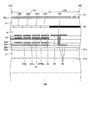
(第1の実施形態)
図1は、第1の実施形態に係るタッチ検出機能付き表示装置の一構成例を示すブロック図である。図1に示すように、タッチ検出機能付き表示装置1は、タッチ検出機能付き表示部10と、制御部11と、ゲートドライバ12と、ソースドライバ13と、駆動電極ドライバ14と、検出部40とを備えている。タッチ検出機能付き表示装置1は、タッチ検出機能付き表示部10がタッチ検出機能を内蔵した表示装置である。タッチ検出機能付き表示部10は、表示素子として液晶表示素子を用いている表示パネル20と、タッチ入力を検出する検出装置であるタッチパネル30とを一体化した装置である。なお、タッチ検出機能付き表示部10は、表示パネル20の上にタッチパネル30を装着した、いわゆるオンセルタイプの装置であってもよい。表示パネル20は、例えば、有機EL表示パネルであってもよい。
(First embodiment)
FIG. 1 is a block diagram illustrating a configuration example of a display device with a touch detection function according to the first embodiment. As shown in FIG. 1, the display device with a
表示パネル20は、後述するように、ゲートドライバ12から供給される走査信号Vscanに従って、1水平ラインずつ順次走査して表示を行う素子である。制御部11は、外部より供給された映像信号Vdispに基づいて、ゲートドライバ12、ソースドライバ13、駆動電極ドライバ14及び検出部40に対してそれぞれ制御信号を供給し、これらが互いに同期して動作するように制御する回路である。
As will be described later, the
ゲートドライバ12は、制御部11から供給される制御信号に基づいて、タッチ検出機能付き表示部10の表示駆動の対象となる1水平ラインを順次選択する機能を有している。
The
ソースドライバ13は、制御部11から供給される制御信号に基づいて、タッチ検出機能付き表示部10の、後述する各副画素SPixに画素信号Vpixを供給する回路である。
The
駆動電極ドライバ14は、制御部11から供給される制御信号に基づいて、タッチ検出機能付き表示部10の、後述する駆動電極COMLに第1駆動信号Vcomを供給する回路である。
The
タッチパネル30は、静電容量型タッチ検出の基本原理に基づいて動作し、相互静電容量方式によりタッチ検出動作を行い、表示領域に対する外部の導体の接触又は近接を検出する。タッチパネル30は、自己静電容量方式によりタッチ検出動作を行ってもよい。
The
検出部40は、制御部11から供給される制御信号と、タッチパネル30から供給される第1検出信号Vdet1に基づいて、タッチパネル30に対するタッチの有無を検出する回路である。また、検出部40は、タッチがある場合においてタッチ入力が行われた座標などを求める。この検出部40は、検出信号増幅部42と、A/D変換部43と、信号処理部44と、座標抽出部45とを備える。検出タイミング制御部46は、制御部11から供給される制御信号に基づいて、A/D変換部43と、信号処理部44と、座標抽出部45とが同期して動作するように制御する。
The
さらに、検出部40は、第2検出電極ドライバ48を含む。第2検出電極ドライバ48は、タッチ検出機能付き表示部10に加えられた圧力を検出する際に、後述する第2検出電極23に第2駆動信号Vdを供給する回路である。検出部40は、第2検出電極23から供給される第2検出信号Vdet2に基づいて、タッチ検出機能付き表示部10に加えられた圧力を検出する。
Further, the
上述のとおり、タッチパネル30は、静電容量型タッチ検出の基本原理に基づいて動作する。ここで、図2から図8を参照して、本実施形態のタッチ検出機能付き表示装置1の相互静電容量方式によるタッチ検出の基本原理について説明する。図2は、相互静電容量方式のタッチ検出の基本原理を説明するための、指が接触又は近接していない状態を表す説明図である。図3は、図2に示す指が接触又は近接していない状態のフリンジ電界の例を示す説明図である。図4は、図2に示す指が接触又は近接していない状態の等価回路の例を示す説明図である。図5は、相互静電容量方式のタッチ検出の基本原理を説明するための、指が接触又は近接した状態を表す説明図である。図6は、図5に示す指が接触又は近接した状態のフリンジ電界の例を示す説明図である。図7は、図5に示す指が接触又は近接した状態の等価回路の例を示す説明図である。図8は、駆動信号及び第1検出信号の波形の一例を表す図である。なお、以下の説明では、指が接触又は近接する場合を説明するが、指に限られず、例えばスタイラスペン等の導体を含む物体であってもよい。
As described above, the
例えば、図2に示すように、容量素子C1は、誘電体Dを挟んで互いに対向配置された一対の電極、駆動電極E1及び検出電極E2を備えている。容量素子C1は、駆動電極E1と検出電極E2との対向面同士の間に形成される電気力線(図示しない)に加え、図3に示すように、駆動電極E1の端部から検出電極E2の上面に向かって延びるフリンジ電界Efが生じる。図4に示すように、容量素子C1は、その一端が交流信号源(駆動信号源)Sに接続され、他端は電圧検出器DETに接続される。電圧検出器DETは、例えば図1に示す検出信号増幅部42に含まれる積分回路である。
For example, as shown in FIG. 2, the capacitive element C <b> 1 includes a pair of electrodes, a drive electrode E <b> 1, and a detection electrode E <b> 2 that are opposed to each other with the dielectric D interposed therebetween. In addition to the electric lines of force (not shown) formed between the opposing surfaces of the drive electrode E1 and the detection electrode E2, the capacitive element C1 has a detection electrode E2 from the end of the drive electrode E1, as shown in FIG. A fringe electric field Ef extending toward the upper surface of the substrate is generated. As shown in FIG. 4, the capacitive element C1 has one end connected to an AC signal source (drive signal source) S and the other end connected to a voltage detector DET. The voltage detector DET is, for example, an integration circuit included in the detection
交流信号源Sから駆動電極E1(容量素子C1の一端)に所定の周波数(例えば数kHz〜数百kHz程度)の交流矩形波Sgが印加されると、検出電極E2(容量素子C1の他端)側に接続された電圧検出器DETを介して、図8に示すような出力波形(第1検出信号Vdet1)が現れる。なお、この交流矩形波Sgは、駆動電極ドライバ14から入力される第1駆動信号Vcomに相当するものである。
When an AC rectangular wave Sg having a predetermined frequency (for example, about several kHz to several hundred kHz) is applied from the AC signal source S to the drive electrode E1 (one end of the capacitive element C1), the detection electrode E2 (the other end of the capacitive element C1) The output waveform (first detection signal Vdet1) as shown in FIG. 8 appears via the voltage detector DET connected to the) side. The AC rectangular wave Sg corresponds to the first drive signal Vcom input from the
指が接触又は近接していない状態(非接触状態)では、図4に示すように、容量素子C1に対する充放電に伴って、容量素子C1の容量値に応じた電流I0が流れる。図4に示す電圧検出器DETは、交流矩形波Sgに応じた電流I0の変動を電圧の変動(実線の波形V0(図8参照))に変換する。 In a state where the finger is not in contact with or in close proximity (non-contact state), as shown in FIG. 4, a current I 0 corresponding to the capacitance value of the capacitive element C1 flows along with charging / discharging of the capacitive element C1. The voltage detector DET shown in FIG. 4 converts the fluctuation of the current I 0 according to the AC rectangular wave Sg into a fluctuation of voltage (solid line waveform V 0 (see FIG. 8)).
一方、指が接触又は近接した状態(接触状態)では、図5に示すように、指によって形成される静電容量C2が、検出電極E2と接触している又は近傍にある。これにより、図6に示すように駆動電極E1と検出電極E2との間にあるフリンジ電界Efが導体E3(指)により遮られる。このため、容量素子C1は、図7に示すように、非接触状態での容量値よりも容量値の小さい容量素子C1’として作用する。そして、図7に示す等価回路でみると、容量素子C1’に電流I1が流れる。図8に示すように、電圧検出器DETは、交流矩形波Sgに応じた電流I1の変動を電圧の変動(点線の波形V1)に変換する。この場合、波形V1は、上述した波形V0と比べて振幅が小さくなる。これにより、波形V0と波形V1との電圧差分の絶対値|ΔV|は、指などの外部から接触又は近接する導体E3の影響に応じて変化することになる。なお、電圧検出器DETは、波形V0と波形V1との電圧差分の絶対値|ΔV|を精度よく検出するため、回路内のスイッチングにより、交流矩形波Sgの周波数に合わせて、コンデンサの充放電をリセットする期間Resetを設けた動作とすることがより好ましい。 On the other hand, when the finger is in contact or in proximity (contact state), as shown in FIG. 5, the capacitance C2 formed by the finger is in contact with or in the vicinity of the detection electrode E2. As a result, as shown in FIG. 6, the fringe electric field Ef between the drive electrode E1 and the detection electrode E2 is blocked by the conductor E3 (finger). Therefore, as shown in FIG. 7, the capacitive element C1 acts as a capacitive element C1 ′ having a smaller capacitance value than the capacitance value in the non-contact state. In the equivalent circuit shown in FIG. 7, the current I 1 flows through the capacitive element C1 ′. As shown in FIG. 8, the voltage detector DET converts the fluctuation of the current I 1 according to the AC rectangular wave Sg into the fluctuation of the voltage (dotted line waveform V 1 ). In this case, the waveform V 1 has a smaller amplitude than the waveform V 0 described above. As a result, the absolute value | ΔV | of the voltage difference between the waveform V 0 and the waveform V 1 changes according to the influence of the conductor E3 that is in contact with or close to the outside such as a finger. Note that the voltage detector DET accurately detects the absolute value | ΔV | of the voltage difference between the waveform V 0 and the waveform V 1 , so that the capacitance of the capacitor is adjusted according to the frequency of the AC rectangular wave Sg by switching in the circuit. More preferably, the operation is provided with a reset period during which the charge / discharge is reset.
図1に示すタッチパネル30は、駆動電極ドライバ14から供給される第1駆動信号Vcomに従って、1検出ブロックずつ順次走査して、相互静電容量方式によるタッチ検出を行う。
The
タッチパネル30は、後述する複数の第1検出電極TDLから、図4又は図7に示す電圧検出器DETを介して、検出ブロック毎に第1検出信号Vdet1を出力する。第1検出信号Vdet1は、検出部40の検出信号増幅部42に供給される。
The
検出信号増幅部42は、タッチパネル30から供給される第1検出信号Vdet1を増幅する。なお、検出信号増幅部42は、第1検出信号Vdet1に含まれる高い周波数成分(ノイズ成分)を除去して出力する低域通過アナログフィルタであるアナログLPF(Low Pass Filter)を備えていてもよい。
The
A/D変換部43は、第1駆動信号Vcomに同期したタイミングで、検出信号増幅部42から出力されるアナログ信号をそれぞれサンプリングしてデジタル信号に変換する。
The A /
信号処理部44は、A/D変換部43の出力信号に含まれる、第1駆動信号Vcomをサンプリングした周波数以外の周波数成分(ノイズ成分)を低減するデジタルフィルタを備えている。信号処理部44は、A/D変換部43の出力信号に基づいて、タッチパネル30に対するタッチの有無を検出する論理回路である。信号処理部44は、指による検出信号の差分のみ取り出す処理を行う。この指による差分の信号は、上述した波形V0と波形V1との差分の絶対値|ΔV|である。信号処理部44は、1検出ブロック当たりの絶対値|ΔV|を平均化する演算を行い、絶対値|ΔV|の平均値を求めてもよい。これにより、信号処理部44は、ノイズによる影響を低減できる。信号処理部44は、検出した指による差分の信号を所定のしきい値電圧と比較し、このしきい値電圧未満であれば、外部近接物体が非接触状態であると判断する。一方、信号処理部44は、検出した指による差分の信号を所定のしきい値電圧と比較し、しきい値電圧以上であれば、外部近接物体の接触状態と判断する。このようにして、検出部40はタッチ検出が可能となる。
The
座標抽出部45は、信号処理部44においてタッチが検出されたときに、そのタッチパネル座標を求める論理回路である。座標抽出部45は、タッチパネル座標を検出信号出力Voutとして出力する。以上のように、本実施形態のタッチ検出機能付き表示装置1は、相互静電容量方式によるタッチ検出の基本原理に基づいて、指などの導体が接触又は近接する位置のタッチパネル座標を検出することができる。
The coordinate
次に、図9及び図10を参照して、自己静電容量方式のタッチ検出の基本原理について説明する。図9は、自己静電容量方式のタッチ検出の等価回路の一例を示す説明図である。図10は、自己静電容量方式のタッチ検出の駆動信号及び第2検出信号の波形の一例を表す図である。 Next, the basic principle of the self-capacitance touch detection will be described with reference to FIGS. FIG. 9 is an explanatory diagram illustrating an example of an equivalent circuit for self-capacitance touch detection. FIG. 10 is a diagram illustrating an example of waveforms of the drive signal and the second detection signal for the self-capacitance type touch detection.
図9に示すように、検出電極E2に電圧検出器DETが接続されている。電圧検出器DETはイマジナリーショートされたオペアンプを含む検出回路である。非反転入力部(+)に所定の周波数(例えば数kHz〜数百kHz程度)の交流矩形波Sgが印加されると、検出電極E2に同電位の交流矩形波Sgが印加される。 As shown in FIG. 9, a voltage detector DET is connected to the detection electrode E2. The voltage detector DET is a detection circuit including an imaginary short-circuited operational amplifier. When an AC rectangular wave Sg having a predetermined frequency (for example, about several kHz to several hundred kHz) is applied to the non-inverting input unit (+), an AC rectangular wave Sg having the same potential is applied to the detection electrode E2.
指などの導体が接触又は近接していない状態(非接触状態)では、検出電極E2が有する容量Cx1に応じた電流が流れる。電圧検出器DETは、交流矩形波Sgに応じた電流の変動を電圧の変動(実線の波形V3(図10参照))に変換する。指などの導体が接触又は近接した状態(接触状態)では、検出電極E2が有する容量Cx1に、検出電極E2に近接している指により生じる容量Cx2が加えられ、非接触状態の容量よりも増加した容量(Cx1+Cx2)に応じた電流が流れる。電圧検出器DETは、交流矩形波Sgに応じた電流の変動を電圧の変動(点線の波形V2(図10参照))に変換する。この場合、波形V2は、上述した波形V3と比べて振幅が大きくなる。これにより、波形V2と波形V3との電圧差分の絶対値|ΔV|は、指などの外部から接触又は近接する導体の影響に応じて変化することになる。スイッチSWは、タッチ検出を行う際にオン(開)状態となり、タッチ検出を行わないときはオフ(閉)状態となり、電圧検出器DETのリセット動作を行う。 In a state where a conductor such as a finger is not in contact with or in close proximity (non-contact state), a current corresponding to the capacitance Cx1 of the detection electrode E2 flows. The voltage detector DET converts a current fluctuation according to the AC rectangular wave Sg into a voltage fluctuation (solid line waveform V 3 (see FIG. 10)). In a state in which a conductor such as a finger is in contact or in proximity (contact state), the capacitance Cx2 generated by the finger in proximity to the detection electrode E2 is added to the capacitance Cx1 of the detection electrode E2, which is larger than the capacitance in the non-contact state. A current corresponding to the capacity (Cx1 + Cx2) flows. The voltage detector DET converts a current fluctuation according to the AC rectangular wave Sg into a voltage fluctuation (dotted line waveform V 2 (see FIG. 10)). In this case, the waveform V 2 has a larger amplitude than the waveform V 3 described above. As a result, the absolute value | ΔV | of the voltage difference between the waveform V 2 and the waveform V 3 changes according to the influence of a conductor that is in contact with or close to the outside such as a finger. The switch SW is turned on (open) when touch detection is performed, and is turned off (closed) when touch detection is not performed, and performs a reset operation of the voltage detector DET.
検出信号増幅部42は、タッチパネル30から供給された第2検出信号Vdet2を増幅する。A/D変換部43は、検出信号増幅部42から出力されるアナログ信号をそれぞれサンプリングしてデジタル信号に変換する。信号処理部44は、A/D変換部43から供給される信号に基づいて、波形V2と波形V3との差分の絶対値|ΔV|を演算する。信号処理部44は、検出した指による差分の信号(絶対値|ΔV|)を所定のしきい値電圧と比較し、このしきい値電圧未満であれば、外部近接物体が非接触状態であると判断する。一方、信号処理部44は、検出した指による差分の信号(絶対値|ΔV|)を所定のしきい値電圧と比較し、しきい値電圧以上であれば、外部近接物体の接触状態と判断する。座標抽出部45は、タッチパネル座標を演算し、検出信号出力Voutとして出力する。このようにして、検出部40は自己静電容量方式のタッチ検出の基本原理に基づいてタッチ検出が可能となる。
The
電圧検出器DETは、相互静電容量方式のタッチ検出と、自己静電容量方式のタッチ検出とに兼用してもよい。この場合、相互静電容量方式のタッチ検出の際に、非反転入力部(+)に固定された電位を有する基準電圧が入力され、自己静電容量方式のタッチ検出の際に、非反転入力部(+)に交流矩形波Sg(第1駆動信号Vcom)が入力されるように切り替えられる。 The voltage detector DET may be used both for mutual capacitance type touch detection and for self-capacitance type touch detection. In this case, a reference voltage having a fixed potential is input to the non-inverting input unit (+) when the mutual capacitance type touch detection is performed, and a non-inverting input is performed when the self-capacitance type touch detection is performed. It is switched so that the AC rectangular wave Sg (first drive signal Vcom) is input to the part (+).
図9及び図10は、指が接触又は近接した場合の外部近接物体の検出について説明したが、検出電極E2と対向する導電体を設け、上述した自己静電容量方式の検出原理に基づいて、入力面に加えられた圧力を検出することができる。この場合、タッチ検出機能付き表示部10の入力面に加えられた圧力に応じて検出電極E2と導電体との間の距離が変化し、検出電極E2と導電体との間に形成される容量が変化する。タッチパネル30は、この容量変化に応じた第2検出信号Vdet2を検出信号増幅部42に出力する。検出信号増幅部42、A/D変換部43及び信号処理部44は、上述の信号処理を行い、波形V2と波形V3との差分の絶対値|ΔV|を演算する。絶対値|ΔV|の値に基づいて、検出電極E2と導電体との間の距離が求められる。これにより、入力面に加えられた圧力が算出される。座標抽出部45は、入力面に入力された圧力の分布と、タッチ検出により求められたタッチパネル座標から、入力位置における圧力を演算し、圧力の情報を出力する。
FIG. 9 and FIG. 10 describe detection of an external proximity object when a finger contacts or approaches, based on the above-described detection principle of the self-capacitance method by providing a conductor facing the detection electrode E2. The pressure applied to the input surface can be detected. In this case, the distance between the detection electrode E2 and the conductor changes according to the pressure applied to the input surface of the
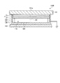
図11は、タッチ検出機能付き表示装置を含む電子機器の概略断面構造を表す断面図である。電子機器100は、カバー部材101と、タッチ検出機能付き表示装置1と、バックライト102と、筐体103とを含む。カバー部材101は、タッチ検出機能付き表示装置1を保護するための保護部材であり、例えば、透光性を有するガラス基板や、樹脂材料等を用いたフィルム状の基材であってもよい。カバー部材101の一方の面が、指等が接触又は近接して入力操作を行うための入力面101aとなっている。タッチ検出機能付き表示装置1は、後述する画素基板2と、対向基板3とを含む。画素基板2の上に対向基板3が設けられており、対向基板3は、カバー部材101の他方の面、すなわち入力面101aの反対側の面に配置される。
FIG. 11 is a cross-sectional view illustrating a schematic cross-sectional structure of an electronic device including a display device with a touch detection function. The
バックライト102は、タッチ検出機能付き表示装置1に対してカバー部材101の反対側に設けられる。バックライト102は、画素基板2の下面側に接着されていてもよく、画素基板2と所定の間隔を設けて配置されていてもよい。バックライト102は、例えばLED(Light Emitting Diode)等の光源を有しており、光源からの光を画素基板2に向けて射出する。バックライト102からの光は、画素基板2を通過して、その位置の液晶の状態により光が遮られて射出しない部分と射出する部分とが切り換えられることで、カバー部材101の入力面101aに画像が表示される。バックライト102は、公知の照明部を用いることができ、種々の構成が適用可能である。また、タッチ検出機能付き表示装置1の表示パネル20が反射型液晶表示装置である場合、バックライト102は設けなくてもよい。反射型液晶表示装置は、画素基板2に反射電極が設けられ、カバー部材101側から入射する光が反射電極によって反射されて、カバー部材101を通過して観察者の目に到達する。また、バックライト102に替えてフロントライトを設けてもよい。
The
筐体103は上部に開口を有する箱状の部材であり、筐体103の開口を覆うようにカバー部材101が設けられる。筐体103とカバー部材101とで形成される内部空間にタッチ検出機能付き表示装置1、バックライト102等が組み込まれる。図11に示すように、タッチ検出機能付き表示装置1及びバックライト102は、カバー部材101側に配置され、バックライト102と筐体103の底部との間に空隙110が設けられている。筐体103は金属などの導電性材料が用いられ、筐体103の底部が、タッチ検出機能付き表示装置1の第2検出電極23(図示しない)と対向する導電体104として機能する。また、筐体103は、グラウンドに電気的に接続されて接地される。このような構成により、タッチ検出機能付き表示装置1の第2検出電極23(図示しない)と導電体104との間に容量C3が形成される。
The
入力面101aに圧力が加えられると、画素基板2及び対向基板3は、カバー部材101とともに筐体103の底部側にわずかに撓むように変形する。タッチ検出機能付き表示装置1は、上述した自己静電容量方式の検出原理に基づいて容量C3の変化を検出することにより、カバー部材101、タッチ検出機能付き表示装置1及びバックライト102の撓み量が求められる。これにより、入力面101aに入力された圧力が得られる。
When pressure is applied to the
バックライト102と筐体103の底部との間の空隙110には、入力された圧力に応じて変形可能な、スポンジや弾性ゴム等の弾性体を設けてもよい。また、筐体103は金属などの導電性材料に限定されず、樹脂等の絶縁性材料を用いてもよい。この場合、筐体103の少なくとも底部に金属層を設けて導電体104としてもよい。
In the
図12は、第1変形例に係る電子機器の概略断面構造を表す断面図である。本変形例では、表示装置用筐体107が設けられている。表示装置用筐体107の開口を覆うようにカバー部材101が設けられ、表示装置用筐体107とカバー部材101との内部空間にタッチ検出機能付き表示装置1及びバックライト102が組み込まれる。タッチ検出機能付き表示装置1は、カバー部材101の入力面101aに対して反対側の面に設けられる。バックライト102は、表示装置用筐体107の底部に設けられる。タッチ検出機能付き表示装置1とバックライト102との間にスペーサ106が設けられており、タッチ検出機能付き表示装置1とバックライト102との間に空隙110が形成される。表示装置用筐体107が電子機器100Aの筐体103に固定されることで、表示装置用筐体107、カバー部材101、タッチ検出機能付き表示装置1及びバックライト102が一体となって電子機器100Aに組み込まれる。
FIG. 12 is a cross-sectional view illustrating a schematic cross-sectional structure of an electronic device according to a first modification. In this modification, a
本変形例において、表示装置用筐体107は金属などの導電性材料が用いられる。これにより、表示装置用筐体107の底部が導電体104として機能する。また、表示装置用筐体107は、グラウンドに電気的に接続されて接地される。このような構成により、導電体104とタッチ検出機能付き表示装置1の第2検出電極23(図示しない)との間に容量C4が形成される。タッチ検出機能付き表示装置1は、上述した自己静電容量方式の検出原理に基づいて容量C4の変化を検出することにより、入力面101aに入力される圧力を検出することができる。
In this modification, the
本変形例では、表示装置用筐体107が金属などの導電性材料であり、底部が導電体104として機能するが、これに限定されない。表示装置用筐体107に樹脂材料等の絶縁材料を用い、表示装置用筐体107の少なくとも底部に金属層を設けて導電体104としてもよい。また、バックライト102の下面(表示装置用筐体107の底部と対向する面)に金属層を設けてもよい。表示装置用筐体107は電子機器100Aの筐体103の上に固定されているが、固定構造は特に限定されず、例えば、カバー部材101が筐体103に固定されていてもよい。
In this modification, the
図13は、第2変形例に係る電子機器の概略断面構造を表す断面図である。本変形例の電子機器100Bにおいて、表示装置用筐体107とカバー部材101との内部空間にタッチ検出機能付き表示装置1及びバックライト102が組み込まれる。タッチ検出機能付き表示装置1は、カバー部材101の入力面101aに対し反対側の面に設けられる。バックライト102は、タッチ検出機能付き表示装置1のカバー部材101と反対側の面に設けられている。バックライト102と表示装置用筐体107との間にスペーサ106が設けられており、バックライト102と表示装置用筐体107との間に空隙110が形成される。
FIG. 13 is a cross-sectional view illustrating a schematic cross-sectional structure of an electronic device according to a second modification. In the
本変形例においても、表示装置用筐体107の底部が導電体104として機能し、導電体104とタッチ検出機能付き表示装置1の検出電極(図示しない)との間に容量C5が形成される。タッチ検出機能付き表示装置1は、上述した自己静電容量方式の検出原理に基づいて容量C5の変化を検出することにより、入力面101aに入力される圧力を検出することができる。
Also in this modification, the bottom of the display device casing 107 functions as the
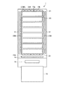
次に、タッチ検出機能付き表示装置1の構成例を詳細に説明する。図14は、第1の実施形態に係るタッチ検出機能付き表示装置の概略断面構造を表す断面図である。図15は、タッチ検出機能付き表示装置の第1基板を模式的に示す平面図である。図16は、タッチ検出機能付き表示装置の第2基板を模式的に示す平面図である。
Next, a configuration example of the
図14に示すように、タッチ検出機能付き表示部10は、画素基板2と、この画素基板2の表面に垂直な方向に対向して配置された対向基板3と、画素基板2と対向基板3との間に挿設された表示機能層としての液晶層6とを備える。
As shown in FIG. 14, the
画素基板2は、回路基板としての第1基板21と、画素電極22と、第2検出電極23と、駆動電極COMLと、絶縁層24と、を含む。第1基板21には、スイッチング素子であるTFT(Thin Film Transistor)が画素電極22に対応して配置される。画素電極22は、第1基板21の上方に設けられ、平面視でマトリックス状に複数配設される。第2検出電極23は、圧力を検出するための検出電極である。駆動電極COMLは、第1基板21と画素電極22との間に複数設けられる。絶縁層24は、画素電極22と駆動電極COMLとを絶縁する。第1基板21の下側には、接着層66Bを介して偏光板65Bが設けられていてもよい。
The
第1基板21には、表示制御用IC19が設けられている。表示制御用IC19は、第1基板21にCOG(Chip On Glass)実装されたチップであり、上述した制御部11を内蔵したものである。また、第1基板21の端部にフレキシブル基板72が接続されている。表示制御用IC19は、外部のホストIC(図示しない)から供給された映像信号Vdisp(図1参照)に基づいて、後述する走査信号線GCL及び画素信号線SGL等に制御信号を出力する。
The
対向基板3は、第2基板31と、第2基板31の一方の面に形成されたカラーフィルタ32とを含む。第2基板31の他方の面には、タッチパネル30の検出電極である第1検出電極TDLが設けられている。第1検出電極TDLの上には保護層39が設けられている。さらに、第1検出電極TDLの上方には、接着層66Aを介して偏光板65Aが設けられている。また、第2基板31にはフレキシブル基板71が接続されている。フレキシブル基板71は後述する額縁配線37を介して第1検出電極TDLと接続される。なお、カラーフィルタ32は第1基板21上に配置されてもよい。また、第1基板21と第2基板31は、例えば、ガラス基板である。
The
第1基板21と第2基板31とは、スペーサ61を介して所定の間隔を設けて対向して配置される。第1基板21と第2基板31との間の空間に液晶層6が設けられる。液晶層6は、電界の状態に応じてそこを通過する光を変調するものであり、例えば、FFS(フリンジフィールドスイッチング)を含むIPS(インプレーンスイッチング)等の横電界モードの液晶が用いられる。なお、図14に示す液晶層6と画素基板2との間、及び液晶層6と対向基板3との間には、それぞれ配向膜が配設されてもよい。
The
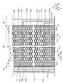
図15に示すように、タッチ検出機能付き表示装置1は、画像を表示させるための表示領域10aと、表示領域10aの外側の額縁領域10bとを有する。表示領域10aは、対向する2つの長辺と短辺とを有する矩形状である。額縁領域10bは、表示領域10aの4辺を囲む枠状となっている。本発明に関わる表示領域10aは、画像が表示される領域であって、例えば、液晶層6や白色OLED層により画像表示を行う場合には、カラーフィルタ32上の透過領域であり、反射型表示装置の場合は入射光が反射する反射領域であり、また、例えば、有色OLEDにより画像表示を行う場合には、発色可能な発光素子が配置された領域を指す。
As shown in FIG. 15, the display device with a
複数の駆動電極COMLは、第1基板21の表示領域10aに設けられている。駆動電極COMLは、表示領域10aの長辺に沿った方向に延在しており、表示領域10aの短辺に沿った方向に、複数配列されている。駆動電極COMLは、例えば、ITO(Indium Tin Oxide)等の透光性を有する導電性材料が用いられる。
The plurality of drive electrodes COML are provided in the
第2検出電極23は、表示領域10aの長辺及び短辺に沿った方向に複数配列されている。表示領域10aの長辺に沿った方向に配列された第2検出電極23を第2検出電極23Aとし、表示領域10aの短辺に沿った方向に配列された第2検出電極23を第2検出電極23Bとして表す。第2検出電極23Aと第2検出電極23Bとは、表示領域10aの周囲を囲んで配置されている。また、第2検出電極23Aと第2検出電極23Bとは、表示領域10aの少なくとも2辺を囲んでいればよい。第2検出電極23A及び第2検出電極23Bはそれぞれ矩形状を有している。第2検出電極23Aは、1本の駆動電極COMLに沿って複数配列されており、駆動電極COMLの延在方向における長さよりも第2検出電極23Aの長辺の長さが短い。
A plurality of
第1基板21の額縁領域10bの短辺側に、駆動電極ドライバ14及び表示制御用IC19が配置され、額縁領域10bの長辺側にゲートドライバ12が配置されている。また、額縁領域10bの短辺側に、フレキシブル基板72が接続されている。駆動電極ドライバ14及びフレキシブル基板72は、駆動電極COMLの延在方向の端部の近傍に配置されている。このため、駆動電極COMLから引き出される配線の長さを短くして、額縁領域10bの面積を小さくすることが可能である。
The
図16に示すように、第2基板31の表示領域10aに、第1検出電極TDLが設けられている。第1検出電極TDLは、表示領域10aの短辺に沿った方向に延在し、表示領域10aの長辺に沿った方向に複数配列される。第1検出電極TDLは、それぞれ複数の金属配線33a、33bを有している。複数の金属配線33a、33bは、複数の屈曲部を有してジグザグ線又は波線に形成されており、表示領域10aの短辺に沿った方向に延在する。金属配線33aと金属配線33bとが表示領域10aの長辺に沿った方向に交互に配列される。本実施形態では、金属配線33aの屈曲部と金属配線33bの屈曲部とが互いに接続されて、第1検出電極TDLがメッシュ状の金属配線として構成される。金属配線33a及び金属配線33bは、図16の点線Aに示す箇所に設けられたスリットSLにより分離される。スリットSLで分離された金属配線33a及び金属配線33bが、それぞれ1つの第1検出電極TDLとして機能する。
As shown in FIG. 16, the first detection electrode TDL is provided in the
本実施形態では、額縁領域10bの短辺に、第1検出電極TDLと離隔して導電層35が設けられている。導電層35は、複数の金属配線33a、33bを有しておりメッシュ状となっている。導電層35は、図15に示す第2検出電極23Bと重畳する位置に設けられている。このため、第2検出電極23Bに供給される第2駆動信号Vdと同期した同一の波形のガード信号Vsglが導電層35に供給されることで、第2検出電極23Bに発生する寄生容量を低減することができる。また、第1検出電極TDLの端部は、第2検出電極23Aに重畳して設けられているため、第2検出電極23Aにもガード信号Vsglが供給されることで第2検出電極23Aに発生する寄生容量を低減することができる。
In the present embodiment, the
金属配線33a、33bは、アルミニウム(Al)、銅(Cu)、銀(Ag)、モリブデン(Mo)又はこれらの合金の少なくとも1つの金属材料で形成される。また、金属配線33a、33bは、これらの金属材料を1以上用いて、複数積層した積層体としてもよい。アルミニウム(Al)、銅(Cu)、銀(Ag)又はこれらの合金の少なくとも1つの金属材料は、透光性電極の材料としてITO等の透光性導電酸化物よりも低抵抗である。アルミニウム(Al)、銅(Cu)、銀(Ag)又はこれらの合金の少なくとも1つの金属材料は、ITO等の透光性導電酸化物に比較して遮光性があるため、透過率が低下する可能性又は第1検出電極TDLのパターンが視認されてしまう可能性がある。本実施形態において、1つの第1検出電極TDLが、複数の幅細の金属配線33a、33bを有しており、金属配線33a、33bが、線幅よりも大きい間隔を設けてメッシュ状に配置されることで、低抵抗化と、不可視化とを実現することができる。その結果、第1検出電極TDLが低抵抗化し、タッチ検出機能付き表示装置1は、薄型化、大画面化又は高精細化することができる。
The
金属配線33a、33bの幅は、2μm以上かつ10μm以下の範囲にあることが好ましい。金属配線33a、33bの幅が10μm以下であると、表示領域10aのうちブラックマトリックス又は走査信号線GCL及び画素信号線SGLで光の透過を抑制されない領域である開口部を覆う面積が小さくなり、開口率を損なう可能性が低くなるからである。また、金属配線33a、33bの幅が2μm以上であると、形状が安定し、断線する可能性が低くなるからである。反射率を抑えるために、金属配線33a、33bの最表面に黒色化処理を行うことも好ましい。
The width of the
図16に示すように、第2基板31の額縁領域10bに、第1検出電極TDLから引き出された額縁配線37が複数設けられている。第2基板31の額縁領域10bの短辺側にフレキシブル基板71が接続されている。額縁配線37は、額縁領域10bの長辺に沿って延在して、フレキシブル基板71と接続される。フレキシブル基板71には、タッチ検出用IC18が搭載されている。タッチ検出用IC18は、図1に示す検出部40が実装されており、第1検出電極TDLから出力される第1検出信号Vdet1が、額縁配線37及びフレキシブル基板71を介してタッチ検出用IC18に供給される。
As shown in FIG. 16, in the
本実施形態では、検出部40はフレキシブル基板71に実装されたタッチドライバICであるが、検出部40の一部の機能は、他のMPUの機能として設けられてもよい。具体的には、タッチドライバICの機能として設けられ得るA/D変換、ノイズ除去等の各種機能のうち一部の機能(例えば、ノイズ除去等)は、タッチドライバICと別個に設けられたMPU(Micro−processing unit)等の回路で実施されてもよい。
In the present embodiment, the
フレキシブル基板71はコネクタ部72aを介してフレキシブル基板72と接続される。これにより、タッチ検出用IC18に実装された第2検出電極ドライバ48(図1参照)から第2検出電極23に、第2駆動信号Vdが供給されるようになっている。また、第2検出電極23から出力される第2検出信号Vdet2がタッチ検出用IC18に供給される。
The
次に表示パネル20の表示動作について説明する。図17は、第1の実施形態に係るタッチ検出機能付き表示部の画素配列を表す回路図である。第1基板21(図14参照)には、図17に示す各副画素SPixの薄膜トランジスタ素子(以下、TFT素子)Tr、各画素電極22に画素信号Vpixを供給する画素信号線SGL、各TFT素子Trを駆動する駆動信号を供給する走査信号線GCL等の配線が形成されている。画素信号線SGL及び走査信号線GCLは、第1基板21の表面と平行な平面に延在する。
Next, the display operation of the
図17に示す表示パネル20は、マトリクス状に配列された複数の副画素SPixを有している。副画素SPixは、それぞれTFT素子Tr及び液晶素子LCを備えている。TFT素子Trは、薄膜トランジスタにより構成されるものであり、この例では、nチャネルのMOS(Metal Oxide Semiconductor)型のTFTで構成されている。TFT素子Trのソースは画素信号線SGLに接続され、ゲートは走査信号線GCLに接続され、ドレインは液晶素子LCの一端に接続されている。液晶素子LCは、一端がTFT素子Trのドレインに接続され、他端が駆動電極COMLに接続されている。
The
副画素SPixは、走査信号線GCLにより、表示パネル20の同じ行に属する他の副画素SPixと互いに接続されている。走査信号線GCLは、ゲートドライバ12(図1参照)と接続され、ゲートドライバ12より走査信号Vscanが供給される。また、副画素SPixは、画素信号線SGLにより、表示パネル20の同じ列に属する他の副画素SPixと互いに接続されている。画素信号線SGLは、ソースドライバ13(図1参照)と接続され、ソースドライバ13より画素信号Vpixが供給される。さらに、副画素SPixは、駆動電極COMLにより、同じ列に属する他の副画素SPixと互いに接続されている。駆動電極COMLは、駆動電極ドライバ14(図1参照)と接続され、駆動電極ドライバ14より第1駆動信号Vcomが供給される。つまり、この例では、同じ一列に属する複数の副画素SPixが一本の駆動電極COMLを共有するようになっている。本実施形態の駆動電極COMLの延びる方向は、画素信号線SGLの延びる方向と平行である。
The subpixel SPix is connected to another subpixel SPix belonging to the same row of the
図1に示すゲートドライバ12は、走査信号線GCLを順次走査するように駆動する。ゲートドライバ12は、走査信号線GCLを介して、走査信号Vscan(図1参照)を副画素SPixのTFT素子Trのゲートに印加することにより、副画素SPixのうちの1行(1水平ライン)を表示駆動の対象として順次選択する。また、ソースドライバ13は、選択された1水平ラインを構成する副画素SPixに、画素信号線SGLを介して画素信号Vpixを供給する。そして、これらの副画素SPixでは、供給される画素信号Vpixに応じて1水平ラインずつ表示が行われるようになっている。この表示動作を行う際、駆動電極ドライバ14は、駆動電極COMLに対して第1駆動信号Vcomを印加する。画素電極22は、表示動作の第1駆動信号Vcomにより共通電位が供給される。
The
図14に示すカラーフィルタ32は、例えば赤(R)、緑(G)、青(B)の3色に着色されたカラーフィルタの色領域が周期的に配列されていてもよい。上述した図17に示す各副画素SPixに、R、G、Bの3色の色領域32R、32G、32Bが1組として対応付けられ、3色の色領域32R、32G、32Bに対応する副画素SPixを1組として画素Pixが構成される。図14に示すように、カラーフィルタ32は、第1基板21と垂直な方向において、液晶層6と対向する。なお、カラーフィルタ32は、異なる色に着色されていれば、他の色の組み合わせであってもよい。また、カラーフィルタ32は、3色の組み合わせに限定されず、4色以上の組み合わせであってもよい。
In the
図17に示すように、本実施形態では、駆動電極COMLが画素信号線SGLの延在方向と平行な方向に延在し、走査信号線GCLの延在方向と交差する方向に延びている。このため、駆動電極COMLからの配線を額縁領域10bの短辺側(フレキシブル基板72側)に引き出すことが可能である(図15参照)。したがって、駆動電極COMLを画素信号線SGLと直交する方向に設けた場合と比較して、額縁領域10bの長辺側に駆動電極ドライバ14を設ける必要がなく、額縁領域10bの幅を小さくすることができる。なお、駆動電極COMLはこれに限定されず、例えば走査信号線GCLと平行な方向に延びていてもよい。
As shown in FIG. 17, in the present embodiment, the drive electrode COML extends in a direction parallel to the extending direction of the pixel signal line SGL and extends in a direction intersecting with the extending direction of the scanning signal line GCL. Therefore, the wiring from the drive electrode COML can be drawn out to the short side (the
図14及び図15に示す駆動電極COMLは、表示パネル20の複数の画素電極22に共通の電位を与える共通電極として機能するとともに、タッチパネル30の相互静電容量方式によるタッチ検出を行う際の駆動電極としても機能する。また、駆動電極COMLは、タッチパネル30の自己静電容量方式によるタッチ検出を行う際の検出電極として機能してもよい。図18は、第1の実施形態に係るタッチ検出機能付き表示部の駆動電極及び第1検出電極の一構成例を表す斜視図である。タッチパネル30は、画素基板2に設けられた駆動電極COMLと、対向基板3に設けられた第1検出電極TDLにより構成されている。
The drive electrode COML shown in FIGS. 14 and 15 functions as a common electrode that applies a common potential to the plurality of
駆動電極COMLは、図18の左右方向に延在する複数のストライプ状の電極パターンを含む。第1検出電極TDLは、駆動電極COMLの電極パターンの延在方向と交差する方向に延びる複数の電極パターンを含む。そして、第1検出電極TDLは、第1基板21(図14参照)の表面に対する垂直な方向において、駆動電極COMLと対向している。第1検出電極TDLの各電極パターンは、検出部40の検出信号増幅部42の入力にそれぞれ接続される(図1参照)。駆動電極COMLの各電極パターンと第1検出電極TDLの各電極パターンとの交差部分に、それぞれ静電容量が形成される。
The drive electrode COML includes a plurality of striped electrode patterns extending in the left-right direction in FIG. The first detection electrode TDL includes a plurality of electrode patterns extending in a direction intersecting with the extending direction of the electrode pattern of the drive electrode COML. The first detection electrode TDL faces the drive electrode COML in a direction perpendicular to the surface of the first substrate 21 (see FIG. 14). Each electrode pattern of the first detection electrode TDL is connected to an input of the detection
第1検出電極TDL及び駆動電極COML(駆動電極ブロック)は、ストライプ状に複数に分割される形状に限られない。例えば、第1検出電極TDL及び駆動電極COMLは、櫛歯形状等であってもよい。あるいは第1検出電極TDL及び駆動電極COMLは、複数に分割されていればよく、駆動電極COMLを分割するスリットの形状は直線であっても、曲線であってもよい。 The first detection electrode TDL and the drive electrode COML (drive electrode block) are not limited to a shape divided into a plurality of stripes. For example, the first detection electrode TDL and the drive electrode COML may have a comb shape. Or the 1st detection electrode TDL and the drive electrode COML should just be divided | segmented into plurality, and the shape of the slit which divides | segments the drive electrode COML may be a straight line, or may be a curve.
この構成により、タッチパネル30では、相互静電容量方式のタッチ検出動作を行う際、駆動電極ドライバ14が駆動電極ブロックとして時分割的に順次走査するように駆動することにより、駆動電極COMLの1検出ブロックがスキャン方向Dsに沿って順次選択される。そして、第1検出電極TDLから第1検出信号Vdet1が出力されることにより、1検出ブロックのタッチ検出が行われるようになっている。つまり、駆動電極ブロックは、上述した相互静電容量方式のタッチ検出の基本原理における駆動電極E1に対応し、第1検出電極TDLは、検出電極E2に対応するものであり、タッチパネル30はこの基本原理に従ってタッチ入力を検出するようになっている。図18に示すように、タッチパネル30において、互いに交差した第1検出電極TDL及び駆動電極COMLは、静電容量式タッチセンサをマトリックス状に構成している。よって、タッチパネル30のタッチ検出面全体に亘って走査することにより、外部からの導体の接触又は近接が生じた位置の検出が可能となっている。
With this configuration, in the
図19は、第1の実施形態に係るタッチ検出機能付き表示装置の圧力検出を説明するための説明図である。上述したように、第1基板21と離隔して、第2検出電極23と対向する導電体104(筐体103、表示装置用筐体107等)が設けられており、第2検出電極23と導電体104との間に容量C6が形成される。カバー部材101(図11−図13参照)の入力面101aに圧力が加えられると、その圧力に応じてカバー部材101が導電体104側にわずかに撓むように変形する。そして、カバー部材101とともにタッチ検出機能付き表示装置1の第1基板21が撓むことで、第2検出電極23と導電体104との間隔が小さくなり、容量C6が増加する。
FIG. 19 is an explanatory diagram for explaining pressure detection of the display device with a touch detection function according to the first embodiment. As described above, the conductor 104 (the
上述した自己静電容量方式の検出原理に基づいて、第2検出電極23から第2検出信号Vdet2が出力される。つまり、第2検出電極23は、自己静電容量方式の検出原理における検出電極E2に対応する。第2検出電極23のそれぞれから出力された第2検出信号Vdet2に基づいて、入力面101aに加えられた圧力の大きさを検出することができる。第2検出電極23は、入力面101a側に物体が接触した際の圧力の強さ又は圧力の一次元座標を検出することができる。また、第2検出電極23A、23Bは、それぞれ個別電極として複数配列されているので、第2検出電極23A、23Bにより、入力面101aに加えられた圧力の分布を検出することもできる。本実施形態では、第1検出電極TDLに加えて第2検出電極23が設けられているので、外部の導体の接触又は近接が生じた位置を検出するとともに、検出された位置に加えられた圧力の大きさを検出することが可能となっている。タッチ検出機能付き表示装置1は、これらの検出結果を組み合わせてさまざまなアプリケーションへ反映させることができる。
Based on the detection principle of the self-capacitance method described above, the second detection signal Vdet2 is output from the
次に、第2検出電極23の構成について詳細に説明する。図20は、第1の実施形態に係る駆動電極及び第2検出電極を拡大して示す模式平面図である。図21は、図20のXXI−XXXI’線で切断したときの断面図である。図20に示すように、第2検出電極23Aは、額縁領域10bに設けられ、表示領域10aの長辺に沿って複数配列されている。第2検出電極23Bは、額縁領域10bに設けられ、表示領域10aの短辺に沿って複数配列されている。第2検出電極23A及び第2検出電極23Bは、それぞれコンタクトホールH1を介して接続配線38と接続される。第2検出電極23A及び第2検出電極23Bの形状や数は、あくまで一例であり、種々変更することができる。第2検出電極23Bは、駆動電極COMLと対応して配置されているが、これに限定されず、駆動電極COMLの数よりも多く設けてもよいし、少なくしてもよい。本明細書において「額縁領域10b」とは、第1基板21の外周よりも内側で、かつ、表示領域10aよりも外側の領域を示す。
Next, the configuration of the
駆動電極ドライバ14は、駆動電極走査部14aと、第1駆動信号生成部14bとを含む。第1駆動信号生成部14bは、第1駆動信号Vcomを生成して駆動電極走査部14aに供給する。上述した相互静電容量方式のタッチ検出を行う際に、駆動電極走査部14aは、駆動電極COMLの1検出ブロックを順次選択するように走査し、選択された1検出ブロックの駆動電極COMLに第1駆動信号Vcomを供給する。
The
駆動電極走査部14aは、接続配線38を介して、第2検出電極23A及び第2検出電極23Bと接続されており、第2検出電極23A及び第2検出電極23Bを順次、又は同時に選択する。第2検出電極ドライバ48(図1参照)に含まれる第2駆動信号生成部48aは、第2駆動信号Vdを生成して、駆動電極走査部14aに供給する。第2駆動信号生成部48aは、タッチ検出用IC18(図16参照)に実装されていてもよい。圧力検出を行う際に、駆動電極走査部14aは、検出対象となる第2検出電極23A及び第2検出電極23Bを選択して、選択された第2検出電極23A及び第2検出電極23Bに第2駆動信号Vdを供給する。それぞれの第2検出電極23A及び第2検出電極23Bから、導電体104との間の容量変化に応じた出力信号が検出部40に出力される。駆動電極走査部14aは、駆動電極COML、第2検出電極23A及び第2検出電極23Bに接続されているが、駆動電極COMLを走査する走査部と、第2検出電極23A及び第2検出電極23Bを走査する走査部とを別に設けてもよい。
The drive
本実施形態において、第2検出電極23A及び第2検出電極23Bが表示領域10aの周囲に複数設けられており、それぞれの第2検出電極23A及び第2検出電極23Bで圧力が検出されるため、精度よく圧力を検出することができる。例えば、駆動電極COMLを用いて圧力を検出する場合、駆動電極COMLの延在方向において圧力の情報の分解能がないため、駆動電極COMLの延在方向の圧力分布を検出することが困難な場合がある。本実施形態では、第2検出電極23Aは、表示領域10aの少なくとも1辺に沿って設けられ、駆動電極COMLの延在方向に沿って複数配列されているので、駆動電極COMLの延在方向に沿った方向の圧力分布を精度よく検出することができる。
In the present embodiment, a plurality of
すなわち、表示領域10aの周囲に沿って複数設けられた第2検出電極23A及び第2検出電極23Bと、駆動電極COMLとにより、異なる方向の圧力の座標を検出することが可能であり、これらの結果により加えられた圧力の二次元座標を算出することも可能である。この縦、横の圧力センサ(第2検出電極23A及び第2検出電極23B)を使って複数の点の圧力を算出することができる。さらに静電容量式のタッチパネル30で検出された指の座標、指の数等の情報を使うことで圧力センサ情報を補完することも容易である。額縁領域10bの圧力センサは左右、上下にセンサを配置し、左右の圧力センサ(第2検出電極23A)の圧力値と指の座標を比較することで指が押している場所の圧力値を算出できる。面内に圧力値の出力にバラツキがある場合は、あらかじめ補正テーブルを作成しておき、これと比較することで容易にバラツキを補正できる。
That is, it is possible to detect the coordinate of pressure in different directions by the plurality of
第2検出電極23A及び第2検出電極23Bは、表示領域10aの少なくとも2辺に沿って設けられていればよく、表示領域10a内にマトリクス状に電極を複数配置した場合に比べ、検出電極の数を少なくすることができる。したがって、タッチ検出用IC18や第2検出電極ドライバ48の構成を簡素化することができる。また、複数箇所で入力操作が行われた場合であっても、駆動電極COMLと第1検出電極TDLとで入力位置が検出されるので、入力位置の情報と圧力の情報から、各入力位置での圧力を算出することが可能である。
The
なお、本実施形態では、第2検出電極23A及び第2検出電極23Bは、額縁領域10bに設けられているが、これに限定されない。第2検出電極23A及び第2検出電極23Bは、表示領域10aに設けられていてもよく、表示領域10aと額縁領域10bとに跨って設けられていてもよい。
In the present embodiment, the
図21に示すように、第1基板21は第1面21aと、第1面21aの反対側の第2面21bとを有し、第1面21a側に絶縁層58a、絶縁層58bを介して走査信号線GCLが設けられている。接続配線38は、走査信号線GCLと同層に絶縁層58bの上に設けられている。接続配線38及び走査信号線GCLの上に絶縁層58cが設けられ、絶縁層58cの上に画素信号線SGLが設けられている。画素信号線SGLの上に平坦化層58dが設けられ、平坦化層58dの上に駆動電極COMLが設けられている。駆動電極COMLの上に複数の導電性配線51が設けられている。駆動電極COML及び導電性配線51の上に絶縁層24が設けられ、絶縁層24の上に画素電極22及び第2検出電極23が設けられる。第1基板21の第2面21b側には、第1基板21と離隔して導電体104が配置される。
As shown in FIG. 21, the
導電性配線51は、駆動電極COMLと接して、画素信号線SGLと重畳する位置に設けられている。導電性配線51は、第1検出電極TDLの金属配線33a、33bと同じ金属材料が用いられる。導電性配線51は、アルミニウム(Al)、銅(Cu)、銀(Ag)、モリブデン(Mo)又はこれらの合金の少なくとも1つの金属材料で形成される。導電性配線51を設けることにより、駆動電極COMLのみの場合に比べ、みかけ上の駆動電極COMLの抵抗値(駆動電極COMLと導電性配線51との合計の抵抗値)が低減される。
The
本実施形態では、第2検出電極23は、画素電極22と同層に設けられ、駆動電極COMLよりも第2基板31側の層に配置される。この場合、第2検出電極23は駆動電極COMLと重畳しない位置に設けられることが好ましい。これにより、第2検出電極23と導電体104との間の容量変化を精度よく検出することができる。また、第2検出電極23は、画素電極22と同じ材料を用いることができ、例えば、ITO等の透光性導電材料を用いることができる。
In the present embodiment, the
図21に示すように、第2基板31の表示領域10aには、カラーフィルタ32の各色領域32R、32G、32Bが設けられ、額縁領域10bには遮光層36が設けられている。第2基板31の上面に設けられた第1検出電極TDLは、第2検出電極23と重畳する位置まで延びて設けられていることが好ましい。こうすれば、圧力検出の際に、第2駆動信号Vdと同期した同一の波形を有するガード信号Vsglを第1検出電極TDLに供給することで、第1検出電極TDLがガード電極として機能し、第2検出電極23の寄生容量を低減できる。これにより、第2検出電極23に供給される第2駆動信号Vdを応答性の良い波形で駆動することができるので、検出感度の低下を抑制することができる。また、寄生容量のバラツキが小さくなるので、第2検出信号Vdet2の誤差を抑制して検出精度の低下を抑制できる。ガード信号Vsglは、第2駆動信号生成部48aから供給してもよいし、別の電源を用意して供給してもよい。
As shown in FIG. 21, the
次に、本実施形態のタッチ検出機能付き表示装置1の駆動方法について説明する。図22は、第1の実施形態に係るタッチ検出機能付き表示装置の一動作例を示すタイミング波形図である。
Next, a driving method of the display device with a
タッチ検出機能付き表示装置1の動作方法の一例として、タッチ検出機能付き表示装置1は、タッチ検出動作(タッチ検出期間)、圧力検出動作(圧力検出期間)及び表示動作(表示動作期間)を時分割に行う。タッチ検出動作、圧力検出動作及び表示動作はどのように分けて行ってもよいが、以下、表示パネル20の1フレーム期間(1F)、すなわち、1画面分の映像情報が表示されるのに要する時間の中において、タッチ検出動作、圧力検出動作及び表示動作をそれぞれ複数回に分割して行う方法について説明する。
As an example of an operation method of the
図22に示すように、制御信号(TS−VD)がオン(高レベル)になると1フレーム期間(1F)が開始される。制御信号(TS−HD)は、1フレーム期間(1F)にオン(高レベル)とオフ(低レベル)とが繰り返され、制御信号(TS−HD)がオンの期間内にタッチ検出動作又は圧力検出動作が実行され、オフの期間内に表示動作が実行される。制御信号(TS−VD)及び制御信号(TS−HD)は、制御部11(図1参照)のクロック生成部のクロック信号に基づいて出力される。1フレーム期間(1F)は、複数の表示動作期間Pdx(x=1、2、…n)と、タッチ検出動作を行う複数のタッチ検出期間Ptx(x=1、2、…m)と、圧力検出動作を行う複数の圧力検出期間Pf1、Pf2、Pf3とからなっている。これらの各期間は、時間軸上において、圧力検出期間Pf1、表示動作期間Pd1、タッチ検出期間Pt1、表示動作期間Pd2、タッチ検出期間Pt2、表示動作期間Pd3、…のように交互に配置されている。 As shown in FIG. 22, when the control signal (TS-VD) is turned on (high level), one frame period (1F) is started. The control signal (TS-HD) is repeatedly turned on (high level) and off (low level) in one frame period (1F), and the touch detection operation or pressure is within the period in which the control signal (TS-HD) is on. The detection operation is performed, and the display operation is performed within the off period. The control signal (TS-VD) and the control signal (TS-HD) are output based on the clock signal of the clock generation unit of the control unit 11 (see FIG. 1). One frame period (1F) includes a plurality of display operation periods Pd x (x = 1, 2,... N) and a plurality of touch detection periods Pt x (x = 1, 2,... M) for performing a touch detection operation. , And a plurality of pressure detection periods Pf 1 , Pf 2 , and Pf 3 for performing the pressure detection operation. Each of these periods includes a pressure detection period Pf 1 , a display operation period Pd 1 , a touch detection period Pt 1 , a display operation period Pd 2 , a touch detection period Pt 2 , a display operation period Pd 3 ,. Are alternately arranged.
制御部11は、ゲートドライバ12とソースドライバ13とを介して、各表示動作期間Pdxに選択される複数行の画素Pix(図17参照)に画素信号Vpixを供給する。図22は、RGBの3色を選択する選択信号(SELR/G/B)及び色毎の映像信号(SIGn)を示している。選択信号(SELR/G/B)に従って、対応する各副画素SPixが選択され、色毎の映像信号(SIGn)が選択された副画素SPixに供給されることにより、画像の表示動作が実行される。それぞれの表示動作期間Pdxで、1画面分の映像信号Vdispをn分割した画像が表示され、表示動作期間Pd1、Pd2、…Pdnで1画面分の映像情報が表示される。駆動電極COMLは表示パネル20の共通電極を兼用するので、駆動電極ドライバ14は、表示動作期間Pdxにおいて、選択される駆動電極COMLに対して表示駆動用の共通電位である第1駆動信号Vcomを供給する。
The
タッチ検出期間Ptx(x=1、2、…m)において、制御部11は、駆動電極ドライバ14に制御信号を出力する。駆動電極ドライバ14は、駆動電極COMLにタッチ検出用の第1駆動信号Vcomを供給する。上述した相互静電容量方式のタッチ検出の基本原理に基づいて、検出部40は、第1検出電極TDLから供給される第1検出信号Vdet1から、表示領域10aに対するタッチ入力の有無、及び入力位置の座標の演算を行う。
In the touch detection period Pt x (x = 1, 2,..., M), the
タッチ検出期間Ptxにおいて、走査信号線GCL及び画素信号線SGL(図17参照)は、電圧信号が供給されず電位が固定されていないフローティング状態としてもよい。また、走査信号線GCL及び画素信号線SGLは、第1駆動信号Vcomと同期した同一の波形の信号が供給されてもよい。これにより、駆動電極COMLと走査信号線GCLとの容量結合及び駆動電極COMLと画素信号線SGLとの容量結合が抑制され、寄生容量が低減されるので、タッチ検出における検出感度の低下を低減できる。 In the touch detection period Pt x, the scanning signal line GCL and the pixel signal line SGL (see FIG. 17) may be a floating state in which the potential is a voltage signal is not supplied not fixed. Further, the scanning signal line GCL and the pixel signal line SGL may be supplied with signals having the same waveform synchronized with the first drive signal Vcom. As a result, capacitive coupling between the drive electrode COML and the scanning signal line GCL and capacitive coupling between the drive electrode COML and the pixel signal line SGL are suppressed, and parasitic capacitance is reduced, so that a decrease in detection sensitivity in touch detection can be reduced. .
圧力検出期間Pf1、Pf2、Pf3において、制御部11は、第2検出電極ドライバ48に制御信号を出力する。第2検出電極ドライバ48は、第2検出電極23に第2駆動信号Vdを供給する。上述した自己静電容量方式の検出原理に基づいて、検出部40は、第2検出電極23から供給される第2検出信号Vdet2から、入力面101a(図11等参照)に入力された圧力の演算を行う。また、第2検出電極ドライバ48は、圧力検出期間Pf1、Pf2、Pf3において第1検出電極TDLにガード信号Vsglを供給する。ガード信号Vsglは、第2駆動信号Vdと、同じ振幅、同じ周波数を有する波形であることが好ましいが、異なる振幅を有していてもよい。
In the pressure detection periods Pf 1 , Pf 2 , and Pf 3 , the
圧力検出期間Pf1、Pf2、Pf3は、タッチ検出期間Ptx(x=1、2、…m)と異なる期間に配置されている。このため、圧力検出期間Pf1、Pf2、Pf3において第1検出電極TDLをガード電極として用いることができるので、寄生容量の発生を抑制して精度よく圧力を検出することができる。この場合のガード電極とは、寄生容量を低減させるために、寄生容量が発生する場所に対向する電極に圧力検出時の駆動波形と同一の波形が印加される電極を指す。 The pressure detection periods Pf 1 , Pf 2 , and Pf 3 are arranged in a period different from the touch detection period Pt x (x = 1, 2,... M). For this reason, since the first detection electrode TDL can be used as a guard electrode in the pressure detection periods Pf 1 , Pf 2 , and Pf 3 , the generation of parasitic capacitance can be suppressed and the pressure can be detected with high accuracy. The guard electrode in this case refers to an electrode in which the same waveform as the drive waveform at the time of pressure detection is applied to the electrode facing the place where the parasitic capacitance is generated in order to reduce the parasitic capacitance.
圧力検出期間Pf1、Pf2、Pf3の1つの期間ごとに、複数の第2検出電極23の全ての検出を行ってもよいし、複数の第2検出電極23を各期間ごとに分けて検出を行ってもよい。圧力検出期間Pf1、Pf2、Pf3は、1フレーム期間(1F)に3つの期間に分けて設けられているが、少なくとも1回設けられていればよく、若しくは、4回以上設けられていてもよい。1フレーム期間(1F)における、圧力検出期間Pf1、Pf2、Pf3の配置も変更することができ、例えば、全てのタッチ検出期間Ptxの後に圧力検出期間Pf1、Pf2、Pf3を配置してもよい。
All of the plurality of
以上説明したように本実施形態のタッチ検出機能付き表示装置1は、第1面21aと、第1面21aの反対側の第2面21bとを備える第1基板21と、第1基板21の表示領域10aに設けられ、第1基板21の第1面側21aに接触又は近接する外部近接物体を検出するための駆動電極COML(第1電極)と、表示領域10aの少なくとも1辺に沿って複数設けられた第2検出電極23(第2電極)と、第1基板21と離隔して第1基板21の第2面21b側に設けられ、第2検出電極23との間に静電容量を形成する導電体104とを有する。
As described above, the display device with a
本実施形態では、外部近接物体が接触又は近接する位置を検出するとともに、検出された位置に加えられた圧力の大きさを検出することが可能となっている。第2検出電極23は、表示領域10aの少なくとも1辺に沿って複数設けられているので、圧力分布を精度よく検出することができる。表示領域10aに沿った複数の第2検出電極23A及び第2検出電極23Bと、駆動電極COMLとにより、圧力が加えられた場所の圧力値を算出することができる。
In the present embodiment, it is possible to detect a position where an external proximity object contacts or approaches, and to detect the magnitude of pressure applied to the detected position. Since the plurality of
(第2の実施形態)
図23は、第2の実施形態に係るタッチ検出機能付き表示装置の断面構造を模式的に示す模式断面図である。本実施形態において、第2検出電極23は、絶縁層58aを介して第2基板21の第1面21a側に設けられている。第2検出電極23は、画素電極22、駆動電極COML、画素信号線SGL及び走査信号線GCLと異なる層に配置されており、走査信号線GCLよりも第1基板21に近い層に配置される。接続配線38は走査信号線GCLと同じ層に設けられ、コンタクトホールH2を介して第2検出電極23と接続される。なお、平面視での各第2検出電極23、接続配線38等の配置は、図20と同様である。
(Second Embodiment)
FIG. 23 is a schematic cross-sectional view schematically showing a cross-sectional structure of the display device with a touch detection function according to the second embodiment. In the present embodiment, the
このような構成により、第2検出電極23が各種配線、電極よりも第1基板21側に設けられているので、導電体104との距離が小さくなるので、圧力の検出感度を向上させることができる。また、第2検出電極23と導電体104との間に配置される配線等の導電体が少なくなるので、各種配線との間の寄生容量の発生が低減され、圧力の検出精度を向上させることができる。
With such a configuration, since the
(第3の実施形態)
図24は、第3の実施形態に係る駆動電極及び第2検出電極を拡大して示す模式平面図である。図25は、図24のXXV−XXV’線で切断したときの断面図である。
(Third embodiment)
FIG. 24 is a schematic plan view showing the drive electrode and the second detection electrode according to the third embodiment in an enlarged manner. 25 is a cross-sectional view taken along the line XXV-XXV ′ of FIG.
図24に示すように、本実施形態において、第2検出電極23は表示領域10a内に設けられている。第2検出電極23Aは、表示領域10aの長辺に沿って複数配置され、駆動電極COMLと重畳して配置される。第2検出電極23Bは、表示領域10aの短辺に沿って複数配置され、駆動電極COMLの延在方向の端部と重畳する。
As shown in FIG. 24, in the present embodiment, the
図24において、第1検出電極TDLを二点鎖線で示している。なお、図面を見やすくするために、1つの第1検出電極TDLについて模式的に示している。第1検出電極TDLは、駆動電極COMLの延在方向と交差する方向に延びている。第1検出電極TDLは、第1部分TDLaと第2部分TDLbとを有しており、第1検出電極TDLの延在方向の端部が第2部分TDLbであり、表示領域10aの中央側の部分が第1部分TDLaである。第2部分TDLbは、タッチ検出の検出感度が小さい領域であり、第2部分TDLbと重畳する領域に第2検出電極23が配置される。なお、第1検出電極TDLの第1部分TDLa及び第2部分TDLbの詳細な構成については後述する。
In FIG. 24, the first detection electrode TDL is indicated by a two-dot chain line. Note that one first detection electrode TDL is schematically shown for easy viewing of the drawing. The first detection electrode TDL extends in a direction intersecting with the extending direction of the drive electrode COML. The first detection electrode TDL has a first portion TDLa and a second portion TDLb, and an end portion in the extending direction of the first detection electrode TDL is the second portion TDLb, and is located on the center side of the
図25に示すように、第2検出電極23は、第1基板21の上方において絶縁層58aの上に設けられる。第2検出電極23の上に絶縁層58bが設けられ、絶縁層58bの上に走査信号線GCLが設けられる。走査信号線GCLの上に絶縁層58cが設けられ、絶縁層58cの上に画素信号線SGLが設けられている。画素信号線SGLの上に平坦化層58dが設けられ、平坦化層58dの上に駆動電極COMLが設けられている。駆動電極COMLの上に複数の導電性配線51が設けられている。駆動電極COML及び導電性配線51の上に絶縁層24が設けられ、絶縁層24の上に画素電極22が設けられる。
As shown in FIG. 25, the
本実施形態では、複数の画素信号線SGLのうち、一部の画素信号線SGLがコンタクトホールH3を介して第2検出電極23と接続される。つまり、画素信号線SGLが接続配線38として兼用され、図24に示すように第2検出電極23は接続配線38(画素信号線SGL)を介して駆動電極走査部14aに接続される。上述のように、圧力検出期間Pf1、Pf2、Pf3は、表示動作期間Pdx(x=1、2、…n)と異なる期間に配置されている。圧力検出期間Pf1、Pf2、Pf3において、各副画素SPixに接続されたTFT素子Tr(図17参照)はオフの状態であるため、画素信号線SGLを介して第2駆動信号Vdを供給し、また、画素信号線SGLを介して第2検出信号Vdet2を出力した場合であっても、表示画像に対する影響を抑制できる。
In the present embodiment, some pixel signal lines SGL among the plurality of pixel signal lines SGL are connected to the
このように本実施形態では、第2検出電極23が表示領域10aに設けられているので、額縁領域10bの面積を小さくすることができる。また、第2検出電極23は、第1検出電極TDLの第2部分TDLbと重畳して配置されているので、タッチ検出感度の低下を抑制しつつ、圧力の検出が可能である。画素信号線SGLを接続配線38として兼用できるため、表示領域10a内に配線を追加して設ける必要がなく、開口領域の面積を確保することができる。
Thus, in this embodiment, since the
図26は、第3の実施形態に係るタッチ検出機能付き表示装置の、第1検出電極を表す平面図である。図27は、駆動電極と額縁配線との間のフリンジ電界を模式的に説明するための斜視図である。 FIG. 26 is a plan view illustrating a first detection electrode of the display device with a touch detection function according to the third embodiment. FIG. 27 is a perspective view for schematically explaining the fringe electric field between the drive electrode and the frame wiring.
第1検出電極TDLは、金属配線33a、33bに設けられたスリットSLにより分離されており、分離された第1検出電極TDLが第2の方向Dyに複数配列される。図26は、複数の第1検出電極TDLのうち、2つの第1検出電極TDLを示している。第1検出電極TDLは、金属配線33aと金属配線33bとを含み構成される。金属配線33aと金属配線33bとは、第1の方向Dxと平行な直線を対称軸とする線対称な形状であり第2の方向Dyに交互に配列されている。第2の方向Dyに配列された複数の金属配線33aと複数の金属配線33bとは、屈曲部同士が結合されて交差部TDXを形成する。この交差部TDXで金属配線33aと金属配線33bとが導通する。このような構成により、金属配線33aと金属配線33bは、細線片Ua及び細線片Ubで囲まれた包囲領域mesh1を形成して、表示領域10aにメッシュ状の金属配線が設けられる。
The first detection electrodes TDL are separated by slits SL provided in the
第1検出電極TDLの両端部に接続部57が設けられており、接続部57は、金属配線33a及び金属配線33bに接続される。第1検出電極TDLは、第1の方向Dx側の接続部57を介して額縁配線37と接続される。
第1検出電極TDLは、第1部分TDLaと、第2部分TDLbとを含む。第1部分TDLaは、第1の方向Dxに延在し、第2の方向Dyに複数配列される。第1部分TDLa同士の間にダミー電極TDDが配置される。第2部分TDLbは、第1検出電極TDLの両端部に配置され、それぞれ第1の方向Dxに延在する。第2部分TDLbは、表示領域10aと額縁領域10bとの境界に沿って配置される。両端に配置された第2部分TDLb同士の間に1つ又は複数の第1部分TDLaが配置されて、第1部分TDLaと第2部分TDLbとが接続される。第1部分TDLaが主として、上述した相互静電容量方式のタッチ検出原理における検出電極E2として機能する。第1の方向Dxにおいて、第1部分TDLaと重なる領域が有効検出領域SAであり、第2部分TDLbと重なる領域が、有効検出領域SAよりも検出感度が低い周辺領域SBである。
The first detection electrode TDL includes a first portion TDLa and a second portion TDLb. The first portion TDLa extends in the first direction Dx, and a plurality of the first portions TDLa are arranged in the second direction Dy. A dummy electrode TDD is disposed between the first portions TDLa. The second portion TDLb is disposed at both ends of the first detection electrode TDL and extends in the first direction Dx. The second portion TDLb is arranged along the boundary between the
ダミー電極TDDは、金属配線33a、33bの図26の点線Bに示す箇所に、スリットSLdが設けられて第1検出電極TDLと離隔される。ダミー電極TDDは、タッチ検出電極として機能しないダミー電極である。ダミー電極TDDは、それぞれ第1の方向Dxと沿った方向に長辺を有する矩形状であり、1つの第1検出電極TDLにおいて、第2の方向Dyに複数配列される。第2部分TDLbは、ダミー電極TDDを含んでもよい。
The dummy electrode TDD is separated from the first detection electrode TDL by providing a slit SLd at a location indicated by a dotted line B in FIG. 26 of the
ダミー電極TDDは、複数の細線片Ud1及び細線片Ud2が第1の方向Dxに繰り返し接続された金属配線を有し、この金属配線が第2の方向Dyに接続される。ダミー電極TDDは、細線片Ud1及び細線片Ud2で囲まれた包囲領域mesh2を有するメッシュ状である。各細線片Ud1及び細線片Ud2の途中にスリットSLdが設けられている。ダミー電極TDDを設けているため、第1検出電極TDLと駆動電極COML(図15参照)との間の静電容量を小さくすることができる。また、ダミー電極TDDが設けられている部分と、第1部分TDLa及び第2部分TDLbが設けられている部分とで、光の透過率がほぼ等しくなるため、第1検出電極TDLの不可視化を実現できる。なお、スリットSLdは細線片Ud1及び細線片Ud2の交差部に設けられていてもよい。 The dummy electrode TDD has a metal wiring in which a plurality of thin wire pieces Ud1 and a thin wire piece Ud2 are repeatedly connected in the first direction Dx, and the metal wiring is connected in the second direction Dy. The dummy electrode TDD has a mesh shape having an enclosing region mesh2 surrounded by the fine wire piece Ud1 and the fine wire piece Ud2. A slit SLd is provided in the middle of each thin wire piece Ud1 and thin wire piece Ud2. Since the dummy electrode TDD is provided, the capacitance between the first detection electrode TDL and the drive electrode COML (see FIG. 15) can be reduced. In addition, since the light transmittance is approximately equal between the portion where the dummy electrode TDD is provided and the portion where the first portion TDLa and the second portion TDLb are provided, the first detection electrode TDL is made invisible. realizable. The slit SLd may be provided at the intersection of the fine wire piece Ud1 and the fine wire piece Ud2.
図26に示すように、額縁配線37は表示領域10aの近傍に設けられて、第2の方向Dyに延在している。このため、図27に示すように、第1基板21に設けられた駆動電極COMLと額縁配線37との間にフリンジ電界Efが発生する場合がある。指などの導体が額縁配線37に接触又は近接した場合、フリンジ電界Efが遮られることで静電容量が変化する。この静電容量の変化が額縁配線37を介して検出部40に出力されると、誤検出が生じる場合がある。なお、図27では、3本の額縁配線37が並列して配置されているが、第1検出電極TLDの数に応じてさらに多くの額縁配線37が配置されていてもよい。
As shown in FIG. 26, the
本実施形態では、第2部分TDLbを設けているため、第2部分TDLbが、駆動電極COMLと額縁配線37との間のフリンジ電界Efを遮蔽するシールドとして機能する。このため、フリンジ電界Efを低減して誤検出を抑制することができる。なお、第2部分TDLbはシールドとして機能するとともに、第2部分TDLbに接触又は近接する指などを検出するタッチ検出電極としても機能する。
In the present embodiment, since the second portion TDLb is provided, the second portion TDLb functions as a shield that shields the fringe electric field Ef between the drive electrode COML and the
本実施形態では、図24及び図25に示すように、第1検出電極TLDの第2部分TDLbと重畳して第2検出電極23が設けられている。つまり、第2検出電極23は、有効検出領域SAよりも外側の周辺領域SBに設けられている。第2検出電極23を設けた場合であっても、有効検出領域SAの面積の低減が抑制されるので、タッチ検出感度の低下を抑制しつつ、圧力の検出が可能である。また、圧力検出の際に、第2部分TDLbにガード信号Vsglが供給されることで、第1検出電極TDL側に設けられた導電体と第2検出電極23との間の容量結合が抑制され、寄生容量が低減される。
In the present embodiment, as shown in FIGS. 24 and 25, the
(第4の実施形態)
図28は、第4の実施形態に係るタッチ検出機能付き表示装置の第1基板を模式的に示す平面図である。図29は、第4の実施形態に係るタッチ検出機能付き表示装置の第2基板を模式的に示す平面図である。図30は、第4の実施形態に係る駆動電極及び第2検出電極を拡大して示す模式平面図である。
(Fourth embodiment)
FIG. 28 is a plan view schematically showing a first substrate of the display device with a touch detection function according to the fourth embodiment. FIG. 29 is a plan view schematically showing a second substrate of the display device with a touch detection function according to the fourth embodiment. FIG. 30 is an enlarged schematic plan view showing the drive electrode and the second detection electrode according to the fourth embodiment.
図28に示すように、本実施形態の駆動電極COMLは、表示領域10aの短辺に沿った方向に延在しており、表示領域10aの長辺に沿った方向に複数配列されている。言い換えると、駆動電極COMLは、走査信号線GCL(図17参照)の延在方向に沿った方向に延在し、画素信号線SGL(図17参照)の延在方向に複数配列される。
As shown in FIG. 28, the drive electrodes COML of the present embodiment extend in the direction along the short side of the
本実施形態においても、第2検出電極23は、表示領域10aの長辺及び短辺に沿った方向に複数配列されている。表示領域10aの短辺に沿った方向に第2検出電極23Aが複数配列され、表示領域10aの長辺に沿った方向に第2検出電極23Bが複数配列される。第2検出電極23Aと第2検出電極23Bとは、表示領域10aの周囲を囲んで配置されている。また、第2検出電極23Aと第2検出電極23Bとは、表示領域10aの少なくとも2辺を囲んでいればよい。第2検出電極23A及び第2検出電極23Bはそれぞれ矩形状を有している。第2検出電極23Aは、1本の駆動電極COMLに沿って複数配列されており、駆動電極COMLの延在方向における長さよりも第2検出電極23Aの長辺の長さは短い。
Also in the present embodiment, a plurality of
図28では、駆動電極ドライバ14は、額縁領域10bの短辺に設けられ、表示制御用IC19の近傍に配置されている。これに限定されず、駆動電極ドライバ14は、額縁領域10bの長辺に設けられていてもよい。
In FIG. 28, the
図29に示すように、第2基板31の表示領域10aに、第1検出電極TDLが設けられている。第1検出電極TDLは、それぞれ複数の金属配線33a、33bを有している。複数の金属配線33a、33bは、複数の屈曲部を有してジグザグ線又は波線に形成されており、表示領域10aの長辺に沿った方向に延在する。金属配線33a及び金属配線33bは、図29の点線Cに示す箇所に設けられたスリットSLaにより分離される。スリットSLaで分離された金属配線33a及び金属配線33bが、それぞれ1つの第1検出電極TDLとして機能する。
As shown in FIG. 29, the first detection electrode TDL is provided in the
第1検出電極TDLは全体として、表示領域10aの長辺に沿った方向に延在しており、表示領域10aの短辺に沿った方向に複数配列されている。第1検出電極TDLは、表示領域10aの短辺側の端部で、額縁配線37に接続され、フレキシブル基板71に実装されたタッチ検出用IC18に接続される。
The first detection electrodes TDL as a whole extend in the direction along the long side of the
本実施形態においても、第2検出電極23A及び第2検出電極23Bが表示領域10aの周囲に複数設けられており、それぞれの第2検出電極23A及び第2検出電極23Bで圧力が検出されるため、精度よく圧力を検出することができる。少なくとも、駆動電極COMLの延在方向に沿って第2検出電極23Aが複数配列されているので、駆動電極COMLの延在方向に沿った方向の圧力分布を精度よく検出することができる。また、駆動電極COMLと第1検出電極TDLとで入力位置が検出されるので、入力位置の情報と圧力の情報から、1箇所又は複数箇所の入力位置での圧力を算出することが可能である。
Also in the present embodiment, a plurality of
本実施形態においても、第2検出電極23A、23Bと重畳するように第1検出電極TDLを配置して、圧力検出の際に、第1検出電極TDLをシールド層として機能させてもよい。図30に示すように、第1検出電極TDLは第1部分TDLaと第2部分TDLbとを含み、第1部分TDLaは主としてタッチ検出の検出電極として機能し、第2部分TDLbは、フリンジ電界Efを遮蔽するシールドとして機能する。第2部分TDLbは、表示領域10aの短辺の近傍に配置され、第2部分TDLbと重畳する位置に第2検出電極23Aが設けられる。これにより、タッチ検出感度の低下を抑制しつつ、圧力の検出が可能である。
Also in the present embodiment, the first detection electrode TDL may be disposed so as to overlap the
図30に示すように、第2検出電極23A、23BはコンタクトホールH4を介して接続配線38に接続され、接続配線38が駆動電極走査部14aに接続される。この場合、画素信号線SGL(図25参照)が接続配線38として兼用されていてもよい。これにより、接続配線38を新たに追加する必要がなく、積層数の増加を抑制できる。
As shown in FIG. 30, the
以上、本発明の好適な実施の形態を説明したが、本発明はこのような実施の形態に限定されるものではない。実施の形態で開示された内容はあくまで一例にすぎず、本発明の趣旨を逸脱しない範囲で種々の変更が可能である。本発明の趣旨を逸脱しない範囲で行われた適宜の変更についても、当然に本発明の技術的範囲に属する。 The preferred embodiment of the present invention has been described above, but the present invention is not limited to such an embodiment. The content disclosed in the embodiment is merely an example, and various modifications can be made without departing from the spirit of the present invention. Appropriate changes made without departing from the spirit of the present invention naturally belong to the technical scope of the present invention.
例えば、第2検出電極23の形状や配置は適宜変更してもよい。例えば、第2検出電極23は表示領域10aの4辺を囲むように設けられているが、4辺のうちいずれかの辺に第2検出電極23が設けられていない場合であってもよい。また、第1検出電極TDLは、複数の金属配線を含むメッシュ状の配線としたが、これに限定されず、駆動電極COMLと同様に透光性導電材料を用いて、矩形状、帯状等に形成してもよい。タッチパネル30は、相互静電容量方式のタッチ検出の基本原理に基づいてタッチ検出を行っているが、自己静電容量方式のタッチ検出の基本原理に基づいてタッチ検出を行ってもよい。
For example, the shape and arrangement of the
1 タッチ検出機能付き表示装置
2 画素基板
3 対向基板
6 液晶層
10 タッチ検出機能付き表示部
10a 表示領域
10b 額縁領域
11 制御部
12 ゲートドライバ
13 ソースドライバ
14 駆動電極ドライバ
20 表示パネル
21 第1基板
22 画素電極
23 第2検出電極
30 タッチパネル
31 第2基板
33a、33b 金属配線
40 検出部
48 第2検出電極ドライバ
100、100A、100B 電子機器
101a 入力面
101 カバー部材
103 筐体
104 導電体
107 表示装置用筐体
GCL 走査信号線
Pix 画素
SPix 副画素
SGL 画素信号線
TDL 第1検出電極
Vcom 第1駆動信号
Vd 第2駆動信号
DESCRIPTION OF
Claims (19)
前記基板の表示領域に設けられ、前記基板の前記第1面側に接触又は近接する物体の位置又は接触する物体の圧力をタッチ検出期間に検出する第1電極と、
前記表示領域の外周の少なくとも1辺に沿って複数設けられ、前記基板の前記第1面側に接触する物体の圧力を、圧力検出期間に検出する第2電極と、
前記基板と離隔して前記基板の前記第2面側に設けられ、前記第2電極との間に静電容量を形成する導電体と、
前記第1電極と対向する第3電極と、を有し、
前記圧力検出期間に、前記第1電極と前記第3電極は前記位置又は前記圧力を検出せず、
前記タッチ検出期間に、前記第1電極と前記第3電極との間の静電容量に基づいて、前記位置又は前記圧力が検出され、
前記圧力検出期間に、前記第2電極には駆動信号が供給され、
前記圧力検出期間に、前記第3電極には、前記駆動信号と同期した波形を有する信号が供給される検出装置。 A substrate comprising a first surface and a second surface opposite to the first surface;
Provided in a display region of the substrate, a first electrode that detect the pressure of the object to the touch detection period for contact or position of an object or the contact proximate said first surface of said substrate,
A plurality of second electrodes that are provided along at least one side of the outer periphery of the display region and detect the pressure of an object that contacts the first surface side of the substrate during a pressure detection period ;
A conductor provided on the second surface side of the substrate apart from the substrate and forming a capacitance with the second electrode ;
A third electrode facing the first electrode;
During the pressure detection period, the first electrode and the third electrode do not detect the position or the pressure,
In the touch detection period, the position or the pressure is detected based on a capacitance between the first electrode and the third electrode,
In the pressure detection period, a driving signal is supplied to the second electrode,
A detection device in which a signal having a waveform synchronized with the drive signal is supplied to the third electrode during the pressure detection period .
前記第2電極は、前記第1の方向に沿った方向に複数配列される請求項1に記載の検出装置。 The first electrode extends in a first direction;
The detection device according to claim 1, wherein a plurality of the second electrodes are arranged in a direction along the first direction.
複数の前記第1電極と、前記第2電極との検出結果により、前記基板の前記第1面側に物体が接触した際の圧力の二次元座標を算出する、請求項1から請求項4のいずれか1項に記載の検出装置。 The first electrode extends in a first direction and is arranged in a second direction;
The two-dimensional coordinate of the pressure when an object contacts the first surface side of the substrate is calculated based on detection results of the plurality of first electrodes and the second electrode. The detection device according to any one of the above.
前記第3電極は、前記表示領域の中央部に設けられた第1部分と、前記表示領域の外周に沿って前記第1部分と前記額縁配線との間に設けられた第2部分とを含み、
前記第2電極は、前記第2部分と重畳して、前記第2部分よりも前記導電体側に配置される請求項1に記載の検出装置。 A frame wiring connected to the third electrode is provided in a frame region outside the display region,
The third electrode includes a first portion provided in a central portion of the display area, and a second portion provided between the first portion and the frame wiring along an outer periphery of the display area. ,
2. The detection device according to claim 1 , wherein the second electrode overlaps with the second portion and is disposed closer to the conductor than the second portion.
前記シールド層は、前記第3電極の前記第2部分である請求項6又は請求項7に記載の検出装置。The detection device according to claim 6, wherein the shield layer is the second portion of the third electrode.
前記第1電極と対向して行列配置された複数の画素電極と、
前記表示領域内において画像表示機能を発揮する表示機能層と、を有する表示装置。 The detection device according to any one of claims 1 to 11 ,
A plurality of pixel electrodes arranged in a matrix facing the first electrode;
A display function layer that exhibits an image display function in the display area.
前記複数の画素に跨って、前記複数の画素電極の前記表示機能層とは反対の側に位置する共通電極と、を有し、
前記第1電極は前記共通電極である請求項12から請求項16のいずれか1項に記載の表示装置。 A plurality of pixels;
A common electrode located on the opposite side of the display functional layer of the plurality of pixel electrodes across the plurality of pixels;
Wherein the first electrode is a display device according to any one of claims 16 claim 12 which is the common electrode.
前記検出装置が組み込まれる筐体とを含み、
前記筐体は前記導電体を含む電子機器。 The detection device according to any one of claims 1 to 11 ,
A housing in which the detection device is incorporated,
The casing is an electronic device including the conductor.
前記表示装置が組み込まれる筐体とを含み、
前記筐体は前記導電体を含む電子機器。 A display device according to any one of claims 12 to claim 17,
A housing in which the display device is incorporated,
The casing is an electronic device including the conductor.
Priority Applications (4)
| Application Number | Priority Date | Filing Date | Title |
|---|---|---|---|
| JP2016045844A JP6581927B2 (en) | 2016-03-09 | 2016-03-09 | Detection device, display device, and electronic device |
| US15/357,666 US10429981B2 (en) | 2016-03-09 | 2016-11-21 | Detection device, display device, and electronic apparatus |
| CN201710019595.9A CN107179847B (en) | 2016-03-09 | 2017-01-10 | Detection device, display device, and electronic apparatus |
| US16/563,247 US10817100B2 (en) | 2016-03-09 | 2019-09-06 | Detection device, display device, and electronic apparatus |
Applications Claiming Priority (1)
| Application Number | Priority Date | Filing Date | Title |
|---|---|---|---|
| JP2016045844A JP6581927B2 (en) | 2016-03-09 | 2016-03-09 | Detection device, display device, and electronic device |
Publications (3)
| Publication Number | Publication Date |
|---|---|
| JP2017162173A JP2017162173A (en) | 2017-09-14 |
| JP2017162173A5 JP2017162173A5 (en) | 2019-02-21 |
| JP6581927B2 true JP6581927B2 (en) | 2019-09-25 |
Family
ID=59786736
Family Applications (1)
| Application Number | Title | Priority Date | Filing Date |
|---|---|---|---|
| JP2016045844A Active JP6581927B2 (en) | 2016-03-09 | 2016-03-09 | Detection device, display device, and electronic device |
Country Status (3)
| Country | Link |
|---|---|
| US (2) | US10429981B2 (en) |
| JP (1) | JP6581927B2 (en) |
| CN (1) | CN107179847B (en) |
Families Citing this family (42)
| Publication number | Priority date | Publication date | Assignee | Title |
|---|---|---|---|---|
| JP6634302B2 (en) * | 2016-02-02 | 2020-01-22 | 株式会社ジャパンディスプレイ | Display device |
| KR101729197B1 (en) * | 2016-04-01 | 2017-05-02 | 엘지디스플레이 주식회사 | Touch display device |
| US20170285803A1 (en) * | 2016-04-04 | 2017-10-05 | Lg Innotek Co., Ltd. | Touch window, touch device and method for press sensing |
| TWI581168B (en) * | 2016-04-18 | 2017-05-01 | 速博思股份有限公司 | Mutual capacitance integral sensing apparatus for touch and force sensing and method for the same |
| KR102044083B1 (en) * | 2016-06-16 | 2019-11-12 | 선전 구딕스 테크놀로지 컴퍼니, 리미티드 | Touch detection device and detection method, and touch device |
| CN107544627B (en) * | 2016-06-23 | 2023-05-23 | 新益先创科技股份有限公司 | Portable electronic device |
| JP6696853B2 (en) | 2016-07-29 | 2020-05-20 | 株式会社ジャパンディスプレイ | Force detector |
| JP6648834B2 (en) * | 2016-10-19 | 2020-02-14 | 三菱電機株式会社 | Display device |
| KR20180047593A (en) * | 2016-10-31 | 2018-05-10 | 엘지디스플레이 주식회사 | Electronic device having force touch function |
| JP6744203B2 (en) * | 2016-12-14 | 2020-08-19 | 株式会社ジャパンディスプレイ | Display device |
| US10248243B2 (en) * | 2017-01-19 | 2019-04-02 | Hideep Inc. | Touch input device |
| CN106816460B (en) * | 2017-03-01 | 2020-04-24 | 上海天马微电子有限公司 | Flexible touch display panel and flexible touch display device |
| JP6849501B2 (en) * | 2017-03-29 | 2021-03-24 | 株式会社ジャパンディスプレイ | Display device |
| CN106775134A (en) * | 2017-03-31 | 2017-05-31 | 京东方科技集团股份有限公司 | Flexible base board, touch display substrate and preparation method thereof, touch control display apparatus |
| CN107153483B (en) * | 2017-05-09 | 2019-12-03 | 京东方科技集团股份有限公司 | A kind of touch-control display module, display device and its driving method |
| KR102487508B1 (en) | 2017-08-15 | 2023-01-10 | 애플 인크. | Self-Capacitance and Mutual-Capacitance Hybrid Touch Sensor Panel Architecture |
| WO2019068020A1 (en) * | 2017-09-29 | 2019-04-04 | Apple Inc. | Touch sensor panel architecture with multiple sensing mode capabilities |
| KR102387464B1 (en) * | 2017-10-12 | 2022-04-15 | 삼성전자주식회사 | Apparatus and method for testing interconnect circuit, and method for manufacturing semiconductor device comprising the method |
| CN107797703B (en) * | 2017-10-25 | 2021-03-23 | 昆山龙腾光电股份有限公司 | Touch display device and terminal |
| KR102382639B1 (en) * | 2017-10-31 | 2022-04-05 | 엘지디스플레이 주식회사 | Display device with touch sensor and manufacturing method for the same |
| JP6947615B2 (en) * | 2017-11-30 | 2021-10-13 | 京セラ株式会社 | Display device |
| KR20190067621A (en) * | 2017-12-07 | 2019-06-17 | 주식회사 하이딥 | Touch sensor panel |
| JP6960863B2 (en) * | 2018-01-18 | 2021-11-05 | 三菱電機株式会社 | Touch panel and display device |
| US10901551B2 (en) * | 2018-03-01 | 2021-01-26 | Microchip Technology Incorporated | Method and system for touchless gesture detection and hover and touch detection |
| WO2019172053A1 (en) * | 2018-03-05 | 2019-09-12 | 株式会社ジャパンディスプレイ | Detected-hover-value-correcting touch sensor |
| CN108304100A (en) * | 2018-03-07 | 2018-07-20 | 业成科技(成都)有限公司 | Touch panel, using its touch control display apparatus and touch panel manufacturing method |
| JP2019174774A (en) * | 2018-03-29 | 2019-10-10 | パナソニック液晶ディスプレイ株式会社 | Liquid crystal display device |
| EP3791246A1 (en) * | 2018-05-07 | 2021-03-17 | Behr-Hella Thermocontrol GmbH | Operating device for a vehicle |
| GB2573752B (en) | 2018-05-11 | 2022-12-07 | Tangi0 Ltd | Sensor device and method |
| WO2020021978A1 (en) * | 2018-07-27 | 2020-01-30 | 株式会社ジャパンディスプレイ | Display apparatus having attached detection device |
| WO2020068330A1 (en) | 2018-09-28 | 2020-04-02 | Apple Inc. | Touch sensor panel |
| WO2020129314A1 (en) * | 2018-12-19 | 2020-06-25 | 株式会社ジャパンディスプレイ | Display device |
| US11036322B2 (en) * | 2019-06-24 | 2021-06-15 | Wuhan China Star Optoelectronics Technology Co., Ltd | Array substrate and method of manufacturing same |
| KR20210025754A (en) * | 2019-08-27 | 2021-03-10 | 삼성디스플레이 주식회사 | Protective window and display device including the same |
| CN110515496B (en) * | 2019-08-30 | 2023-05-26 | 上海中航光电子有限公司 | Touch display panel, working method thereof and touch display device |
| CN112885729B (en) * | 2019-11-29 | 2022-12-13 | 成都辰显光电有限公司 | LED test head, LED test device and preparation method of LED test device |
| JP7463093B2 (en) * | 2019-12-24 | 2024-04-08 | 株式会社ジャパンディスプレイ | Pressing force sensor |
| JP7321112B2 (en) * | 2020-02-10 | 2023-08-04 | 三菱電機株式会社 | Touch panel and display device provided with the same |
| JP2021148616A (en) * | 2020-03-19 | 2021-09-27 | 株式会社ジャパンディスプレイ | Display device and watch |
| TWI761001B (en) * | 2020-12-25 | 2022-04-11 | 禾瑞亞科技股份有限公司 | Pressure calibration method and touch sensitive process apparatus and touch system implementing the method |
| TWI786718B (en) * | 2021-07-09 | 2022-12-11 | 義隆電子股份有限公司 | Touchpad and its force sensing data calibration method |
| JP2023132063A (en) * | 2022-03-10 | 2023-09-22 | 株式会社ジャパンディスプレイ | display device |
Family Cites Families (31)
| Publication number | Priority date | Publication date | Assignee | Title |
|---|---|---|---|---|
| JP3964552B2 (en) | 1998-08-25 | 2007-08-22 | 三菱電機株式会社 | Pressure detection digitizer |
| JP4816668B2 (en) | 2008-03-28 | 2011-11-16 | ソニー株式会社 | Display device with touch sensor |
| CN102112947B (en) * | 2008-12-25 | 2013-07-24 | 日本写真印刷株式会社 | Touch panel having pressing detecting function and pressure sensitive sensor for touch panel |
| US8730199B2 (en) * | 2009-09-04 | 2014-05-20 | Atmel Corporation | Capacitive control panel |
| JP5540797B2 (en) * | 2010-03-19 | 2014-07-02 | ソニー株式会社 | Sensor device and display device |
| US20130020573A1 (en) * | 2010-03-29 | 2013-01-24 | Keiichi Fukuyama | Pressure detecting device and method for manufacturing the same, display device and method for manufacturing the same, and tft substrate with pressure detecting device |
| JP5424209B2 (en) * | 2010-04-22 | 2014-02-26 | 株式会社ジャパンディスプレイ | Touch panel and display device |
| JP5458443B2 (en) * | 2010-09-14 | 2014-04-02 | 株式会社ジャパンディスプレイ | Display device with touch detection function and electronic device |
| KR101224419B1 (en) * | 2010-10-26 | 2013-01-22 | (주)삼원에스티 | Touch panel sensor |
| KR101503103B1 (en) * | 2011-03-25 | 2015-03-17 | 엘지디스플레이 주식회사 | Touch sensor integrated type display and driving method therefrom |
| JP5756031B2 (en) * | 2012-01-17 | 2015-07-29 | 株式会社ジャパンディスプレイ | Detection device, display device, and electronic device |
| JP5968275B2 (en) * | 2012-08-07 | 2016-08-10 | 株式会社ジャパンディスプレイ | Display device with touch sensor and electronic device |
| JP5888686B2 (en) * | 2012-11-26 | 2016-03-22 | 学校法人福岡大学 | Proximity / contact sensor |
| CN103853409B (en) * | 2012-12-05 | 2017-05-24 | 株式会社日本显示器 | Display device with touch detection function and electronic apparatus |
| JP5855604B2 (en) * | 2013-02-23 | 2016-02-09 | 日本写真印刷株式会社 | Touch panel with pressure measurement |
| US10402000B2 (en) * | 2013-03-04 | 2019-09-03 | Apple Inc. | Display with integrated pressure sensing utilizing capacitive coupling to circuit elements |
| JP6485618B2 (en) | 2013-11-11 | 2019-03-20 | Tianma Japan株式会社 | Piezoelectric sheet, touch panel using the same, and input / output device using them |
| JP2015176538A (en) * | 2014-03-18 | 2015-10-05 | 株式会社ジャパンディスプレイ | Display device with sensor |
| US20160062500A1 (en) * | 2014-08-28 | 2016-03-03 | Apple Inc. | Force Sensor with Capacitive Gap Sensing |
| US9779676B2 (en) * | 2014-09-30 | 2017-10-03 | Apple Inc. | Integrated touch sensor and force sensor for an electronic device |
| KR20160039767A (en) * | 2014-10-01 | 2016-04-12 | 삼성디스플레이 주식회사 | Display device indlucing touch sensor |
| KR102228561B1 (en) * | 2014-10-01 | 2021-03-16 | 삼성디스플레이 주식회사 | Display device indlucing touch sensor |
| US9538730B1 (en) * | 2015-07-07 | 2017-01-10 | Pablo Rafael Torres | Mating sensor device for livestock |
| CN106502444B (en) * | 2015-09-03 | 2019-03-19 | 敦泰电子股份有限公司 | Touch display device, driving method thereof and pressure detection method |
| TWI591527B (en) * | 2015-09-16 | 2017-07-11 | 瑞鼎科技股份有限公司 | Capacitive force sensing touch panel |
| KR102411047B1 (en) * | 2015-09-30 | 2022-06-17 | 엘지디스플레이 주식회사 | Electronic device having force touch function |
| CN106648191B (en) * | 2015-10-30 | 2020-03-31 | 京东方科技集团股份有限公司 | Touch substrate, display device and driving method thereof |
| CN107037624A (en) * | 2015-12-11 | 2017-08-11 | 联咏科技股份有限公司 | Display with pressure sensor |
| KR102433107B1 (en) * | 2016-01-19 | 2022-08-18 | 삼성디스플레이 주식회사 | Touch display devices |
| CN105573555B (en) * | 2016-01-28 | 2018-06-29 | 京东方科技集团股份有限公司 | A kind of pressure touch structure, touch-control display panel, display device |
| KR101809917B1 (en) * | 2016-01-29 | 2017-12-21 | 엘지디스플레이 주식회사 | Driving circuit, touch display device, and method for driving the touch display device |
-
2016
- 2016-03-09 JP JP2016045844A patent/JP6581927B2/en active Active
- 2016-11-21 US US15/357,666 patent/US10429981B2/en active Active
-
2017
- 2017-01-10 CN CN201710019595.9A patent/CN107179847B/en active Active
-
2019
- 2019-09-06 US US16/563,247 patent/US10817100B2/en active Active
Also Published As
| Publication number | Publication date |
|---|---|
| JP2017162173A (en) | 2017-09-14 |
| US20170262112A1 (en) | 2017-09-14 |
| US10429981B2 (en) | 2019-10-01 |
| CN107179847B (en) | 2020-08-14 |
| CN107179847A (en) | 2017-09-19 |
| US10817100B2 (en) | 2020-10-27 |
| US20190391699A1 (en) | 2019-12-26 |
Similar Documents
| Publication | Publication Date | Title |
|---|---|---|
| JP6581927B2 (en) | Detection device, display device, and electronic device | |
| CN107545235B (en) | Display device | |
| JP6549976B2 (en) | Touch detection device and display device with touch detection function | |
| US10372278B2 (en) | Display device and detection device | |
| US10606429B2 (en) | Display device | |
| US10606403B2 (en) | Detection device | |
| JP6637344B2 (en) | Detection device, display device and electronic equipment | |
| JP6815812B2 (en) | Display device | |
| JP2017228162A (en) | Array substrate, display and method for inspecting sensor electrode | |
| JP2017021531A (en) | Touch detection apparatus and display device with touch detection function | |
| JP2018169680A (en) | Display device | |
| JP2018190347A (en) | Display device | |
| JP2018032171A (en) | Display | |
| TWI617960B (en) | Detection device and display device | |
| JP2018181151A (en) | Display apparatus | |
| JP2018032170A (en) | Display | |
| JP7466015B2 (en) | Display device | |
| US10976861B2 (en) | Detection device and display device | |
| JP6934079B2 (en) | Display device | |
| JP7329641B2 (en) | Display device | |
| JP2019067143A (en) | Detector and display |
Legal Events
| Date | Code | Title | Description |
|---|---|---|---|
| A521 | Request for written amendment filed |
Free format text: JAPANESE INTERMEDIATE CODE: A523 Effective date: 20190109 |
|
| A621 | Written request for application examination |
Free format text: JAPANESE INTERMEDIATE CODE: A621 Effective date: 20190109 |
|
| TRDD | Decision of grant or rejection written | ||
| A977 | Report on retrieval |
Free format text: JAPANESE INTERMEDIATE CODE: A971007 Effective date: 20190807 |
|
| A01 | Written decision to grant a patent or to grant a registration (utility model) |
Free format text: JAPANESE INTERMEDIATE CODE: A01 Effective date: 20190813 |
|
| A61 | First payment of annual fees (during grant procedure) |
Free format text: JAPANESE INTERMEDIATE CODE: A61 Effective date: 20190902 |
|
| R150 | Certificate of patent or registration of utility model |
Ref document number: 6581927 Country of ref document: JP Free format text: JAPANESE INTERMEDIATE CODE: R150 |
|
| R250 | Receipt of annual fees |
Free format text: JAPANESE INTERMEDIATE CODE: R250 |
|
| R250 | Receipt of annual fees |
Free format text: JAPANESE INTERMEDIATE CODE: R250 |