JP5905730B2 - Liquid crystal display with touch panel - Google Patents
Liquid crystal display with touch panel Download PDFInfo
- Publication number
- JP5905730B2 JP5905730B2 JP2012025985A JP2012025985A JP5905730B2 JP 5905730 B2 JP5905730 B2 JP 5905730B2 JP 2012025985 A JP2012025985 A JP 2012025985A JP 2012025985 A JP2012025985 A JP 2012025985A JP 5905730 B2 JP5905730 B2 JP 5905730B2
- Authority
- JP
- Japan
- Prior art keywords
- electrode
- liquid crystal
- touch panel
- detection
- crystal display
- Prior art date
- Legal status (The legal status is an assumption and is not a legal conclusion. Google has not performed a legal analysis and makes no representation as to the accuracy of the status listed.)
- Active
Links
- 239000004973 liquid crystal related substance Substances 0.000 title claims description 50
- 238000001514 detection method Methods 0.000 claims description 59
- 230000005684 electric field Effects 0.000 claims description 12
- 239000000203 mixture Substances 0.000 claims description 5
- 239000000758 substrate Substances 0.000 description 19
- 239000011521 glass Substances 0.000 description 7
- 230000001052 transient effect Effects 0.000 description 6
- 238000010586 diagram Methods 0.000 description 4
- 230000035945 sensitivity Effects 0.000 description 4
- 238000000034 method Methods 0.000 description 3
- 239000010409 thin film Substances 0.000 description 3
- 238000004891 communication Methods 0.000 description 2
- 238000010168 coupling process Methods 0.000 description 2
- 239000010408 film Substances 0.000 description 2
- 238000011896 sensitive detection Methods 0.000 description 2
- 230000005540 biological transmission Effects 0.000 description 1
- 238000007667 floating Methods 0.000 description 1
- 230000003287 optical effect Effects 0.000 description 1
- 239000000565 sealant Substances 0.000 description 1
- 239000003566 sealing material Substances 0.000 description 1
- 238000002834 transmittance Methods 0.000 description 1
Images


Classifications
-
- G—PHYSICS
- G06—COMPUTING; CALCULATING OR COUNTING
- G06F—ELECTRIC DIGITAL DATA PROCESSING
- G06F3/00—Input arrangements for transferring data to be processed into a form capable of being handled by the computer; Output arrangements for transferring data from processing unit to output unit, e.g. interface arrangements
- G06F3/01—Input arrangements or combined input and output arrangements for interaction between user and computer
- G06F3/03—Arrangements for converting the position or the displacement of a member into a coded form
- G06F3/041—Digitisers, e.g. for touch screens or touch pads, characterised by the transducing means
- G06F3/0412—Digitisers structurally integrated in a display
-
- G—PHYSICS
- G06—COMPUTING; CALCULATING OR COUNTING
- G06F—ELECTRIC DIGITAL DATA PROCESSING
- G06F3/00—Input arrangements for transferring data to be processed into a form capable of being handled by the computer; Output arrangements for transferring data from processing unit to output unit, e.g. interface arrangements
- G06F3/01—Input arrangements or combined input and output arrangements for interaction between user and computer
- G06F3/03—Arrangements for converting the position or the displacement of a member into a coded form
- G06F3/041—Digitisers, e.g. for touch screens or touch pads, characterised by the transducing means
- G06F3/044—Digitisers, e.g. for touch screens or touch pads, characterised by the transducing means by capacitive means
- G06F3/0443—Digitisers, e.g. for touch screens or touch pads, characterised by the transducing means by capacitive means using a single layer of sensing electrodes
-
- G—PHYSICS
- G06—COMPUTING; CALCULATING OR COUNTING
- G06F—ELECTRIC DIGITAL DATA PROCESSING
- G06F3/00—Input arrangements for transferring data to be processed into a form capable of being handled by the computer; Output arrangements for transferring data from processing unit to output unit, e.g. interface arrangements
- G06F3/01—Input arrangements or combined input and output arrangements for interaction between user and computer
- G06F3/03—Arrangements for converting the position or the displacement of a member into a coded form
- G06F3/041—Digitisers, e.g. for touch screens or touch pads, characterised by the transducing means
- G06F3/044—Digitisers, e.g. for touch screens or touch pads, characterised by the transducing means by capacitive means
- G06F3/0446—Digitisers, e.g. for touch screens or touch pads, characterised by the transducing means by capacitive means using a grid-like structure of electrodes in at least two directions, e.g. using row and column electrodes
Landscapes
- Engineering & Computer Science (AREA)
- General Engineering & Computer Science (AREA)
- Theoretical Computer Science (AREA)
- Human Computer Interaction (AREA)
- Physics & Mathematics (AREA)
- General Physics & Mathematics (AREA)
- Position Input By Displaying (AREA)
- Liquid Crystal (AREA)
- Control Of Indicators Other Than Cathode Ray Tubes (AREA)
Description
本発明は、タッチパネル付液晶表示装置に関する。 The present invention relates to a liquid crystal display device with a touch panel.
コンピュータ等の情報通信端末の表示画面上に重ねて配置されたタッチパネルを入力装置としたものが広く用いられている。表示装置として一般的に普及している液晶表示装置は、薄膜トランジスタ基板(以下、「TFT(Thin Film Transistor)基板」という。)とカラーフィルタ基板の2つの基板の間に封じ込められた液晶組成物の配向を電界の変化により変え、液晶組成物を通過する光の透過度合いを制御することにより画像を表示させる装置である。このうち、TFT基板側に画素電極と共通電極の両方が配置されるIPS(In Plane Switching)方式では、いわゆる横電界を形成し、視野角の広い表示を実現している。 2. Description of the Related Art An input device using a touch panel arranged on a display screen of an information communication terminal such as a computer is widely used. A liquid crystal display device that is generally used as a display device is a liquid crystal composition sealed between two substrates, a thin film transistor substrate (hereinafter referred to as a “TFT (Thin Film Transistor) substrate”) and a color filter substrate. This is a device that displays an image by changing the orientation according to a change in electric field and controlling the degree of transmission of light passing through the liquid crystal composition. Among these, in the IPS (In Plane Switching) system in which both the pixel electrode and the common electrode are arranged on the TFT substrate side, a so-called lateral electric field is formed to realize display with a wide viewing angle.
タッチパネルは、使用者の指などを用いてタッチされたパネル上の座標を認識することにより、処理装置に処理を行なわせる入力装置である。パッチパネルには、タッチされた部分の抵抗値変化を検出する抵抗膜方式、タッチにより遮蔽された部分の光量変化を検出する光センサ方式、容量変化を検出する静電容量結合方式などが知られている。静電容量結合方式は、パネルの透過率が高く表示画質を低下させない点、他の電極との接触がなく耐久性が高い点等から広く用いられている。 The touch panel is an input device that causes a processing device to perform processing by recognizing coordinates on a touched panel using a user's finger or the like. For the patch panel, a resistance film method for detecting a change in resistance value of a touched portion, an optical sensor method for detecting a light amount change in a portion shielded by touch, a capacitance coupling method for detecting a capacitance change, and the like are known. ing. The capacitive coupling method is widely used because it has a high panel transmittance and does not deteriorate the display image quality, has no contact with other electrodes, and has high durability.
図11には、静電容量方式を利用したタッチパネル800が示されている。タッチパネル800は、ガラス基板806と、ガラス基板806上に形成された短辺方向に延びる駆動電極802と、長辺方向に延びる検出電極801と、駆動電極802に電圧を印加すると共に、検出電極801から電圧又は電流を検出するタッチパネル制御部808とから構成されている。図12には、図11のXII−XII線における断面が示されている。この図に示されるように、駆動電極802及び検出電極801は同一層に形成されており、その上に絶縁膜809が形成されている。また、ガラス基板806の下側には、表示装置からの発生する電界を遮蔽するための透明シールド電極807が形成されている。駆動電極802と検出電極801との交差部は、互いに接触しないようにスルーホールを介して異なる層で交差するように形成されている。検出の際には、駆動電極802に順にパルス波形の電圧を印加し、検出電極801の応答を検出することにより、タッチパネル800への接触があったかどうかを検出する。
FIG. 11 shows a
近年、情報通信端末に対する小型化・薄型化の要請により、タッチパネル付液晶表示装置もより薄型のものが求められている。特許文献1には、IPS方式の液晶表示装置において、液晶表示装置の共通電極をタッチパネルの駆動電極として用いることにより、より薄型化されたタッチパネル付液晶表示装置が開示されている。 2. Description of the Related Art In recent years, a liquid crystal display device with a touch panel is required to be thinner due to a demand for downsizing and thinning information communication terminals. Patent Document 1 discloses a liquid crystal display device with a touch panel that is made thinner by using a common electrode of the liquid crystal display device as a drive electrode of the touch panel in an IPS liquid crystal display device.
図13は、共通電極をタッチパネルの駆動電極として用いる場合の駆動電極902及び検出電極901の配置について、一部を拡大して示す図である。この図に示されるように、液晶表示装置の共通電極は、表示面の全面に配置される必要があるため、共通電極として用いられる駆動電極902の検出電極901との交差部分(重なり部分)の面積は大きく、容量も大きくなってしまう。このため駆動電極として動作する際には、過渡電流が大きくなるため、消費電力が大きくなる。また、検出の際に非検出時の電流を差し引くオフセット調整等が必要となり、検出感度を上げることが困難となる。
FIG. 13 is an enlarged view showing a part of the arrangement of the
本発明は、上述の事情を鑑みてしたものであり、表示装置の電極をタッチパネルの駆動電極とするタッチパネル付表示装置において、より高感度で消費電力を抑えたタッチパネル付表示装置を提供することを目的とする。 The present invention has been made in view of the above-described circumstances, and provides a display device with a touch panel with higher sensitivity and reduced power consumption in a display device with a touch panel in which the electrodes of the display device are drive electrodes of the touch panel. Objective.
本発明のタッチパネル付液晶表示装置は、表示領域に配置された各画素に配置され、階調値に応じた電位が印加される複数の電極である画素電極と、前記表示領域を横切るように一方向に延びる複数の電極である共通電極と、前記表示領域を横切るように、前記一方向とは異なる方向に延び、パネル上の接触位置を検出する複数の電極である検出電極と、前記画素電極及び前記共通電極により形成される電界により、配向が変化する液晶組成物からなる液晶層と、を備え、前記共通電極は、パネル上の接触位置を検出させるための検出電位が印加される第1電極と、前記検出電位が印加される期間に、前記検出電位とは異なる電位が印加される第2電極と、を有する、ことを特徴とするタッチパネル付液晶表示装置である。 The liquid crystal display device with a touch panel according to the present invention includes a pixel electrode that is arranged in each pixel arranged in the display area and is applied with a potential corresponding to a gradation value, and a pixel electrode that crosses the display area. A common electrode that is a plurality of electrodes extending in a direction, a detection electrode that extends in a direction different from the one direction so as to cross the display region, and detects a contact position on the panel; and the pixel electrode And a liquid crystal layer made of a liquid crystal composition whose orientation is changed by an electric field formed by the common electrode, wherein the common electrode is applied with a detection potential for detecting a contact position on the panel. A liquid crystal display device with a touch panel, comprising: an electrode; and a second electrode to which a potential different from the detection potential is applied during a period in which the detection potential is applied.
また、本発明のタッチパネル付液晶表示装置において、前記第1電極は、前記検出電極と交差する交差部と、前記交差しない部分である検出部とを有し、前記交差部は、検出部と比較して線幅を狭くすることができる。 Further, in the liquid crystal display device with a touch panel according to the present invention, the first electrode has an intersection that intersects the detection electrode and a detection unit that is the non-intersection, and the intersection is compared with the detection unit. Thus, the line width can be reduced.
また、本発明のタッチパネル付液晶表示装置において、前記第1電極が前記検出電極と重なっていない領域には、前記第2電極が重なるように配置されていてもよい。 In the liquid crystal display device with a touch panel of the present invention, the second electrode may be disposed so as to overlap with a region where the first electrode does not overlap with the detection electrode.
以下、本発明の実施形態について、図面を参照しつつ説明する。なお、図面において、同一又は同等の要素には同一の符号を付し、重複する説明を省略する。 Embodiments of the present invention will be described below with reference to the drawings. In the drawings, the same or equivalent elements are denoted by the same reference numerals, and redundant description is omitted.
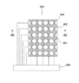
図1は、本発明の第1実施形態に係るタッチパネル付液晶表示装置100について示す図である。この図に示されるように、タッチパネル付液晶表示装置100は、タッチパネル付液晶表示パネル200と、タッチパネル付液晶表示パネル200を挟むように固定する上フレーム101及び下フレーム102と、により構成されている。
FIG. 1 is a diagram showing a liquid
図2は、図1のタッチパネル付液晶表示パネル200の制御構成について示すブロック図である。この図に示されるように、タッチパネル付液晶表示パネル200は、画面表示を行なう液晶表示機能について制御する表示制御部252と、画面へのタッチ位置を検出するタッチパネル機能を制御するタッチパネル制御部254と、表示制御部252及びタッチパネル制御部254を統合的に制御するシステム制御部256と、により制御されている。
FIG. 2 is a block diagram showing a control configuration of the liquid
図3は、図2のタッチパネル制御部254により制御される電極の配置について示す図である。液晶表示に使用される共通電極は、これらが表示領域の全面を覆うように配置されるが、一部はタッチパネル機能の駆動電極としても機能させるために、表示領域の短辺方向に延びる短冊形状の第1電極213及び第2電極215とし、これらを敷き詰めるように配置し、共通電極としている。また、第1電極213は、タッチパネル機能の駆動電極として機能するため、タッチパネル制御部254から電圧が印加される。一方、検出電極222は、長辺方向に延びる短冊形状であり、表示領域の短辺方向に複数並置されており、検出電極222で検出された信号はタッチパネル制御部254に入力される。本実施形態では、隣り合う第1電極213の間には第2電極215が2つ配置されているが、これらの2つ並んだ第2電極215は一体化されて1つとなっていてもよいし、3つ以上並べられた構成となっていてもよい。
FIG. 3 is a diagram showing the arrangement of electrodes controlled by the touch
図4には、図3のIV−IV線における断面図が概略的に示されている。この図に示されるように、タッチパネル付液晶表示パネル200は、不図示の薄膜トランジスタ(TFT:Thin Film Transistor)が形成され、画素毎に液晶の配向を制御するための回路が形成されたTFT基板210と、入射した光を不図示のカラーフィルタにより画素毎にRGB各色の波長の光として出射するカラーフィルタ基板220と、これらの基板の間にシール材232により封止された液晶組成物からなる液晶層231とにより構成されている。
FIG. 4 schematically shows a cross-sectional view taken along line IV-IV in FIG. As shown in this figure, a liquid crystal display panel with a
ここで、TFT基板210には、図4に示されるように、ガラス基板211上に画素電極212並びに液晶表示における共通電極として機能する第1電極213及び第2電極215が形成されており、カラーフィルタ基板220には、ガラス基板221上に検出電極222が形成されている。
Here, as shown in FIG. 4, the
次に、本発明のタッチパネル付液晶表示パネル200の検出原理について説明する。図5には、画面上に指等によるタッチが発生していない場合の電界の様子が示されている。この図に示されるように、タッチパネル制御部254から、所定時間毎に第1電極213にはパルス信号541が入力され、これにより発生する電界により検出電極222には過渡的に電流が流れる。この電流はそれぞれの検出電極222毎にタッチパネル制御部254内の検出回路542により測定される。図6には、画面上で指502等によるタッチが発生している場合の電界の様子が示されている。この図に示されるようにタッチが発生している場合には、電界が遮断され検出電極222を流れる過渡的な電流は減少し、対応する検出回路542での信号レベルが変化するため、タッチパネル制御部254においてタッチを検出することができる。図7は、図5のタッチが発生していない状態と、図6のタッチが発生している状態における検出信号の変化の様子を示すグラフである。なお、検出回路542は、電流を検出するものであっても、電圧を検出するものであってもよい。
Next, the detection principle of the liquid
図8は、第1電極213、第2電極215及び検出電極222の配置について、一部を拡大して示す図である。この図に示されるように、本実施形態では、駆動電極として機能する第1電極213と検出電極222とが交差する面積を小さくすることができるため、過渡電流を少なくすることができ、消費電力を抑えることができると共に、タッチされていない状態のオフセット電流が小さくなることから、より高感度の検出を行なうことができる。
FIG. 8 is an enlarged view showing a part of the arrangement of the
ここで、上述したように、第1電極213及び第2電極215は、液晶表示における共通電極として機能するが、検出は、画素電極212に階調値に基づく電圧を印加したのち、画素電極212がフローティングであるときに行なわれるため、第1電極213及び第2電極215と画素電極212との間の電位差は、第1電極213及び第2電極215の電位が変化したとしても保たれ、原則として画質に影響を与えない。しかしながら、第1電極213及び第2電極215の電位差が大きい場合には、液晶層の電界に影響を与えることも考えられるため、第2電極215にも画質を保持するための電位を印加するようにしている。当該電位は、第1電極213と異なる電位であれば、同じタイミングであってもよいし、それ以外のタイミングであってもよい。例えば、第1電極213より絶対値の小さな電位を印加することにより過渡電流を小さくすることができる。本実施形態では、図8に示されるように、表示制御部252からのパルス信号521を印加するものとしているが、タッチパネル制御部254により印加されることとしてもよい。
Here, as described above, the
[第2実施形態]
図9には、第2実施形態に係るタッチパネル付液晶表示装置の第1電極313、第2電極315及び検出電極222の配置について、一部を拡大して示す図である。この図に示されるように、第2実施形態では、第1実施形態と比較して、第1電極及び第2電極の形状が異なっている。第1電極313は、検出電極222と交差する部分のみ細くなっており、他の部分では広い面積を占めている。このような形状とすることにより、第1電極313と検出電極222との交差部分の面積が小さいため、パルス信号541を印加したときの過渡電流を小さくし、消費電力が抑えることができる。また、オフセット電流が小さくなることから高感度の検出をすることができる。更に、交差部分以外の部分では広い面積を占めているため、広い範囲で画素電極との電位差を保持し、画質を維持することができる。第2電極315は、第1電極313の形状により隙間となる部分を埋めるような形状となっており、第1実施形態と同様にパルス信号521が印加されている。
[Second Embodiment]
FIG. 9 is an enlarged view showing a part of the arrangement of the
[第3実施形態]
図10には、第3実施形態に係るタッチパネル付液晶表示装置の第1電極413、第2電極415及び検出電極222の配置について、一部を拡大して示す図である。この図に示されるように、第3実施形態では、第2実施形態と比較して、第1電極413の検出電極222と交差する位置が異なっている。このような形状とした場合であっても、第1電極413は、検出電極222と交差する部分のみが細くなっているため、第1電極313と検出電極222との交差部分の面積が小さく、パルス信号541を印加したときの過渡電流を小さくし、消費電力が抑えられ、また、オフセット電流が小さくなることから高感度の検出をすることができる。更に、交差部分以外の部分では広い面積を占めているため、広い範囲で画素電極との電位差を保持し、表示画質を維持することができる。また、第2電極415は、第1電極413の形状により隙間となる部分を埋めるような形状となっており、第1実施形態と同様にパルス信号521が印加されている。
[Third Embodiment]
FIG. 10 is an enlarged view showing a part of the arrangement of the
以上説明したように、上述の各実施形態によれば、表示装置の電極をタッチパネルの駆動電極とするタッチパネル付表示装置において、より高感度で消費電力を抑えたタッチパネル付表示装置とすることができる。 As described above, according to the above-described embodiments, in a display device with a touch panel in which the electrode of the display device is a drive electrode of the touch panel, a display device with a touch panel with higher sensitivity and reduced power consumption can be obtained. .
100 タッチパネル付液晶表示装置、101 上フレーム、102 下フレーム、200 タッチパネル付液晶表示パネル、210 TFT基板、211 ガラス基板、212 画素電極、213 第1電極、215 第2電極、220 カラーフィルタ基板、221 ガラス基板、222 検出電極、231 液晶層、232 シール材、252 表示制御部、254 タッチパネル制御部、256 システム制御部、313 第1電極、315 第2電極、413 第1電極、415 第2電極、521 パルス信号、541 パルス信号、542 検出回路。 100 liquid crystal display device with touch panel, 101 upper frame, 102 lower frame, 200 liquid crystal display panel with touch panel, 210 TFT substrate, 211 glass substrate, 212 pixel electrode, 213 first electrode, 215 second electrode, 220 color filter substrate, 221 Glass substrate, 222 detection electrode, 231 liquid crystal layer, 232 sealing material, 252 display control unit, 254 touch panel control unit, 256 system control unit, 313 first electrode, 315 second electrode, 413 first electrode, 415 second electrode, 521 Pulse signal, 541 Pulse signal, 542 Detection circuit.
Claims (5)
前記表示領域を横切るように一方向に延びる複数の電極である共通電極と、
前記表示領域を横切るように、前記一方向とは異なる方向に延び、パネル上の接触位置を検出する複数の電極である検出電極と、
前記画素電極及び前記共通電極により形成される電界により、配向が変化する液晶組成物からなる液晶層と、を備え、
前記共通電極は、
パネル上の接触位置を検出させるための検出期間に、検出電位が印加される第1電極と、
前記検出期間に、前記検出電位とは異なる電位が印加される第2電極と、を有する、ことを特徴とするタッチパネル付液晶表示装置。 A pixel electrode that is a plurality of electrodes that are arranged in each pixel arranged in the display area and to which a potential according to a gradation value is applied;
A common electrode that is a plurality of electrodes extending in one direction so as to cross the display area;
A detection electrode that extends in a direction different from the one direction so as to cross the display area and is a plurality of electrodes that detect a contact position on the panel;
A liquid crystal layer composed of a liquid crystal composition whose orientation is changed by an electric field formed by the pixel electrode and the common electrode,
The common electrode is
A first electrode to which a detection potential is applied in a detection period for detecting a contact position on the panel;
A liquid crystal display device with a touch panel, comprising: a second electrode to which a potential different from the detection potential is applied during the detection period.
前記第1電極は、前記検出電極と交差する交差部と、前記交差しない部分である検出部とを有し、
前記交差部は、検出部と比較して線幅が狭い、ことを特徴とするタッチパネル付液晶表示装置。 A liquid crystal display device with a touch panel according to claim 1,
The first electrode has an intersection that intersects with the detection electrode and a detection portion that is the portion that does not intersect,
The liquid crystal display device with a touch panel, wherein the crossing portion has a narrower line width than the detection portion.
前記第1電極が前記検出電極と重なっていない領域には、前記第2電極が重なるように配置されている、ことを特徴とするタッチパネル付液晶表示装置。 A liquid crystal display device with a touch panel according to claim 1 or 2,
A liquid crystal display device with a touch panel, wherein the second electrode is disposed so as to overlap with a region where the first electrode does not overlap with the detection electrode.
前記第1電極及び前記第2電極は、それぞれ、複数設けられ、
隣り合う2本の前記第1電極の間には、複数本の前記第2電極が配置されていることを特徴とするタッチパネル付液晶表示装置。 A liquid crystal display device with a touch panel according to claim 1,
A plurality of the first electrode and the second electrode are provided,
A liquid crystal display device with a touch panel, wherein a plurality of the second electrodes are arranged between two adjacent first electrodes.
前記第2電極に印加される前記電位は、パルス信号であり、
前記第1電極に前記検出電位が印加されるのと同じタイミングで、前記パルス信号が前記第2電極に印加されることを特徴とするタッチパネル付液晶表示装置。 A liquid crystal display device with a touch panel according to claim 1,
The potential applied to the second electrode is a pulse signal;
The liquid crystal display device with a touch panel, wherein the pulse signal is applied to the second electrode at the same timing as the detection potential is applied to the first electrode.
Priority Applications (2)
| Application Number | Priority Date | Filing Date | Title |
|---|---|---|---|
| JP2012025985A JP5905730B2 (en) | 2012-02-09 | 2012-02-09 | Liquid crystal display with touch panel |
| US13/758,312 US9104259B2 (en) | 2012-02-09 | 2013-02-04 | Liquid crystal display device with touch panel |
Applications Claiming Priority (1)
| Application Number | Priority Date | Filing Date | Title |
|---|---|---|---|
| JP2012025985A JP5905730B2 (en) | 2012-02-09 | 2012-02-09 | Liquid crystal display with touch panel |
Publications (3)
| Publication Number | Publication Date |
|---|---|
| JP2013164649A JP2013164649A (en) | 2013-08-22 |
| JP2013164649A5 JP2013164649A5 (en) | 2015-03-19 |
| JP5905730B2 true JP5905730B2 (en) | 2016-04-20 |
Family
ID=48945183
Family Applications (1)
| Application Number | Title | Priority Date | Filing Date |
|---|---|---|---|
| JP2012025985A Active JP5905730B2 (en) | 2012-02-09 | 2012-02-09 | Liquid crystal display with touch panel |
Country Status (2)
| Country | Link |
|---|---|
| US (1) | US9104259B2 (en) |
| JP (1) | JP5905730B2 (en) |
Families Citing this family (5)
| Publication number | Priority date | Publication date | Assignee | Title |
|---|---|---|---|---|
| US9645431B2 (en) * | 2008-03-19 | 2017-05-09 | Egalax_Empia Technology Inc. | Touch display and method for driving a plurality of touch driving electrodes of touch display |
| WO2014045603A1 (en) * | 2012-09-24 | 2014-03-27 | パナソニック株式会社 | Input device |
| TWI636300B (en) * | 2013-11-15 | 2018-09-21 | 禾瑞亞科技股份有限公司 | Touch display and method for driving a plurality of touch driving electrodes of touch display |
| JP2016004281A (en) * | 2014-06-13 | 2016-01-12 | 株式会社ジャパンディスプレイ | Display device with sensor |
| CN108681122B (en) * | 2018-05-16 | 2020-11-06 | 深圳市华星光电技术有限公司 | In-plane switching display panel and display device |
Family Cites Families (5)
| Publication number | Priority date | Publication date | Assignee | Title |
|---|---|---|---|---|
| JP4744518B2 (en) * | 2005-06-09 | 2011-08-10 | シャープ株式会社 | Liquid crystal display |
| US8040480B2 (en) * | 2008-03-04 | 2011-10-18 | Stanley Electric Co., Ltd. | Liquid crystal display apparatus |
| JP4816668B2 (en) | 2008-03-28 | 2011-11-16 | ソニー株式会社 | Display device with touch sensor |
| US7995041B2 (en) * | 2009-02-02 | 2011-08-09 | Apple Inc. | Integrated touch screen |
| US20130063404A1 (en) * | 2011-09-13 | 2013-03-14 | Abbas Jamshidi Roudbari | Driver Circuitry for Displays |
-
2012
- 2012-02-09 JP JP2012025985A patent/JP5905730B2/en active Active
-
2013
- 2013-02-04 US US13/758,312 patent/US9104259B2/en active Active
Also Published As
| Publication number | Publication date |
|---|---|
| JP2013164649A (en) | 2013-08-22 |
| US20130207914A1 (en) | 2013-08-15 |
| US9104259B2 (en) | 2015-08-11 |
Similar Documents
| Publication | Publication Date | Title |
|---|---|---|
| US10365745B2 (en) | Display device with touch detection function, touch detection device, and electronic unit | |
| JP5513308B2 (en) | Display device with touch detection function and electronic device | |
| US9791991B2 (en) | Display device with a built-in touch panel | |
| KR101929427B1 (en) | Display device including touch sensor | |
| JP6020571B2 (en) | Liquid crystal display | |
| KR101838755B1 (en) | Display device with touch detection funcion, and electronic unit | |
| JP5616184B2 (en) | Display device with touch detection function and electronic device | |
| TWI461792B (en) | Liquid crystal display with built-in touch screen panel | |
| JP5673782B1 (en) | Liquid crystal display | |
| KR101546049B1 (en) | Touch display panel and driving method thereof | |
| US20150192814A1 (en) | Liquid crystal display device | |
| US20160188071A1 (en) | Capacitive in-cell touch panel and display device | |
| TW201818220A (en) | Touch-type display panel and short-repair method thereof | |
| US20150103048A1 (en) | Display device | |
| JP2015072549A (en) | Liquid crystal display device with touch panel | |
| JP5905730B2 (en) | Liquid crystal display with touch panel | |
| US20150153767A1 (en) | Display device | |
| JP6131123B2 (en) | Display device with touch panel | |
| JP2014021865A (en) | Touch panel-equipped liquid crystal display device and manufacturing method for touch panel-equipped liquid crystal display device | |
| JP2023098932A (en) | Display device | |
| US20150160763A1 (en) | Input device and liquid crystal display device | |
| JP5818932B2 (en) | Display device with touch detection function and electronic device | |
| US8866779B2 (en) | Display device | |
| JP2020095106A (en) | Display |
Legal Events
| Date | Code | Title | Description |
|---|---|---|---|
| A521 | Request for written amendment filed |
Free format text: JAPANESE INTERMEDIATE CODE: A523 Effective date: 20150203 |
|
| A621 | Written request for application examination |
Free format text: JAPANESE INTERMEDIATE CODE: A621 Effective date: 20150203 |
|
| A977 | Report on retrieval |
Free format text: JAPANESE INTERMEDIATE CODE: A971007 Effective date: 20151224 |
|
| A131 | Notification of reasons for refusal |
Free format text: JAPANESE INTERMEDIATE CODE: A131 Effective date: 20160105 |
|
| A521 | Request for written amendment filed |
Free format text: JAPANESE INTERMEDIATE CODE: A523 Effective date: 20160202 |
|
| TRDD | Decision of grant or rejection written | ||
| A01 | Written decision to grant a patent or to grant a registration (utility model) |
Free format text: JAPANESE INTERMEDIATE CODE: A01 Effective date: 20160223 |
|
| A61 | First payment of annual fees (during grant procedure) |
Free format text: JAPANESE INTERMEDIATE CODE: A61 Effective date: 20160317 |
|
| R150 | Certificate of patent or registration of utility model |
Ref document number: 5905730 Country of ref document: JP Free format text: JAPANESE INTERMEDIATE CODE: R150 |
|
| R250 | Receipt of annual fees |
Free format text: JAPANESE INTERMEDIATE CODE: R250 |
|
| R250 | Receipt of annual fees |
Free format text: JAPANESE INTERMEDIATE CODE: R250 |
|
| R250 | Receipt of annual fees |
Free format text: JAPANESE INTERMEDIATE CODE: R250 |
|
| R250 | Receipt of annual fees |
Free format text: JAPANESE INTERMEDIATE CODE: R250 |
|
| R250 | Receipt of annual fees |
Free format text: JAPANESE INTERMEDIATE CODE: R250 |
|
| R250 | Receipt of annual fees |
Free format text: JAPANESE INTERMEDIATE CODE: R250 |