JP6255179B2 - 表示装置 - Google Patents
表示装置 Download PDFInfo
- Publication number
- JP6255179B2 JP6255179B2 JP2013144385A JP2013144385A JP6255179B2 JP 6255179 B2 JP6255179 B2 JP 6255179B2 JP 2013144385 A JP2013144385 A JP 2013144385A JP 2013144385 A JP2013144385 A JP 2013144385A JP 6255179 B2 JP6255179 B2 JP 6255179B2
- Authority
- JP
- Japan
- Prior art keywords
- electrode
- electrodes
- display device
- period
- touch
- Prior art date
- Legal status (The legal status is an assumption and is not a legal conclusion. Google has not performed a legal analysis and makes no representation as to the accuracy of the status listed.)
- Active
Links
- 238000001514 detection method Methods 0.000 claims description 48
- 239000000758 substrate Substances 0.000 claims description 29
- 239000004973 liquid crystal related substance Substances 0.000 claims description 25
- 238000012937 correction Methods 0.000 claims description 23
- 230000008859 change Effects 0.000 claims description 10
- 230000005484 gravity Effects 0.000 claims description 5
- 230000002093 peripheral effect Effects 0.000 claims description 3
- 238000006243 chemical reaction Methods 0.000 description 39
- 230000035945 sensitivity Effects 0.000 description 20
- 238000010586 diagram Methods 0.000 description 19
- 230000000052 comparative effect Effects 0.000 description 18
- 230000005540 biological transmission Effects 0.000 description 11
- 230000008878 coupling Effects 0.000 description 8
- 238000010168 coupling process Methods 0.000 description 8
- 238000005859 coupling reaction Methods 0.000 description 8
- 230000009467 reduction Effects 0.000 description 8
- 230000010354 integration Effects 0.000 description 7
- 239000000203 mixture Substances 0.000 description 5
- 230000007423 decrease Effects 0.000 description 4
- 230000006870 function Effects 0.000 description 4
- 239000003990 capacitor Substances 0.000 description 3
- 239000004020 conductor Substances 0.000 description 2
- 239000010410 layer Substances 0.000 description 2
- 238000000034 method Methods 0.000 description 2
- 230000004044 response Effects 0.000 description 2
- 239000003566 sealing material Substances 0.000 description 2
- 238000013459 approach Methods 0.000 description 1
- 230000005684 electric field Effects 0.000 description 1
- 239000011521 glass Substances 0.000 description 1
- 230000006872 improvement Effects 0.000 description 1
- 239000011159 matrix material Substances 0.000 description 1
- 238000005259 measurement Methods 0.000 description 1
- 238000012986 modification Methods 0.000 description 1
- 230000004048 modification Effects 0.000 description 1
- 239000011241 protective layer Substances 0.000 description 1
Images


Classifications
-
- G—PHYSICS
- G06—COMPUTING; CALCULATING OR COUNTING
- G06F—ELECTRIC DIGITAL DATA PROCESSING
- G06F3/00—Input arrangements for transferring data to be processed into a form capable of being handled by the computer; Output arrangements for transferring data from processing unit to output unit, e.g. interface arrangements
- G06F3/01—Input arrangements or combined input and output arrangements for interaction between user and computer
- G06F3/03—Arrangements for converting the position or the displacement of a member into a coded form
- G06F3/041—Digitisers, e.g. for touch screens or touch pads, characterised by the transducing means
- G06F3/044—Digitisers, e.g. for touch screens or touch pads, characterised by the transducing means by capacitive means
- G06F3/0443—Digitisers, e.g. for touch screens or touch pads, characterised by the transducing means by capacitive means using a single layer of sensing electrodes
-
- G—PHYSICS
- G06—COMPUTING; CALCULATING OR COUNTING
- G06F—ELECTRIC DIGITAL DATA PROCESSING
- G06F3/00—Input arrangements for transferring data to be processed into a form capable of being handled by the computer; Output arrangements for transferring data from processing unit to output unit, e.g. interface arrangements
- G06F3/01—Input arrangements or combined input and output arrangements for interaction between user and computer
- G06F3/03—Arrangements for converting the position or the displacement of a member into a coded form
- G06F3/041—Digitisers, e.g. for touch screens or touch pads, characterised by the transducing means
- G06F3/0412—Digitisers structurally integrated in a display
-
- G—PHYSICS
- G06—COMPUTING; CALCULATING OR COUNTING
- G06F—ELECTRIC DIGITAL DATA PROCESSING
- G06F3/00—Input arrangements for transferring data to be processed into a form capable of being handled by the computer; Output arrangements for transferring data from processing unit to output unit, e.g. interface arrangements
- G06F3/01—Input arrangements or combined input and output arrangements for interaction between user and computer
- G06F3/03—Arrangements for converting the position or the displacement of a member into a coded form
- G06F3/041—Digitisers, e.g. for touch screens or touch pads, characterised by the transducing means
- G06F3/0416—Control or interface arrangements specially adapted for digitisers
- G06F3/0418—Control or interface arrangements specially adapted for digitisers for error correction or compensation, e.g. based on parallax, calibration or alignment
-
- G—PHYSICS
- G06—COMPUTING; CALCULATING OR COUNTING
- G06F—ELECTRIC DIGITAL DATA PROCESSING
- G06F3/00—Input arrangements for transferring data to be processed into a form capable of being handled by the computer; Output arrangements for transferring data from processing unit to output unit, e.g. interface arrangements
- G06F3/01—Input arrangements or combined input and output arrangements for interaction between user and computer
- G06F3/03—Arrangements for converting the position or the displacement of a member into a coded form
- G06F3/041—Digitisers, e.g. for touch screens or touch pads, characterised by the transducing means
- G06F3/044—Digitisers, e.g. for touch screens or touch pads, characterised by the transducing means by capacitive means
- G06F3/0445—Digitisers, e.g. for touch screens or touch pads, characterised by the transducing means by capacitive means using two or more layers of sensing electrodes, e.g. using two layers of electrodes separated by a dielectric layer
-
- G—PHYSICS
- G06—COMPUTING; CALCULATING OR COUNTING
- G06F—ELECTRIC DIGITAL DATA PROCESSING
- G06F3/00—Input arrangements for transferring data to be processed into a form capable of being handled by the computer; Output arrangements for transferring data from processing unit to output unit, e.g. interface arrangements
- G06F3/01—Input arrangements or combined input and output arrangements for interaction between user and computer
- G06F3/03—Arrangements for converting the position or the displacement of a member into a coded form
- G06F3/041—Digitisers, e.g. for touch screens or touch pads, characterised by the transducing means
- G06F3/044—Digitisers, e.g. for touch screens or touch pads, characterised by the transducing means by capacitive means
- G06F3/0446—Digitisers, e.g. for touch screens or touch pads, characterised by the transducing means by capacitive means using a grid-like structure of electrodes in at least two directions, e.g. using row and column electrodes
Description
すなわち、静電容量結合方式タッチパネルでは、パネル表示部の中心部に比べてパネル表示部の端近傍において、タッチ位置の検出座標精度が劣る。
すなわち、表示装置は、タッチパネル検出電極において、パネル表示部の端の電極の周期を小さくする。
端の電極周期縮小により座標精度が改善する理由は、パネル端近傍へのタッチに対して端の電極1本のみで反応する領域が小さくなり、複数本の電極が反応するためである。これについて説明する。
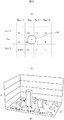
これを図7Aから図7Cでもう少し詳しく見る。図7Aは比較例1に係るパネルの端(x=0)をタッチしたときの反応を示す図である。図7A(a)はパネルのタッチ位置を、図7A(b)は反応値を示している。図7A(a)に示すように疑似指FFの中心はパネルの端(x=0)に位置する。図7A(b)に示すように、x=0の位置では、電極RxNの交点しか反応していない。図7Bは比較例1に係るパネルの端からr/2の位置(x=r/2)をタッチしたときの反応を示す図である。図7B(a)はパネルのタッチ位置を、図7B(b)は反応値を示している。図7B(a)に示すように、疑似指FFの中心はパネルの端(x=r/2)に位置する。図7B(b)に示すように、x=r/2の位置で交点3に少し反応が現れるが、まだノイズと大差ないレベルのため、座標計算に寄与しない。その結果、パネル端ではx=0からx=r/2の位置までRxNの1本のみで反応しているため、x方向の位置の違いが検出できない。即ち、タッチ位置がx=0からx=r/2までの間、検出座標の位置が変わらない。これがパネル端で座標精度が劣化する原因である。図7Cは比較例1に係るパネルの端からrの位置(x=r)をタッチしたときの反応を示す図である。図7C(a)はパネルのタッチ位置を、図7C(b)は反応値を示している。図7C(a)に示すように、疑似指FFの中心はパネルの端(x=r)に位置する。図7C(b)に示すように、x=rでは交点3の反応値が十分大きくなり、座標計算に寄与している。
周期変更により端電極の感度が変わるため、座標計算時にソフトウェアで感度を補正する。Tx−Rx交点の感度は、概算では、その交点の領域面積(Tx周期×Rx周期)に比例する。そのため、端のTx電極と端のRx電極の周期を縮小した場合に、最も感度が低下するのは4隅(コーナー)の交点である。ソフトウェアで感度を補正してもノイズは補正できないので、この4隅の交点でS/N比を確保することが必要であり、この条件により周期縮小の限界が決まる。
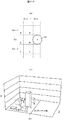
図10Aは比較例1に係る外周座標補正を説明する図である。X方向の電極周期をPxとすると、通常パターン(比較例1)においては、重心計算での各交点の周期もPxとなる。X方向の全体の電極幅をLとすると、単純重心計算でのタッチ座標の取り得る範囲はPx/2〜L−Px/2となる。そこで、Px/2〜Pxの座標を0〜Pxに、L−Px〜L−Px/2の座標をL−Px〜Lに変換する補正を行う。この補正を端補正または外周座標補正という。
周期縮小により端でのキャリブレーション値が変わるため、各Tx−Rx交点毎にキャリブレーションを行う。
先ず、キャリブレーションについて説明する。タッチ検出回路の基本構成(キャブレーション回路なし)例を図11に示す。また、タッチ検出の波形の例を図12に示す。図12(a)はTxパルスの電圧波形を、図12(b)は結合電流の電流波形を、図12(c)は積分出力の電圧波形を、図12(d)は図12(c)を拡大した積分出力の電圧波形を示す。タッチ検出回路51は、積分回路52とアナログ/デジタル変換回路(A/D変換回路、A/D Converter)53を有する。積分回路52は、演算増幅器54と積分容量Cintと参照電圧源Vrefを有する。Tx電極にTxパルスが印加されるとRx電極にTx−Rxの結合容量Cxyに基づくパルス状の結合電流が流れる。この結合電流を積分回路52で電圧に変換する。積分回路52の出力(積分出力)をA/D変換回路53でデジタル値に変換する。タッチによりTx−Rxの結合容量Cxyが変化することでタッチを検出する。
211、217・・・端のTx電極
31・・・検出電極(受信側電極、Rx電極)
311、315・・・端のRx電極
PRx・・・Rx電極の周期
PRxe・・・端のRx電極の周期
PTx・・・Tx電極の周期
PTxe・・・端のTx電極の周期
Claims (14)
- 表示装置は、
所定周期で第1方向に延在する複数の第1電極と、
所定周期で第2方向に延在する複数の第2電極と、
を有し、
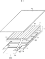
前記複数の第1電極と前記複数の第2電極は、平面視で重なって、断面視で離れて配置され、
前記複数の第1電極のうち両端に位置する第1電極の周期は、他の第1電極の周期よりも小さくするようにされ、
前記複数の第2電極のうち両端に位置する第2電極の周期は、他の第2電極の周期よりも小さくするようにされ、
前記第1電極の周期は、各電極の幅で、
前記第2電極の周期は、前記複数の第2電極のうち、両端に位置する第2電極以外の第2電極では、隣合う電極との間隔の中心線間の距離であり、両端に位置する第2電極では、隣合う電極との間隔の中心線から前記第1電極の端部までであり、
前記複数の第1電極と前記複数の第2電極が交差する箇所の容量変化に基づいてタッチを検出するようにされ、
前記両端に位置する第2電極の中心線は、前記両端に位置する第2電極の周期の中心線より、前記第1電極の端部側にずれていて、前記両端に位置する第2電極の幅は、他の第2電極の幅と同じである。 - 請求項1の表示装置は、
前記複数の第1の電極の両端および前記複数の第2の電極の両端のタッチ反応値を補正して重心計算によりタッチ検出座標を求めるようにされる。 - 請求項2の表示装置は、
前記タッチ検出座標に対して外周座標補正を行うようにされる。 - 請求項1の表示装置は、
前記複数の第1電極と前記複数の第2電極が交差する箇所ごとにキャリブレーションを行うようにされる。 - 請求項1の表示装置において、
前記両端に位置する第1電極の幅は、他の第1電極の幅よりも小さくするようにされ、 前記両端に位置する第2電極の幅は、他の第2電極の幅よりも小さくするようにされる。 - 請求項1の表示装置において、
前記両端に位置する第2電極と前記両端に位置する第2電極に隣接する前記他の第2電極との距離と、隣接する前記他の第2電極間の距離とを同じにするようにされる。 - 請求項1の表示装置において、
前記両端に位置する第2電極と前記両端に位置する第2電極に隣接する前記他の第2電極との距離は、隣接する前記他の第2電極間の距離より小さくするようにされる。 - 請求項1の表示装置において、
さらに画素が形成される第1の基板とカラーフィルタが形成される第2の基板とを有し、
前記複数の第1の電極は、前記第1の基板と前記第2の基板との間に形成される。 - 請求項8の表示装置において、
さらに前記第1の基板と前記第2の基板の間に液晶層を有し、
前記複数の第2の電極は、前記液晶層とは反対側の前記第2の基板上に形成される。 - 請求項1の表示装置において、
前記複数の第1電極と前記複数の第2電極とが平面視で重ならない部分の電極は、ひし形形状であり、
前記両端に位置する第1電極の幅は、他の第1電極の幅よりも小さくするようにされ、
前記両端に位置する第2電極の幅は、他の第2電極の幅よりも小さくするようにされる。 - 請求項10の表示装置において、
さらに画素が形成される表示パネルを有し、
前記複数の第1の電極は、前記表示パネルと前記複数の第2の電極との間に形成される。 - 請求項11の表示装置において、
前記表示パネルは、液晶表示パネルである。 - 請求項1の表示装置において、
前記両端に位置する第2電極の中心線は、前記両端に位置する第2電極の周期の中心線より、前記第1電極の端部側にずれている。 - 請求項1の表示装置において、
前記両端に位置する第2電極の中心線は、前記両端に位置する第2電極の周期の中心線より、前記第1電極の端部側にずれていて、前記両端に位置する第2電極の幅は、他の第2電極の幅よりも小さい。
Priority Applications (4)
| Application Number | Priority Date | Filing Date | Title |
|---|---|---|---|
| JP2013144385A JP6255179B2 (ja) | 2013-07-10 | 2013-07-10 | 表示装置 |
| TW103121102A TWI549045B (zh) | 2013-07-10 | 2014-06-18 | 顯示裝置 |
| US14/325,681 US9841851B2 (en) | 2013-07-10 | 2014-07-08 | Display device |
| US15/803,936 US10444928B2 (en) | 2013-07-10 | 2017-11-06 | Display device |
Applications Claiming Priority (1)
| Application Number | Priority Date | Filing Date | Title |
|---|---|---|---|
| JP2013144385A JP6255179B2 (ja) | 2013-07-10 | 2013-07-10 | 表示装置 |
Publications (3)
| Publication Number | Publication Date |
|---|---|
| JP2015018362A JP2015018362A (ja) | 2015-01-29 |
| JP2015018362A5 JP2015018362A5 (ja) | 2016-08-18 |
| JP6255179B2 true JP6255179B2 (ja) | 2017-12-27 |
Family
ID=52276723
Family Applications (1)
| Application Number | Title | Priority Date | Filing Date |
|---|---|---|---|
| JP2013144385A Active JP6255179B2 (ja) | 2013-07-10 | 2013-07-10 | 表示装置 |
Country Status (3)
| Country | Link |
|---|---|
| US (2) | US9841851B2 (ja) |
| JP (1) | JP6255179B2 (ja) |
| TW (1) | TWI549045B (ja) |
Families Citing this family (14)
| Publication number | Priority date | Publication date | Assignee | Title |
|---|---|---|---|---|
| JP6255179B2 (ja) * | 2013-07-10 | 2017-12-27 | 株式会社ジャパンディスプレイ | 表示装置 |
| KR102276997B1 (ko) * | 2014-10-13 | 2021-07-14 | 삼성디스플레이 주식회사 | 터치 센서를 구비한 표시 장치 |
| TWI575432B (zh) * | 2015-06-12 | 2017-03-21 | 映智科技股份有限公司 | 感測裝置 |
| US10162465B2 (en) * | 2015-07-27 | 2018-12-25 | Parade Technologies, Ltd. | Methods and devices for determining touch locations on a touch-sensitive surface |
| JP6908493B2 (ja) * | 2017-10-11 | 2021-07-28 | ローム株式会社 | タッチパネルの制御回路、制御方法、それを用いたタッチ式入力装置、電子機器 |
| CN108874234B (zh) * | 2018-08-02 | 2022-03-04 | 深圳市德明利技术股份有限公司 | 一种触控识别方法、装置及触控显示装置 |
| CN111488083B (zh) * | 2019-01-25 | 2023-03-31 | 瑞昱半导体股份有限公司 | 具有自校准功能的电容式触摸检测装置 |
| JP6998920B2 (ja) * | 2019-08-06 | 2022-01-18 | 双葉電子工業株式会社 | タッチパネル装置 |
| TWI708173B (zh) * | 2019-08-26 | 2020-10-21 | 友達光電股份有限公司 | 觸控面板 |
| KR20210091544A (ko) * | 2020-01-14 | 2021-07-22 | 에스케이이노베이션 주식회사 | 지문 센서를 포함하는 터치 디스플레이 장치 |
| KR20210091546A (ko) | 2020-01-14 | 2021-07-22 | 에스케이이노베이션 주식회사 | 지문 센서를 포함하는 터치 센서 |
| CN111816073B (zh) * | 2020-07-06 | 2023-04-25 | 京东方科技集团股份有限公司 | 显示模组、显示装置以及显示模组的校准方法 |
| WO2023069088A1 (en) * | 2021-10-20 | 2023-04-27 | Google Llc | Touch coordinate edge correction |
| TW202326380A (zh) * | 2021-12-22 | 2023-07-01 | 禾瑞亞科技股份有限公司 | 觸控螢幕及其觸控處理裝置和方法 |
Family Cites Families (25)
| Publication number | Priority date | Publication date | Assignee | Title |
|---|---|---|---|---|
| US5565658A (en) * | 1992-07-13 | 1996-10-15 | Cirque Corporation | Capacitance-based proximity with interference rejection apparatus and methods |
| JP3582393B2 (ja) * | 1999-02-09 | 2004-10-27 | セイコーエプソン株式会社 | デバイス制御装置、ユーザインターフェイス表示方法およびユーザインターフェイスを表示させるためのコンピュータプログラムを記録した記録媒体 |
| US7030860B1 (en) | 1999-10-08 | 2006-04-18 | Synaptics Incorporated | Flexible transparent touch sensing system for electronic devices |
| TWI374379B (en) * | 2007-12-24 | 2012-10-11 | Wintek Corp | Transparent capacitive touch panel and manufacturing method thereof |
| JP4816668B2 (ja) * | 2008-03-28 | 2011-11-16 | ソニー株式会社 | タッチセンサ付き表示装置 |
| KR101080183B1 (ko) * | 2008-04-04 | 2011-11-07 | (주)멜파스 | 가장자리 위치 인식 특성이 개선된 접촉 감지 장치 |
| TWI371709B (en) * | 2008-07-07 | 2012-09-01 | Wintek Corp | Touch device and touch display apparatus |
| KR101577952B1 (ko) * | 2009-03-10 | 2015-12-17 | 삼성디스플레이 주식회사 | 터치 패널 장치 |
| TWI379226B (en) * | 2009-03-13 | 2012-12-11 | Tpk Touch Solutions Inc | Liquid crystal display with integrated capacitive touch device |
| JP5219965B2 (ja) * | 2009-08-27 | 2013-06-26 | 株式会社ジャパンディスプレイイースト | タッチパネル装置 |
| US20110181519A1 (en) * | 2010-01-26 | 2011-07-28 | Himax Technologies Limited | System and method of driving a touch screen |
| US8797281B2 (en) * | 2010-06-16 | 2014-08-05 | Atmel Corporation | Touch-screen panel with multiple sense units and related methods |
| KR101733140B1 (ko) * | 2010-09-14 | 2017-05-08 | 삼성디스플레이 주식회사 | 터치스크린패널 일체형 영상표시장치 및 그 제조방법 |
| JP5667824B2 (ja) * | 2010-09-24 | 2015-02-12 | 株式会社ジャパンディスプレイ | タッチ検出装置およびその駆動方法、タッチ検出機能付き表示装置、ならびに電子機器 |
| JP5616184B2 (ja) * | 2010-09-28 | 2014-10-29 | 株式会社ジャパンディスプレイ | タッチ検出機能付き表示装置および電子機器 |
| KR101322998B1 (ko) * | 2010-10-01 | 2013-10-29 | 엘지디스플레이 주식회사 | 정전용량 방식 터치 스크린 패널 |
| TW201218028A (en) * | 2010-10-26 | 2012-05-01 | Novatek Microelectronics Corp | Coordinates algorithm of touch panel |
| TWI403939B (zh) * | 2010-12-31 | 2013-08-01 | Au Optronics Corp | 觸控面板以及觸控顯示面板 |
| JP6092516B2 (ja) * | 2011-01-18 | 2017-03-08 | 富士フイルム株式会社 | 導電性フイルム及びそれを備えた表示装置 |
| JP4897983B1 (ja) * | 2011-05-18 | 2012-03-14 | パナソニック株式会社 | タッチパネル装置および指示物判別方法 |
| US9116581B2 (en) * | 2011-08-24 | 2015-08-25 | Cypress Semiconductor Corporation | Edge accuracy in a capacitive sense array |
| JP2014010671A (ja) * | 2012-06-29 | 2014-01-20 | Mitsubishi Electric Corp | タッチスクリーン、タッチパネル及びそれを備える表示装置 |
| TW201409114A (zh) * | 2012-08-23 | 2014-03-01 | Henghao Technology Co Ltd | 觸控電極裝置 |
| JP5968243B2 (ja) * | 2013-02-07 | 2016-08-10 | 株式会社ジャパンディスプレイ | 入力装置、表示装置および電子機器 |
| JP6255179B2 (ja) * | 2013-07-10 | 2017-12-27 | 株式会社ジャパンディスプレイ | 表示装置 |
-
2013
- 2013-07-10 JP JP2013144385A patent/JP6255179B2/ja active Active
-
2014
- 2014-06-18 TW TW103121102A patent/TWI549045B/zh active
- 2014-07-08 US US14/325,681 patent/US9841851B2/en active Active
-
2017
- 2017-11-06 US US15/803,936 patent/US10444928B2/en active Active
Also Published As
| Publication number | Publication date |
|---|---|
| US10444928B2 (en) | 2019-10-15 |
| TWI549045B (zh) | 2016-09-11 |
| US20150015538A1 (en) | 2015-01-15 |
| US20180059827A1 (en) | 2018-03-01 |
| US9841851B2 (en) | 2017-12-12 |
| JP2015018362A (ja) | 2015-01-29 |
| TW201502942A (zh) | 2015-01-16 |
Similar Documents
| Publication | Publication Date | Title |
|---|---|---|
| JP6255179B2 (ja) | 表示装置 | |
| EP3062201B1 (en) | Touch input device | |
| US8829926B2 (en) | Transparent proximity sensor | |
| TWI465991B (zh) | Display device | |
| JP7190347B2 (ja) | ペンが送信したペン信号を検出するためのセンサ | |
| US9013448B2 (en) | Touch panel system and electronic device | |
| US20140362034A1 (en) | Touch display device | |
| JP2009015492A (ja) | タッチパネル付き表示装置 | |
| US10331256B2 (en) | Method for correcting sensitivity of touch input device that detects touch pressure and computer-readable recording medium | |
| JP7202906B2 (ja) | ペンが送信したペン信号を検出するためのセンサパネル | |
| JP7375094B2 (ja) | センサパネル | |
| CN103513825A (zh) | 触控装置 | |
| US20180210599A1 (en) | Touch pressure sensitivity correction method and computer-readable recording medium | |
| WO2015192597A1 (zh) | 触摸面板及其驱动方法、显示装置 | |
| JP2010117829A (ja) | タッチパネル付き表示装置 | |
| US10627951B2 (en) | Touch-pressure sensitivity correction method and computer-readable recording medium | |
| US20170010729A1 (en) | Detection method for enhanced 3d detection module | |
| US20190302947A1 (en) | Method for correcting sensitivity of touch input device that detects touch pressure and computer-readable recording medium | |
| US20210041985A1 (en) | Touch panel and display device | |
| KR20150081574A (ko) | 고감도 터치스크린 패널 | |
| US9417742B2 (en) | Touch sensitive display | |
| JP2020024592A (ja) | タッチスクリーン、タッチパネル、表示装置、及び、電子機器 | |
| JP2019121330A (ja) | センサパネル | |
| KR20150077850A (ko) | 터치 스크린 장치의 캘리브레이션 방법 및 터치 스크린 장치 |
Legal Events
| Date | Code | Title | Description |
|---|---|---|---|
| A521 | Request for written amendment filed |
Free format text: JAPANESE INTERMEDIATE CODE: A523 Effective date: 20160704 |
|
| A621 | Written request for application examination |
Free format text: JAPANESE INTERMEDIATE CODE: A621 Effective date: 20160704 |
|
| A977 | Report on retrieval |
Free format text: JAPANESE INTERMEDIATE CODE: A971007 Effective date: 20170718 |
|
| A131 | Notification of reasons for refusal |
Free format text: JAPANESE INTERMEDIATE CODE: A131 Effective date: 20170829 |
|
| A521 | Request for written amendment filed |
Free format text: JAPANESE INTERMEDIATE CODE: A523 Effective date: 20171024 |
|
| TRDD | Decision of grant or rejection written | ||
| A01 | Written decision to grant a patent or to grant a registration (utility model) |
Free format text: JAPANESE INTERMEDIATE CODE: A01 Effective date: 20171107 |
|
| A61 | First payment of annual fees (during grant procedure) |
Free format text: JAPANESE INTERMEDIATE CODE: A61 Effective date: 20171204 |
|
| R150 | Certificate of patent or registration of utility model |
Ref document number: 6255179 Country of ref document: JP Free format text: JAPANESE INTERMEDIATE CODE: R150 |
|
| R250 | Receipt of annual fees |
Free format text: JAPANESE INTERMEDIATE CODE: R250 |
|
| R250 | Receipt of annual fees |
Free format text: JAPANESE INTERMEDIATE CODE: R250 |
|
| R250 | Receipt of annual fees |
Free format text: JAPANESE INTERMEDIATE CODE: R250 |
|
| R250 | Receipt of annual fees |
Free format text: JAPANESE INTERMEDIATE CODE: R250 |