JP3813402B2 - 半導体装置の製造方法 - Google Patents
半導体装置の製造方法 Download PDFInfo
- Publication number
- JP3813402B2 JP3813402B2 JP2000021913A JP2000021913A JP3813402B2 JP 3813402 B2 JP3813402 B2 JP 3813402B2 JP 2000021913 A JP2000021913 A JP 2000021913A JP 2000021913 A JP2000021913 A JP 2000021913A JP 3813402 B2 JP3813402 B2 JP 3813402B2
- Authority
- JP
- Japan
- Prior art keywords
- layer
- conductor layer
- wiring pattern
- semiconductor
- forming
- Prior art date
- Legal status (The legal status is an assumption and is not a legal conclusion. Google has not performed a legal analysis and makes no representation as to the accuracy of the status listed.)
- Expired - Fee Related
Links
Images
Classifications
-
- H—ELECTRICITY
- H10—SEMICONDUCTOR DEVICES; ELECTRIC SOLID-STATE DEVICES NOT OTHERWISE PROVIDED FOR
- H10W—GENERIC PACKAGES, INTERCONNECTIONS, CONNECTORS OR OTHER CONSTRUCTIONAL DETAILS OF DEVICES COVERED BY CLASS H10
- H10W74/00—Encapsulations, e.g. protective coatings
- H10W74/10—Encapsulations, e.g. protective coatings characterised by their shape or disposition
- H10W74/111—Encapsulations, e.g. protective coatings characterised by their shape or disposition the semiconductor body being completely enclosed
- H10W74/114—Encapsulations, e.g. protective coatings characterised by their shape or disposition the semiconductor body being completely enclosed by a substrate and the encapsulations
-
- H—ELECTRICITY
- H10—SEMICONDUCTOR DEVICES; ELECTRIC SOLID-STATE DEVICES NOT OTHERWISE PROVIDED FOR
- H10W—GENERIC PACKAGES, INTERCONNECTIONS, CONNECTORS OR OTHER CONSTRUCTIONAL DETAILS OF DEVICES COVERED BY CLASS H10
- H10W70/00—Package substrates; Interposers; Redistribution layers [RDL]
- H10W70/01—Manufacture or treatment
- H10W70/05—Manufacture or treatment of insulating or insulated package substrates, or of interposers, or of redistribution layers
- H10W70/093—Connecting or disconnecting other interconnections thereto or therefrom, e.g. connecting bond wires or bumps
-
- H—ELECTRICITY
- H10—SEMICONDUCTOR DEVICES; ELECTRIC SOLID-STATE DEVICES NOT OTHERWISE PROVIDED FOR
- H10W—GENERIC PACKAGES, INTERCONNECTIONS, CONNECTORS OR OTHER CONSTRUCTIONAL DETAILS OF DEVICES COVERED BY CLASS H10
- H10W70/00—Package substrates; Interposers; Redistribution layers [RDL]
- H10W70/60—Insulating or insulated package substrates; Interposers; Redistribution layers
- H10W70/611—Insulating or insulated package substrates; Interposers; Redistribution layers for connecting multiple chips together
- H10W70/614—Insulating or insulated package substrates; Interposers; Redistribution layers for connecting multiple chips together the multiple chips being integrally enclosed
-
- H—ELECTRICITY
- H10—SEMICONDUCTOR DEVICES; ELECTRIC SOLID-STATE DEVICES NOT OTHERWISE PROVIDED FOR
- H10W—GENERIC PACKAGES, INTERCONNECTIONS, CONNECTORS OR OTHER CONSTRUCTIONAL DETAILS OF DEVICES COVERED BY CLASS H10
- H10W90/00—Package configurations
- H10W90/701—Package configurations characterised by the relative positions of pads or connectors relative to package parts
-
- H—ELECTRICITY
- H10—SEMICONDUCTOR DEVICES; ELECTRIC SOLID-STATE DEVICES NOT OTHERWISE PROVIDED FOR
- H10W—GENERIC PACKAGES, INTERCONNECTIONS, CONNECTORS OR OTHER CONSTRUCTIONAL DETAILS OF DEVICES COVERED BY CLASS H10
- H10W70/00—Package substrates; Interposers; Redistribution layers [RDL]
- H10W70/099—Connecting interconnections to insulating or insulated package substrates, interposers or redistribution layers
-
- H—ELECTRICITY
- H10—SEMICONDUCTOR DEVICES; ELECTRIC SOLID-STATE DEVICES NOT OTHERWISE PROVIDED FOR
- H10W—GENERIC PACKAGES, INTERCONNECTIONS, CONNECTORS OR OTHER CONSTRUCTIONAL DETAILS OF DEVICES COVERED BY CLASS H10
- H10W72/00—Interconnections or connectors in packages
- H10W72/01—Manufacture or treatment
- H10W72/0198—Manufacture or treatment batch processes
-
- H—ELECTRICITY
- H10—SEMICONDUCTOR DEVICES; ELECTRIC SOLID-STATE DEVICES NOT OTHERWISE PROVIDED FOR
- H10W—GENERIC PACKAGES, INTERCONNECTIONS, CONNECTORS OR OTHER CONSTRUCTIONAL DETAILS OF DEVICES COVERED BY CLASS H10
- H10W72/00—Interconnections or connectors in packages
- H10W72/071—Connecting or disconnecting
- H10W72/073—Connecting or disconnecting of die-attach connectors
-
- H—ELECTRICITY
- H10—SEMICONDUCTOR DEVICES; ELECTRIC SOLID-STATE DEVICES NOT OTHERWISE PROVIDED FOR
- H10W—GENERIC PACKAGES, INTERCONNECTIONS, CONNECTORS OR OTHER CONSTRUCTIONAL DETAILS OF DEVICES COVERED BY CLASS H10
- H10W72/00—Interconnections or connectors in packages
- H10W72/851—Dispositions of multiple connectors or interconnections
- H10W72/874—On different surfaces
-
- H—ELECTRICITY
- H10—SEMICONDUCTOR DEVICES; ELECTRIC SOLID-STATE DEVICES NOT OTHERWISE PROVIDED FOR
- H10W—GENERIC PACKAGES, INTERCONNECTIONS, CONNECTORS OR OTHER CONSTRUCTIONAL DETAILS OF DEVICES COVERED BY CLASS H10
- H10W90/00—Package configurations
-
- H—ELECTRICITY
- H10—SEMICONDUCTOR DEVICES; ELECTRIC SOLID-STATE DEVICES NOT OTHERWISE PROVIDED FOR
- H10W—GENERIC PACKAGES, INTERCONNECTIONS, CONNECTORS OR OTHER CONSTRUCTIONAL DETAILS OF DEVICES COVERED BY CLASS H10
- H10W90/00—Package configurations
- H10W90/701—Package configurations characterised by the relative positions of pads or connectors relative to package parts
- H10W90/731—Package configurations characterised by the relative positions of pads or connectors relative to package parts of die-attach connectors
- H10W90/734—Package configurations characterised by the relative positions of pads or connectors relative to package parts of die-attach connectors between a chip and a stacked insulating package substrate, interposer or RDL
Landscapes
- Production Of Multi-Layered Print Wiring Board (AREA)
- Wire Bonding (AREA)
- Structures For Mounting Electric Components On Printed Circuit Boards (AREA)
Description
【発明の属する技術分野】
本発明は、半導体装置の製造方法に関し、特に、パッケージに半導体素子(チップ)を実装してなる半導体装置の高機能化を簡便に行うのに有用な技術に関する。
【0002】
【従来の技術】
パッケージに半導体素子を実装してなる半導体装置として、種々の形態のものが提案されている。その一例として、1枚の基板に複数個の半導体チップを搭載し、高集積化と共に高機能化を意図した半導体装置がある。
かかる半導体装置の具体的な形態としては、例えば、基板の両面にそれぞれ半導体チップを搭載したもの、基板の片面に半導体チップを積み重ねて搭載したもの、基板の平面内に複数個の半導体チップを搭載したもの等が知られている。いずれの形態においても、基板の表面には配線パターンが適宜形成されており、この配線パターンに、各半導体チップの電極パッド(端子)がワイヤボンディングによって電気的に接続されている。もちろん、各半導体チップと配線パターンとの電気的接続はワイヤボンディング接続に限らず、フリップチップ接続やTAB接続等も利用できる。
【0003】
【発明が解決しようとする課題】
上述したように従来の半導体装置では、基板の搭載面内に半導体チップを搭載しているため、基板が規定の大きさに作られることに鑑み、搭載する半導体チップの個数が制限されるといった不利がある。
また、半導体チップを積み重ねて搭載する場合でも、ワイヤボンディング接続のための領域を必要とする分だけ、下側のチップよりも上側のチップの方をサイズ的に小さくする必要があり、そのために上側のチップの搭載面積が狭くなり、チップを積み重ねる個数にも自ずと限界がある。
【0004】
この場合、フリップチップ接続を利用すると、上述したようなボンディングのための領域を設ける必要がないため、ワイヤボンディング接続の場合に比べてチップの搭載数を増やすことが可能であるが、別の不都合が生じる。
一般的に、フリップチップ実装では、半導体チップの電極パッドにはんだ等の金属のバンプ(電極端子)を形成し、このバンプをプリント基板等の実装基板の対応する電極パッド上に熱的に押し付けて接続する。これをチップの積層形態に当てはめると、下側のチップに対し上側のチップがフリップチップ接続されることになる。この場合、上側のチップの電極端子であるバンプの位置に対応するように下側のチップの上面に電極パッドを形成する必要があり、また、チップを積み重ねる際に上側のチップのバンプと下側のチップの電極パッドとの位置合わせを行わなければならず、プロセスが全体的に複雑化するといった不利がある。
【0005】
このように従来の半導体装置では、単に基板の搭載面に半導体チップを搭載しているため、搭載する半導体チップの個数が限定され、必ずしも十分な高機能化等を図ることができないといった課題があった。
また、半導体チップは基板に外付けされた形態で搭載されるため、半導体装置全体としての厚みが相対的に厚くなるといった不利もある。
【0006】
一方、上述した従来形とは別の形態として、更なる高集積化及び高機能化を図るために、基板を多層化し基板内に半導体チップを内蔵する形式の半導体装置が考えられている。例えば、複数の配線層を備えた多層基板の構造を利用すれば、半導体チップを相互に電気的に接続して基板内で3次元的に配置することは可能である。
【0007】
しかしながら、基板内に半導体チップを埋設し、且つ配線層を多層に形成することは必ずしも容易ではなく、また、昨今のパッケージに対する小型化及び軽量化の要求を考慮すると、全体の厚さを薄くして半導体装置をコンパクトに形成しなければならないといった課題もある。
本発明は、上述した従来技術における課題に鑑み創作されたもので、パッケージに半導体素子を実装するに際しコンパクトに構成可能とし、また必要に応じて半導体素子の3次元的な配置構成及び相互間の接続を簡便に行えるようにし、ひいては高機能化に寄与することができる半導体装置の製造方法を提供することを目的とする。
【0008】
【課題を解決するための手段】
上述した従来技術の課題を解決するため、本発明に係る半導体装置の製造方法は、第1の絶縁層の一方の面に配線パターンを含む第1の導体層が形成されてなるベース基板の前記第1の絶縁層の他方の面側に所要の個数の半導体素子を実装する第1の工程と、前記半導体素子を覆うようにして第2の絶縁層を形成し、該第2の絶縁層上に配線パターンを含む第2の導体層を形成する第2の工程と、前記第2の導体層の特定の位置に前記半導体素子の電極端子に達するようにビアホールを形成すると共に、前記半導体素子が埋設されている部分を避ける位置において上下方向に貫通するようにスルーホールを形成する第3の工程と、前記ビアホール及びスルーホールの内壁面を含む表面全体に第3の導体層を形成する第4の工程と、前記半導体素子の電極端子が、前記ビアホールの内壁面の導体層を介して前記第2の導体層に電気的に接続されると共に、前記スルーホールの内壁面の導体層を介して前記第1の導体層に電気的に接続されるように、前記第3の導体層にパターニングを施して配線パターンを形成する第5の工程と、外部接続端子が接続されるべき前記第3の導体層の配線パターンの端子形成部分が露出するように配線パターン、前記第1及び第2の絶縁層を覆って保護膜を形成する第6の工程と、該第6の工程により得られた構造体を、少なくとも1個の半導体素子が含まれるように各パッケージに分割する第7の工程とを含むことを特徴とする。
【0010】
本発明に係る半導体装置の製造方法によれば、パッケージとして供される配線基板内に半導体素子が埋設・実装されているので、半導体装置をコンパクトに構成することができる。
また、配線基板(パッケージ)の両面において配線パターンの端子形成部分を保護膜から露出させ、必要に応じて多層的に積み重ねることができるようにしているので、外部接続端子を介在して半導体素子の3次元的な配置構成及び相互間の接続を簡便に行うことができる。これによって、半導体装置の高機能化を図ることが可能となる。
【0014】
【発明の実施の形態】
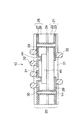
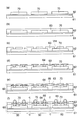
図1は本発明の第1の実施形態に係る半導体装置の断面的な構造を模式的に示したものである。
本実施形態に係る半導体装置10は、パッケージとして供される配線基板20と、このパッケージ(配線基板)20内に埋設・実装された半導体チップ40とによって構成されている。
【0015】
パッケージ(配線基板)20において、21は配線基板のベースとなるベース基板を示し、絶縁層としての樹脂層22の一方の面(図示の例では下側)に導体層としての銅(Cu)箔23が形成された構造を有している。また、24はベース基板21の他方の面(樹脂層22側)の上に形成された接着剤層、25は接着剤層24の上に半導体チップ40を覆うようにして形成された銅箔付き樹脂フィルムを示す。この銅箔付き樹脂フィルム25は、ベース基板21と同様に、絶縁膜としての樹脂フィルム26の一方の面(図示の例では上側)に導体層としての銅箔27が形成された構造を有している。
【0016】
また、VHは銅箔付き樹脂フィルム25の特定の位置において半導体チップ40の電極パッド(端子)に達するように形成されたビアホール、THは半導体チップ40が埋設・実装されていない部分の銅箔付き樹脂フィルム25の特定の位置において基板を上下方向に貫通するように形成されたスルーホール、29はビアホールVH及びスルーホールTHの内壁を含めて銅箔23,27の上に所要形状にパターニングされて形成された配線パターン(導体層)を示す。この配線パターン29は、パッケージ20内に埋設・実装された半導体チップ40の電極パッドが、ビアホールVHの内壁面の導体層29を介して基板の一方の面側の導体層29に電気的に接続されると共に、更にスルーホールTHの内壁面の導体層29を介して基板の他方の面側の導体層29にも電気的に接続されるように、形成されている。
【0017】
また、30はスルーホールTH内に充填された樹脂(絶縁体)、31は配線パターン29、樹脂層22及び樹脂フィルム26を覆って形成された保護膜としてのソルダレジスト層、32は本装置10の外部接続端子として機能するはんだバンプを示す。ソルダレジスト層31は、配線パターン29の端子形成部分(パッド部)に対応する領域に開口部を有するように、つまり配線パターン29の端子形成部分が露出するように、形成されている。そして、この露出した配線パターン29の端子形成部分に、図示のように外部接続端子としてのはんだバンプ32が接合されている。
【0018】
一方、半導体チップ40はパッケージ(配線基板)20内に実装するため、厚さが可及的に薄いものを使用するのが望ましい。現状の技術では、半導体チップとして50μm〜100μm程度の厚さのものが提供されており、この程度の厚さの半導体チップであれば基板内に埋設・実装することは技術的に十分に可能である。本実施形態では、半導体チップ40として厚さが50μm程度の薄いものを使用している。
【0019】
本実施形態に係る半導体装置10は、厚さが50μm程度の薄い半導体チップ40をパッケージ(配線基板)20内に埋設・実装すると共に、パッケージ(配線基板)20の両面に外部接続端子としてのはんだバンプ32を設け、必要に応じて多層的に積み重ねることができるようにしたことを特徴としている。
なお、図1の例示でははんだバンプ(外部接続端子)32を設けているが、これは必ずしも設ける必要はない。要は、はんだバンプ等の外部接続端子が接続可能なように配線パターン29の一部(端子形成部分)がソルダレジスト層31から露出していれば十分である。
【0020】
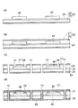
以下、本実施形態の半導体装置10を製造する方法について、その製造工程を順に示す図2及び図3を参照しながら説明する。
先ず最初の工程では(図2(a)参照)、絶縁層としての樹脂層22の一方の面に導体層としての銅箔23が形成されたベース基板21を用意し、このベース基板21の他方の面(樹脂層22側)の上に接着剤を塗布し(接着剤層24)、更にこの接着剤層24の上に所要の個数の半導体チップ40(厚さが50μm程度の薄いもの)を適宜配置し、実装する。半導体チップ40の実装は、当該チップの電極パッド(端子)が形成されている側と反対側の面が接着剤層24に接着されるように行われる。
【0021】
なお、ベース基板21を構成する樹脂層22の材料としては、例えばエポキシ樹脂、ポリイミド樹脂、フェノール樹脂等の熱硬化性樹脂が用いられる。ベース基板21の具体的な形態としては、例えば、ポリイミド樹脂フィルムの表面にポリイミド系の熱可塑性接着剤を塗布し、その上に銅箔を熱プレス接着したものを使用することができる。
【0022】
次の工程では(図2(b)参照)、接着剤層24の上に半導体チップ40を覆うようにして、絶縁膜としての樹脂フィルム26の一方の面に導体層としての銅箔27が形成された銅箔付き樹脂フィルム25を、その樹脂フィルム26側を下にして形成する。樹脂フィルム26の材料としては、上述した樹脂層22と同様に、エポキシ樹脂、ポリイミド樹脂等の熱硬化性樹脂が用いられる。また、銅箔付き樹脂フィルム25の形態については、上述したベース基板21と同様のものを使用することができる。
【0023】
次の工程では(図2(c)参照)、銅箔付き樹脂フィルム25の特定の位置において、各半導体チップ40の電極パッドに達するようにビアホールVHを形成する。また、半導体チップ40が埋設・実装されていない部分の銅箔付き樹脂フィルム25の特定の位置において、基板を上下方向に貫通するようにスルーホールTHを形成する。ビアホールVHの穴明け処理は、先ず特定の位置に対応する銅箔27の部分をエッチングにより除去する工程と、次に樹脂フィルム26の対応する部分をレーザにより除去する工程の2段階からなる。同様に、スルーホールTHの穴明け処理についても、先ず特定の位置に対応する銅箔23,27の部分をエッチングにより除去する工程と、次に樹脂層22及び樹脂フィルム26と接着剤層24の対応する部分をレーザにより除去する工程の2段階からなる。レーザとしては、CO2 レーザやエキシマレーザ等が用いられる。
【0024】
この後、必要に応じて、穴明け処理により樹脂片や汚れ等が生じた場合にこれを除去するための処理(デバリング、デスミア等)を行う。
次の工程では(図2(d)参照)、ビアホールVH及びスルーホールTHの内壁を含めて銅箔23,27の上に、当該銅箔をめっき給電層としてCuの電解めっきを施し、導体層(Cu層)28を形成する。
【0025】
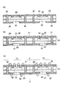
次の工程では(図3(a)参照)、導体層28にパターニングを施して配線パターン(Cu層)29を形成し、また、スルーホールTH内にエポキシ樹脂等の熱硬化性樹脂(絶縁体30)を充填する。導体層28のパターニングは、埋設・実装された半導体チップ40の電極パッドが、ビアホールVHの内壁面の導体層を介して基板の一方の面側の導体層に電気的に接続されると共に、更にスルーホールTHの内壁面の導体層を介して基板の他方の面側の導体層にも電気的に接続されるように、配線パターン29の形状に応じたマスク(図示せず)を用いて行われる。この際、銅箔23,27の露出部分も、同じマスクを用いてエッチングにより除去される。
【0026】
次の工程では(図3(b)参照)、配線パターン29、樹脂層22及び樹脂フィルム26の上に感光性のソルダレジストを塗布し、更に配線パターン29の端子形成部分(パッド部)の形状に従うように露光及び現像(ソルダレジストのパターニング)を行い、その端子形成部分の領域に対応する部分のソルダレジスト層に開口部を形成する。これによって、配線パターン29の端子形成部分が露出し、他の部分の配線パターン29がソルダレジスト層31によって覆われたことになる。このソルダレジスト層31は、パッケージ(配線基板)20の保護膜として機能する。
【0027】
最後の工程では(図3(c)参照)、パッケージ(配線基板)20の両面に外部接続端子としてのはんだバンプ32を形成し、この後、個々の半導体装置10に分割する。
はんだバンプ32は、ソルダレジスト層31の開口部から露出している配線パターン29の端子形成部分にはんだボールをリフローにより接着することで、形成される。なお、特に図示はしていないが、はんだボールをソルダレジスト層31の開口部内に配置する前に、はんだの濡れ性を向上させるために、当該開口部の内壁にCuめっき等による導体皮膜を形成するようにすると好適である。
【0028】
この後、ダイサー等により、破線で示すように分割線C−C’に沿って各パッケージ毎にそれぞれ1個の半導体チップ40が含まれるように分割する。これによって、図1に示す本実施形態の半導体装置10が作製されたことになる。
以上説明したように、本実施形態に係る半導体装置10及びその製造方法によれば、厚さが50μm程度の薄い半導体チップ40をパッケージ(配線基板)20内に埋設・実装しているので、半導体装置10をコンパクトに構成することができる。
【0029】
また、パッケージ(配線基板)20の両面に外部接続端子としてのはんだバンプ32を設け(或いは、図1には示していないがはんだバンプ等の外部接続端子が接続可能なように配線パターン29の端子形成部分を露出させ)、必要に応じて多層的に積み重ねることができるようにしているので、外部接続端子を介在して半導体チップの3次元的な配置構成及び相互間の接続を簡便に行うことができる。これは、半導体装置の高機能化に寄与するものである。
【0030】
さらに、絶縁層上に配線パターンを形成して配線基板20を作製するプロセスの途中に半導体チップ40の実装工程を組み込んでいるので、従来のように配線基板を作製した後で当該基板上にチップを実装するプロセスと比べて、製造工程を簡略化することができる。
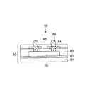
図4は本発明の第2の実施形態に係る半導体装置の断面的な構造を模式的に示したものである。
【0031】
本実施形態では、上述した第1の実施形態と同様に、半導体装置50は、パッケージとして供される配線基板60と、このパッケージ(配線基板)60内に埋設・実装された半導体チップ70とによって構成されている。
パッケージ(配線基板)60において、61は配線基板のベースとなるベース基板、62はベース基板61の上に形成された接着剤層、63は接着剤層62の上に半導体チップ70を覆うようにして形成された絶縁層としての樹脂層、64は樹脂層63の上に所要形状にパターニングされて形成された配線パターン(導体層)を示す。この配線パターン64は、樹脂層63の特定の位置において半導体チップ70の電極パッド(端子)に達するように形成されたビアホールの内部を充填するように、形成されている。また、65は配線パターン64及び樹脂層63を覆って形成された保護膜としてのソルダレジスト層、66は本装置50の外部接続端子として機能するはんだバンプを示す。ソルダレジスト層65は、配線パターン64の端子形成部分(パッド部)に対応する領域に開口部を有するように、つまり配線パターン64の端子形成部分が露出するように、形成されている。そして、この露出した配線パターン64の端子形成部分に、図示のように外部接続端子としてのはんだバンプ66が接合されている。
【0032】
また、パッケージ(配線基板)60内に埋設・実装される半導体チップ70については、第1の実施形態と同様に、厚さが50μm程度の薄いものを使用している。
本実施形態に係る半導体装置50は、厚さが50μm程度の薄い半導体チップ70をパッケージ(配線基板)60内に埋設・実装すると共に、パッケージ(配線基板)60の片面に外部接続端子としてのはんだバンプ66を設けたことを特徴としている。
【0033】
本実施形態についても、第1の実施形態と同様に、はんだバンプ(外部接続端子)66は必ずしも設ける必要はなく、要は、はんだバンプ等の外部接続端子が接続可能なように配線パターン64の一部(端子形成部分)がソルダレジスト層65から露出していれば十分である。
以下、本実施形態の半導体装置50を製造する方法について、その製造工程を示す図5を参照しながら説明する。
【0034】
先ず最初の工程では(図5(a)参照)、ベース基板61の上に接着剤を塗布し(接着剤層62)、更にこの接着剤層62の上に所要の個数の半導体チップ70(厚さが50μm程度の薄いもの)を適宜配置し、実装する。半導体チップ70の実装は、当該チップの電極パッド(端子)が形成されている側と反対側の面が接着剤層62に接着されるように行われる。
【0035】
なお、ベース基板61の材料としては、絶縁性の材料又は導電性の材料のいずれを用いてもよい。絶縁性の材料としては、例えばガラス−エポキシ樹脂、ガラスBT樹脂等が用いられ、導電性の材料としては、典型的に銅(Cu)が用いられるが、アルミニウム(Al)等の他の金属を用いてもよい。
次の工程では(図5(b)参照)、半導体チップ70を覆うようにして接着剤層62の上に絶縁層としての樹脂層63を形成する。この樹脂層63の材料としては、例えばエポキシ樹脂やポリイミド樹脂等の熱硬化性樹脂が用いられる。あるいは、感光性エポキシ樹脂や感光性ポリイミド樹脂等の感光性樹脂を用いてもよい。
【0036】
次の工程では(図5(c)参照)、樹脂層63の特定の位置において各半導体チップ70の電極パッドに達するように、CO2 レーザやエキシマレーザ等による穴明け処理によりビアホールVHを形成する(レーザビア・プロセス)。
なお、樹脂層63の材料として感光性エポキシ樹脂等の感光性樹脂を用いた場合には、ビアホールVHは、通常のフォトリソグラフィ技術を用いて形成することができる(フォトビア・プロセス)。この場合、レーザ等を用いてもビアホールVHを形成できることはもちろんである。
【0037】
この後、第1の実施形態の場合と同様に、必要に応じてデバリング、デスミア等を行う。
次の工程では(図5(d)参照)、ビアホールVH内を充填して樹脂層63の上にパターニングにより配線パターン(導体層)64を形成する。
この配線パターン(導体層)64は、例えば以下のように形成される。先ず、ビアホールVHの内部を含めて樹脂層63の上に、Cuの無電解めっきにより薄膜状Cu層を形成する。更に、この薄膜状Cu層の上に感光性のレジスト(図示せず)を塗布し、配線パターンの形状に従うように露光及び現像(レジストのパターニング)を行う。次に、このレジストパターンをめっき用のマスクとし、薄膜状Cu層をめっき給電層としてCuの電解めっきを施し、厚めの導体層を形成する。この後、レジストパターンを除去し、薄膜状Cu層の露出部分をエッチングにより除去して、図示のようにパターニングされた配線パターン(導体層)64を形成する。
【0038】
次の工程では(図5(e)参照)、配線パターン64及び樹脂層63の上に感光性のソルダレジストを塗布し、更に配線パターン64の端子形成部分の形状に従うように露光及び現像(ソルダレジストのパターニング)を行い、その端子形成部分の領域に対応する部分のソルダレジスト層に開口部を形成する。これによって、配線パターン64の端子形成部分が露出し、他の部分の配線パターン64がソルダレジスト層65によって覆われたことになる。このソルダレジスト層65は、パッケージ(配線基板)60の保護膜として機能する。
【0039】
最後の工程では(図5(f)参照)、ベース基板61と反対側の面に外部接続端子としてのはんだバンプ66を形成し、この後、個々の半導体装置50に分割する。
はんだバンプ66は、ソルダレジスト層65の開口部から露出している配線パターン64の端子形成部分にはんだボールをリフローにより接着することで、形成される。この際、第1の実施形態と同様に、はんだボールをソルダレジスト層65の開口部内に配置する前に、当該開口部の内壁にCuめっき等による導体皮膜を形成するようにすると、はんだの濡れ性を向上させる上で好適である。
【0040】
この後、ダイサー等により、破線で示すように分割線C−C’に沿って各パッケージ毎にそれぞれ1個の半導体チップ70が含まれるように分割する。これによって、図4に示す本実施形態の半導体装置50が作製されたことになる。
本実施形態についても、第1の実施形態と同様に、厚さが50μm程度の薄い半導体チップ70をパッケージ(配線基板)60内に埋設・実装しているので、半導体装置50をコンパクトに構成することができる。また、配線基板60を作製するプロセスの途中に半導体チップ70の実装工程を組み込んでいるので、従来のプロセスと比べて製造工程を簡略化することができる。
【0041】
また、図5(b)〜図5(d)の工程と同様の工程を適宜繰り返すことで、多層配線構造を容易に実現することができ、半導体装置の高機能化を図ることが可能となる。この場合、半導体チップの3次元的な配置構成及び相互間の接続は、第1の実施形態のように各パッケージ間で外部接続端子を介在して行われるのではなく、単一のパッケージ(配線基板)内で行われることになる。
【0042】
上述した各実施形態では、図3(c),図5(f)の工程において個々の半導体装置10,50に分割する前に外部接続端子(はんだバンプ32,66)を設けているが、前述したように、外部接続端子は必ずしも設ける必要はない。つまり、外部接続端子が接続可能なように配線パターン29,64の端子形成部分が露出していれば十分である。従って、図3(c),図5(f)の工程では、単に半導体装置10,50の分割処理のみを行うようにしてもよい。
【0043】
また、上述した各実施形態では半導体装置の形態としていわゆるチップ・サイズ・パッケージ(CSP)に類似した形態の場合を例にとって説明したが、半導体装置の形態はこれに限定されないことはもちろんである。例えば図3(c),図5(f)の工程において、上述した各実施形態では各パッケージ毎にそれぞれ1個の半導体チップ40,70が含まれるように(つまりCSPの形態で)分割しているが、かかる分割形態に代えて、各パッケージ毎にそれぞれ2個以上の半導体チップ40,70が含まれるように分割してもよい。このような分割形態とすることで、半導体装置をマルチ・チップ・モジュール(MCM)の形態とすることができ、半導体装置として更なる高機能化を図ることが可能となる。
【0044】
さらに、上述した第1の実施形態では図2(b)の工程において銅箔付き樹脂フィルム25を用いているが、このような銅箔付き樹脂フィルム25を用いる代わりに、絶縁層(樹脂フィルム26に相当)を形成した後で薄膜状Cu層(銅箔27に相当)を形成する工程を採用してもよい。この場合、薄膜状Cu層を形成する成膜方法としては、無電解めっき、スパッタリング、蒸着等を用いることができる。
【0045】
これは、第2の実施形態についても同様である。第2の実施形態では配線パターン64の形成に際し(図5(d)参照)、薄膜状Cu層(めっき給電層)を形成するための成膜方法として無電解めっきを用いているが、これに代えて、スパッタリングや蒸着等を用いてもよい。
【0046】
【発明の効果】
以上説明したように本発明によれば、パッケージに半導体素子を実装するに際しコンパクトに構成することができ、また、必要に応じて半導体素子の3次元的な配置構成及び相互間の接続を簡便に行うことができ、これによって高機能化を図ることが可能となる。
【図面の簡単な説明】
【図1】本発明の第1の実施形態に係る半導体装置の構造を示す断面図である。
【図2】図1の半導体装置の製造工程を示す断面図である。
【図3】図2の製造工程に続く製造工程を示す断面図である。
【図4】本発明の第2の実施形態に係る半導体装置の構造を示す断面図である。
【図5】図4の半導体装置の製造工程を示す断面図である。
【符号の説明】
10,50…半導体装置
20,60…配線基板(パッケージ)
21,61…ベース基板
22,63…樹脂層(絶縁層)
23,27…銅箔(導体層)
24,62…接着剤層
25…銅箔付き樹脂フィルム
26…樹脂フィルム(絶縁膜)
28…導体層
29,64…配線パターン(導体層)
30…樹脂(絶縁体)
31,65…ソルダレジスト層(保護膜)
32,66…はんだバンプ(外部接続端子)
40,70…半導体素子(チップ)
TH…スルーホール
VH…ビアホール
Claims (2)
- 第1の絶縁層の一方の面に配線パターンを含む第1の導体層が形成されてなるベース基板の前記第1の絶縁層の他方の面側に所要の個数の半導体素子を実装する第1の工程と、
前記半導体素子を覆うようにして第2の絶縁層を形成し、該第2の絶縁層上に配線パターンを含む第2の導体層を形成する第2の工程と、
前記第2の導体層の特定の位置に前記半導体素子の電極端子に達するようにビアホールを形成すると共に、前記半導体素子が埋設されている部分を避ける位置において上下方向に貫通するようにスルーホールを形成する第3の工程と、
前記ビアホール及びスルーホールの内壁面を含む表面全体に第3の導体層を形成する第4の工程と、
前記半導体素子の電極端子が、前記ビアホールの内壁面の導体層を介して前記第2の導体層に電気的に接続されると共に、前記スルーホールの内壁面の導体層を介して前記第1の導体層に電気的に接続されるように、前記第3の導体層にパターニングを施して配線パターンを形成する第5の工程と、
外部接続端子が接続されるべき前記第3の導体層の配線パターンの端子形成部分が露出するように配線パターン、前記第1及び第2の絶縁層を覆って保護膜を形成する第6の工程と、
該第6の工程により得られた構造体を、少なくとも1個の半導体素子が含まれるように各パッケージに分割する第7の工程とを含むことを特徴とする半導体装置の製造方法。 - 前記第6の工程後に、前記第3の導体層の配線パターンの端子形成部分に金属のバンプからなる外部接続端子を形成する工程を含むことを特徴とする請求項1に記載の半導体装置の製造方法。
Priority Applications (3)
| Application Number | Priority Date | Filing Date | Title |
|---|---|---|---|
| JP2000021913A JP3813402B2 (ja) | 2000-01-31 | 2000-01-31 | 半導体装置の製造方法 |
| US09/768,364 US6590291B2 (en) | 2000-01-31 | 2001-01-25 | Semiconductor device and manufacturing method therefor |
| US10/454,482 US6964887B2 (en) | 2000-01-31 | 2003-06-05 | Method for manufacturing semiconductor device |
Applications Claiming Priority (1)
| Application Number | Priority Date | Filing Date | Title |
|---|---|---|---|
| JP2000021913A JP3813402B2 (ja) | 2000-01-31 | 2000-01-31 | 半導体装置の製造方法 |
Publications (2)
| Publication Number | Publication Date |
|---|---|
| JP2001217337A JP2001217337A (ja) | 2001-08-10 |
| JP3813402B2 true JP3813402B2 (ja) | 2006-08-23 |
Family
ID=18548266
Family Applications (1)
| Application Number | Title | Priority Date | Filing Date |
|---|---|---|---|
| JP2000021913A Expired - Fee Related JP3813402B2 (ja) | 2000-01-31 | 2000-01-31 | 半導体装置の製造方法 |
Country Status (2)
| Country | Link |
|---|---|
| US (2) | US6590291B2 (ja) |
| JP (1) | JP3813402B2 (ja) |
Families Citing this family (179)
| Publication number | Priority date | Publication date | Assignee | Title |
|---|---|---|---|---|
| IL123207A0 (en) * | 1998-02-06 | 1998-09-24 | Shellcase Ltd | Integrated circuit device |
| JP4691074B2 (ja) * | 2000-08-14 | 2011-06-01 | 株式会社東芝 | 放射線検出システム |
| US20020020898A1 (en) * | 2000-08-16 | 2002-02-21 | Vu Quat T. | Microelectronic substrates with integrated devices |
| US20020070443A1 (en) * | 2000-12-08 | 2002-06-13 | Xiao-Chun Mu | Microelectronic package having an integrated heat sink and build-up layers |
| AU2002216352A1 (en) * | 2000-12-21 | 2002-07-01 | Shellcase Ltd. | Packaged integrated circuits and methods of producing thereof |
| JP3888854B2 (ja) * | 2001-02-16 | 2007-03-07 | シャープ株式会社 | 半導体集積回路の製造方法 |
| US6894399B2 (en) * | 2001-04-30 | 2005-05-17 | Intel Corporation | Microelectronic device having signal distribution functionality on an interfacial layer thereof |
| US6888240B2 (en) * | 2001-04-30 | 2005-05-03 | Intel Corporation | High performance, low cost microelectronic circuit package with interposer |
| US20020167804A1 (en) * | 2001-05-14 | 2002-11-14 | Intel Corporation | Polymeric encapsulation material with fibrous filler for use in microelectronic circuit packaging |
| US7071024B2 (en) * | 2001-05-21 | 2006-07-04 | Intel Corporation | Method for packaging a microelectronic device using on-die bond pad expansion |
| JP2002353369A (ja) * | 2001-05-28 | 2002-12-06 | Sharp Corp | 半導体パッケージおよびその製造方法 |
| US7183658B2 (en) * | 2001-09-05 | 2007-02-27 | Intel Corporation | Low cost microelectronic circuit package |
| JP4786836B2 (ja) * | 2001-09-07 | 2011-10-05 | 富士通セミコンダクター株式会社 | 配線接続部設計方法及び半導体装置 |
| US20030059976A1 (en) * | 2001-09-24 | 2003-03-27 | Nathan Richard J. | Integrated package and methods for making same |
| JP3813079B2 (ja) * | 2001-10-11 | 2006-08-23 | 沖電気工業株式会社 | チップサイズパッケージ |
| JP3870778B2 (ja) * | 2001-12-20 | 2007-01-24 | ソニー株式会社 | 素子内蔵基板の製造方法および素子内蔵基板 |
| TW503496B (en) | 2001-12-31 | 2002-09-21 | Megic Corp | Chip packaging structure and manufacturing process of the same |
| TW544882B (en) | 2001-12-31 | 2003-08-01 | Megic Corp | Chip package structure and process thereof |
| US6673698B1 (en) | 2002-01-19 | 2004-01-06 | Megic Corporation | Thin film semiconductor package utilizing a glass substrate with composite polymer/metal interconnect layers |
| TW517361B (en) | 2001-12-31 | 2003-01-11 | Megic Corp | Chip package structure and its manufacture process |
| TW584950B (en) | 2001-12-31 | 2004-04-21 | Megic Corp | Chip packaging structure and process thereof |
| JP2003289073A (ja) * | 2002-01-22 | 2003-10-10 | Canon Inc | 半導体装置および半導体装置の製造方法 |
| TW200302685A (en) * | 2002-01-23 | 2003-08-01 | Matsushita Electric Industrial Co Ltd | Circuit component built-in module and method of manufacturing the same |
| TW577160B (en) * | 2002-02-04 | 2004-02-21 | Casio Computer Co Ltd | Semiconductor device and manufacturing method thereof |
| US20030153119A1 (en) * | 2002-02-14 | 2003-08-14 | Nathan Richard J. | Integrated circuit package and method for fabrication |
| US9691635B1 (en) * | 2002-05-01 | 2017-06-27 | Amkor Technology, Inc. | Buildup dielectric layer having metallization pattern semiconductor package fabrication method |
| DE10224124A1 (de) * | 2002-05-29 | 2003-12-18 | Infineon Technologies Ag | Elektronisches Bauteil mit äußeren Flächenkontakten und Verfahren zu seiner Herstellung |
| US7485489B2 (en) * | 2002-06-19 | 2009-02-03 | Bjoersell Sten | Electronics circuit manufacture |
| JP4363823B2 (ja) * | 2002-07-04 | 2009-11-11 | 富士通マイクロエレクトロニクス株式会社 | 半導体装置の実装システム |
| JP3657246B2 (ja) * | 2002-07-29 | 2005-06-08 | Necエレクトロニクス株式会社 | 半導体装置 |
| WO2004015771A2 (en) * | 2002-08-09 | 2004-02-19 | Casio Computer Co., Ltd. | Semiconductor device and method of manufacturing the same |
| DE10239081B4 (de) | 2002-08-26 | 2007-12-20 | Qimonda Ag | Verfahren zur Herstellung einer Halbleitereinrichtung |
| US6790758B2 (en) * | 2002-11-25 | 2004-09-14 | Silicon Integrated Systems Corp. | Method for fabricating conductive bumps and substrate with metal bumps for flip chip packaging |
| JP4209178B2 (ja) * | 2002-11-26 | 2009-01-14 | 新光電気工業株式会社 | 電子部品実装構造及びその製造方法 |
| US20040124546A1 (en) * | 2002-12-29 | 2004-07-01 | Mukul Saran | Reliable integrated circuit and package |
| KR100499006B1 (ko) * | 2002-12-30 | 2005-07-01 | 삼성전기주식회사 | 도금 인입선이 없는 패키지 기판의 제조 방법 |
| JP3740469B2 (ja) * | 2003-01-31 | 2006-02-01 | 株式会社東芝 | 半導体装置および半導体装置の製造方法 |
| SG137651A1 (en) * | 2003-03-14 | 2007-12-28 | Micron Technology Inc | Microelectronic devices and methods for packaging microelectronic devices |
| JP4289146B2 (ja) * | 2003-03-27 | 2009-07-01 | セイコーエプソン株式会社 | 三次元実装型半導体装置の製造方法 |
| US7141874B2 (en) * | 2003-05-14 | 2006-11-28 | Matsushita Electric Industrial Co., Ltd. | Electronic component packaging structure and method for producing the same |
| EP1636842B1 (en) | 2003-06-03 | 2011-08-17 | Casio Computer Co., Ltd. | Stackable semiconductor device and method of manufacturing the same |
| KR100604821B1 (ko) * | 2003-06-30 | 2006-07-26 | 삼성전자주식회사 | 적층형 볼 그리드 어레이 패키지 및 그 제조방법 |
| FI20031341L (fi) | 2003-09-18 | 2005-03-19 | Imbera Electronics Oy | Menetelmä elektroniikkamoduulin valmistamiseksi |
| TWI278048B (en) | 2003-11-10 | 2007-04-01 | Casio Computer Co Ltd | Semiconductor device and its manufacturing method |
| JP4321758B2 (ja) * | 2003-11-26 | 2009-08-26 | カシオ計算機株式会社 | 半導体装置 |
| JP4379693B2 (ja) * | 2003-11-10 | 2009-12-09 | カシオ計算機株式会社 | 半導体装置およびその製造方法 |
| JP4324732B2 (ja) * | 2003-11-28 | 2009-09-02 | カシオ計算機株式会社 | 半導体装置の製造方法 |
| CN100418211C (zh) * | 2003-12-25 | 2008-09-10 | 卡西欧计算机株式会社 | 半导体器件及其制造方法 |
| US7489032B2 (en) * | 2003-12-25 | 2009-02-10 | Casio Computer Co., Ltd. | Semiconductor device including a hard sheet to reduce warping of a base plate and method of fabricating the same |
| JP4271590B2 (ja) | 2004-01-20 | 2009-06-03 | 新光電気工業株式会社 | 半導体装置及びその製造方法 |
| JP3945483B2 (ja) | 2004-01-27 | 2007-07-18 | カシオ計算機株式会社 | 半導体装置の製造方法 |
| JP4093186B2 (ja) * | 2004-01-27 | 2008-06-04 | カシオ計算機株式会社 | 半導体装置の製造方法 |
| JP4204989B2 (ja) | 2004-01-30 | 2009-01-07 | 新光電気工業株式会社 | 半導体装置及びその製造方法 |
| JP4298559B2 (ja) | 2004-03-29 | 2009-07-22 | 新光電気工業株式会社 | 電子部品実装構造及びその製造方法 |
| JP3925809B2 (ja) | 2004-03-31 | 2007-06-06 | カシオ計算機株式会社 | 半導体装置およびその製造方法 |
| JP4528018B2 (ja) * | 2004-04-26 | 2010-08-18 | 新光電気工業株式会社 | 半導体装置及びその製造方法 |
| JP4541753B2 (ja) * | 2004-05-10 | 2010-09-08 | 新光電気工業株式会社 | 電子部品実装構造の製造方法 |
| CN1312763C (zh) * | 2004-05-14 | 2007-04-25 | 相互股份有限公司 | 芯片埋入式半导体元件封装结构 |
| JP2005327984A (ja) * | 2004-05-17 | 2005-11-24 | Shinko Electric Ind Co Ltd | 電子部品及び電子部品実装構造の製造方法 |
| US7179738B2 (en) * | 2004-06-17 | 2007-02-20 | Texas Instruments Incorporated | Semiconductor assembly having substrate with electroplated contact pads |
| JP2006013205A (ja) * | 2004-06-28 | 2006-01-12 | Akita Denshi Systems:Kk | 半導体装置及びその製造方法 |
| JP2006019340A (ja) * | 2004-06-30 | 2006-01-19 | Tdk Corp | 半導体ic内蔵基板 |
| KR100575591B1 (ko) * | 2004-07-27 | 2006-05-03 | 삼성전자주식회사 | 웨이퍼 레벨 적층 패키지용 칩 스케일 패키지 및 그 제조 방법 |
| JP2006041512A (ja) * | 2004-07-27 | 2006-02-09 | Samsung Electronics Co Ltd | マルチチップパッケージ用集積回路チップの製造方法及びその方法により形成されたウエハ及びチップ |
| JP2006041438A (ja) * | 2004-07-30 | 2006-02-09 | Shinko Electric Ind Co Ltd | 半導体チップ内蔵基板及びその製造方法 |
| JP4575071B2 (ja) * | 2004-08-02 | 2010-11-04 | 新光電気工業株式会社 | 電子部品内蔵基板の製造方法 |
| US20060278976A1 (en) * | 2004-09-02 | 2006-12-14 | Koninklijke Phillips Electronics N.C. | Semiconductor device, method and manufacturing same, identification label and information carrier |
| TWI241007B (en) * | 2004-09-09 | 2005-10-01 | Phoenix Prec Technology Corp | Semiconductor device embedded structure and method for fabricating the same |
| JP2006100666A (ja) * | 2004-09-30 | 2006-04-13 | Toshiba Corp | 半導体装置及びその製造方法 |
| US7049208B2 (en) * | 2004-10-11 | 2006-05-23 | Intel Corporation | Method of manufacturing of thin based substrate |
| US7411303B2 (en) * | 2004-11-09 | 2008-08-12 | Texas Instruments Incorporated | Semiconductor assembly having substrate with electroplated contact pads |
| TWI241695B (en) * | 2004-11-19 | 2005-10-11 | Ind Tech Res Inst | Structure of an electronic package and method for fabricating the same |
| JP4880218B2 (ja) * | 2004-12-22 | 2012-02-22 | 三洋電機株式会社 | 回路装置 |
| JP2006269594A (ja) * | 2005-03-23 | 2006-10-05 | Cmk Corp | 半導体装置及びその製造方法 |
| TWI283553B (en) * | 2005-04-21 | 2007-07-01 | Ind Tech Res Inst | Thermal enhanced low profile package structure and method for fabricating the same |
| JP2006332094A (ja) | 2005-05-23 | 2006-12-07 | Seiko Epson Corp | 電子基板の製造方法及び半導体装置の製造方法並びに電子機器の製造方法 |
| JP2006351565A (ja) * | 2005-06-13 | 2006-12-28 | Shinko Electric Ind Co Ltd | 積層型半導体パッケージ |
| JP5134194B2 (ja) * | 2005-07-19 | 2013-01-30 | ナミックス株式会社 | 部品内蔵デバイス及び製造方法 |
| US7566853B2 (en) * | 2005-08-12 | 2009-07-28 | Tessera, Inc. | Image sensor employing a plurality of photodetector arrays and/or rear-illuminated architecture |
| JP4535002B2 (ja) * | 2005-09-28 | 2010-09-01 | Tdk株式会社 | 半導体ic内蔵基板及びその製造方法 |
| JP2007103716A (ja) * | 2005-10-05 | 2007-04-19 | Sony Corp | 半導体装置及びその製造方法 |
| JP2007103715A (ja) * | 2005-10-05 | 2007-04-19 | Sony Corp | 半導体装置及びその製造方法 |
| JP4593444B2 (ja) * | 2005-11-07 | 2010-12-08 | 新光電気工業株式会社 | 電子部品実装構造体の製造方法 |
| JP4826248B2 (ja) * | 2005-12-19 | 2011-11-30 | Tdk株式会社 | Ic内蔵基板の製造方法 |
| TWI284402B (en) * | 2005-12-30 | 2007-07-21 | Advanced Semiconductor Eng | Build-up package and method of an optoelectronic chip |
| TWI310968B (en) * | 2006-02-09 | 2009-06-11 | Phoenix Prec Technology Corp | Electrically connecting structure of circuit board with semiconductor chip embedded therein |
| KR100736635B1 (ko) | 2006-02-09 | 2007-07-06 | 삼성전기주식회사 | 베어칩 내장형 인쇄회로기판 및 그 제조 방법 |
| TWI412079B (zh) * | 2006-07-28 | 2013-10-11 | 半導體能源研究所股份有限公司 | 製造顯示裝置的方法 |
| US7943287B2 (en) * | 2006-07-28 | 2011-05-17 | Semiconductor Energy Laboratory Co., Ltd. | Method for manufacturing display device |
| JP2008047753A (ja) * | 2006-08-18 | 2008-02-28 | Cmk Corp | 半導体装置及びその製造方法 |
| KR101346246B1 (ko) * | 2006-08-24 | 2013-12-31 | 가부시키가이샤 한도오따이 에네루기 켄큐쇼 | 표시장치 제작방법 |
| US8563431B2 (en) * | 2006-08-25 | 2013-10-22 | Semiconductor Energy Laboratory Co., Ltd. | Method for manufacturing semiconductor device |
| US8148259B2 (en) | 2006-08-30 | 2012-04-03 | Semiconductor Energy Laboratory Co., Ltd. | Method for manufacturing semiconductor device |
| US7807508B2 (en) * | 2006-10-31 | 2010-10-05 | Tessera Technologies Hungary Kft. | Wafer-level fabrication of lidded chips with electrodeposited dielectric coating |
| US7480364B2 (en) * | 2006-11-03 | 2009-01-20 | General Electric Company | High voltage tank assembly for radiation generator |
| KR100817073B1 (ko) * | 2006-11-03 | 2008-03-26 | 삼성전자주식회사 | 휨방지용 보강부재가 기판에 연결된 반도체 칩 스택 패키지 |
| JP4480710B2 (ja) * | 2006-12-04 | 2010-06-16 | Okiセミコンダクタ株式会社 | 半導体装置内蔵基板 |
| KR100833194B1 (ko) * | 2006-12-19 | 2008-05-28 | 삼성전자주식회사 | 반도체 칩의 배선층이 기판에 직접 연결된 반도체 패키지및 그 제조방법 |
| JP2008159820A (ja) * | 2006-12-22 | 2008-07-10 | Tdk Corp | 電子部品の一括実装方法、及び電子部品内蔵基板の製造方法 |
| US7579215B2 (en) * | 2007-03-30 | 2009-08-25 | Motorola, Inc. | Method for fabricating a low cost integrated circuit (IC) package |
| US8829663B2 (en) * | 2007-07-02 | 2014-09-09 | Infineon Technologies Ag | Stackable semiconductor package with encapsulant and electrically conductive feed-through |
| JP4752825B2 (ja) * | 2007-08-24 | 2011-08-17 | カシオ計算機株式会社 | 半導体装置の製造方法 |
| KR100881400B1 (ko) * | 2007-09-10 | 2009-02-02 | 주식회사 하이닉스반도체 | 반도체 패키지 및 이의 제조 방법 |
| KR100869832B1 (ko) * | 2007-09-18 | 2008-11-21 | 삼성전기주식회사 | 반도체칩 패키지 및 이를 이용한 인쇄회로기판 |
| TWI360207B (en) | 2007-10-22 | 2012-03-11 | Advanced Semiconductor Eng | Chip package structure and method of manufacturing |
| US8390117B2 (en) * | 2007-12-11 | 2013-03-05 | Panasonic Corporation | Semiconductor device and method of manufacturing the same |
| JP4840373B2 (ja) * | 2008-01-31 | 2011-12-21 | カシオ計算機株式会社 | 半導体装置およびその製造方法 |
| JP4636090B2 (ja) | 2008-01-31 | 2011-02-23 | カシオ計算機株式会社 | 半導体装置およびその製造方法 |
| TW200935572A (en) * | 2008-02-01 | 2009-08-16 | Yu-Nung Shen | Semiconductor chip packaging body and its packaging method |
| US8507320B2 (en) * | 2008-03-18 | 2013-08-13 | Infineon Technologies Ag | Electronic device including a carrier and a semiconductor chip attached to the carrier and manufacturing thereof |
| FI123205B (fi) | 2008-05-12 | 2012-12-31 | Imbera Electronics Oy | Piirimoduuli ja menetelmä piirimoduulin valmistamiseksi |
| TWI387074B (zh) * | 2008-06-05 | 2013-02-21 | 南茂科技股份有限公司 | 晶粒堆疊結構及其形成方法 |
| TWI387014B (zh) * | 2008-06-05 | 2013-02-21 | 南茂科技股份有限公司 | 具有犧牲基板之晶粒重新配置結構及其封裝方法 |
| JP5289830B2 (ja) | 2008-06-06 | 2013-09-11 | ルネサスエレクトロニクス株式会社 | 半導体装置 |
| TWI453877B (zh) * | 2008-11-07 | 2014-09-21 | 日月光半導體製造股份有限公司 | 內埋晶片封裝的結構及製程 |
| JP4787296B2 (ja) * | 2008-07-18 | 2011-10-05 | Tdk株式会社 | 半導体内蔵モジュール及びその製造方法 |
| FI122217B (fi) | 2008-07-22 | 2011-10-14 | Imbera Electronics Oy | Monisirupaketti ja valmistusmenetelmä |
| KR101013555B1 (ko) * | 2008-10-09 | 2011-02-14 | 주식회사 하이닉스반도체 | 반도체 패키지 및 이의 제조 방법 |
| JP5436836B2 (ja) * | 2008-10-30 | 2014-03-05 | 新光電気工業株式会社 | 半導体装置内蔵基板の製造方法 |
| TWI501359B (zh) * | 2009-03-13 | 2015-09-21 | 精材科技股份有限公司 | 電子元件封裝體及其形成方法 |
| KR20100109241A (ko) * | 2009-03-31 | 2010-10-08 | 삼성전자주식회사 | 칩 적층 패키지 및 그 제조방법 |
| WO2010129002A1 (en) * | 2009-05-04 | 2010-11-11 | R&D Circuits Inc. | Method and apparatus for improving power and loss for interconect configurations |
| US8836036B2 (en) * | 2010-01-05 | 2014-09-16 | Globalfoundries Singapore Pte. Ltd. | Method for fabricating semiconductor devices using stress engineering |
| US8569894B2 (en) | 2010-01-13 | 2013-10-29 | Advanced Semiconductor Engineering, Inc. | Semiconductor package with single sided substrate design and manufacturing methods thereof |
| US8320134B2 (en) | 2010-02-05 | 2012-11-27 | Advanced Semiconductor Engineering, Inc. | Embedded component substrate and manufacturing methods thereof |
| US8513062B2 (en) * | 2010-02-16 | 2013-08-20 | Infineon Technologies Ag | Method of manufacturing a semiconductor device with a carrier having a cavity and semiconductor device |
| JP5232185B2 (ja) * | 2010-03-05 | 2013-07-10 | 株式会社東芝 | 半導体装置の製造方法 |
| TWI411075B (zh) | 2010-03-22 | 2013-10-01 | 日月光半導體製造股份有限公司 | 半導體封裝件及其製造方法 |
| US8183696B2 (en) | 2010-03-31 | 2012-05-22 | Infineon Technologies Ag | Packaged semiconductor device with encapsulant embedding semiconductor chip that includes contact pads |
| TWI400783B (zh) * | 2010-07-21 | 2013-07-01 | 日月光半導體製造股份有限公司 | 封裝結構及其製作方法 |
| KR20120026855A (ko) * | 2010-09-10 | 2012-03-20 | 삼성전기주식회사 | 임베디드 볼 그리드 어레이 기판 및 그 제조 방법 |
| DE102010041129A1 (de) * | 2010-09-21 | 2012-03-22 | Robert Bosch Gmbh | Multifunktionssensor als PoP-mWLP |
| US8546922B2 (en) * | 2010-09-30 | 2013-10-01 | Ibiden Co., Ltd. | Wiring board |
| US9406658B2 (en) | 2010-12-17 | 2016-08-02 | Advanced Semiconductor Engineering, Inc. | Embedded component device and manufacturing methods thereof |
| US8623702B2 (en) * | 2011-02-24 | 2014-01-07 | Stats Chippac, Ltd. | Semiconductor device and method of forming conductive THV and RDL on opposite sides of semiconductor die for RDL-to-RDL bonding |
| US8487426B2 (en) | 2011-03-15 | 2013-07-16 | Advanced Semiconductor Engineering, Inc. | Semiconductor package with embedded die and manufacturing methods thereof |
| US8461691B2 (en) * | 2011-04-29 | 2013-06-11 | Infineon Technologies Ag | Chip-packaging module for a chip and a method for forming a chip-packaging module |
| JP2013030593A (ja) * | 2011-07-28 | 2013-02-07 | J Devices:Kk | 半導体装置、該半導体装置を垂直に積層した半導体モジュール構造及びその製造方法 |
| US8552556B1 (en) | 2011-11-22 | 2013-10-08 | Amkor Technology, Inc. | Wafer level fan out package |
| JP2013115136A (ja) * | 2011-11-25 | 2013-06-10 | Ibiden Co Ltd | 電子部品内蔵基板及びその製造方法 |
| US9171823B2 (en) | 2011-12-30 | 2015-10-27 | Stmicroelectronics Pte Ltd | Circuit module with multiple submodules |
| TWI509712B (zh) * | 2012-01-20 | 2015-11-21 | 東琳精密股份有限公司 | 晶片尺寸封裝結構及其晶片尺寸封裝方法 |
| JP5977051B2 (ja) * | 2012-03-21 | 2016-08-24 | 新光電気工業株式会社 | 半導体パッケージ、半導体装置及び半導体パッケージの製造方法 |
| TWI463619B (zh) * | 2012-06-22 | 2014-12-01 | 矽品精密工業股份有限公司 | 半導體封裝件及其製法 |
| JP6034664B2 (ja) * | 2012-11-05 | 2016-11-30 | 株式会社ジェイデバイス | 半導体装置、半導体積層モジュール構造、積層モジュール構造、及びこれらの製造方法 |
| KR101472640B1 (ko) * | 2012-12-31 | 2014-12-15 | 삼성전기주식회사 | 회로 기판 및 회로 기판 제조방법 |
| JP6144058B2 (ja) | 2013-01-31 | 2017-06-07 | 新光電気工業株式会社 | 配線基板及び配線基板の製造方法 |
| US8941244B1 (en) * | 2013-07-03 | 2015-01-27 | Taiwan Semiconductor Manufacturing Company Ltd. | Semiconductor device and manufacturing method thereof |
| US9318411B2 (en) | 2013-11-13 | 2016-04-19 | Brodge Semiconductor Corporation | Semiconductor package with package-on-package stacking capability and method of manufacturing the same |
| US9209154B2 (en) | 2013-12-04 | 2015-12-08 | Bridge Semiconductor Corporation | Semiconductor package with package-on-package stacking capability and method of manufacturing the same |
| CN104952858B (zh) * | 2014-03-24 | 2019-03-08 | 株式会社吉帝伟士 | 半导体器件、半导体层叠模块构造、层叠模块构造以及它们的制造方法 |
| JP6332672B2 (ja) | 2014-04-16 | 2018-05-30 | 新光電気工業株式会社 | 電池内蔵基板及びその製造方法 |
| US20150379302A1 (en) * | 2014-06-25 | 2015-12-31 | Ned Smith | Privacy enhanced email service |
| US9502270B2 (en) | 2014-07-08 | 2016-11-22 | Taiwan Semiconductor Manufacturing Company, Ltd. | Semiconductor device packages, packaging methods, and packaged semiconductor devices |
| JP6418686B2 (ja) * | 2014-12-25 | 2018-11-07 | 株式会社ジェイデバイス | 半導体装置及びその製造方法 |
| US10679965B2 (en) * | 2015-02-04 | 2020-06-09 | Zowie Technology Corporation | Semiconductor package structure with preferred heat dissipating efficacy without formation of short circuit |
| TWI569368B (zh) | 2015-03-06 | 2017-02-01 | 恆勁科技股份有限公司 | 封裝基板、包含該封裝基板的封裝結構及其製作方法 |
| JP6269626B2 (ja) * | 2015-09-11 | 2018-01-31 | Tdk株式会社 | 半導体装置、電子部品内蔵基板、及びこれらの製造方法 |
| JP6862087B2 (ja) | 2015-12-11 | 2021-04-21 | 株式会社アムコー・テクノロジー・ジャパン | 配線基板、配線基板を有する半導体パッケージ、およびその製造方法 |
| US10068855B2 (en) * | 2016-09-12 | 2018-09-04 | Samsung Electro-Mechanics Co., Ltd. | Semiconductor package, method of manufacturing the same, and electronic device module |
| CN106358374A (zh) * | 2016-10-26 | 2017-01-25 | 广东骏亚电子科技股份有限公司 | 一种改善异型槽孔孔内毛刺的方法 |
| EP3553816A4 (en) * | 2016-12-08 | 2020-05-06 | Hitachi Chemical Co., Ltd. | METHOD FOR PRODUCING A SEMICONDUCTOR COMPONENT |
| US10269671B2 (en) * | 2017-01-03 | 2019-04-23 | Powertech Technology Inc. | Package structure and manufacturing method thereof |
| US10211137B2 (en) * | 2017-06-08 | 2019-02-19 | Advanced Semiconductor Engineering, Inc. | Semiconductor device package |
| US10304765B2 (en) * | 2017-06-08 | 2019-05-28 | Advanced Semiconductor Engineering, Inc. | Semiconductor device package |
| US11477884B2 (en) * | 2018-04-04 | 2022-10-18 | Sumitomo Electric Printed Circuits, Inc. | Cover film for flexible printed circuit board and flexible printed circuit board |
| CN108831875B (zh) * | 2018-08-10 | 2024-03-05 | 浙江熔城半导体有限公司 | 滤波器芯片内嵌且电极外设的封装结构及其制作方法 |
| US20200312732A1 (en) | 2018-09-14 | 2020-10-01 | Mediatek Inc. | Chip scale package structure and method of forming the same |
| US11450606B2 (en) | 2018-09-14 | 2022-09-20 | Mediatek Inc. | Chip scale package structure and method of forming the same |
| TWI718011B (zh) * | 2019-02-26 | 2021-02-01 | 日商長瀨產業股份有限公司 | 嵌入式半導體封裝及其方法 |
| JP7371882B2 (ja) * | 2019-04-12 | 2023-10-31 | 株式会社ライジングテクノロジーズ | 電子回路装置および電子回路装置の製造方法 |
| WO2020250795A1 (ja) | 2019-06-10 | 2020-12-17 | 株式会社ライジングテクノロジーズ | 電子回路装置 |
| CN112770495B (zh) * | 2019-10-21 | 2022-05-27 | 宏启胜精密电子(秦皇岛)有限公司 | 全向内埋模组及制作方法、封装结构及制作方法 |
| US12538820B2 (en) * | 2020-10-29 | 2026-01-27 | Mitsubishi Electric Corporation | Semiconductor package, semiconductor device, and power conversion device |
| JP7516230B2 (ja) * | 2020-12-03 | 2024-07-16 | 新光電気工業株式会社 | 半導体装置及び半導体装置の製造方法 |
| EP4030476A1 (en) * | 2021-01-15 | 2022-07-20 | Mitsubishi Electric R & D Centre Europe B.V. | An integrated cooling liquid cavity in a printed circuit board and a method to make the same |
| US11990399B2 (en) * | 2021-09-24 | 2024-05-21 | Texas Instruments Incorporated | Device with dummy metallic traces |
| CN114666995B (zh) * | 2022-02-25 | 2024-03-26 | 珠海越亚半导体股份有限公司 | 封装基板及其制作方法 |
| TWI871519B (zh) * | 2022-06-17 | 2025-02-01 | 華東科技股份有限公司 | 多層堆疊式晶片封裝及其製造方法 |
Family Cites Families (15)
| Publication number | Priority date | Publication date | Assignee | Title |
|---|---|---|---|---|
| JP3094481B2 (ja) * | 1991-03-13 | 2000-10-03 | 松下電器産業株式会社 | 電子回路装置とその製造方法 |
| US5111278A (en) * | 1991-03-27 | 1992-05-05 | Eichelberger Charles W | Three-dimensional multichip module systems |
| US6355976B1 (en) * | 1992-05-14 | 2002-03-12 | Reveo, Inc | Three-dimensional packaging technology for multi-layered integrated circuits |
| US5783870A (en) * | 1995-03-16 | 1998-07-21 | National Semiconductor Corporation | Method for connecting packages of a stacked ball grid array structure |
| JP3015712B2 (ja) * | 1995-06-30 | 2000-03-06 | 日東電工株式会社 | フィルムキャリアおよびそれを用いてなる半導体装置 |
| US5567657A (en) * | 1995-12-04 | 1996-10-22 | General Electric Company | Fabrication and structures of two-sided molded circuit modules with flexible interconnect layers |
| KR100234719B1 (ko) * | 1997-03-14 | 1999-12-15 | 김영환 | 에리어 어레이 패키지 및 그 제조방법 |
| CN1106036C (zh) * | 1997-05-15 | 2003-04-16 | 日本电气株式会社 | 芯片型半导体装置的制造方法 |
| JPH11111738A (ja) * | 1997-10-07 | 1999-04-23 | Oki Electric Ind Co Ltd | Cob及びcobの製造方法,半導体素子及び半導体素子の製造方法 |
| JPH11168150A (ja) * | 1997-12-04 | 1999-06-22 | Mitsubishi Electric Corp | 半導体集積回路装置 |
| KR100266693B1 (ko) * | 1998-05-30 | 2000-09-15 | 김영환 | 적층가능한 비지에이 반도체 칩 패키지 및 그 제조방법 |
| JPH11354667A (ja) * | 1998-06-05 | 1999-12-24 | Nippon Telegr & Teleph Corp <Ntt> | 電子部品およびその実装方法 |
| JP2000022040A (ja) * | 1998-07-07 | 2000-01-21 | Mitsubishi Electric Corp | 半導体装置およびその製造方法 |
| US6075712A (en) * | 1999-01-08 | 2000-06-13 | Intel Corporation | Flip-chip having electrical contact pads on the backside of the chip |
| US6271469B1 (en) * | 1999-11-12 | 2001-08-07 | Intel Corporation | Direct build-up layer on an encapsulated die package |
-
2000
- 2000-01-31 JP JP2000021913A patent/JP3813402B2/ja not_active Expired - Fee Related
-
2001
- 2001-01-25 US US09/768,364 patent/US6590291B2/en not_active Expired - Lifetime
-
2003
- 2003-06-05 US US10/454,482 patent/US6964887B2/en not_active Expired - Lifetime
Also Published As
| Publication number | Publication date |
|---|---|
| US20030209806A1 (en) | 2003-11-13 |
| US6964887B2 (en) | 2005-11-15 |
| US20010010627A1 (en) | 2001-08-02 |
| US6590291B2 (en) | 2003-07-08 |
| JP2001217337A (ja) | 2001-08-10 |
Similar Documents
| Publication | Publication Date | Title |
|---|---|---|
| JP3813402B2 (ja) | 半導体装置の製造方法 | |
| JP4251421B2 (ja) | 半導体装置の製造方法 | |
| US7791206B2 (en) | Semiconductor device and method of manufacturing the same | |
| US7723838B2 (en) | Package structure having semiconductor device embedded within wiring board | |
| US7122901B2 (en) | Semiconductor device | |
| US7501696B2 (en) | Semiconductor chip-embedded substrate and method of manufacturing same | |
| US8209856B2 (en) | Printed wiring board and method for manufacturing the same | |
| US8222747B2 (en) | Multilayer wiring substrate mounted with electronic component and method for manufacturing the same | |
| JP4790297B2 (ja) | 半導体装置およびその製造方法 | |
| JP5221315B2 (ja) | 配線基板及びその製造方法 | |
| CN101276809A (zh) | 半导体器件及其制造方法 | |
| JP5406572B2 (ja) | 電子部品内蔵配線基板及びその製造方法 | |
| JP2005294451A (ja) | 半導体集積回路の製造方法および半導体集積回路ならびに半導体集積回路装置 | |
| US20040256715A1 (en) | Wiring board, semiconductor device and process of fabricating wiring board | |
| JP2010123632A (ja) | 電子部品内蔵配線基板の製造方法 | |
| JP4528018B2 (ja) | 半導体装置及びその製造方法 | |
| JP2025057775A (ja) | 配線基板及びその製造方法、半導体装置 |
Legal Events
| Date | Code | Title | Description |
|---|---|---|---|
| A977 | Report on retrieval |
Free format text: JAPANESE INTERMEDIATE CODE: A971007 Effective date: 20040805 |
|
| A131 | Notification of reasons for refusal |
Free format text: JAPANESE INTERMEDIATE CODE: A131 Effective date: 20050719 |
|
| A521 | Request for written amendment filed |
Free format text: JAPANESE INTERMEDIATE CODE: A523 Effective date: 20050920 |
|
| TRDD | Decision of grant or rejection written | ||
| A01 | Written decision to grant a patent or to grant a registration (utility model) |
Free format text: JAPANESE INTERMEDIATE CODE: A01 Effective date: 20060530 |
|
| A61 | First payment of annual fees (during grant procedure) |
Free format text: JAPANESE INTERMEDIATE CODE: A61 Effective date: 20060531 |
|
| R150 | Certificate of patent or registration of utility model |
Ref document number: 3813402 Country of ref document: JP Free format text: JAPANESE INTERMEDIATE CODE: R150 Free format text: JAPANESE INTERMEDIATE CODE: R150 |
|
| FPAY | Renewal fee payment (event date is renewal date of database) |
Free format text: PAYMENT UNTIL: 20090609 Year of fee payment: 3 |
|
| FPAY | Renewal fee payment (event date is renewal date of database) |
Free format text: PAYMENT UNTIL: 20100609 Year of fee payment: 4 |
|
| FPAY | Renewal fee payment (event date is renewal date of database) |
Free format text: PAYMENT UNTIL: 20110609 Year of fee payment: 5 |
|
| FPAY | Renewal fee payment (event date is renewal date of database) |
Free format text: PAYMENT UNTIL: 20110609 Year of fee payment: 5 |
|
| FPAY | Renewal fee payment (event date is renewal date of database) |
Free format text: PAYMENT UNTIL: 20120609 Year of fee payment: 6 |
|
| FPAY | Renewal fee payment (event date is renewal date of database) |
Free format text: PAYMENT UNTIL: 20120609 Year of fee payment: 6 |
|
| FPAY | Renewal fee payment (event date is renewal date of database) |
Free format text: PAYMENT UNTIL: 20130609 Year of fee payment: 7 |
|
| LAPS | Cancellation because of no payment of annual fees |