JP4324732B2 - 半導体装置の製造方法 - Google Patents
半導体装置の製造方法 Download PDFInfo
- Publication number
- JP4324732B2 JP4324732B2 JP2003398540A JP2003398540A JP4324732B2 JP 4324732 B2 JP4324732 B2 JP 4324732B2 JP 2003398540 A JP2003398540 A JP 2003398540A JP 2003398540 A JP2003398540 A JP 2003398540A JP 4324732 B2 JP4324732 B2 JP 4324732B2
- Authority
- JP
- Japan
- Prior art keywords
- wiring
- wiring board
- semiconductor
- opening
- semiconductor structure
- Prior art date
- Legal status (The legal status is an assumption and is not a legal conclusion. Google has not performed a legal analysis and makes no representation as to the accuracy of the status listed.)
- Expired - Fee Related
Links
Images


Classifications
-
- H—ELECTRICITY
- H01—ELECTRIC ELEMENTS
- H01L—SEMICONDUCTOR DEVICES NOT COVERED BY CLASS H10
- H01L24/00—Arrangements for connecting or disconnecting semiconductor or solid-state bodies; Methods or apparatus related thereto
- H01L24/01—Means for bonding being attached to, or being formed on, the surface to be connected, e.g. chip-to-package, die-attach, "first-level" interconnects; Manufacturing methods related thereto
- H01L24/18—High density interconnect [HDI] connectors; Manufacturing methods related thereto
- H01L24/19—Manufacturing methods of high density interconnect preforms
-
- H—ELECTRICITY
- H01—ELECTRIC ELEMENTS
- H01L—SEMICONDUCTOR DEVICES NOT COVERED BY CLASS H10
- H01L2224/00—Indexing scheme for arrangements for connecting or disconnecting semiconductor or solid-state bodies and methods related thereto as covered by H01L24/00
- H01L2224/01—Means for bonding being attached to, or being formed on, the surface to be connected, e.g. chip-to-package, die-attach, "first-level" interconnects; Manufacturing methods related thereto
- H01L2224/10—Bump connectors; Manufacturing methods related thereto
- H01L2224/12—Structure, shape, material or disposition of the bump connectors prior to the connecting process
- H01L2224/12105—Bump connectors formed on an encapsulation of the semiconductor or solid-state body, e.g. bumps on chip-scale packages
-
- H—ELECTRICITY
- H01—ELECTRIC ELEMENTS
- H01L—SEMICONDUCTOR DEVICES NOT COVERED BY CLASS H10
- H01L2224/00—Indexing scheme for arrangements for connecting or disconnecting semiconductor or solid-state bodies and methods related thereto as covered by H01L24/00
- H01L2224/01—Means for bonding being attached to, or being formed on, the surface to be connected, e.g. chip-to-package, die-attach, "first-level" interconnects; Manufacturing methods related thereto
- H01L2224/10—Bump connectors; Manufacturing methods related thereto
- H01L2224/15—Structure, shape, material or disposition of the bump connectors after the connecting process
- H01L2224/16—Structure, shape, material or disposition of the bump connectors after the connecting process of an individual bump connector
- H01L2224/161—Disposition
- H01L2224/16151—Disposition the bump connector connecting between a semiconductor or solid-state body and an item not being a semiconductor or solid-state body, e.g. chip-to-substrate, chip-to-passive
- H01L2224/16221—Disposition the bump connector connecting between a semiconductor or solid-state body and an item not being a semiconductor or solid-state body, e.g. chip-to-substrate, chip-to-passive the body and the item being stacked
- H01L2224/16225—Disposition the bump connector connecting between a semiconductor or solid-state body and an item not being a semiconductor or solid-state body, e.g. chip-to-substrate, chip-to-passive the body and the item being stacked the item being non-metallic, e.g. insulating substrate with or without metallisation
-
- H—ELECTRICITY
- H01—ELECTRIC ELEMENTS
- H01L—SEMICONDUCTOR DEVICES NOT COVERED BY CLASS H10
- H01L2224/00—Indexing scheme for arrangements for connecting or disconnecting semiconductor or solid-state bodies and methods related thereto as covered by H01L24/00
- H01L2224/01—Means for bonding being attached to, or being formed on, the surface to be connected, e.g. chip-to-package, die-attach, "first-level" interconnects; Manufacturing methods related thereto
- H01L2224/18—High density interconnect [HDI] connectors; Manufacturing methods related thereto
- H01L2224/19—Manufacturing methods of high density interconnect preforms
-
- H—ELECTRICITY
- H01—ELECTRIC ELEMENTS
- H01L—SEMICONDUCTOR DEVICES NOT COVERED BY CLASS H10
- H01L2224/00—Indexing scheme for arrangements for connecting or disconnecting semiconductor or solid-state bodies and methods related thereto as covered by H01L24/00
- H01L2224/73—Means for bonding being of different types provided for in two or more of groups H01L2224/10, H01L2224/18, H01L2224/26, H01L2224/34, H01L2224/42, H01L2224/50, H01L2224/63, H01L2224/71
- H01L2224/732—Location after the connecting process
- H01L2224/73251—Location after the connecting process on different surfaces
- H01L2224/73267—Layer and HDI connectors
-
- H—ELECTRICITY
- H01—ELECTRIC ELEMENTS
- H01L—SEMICONDUCTOR DEVICES NOT COVERED BY CLASS H10
- H01L2224/00—Indexing scheme for arrangements for connecting or disconnecting semiconductor or solid-state bodies and methods related thereto as covered by H01L24/00
- H01L2224/91—Methods for connecting semiconductor or solid state bodies including different methods provided for in two or more of groups H01L2224/80 - H01L2224/90
- H01L2224/92—Specific sequence of method steps
- H01L2224/922—Connecting different surfaces of the semiconductor or solid-state body with connectors of different types
- H01L2224/9222—Sequential connecting processes
- H01L2224/92242—Sequential connecting processes the first connecting process involving a layer connector
- H01L2224/92244—Sequential connecting processes the first connecting process involving a layer connector the second connecting process involving a build-up interconnect
-
- H—ELECTRICITY
- H01—ELECTRIC ELEMENTS
- H01L—SEMICONDUCTOR DEVICES NOT COVERED BY CLASS H10
- H01L2924/00—Indexing scheme for arrangements or methods for connecting or disconnecting semiconductor or solid-state bodies as covered by H01L24/00
- H01L2924/10—Details of semiconductor or other solid state devices to be connected
- H01L2924/11—Device type
- H01L2924/14—Integrated circuits
-
- H—ELECTRICITY
- H01—ELECTRIC ELEMENTS
- H01L—SEMICONDUCTOR DEVICES NOT COVERED BY CLASS H10
- H01L2924/00—Indexing scheme for arrangements or methods for connecting or disconnecting semiconductor or solid-state bodies as covered by H01L24/00
- H01L2924/15—Details of package parts other than the semiconductor or other solid state devices to be connected
- H01L2924/151—Die mounting substrate
- H01L2924/153—Connection portion
- H01L2924/1531—Connection portion the connection portion being formed only on the surface of the substrate opposite to the die mounting surface
- H01L2924/15311—Connection portion the connection portion being formed only on the surface of the substrate opposite to the die mounting surface being a ball array, e.g. BGA
Description
請求項2に記載の発明は、請求項1に記載の発明において、前記集合配線板の各開口部内に前記半導体構成体を配置する工程は、前記集合配線板の各開口部と前記各半導体構成体との間に隙間が形成されるように配置し、前記隙間に充填材を充填する工程を含むことを特徴とするものである。
請求項3に記載の発明は、請求項1に記載の発明において、前記最上層の上層配線の接続パッド部の少なくとも一部を前記集合配線板上に配置することを特徴とするものである。
請求項4に記載の発明は、請求項1に記載の発明において、前記ベース部材はプリプレグ材からなることを特徴とするものである。
請求項5に記載の発明は、請求項1に記載の発明において、前記集合配線板は多層配線板からなることを特徴とするものである。
請求項6に記載の発明は、請求項1に記載の発明において、前記切断は、前記半導体構成体が複数個含まれるように切断することを特徴とするものである。
請求項7に記載の発明は、請求項1に記載の発明において、前記半導体構成体の前記ベース部材上への配置は、切断前の前記集合配線板の開口部の周囲における配線形成部が良品と判定された部分に対応する位置にのみ配置することを特徴とするものである。
請求項8に記載の発明は、請求項7に記載の発明において、切断前の前記集合配線板の開口部のうち、前記半導体構成体が配置されない開口部内に充填材を充填することを特徴とするものである。
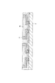
図1はこの発明の第1実施形態としての半導体装置の断面図を示す。この半導体装置は平面方形状のベース板(ベース部材)1を備えている。ベース板1は、通常、プリプレグ材と言われるもので、例えば、ガラス繊維やアラミド繊維等からなる基材にエポキシ系樹脂等の熱硬化性樹脂を含浸させたものからなっている。
図22はこの発明の第2実施形態としての半導体装置の断面図を示す。この半導体装置において、図1に示す場合と異なる点は、最下層絶縁膜43下に複数の半導体構成体(電子部品)71を搭載した点である。すなわち、第2の下層配線42の接続パッド部に対応する部分における最下層絶縁膜43には開口部44が設けられている。最下層絶縁膜43の下面には複数の半導体構成体71が、その上面に設けられた半田ボール72が最下層絶縁膜43の開口部44を介して第2の下層配線42の接続パッド部に接続されて、搭載されている。
上記実施形態では、配線板13として、多層配線板を用い、例えば、プリプレグ材からなる第1〜第3の絶縁基板を積層してなるものを用いた場合について説明したが、これに限らず、例えば、スルーホールメッキ導通部を有する両面配線構造のものを用いてもよい。
2 半導体構成体
3 シリコン基板
4 接続パッド
10 配線
11 柱状電極
12 封止膜
13 配線板
25 第1の上層絶縁膜
28 第1の上層配線
29 第2の上層絶縁膜
32 第2の上層配線
33 最上層絶縁膜
35 半田ボール
38 第1の下層配線
39 下層絶縁膜
42 第2の下層配線
43 最下層絶縁膜
Claims (8)
- 上面に端子が露出され前記端子間に絶縁層が設けられた集合配線板を有し、
各々が半導体基板および該半導体基板上に設けられた複数の外部接続用電極を有する複数の半導体構成体と前記各半導体構成体に対応する部分に開口部を有する前記集合配線板とを、前記集合配線板の各開口部内に前記半導体構成体が配置されるようにベース部材上に配置する工程と、
前記半導体構成体および前記集合配線板上に、接続パッド部を有する少なくとも1層の上層配線を前記半導体構成体の外部接続用電極および前記配線板に電気的に接続させて形成する工程と、
前記半導体構成体間における前記ベース部材および前記集合配線板を少なくとも切断して前記半導体構成体が少なくとも1つ含まれる半導体装置を複数個得る工程と、
を有し、
前記集合配線板および前記半導体構成体の上面に上層絶縁膜を配置し、加熱加圧板により前記上層絶縁膜を加熱加圧する工程を含む
ことを特徴とする半導体装置の製造方法。 - 請求項1に記載の発明において、前記集合配線板の各開口部内に前記半導体構成体を配置する工程は、前記集合配線板の各開口部と前記各半導体構成体との間に隙間が形成されるように配置し、前記隙間に充填材を充填する工程を含むことを特徴とする半導体装置の製造方法。
- 請求項1に記載の発明において、前記最上層の上層配線の接続パッド部の少なくとも一部を前記集合配線板上に配置することを特徴とする半導体装置の製造方法。
- 請求項1に記載の発明において、前記ベース部材はプリプレグ材からなることを特徴とする半導体装置の製造方法。
- 請求項1に記載の発明において、前記集合配線板は多層配線板からなることを特徴とする半導体装置の製造方法。
- 請求項1に記載の発明において、前記切断は、前記半導体構成体が複数個含まれるように切断することを特徴とする半導体装置の製造方法。
- 請求項1に記載の発明において、前記半導体構成体の前記ベース部材上への配置は、切断前の前記集合配線板の開口部の周囲における配線形成部が良品と判定された部分に対応する位置にのみ配置することを特徴とする半導体装置の製造方法。
- 請求項7に記載の発明において、切断前の前記集合配線板の開口部のうち、前記半導体構成体が配置されない開口部内に充填材を充填することを特徴とする半導体装置の製造方法。
Priority Applications (1)
| Application Number | Priority Date | Filing Date | Title |
|---|---|---|---|
| JP2003398540A JP4324732B2 (ja) | 2003-11-28 | 2003-11-28 | 半導体装置の製造方法 |
Applications Claiming Priority (1)
| Application Number | Priority Date | Filing Date | Title |
|---|---|---|---|
| JP2003398540A JP4324732B2 (ja) | 2003-11-28 | 2003-11-28 | 半導体装置の製造方法 |
Publications (2)
| Publication Number | Publication Date |
|---|---|
| JP2005159199A JP2005159199A (ja) | 2005-06-16 |
| JP4324732B2 true JP4324732B2 (ja) | 2009-09-02 |
Family
ID=34723359
Family Applications (1)
| Application Number | Title | Priority Date | Filing Date |
|---|---|---|---|
| JP2003398540A Expired - Fee Related JP4324732B2 (ja) | 2003-11-28 | 2003-11-28 | 半導体装置の製造方法 |
Country Status (1)
| Country | Link |
|---|---|
| JP (1) | JP4324732B2 (ja) |
Families Citing this family (7)
| Publication number | Priority date | Publication date | Assignee | Title |
|---|---|---|---|---|
| JP5042762B2 (ja) * | 2007-09-27 | 2012-10-03 | 株式会社テラミクロス | 半導体装置 |
| KR101161061B1 (ko) | 2007-08-08 | 2012-07-02 | 가부시키가이샤 테라미크로스 | 반도체 장치 제조방법 |
| JP2009182202A (ja) * | 2008-01-31 | 2009-08-13 | Casio Comput Co Ltd | 半導体装置の製造方法 |
| KR101015704B1 (ko) | 2008-12-01 | 2011-02-22 | 삼성전기주식회사 | 칩 내장 인쇄회로기판 및 그 제조방법 |
| JP5563814B2 (ja) * | 2009-12-18 | 2014-07-30 | 新光電気工業株式会社 | 半導体装置及びその製造方法 |
| JP5548060B2 (ja) | 2010-07-28 | 2014-07-16 | 株式会社東芝 | 半導体装置 |
| KR20120026855A (ko) | 2010-09-10 | 2012-03-20 | 삼성전기주식회사 | 임베디드 볼 그리드 어레이 기판 및 그 제조 방법 |
Family Cites Families (7)
| Publication number | Priority date | Publication date | Assignee | Title |
|---|---|---|---|---|
| JP3213292B2 (ja) * | 1999-07-12 | 2001-10-02 | ソニーケミカル株式会社 | 多層基板、及びモジュール |
| JP3619395B2 (ja) * | 1999-07-30 | 2005-02-09 | 京セラ株式会社 | 半導体素子内蔵配線基板およびその製造方法 |
| JP2001100871A (ja) * | 1999-10-04 | 2001-04-13 | Sharp Corp | テレビジョン受信機能を有するパーソナルコンピュータ |
| JP3813402B2 (ja) * | 2000-01-31 | 2006-08-23 | 新光電気工業株式会社 | 半導体装置の製造方法 |
| JP2002016173A (ja) * | 2000-06-30 | 2002-01-18 | Mitsubishi Electric Corp | 半導体装置 |
| JP2002270712A (ja) * | 2001-03-14 | 2002-09-20 | Sony Corp | 半導体素子内蔵多層配線基板と半導体素子内蔵装置、およびそれらの製造方法 |
| JP3870778B2 (ja) * | 2001-12-20 | 2007-01-24 | ソニー株式会社 | 素子内蔵基板の製造方法および素子内蔵基板 |
-
2003
- 2003-11-28 JP JP2003398540A patent/JP4324732B2/ja not_active Expired - Fee Related
Also Published As
| Publication number | Publication date |
|---|---|
| JP2005159199A (ja) | 2005-06-16 |
Similar Documents
| Publication | Publication Date | Title |
|---|---|---|
| JP3925809B2 (ja) | 半導体装置およびその製造方法 | |
| JP4055717B2 (ja) | 半導体装置およびその製造方法 | |
| KR100987688B1 (ko) | 프린트 배선 기판 및 프린트 배선 기판의 제조 방법 | |
| KR100595889B1 (ko) | 상하도전층의 도통부를 갖는 반도체장치 및 그 제조방법 | |
| JP3961537B2 (ja) | 半導体搭載用配線基板の製造方法、及び半導体パッケージの製造方法 | |
| JP4361826B2 (ja) | 半導体装置 | |
| JP4093186B2 (ja) | 半導体装置の製造方法 | |
| JP2006173232A (ja) | 半導体装置およびその製造方法 | |
| JP2004335641A (ja) | 半導体素子内蔵基板の製造方法 | |
| KR20060069231A (ko) | 다단구성의 반도체모듈 및 그 제조방법 | |
| US20080116562A1 (en) | Carrier structure for semiconductor chip and method for manufacturing the same | |
| JP4157829B2 (ja) | 半導体装置およびその製造方法 | |
| JP4950743B2 (ja) | 積層配線基板及びその製造方法 | |
| JP5238182B2 (ja) | 積層配線基板の製造方法 | |
| JP4324732B2 (ja) | 半導体装置の製造方法 | |
| JP4438389B2 (ja) | 半導体装置の製造方法 | |
| JP2009146940A (ja) | 積層配線基板及びその製造方法 | |
| JP2007096337A (ja) | 半導体搭載用配線基板、半導体パッケージ、及びその製造方法 | |
| JP2009004813A (ja) | 半導体搭載用配線基板 | |
| JP5285385B2 (ja) | 積層配線基板の製造方法 | |
| JP4321758B2 (ja) | 半導体装置 | |
| JP4429280B2 (ja) | 半導体搭載用配線基板の製造方法、及び半導体装置の製造方法 | |
| TWI420989B (zh) | 印刷電路板及其製造方法 | |
| JP4561079B2 (ja) | 半導体装置の製造方法 | |
| JP2007134739A (ja) | 半導体装置の製造方法 |
Legal Events
| Date | Code | Title | Description |
|---|---|---|---|
| RD02 | Notification of acceptance of power of attorney |
Free format text: JAPANESE INTERMEDIATE CODE: A7422 Effective date: 20060209 |
|
| RD04 | Notification of resignation of power of attorney |
Free format text: JAPANESE INTERMEDIATE CODE: A7424 Effective date: 20060404 |
|
| A621 | Written request for application examination |
Free format text: JAPANESE INTERMEDIATE CODE: A621 Effective date: 20061114 |
|
| A977 | Report on retrieval |
Free format text: JAPANESE INTERMEDIATE CODE: A971007 Effective date: 20080519 |
|
| RD04 | Notification of resignation of power of attorney |
Free format text: JAPANESE INTERMEDIATE CODE: A7424 Effective date: 20080519 |
|
| A131 | Notification of reasons for refusal |
Free format text: JAPANESE INTERMEDIATE CODE: A131 Effective date: 20080527 |
|
| A521 | Request for written amendment filed |
Free format text: JAPANESE INTERMEDIATE CODE: A523 Effective date: 20080725 |
|
| A131 | Notification of reasons for refusal |
Free format text: JAPANESE INTERMEDIATE CODE: A131 Effective date: 20081021 |
|
| A521 | Request for written amendment filed |
Free format text: JAPANESE INTERMEDIATE CODE: A523 Effective date: 20081216 |
|
| TRDD | Decision of grant or rejection written | ||
| A01 | Written decision to grant a patent or to grant a registration (utility model) |
Free format text: JAPANESE INTERMEDIATE CODE: A01 Effective date: 20090512 |
|
| A01 | Written decision to grant a patent or to grant a registration (utility model) |
Free format text: JAPANESE INTERMEDIATE CODE: A01 |
|
| A61 | First payment of annual fees (during grant procedure) |
Free format text: JAPANESE INTERMEDIATE CODE: A61 Effective date: 20090525 |
|
| FPAY | Renewal fee payment (event date is renewal date of database) |
Free format text: PAYMENT UNTIL: 20120619 Year of fee payment: 3 |
|
| R150 | Certificate of patent or registration of utility model |
Free format text: JAPANESE INTERMEDIATE CODE: R150 |
|
| FPAY | Renewal fee payment (event date is renewal date of database) |
Free format text: PAYMENT UNTIL: 20120619 Year of fee payment: 3 |
|
| FPAY | Renewal fee payment (event date is renewal date of database) |
Free format text: PAYMENT UNTIL: 20120619 Year of fee payment: 3 |
|
| S111 | Request for change of ownership or part of ownership |
Free format text: JAPANESE INTERMEDIATE CODE: R313111 |
|
| FPAY | Renewal fee payment (event date is renewal date of database) |
Free format text: PAYMENT UNTIL: 20120619 Year of fee payment: 3 |
|
| R350 | Written notification of registration of transfer |
Free format text: JAPANESE INTERMEDIATE CODE: R350 |
|
| FPAY | Renewal fee payment (event date is renewal date of database) |
Free format text: PAYMENT UNTIL: 20130619 Year of fee payment: 4 |
|
| FPAY | Renewal fee payment (event date is renewal date of database) |
Free format text: PAYMENT UNTIL: 20130619 Year of fee payment: 4 |
|
| R250 | Receipt of annual fees |
Free format text: JAPANESE INTERMEDIATE CODE: R250 |
|
| R250 | Receipt of annual fees |
Free format text: JAPANESE INTERMEDIATE CODE: R250 |
|
| R250 | Receipt of annual fees |
Free format text: JAPANESE INTERMEDIATE CODE: R250 |
|
| S111 | Request for change of ownership or part of ownership |
Free format text: JAPANESE INTERMEDIATE CODE: R313111 |
|
| R350 | Written notification of registration of transfer |
Free format text: JAPANESE INTERMEDIATE CODE: R350 |
|
| LAPS | Cancellation because of no payment of annual fees |