JP4324732B2 - Manufacturing method of semiconductor device - Google Patents
Manufacturing method of semiconductor device Download PDFInfo
- Publication number
- JP4324732B2 JP4324732B2 JP2003398540A JP2003398540A JP4324732B2 JP 4324732 B2 JP4324732 B2 JP 4324732B2 JP 2003398540 A JP2003398540 A JP 2003398540A JP 2003398540 A JP2003398540 A JP 2003398540A JP 4324732 B2 JP4324732 B2 JP 4324732B2
- Authority
- JP
- Japan
- Prior art keywords
- wiring
- wiring board
- semiconductor
- opening
- semiconductor structure
- Prior art date
- Legal status (The legal status is an assumption and is not a legal conclusion. Google has not performed a legal analysis and makes no representation as to the accuracy of the status listed.)
- Expired - Fee Related
Links
Images


Classifications
-
- H—ELECTRICITY
- H01—ELECTRIC ELEMENTS
- H01L—SEMICONDUCTOR DEVICES NOT COVERED BY CLASS H10
- H01L24/00—Arrangements for connecting or disconnecting semiconductor or solid-state bodies; Methods or apparatus related thereto
- H01L24/01—Means for bonding being attached to, or being formed on, the surface to be connected, e.g. chip-to-package, die-attach, "first-level" interconnects; Manufacturing methods related thereto
- H01L24/18—High density interconnect [HDI] connectors; Manufacturing methods related thereto
- H01L24/19—Manufacturing methods of high density interconnect preforms
-
- H—ELECTRICITY
- H01—ELECTRIC ELEMENTS
- H01L—SEMICONDUCTOR DEVICES NOT COVERED BY CLASS H10
- H01L2224/00—Indexing scheme for arrangements for connecting or disconnecting semiconductor or solid-state bodies and methods related thereto as covered by H01L24/00
- H01L2224/01—Means for bonding being attached to, or being formed on, the surface to be connected, e.g. chip-to-package, die-attach, "first-level" interconnects; Manufacturing methods related thereto
- H01L2224/10—Bump connectors; Manufacturing methods related thereto
- H01L2224/12—Structure, shape, material or disposition of the bump connectors prior to the connecting process
- H01L2224/12105—Bump connectors formed on an encapsulation of the semiconductor or solid-state body, e.g. bumps on chip-scale packages
-
- H—ELECTRICITY
- H01—ELECTRIC ELEMENTS
- H01L—SEMICONDUCTOR DEVICES NOT COVERED BY CLASS H10
- H01L2224/00—Indexing scheme for arrangements for connecting or disconnecting semiconductor or solid-state bodies and methods related thereto as covered by H01L24/00
- H01L2224/01—Means for bonding being attached to, or being formed on, the surface to be connected, e.g. chip-to-package, die-attach, "first-level" interconnects; Manufacturing methods related thereto
- H01L2224/10—Bump connectors; Manufacturing methods related thereto
- H01L2224/15—Structure, shape, material or disposition of the bump connectors after the connecting process
- H01L2224/16—Structure, shape, material or disposition of the bump connectors after the connecting process of an individual bump connector
- H01L2224/161—Disposition
- H01L2224/16151—Disposition the bump connector connecting between a semiconductor or solid-state body and an item not being a semiconductor or solid-state body, e.g. chip-to-substrate, chip-to-passive
- H01L2224/16221—Disposition the bump connector connecting between a semiconductor or solid-state body and an item not being a semiconductor or solid-state body, e.g. chip-to-substrate, chip-to-passive the body and the item being stacked
- H01L2224/16225—Disposition the bump connector connecting between a semiconductor or solid-state body and an item not being a semiconductor or solid-state body, e.g. chip-to-substrate, chip-to-passive the body and the item being stacked the item being non-metallic, e.g. insulating substrate with or without metallisation
-
- H—ELECTRICITY
- H01—ELECTRIC ELEMENTS
- H01L—SEMICONDUCTOR DEVICES NOT COVERED BY CLASS H10
- H01L2224/00—Indexing scheme for arrangements for connecting or disconnecting semiconductor or solid-state bodies and methods related thereto as covered by H01L24/00
- H01L2224/01—Means for bonding being attached to, or being formed on, the surface to be connected, e.g. chip-to-package, die-attach, "first-level" interconnects; Manufacturing methods related thereto
- H01L2224/18—High density interconnect [HDI] connectors; Manufacturing methods related thereto
- H01L2224/19—Manufacturing methods of high density interconnect preforms
-
- H—ELECTRICITY
- H01—ELECTRIC ELEMENTS
- H01L—SEMICONDUCTOR DEVICES NOT COVERED BY CLASS H10
- H01L2224/00—Indexing scheme for arrangements for connecting or disconnecting semiconductor or solid-state bodies and methods related thereto as covered by H01L24/00
- H01L2224/73—Means for bonding being of different types provided for in two or more of groups H01L2224/10, H01L2224/18, H01L2224/26, H01L2224/34, H01L2224/42, H01L2224/50, H01L2224/63, H01L2224/71
- H01L2224/732—Location after the connecting process
- H01L2224/73251—Location after the connecting process on different surfaces
- H01L2224/73267—Layer and HDI connectors
-
- H—ELECTRICITY
- H01—ELECTRIC ELEMENTS
- H01L—SEMICONDUCTOR DEVICES NOT COVERED BY CLASS H10
- H01L2224/00—Indexing scheme for arrangements for connecting or disconnecting semiconductor or solid-state bodies and methods related thereto as covered by H01L24/00
- H01L2224/91—Methods for connecting semiconductor or solid state bodies including different methods provided for in two or more of groups H01L2224/80 - H01L2224/90
- H01L2224/92—Specific sequence of method steps
- H01L2224/922—Connecting different surfaces of the semiconductor or solid-state body with connectors of different types
- H01L2224/9222—Sequential connecting processes
- H01L2224/92242—Sequential connecting processes the first connecting process involving a layer connector
- H01L2224/92244—Sequential connecting processes the first connecting process involving a layer connector the second connecting process involving a build-up interconnect
-
- H—ELECTRICITY
- H01—ELECTRIC ELEMENTS
- H01L—SEMICONDUCTOR DEVICES NOT COVERED BY CLASS H10
- H01L2924/00—Indexing scheme for arrangements or methods for connecting or disconnecting semiconductor or solid-state bodies as covered by H01L24/00
- H01L2924/10—Details of semiconductor or other solid state devices to be connected
- H01L2924/11—Device type
- H01L2924/14—Integrated circuits
-
- H—ELECTRICITY
- H01—ELECTRIC ELEMENTS
- H01L—SEMICONDUCTOR DEVICES NOT COVERED BY CLASS H10
- H01L2924/00—Indexing scheme for arrangements or methods for connecting or disconnecting semiconductor or solid-state bodies as covered by H01L24/00
- H01L2924/15—Details of package parts other than the semiconductor or other solid state devices to be connected
- H01L2924/151—Die mounting substrate
- H01L2924/153—Connection portion
- H01L2924/1531—Connection portion the connection portion being formed only on the surface of the substrate opposite to the die mounting surface
- H01L2924/15311—Connection portion the connection portion being formed only on the surface of the substrate opposite to the die mounting surface being a ball array, e.g. BGA
Description
この発明は半導体装置の製造方法に関する。 This invention relates to a method of manufacturing a semiconductor equipment.
近年、携帯電話に代表されるような携帯型電子機器の小型化に相俟ってCSP(chip size package)と呼ばれる半導体装置が開発されている。このCSPは、複数の外部接続用の接続パッドが形成されたベアーの半導体装置の上面にパッシベーション膜(中間絶縁膜)を設け、このパッシベーション膜の各接続パッドの対応部に開口部を形成し、該開口部を介して各接続パッドに接続される配線を形成し、各配線の他端部側に柱状の外部接続用電極を形成するとともに、各外部接続用電極間に封止材を充填したものである。 In recent years, a semiconductor device called a CSP (chip size package) has been developed in conjunction with downsizing of a portable electronic device represented by a mobile phone. This CSP is provided with a passivation film (intermediate insulating film) on the upper surface of a bare semiconductor device in which a plurality of connection pads for external connection are formed, and an opening is formed in a corresponding portion of each connection pad of the passivation film. A wiring connected to each connection pad is formed through the opening, a columnar external connection electrode is formed on the other end side of each wiring, and a sealing material is filled between each external connection electrode Is.
このような、CSPによれば、各柱状の外部接続用電極上に半田ボールを形成しておくことにより、接続端子を有する回路基板にフェースダウン方式でボンディングすることができ、実装面積をほぼベアーの半導体装置と同一のサイズとすることが可能となるので、従来のワイヤーボンディング等を用いたフェースアップ方式のボンディング方法に比し、電子機器を大幅に小型化することが可能である。 According to such CSP, by forming solder balls on each columnar external connection electrode, it is possible to bond to a circuit board having connection terminals by a face-down method, and the mounting area is almost bare. Therefore, the electronic device can be significantly reduced in size as compared with a conventional face-up bonding method using wire bonding or the like.
このような、CSPにおいて、生産性を高めるために、ウエハ状態の半導体基板にパッシベーション膜、配線、外部接続用電極、および封止材を形成し、さらに、封止材で覆われずに露出された外部接続用電極の上面に半田ボールを設けた後、ダイシングラインで切断するようにしたものがある(例えば、特許文献1参照)。 In such a CSP, in order to increase productivity, a passivation film, wiring, external connection electrodes, and a sealing material are formed on a semiconductor substrate in a wafer state, and further exposed without being covered with the sealing material. In some cases, a solder ball is provided on the upper surface of the external connection electrode and then cut by a dicing line (see, for example, Patent Document 1).
ところで、上記従来の半導体装置では、集積化が進むに従って、外部接続用電極の数が増加すると、次のような問題があった。すなわち、上述した如く、CSPは、ベアーの半導体装置の上面に外部接続用電極を配列するので、通常は、マトリクス状に配列するのであるが、そのために、外部接続用電極数の多い半導体装置の場合には、外部接続用電極のサイズおよびピッチが極端に小さくなってしまう欠点を有しており、このため、ベアーの半導体装置のサイズの割に外部接続用電極が多いものには適用できないものであった。 By the way, the conventional semiconductor device has the following problems when the number of external connection electrodes increases as integration proceeds. That is, as described above, since the CSP has the external connection electrodes arranged on the upper surface of the bare semiconductor device, the CSP is usually arranged in a matrix. For this reason, the CSP has a large number of external connection electrodes. In some cases, the size and pitch of the external connection electrodes are extremely small, so that the external connection electrodes cannot be applied to those having a large number of external connection electrodes for the size of the bare semiconductor device. Met.
すなわち、外部接続用電極のサイズおよびピッチが極端に小さくなれば、回路基板との位置合わせが困難であるばかりでなく、接合強度が不足する、ボンディング時に電極間の短絡が発生する、通常はシリコン基板からなる半導体基板と回路基板の線膨張係数の差に起因して発生する応力により外部接続用電極が破壊される等の致命的な問題が発生するのである。 That is, if the size and pitch of the electrodes for external connection become extremely small, not only alignment with the circuit board is difficult, but also the bonding strength is insufficient, and a short circuit between the electrodes occurs during bonding, usually silicon A fatal problem such as destruction of the external connection electrode occurs due to the stress generated due to the difference between the linear expansion coefficients of the semiconductor substrate and the circuit board.
また、上記従来の半導体装置では、上述の如く、回路基板にフェースダウン方式でボンディングすることができ、実装面積をほぼベアーの半導体装置と同一のサイズとすることが可能となるので、従来のワイヤーボンディング等を用いたフェースアップ方式のボンディング方法に比し、電子機器を大幅に小型化することが可能であるが、それでも小型化に限界があった。 Further, in the conventional semiconductor device, as described above, it can be bonded to the circuit board in a face-down manner, and the mounting area can be made almost the same size as the bare semiconductor device. Compared to the face-up type bonding method using bonding or the like, the electronic device can be greatly downsized, but there is still a limit to downsizing.
すなわち、回路基板に他の必要な電子部品、例えば、他の半導体装置、コンデンサや抵抗等のチップ部品を搭載し、これらの電子部品に上記従来の半導体装置を接続すると、これらが平面的に配置されるため、小型化に限界があった。また、平面的に配置される関係から、配線長が増大し、インピーダンス(浮遊容量等)の増加等の問題が生じ、回路特性が劣化することがあった。 That is, when other necessary electronic components such as other semiconductor devices, chip components such as capacitors and resistors are mounted on the circuit board, and the conventional semiconductor device is connected to these electronic components, these are arranged in a plane. Therefore, there was a limit to miniaturization. In addition, due to the planar arrangement, the wiring length increases, causing problems such as an increase in impedance (such as stray capacitance), and circuit characteristics may deteriorate.
そこで、この発明は、外部接続用電極の数が増加しても、そのサイズおよびピッチを必要な大きさにすることが可能となり、且つ、電子機器のより一層の小型化が可能で、配線長を最短として回路特性劣化を抑制することが可能となる新規な半導体装置およびその製造方法を提供することを目的とする。 Therefore, even if the number of external connection electrodes increases, the present invention makes it possible to make the size and pitch necessary, and to further reduce the size of the electronic device, and to increase the wiring length. It is an object of the present invention to provide a novel semiconductor device and a method of manufacturing the same that can suppress deterioration of circuit characteristics.
請求項1に記載の発明は、上面に端子が露出され前記端子間に絶縁層が設けられた集合配線板を有し、各々が半導体基板および該半導体基板上に設けられた複数の外部接続用電極を有する複数の半導体構成体と前記各半導体構成体に対応する部分に開口部を有する前記集合配線板とを、前記集合配線板の各開口部内に前記半導体構成体が配置されるようにベース部材上に配置する工程と、前記半導体構成体および前記集合配線板上に、接続パッド部を有する少なくとも1層の上層配線を前記半導体構成体の外部接続用電極および前記配線板に電気的に接続させて形成する工程と、前記半導体構成体間における前記ベース部材および前記集合配線板を少なくとも切断して前記半導体構成体が少なくとも1つ含まれる半導体装置を複数個得る工程と、を有し、前記集合配線板および前記半導体構成体の上面に上層絶縁膜を配置し、加熱加圧板により前記上層絶縁膜を加熱加圧する工程を含むことを特徴とするものである。
請求項2に記載の発明は、請求項1に記載の発明において、前記集合配線板の各開口部内に前記半導体構成体を配置する工程は、前記集合配線板の各開口部と前記各半導体構成体との間に隙間が形成されるように配置し、前記隙間に充填材を充填する工程を含むことを特徴とするものである。
請求項3に記載の発明は、請求項1に記載の発明において、前記最上層の上層配線の接続パッド部の少なくとも一部を前記集合配線板上に配置することを特徴とするものである。
請求項4に記載の発明は、請求項1に記載の発明において、前記ベース部材はプリプレグ材からなることを特徴とするものである。
請求項5に記載の発明は、請求項1に記載の発明において、前記集合配線板は多層配線板からなることを特徴とするものである。
請求項6に記載の発明は、請求項1に記載の発明において、前記切断は、前記半導体構成体が複数個含まれるように切断することを特徴とするものである。
請求項7に記載の発明は、請求項1に記載の発明において、前記半導体構成体の前記ベース部材上への配置は、切断前の前記集合配線板の開口部の周囲における配線形成部が良品と判定された部分に対応する位置にのみ配置することを特徴とするものである。
請求項8に記載の発明は、請求項7に記載の発明において、切断前の前記集合配線板の開口部のうち、前記半導体構成体が配置されない開口部内に充填材を充填することを特徴とするものである。
The invention according to
According to a second aspect of the present invention, in the first aspect of the present invention, the step of disposing the semiconductor structure in each opening of the collective wiring board includes the opening of the collective wiring board and the semiconductor structure. It arrange | positions so that a clearance gap may be formed between bodies, and the process of filling the said clearance gap with a filler is characterized by the above-mentioned.
According to a third aspect of the present invention, in the first aspect of the present invention, at least a part of the connection pad portion of the uppermost layer upper layer wiring is arranged on the collective wiring board.
The invention according to
According to a fifth aspect of the present invention, in the first aspect of the present invention, the collective wiring board is a multilayer wiring board.
According to a sixth aspect of the present invention, in the first aspect of the present invention, the cutting is performed so as to include a plurality of the semiconductor structural bodies.
According to a seventh aspect of the present invention, in the first aspect of the present invention, the semiconductor structure is arranged on the base member so that the wiring forming portion around the opening of the assembly wiring board before cutting is a non-defective product. It arrange | positions only in the position corresponding to the part determined to be.
The invention according to claim 8 is characterized in that, in the invention according to
この発明によれば、半導体構成体の周囲におけるベース部材上に配線板を設けているので、配線板上に最上層の上層配線の少なくとも一部の接続パッドを配置するようにして、最上層の上層配線の接続パッド部(外部接続用電極)の数が増加しても、そのサイズおよびピッチを必要な大きさにすることが可能となる。また、ベース部材下に少なくとも1層の下層配線を配線板に電気的に接続させて設けているので、最下層の下層配線に電子部品を接続させて搭載するようにして、電子機器のより一層の小型化が可能で、且つ、配線長を最短として回路特性を向上させることが可能となる。 According to the present invention, since the wiring board is provided on the base member around the semiconductor structure, at least a part of the connection pads of the uppermost upper layer wiring is arranged on the wiring board so that the uppermost layer is formed. Even if the number of connection pad portions (external connection electrodes) of the upper layer wiring is increased, it is possible to make the size and pitch necessary. In addition, since at least one lower layer wiring is electrically connected to the wiring board under the base member, an electronic component is connected to and mounted on the lowermost lower layer wiring so that the electronic device can be further connected. The circuit characteristics can be improved with the wiring length as short as possible.
(第1実施形態)
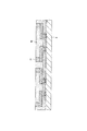
図1はこの発明の第1実施形態としての半導体装置の断面図を示す。この半導体装置は平面方形状のベース板(ベース部材)1を備えている。ベース板1は、通常、プリプレグ材と言われるもので、例えば、ガラス繊維やアラミド繊維等からなる基材にエポキシ系樹脂等の熱硬化性樹脂を含浸させたものからなっている。
(First embodiment)
FIG. 1 is a sectional view of a semiconductor device as a first embodiment of the present invention. This semiconductor device includes a planar rectangular base plate (base member) 1. The
ベース板1の上面には、ベース板1のサイズよりもある程度小さいサイズの平面方形状の半導体構成体2の下面が固着されている。この場合、半導体構成体2は、後述する配線、柱状電極、封止膜を有しており、一般的にはCSP(chip size package)と呼ばれるものであり、特に、後述の如く、シリコンウエハ上に配線、柱状電極、封止膜を形成した後、ダイシングにより個々の半導体構成体2を得る方法を採用しているため、特に、ウエハレベルCSP(W−CSP)とも言われている。以下に、半導体構成体2の構成について説明する。
On the upper surface of the
半導体構成体2は平面方形状のシリコン基板(半導体基板)3を備えている。シリコン基板3の下面はベース板1に固着されている。シリコン基板3の上面中央部には所定の機能の集積回路(図示せず)が設けられ、上面周辺部にはアルミニウム系金属等からなる複数の接続パッド4が集積回路に接続されて設けられている。
The
接続パッド4の中央部を除くシリコン基板3の上面には酸化シリコン等からなる絶縁膜5が設けられ、接続パッド4の中央部は絶縁膜5に設けられた開口部6を介して露出されている。絶縁膜5の上面にはエポキシ系樹脂やポリイミド系樹脂等からなる保護膜(絶縁膜)7が設けられている。この場合、絶縁膜5の開口部6に対応する部分における保護膜7には開口部8が設けられている。
An
保護膜7の上面には銅等からなる下地金属層9が設けられている。下地金属層9の上面全体には銅からなる配線10が設けられている。下地金属層9を含む配線10の一端部は、両開口部6、8を介して接続パッド4に接続されている。配線10の接続パッド部上面には銅からなる柱状電極11が設けられている。配線10を含む保護膜7の上面にはエポキシ系樹脂やポリイミド系樹脂等からなる封止膜12がその上面が柱状電極11の上面と面一となるように設けられている。
A
このように、W−CSPと呼ばれる半導体構成体2は、シリコン基板3、接続パッド4、絶縁膜5を含み、さらに、保護膜7、配線10、柱状電極11、封止膜12を含んで構成されている。
As described above, the
半導体構成体2の周囲におけるベース板1の上面には方形枠状の配線板13がその上面が半導体構成体2の上面とほぼ面一となるように設けられている。配線板13は、多層配線板からなり、例えば、第1の絶縁基板14の上下面に第2、第3の絶縁基板15、16が積層され、第2の絶縁基板15内に設けられたビア17と第3の絶縁基板16内に設けられたビア18とが、第1の絶縁基板14内に設けられたビア19および第1の絶縁基板14の上下面に設けられた上面配線20、下面配線21を介して接続された構造となっている。この場合、第1〜第3の絶縁基板14〜16はベース板1と同一の材料であるプリプレグ材からなっている。上面配線20および下面配線21は銅箔からなっている。
A rectangular frame-
配線板13には半導体構成体2よりもやや大きめの開口部22が設けられている。したがって、半導体構成体2と配線板13との間には隙間23が形成されている。この隙間23の間隔は、一例として、0.1〜0.5mmである。隙間23内には絶縁性の充填材24が充填されている。充填材24は、エポキシ系樹脂、ポリイミド系樹脂、アクリル系樹脂、ポリベンゾオキサゾール樹脂、カルゾ樹脂等の樹脂中に熱膨張係数低下用材料としての繊維やフィラーが混入されたものからなっている。この場合、繊維は、ガラス繊維やアラミド繊維等である。フィラーは、シリカフィラー等である。
The
半導体構成体2、充填材24および配線板13の上面には第1の上層絶縁膜25がその上面を平坦とされて設けられている。第1の上層絶縁膜25は、ビルドアップ基板に用いられる、通常、ビルドアップ材と言われるもので、例えば、エポキシ系樹脂やBT樹脂等の熱硬化性樹脂中に繊維やフィラー等の補強材が混入されたものからなっている。この場合、繊維は、ガラス繊維やアラミド繊維等である。フィラーは、シリカフィラー等である。
A first upper-
柱状電極11およびビア17の上面中央部に対応する部分における第1の上層絶縁膜25には開口部26が設けられている。第1の上層絶縁膜25の上面には銅等からなる第1の上層下地金属層27が設けられている。第1の上層下地金属層27の上面全体には銅からなる第1の上層配線28が設けられている。第1の上層下地金属層27を含む第1の上層配線28の一端部は、開口部26を介して柱状電極11またはビア17の上面に接続されている。
An
第1の上層配線28を含む第1の上層絶縁膜25の上面にはエポキシ系樹脂やポリイミド系樹脂等からなる第2の上層絶縁膜29が設けられている。第1の上層配線28の接続パッド部に対応する部分における第2の上層絶縁膜29には開口部30が設けられている。第2の上層絶縁膜29の上面には銅等からなる第2の上層下地金属層31が設けられている。第2の上層下地金属層31の上面全体には銅からなる第2の上層配線32が設けられている。第2の上層下地金属層31を含む第2の上層配線32の一端部は、開口部30を介して第1の上層配線28の接続パッド部に接続されている。
A second upper insulating
第2の上層配線32を含む第2の上層絶縁膜29の上面にはソルダーレジスト等からなる最上層絶縁膜33が設けられている。第2の上層配線32の接続パッド部に対応する部分における最上層絶縁膜33には開口部34が設けられている。開口部34内およびその上方には半田ボール35が第2の上層配線32の接続パッド部に接続されて設けられている。複数の半田ボール35は、最上層絶縁膜33の上面にマトリクス状に配置されている。
On the upper surface of the second upper
ビア18の下面中央部に対応する部分におけるベース板1には開口部36が設けられている。ベース板1の下面には銅等からなる第1の下層下地金属層37が設けられている。第1の下層下地金属層37の下面全体には銅からなる第1の下層配線38が設けられている。第1の下層下地金属層37を含む第1の下層配線38の一端部は、開口部36を介してビア18の下面に接続されている。
An
第1の下層配線38を含むベース板1の下面には第1の上層絶縁膜25と同一の材料からなる下層絶縁膜39が設けられている。第1の下層配線38の接続パッド部に対応する部分における下層絶縁膜39には開口部40が設けられている。下層絶縁膜39の下面には銅等からなる第2の下層下地金属層41が設けられている。第2の下層下地金属層41の下面全体には銅からなる第2の下層配線42が設けられている。第2の下層下地金属層41を含む第2の下層配線42の一端部は、開口部40を介して第1の下層配線38の接続パッド部に接続されている。第2の下層配線42を含む下層絶縁膜39の下面にはソルダーレジスト等からなる最下層絶縁膜43が設けられている。
A lower insulating
ところで、ベース板1のサイズを半導体構成体2のサイズよりもある程度大きくしているのは、シリコン基板3上の接続パッド4の数の増加に応じて、半田ボール35の配置領域を半導体構成体2のサイズよりもある程度大きくし、これにより、第2の上層配線32の接続パッド部(最上層絶縁膜33の開口部34内の部分)のサイズおよびピッチを柱状電極11のサイズおよびピッチよりも大きくするためである。
By the way, the size of the
このため、マトリクス状に配置された第2の上層配線32の接続パッド部は、半導体構成体2に対応する領域のみでなく、半導体構成体2の側面の外側に設けられた配線板13に対応する領域上にも配置されている。つまり、マトリクス状に配置された半田ボール35のうち、少なくとも最外周の半田ボール35は半導体構成体2よりも外側に位置する周囲に配置されている。
For this reason, the connection pad portion of the second
また、この半導体装置では、半導体構成体2の周囲におけるベース1板上に、樹脂中に熱膨張係数低下用材料が混入されたものからなる充填材24を設けているので、樹脂のみからなる充填材を設ける場合と比較して、半導体構成体2とその側面を覆っている絶縁層21との間に生じる応力を緩和することができる。この場合、充填材24の熱膨張係数は、半導体構成体2のシリコン基板2の熱膨張係数よりも大きく、且つ、配線板13の絶縁基板14〜16の熱膨張係数よりも小さくなっている。
Further, in this semiconductor device, since the
さらに、この半導体装置では、半導体構成体2の周囲におけるベース板1の上面に方形枠状の配線板13を設けているので、配線板13の代わりに単なる絶縁層を設けた場合と比較して、高密度配線構造とすることができる。すなわち、配線板13の代わりに単なる絶縁層を設けた場合には、当該絶縁層にスルーホールを形成して、上層配線28、32と下層配線38、42とをただ単に接続するだけとなり、高密度配線構造とすることはできない。なお、第2の絶縁基板15の上面および第3の絶縁基板16の下面に銅箔からなる配線をビア17、18に接続させて設けるようにしてもよい。
Further, in this semiconductor device, since the rectangular frame-
次に、この半導体装置の製造方法の一例について説明するに、まず、半導体構成体2の製造方法の一例について説明する。この場合、まず、図2に示すように、ウエハ状態のシリコン基板(半導体基板)3上にアルミニウム系金属等からなる接続パッド4、酸化シリコン等からなる絶縁膜5およびエポキシ系樹脂やポリイミド系樹脂等からなる保護膜7が設けられ、接続パッド4の中央部が絶縁膜5および保護膜7に形成された開口部6、8を介して露出されたものを用意する。上記において、ウエハ状態のシリコン基板3には、各半導体構成体が形成される領域に所定の機能の集積回路が形成され、接続パッド4は、それぞれ、対応する領域に形成された集積回路に電気的に接続されている。
Next, an example of a method for manufacturing the
次に、図3に示すように、両開口部6、8を介して露出された接続パッド4の上面を含む保護膜7の上面全体に下地金属層9を形成する。この場合、下地金属層9は、無電解メッキにより形成された銅層のみであってもよく、またスパッタにより形成された銅層のみであってもよく、さらにスパッタにより形成されたチタン等の薄膜層上にスパッタにより銅層を形成したものであってもよい。これは、後述する下地金属層27、31、37、41も同様である。
Next, as shown in FIG. 3, a
次に、下地金属層9の上面にメッキレジスト膜51をパターン形成する。この場合、配線10形成領域に対応する部分におけるメッキレジスト膜51には開口部52が形成されている。次に、下地金属層9をメッキ電流路として銅の電解メッキを行なうことにより、メッキレジスト膜51の開口部52内の下地金属層9の上面に配線10を形成する。次に、メッキレジスト膜51を剥離する。
Next, a plating resist
次に、図4に示すように、配線10を含む下地金属層9の上面にメッキレジスト膜53をパターン形成する。この場合、柱状電極11形成領域に対応する部分におけるメッキレジスト膜53には開口部54が形成されている。次に、下地金属層9をメッキ電流路として銅の電解メッキを行なうことにより、メッキレジスト膜53の開口部54内の配線10の接続パッド部上面に柱状電極11を形成する。次に、メッキレジスト膜53を剥離し、次いで、配線10をマスクとして下地金属層9の不要な部分をエッチングして除去すると、図5に示すように、配線10下にのみ下地金属層9が残存される。
Next, as shown in FIG. 4, a plating resist
次に、図6に示すように、スクリーン印刷法、スピンコーティング法、ダイコート法等により、柱状電極11および配線10を含む保護膜7の上面全体にエポキシ系樹脂やポリイミド系樹脂等からなる封止膜12をその厚さが柱状電極11の高さよりも厚くなるように形成する。したがって、この状態では、柱状電極11の上面は封止膜12によって覆われている。
Next, as shown in FIG. 6, the entire upper surface of the
次に、封止膜12および柱状電極11の上面側を適宜に研磨し、図7に示すように、柱状電極11の上面を露出させ、且つ、この露出された柱状電極11の上面を含む封止膜12の上面を平坦化する。ここで、柱状電極11の上面側を適宜に研磨するのは、電解メッキにより形成される柱状電極11の高さにばらつきがあるため、このばらつきを解消して、柱状電極11の高さを均一にするためである。
Next, the upper surface side of the sealing
次に、図8に示すように、バーンイン用検査治具55として、下面に配線(図示せず)を有する配線板56の下面側に複数のプローブピン57を有するプローブピン支持板58が配置され、プローブピン57の上端面が異方導電性ゴム59を介して配線板56の配線に接続されたものを用意する。この場合、プローブピン57の先端部はほぼ半球形状となっている。また、プローブピン57の直径は柱状電極11の直径よりもある程度小さくなっている。
Next, as shown in FIG. 8, a probe
そして、図示しないステージ上に配置されたウエハ状態のシリコン基板3上に形成された柱状電極11の上面に、バーンイン用検査治具55のプローブピン57の先端部を接触させ、バーンインを行なう。そして、このバーンインにより、ウエハ状態における各半導体装置の良否を判定する。次に、シリコン基板3をダイシングテープ(図示せず)に貼り付け、図9に示すダイシング工程を経た後に、ダイシングテープから剥がすと、図1に示す半導体構成体2が複数個得られる。そして、上記バーンインによる判定結果に基づいて、良品の半導体構成体2のみを選び出す。
Then, the tip end portion of the
次に、図1に示す配線板13の製造方法の一例について、簡単に説明する。まず、図10に示すように、上面配線20および下面配線21がビア19により導通されたプリプレグ材またはビルドアップ材からなる第1の絶縁基板14を用意する。この第1の絶縁基板14を形成するには、通常のビルドアッププリント基板の製造方法を用いればよく、フォトリソグラフィ技術またはレーザビームによりビアホールを形成し、めっきにより、あるいはスパッタ法とめっきにより、上面配線20、下面配線21およびビア19を形成する。ビア19は、導電ペーストをビアホールに充填する方法あるいは導電材料からなるピンを圧入する方法によってもよい。
Next, an example of a method for manufacturing the
次に、図11に示すように、上面配線20を含む第1の絶縁基板14の上面に、プリプレグ材またはビルドアップ材からなる第2の絶縁基板15を積層するとともに、下面配線21を含む第1の絶縁基板14の下面に、プリプレグ材またはビルドアップ材からなる第3の絶縁基板16を積層する。そして、第2の絶縁基板15にビア17を、また第3の絶縁基板16にビア18を、第1の絶縁基板14にビア19を形成する場合と同様な方法で形成する。図11においては、ビア17上とその周辺部、およびビア18上とその周縁部を覆う配線は形成されていないが、ビア17およびビア18を形成する際、このような配線を同時に形成してもよい。いずれにしても、図11に図示された状態で、ビア17は上面配線20の他端部に接続され、ビア18は下面配線21の他端部に接続されている。
Next, as shown in FIG. 11, a second insulating
ここで、第1〜第3の絶縁基板14〜16は、図1に示す配線板13を複数枚採取することができる大きさで、限定する意味ではないが、平面形状が方形状となっている。そして、次に、図12に示すように、パンチングにより、第1〜第3の絶縁基板14〜16に複数の方形状の開口部22を形成し、平面形状が格子状とされた第1〜第3の絶縁基板14〜16からなる集合配線板13aを形成する。次に、集合配線板13aに対して電気的検査を行ない、集合配線板13aにおける各配線板13形成領域の電気的良否を判定する。
Here, the first to third
次に、上記のようにして得られた良品の半導体構成体2および各配線板13形成領域の電気的良否判定済みの集合配線板13aを用いて、図1に示す半導体装置を製造する場合の一例について説明する。まず、図13に示すように、図1に示すベース板1を複数枚採取することができる大きさで、集合配線板13aに対応する大きさのプリプレグ材からなるベース板1を用意する。この場合、ベース板1を構成するプリプレグ材中のエポキシ系樹脂等からなる熱硬化性樹脂は、半硬化状態となっている。
Next, in the case of manufacturing the semiconductor device shown in FIG. 1 using the
次に、ベース板1の上面の所定の複数箇所にそれぞれ良品の半導体構成体2のシリコン基板3の下面を仮圧着する。すなわち、加熱機構付きのボンディングツール(図示せず)を用い、半導体装置2を、加熱した状態で一定の圧力をかけながら、プリプレグ材からなるベース板1の上面の所定の箇所に仮圧着する。仮圧着条件は、一例として、温度90〜130℃、圧力0.1〜1Mpaである。
Next, the lower surface of the
次に、半導体構成体2間および最外周に配置された半導体構成体2の外側におけるベース板1の上面に、集合配線板13aをピン等で位置決めしながら配置する。この状態では、集合配線板13aの開口部22のサイズは半導体構成体2のサイズよりもやや大きくなっているので、集合配線板13aの各開口部22と半導体構成体2との間には隙間23が形成されている。また、この状態では、集合配線板13aの上面と半導体構成体2の上面とはほぼ同一の平面上に配置されている。上記の工程において、ベース板1上に半導体構成体2および集合配線板13aを配置する順序は、逆でもよく、先に集合配線板13aを配置した後、この集合配線板13aの各開口部内22内に半導体構成体2を配置するようにしてもよい。
Next, the
ここで、集合配線板13aの各配線板13形成領域の電気的良否の判定は済んでいるので、良品と判定された配線板13形成領域の開口部22内にのみ半導体構成体2を配置し、不良品と判定された配線板13形成領域の開口部22内には半導体構成体2を配置しない。これにより、良品と判定された半導体構成体2の無駄を防止し、歩留の向上を図ることができる。
Here, since the determination of the electrical quality of each
次に、図14に示すように、隙間23内に樹脂中に熱膨張係数低下用材料が混入されたものからなるペースト状または粉末状の充填材24を印刷法等により充填する。この場合、不良品と判定された配線板13形成領域の開口部22内には半導体構成体2が配置されていないので、当該開口部22全領域内に充填材24を充填する。
Next, as shown in FIG. 14, a paste-like or powder-
次に、集合配線板13a、半導体構成体2および充填材24の上面に第1の上層絶縁膜25を形成するためのシート状のビルドアップ材を配置する。このビルドアップ材としては、エポキシ系樹脂等の熱硬化性樹脂中にシリカフィラーを混入させ、熱硬化性樹脂を半硬化状態にしたものがある。
Next, a sheet-like build-up material for forming the first upper insulating
次に、一対の加熱加圧板61、62を用いて上下からベース板1、充填材24および第1の上層絶縁膜25形成用のビルドアップ材を加熱加圧する。すると、ベース板1中の熱硬化性樹脂が硬化し、ベース板1の上面に半導体構成体2のシリコン基板3の下面および第3の絶縁基板16の下面が固着される。また、充填材24中の熱硬化性樹脂が硬化し、充填材24が半導体構成体2の側面、集合配線板13aの各開口部22の内壁面およびその間のベース板1の上面に固着される。さらに、ビルドアップ材中の熱硬化性樹脂が硬化し、半導体構成体2、充填材24および第2の絶縁基板15の上面に第1の上層絶縁膜25が形成される。
Next, the
この場合、第1の上層絶縁膜25の上面は、上側の加熱加圧板61の下面によって押さえ付けられるため、平坦面となる。また、ベース板1の下面は、下側の加熱加圧板62の上面によって押さえ付けられるため、平坦面となる。したがって、第1の上層絶縁膜25の上面およびベース板1の下面を平坦化するための研磨工程は不要である。このため、ベース板1のサイズが例えば500×500mm程度と比較的大きくても、その上に配置された複数の半導体構成体2に対して第1の上層絶縁膜25の上面およびベース板1の下面の平坦化を一括して簡単に行なうことができる。
In this case, since the upper surface of the first upper insulating
なお、ベース板1上に半導体構成体3および集合配線板13aを配置し、次いで、上下から加熱加圧し、次いで、印刷法等により隙間23内に充填材24を充填し、次いで、それらの上にビルドアップ材を配置し、次いで、上下から加熱加圧するようにしてもよい。また、ベース板1上に半導体構成体3および集合配線板13aを配置し、次いで、上下から加熱加圧し、次いで、印刷法等により隙間23内に充填材24を充填するとともにそれらの上に充填材24と同一の材料からなる第1の上層絶縁膜形成用層を形成し、次いで、上下から加熱加圧するようにしてもよい。
The
次に、図15に示すように、レーザビームを照射するレーザ加工により、柱状電極11およびビア17の上面中央部に対応する部分における第1の上層絶縁膜25に開口部26を形成する。また、ビア18の下面中央部に対応する部分におけるベース板1に開口部36を形成する。次に、必要に応じて、開口部26、36内等に発生したエポキシスミア等をデスミア処理により除去する。
Next, as shown in FIG. 15, an
次に、図16に示すように、開口部26を介して露出された柱状電極11およびビア17の上面を含む第1の上層絶縁膜25の上面全体および開口部36を介して露出されたビア18の下面を含むベース板1の下面全体に、銅の無電解メッキ等により、第1の上層下地金属層27および第1の下層下地金属層37を形成する。
Next, as shown in FIG. 16, the entire upper surface of the first upper insulating
次に、第1の上層下地金属層27の上面に上層メッキレジスト膜63をパターン形成し、また、第1の下層下地金属層37の下面に下層メッキレジスト膜64をパターン形成する。この場合、第1の上層配線28形成領域に対応する部分における上層メッキレジスト膜63には開口部65が形成されている。また、第1の下層配線38形成領域に対応する部分における下層メッキレジスト膜64には開口部66が形成されている。
Next, the upper plating resist
次に、下地金属層27、37をメッキ電流路として銅の電解メッキを行なうことにより、上層メッキレジスト膜63の開口部65内の第1の上層下地金属層27の上面に第1の上層配線28を形成し、また、下層メッキレジスト膜64の開口部66内の第1の下層下地金属層37の下面に第1の下層配線38を形成する。
Next, by performing copper electroplating using the base metal layers 27 and 37 as plating current paths, a first upper layer wiring is formed on the upper surface of the first upper layer
次に、両メッキレジスト膜63、64を剥離し、次いで、第1の上層配線28および第1の下層配線38をマスクとして第1の上層下地金属層27および第1の下層下地金属層37の不要な部分をエッチングして除去すると、図17に示すように、第1の上層配線28下にのみ第1の上層下地金属層27が残存され、また、第1の下層配線38上にのみ第1の下層下地金属層37が残存される。
Next, the plating resist
次に、図18に示すように、第1の上層配線28を含む第1の上層絶縁膜25の上面にシート状のビルドアップ材等からなる第2の上層絶縁膜29を形成し、また、第1の下層配線38を含むベース板1の下面にシート状のビルドアップ材等からなる下層絶縁膜39を形成する。
Next, as shown in FIG. 18, a second upper
次に、レーザビームを照射するレーザ加工により、第1の上層配線28の接続パッド部に対応する部分における第2の上層絶縁膜29に開口部30を形成し、また、第1の下層配線38の接続パッド部に対応する部分における下層絶縁膜39に開口部40を形成する。次に、必要に応じて、開口部30、40内等に発生したエポキシスミア等をデスミア処理により除去する。
Next, an
次に、図19に示すように、開口部30を介して露出された第1の上層配線28の接続パッド部を含む第2の上層絶縁膜29の上面全体および開口部40を介して露出された第1の下層配線38の接続パッド部を含む下層絶縁膜39の下面全体に、銅の無電解メッキ等により、第2の上層下地金属層31および第2の下層下地金属層41を形成する。
Next, as shown in FIG. 19, the entire upper surface of the second upper insulating
次に、第2の上層下地金属層31の上面に上層メッキレジスト膜67をパターン形成し、また、第2の下層下地金属層41の下面に下層メッキレジスト膜68をパターン形成する。この場合、第2の上層配線32形成領域に対応する部分における上層メッキレジスト膜67には開口部69が形成されている。また、第2の下層配線42形成領域に対応する部分における下層メッキレジスト膜68には開口部70が形成されている。
Next, the upper layer plating resist
次に、下地金属層31、41をメッキ電流路として銅の電解メッキを行なうことにより、上層メッキレジスト膜67の開口部69内の第2の上層下地金属層31の上面に第2の上層配線32を形成し、また、下層メッキレジスト膜68の開口部70内の第2の下層下地金属層41の下面に第2の下層配線42を形成する。
Next, the second upper layer wiring is formed on the upper surface of the second upper layer
次に、両メッキレジスト膜67、68を剥離し、次いで、第2の上層配線32および第2の下層配線42をマスクとして第2の上層下地金属層31および第2の下層下地金属層41の不要な部分をエッチングして除去すると、図20に示すように、第2の上層配線32下にのみ第2の上層下地金属層31が残存され、また、第2の下層配線42上にのみ第2の下層下地金属層41が残存される。
Next, the plating resist
次に、図21に示すように、スクリーン印刷法やスピンコーティング法等により、第2の上層配線32を含む第2の上層絶縁膜29の上面にソルダーレジスト等からなる最上層絶縁膜33を形成し、また、第2の下層配線42を含む下層絶縁膜39の下面にソルダーレジスト等からなる最下層絶縁膜43を形成する。この場合、第2の上層配線32の接続パッド部に対応する部分における最上層絶縁膜33には開口部34が形成されている。なお、第2の下層配線42の接続パッド部に対応する部分における最下層絶縁膜43には開口部は形成しない。したがって、第2の下層配線42の接続パッド部は最下層絶縁膜43によって覆われている。
Next, as shown in FIG. 21, an uppermost insulating
次に、開口部34内およびその上方に半田ボール35を第2の上層配線32の接続パッド部に接続させて形成する。次に、互いに隣接する半導体構成体2間において、最上層絶縁膜33、第2の上層絶縁膜29、第1の上層絶縁膜25、集合配線板13a、ベース板1、下層絶縁膜39および最下層絶縁膜43を切断すると、図1に示す半導体装置が複数個得られる。
Next, the
(第2実施形態)
図22はこの発明の第2実施形態としての半導体装置の断面図を示す。この半導体装置において、図1に示す場合と異なる点は、最下層絶縁膜43下に複数の半導体構成体(電子部品)71を搭載した点である。すなわち、第2の下層配線42の接続パッド部に対応する部分における最下層絶縁膜43には開口部44が設けられている。最下層絶縁膜43の下面には複数の半導体構成体71が、その上面に設けられた半田ボール72が最下層絶縁膜43の開口部44を介して第2の下層配線42の接続パッド部に接続されて、搭載されている。
(Second Embodiment)
FIG. 22 is a sectional view of a semiconductor device as a second embodiment of the present invention. This semiconductor device is different from the case shown in FIG. 1 in that a plurality of semiconductor components (electronic parts) 71 are mounted under the lowermost insulating
この場合、半導体構成体71は、詳細には図示していないが、ベアチップ、BGA(ball grid array)、CSP等のいずれであってもよく、シリコン等からなる半導体基板の上面には所定の機能の集積回路が設けられ、上面周辺部にはアルミニウム系金属等からなる複数の接続パッドが集積回路に接続されて設けられ、接続パッド自体または該接続パッドに接続された柱状電極等からなる外部接続用電極上に半田ボール72が設けられた構造となっている。
In this case, although not shown in detail, the
そして、この半導体装置では、ベース板下に第1、第2の下層配線38、42を配線板13のビア18に接続させて設け、最下層絶縁膜43下に半導体構成体71を第2の下層配線42の接続パッド部に接続させて搭載しているので、電子機器のより一層の小型化が可能になるとともに、配線長を最短として回路特性を向上させることができる。なお、最下層絶縁膜43下にコンデンサや抵抗等からなるチップ部品(電子部品)を搭載するようにしてもよい。
In this semiconductor device, the first and second
(その他の実施形態)
上記実施形態では、配線板13として、多層配線板を用い、例えば、プリプレグ材からなる第1〜第3の絶縁基板を積層してなるものを用いた場合について説明したが、これに限らず、例えば、スルーホールメッキ導通部を有する両面配線構造のものを用いてもよい。
(Other embodiments)
In the said embodiment, although the multilayer wiring board was used as the
また、上記実施形態では、上層配線および下層配線を共に2層とした場合について説明したが、これに限らず、1層または3層以上としてもよく、また、同数層ではなく異数層としてもよい。ただし、同数層とした場合には、半導体装置の反りを低減することができる。 In the above embodiment, the case where both the upper layer wiring and the lower layer wiring are two layers has been described. However, the present invention is not limited to this, and one layer or three or more layers may be used. Good. However, when the number of layers is the same, warpage of the semiconductor device can be reduced.
また、上記実施形態では、互いに隣接する半導体構成体2間において切断したが、これに限らず、2個またはそれ以上の半導体構成体2を1組として切断するようにしてもよい。この場合、複数で1組の半導体構成体2は同種、異種のいずれであってもよい。
Moreover, in the said embodiment, although it cut | disconnected between the mutually
また、上記実施形態では、半導体構成体2は、外部接続用電極としての柱状電極11を有するものとしたが、これに限らず、柱状電極を有せず、外部接続用電極としての接続パッド部を有する配線11を有するものであってもよく、また、柱状電極および配線を有せず、外部接続用電極としての接続パッド4を有するものであってもよい。
Moreover, in the said embodiment, although the
また、上記実施形態では、ベース板1としてプリプレグ材を用いた場合について説明したが、これに限らず、樹脂単体、シリコン、ガラス、セラミックス等の絶縁板を用いてもよい。ただし、このような絶縁板を用いる場合には、絶縁板の上面に半導体構成体2のシリコン基板3の下面および配線板13の下面を接着剤を介して接着するようにしてもよい。
Moreover, although the said embodiment demonstrated the case where a prepreg material was used as the
また、上記実施形態では、ベース板1は、そのまま半導体装置の構成部材の一部として残存されるものであるが、図14に図示された第1の上層絶縁膜25を形成した以降のいずれかの工程において、半導体構成体3から剥離し、接着、印刷、コーティング等適宜な方法により新たに形成するようにしてもよい。この場合、ベース板としての支持部材に剥離材を介して金属箔等からなる薄膜を形成し、第1の上層絶縁膜25を形成した後、支持部材を剥離し、薄膜のみを残したり、あるいは残存された薄膜上にさらに導電性あるいは絶縁性の支持用あるいは保護用の膜を形成してもよい。
Further, in the above embodiment, the
1 ベース板
2 半導体構成体
3 シリコン基板
4 接続パッド
10 配線
11 柱状電極
12 封止膜
13 配線板
25 第1の上層絶縁膜
28 第1の上層配線
29 第2の上層絶縁膜
32 第2の上層配線
33 最上層絶縁膜
35 半田ボール
38 第1の下層配線
39 下層絶縁膜
42 第2の下層配線
43 最下層絶縁膜
DESCRIPTION OF
Claims (8)
各々が半導体基板および該半導体基板上に設けられた複数の外部接続用電極を有する複数の半導体構成体と前記各半導体構成体に対応する部分に開口部を有する前記集合配線板とを、前記集合配線板の各開口部内に前記半導体構成体が配置されるようにベース部材上に配置する工程と、
前記半導体構成体および前記集合配線板上に、接続パッド部を有する少なくとも1層の上層配線を前記半導体構成体の外部接続用電極および前記配線板に電気的に接続させて形成する工程と、
前記半導体構成体間における前記ベース部材および前記集合配線板を少なくとも切断して前記半導体構成体が少なくとも1つ含まれる半導体装置を複数個得る工程と、
を有し、
前記集合配線板および前記半導体構成体の上面に上層絶縁膜を配置し、加熱加圧板により前記上層絶縁膜を加熱加圧する工程を含む
ことを特徴とする半導体装置の製造方法。 A wiring board having a terminal exposed on the upper surface and an insulating layer provided between the terminals;
And said circuit assembly board, each having an opening in a portion corresponding to the plurality of semiconductor constructing bodies each semiconductor structure having a plurality of external connection electrode provided on the semiconductor substrate and the semiconductor substrate, the set Arranging on the base member so that the semiconductor structure is arranged in each opening of the wiring board;
Forming at least one upper layer wiring having a connection pad portion on the semiconductor structure and the assembly wiring board by electrically connecting to the external connection electrode of the semiconductor structure and the wiring board;
Cutting at least the base member and the assembly wiring board between the semiconductor structures to obtain a plurality of semiconductor devices including at least one semiconductor structure;
I have a,
A method for manufacturing a semiconductor device, comprising the steps of: disposing an upper insulating film on the upper surfaces of the assembly wiring board and the semiconductor structure, and heating and pressurizing the upper insulating film with a heat and pressure plate .
Priority Applications (1)
| Application Number | Priority Date | Filing Date | Title |
|---|---|---|---|
| JP2003398540A JP4324732B2 (en) | 2003-11-28 | 2003-11-28 | Manufacturing method of semiconductor device |
Applications Claiming Priority (1)
| Application Number | Priority Date | Filing Date | Title |
|---|---|---|---|
| JP2003398540A JP4324732B2 (en) | 2003-11-28 | 2003-11-28 | Manufacturing method of semiconductor device |
Publications (2)
| Publication Number | Publication Date |
|---|---|
| JP2005159199A JP2005159199A (en) | 2005-06-16 |
| JP4324732B2 true JP4324732B2 (en) | 2009-09-02 |
Family
ID=34723359
Family Applications (1)
| Application Number | Title | Priority Date | Filing Date |
|---|---|---|---|
| JP2003398540A Expired - Fee Related JP4324732B2 (en) | 2003-11-28 | 2003-11-28 | Manufacturing method of semiconductor device |
Country Status (1)
| Country | Link |
|---|---|
| JP (1) | JP4324732B2 (en) |
Families Citing this family (7)
| Publication number | Priority date | Publication date | Assignee | Title |
|---|---|---|---|---|
| JP5042762B2 (en) * | 2007-09-27 | 2012-10-03 | 株式会社テラミクロス | Semiconductor device |
| CN101689539A (en) | 2007-08-08 | 2010-03-31 | 卡西欧计算机株式会社 | Semiconductor device and method for manufacturing the same |
| JP2009182202A (en) * | 2008-01-31 | 2009-08-13 | Casio Comput Co Ltd | Method of manufacturing semiconductor device |
| KR101015704B1 (en) | 2008-12-01 | 2011-02-22 | 삼성전기주식회사 | Chip embedded printed circuit board and manufacturing method thereof |
| JP5563814B2 (en) * | 2009-12-18 | 2014-07-30 | 新光電気工業株式会社 | Semiconductor device and manufacturing method thereof |
| JP5548060B2 (en) | 2010-07-28 | 2014-07-16 | 株式会社東芝 | Semiconductor device |
| KR20120026855A (en) | 2010-09-10 | 2012-03-20 | 삼성전기주식회사 | Embedded ball grid array substrate and manufacturing method thereof |
Family Cites Families (7)
| Publication number | Priority date | Publication date | Assignee | Title |
|---|---|---|---|---|
| JP3213292B2 (en) * | 1999-07-12 | 2001-10-02 | ソニーケミカル株式会社 | Multilayer board and module |
| JP3619395B2 (en) * | 1999-07-30 | 2005-02-09 | 京セラ株式会社 | Semiconductor device built-in wiring board and manufacturing method thereof |
| JP2001100871A (en) * | 1999-10-04 | 2001-04-13 | Sharp Corp | Personal computer having television receiving function |
| JP3813402B2 (en) * | 2000-01-31 | 2006-08-23 | 新光電気工業株式会社 | Manufacturing method of semiconductor device |
| JP2002016173A (en) * | 2000-06-30 | 2002-01-18 | Mitsubishi Electric Corp | Semiconductor device |
| JP2002270712A (en) * | 2001-03-14 | 2002-09-20 | Sony Corp | Semiconductor element integrated multi-layer wiring board, semiconductor element integrated device, and manufacturing method therefor |
| JP3870778B2 (en) * | 2001-12-20 | 2007-01-24 | ソニー株式会社 | Manufacturing method of element-embedded substrate and element-embedded substrate |
-
2003
- 2003-11-28 JP JP2003398540A patent/JP4324732B2/en not_active Expired - Fee Related
Also Published As
| Publication number | Publication date |
|---|---|
| JP2005159199A (en) | 2005-06-16 |
Similar Documents
| Publication | Publication Date | Title |
|---|---|---|
| JP3925809B2 (en) | Semiconductor device and manufacturing method thereof | |
| JP4055717B2 (en) | Semiconductor device and manufacturing method thereof | |
| KR100987688B1 (en) | Printed wiring board and method for manufacturing printed wiring board | |
| KR100595889B1 (en) | Semiconductor device having conducting portion of upper and lower conductive layers, and method of fabricating the same | |
| JP3961537B2 (en) | Manufacturing method of semiconductor mounting wiring board and manufacturing method of semiconductor package | |
| JP4361826B2 (en) | Semiconductor device | |
| JP4093186B2 (en) | Manufacturing method of semiconductor device | |
| JP2006173232A (en) | Semiconductor apparatus and its manufacturing method | |
| JP2004335641A (en) | Method of manufacturing substrate having built-in semiconductor element | |
| US20080116562A1 (en) | Carrier structure for semiconductor chip and method for manufacturing the same | |
| JP4157829B2 (en) | Semiconductor device and manufacturing method thereof | |
| JP4950743B2 (en) | Multilayer wiring board and manufacturing method thereof | |
| JP5238182B2 (en) | Manufacturing method of multilayer wiring board | |
| JP4324732B2 (en) | Manufacturing method of semiconductor device | |
| JP4438389B2 (en) | Manufacturing method of semiconductor device | |
| JP2009146940A (en) | Laminated wiring board and manufacturing method therefor | |
| JP2007096337A (en) | Wiring substrate for mounting semiconductor, semiconductor package, and its manufacturing method | |
| JP2009004813A (en) | Wiring substrate for mounting semiconductor | |
| JP5285385B2 (en) | Manufacturing method of multilayer wiring board | |
| JP4321758B2 (en) | Semiconductor device | |
| JP4429280B2 (en) | Manufacturing method of wiring board for mounting semiconductor, and manufacturing method of semiconductor device | |
| TWI420989B (en) | Printed circuit board and method of manufacturing the same | |
| JP2005191157A (en) | Semiconductor device and its manufacturing method | |
| JP4561079B2 (en) | Manufacturing method of semiconductor device | |
| JP2007134739A (en) | Method of manufacturing semiconductor device |
Legal Events
| Date | Code | Title | Description |
|---|---|---|---|
| RD02 | Notification of acceptance of power of attorney |
Free format text: JAPANESE INTERMEDIATE CODE: A7422 Effective date: 20060209 |
|
| RD04 | Notification of resignation of power of attorney |
Free format text: JAPANESE INTERMEDIATE CODE: A7424 Effective date: 20060404 |
|
| A621 | Written request for application examination |
Free format text: JAPANESE INTERMEDIATE CODE: A621 Effective date: 20061114 |
|
| A977 | Report on retrieval |
Free format text: JAPANESE INTERMEDIATE CODE: A971007 Effective date: 20080519 |
|
| RD04 | Notification of resignation of power of attorney |
Free format text: JAPANESE INTERMEDIATE CODE: A7424 Effective date: 20080519 |
|
| A131 | Notification of reasons for refusal |
Free format text: JAPANESE INTERMEDIATE CODE: A131 Effective date: 20080527 |
|
| A521 | Request for written amendment filed |
Free format text: JAPANESE INTERMEDIATE CODE: A523 Effective date: 20080725 |
|
| A131 | Notification of reasons for refusal |
Free format text: JAPANESE INTERMEDIATE CODE: A131 Effective date: 20081021 |
|
| A521 | Request for written amendment filed |
Free format text: JAPANESE INTERMEDIATE CODE: A523 Effective date: 20081216 |
|
| TRDD | Decision of grant or rejection written | ||
| A01 | Written decision to grant a patent or to grant a registration (utility model) |
Free format text: JAPANESE INTERMEDIATE CODE: A01 Effective date: 20090512 |
|
| A01 | Written decision to grant a patent or to grant a registration (utility model) |
Free format text: JAPANESE INTERMEDIATE CODE: A01 |
|
| A61 | First payment of annual fees (during grant procedure) |
Free format text: JAPANESE INTERMEDIATE CODE: A61 Effective date: 20090525 |
|
| FPAY | Renewal fee payment (event date is renewal date of database) |
Free format text: PAYMENT UNTIL: 20120619 Year of fee payment: 3 |
|
| R150 | Certificate of patent or registration of utility model |
Free format text: JAPANESE INTERMEDIATE CODE: R150 |
|
| FPAY | Renewal fee payment (event date is renewal date of database) |
Free format text: PAYMENT UNTIL: 20120619 Year of fee payment: 3 |
|
| FPAY | Renewal fee payment (event date is renewal date of database) |
Free format text: PAYMENT UNTIL: 20120619 Year of fee payment: 3 |
|
| S111 | Request for change of ownership or part of ownership |
Free format text: JAPANESE INTERMEDIATE CODE: R313111 |
|
| FPAY | Renewal fee payment (event date is renewal date of database) |
Free format text: PAYMENT UNTIL: 20120619 Year of fee payment: 3 |
|
| R350 | Written notification of registration of transfer |
Free format text: JAPANESE INTERMEDIATE CODE: R350 |
|
| FPAY | Renewal fee payment (event date is renewal date of database) |
Free format text: PAYMENT UNTIL: 20130619 Year of fee payment: 4 |
|
| FPAY | Renewal fee payment (event date is renewal date of database) |
Free format text: PAYMENT UNTIL: 20130619 Year of fee payment: 4 |
|
| R250 | Receipt of annual fees |
Free format text: JAPANESE INTERMEDIATE CODE: R250 |
|
| R250 | Receipt of annual fees |
Free format text: JAPANESE INTERMEDIATE CODE: R250 |
|
| R250 | Receipt of annual fees |
Free format text: JAPANESE INTERMEDIATE CODE: R250 |
|
| S111 | Request for change of ownership or part of ownership |
Free format text: JAPANESE INTERMEDIATE CODE: R313111 |
|
| R350 | Written notification of registration of transfer |
Free format text: JAPANESE INTERMEDIATE CODE: R350 |
|
| LAPS | Cancellation because of no payment of annual fees |