EP2012388A1 - Article provided with feed circuit board - Google Patents
Article provided with feed circuit board Download PDFInfo
- Publication number
- EP2012388A1 EP2012388A1 EP07741395A EP07741395A EP2012388A1 EP 2012388 A1 EP2012388 A1 EP 2012388A1 EP 07741395 A EP07741395 A EP 07741395A EP 07741395 A EP07741395 A EP 07741395A EP 2012388 A1 EP2012388 A1 EP 2012388A1
- Authority
- EP
- European Patent Office
- Prior art keywords
- circuit board
- power supply
- supply circuit
- wireless communication
- electrode
- Prior art date
- Legal status (The legal status is an assumption and is not a legal conclusion. Google has not performed a legal analysis and makes no representation as to the accuracy of the status listed.)
- Granted
Links
Images








Classifications
-
- H—ELECTRICITY
- H01—ELECTRIC ELEMENTS
- H01Q—ANTENNAS, i.e. RADIO AERIALS
- H01Q11/00—Electrically-long antennas having dimensions more than twice the shortest operating wavelength and consisting of conductive active radiating elements
- H01Q11/02—Non-resonant antennas, e.g. travelling-wave antenna
- H01Q11/08—Helical antennas
-
- G—PHYSICS
- G06—COMPUTING OR CALCULATING; COUNTING
- G06K—GRAPHICAL DATA READING; PRESENTATION OF DATA; RECORD CARRIERS; HANDLING RECORD CARRIERS
- G06K19/00—Record carriers for use with machines and with at least a part designed to carry digital markings
- G06K19/06—Record carriers for use with machines and with at least a part designed to carry digital markings characterised by the kind of the digital marking, e.g. shape, nature, code
- G06K19/067—Record carriers with conductive marks, printed circuits or semiconductor circuit elements, e.g. credit or identity cards also with resonating or responding marks without active components
- G06K19/07—Record carriers with conductive marks, printed circuits or semiconductor circuit elements, e.g. credit or identity cards also with resonating or responding marks without active components with integrated circuit chips
-
- B—PERFORMING OPERATIONS; TRANSPORTING
- B42—BOOKBINDING; ALBUMS; FILES; SPECIAL PRINTED MATTER
- B42D—BOOKS; BOOK COVERS; LOOSE LEAVES; PRINTED MATTER CHARACTERISED BY IDENTIFICATION OR SECURITY FEATURES; PRINTED MATTER OF SPECIAL FORMAT OR STYLE NOT OTHERWISE PROVIDED FOR; DEVICES FOR USE THEREWITH AND NOT OTHERWISE PROVIDED FOR; MOVABLE-STRIP WRITING OR READING APPARATUS
- B42D25/00—Information-bearing cards or sheet-like structures characterised by identification or security features; Manufacture thereof
- B42D25/30—Identification or security features, e.g. for preventing forgery
- B42D25/305—Associated digital information
-
- G—PHYSICS
- G06—COMPUTING OR CALCULATING; COUNTING
- G06K—GRAPHICAL DATA READING; PRESENTATION OF DATA; RECORD CARRIERS; HANDLING RECORD CARRIERS
- G06K19/00—Record carriers for use with machines and with at least a part designed to carry digital markings
- G06K19/06—Record carriers for use with machines and with at least a part designed to carry digital markings characterised by the kind of the digital marking, e.g. shape, nature, code
- G06K19/067—Record carriers with conductive marks, printed circuits or semiconductor circuit elements, e.g. credit or identity cards also with resonating or responding marks without active components
- G06K19/07—Record carriers with conductive marks, printed circuits or semiconductor circuit elements, e.g. credit or identity cards also with resonating or responding marks without active components with integrated circuit chips
- G06K19/0701—Record carriers with conductive marks, printed circuits or semiconductor circuit elements, e.g. credit or identity cards also with resonating or responding marks without active components with integrated circuit chips at least one of the integrated circuit chips comprising an arrangement for power management
-
- G—PHYSICS
- G06—COMPUTING OR CALCULATING; COUNTING
- G06K—GRAPHICAL DATA READING; PRESENTATION OF DATA; RECORD CARRIERS; HANDLING RECORD CARRIERS
- G06K19/00—Record carriers for use with machines and with at least a part designed to carry digital markings
- G06K19/06—Record carriers for use with machines and with at least a part designed to carry digital markings characterised by the kind of the digital marking, e.g. shape, nature, code
- G06K19/067—Record carriers with conductive marks, printed circuits or semiconductor circuit elements, e.g. credit or identity cards also with resonating or responding marks without active components
- G06K19/07—Record carriers with conductive marks, printed circuits or semiconductor circuit elements, e.g. credit or identity cards also with resonating or responding marks without active components with integrated circuit chips
- G06K19/0723—Record carriers with conductive marks, printed circuits or semiconductor circuit elements, e.g. credit or identity cards also with resonating or responding marks without active components with integrated circuit chips the record carrier comprising an arrangement for non-contact communication, e.g. wireless communication circuits on transponder cards, non-contact smart cards or RFIDs
-
- G—PHYSICS
- G06—COMPUTING OR CALCULATING; COUNTING
- G06K—GRAPHICAL DATA READING; PRESENTATION OF DATA; RECORD CARRIERS; HANDLING RECORD CARRIERS
- G06K19/00—Record carriers for use with machines and with at least a part designed to carry digital markings
- G06K19/06—Record carriers for use with machines and with at least a part designed to carry digital markings characterised by the kind of the digital marking, e.g. shape, nature, code
- G06K19/067—Record carriers with conductive marks, printed circuits or semiconductor circuit elements, e.g. credit or identity cards also with resonating or responding marks without active components
- G06K19/07—Record carriers with conductive marks, printed circuits or semiconductor circuit elements, e.g. credit or identity cards also with resonating or responding marks without active components with integrated circuit chips
- G06K19/077—Constructional details, e.g. mounting of circuits in the carrier
-
- H—ELECTRICITY
- H01—ELECTRIC ELEMENTS
- H01Q—ANTENNAS, i.e. RADIO AERIALS
- H01Q1/00—Details of, or arrangements associated with, antennas
- H01Q1/12—Supports; Mounting means
- H01Q1/22—Supports; Mounting means by structural association with other equipment or articles
- H01Q1/2208—Supports; Mounting means by structural association with other equipment or articles associated with components used in interrogation type services, i.e. in systems for information exchange between an interrogator/reader and a tag/transponder, e.g. in Radio Frequency Identification [RFID] systems
-
- H—ELECTRICITY
- H01—ELECTRIC ELEMENTS
- H01Q—ANTENNAS, i.e. RADIO AERIALS
- H01Q1/00—Details of, or arrangements associated with, antennas
- H01Q1/12—Supports; Mounting means
- H01Q1/22—Supports; Mounting means by structural association with other equipment or articles
- H01Q1/2208—Supports; Mounting means by structural association with other equipment or articles associated with components used in interrogation type services, i.e. in systems for information exchange between an interrogator/reader and a tag/transponder, e.g. in Radio Frequency Identification [RFID] systems
- H01Q1/2216—Supports; Mounting means by structural association with other equipment or articles associated with components used in interrogation type services, i.e. in systems for information exchange between an interrogator/reader and a tag/transponder, e.g. in Radio Frequency Identification [RFID] systems used in interrogator/reader equipment
-
- H—ELECTRICITY
- H01—ELECTRIC ELEMENTS
- H01Q—ANTENNAS, i.e. RADIO AERIALS
- H01Q1/00—Details of, or arrangements associated with, antennas
- H01Q1/12—Supports; Mounting means
- H01Q1/22—Supports; Mounting means by structural association with other equipment or articles
- H01Q1/2283—Supports; Mounting means by structural association with other equipment or articles mounted in or on the surface of a semiconductor substrate as a chip-type antenna or integrated with other components into an IC package
-
- H—ELECTRICITY
- H01—ELECTRIC ELEMENTS
- H01Q—ANTENNAS, i.e. RADIO AERIALS
- H01Q1/00—Details of, or arrangements associated with, antennas
- H01Q1/12—Supports; Mounting means
- H01Q1/22—Supports; Mounting means by structural association with other equipment or articles
- H01Q1/24—Supports; Mounting means by structural association with other equipment or articles with receiving set
-
- H—ELECTRICITY
- H01—ELECTRIC ELEMENTS
- H01Q—ANTENNAS, i.e. RADIO AERIALS
- H01Q1/00—Details of, or arrangements associated with, antennas
- H01Q1/36—Structural form of radiating elements, e.g. cone, spiral, umbrella; Particular materials used therewith
- H01Q1/38—Structural form of radiating elements, e.g. cone, spiral, umbrella; Particular materials used therewith formed by a conductive layer on an insulating support
-
- H—ELECTRICITY
- H01—ELECTRIC ELEMENTS
- H01Q—ANTENNAS, i.e. RADIO AERIALS
- H01Q7/00—Loop antennas with a substantially uniform current distribution around the loop and having a directional radiation pattern in a plane perpendicular to the plane of the loop
-
- H—ELECTRICITY
- H01—ELECTRIC ELEMENTS
- H01Q—ANTENNAS, i.e. RADIO AERIALS
- H01Q9/00—Electrically-short antennas having dimensions not more than twice the operating wavelength and consisting of conductive active radiating elements
- H01Q9/04—Resonant antennas
- H01Q9/16—Resonant antennas with feed intermediate between the extremities of the antenna, e.g. centre-fed dipole
- H01Q9/26—Resonant antennas with feed intermediate between the extremities of the antenna, e.g. centre-fed dipole with folded element or elements, the folded parts being spaced apart a small fraction of operating wavelength
- H01Q9/27—Spiral antennas
-
- H—ELECTRICITY
- H05—ELECTRIC TECHNIQUES NOT OTHERWISE PROVIDED FOR
- H05K—PRINTED CIRCUITS; CASINGS OR CONSTRUCTIONAL DETAILS OF ELECTRIC APPARATUS; MANUFACTURE OF ASSEMBLAGES OF ELECTRICAL COMPONENTS
- H05K1/00—Printed circuits
- H05K1/02—Details
- H05K1/0213—Electrical arrangements not otherwise provided for
- H05K1/0237—High frequency adaptations
- H05K1/0239—Signal transmission by AC coupling
-
- H—ELECTRICITY
- H05—ELECTRIC TECHNIQUES NOT OTHERWISE PROVIDED FOR
- H05K—PRINTED CIRCUITS; CASINGS OR CONSTRUCTIONAL DETAILS OF ELECTRIC APPARATUS; MANUFACTURE OF ASSEMBLAGES OF ELECTRICAL COMPONENTS
- H05K1/00—Printed circuits
- H05K1/02—Details
- H05K1/0213—Electrical arrangements not otherwise provided for
- H05K1/0237—High frequency adaptations
- H05K1/0243—Printed circuits associated with mounted high frequency components
-
- H—ELECTRICITY
- H05—ELECTRIC TECHNIQUES NOT OTHERWISE PROVIDED FOR
- H05K—PRINTED CIRCUITS; CASINGS OR CONSTRUCTIONAL DETAILS OF ELECTRIC APPARATUS; MANUFACTURE OF ASSEMBLAGES OF ELECTRICAL COMPONENTS
- H05K1/00—Printed circuits
- H05K1/16—Printed circuits incorporating printed electric components, e.g. printed resistors, capacitors or inductors
-
- H—ELECTRICITY
- H05—ELECTRIC TECHNIQUES NOT OTHERWISE PROVIDED FOR
- H05K—PRINTED CIRCUITS; CASINGS OR CONSTRUCTIONAL DETAILS OF ELECTRIC APPARATUS; MANUFACTURE OF ASSEMBLAGES OF ELECTRICAL COMPONENTS
- H05K1/00—Printed circuits
- H05K1/16—Printed circuits incorporating printed electric components, e.g. printed resistors, capacitors or inductors
- H05K1/162—Printed circuits incorporating printed electric components, e.g. printed resistors, capacitors or inductors incorporating printed capacitors
-
- H—ELECTRICITY
- H05—ELECTRIC TECHNIQUES NOT OTHERWISE PROVIDED FOR
- H05K—PRINTED CIRCUITS; CASINGS OR CONSTRUCTIONAL DETAILS OF ELECTRIC APPARATUS; MANUFACTURE OF ASSEMBLAGES OF ELECTRICAL COMPONENTS
- H05K1/00—Printed circuits
- H05K1/16—Printed circuits incorporating printed electric components, e.g. printed resistors, capacitors or inductors
- H05K1/165—Printed circuits incorporating printed electric components, e.g. printed resistors, capacitors or inductors incorporating printed inductors
-
- H—ELECTRICITY
- H05—ELECTRIC TECHNIQUES NOT OTHERWISE PROVIDED FOR
- H05K—PRINTED CIRCUITS; CASINGS OR CONSTRUCTIONAL DETAILS OF ELECTRIC APPARATUS; MANUFACTURE OF ASSEMBLAGES OF ELECTRICAL COMPONENTS
- H05K2201/00—Indexing scheme relating to printed circuits covered by H05K1/00
- H05K2201/10—Details of components or other objects attached to or integrated in a printed circuit board
- H05K2201/10007—Types of components
- H05K2201/10098—Components for radio transmission, e.g. radio frequency identification [RFID] tag, printed or non-printed antennas
-
- H—ELECTRICITY
- H10—SEMICONDUCTOR DEVICES; ELECTRIC SOLID-STATE DEVICES NOT OTHERWISE PROVIDED FOR
- H10W—GENERIC PACKAGES, INTERCONNECTIONS, CONNECTORS OR OTHER CONSTRUCTIONAL DETAILS OF DEVICES COVERED BY CLASS H10
- H10W90/00—Package configurations
- H10W90/701—Package configurations characterised by the relative positions of pads or connectors relative to package parts
- H10W90/721—Package configurations characterised by the relative positions of pads or connectors relative to package parts of bump connectors
- H10W90/724—Package configurations characterised by the relative positions of pads or connectors relative to package parts of bump connectors between a chip and a stacked insulating package substrate, interposer or RDL
Definitions
- the present invention relates to products including power supply circuit boards, and particularly, relates to a product which includes a power supply circuit board having a power supply circuit electrically connected to a wireless communication circuit and which is used in an RFID (Radio Frequency Identification) system.
- RFID Radio Frequency Identification
- an RFID system in which a reader/writer which generates an induction field and an IC tag (hereinafter referred to as a "wireless IC device") which stores therein predetermined information regarding a product are communicated with each other in a noncontact manner so that the information is transmitted has been developed.
- Examples of the wireless IC device used in the RFID system include devices disclosed in Patent Documents 1 and 2.
- a device including a plastic film 600, an antenna pattern 601 arranged on the plastic film 600, and a wireless IC chip 610 arranged on one end of the antenna pattern 601 as shown in Fig. 51 and a device including a plastic film 620, an antenna pattern 621 arranged on the plastic film 620, radiating electrodes 622 arranged on the plastic film 620, and a wireless IC chip 610 arranged on a predetermined portion of the antenna pattern 621 as shown in Fig. 52 have been proposed.
- the wireless IC chip 610 is arranged on each of the antenna patterns 601 and 621 using an Au bump so as to electrically connected to each of the antenna patterns 601 and 621, the fine wireless IC chip 610 should be positioned on each of the films 600 and 620 having large areas.
- the resonant frequency characteristics of the antennas are also changed when the antenna pattern 601 and 621 are rolled or are sandwiched between dielectric bodies (when the antenna pattern 601 or 621 is inserted into a book, for example).
- an object of the present invention is to provide a product including a power supply circuit board which has a power supply circuit having stable frequency characteristics and which enables communication among various types of product (device).
- a product including a power supply circuit board including a power supply circuit mounted thereon having an inductance element, includes a wireless communication circuit board which is electrically connected to the power supply circuit, wherein one of the power supply circuit board and the wireless communication circuit board is mounted on the other or the power supply circuit board and the wireless communication circuit board are integrally formed as a board, and the other board or the integrally-formed board is mounted on the product, and the product includes a radiation plate having at least one of two functions, i.e., a function of emitting a transmission signal which is supplied from the power supply circuit through electromagnetic-field coupling and which has a frequency substantially determined in accordance with a resonant frequency of the power supply circuit, and a function of supplying a reception signal to the power supply circuit through the electromagnetic-field coupling.
- the wireless communication circuit board is electrically connected to the power supply circuit board, and since the power supply circuit board is disposed on the product, the power supply circuit board and the radiation plate are connected to each other through electromagnetic-field connection.
- the frequency of the transmission signal emitted from the radiation plate and a frequency of a reception signal to be supplied to the wireless communication circuit board are substantially determined in accordance with the resonant circuit of the power supply circuit in the power supply circuit board.
- these frequencies are “substantially” determined since the frequencies slightly shift due to the positional relationship between the power supply circuit board and the radiation plate.
- frequency characteristics are not changed due to a shape, a size and an arrangement position of the radiation plate, that is, frequency characteristics are not changed even when the radiation plate is rolled or is sandwiched between dielectric bodies. Accordingly, stable frequency characteristics are attained. Consequently, communication among various products (devices) is achieved.
- the radiation plate may be a metallic member originally included in the product.
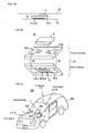
- a metallic body of an automobile serving as the product may be used as the radiation plate
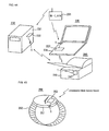
- a metallic case of a mobile terminal device serving as the product may be used as the radiation plate.
- the radiation plate may be a metallic plate which is disposed on the product so as to serve as the radiation plate.
- the power supply circuit may be a lumped-constant resonant circuit including a capacitance element and an inductance element.
- the lumped-constant resonant circuit may be an LC series resonant circuit or an LC parallel resonant circuit.
- the lumped-constant resonant circuit may include a plurality of LC series resonant circuits or a plurality of LC parallel resonant circuits.
- the resonant circuit may include a distributed constant resonant circuit, and in this case, an inductor included in the resonant circuit is formed of a strip line.
- the lumped-constant resonant circuit including a capacitance element and an inductance element is employed, a reduced size is attained and the resonant circuit is prevented from being influenced by other elements such as the radiation plate. If a plurality of resonant circuits are employed and are connected to one another, wideband signals are attained.
- the power supply circuit board may be a multilayer board including a plurality of dielectric layers or magnetic layers laminated to one another, and in this case, the capacitance element and the inductance element are arranged on a surface of the multilayer board or inside the multilayer board.
- the elements (such as electrodes) included in the resonant circuit may be arranged on the surface of the board or inside the board. Accordingly, miniaturization of the board is attained. Furthermore, a degree of freedom of arrangement of the elements included in the resonant circuit is enhanced, and capability of the resonant circuit is improved.
- the multilayer board may be a resin multilayer board including a plurality of resin films laminated to one another or a ceramic multilayer board including a plurality of ceramic films laminated to one another.
- the multilayer board may be a thin-film multilayer board generated using a thin-film formation technique.
- the ceramic films are preferably formed of low-temperature sintered ceramic material. Since silver or copper having low resistance is used for resonant circuit member when the ceramic films are formed of low-temperature sintered ceramic material.
- the power supply circuit board may be a dielectric or magnetic single-layer board.
- at least one of the capacitance element and the inductance element is arranged on a surface of the single-layer board.
- the single-layer board may be formed of resin or ceramic.
- the capacitance element may be arranged between flat electrodes arranged front and back surfaces of the single-layer board, and alternatively, may be arranged between electrodes arranged on one surface of the single-layer board.
- the power supply circuit board is preferably a rigid resin board or a rigid ceramic board.
- the board is rigid, a stable frequency of the transmission signal is attained whenever the power supply circuit board is attached to a portion having any shape in the product.
- the wireless communication circuit board is stably mounted on the rigid board.
- the radiation plate is preferably an electrode having a band shape, and a length of the band-shaped electrode is preferably equal to the integral multiple of a half wavelength of the resonant frequency so that a maximum gain is obtained. Note that, since the frequency is substantially determined by the resonant circuit, the length of the radiation plate is not necessarily be equal to the integral multiple of a half wavelength of the resonant frequency. This is a great advantage when compared with a case where the radiation plate is an antenna element having a specific resonant frequency.
- the wireless communication circuit board and the power supply circuit board may be connected through various methods.
- an electrode on a wireless communication circuit board side may be arranged on the wireless communication circuit board serving as a first board
- an electrode on a first board side may be arranged on the power supply circuit board
- the wireless communication circuit board and the electrode on the first board side may be electrically connected to each other.
- solder, conductive resin, or gold bumps may be used for the connection.
- the electrode on the wireless communication circuit board side and the electrode on the first board side may be electrically connected to each other by capacitance coupling or magnetic-field coupling.
- capacitance coupling or the magnetic-field coupling solder or conductive resin is not required for the connection, and an adhesive agent such as resin is used for bonding.
- the electrode on the wireless communication circuit board side and the electrode on the first board side are not required to be arranged on a surface of the wireless communication circuit board and a surface of the power supply circuit board, respectively.
- a resin film may be formed on the surface of the wireless communication circuit board, or the electrode on the first board side may be arranged in an inner layer of the multilayer board.
- an area of the electrode on the first substrate side is preferably larger than an area of the electrode on the wireless communication circuit board side.
- the electrode on the wireless communication circuit board side and the electrode on the first board side are preferably electrodes having coil shapes.
- a spiral electrode or a helical electrode is readily designed as such a coil electrode.
- a mianda electrode may be effectively used for high frequencies.
- the power supply circuit board and the radiation plate serving as a second board may be connected with each other using various methods.
- an electrode on a second board side and the radiation plate 20 may be connected to each other through capacitance coupling or magnetic-field coupling.
- the capacitance coupling or the magnetic-field coupling is employed, solder or conductive resin is not required for the connection, and an adhesive agent such as resin is used for bonding.
- the electrode on the second board side is not required to be arranged on a surface of the power supply circuit board and a surface of the power supply circuit board, respectively.
- the electrode on the second board side may be arranged in an inner layer of the multilayer board.
- the electrode on the second board side is preferably an electrode having a coil shape.
- a spiral electrode or a helical electrode is readily designed as such a coil electrode.
- a mianda electrode may be effectively used for high frequencies. Note that, when the magnetic-field coupling is employed, it is preferable not to prevent change of magnetic flux generated in the electrode on the second board side (coil electrode), and therefore, opening portions is preferably formed on the radiation plate, for example. By this, transmission efficiency of signal energy is improved, and shifts of frequencies generated due to the bonding are reduced.
- frequencies of a transmission signal and a reception signal are determined by a power supply circuit arranged on a power supply circuit board, even when the power supply circuit board is used in combination with any radiation plate of any configuration, frequency characteristics are not changed and stable frequency characteristics are attained. Furthermore, the power supply circuit board is mounted on the wireless communication circuit board with considerably high accuracy. Accordingly, communication among various products (devices) is achieved by utilizing metallic bodies originally included in the products themselves or metallic plates disposed on the products as radiation plates.
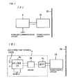
- Fig. 1(A) shows a basic circuit configuration of a product including a power supply circuit board according to the present invention in which a power supply circuit 16 is electrically connected to a wireless communication circuit (modem) 4 and is electromagnetically connected to a radiation plate 20.
- the radiation plate 20 is a metallic body originally included in each of various products which will be described in embodiments below or a metallic plate disposed on each of the various products.
- the wireless communication circuit 4 is mounted on a cellular phone, for example, and includes an RF unit which transmits and receives a high-frequency signal and a BB unit which converts the high-frequency signal into a baseband signal.
- an IC for signal processing and components such as an inductor, a capacitor, and filter are required in order to process a signal using the RF unit and the BB unit.
- the IC and the components are implemented on a predetermined board or are incorporated in a predetermined board whereby the wireless communication circuit 4 is configured. As shown in Fig.
- a Bluetooth communication circuit for example, which is one of near field communication systems includes an RF/BB IC 4a which is an IC for radio communication and for signal processing, a balun 4b which is a balanced-to-unbalanced transformer, and a bandpass filter (BPF) 4c, and is configured as a wireless communication circuit board in which these components are implemented thereon or incorporated therein.
- the power supply circuit 16 includes a resonant circuit having an inductance element, which will be described hereinafter, and is configured as a power supply circuit board.
- the wireless communication circuit 4 has a function of transmitting a signal to and receiving a signal from a reader/writer through the power supply circuit 16.
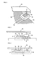
- Fig. 2 shows a first example of a combination of the wireless communication circuit board and the power supply circuit board.
- an electrode arranged on a back surface of a power supply circuit board 10 including the power supply circuit 16 is connected to an electrode 3a arranged on the wireless communication circuit board by soldering, for example, so as to be connected to the wireless communication circuit 4.
- the power supply circuit 16 is connected through electromagnetic-field coupling to the radiation plate 20 through an electrode 25 and a conductor 22 which are arranged on a surface of the power supply circuit board 10.
- a reference numeral 3b denotes a ground electrode. Note that the electrode 25 and the conductor 22 or the radiation plate 20 and the conductor 22 may be electrically connected to each other by soldering or using a dielectric adhesive agent, or may be electrically insulated from each other using an insulation adhesive agent.
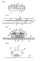
- Fig. 3 shows a second combination example in which the IC 4a, the BPF 4c, and the capacitor 4d are arranged on a board 5 so as to configure the wireless communication circuit 4.
- the balun 4b is incorporated in the board 5.
- the power supply circuit board 10 including the power supply circuit 16 is connected to the board 5 using soldering bumps 6.
- Other configurations are the same as those of the first combination example.
- Fig. 4 shows a third combination example in which the wireless communication circuit 4 and the power supply circuit 16 are integrally arranged on a board 5a.
- the power supply circuit 16 is connected through electromagnetic-field connection to the radiation plate 20 through a conductor 23 which has a spring characteristic and which is pressure-welded on the board 5a.
- Other configurations are the same as those of the second combination example.
- the radiation plate 20 and the conductor 23 may be electrically connected to each other by soldering or using a dielectric adhesive agent, or may be electrically insulated from each other using an insulation adhesive agent.
- Fig. 5 shows a fourth combination example in which the power supply circuit 16 included in the power supply circuit board 10 arranged on the board 5 is connected through electromagnetic-field connection to the radiation plate 20 (metal case) fixedly arranged on the board 5.
- the radiation plate 20 metal case
- An electromagnetic coupling module 1a operates in combination with a monopole radiation plate 20.
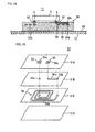
- the electromagnetic coupling module 1a includes a wireless communication circuit board 5 and the power supply circuit board 10 including the circuit board 5 mounted thereon, and is bonded to the radiation plate 20 which is an electrode having a band shape.
- the wireless communication circuit board 5 includes the wireless communication circuit 4 shown in Fig. 1(B) and is electrically connected to the power supply circuit 16 incorporated in the power supply circuit board 10.
- the power supply circuit 16 is used to supply a transmission signal having a predetermined frequency to the radiation plate 20 and/or used to select a reception signal having a predetermined frequency from among signals received using the radiation plate 20 so as to supply the selected signal to the wireless communication circuit board 5.
- the power supply circuit 16 includes a resonant circuit which resonates with the frequencies of the transmission signal and the reception signal.
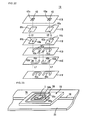
- the power supply circuit board 10 includes the power supply circuit 16 configured as a lumped-constant (LC) series resonant circuit including a helical inductance element L and capacitance elements C1 and C2 as shown in Figs. 7 and 8 . As shown in an exploded perspective view in Fig. 9 in detail, the power supply circuit board 10 includes ceramic sheets 11A to 11G which are laminated and pressure-bonded with one another, and sintered.
- LC lumped-constant
- the sheet 11A includes connection electrodes 12 and via-hole conductors 13a
- the sheet 11B includes capacitor electrodes 14a
- the sheet 11C includes capacitor electrodes 14b and via-hole conductors 13b
- the sheet 11D includes via-hole conductors 13c
- the sheet 11E includes inductor electrodes 15a and via-hole conductors 13d
- the sheet 11F (a single or a plurality of sheets 11F) includes via-hole conductors 13e
- the sheet 11G includes inductor electrodes 15b.
- each of the ceramic sheets 11A to 11G may be formed of a magnetic ceramic member, and the power supply circuit board 10 is more readily obtained by general processing of manufacturing a multilayer substrate, such as a sheet lamination method or a thick-film printing method.
- the inductance element L having an axis of helical winding parallel to the radiation plate 20 is connected to the capacitor electrodes 14b arranged on the opposite sides of the helical inductance element L, and the capacitor electrodes 14a are connected through the via-hole conductors 13a to the connection electrodes 12 whereby the capacitance elements C1 and C2 are formed.
- the connection electrodes 12 serving as electrodes on a wireless communication circuit board side is electrically connected through the soldering bumps 6 to electrodes (not shown) on a power supply circuit board side arranged on the wireless communication circuit board 5.
- the inductance element L which is a coil electrode is used to supply a transmission signal to the radiation plate 20 through magnetic-field coupling, and a reception signal is supplied from the radiation plate 20 to the inductance element L by means of the magnetic-field coupling. Therefore, the power supply circuit board 10 is preferably configured such that, among the inductance elements and the capacitance elements, an inductance element is arranged near the radiation plate 20.
- the radiation plate 20 is a long nonmagnetic body made of an aluminum foil or a copper foil, i.e., a metallic body with both ends open, and is arranged on a product including a flexible insulation resin film 21, such as PET, serving as a base body.
- the back surface of the power supply circuit board 10 is attached by bonding to the radiation plate 20 using an insulating bonding layer such as an adhesive agent 18.
- the wireless communication circuit board 5 has a thickness of 50 to 100 ⁇ m
- the soldering bumps 6 has a thickness of 20 ⁇ m
- the power supply circuit board 10 has a thickness of 200 to 500 ⁇ m
- the adhesive agent 18 has a thickness of 0.1 to 10 ⁇ m
- the radiation plate 20 has a thickness of 1 to 50 ⁇ m
- the resin film 21 has a thickness of 10 to 100 ⁇ m.
- the wireless communication circuit board 5 has a size (area) selected from various sizes such as a size of 0.4 mm ⁇ 0.4 mm and a size of 0.9 mm x 0.8 mm.
- the power supply circuit board 10 is configured so as to have a size (area) in a range from the same as that of the wireless communication circuit board 5 to a size of approximately 3 mm x 3 mm.
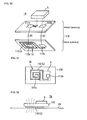
- Figs. 10(A) and 10(B) show states of a connection between the wireless communication circuit board 5 and the power supply circuit board 10.
- a pair of antenna terminals 7a and a pair of antenna terminals 17a are arranged on a back surface of the wireless communication circuit board 5 and the surface of the power supply circuit board 10, respectively.
- Fig. 10(B) which is another connection state, in addition to the pair of antenna terminals 7a and the pair of antenna terminals 17a, ground terminals 7b and ground terminals 17b are arranged on the back surface of the wireless communication circuit board 5 and the surface of the power supply circuit board 10, respectively.
- the ground terminals 17b arranged on the power supply circuit board 10 are terminal ends, and therefore, are not connected to other elements of the power supply circuit board 10.
- Fig. 8 shows an equivalent circuit of the electromagnetic coupling module 1a.
- the electromagnetic coupling module 1a receives using the radiation plate 20 a high-frequency signal (for example, in a UHF frequency band) emitted from a transmitter (not shown), resonates the power supply circuit 16 (the LC series resonant circuit including the inductance element L and the capacitance elements C1 and C2) which is connected to the radiation plate 20 through magnetic-field coupling, and allows only reception signals in a predetermined frequency band to be supplied to the wireless communication circuit 4.
- the power supply circuit 16 rectifies an information signal supplied from the wireless communication circuit 4 so that the signal has a predetermined frequency, and then, supplies a transmission signal from the inductance element L of the power supply circuit 16 to the radiation plate 20 through magnetic-field coupling.
- the signal is output from the radiation plate 20.
- electrostatic-field coupling means connection by means of an electric field and/or magnetic field.
- the wireless communication circuit board 5 is electrically connected to the power supply circuit board 10 which incorporates the power supply circuit 16.
- the power supply circuit board 10 has an area substantially the same as that of the wireless communication circuit board 5 and is rigid. Accordingly, when compared with a case where the wireless communication circuit board 5 is mounted on a flexible film having a large area in the related art, the wireless communication circuit board 5 is accurately positioned and mounted on the power supply circuit board 10. Furthermore, since the power supply circuit board 10 is formed of a ceramic member and has heat resistance, the wireless communication circuit board 5 is mounted on the power supply circuit board 10 by soldering.
- a resonant frequency characteristic is determined by the resonant circuit including the inductance element L and the capacitance elements C1 and C2.
- a resonant frequency of a signal emitted from the radiation plate 20 substantially corresponds to a self-resonant frequency of the power supply circuit 16, and a maximum gain of the signal is substantially determined by at least one of a size of the power supply circuit 16, a shape of the power supply circuit 16, a distance between the power supply circuit 16 and the radiation plate 20, and a medium between the power supply circuit 16 and the radiation plate 20.
- a length of the radiation plate 20 in a longitudinal direction is half a wavelength ⁇ which corresponds to the resonant frequency.
- the length of the radiation plate 20 in the longitudinal direction is not necessarily to be an integral multiple of ⁇ /2. That is, in this embodiment, since the frequency of the signal emitted from the radiation plate 20 is substantially determined by the resonant frequency of the resonant circuit (power supply circuit 16), a frequency characteristic does not substantially depend on the length of the radiation plate 20 in the longitudinal direction. If the length of the radiation plate 20 in the longitudinal direction is an integral multiple of ⁇ /2, the gain becomes maximum, which is preferable.
- the resonant frequency characteristic of the power supply circuit 16 is determined by the resonant circuit including the inductance element L and the capacitance elements C1 and C2 which is incorporated in the power supply circuit board 10, even when the electromagnetic coupling module 1a is inserted into a book, the resonant frequency characteristic does not change. Furthermore, even when the electromagnetic coupling module 1a is rolled so that a shape of the radiation plate 20 is changed or even when the size of the radiation plate 20 is changed, the resonant frequency characteristic does not change.
- the coil electrode constituting the inductance element L has the winding axis parallel to the radiation plate 20, differences between stray capacitances generated between the coil electrode and the radiation plate 20 are small in portions of the coil, and therefore, a center frequency is not changed. Furthermore, since the capacitance elements C1 and C2 are inserted into a subsequent stage of the wireless communication circuit board 5, surge in low frequencies is reduced by the capacitance elements C1 and C2 and the wireless communication circuit board 5 is protected from the surge.
- the power supply circuit board 10 is a rigid multilayer board
- the wireless communication circuit board 5 is readily mounted on the power supply circuit board 10 by soldering.
- the radiation plate 20 is formed of a flexible metallic film, the radiation plate 20 is readily arranged on a wrapping film or arranged on a surface of a cylindrical body.
- the resonant circuit may serve as a matching circuit which matches an impedance of the wireless communication circuit and the impedance of the radiation plate.
- the power supply circuit board may further include a matching circuit including an inductance element and a capacitance element which is provided separately from the resonant circuit.
- An electromagnetic coupling module 1b of a second example is mounted on a radiation plate 20 which is formed of an aluminum foil having a large area, and the radiation plate 20 is arranged on an insulated plastic film 21 having a large area and a flexibility as shown in Fig. 11 .
- a power supply circuit board 10 having a wireless communication circuit board 5 mounted thereon is bonded to an arbitrary portion of the radiation plate 20.
- a configuration of the electromagnetic coupling module 1b that is, an inner configuration of the power supply circuit board 10 is the same as that of the first example. There is an advantage in that high accuracy is not required for a bonding position of the power supply circuit board 10.
- An electromagnetic coupling module 1c is mounted on a mesh portion of a radiation plate 20 which is formed of an aluminum foil, for example, having a large area as shown in Fig. 12 .
- the mesh may be formed on an entire surface of the radiation plate 20 or may be formed on a portion of the surface of the radiation plate 20.
- a configuration of the electromagnetic coupling module 1c is the same as that of the second example.
- a magnetic flux of a coil electrode is transmitted through opening portions of the mesh, and therefore, change (reduction) of the magnetic flux generated from the power supply circuit board 10 is suppressed, and a large amount of magnetic flux is transmitted through the radiation plate 20. Accordingly, transmission efficiency of signal energy is improved, and shifts of frequencies generated due to the bonding are reduced.
- an adhesive agent 18 is applied through a radiation plate 20 to a portion of a surface of a film 21 which contacts to a power supply circuit board 10 and other portions of the surface (entire surface in this example).
- a first product including the electromagnetic coupling module 1d may be bonded to a second product so that the electromagnetic coupling module 1d is incorporated.
- a configuration of the electromagnetic coupling module 1d that is, an inner configuration of the power supply circuit board 10 is the same as that of the first example. Accordingly, effects of the forth example are basically the same as those of the first example.
- Fifth Example of Electromagnetic Coupling Module (refer to Fig. 14 )
- An electromagnetic coupling module 1e is configured such that, as shown in an equivalent circuit of Fig. 14 , an inductance element L which is constituted by a coil electrode serving as a power supply circuit 16 is incorporated in a power supply circuit board 10.
- a capacitance element C is formed as a stray capacitance (distributed constant capacitance) generated between opposite ends of the coil electrode of the inductance element L.
- an L component of the coil electrode itself and a C component corresponding to the stray capacitance between the opposite ends of the electrode are serving as an LC parallel resonant circuit, that is, constitute the power supply circuit 16.
- the electromagnetic coupling module 1e receives using a radiation plate 20 a high-frequency signal (for example, in a UHF frequency band) emitted from a transmitter (not shown), resonates the power supply circuit 16 (the LC parallel resonant circuit including the inductance element L and the capacitance element C) which is connected to the radiation plate 20 mainly through magnetic-field coupling, and allows only reception signals in a predetermined frequency band to be supplied to a wireless communication circuit 4.
- the power supply circuit 16 rectifies an information signal supplied from the wireless communication circuit 4 so that the signal has a predetermined frequency, and then, supplies a transmission signal from the inductance element L of the power supply circuit 16 to the radiation plate 20 through magnetic-field coupling.
- the signal is output from the radiation plate 20.
- An electromagnetic coupling module 1f of a sixth example includes a power supply circuit 16 for radiation plates 20 constituting a dipole radiation plate as shown in an equivalent circuit of Fig. 15 , and the power supply circuit 16 incorporates two LC parallel resonant circuits on a power supply circuit board.
- An inductance element L1 and a capacitance element C1 are connected to a first port of a wireless communication circuit board 5 so as to oppose one of the radiation plates 20 whereas an inductance element L2 and a capacitance element C2 are connected to a second port of the wireless communication circuit board 5 so as to oppose the other of the radiation plates 20.
- Each of the inductance element L1 and the capacitance element C1 has open ends. Note that the first port and the second port constitute an I/O of a differential circuit.
- the electromagnetic coupling module 1f receives using the radiation plates 20 high-frequency signals (for example, in a UHF frequency band) emitted from a transmitter (not shown), resonates the power supply circuit 16 (the LC parallel resonant circuit including the inductance element L1 and the capacitance element C1 and the LC parallel resonant circuit including the inductance element L2 and the capacitance element C2) which is connected to the radiation plates 20 mainly through magnetic-field coupling, and allows only reception signals in a predetermined frequency band to be supplied to a wireless communication circuit 4.
- the power supply circuit 16 the LC parallel resonant circuit including the inductance element L1 and the capacitance element C1 and the LC parallel resonant circuit including the inductance element L2 and the capacitance element C2
- the power supply circuit 16 rectifies information signals supplied from the wireless communication circuit 4 so that the signal has a predetermined frequency, and then, supplies transmission signals from the inductance element L1 and the inductance element L2 of the power supply circuit 16 to the radiation plates 20 through magnetic-field coupling. The signals are output from the radiation plates 20. Seventh Example of Electromagnetic Coupling Module (refer to Fig. 16 )
- An electromagnetic coupling module 1g of a seventh example includes a power supply circuit 16 for radiation plates 20 constituting a dipole radiation plate as shown in an equivalent circuit in Fig. 16 , and the power supply circuit 16 incorporates two LC series resonant circuits on a power supply circuit board. Inductance elements L1 and L2 oppose the radiation plates 20, and capacitance elements C1 and C2 are connected to the ground.
- the electromagnetic coupling module 1g receives using the radiation plates 20 high-frequency signals (for example, in a UHF frequency band) emitted from a transmitter (not shown), resonates the power supply circuit 16 (the LC series resonant circuit including the inductance element L1 and the capacitance element C1 and the LC series resonant circuit including the inductance element L2 and the capacitance element C2) which is connected to the radiation plates 20 mainly through magnetic-field coupling, and allows only reception signals in a predetermined frequency band to be supplied to a wireless communication circuit 4.
- the power supply circuit 16 the LC series resonant circuit including the inductance element L1 and the capacitance element C1 and the LC series resonant circuit including the inductance element L2 and the capacitance element C2
- the power supply circuit 16 rectifies information signals supplied from the wireless communication circuit 4 so that the signal has a predetermined frequency, and then, supplies transmission signals from the inductance element L1 and the inductance element L2 of the power supply circuit 16 to the radiation plates 20 through magnetic-field coupling. The signals are output from the radiation plates 20.
- Eighth Example of Electromagnetic Coupling Module (refer to Figs. 17 to 19 )
- An electromagnetic coupling module 1h of an eighth example operates in combination with a monopole radiation plate 20 as shown in Fig. 17 , and an inductance element L and a capacitance element C which are incorporated in a power supply circuit board 10 and which serve as an LC series resonant circuit constitute a power supply circuit 16.
- a coil electrode constituting the inductance element L has a winding axis perpendicular to the radiation plate 20, and a magnetic field is generated parallel to the winding axis and perpendicular to the radiation plate 20. Eddy current is generated on the radiation plate 20 due to the magnetic field, and the eddy current generates another magnetic field to be emitted from the radiation plate 20.
- the power supply circuit board 10 includes ceramic sheets 31A to 31F which are laminated and pressure-bonded with one another, and sintered.
- the sheet 31A includes connection electrodes 32 and via-hole conductors 33a
- the sheet 31B includes a capacitor electrode 34a and a via-hole conductor 33b
- the sheet 31C includes a capacitor electrode 34b, a via-hole conductor 33c and the via-hole conductor 33b
- the sheet 31D (a single or a plurality of sheets 31D) includes an inductor electrode 35a, a via-hole conductor 33d and the via-hole conductor 33b
- the sheet 31E (a single or a plurality of sheets 31E) includes an inductor electrode 35b, a via-hole conductor 33e, and the via-hole conductor 33b
- the sheet 31F includes an inductor electrode 35c.
- the inductance element L having the axis of helical winding perpendicular to the radiation plate 20 and the power supply circuit 16 constituted by the LC series resonant circuit including the inductance element L and the capacitance element C connected to each other in series are obtained.
- the capacitor electrode 34a is connected to the connection electrode 32 through one of the via-hole conductors 33a, and further connected to a wireless communication circuit board 5 through a soldering bump 6.
- One end of the inductance element L is connected to the connection electrode 32 through the via-hole conductor 33 and further connected to the wireless communication circuit board 5 through a soldering bump 6.
- the electromagnetic coupling module 1h receives using the radiation plate 20 a high-frequency signal (for example, in a UHF frequency band) emitted from a transmitter (not shown), resonates the power supply circuit 16 (the LC series resonant circuit including the inductance element L and the capacitance element C) which is connected to the radiation plate 20 mainly through magnetic-field coupling, and allows only reception signals in a predetermined frequency band to be supplied to a wireless communication circuit 4.
- a high-frequency signal for example, in a UHF frequency band
- the power supply circuit 16 the LC series resonant circuit including the inductance element L and the capacitance element C
- the power supply circuit 16 rectifies an information signal supplied from the wireless communication circuit 4 so that the signal has a predetermined frequency, and then, supplies a transmission signal from the inductance element L of the power supply circuit 16 to the radiation plate 20 through magnetic-field coupling. The signal is output from the radiation plate 20.
- An electromagnetic coupling module 1i of a ninth example is configured, as shown in Fig. 20 , such that a winding width (coil diameter) of the coil electrode of the inductance element L described in the eighth example is gradually increased toward a radiation plate 20.
- Other configurations are the same as those of the eighth example.
- An electromagnetic coupling module 1j of a 10th example operates with radiation plates 20 constituting a dipole radiation plate as shown in an equivalent circuit of Fig. 21 , and has a power supply circuit board 10 incorporating a power supply circuit 16 including two LC series resonant circuits.
- the power supply circuit board 10 includes dielectric ceramic sheets 41A to 41F which are laminated and pressure-bonded with one another, and sintered.
- the sheet 41A includes connection electrodes 42 and via-hole conductors 43a
- the sheet 41B includes capacitor electrodes 44a
- the sheet 41C includes capacitor electrodes 44b and via-hole conductors 43b
- the sheet 41D (a single or a plurality of sheets 41D) includes inductor electrodes 45a and via-hole conductors 43c
- the sheet 41E (a single or a plurality of sheets 41E) includes inductor electrodes 45b and via-hole conductors 43d
- the sheet 41F includes inductor electrodes 45c.
- inductance elements L1 and L2 each having the axes of helical winding perpendicular to the radiation plate 20 and the power supply circuit 16 constituted by the two LC series resonant circuits including the inductance elements L1 and L2 and capacitance elements C1 and C2 which are connected to each other, respectively, in series are obtained.
- the capacitor electrode 44a is connected to the connection electrode 42 through the via-hole conductor 43a, and further connected to a wireless communication circuit board 5 through a soldering bump.
- the electromagnetic coupling module 1j receives using the radiation plates 20 high-frequency signals (for example, in a UHF frequency band) emitted from a transmitter (not shown), resonates the power supply circuit 16 (the LC series resonant circuit including the inductance element L1 and the capacitance element C1 and the LC series resonant circuit including the inductance element L2 and the capacitance element C2) which is connected to the radiation plates 20 mainly through magnetic-field coupling, and allows only reception signals in a predetermined frequency band to be supplied to a wireless communication circuit 4.
- the power supply circuit 16 the LC series resonant circuit including the inductance element L1 and the capacitance element C1 and the LC series resonant circuit including the inductance element L2 and the capacitance element C2
- the power supply circuit 16 rectifies information signals supplied from the wireless communication circuit 4 so that the signal has a predetermined frequency, and then, supplies transmission signals from the inductance element L1 and the inductance element L2 of the power supply circuit 16 to the radiation plates 20 through magnetic-field coupling. The signals are output from the radiation plates 20.
- the capacitance elements C1 and C2 are inserted into a subsequent stage of the wireless communication circuit board 5 and are arranged between the wireless communication circuit board 5 and the inductance elements L1 and L2, surge-resistance property is improved. Since surge is low frequency current up to 200 MHz, the surge is cut using the capacitance elements C1 and C2, and the wireless communication circuit board 5 is prevented from being destroyed by surge.
- the resonant circuit including the capacitance element C1 and the inductance element L1 is not connected to the resonant circuit including the capacitance element C2 and the inductance element L2.
- An electromagnetic coupling module 1k of an 11th example is configured, as shown in Fig. 23 , such that a coil electrode is arranged on a surface of a rigid power supply circuit board 50 formed of ceramic or heat resistant resin, that is, a power supply circuit 56 constituted by a spiral inductance element is arranged on the single-layer board 50. Both ends of the power supply circuit 56 is directly connected to the wireless communication circuit board 5 through soldering bumps, and the power supply circuit board 50 is bonded to a film 21 which supports a radiation plate 20 using an adhesive agent. Furthermore, an inductor electrode 56a intersects with inductor electrodes 56b and 56c and is separated from the inductor electrodes 56b and 56c using an insulating film, not shown.
- the power supply circuit 56 of the 11th example constitutes an LC parallel resonant circuit utilizing a stray capacitance generated in the spiral inductor electrode as a capacitance component.
- the power supply circuit board 50 is the single layer board formed of a dielectric body or a magnetic body.
- the power supply circuit 56 is connected to the radiation plate 20 mainly through magnetic-field coupling. Accordingly, as with the foregoing examples, the electromagnetic coupling module 1k receives using the radiation plate 20 a high-frequency signal emitted from a transmitter, resonates the power supply circuit 56, and allows only reception signals in a predetermined frequency band to be supplied to a wireless communication circuit 4.
- the power supply circuit 56 rectifies an information signal supplied from the wireless communication circuit 4 so that the signal has a predetermined frequency, and then, supplies a transmission signal from the inductance element of the power supply circuit 56 to the radiation plate 20 through magnetic-field coupling. The signal is output from the radiation plate 20.
- the wireless communication circuit board 5 is mounted on the rigid power supply circuit board 50 having a small area, as with the first example, excellent positioning accuracy is attained, and the wireless communication circuit board 5 can be connected to the power supply circuit board 50 using a soldering bump.
- An electromagnetic coupling module 11 of a 12th example is configured such that a coil electrode of a power supply circuit 56 is incorporated in a power supply circuit board 50 as shown in Fig. 24 .
- the power supply circuit board 50 includes dielectric ceramic sheets 51A to 51D which are laminated and pressure-bonded with one another, and sintered.
- the sheet 51A includes connection electrodes 52 and via-hole conductors 53a
- the sheet 51B includes an inductor electrode 54a and via-hole conductors 53b and 53c
- the sheet 51C includes an inductor electrode 54b
- the sheet 51D (a plurality of sheets 51) is a plain sheet.
- the power supply circuit board 50 which incorporates the power supply circuit 56 including a resonant circuit constituted by a spiral inductance element and a capacitance component generated as a stray capacitance in the spiral electrode is obtained.
- Connection electrodes 52 arranged on both ends of the power supply circuit 56 are connected to a wireless communication circuit board 5 through soldering bumps 6. Effects of the 12th example are the same as those of the 11th example.
- An electromagnetic coupling module 1m of a 13th example is configured, as shown in an equivalent circuit of Fig. 26 , such that a power supply circuit board 10 and radiation plates 20 are capacitively-coupled with each other.
- the power supply circuit board 10 includes a power supply circuit 16 having two LC series resonant circuits.
- One end of an inductance element L1 and one end of an inductance element L2 are connected to a wireless communication circuit board 5, and the other end of the inductance element L1 and the other end of the inductance element L2 are connected to capacitor electrodes 72a and 72b (refer to Fig. 27 ), respectively, which are included in capacitance elements C1 and C2, respectively, which are arranged on the power supply circuit board 10.
- capacitor electrodes 72a and 72b respectively, which are included in capacitance elements C1 and C2, respectively, which are arranged on the power supply circuit board 10.
- one end of one of the radiation plates 20 and one end of the other of the radiation plates 20 serve as capacitor electrodes included in the
- the power supply circuit board 10 includes dielectric ceramic sheets 71A to 71F which are laminated and pressure-bonded with one another, and sintered.
- the sheet 71A includes capacitor electrodes 72a and 72b and via-hole conductors 73a and 73b
- each of the sheet 71B to 71E includes inductor electrodes 74a and 74b and via-hole conductors 73c and 73d
- the sheet 71F includes the inductor electrodes 74a and 74b on one side thereof and includes connection electrodes 75a and 75b on the other side thereof which are connected to the inductor electrodes 74a and 74b through via-hole conductors 73e and 73f.
- the power supply circuit 16 including two LC series resonant circuits, one of which includes the inductance element L1 and the capacitance element C1 connected to each other in series and the other of which includes the inductance element L2 and the capacitance element C2 connected to each other in series is obtained. Since the power supply circuit board 10 is bonded to the radiation plate 20 using an adhesive agent, the capacitor electrodes 72a and 72b which are flat electrodes arranged parallel to the radiation plate 20 oppose the ends 20a and the 20b of the radiation plates 20 through an insulation adhesive layer whereby the capacitance elements C1 and C2 are formed.
- connection electrodes 75a and 75b are connected to the wireless communication circuit board 5 through soldering bumps, the one end of the inductance element L1 and the one end of the inductance element L2 are connected to the wireless communication circuit board 5, and the wireless communication circuit board 5 and the power supply circuit board 10 are electrically connected to each other.
- the adhesive agent includes dielectric powder, for example, an adhesive layer has a property of a dielectric body, and accordingly, capacities of the capacitance elements C1 and C2 become large.
- the capacitor electrodes 72a and 72b which serve as electrodes on a second substrate side are arranged on a back surface of the power supply circuit board 10 in the 13th example, the capacitor electrodes 72a and 72b may be arranged inside the power supply circuit board 10 (in particular, near the radiation plate 20). The capacitor electrode 72a and 72b may be arranged in an inner layer of the power supply circuit board 10.
- the electromagnetic coupling module 1m receives using the radiation plates 20 high-frequency signals (for example, in a UHF frequency band) emitted from a transmitter (not shown), resonates the power supply circuit 16 (the LC series resonant circuit including the inductance element L1 and the capacitance element C1 and the LC series resonant circuit including the inductance element L2 and the capacitance element C2) which is connected to the radiation plates 20 mainly in an magnetic-field coupling manner, and allows only reception signals in a predetermined frequency band to be supplied to a wireless communication circuit 4.
- the power supply circuit 16 the LC series resonant circuit including the inductance element L1 and the capacitance element C1 and the LC series resonant circuit including the inductance element L2 and the capacitance element C2
- the power supply circuit 16 rectifies information signals supplied from the wireless communication circuit 4 so that the signal has a predetermined frequency, and then, supplies transmission signals to the radiation plates 20 using the capacitance coupling of the capacitance elements C1 and C2. The signals are output from the radiation plates 20.
- Fourteenth Example of Electromagnetic Coupling Module (refer to Figs. 28 to 30 )
- An electromagnetic coupling module In of a 14th example is configured, as shown in an equivalent circuit of Fig. 28 , such that a power supply circuit 16 includes inductance elements L1 and L2 which are connected to each other through magnetic-field coupling, the inductance element L1 is connected to a wireless communication circuit board 5 through capacitance elements C1a and C1b and connected to the inductance element L2 in parallel through capacitance elements C2a and C2b.
- the power supply circuit 16 includes an LC series resonant circuit having the inductance element L1 and the capacitance elements C1a and C1b and an LC series resonant circuit having the inductance element L2 and the capacitance elements C2a and C2b.
- the resonant circuits are connected to each other through magnetic-field coupling represented by a mutual inductance M as shown in Fig. 28 .
- the inductance elements L1 and L2 are connected to a radiation plate 20 through magnetic-field coupling.
- the power supply circuit board 10 includes dielectric ceramic sheets 81A to 81H which are laminated and pressure-bonded with one another, and sintered.
- the sheet 81A is a plain sheet
- the sheet 81B includes inductor electrodes 82a and 82b and via-hole conductors 83a, 83b, 84a, and 84b
- the sheet 81C includes the inductor electrodes 82a and 82b and via-hole conductors 83c, 84c, 83e, and 84e
- the sheet 81D includes the inductor electrodes 82a and 82b and via-hole conductors 83d, 84d, 83e, and 84e
- the sheet 81E includes capacitor electrodes 85a and 85b and a via-hole conductor 83e
- the sheet 81F includes the capacitor electrodes 86a and 86b
- the sheet 81G is a plain sheet
- the sheet 81H includes capacitor electrodes 87a and 87b
- the inductor electrode 82a is formed as the inductance element L1 through connection using the via-hole conductors 83b and 83c
- the inductor electrode 82b is formed as the inductance element L2 through connection using the via-hole conductors 84b and 84c.
- the capacitor electrodes 86a and 87a constitute a capacitance element C1a, and the capacitor electrode 86a is connected through the via-hole conductor 83e to one end of the inductance element L1.
- the capacitor electrodes 86b and 87b constitute a capacitance element C1b, and the capacitor electrode 86b is connected through the via-hole conductor 83d to the other end of the inductance element L1.
- the capacitor electrodes 85a and 86a constitute a capacitance element C2a, and the capacitor electrode 85a is connected through the via-hole 84e to one end of the inductance element L2.
- the capacitor electrodes 85b and 86b constitute a capacitance element C2b, and the capacitor electrode 85b is connected through the via-hole conductor 84d to the other end of the inductance element L2.
- the electromagnetic coupling module In receives using the radiation plate 20 a high-frequency signal (for example, in a UHF frequency band) emitted from a transmitter (not shown), resonates the power supply circuit 16 (the LC series resonant circuit including the inductance element L1 and the capacitance elements C1a and C1b and the LC series resonant circuit including the inductance element L2 and the capacitance elements C2a and C2b) which is connected to the radiation plate 20 mainly through magnetic-field coupling, and allows only reception signals in a predetermined frequency band to be supplied to a wireless communication circuit 4.
- a high-frequency signal for example, in a UHF frequency band
- the power supply circuit 16 the LC series resonant circuit including the inductance element L1 and the capacitance elements C1a and C1b and the LC series resonant circuit including the inductance element L2 and the capacitance elements C2a and C2b
- the power supply circuit 16 rectifies information signals supplied from the wireless communication circuit 4 so that the signal has a predetermined frequency, and then, supplies transmission signals from the inductance element L1 and L2 of the power supply circuit 16 to the radiation plate 20 through magnetic-field coupling. The signals are output from the radiation plate 20.
- a frequency band is widened as represented by a band width X in Fig. 30 relative to a reflection characteristic.
- the power supply circuit 16 is constituted by the plurality of LC resonant circuits including the inductance elements L1 and L2 which are connected to each other through magnetic-field coupling with a high coupling degree.
- the capacitance elements C1a and C1b are inserted into a subsequent stage of the wireless communication circuit board 5, a surge-resistance property is improved.
- An electromagnetic coupling module 1o of a 15th example is configured, as shown in an equivalent circuit of Fig. 31 , such that a power supply circuit 16 includes inductance elements L1 and L2 which are connected to each other through magnetic-field coupling with a high coupling degree.
- the inductance element L1 is connected to an inductance element L5 arranged on a wireless communication circuit board 5 through magnetic-field coupling, and the inductance element L2 and a capacitance element C2 constitute an LC series resonant circuit.
- the capacitance element C1 is capacitively-coupled with a radiation plate 20, and another capacitance element C3 is inserted between the capacitance elements C1 and C2.
- a power supply circuit board 10 includes dielectric ceramic sheets 91A to 91E which are laminated and pressure-bonded with one another, and sintered.
- the sheet 91A includes inductor electrodes 92a and 92b and via-hole conductors 93a, 93b, 94a, and 94b
- the sheet 91B includes a capacitor electrode 95 and via-hole conductors 93c, 93d, and 94c
- the sheet 91C includes a capacitor electrode 96 and the via-hole conductors 93c and 93d
- the sheet 91D includes a capacitor electrode 97 and the via-hole conductor 93c
- the sheet 91E includes a capacitor electrode 98.
- the inductor electrode 92a constitutes the inductance element L1
- the inductor electrode 92b constitutes the inductance element L2.
- the capacitor electrodes 97 and 98 constitute the capacitance element C1.
- One end of the inductance element L1 is connected through the via-hole conductors 93a and 93c to the capacitor electrode 98, and the other end thereof is connected through the via-hole conductors 93b and 93d to the capacitor electrode 97.
- the capacitor electrodes 95 and 96 constitute the capacitance element C2.
- One end of the inductance element L2 is connected through the via-hole conductors 94a and 94c to the capacitor electrode 96, and the other end thereof is connected through the via-hole conductor 94b to the capacitor electrode 95.
- the capacitor electrodes 96 and 97 constitute the capacitance element C3.
- a coil electrode 99 serving as an electrode on the wireless communication circuit board side is arranged on a back surface of the wireless communication circuit board 5, and serves as the inductance element L5.
- a protection film made of resin for example, is arranged on a surface of the coil electrode 99.
- the electromagnetic coupling module 1o receives using the radiation plate 20 a high-frequency signal (for example, in a UHF frequency band) emitted from a transmitter (not shown), resonates the power supply circuit 16 (the LC series resonant circuit including the inductance element L2 and the capacitance elements C2) which is connected to the radiation plate 20 mainly through magnetic-field coupling, and allows only reception signals in a predetermined frequency band to be supplied to a wireless communication circuit 4.
- the power supply circuit 16 rectifies information signals supplied from the wireless communication circuit 4 so that the signal has a predetermined frequency, and then, supplies transmission signals to the radiation plate 20 through capacitance coupling and magnetic-field coupling.
- the signals are output from the radiation plate 20.
- the power supply circuit 16 and the wireless communication circuit board 5 are connected to each other using the inductance elements L1 and L5 through magnetic-field coupling so that electric power and transmission/reception signals are supplied.
- An electromagnetic coupling module 1p is configured, as shown in an equivalent circuit of Fig. 34 , such that a power supply circuit 16 includes inductance element L1, L2, and L3 which are connected to one another through magnetic-field coupling with a high coupling degree.
- the inductance element L1 is connected to an inductance element L5 arranged on a wireless communication circuit board 5 through magnetic-field coupling
- the inductance element L2 and capacitor electrodes C1a and C1b constitute an LC series resonant circuit
- the inductance element L3 and capacitor electrodes C2a and C2b constitute an LC series resonant circuit.
- the inductance elements L1, L2, and L3 are connected to a radiation plate 20 through magnetic-field coupling.
- a power supply circuit board 10 includes dielectric ceramic sheets 101A to 101E which are laminated and pressure-bonded with one another, and sintered.
- the sheet 101A includes an inductor electrode 102a and via-hole conductors 103a and 103b
- the sheet 101B includes capacitor electrodes 104a and 104b
- the sheet 101C includes capacitor electrodes 105a and 105b and via-hole conductors 103c and 103d
- the sheet 101D includes capacitor electrodes 106a and 106b, the via-hole conductors 103c and 103d, and via-hole conductors 103e and 103f
- the sheet 101E includes inductor electrodes 102b and 102c.
- gaps are generated between the electrodes 104a, 105a, and 106a constituting the capacitor electrodes C1a and C2a and the electrodes 104b, 105b, and 106b constituting the capacitor electrodes C1b and C2b so that a magnetic flux generated by the inductance element L1 reaches the inductance elements L2 and L3 and further reaches the radiation plate 20.
- the inductor electrode 102a constitutes the inductance element L1
- the inductor electrode 102b constitutes the inductance element L2
- the inductor electrode 102c constitutes the inductance element L3.
- the capacitor electrodes 104a and 105a constitute the capacitance element C1a
- the capacitor electrodes 104b and 105b constitute the capacitance element C1b
- the capacitor electrodes 105a and 106a constitute the capacitance element C2a
- the capacitor electrodes 105b and 106b constitute the capacitance element C2b.
- One end of the inductance element L1 is connected through the via-hole conductor 103a to the capacitor electrode 104a, and the other end thereof is connected through the via-hole conductor 103b to the to capacitor electrode 104b.
- One end of the inductance element L2 is connected through the via-hole conductor 103c to the capacitor electrode 105a, and the other end thereof is connected through the via-hole conductor 103f to the capacitor electrode 106b.
- One end of the inductance element L3 is connected through the via-hole conductor 103e to the capacitor electrode 106a, and the other end thereof is connected through the via-hole conductor 103d to the capacitor electrode 105b.
- a coil electrode 99 serving as an electrode on the wireless communication circuit board side is arranged on a back surface of the wireless communication circuit board 5, and serves as the inductance element L5.
- a protection film made of resin for example, is arranged on a surface of the coil electrode 99.
- the electromagnetic coupling module 1p receives using the radiation plate 20 a high-frequency signal (for example, in a UHF frequency band) emitted from a transmitter (not shown), resonates the power supply circuit 16 (the LC series resonant circuit including the inductance element L2 and the capacitance elements C1a and C1b and the LC series resonant circuit including the inductance element L3 and the capacitance elements C2a and C2b) which is connected to the radiation plate 20 mainly through magnetic-field coupling, and allows only reception signals in a predetermined frequency band to be supplied to a wireless communication circuit 4.
- a high-frequency signal for example, in a UHF frequency band
- the power supply circuit 16 the LC series resonant circuit including the inductance element L2 and the capacitance elements C1a and C1b and the LC series resonant circuit including the inductance element L3 and the capacitance elements C2a and C2b
- the power supply circuit 16 rectifies information signals supplied from the wireless communication circuit 4 so that the signal has a predetermined frequency, and then, supplies transmission signals from the inductance elements L1, L2, and L3 to the radiation plate 20 through magnetic-field coupling. The signals are output from the radiation plate 20.
- the power supply circuit 16 and the wireless communication circuit board 5 are connected to each other using the inductance elements L1 and L5 through magnetic-field coupling so that electric power and transmission/reception signals are transmitted.
- the power supply circuit 16 is constituted by the plurality of LC resonant circuits including the inductance elements L2 and L3 which are connected to each other through magnetic-field coupling in the 16th example.
- An electromagnetic coupling module 1q of a 17th example includes a power supply circuit board 110 which is a single-layer board, and an equivalent circuit thereof is the same as that shown in Fig. 8 .
- the power supply circuit 16 is configured such that capacitance elements C1 and C2 are connected to both ends of an inductance element L whereby an LC series resonant circuit is constituted.
- the power supply circuit board 110 is dielectric ceramic board, and has capacitor electrodes 111a and 111b on a surface thereof and capacitor electrodes 112a and 112b and an inductor electrode 113 on a back surface thereof as shown in Fig. 36 .
- the capacitor electrodes 111a and 112a constitute the capacitance element C1
- the capacitor electrodes 111b and 112b constitute the capacitance element C2.
- the electromagnetic coupling module 1q receives using the radiation plate 20 a high-frequency signal (for example, in a UHF frequency band) emitted from a transmitter (not shown), resonates the power supply circuit 16 (the LC series resonant circuit including the inductance element L and the capacitance elements C1 and C2) which is connected to the radiation plate 20 mainly through magnetic-field coupling, and allows only reception signals in a predetermined frequency band to be supplied to a wireless communication circuit 4.
- a high-frequency signal for example, in a UHF frequency band
- the power supply circuit 16 the LC series resonant circuit including the inductance element L and the capacitance elements C1 and C2
- the power supply circuit 16 rectifies an information signal supplied from the wireless communication circuit 4 so that the signal has a predetermined frequency, and then, supplies a transmission signal from the inductance element L of the power supply circuit 16 to the radiation plate 20 through magnetic-field coupling.
- the signals are output from the radiation plate 20.
- the inductance element L is arranged so as to only partially overlap with the wireless communication circuit board 5 in a plan view as shown in Figs. 37 and 38 . Therefore, most magnetic flux generated in the inductance element L is not prevented from transmitted by the wireless communication circuit board 5, and initial rise of the magnetic flux is improved.
- the power supply circuit board 110 on which the wireless communication circuit board 5 is arranged may be sandwiched between radiation plates 20 as shown in Fig. 39 .
- Efficiency of magnetic-field coupling between the power supply circuit 16 and the radiation plates 20 is improved and gain is improved.
- An electromagnetic coupling module 1r of an 18th example is configured such that an inductance element L is formed by a mianda line electrode, and an equivalent circuit thereof is the same as that shown in Fig. 8 .
- a power supply circuit 16 is configured such that capacitance elements C1 and C2 are connected to both ends of an inductance element L whereby an LC series resonant circuit is constituted.
- the power supply circuit board 110 is dielectric ceramic single-layer board, and has capacitor electrodes 121a and 121b on a surface thereof and capacitor electrodes 122a and 122b and a mianda inductor electrode 123 on a back surface thereof as shown in Fig. 40 .
- the capacitor electrodes 121a and 122a constitute the capacitance element C1 and the capacitor electrodes 121b and 122b constitute the capacitance element C2.
- the electromagnetic coupling module 1r receives using the radiation plate 20 a high-frequency signal (for example, in a UHF frequency band) emitted from a transmitter (not shown), resonates the power supply circuit 16 (the LC series resonant circuit including the inductance element L and the capacitance elements C1 and C2) which is connected to the radiation plate 20 mainly through magnetic-field coupling, and allows only reception signals in a predetermined frequency band to be supplied to a wireless communication circuit 4.
- a high-frequency signal for example, in a UHF frequency band
- the power supply circuit 16 the LC series resonant circuit including the inductance element L and the capacitance elements C1 and C2
- the power supply circuit 16 rectifies an information signal supplied from the wireless communication circuit 4 so that the signal has a predetermined frequency, and then, supplies a transmission signal from the inductance element L of the power supply circuit 16 to the radiation plate through magnetic-field coupling. The signals are output from the radiation plate.
- the inductance element L is constituted by the mianda inductor electrode 123, transmission and reception of a high-frequency signal are effectively performed.
- the power supply circuit board 110 may be constituted by a multilayer board.
- a first embodiment is applied to an automobile 200, and a car body 201 of the automobile 200, which is made of a steel plate, is used as a radiation plate.
- the automobile 200 includes an ETC transmitter/receiver 205, a navigation device 206 including a television set, and a car radio 207.
- an electromagnetic coupling module 1 which includes a wireless communication circuit board (modem) incorporating reception circuits (and a transmission circuits as needed) which receive signals for the respective devices (such as an ETC signal, a GPS signal, a television signal, and a radio signal) is attached to the steel plate portion of the car body 201, and the power supply circuit is connected to the steel plate portion (radiation plate) through electromagnetic-field coupling.
- the reception circuits (and the transmission circuits as needed) for the respective devices are electrically connected to the wireless communication circuit board.
- the first embodiment is applicable not only to the automobile 200 but also to vehicles such as trains, airplanes, ships, buses, construction equipment such as mobile cranes, forklift trucks, motorcycles, and bicycles.
- a second embodiment is applied to illuminating lamps 210 which are installed in expressways, and metallic pole portions 211 of the illuminating lamps 210 are used as radiation plates.
- electromagnetic coupling modules 1 power supply circuits are electromagnetically connected to the pole portions 211, and each of the electromagnetic coupling modules 1 receives a control signal (such as a light-on signal and a light-off signal) transmitted from a controller 215.
- the control signal is supplied through wireless communication circuit boards (modems) to illumination control units 212 so that light-on operations or light-off operations are performed.
- the illumination control units 212 may be incorporated in the corresponding wireless communication circuit boards.
- the illuminating lamps 210 include Zigbee (registered trademark) systems. Specifically, when one of the illuminating lamps 210 which is located nearest to the controller 215 is controlled, the control signal is successively transferred to other illuminating lamps 210 located near the one of the illuminating lamps 210 so that the illuminating lamps located in distant places are successively controlled.
- Zigbee registered trademark
- a third embodiment is applied to an electronic paper 220 including a display screen 221 and a frame portion 222, and the metallic frame portion 222 of the electronic paper 220 is used as a radiation plate.
- a power supply circuit in an electromagnetic coupling module 1 is electromagnetically connected to the frame portion 222, and receives a control signal and a display image signal transmitted from a display signal transmitter 225.
- the control signal and the display image signal are supplied through a wireless communication board (modem) to a reception circuit 223 and a display circuit 224. Accordingly, an image is displayed in the display screen 221 or is replaced by a new one.
- the reception circuit 223 may be incorporated in the wireless communication circuit board.
- a metallic case portion 231 of a body 230 of a desktop personal computer and a metallic case portion 236 of a laptop personal computer 235 are used as radiation plates.
- Power supply circuits of electromagnetic coupling modules 1 are electromagnetically connected to the case portions 231 and 236, and are connected through wireless communication circuit boards (modems) to transmission/reception circuits 232 and 237.
- the electromagnetic coupling module 1 receives a signal supplied from a wireless LAN (W-LAN) 241 and transmits a signal to the W-LAN 241.
- WLAN wireless LAN
- a case portion 246 of a printer 245 may be used as the radiation plate.
- a wireless communication circuit board (modem) connected to a transmission/reception circuit 247 communicates with the wireless communication circuit boards included in the body 230 and the laptop personal computer 235.
- a metallic case 251 and a band 252 of an atomic clock 250 are used as a radiation plate.
- a power supply circuit of an electromagnetic coupling module 1 is electromagnetically connected to the case 251 and the band 252 so that a standard time electric wave is supplied.
- a wireless communication circuit board (modem) is connected to a time correction circuit 253. Note that the time correction circuit 253 may be incorporated in the wireless communication circuit board.
- a metallic case portion 261 (dielectric coating which is applied to the case when the case portion is a nonmetallic case portion) of a cellular phone 260 is used as a radiation plate.
- a electromagnetic coupling module 1 supports a plurality of frequencies, and a power supply circuit is electromagnetically connected to the case portion 261 and the dielectric coating so as to receive c a digital terrestrial signal, a GPS signal, a WiFi signal, and a calling signal such as a CDMA or a GSM.
- a wireless communication circuit board (modem) is connected to reception circuits provided for the respective signals.
- the sixth embodiment is applicable not only the cellular phone 260 but also mobile devices such as a PDA, a digital still camera, a mobile game device, and a communication device.
- mobile devices such as a PDA, a digital still camera, a mobile game device, and a communication device.
- a metallic case portion 321 of a television set 320 and a metallic case portion 326 of a DVD recorder 325 are used as radiation plates.
- Power supply circuits of electromagnetic coupling modules 1 are electromagnetically connected to the respective case portions 321 and 326, and wireless communication circuit boards (modems) of the electromagnetic coupling modules 1 are connected to respective transmission/reception circuits 322 and 327.
- the wireless communication circuit boards communicate with each other through UWB communication.
- a metallic case portion 331 of a television set 330 and a metallic case portion 336 of a radio 335 are used as radiation plates.
- Electromagnetic coupling modules 1 support a plurality of frequencies, and power supply circuits are electromagnetically connected to the respective case portions 331 and 336 or dielectric coating so as to receive a terrestrial television signal and a radio signal.
- Wireless communication circuit boards are connected to reception circuits 332 and 337 provided for the respective signals.
- a metallic case portion 341 of a refrigerator 340 is used as a radiation plate.
- a power supply circuit of an electromagnetic coupling module 1 is electromagnetically connected to a case portion 341 and a wireless communication circuit board (modem) of the electromagnetic coupling module 1 is connected to a transmission/reception circuit 342.
- the wireless communication circuit board is wirelessly communicated with a home controller (not shown) based on the Echonet standard so as to manage foods stored in a refrigerator 340. If electromagnetic coupling modules 1 are attached to the foods stored in the refrigerator 340, use-by dates are easily managed. Since the refrigerator 340 is normally in a turn-on state, the refrigerator 340 is appropriately used as a home server.
- free electrons filled in a fluorescent light tube 400 is used as radiation plates.
- a power supply circuit is electromagnetically connected to the free electrons in the tube by attaching an electromagnetic coupling module 1 to a surface of the fluorescent light tube 400.
- a wireless communication circuit board (modem) is connected to the Internet through a transmission/reception circuit 401, a PLC 402, and a rooter 403.
- a personal computer 405 communicates with the Internet through the electromagnetic coupling module 1 using a WiFi signal and a UWB signal.
- the wireless communication circuit board may store therein location information of the fluorescent light tube 400 in an indoor place and may transmit the location information to a mobile terminal or a reader/writer device so as to inform a visually impaired person who has the mobile terminal or the reader/writer device of location.
- the product to which the power supply circuit board is attached is not limited to the products described in the foregoing embodiment, and the power supply circuit board may be attached to various products.
- detailed internal configuration of the power supply circuit board and a detailed shape of the radiation plate may be arbitrarily set, and the board may be a rigid board or a flexible board.
- the wireless communication circuit board may be connected to the power supply circuit board not only by a soldering bump but also in other ways.
- the present invention is applicable to product used in RFID systems, and the present invention is excellent in terms of a stable frequency characteristic and capability of communication between various products.
Landscapes
- Engineering & Computer Science (AREA)
- Microelectronics & Electronic Packaging (AREA)
- Computer Hardware Design (AREA)
- Physics & Mathematics (AREA)
- General Physics & Mathematics (AREA)
- Theoretical Computer Science (AREA)
- Computer Networks & Wireless Communication (AREA)
- Near-Field Transmission Systems (AREA)
- Details Of Aerials (AREA)
- Supply And Installment Of Electrical Components (AREA)
- Support Of Aerials (AREA)
Abstract
Description
- The present invention relates to products including power supply circuit boards, and particularly, relates to a product which includes a power supply circuit board having a power supply circuit electrically connected to a wireless communication circuit and which is used in an RFID (Radio Frequency Identification) system.
- In general, as a product management system, an RFID system in which a reader/writer which generates an induction field and an IC tag (hereinafter referred to as a "wireless IC device") which stores therein predetermined information regarding a product are communicated with each other in a noncontact manner so that the information is transmitted has been developed. Examples of the wireless IC device used in the RFID system include devices disclosed in
Patent Documents - Specifically, a device including a
plastic film 600, anantenna pattern 601 arranged on theplastic film 600, and awireless IC chip 610 arranged on one end of theantenna pattern 601 as shown inFig. 51 , and a device including aplastic film 620, anantenna pattern 621 arranged on theplastic film 620, radiatingelectrodes 622 arranged on theplastic film 620, and awireless IC chip 610 arranged on a predetermined portion of theantenna pattern 621 as shown inFig. 52 have been proposed. - However, since in the wireless IC devices in the related art, the
wireless IC chip 610 is arranged on each of theantenna patterns antenna patterns wireless IC chip 610 should be positioned on each of thefilms wireless IC chip 610 on each of thefilms antenna pattern antenna pattern - Although possibilities of use of such a wireless IC device are infinite, it is still difficult to arrange the wireless IC device on various products since resonant frequency characteristics are changed in accordance with an arrangement state of an antenna.
- Patent Document 1: Japanese Unexamined Patent Application Publication No.
2005-136528 - Patent Document 2: Japanese Unexamined Patent Application Publication No.
2005-244778 - Accordingly, an object of the present invention is to provide a product including a power supply circuit board which has a power supply circuit having stable frequency characteristics and which enables communication among various types of product (device).
- To attain the object, a product including a power supply circuit board according to the present invention, the power supply circuit board including a power supply circuit mounted thereon having an inductance element, includes a wireless communication circuit board which is electrically connected to the power supply circuit, wherein one of the power supply circuit board and the wireless communication circuit board is mounted on the other or the power supply circuit board and the wireless communication circuit board are integrally formed as a board, and the other board or the integrally-formed board is mounted on the product, and the product includes a radiation plate having at least one of two functions, i.e., a function of emitting a transmission signal which is supplied from the power supply circuit through electromagnetic-field coupling and which has a frequency substantially determined in accordance with a resonant frequency of the power supply circuit, and a function of supplying a reception signal to the power supply circuit through the electromagnetic-field coupling.
- In the product including the power supply circuit board according to the present invention, the wireless communication circuit board is electrically connected to the power supply circuit board, and since the power supply circuit board is disposed on the product, the power supply circuit board and the radiation plate are connected to each other through electromagnetic-field connection. The frequency of the transmission signal emitted from the radiation plate and a frequency of a reception signal to be supplied to the wireless communication circuit board are substantially determined in accordance with the resonant circuit of the power supply circuit in the power supply circuit board. Here, these frequencies are "substantially" determined since the frequencies slightly shift due to the positional relationship between the power supply circuit board and the radiation plate. That is, since the frequency of the transmission signal and the reception signal are determined by the power supply circuit board connected to the wireless communication circuit board, frequency characteristics are not changed due to a shape, a size and an arrangement position of the radiation plate, that is, frequency characteristics are not changed even when the radiation plate is rolled or is sandwiched between dielectric bodies. Accordingly, stable frequency characteristics are attained. Consequently, communication among various products (devices) is achieved.
- In the product including the power supply circuit board according to the present invention, the radiation plate may be a metallic member originally included in the product. For example, a metallic body of an automobile serving as the product may be used as the radiation plate, and a metallic case of a mobile terminal device serving as the product may be used as the radiation plate. Furthermore, the radiation plate may be a metallic plate which is disposed on the product so as to serve as the radiation plate.
- In the product including the power supply circuit board according to the present invention, the power supply circuit may be a lumped-constant resonant circuit including a capacitance element and an inductance element. The lumped-constant resonant circuit may be an LC series resonant circuit or an LC parallel resonant circuit. Alternatively, the lumped-constant resonant circuit may include a plurality of LC series resonant circuits or a plurality of LC parallel resonant circuits. The resonant circuit may include a distributed constant resonant circuit, and in this case, an inductor included in the resonant circuit is formed of a strip line. However, if the lumped-constant resonant circuit including a capacitance element and an inductance element is employed, a reduced size is attained and the resonant circuit is prevented from being influenced by other elements such as the radiation plate. If a plurality of resonant circuits are employed and are connected to one another, wideband signals are attained.
- When the capacitance element is arranged between the wireless communication circuit board and the inductance element, surge-resistance property is improved. Since surge is low frequency current up to 200 MHz, the surge is cut using the capacitance element, and the wireless communication circuit board is prevented from being destroyed by the surge.
- The power supply circuit board may be a multilayer board including a plurality of dielectric layers or magnetic layers laminated to one another, and in this case, the capacitance element and the inductance element are arranged on a surface of the multilayer board or inside the multilayer board. When the power supply circuit board corresponds to the multilayer board, the elements (such as electrodes) included in the resonant circuit may be arranged on the surface of the board or inside the board. Accordingly, miniaturization of the board is attained. Furthermore, a degree of freedom of arrangement of the elements included in the resonant circuit is enhanced, and capability of the resonant circuit is improved. The multilayer board may be a resin multilayer board including a plurality of resin films laminated to one another or a ceramic multilayer board including a plurality of ceramic films laminated to one another. Alternatively, the multilayer board may be a thin-film multilayer board generated using a thin-film formation technique. When the ceramic multilayer board is employed, the ceramic films are preferably formed of low-temperature sintered ceramic material. Since silver or copper having low resistance is used for resonant circuit member when the ceramic films are formed of low-temperature sintered ceramic material.
- The power supply circuit board may be a dielectric or magnetic single-layer board. In this case, at least one of the capacitance element and the inductance element is arranged on a surface of the single-layer board. The single-layer board may be formed of resin or ceramic. The capacitance element may be arranged between flat electrodes arranged front and back surfaces of the single-layer board, and alternatively, may be arranged between electrodes arranged on one surface of the single-layer board.
- The power supply circuit board is preferably a rigid resin board or a rigid ceramic board. In this case, since the board is rigid, a stable frequency of the transmission signal is attained whenever the power supply circuit board is attached to a portion having any shape in the product. In addition, the wireless communication circuit board is stably mounted on the rigid board.
- The radiation plate is preferably an electrode having a band shape, and a length of the band-shaped electrode is preferably equal to the integral multiple of a half wavelength of the resonant frequency so that a maximum gain is obtained. Note that, since the frequency is substantially determined by the resonant circuit, the length of the radiation plate is not necessarily be equal to the integral multiple of a half wavelength of the resonant frequency. This is a great advantage when compared with a case where the radiation plate is an antenna element having a specific resonant frequency.
- Furthermore, the wireless communication circuit board and the power supply circuit board may be connected through various methods. For example, an electrode on a wireless communication circuit board side may be arranged on the wireless communication circuit board serving as a first board, an electrode on a first board side may be arranged on the power supply circuit board, and the wireless communication circuit board and the electrode on the first board side may be electrically connected to each other. In this case, solder, conductive resin, or gold bumps may be used for the connection.
- Alternatively, the electrode on the wireless communication circuit board side and the electrode on the first board side may be electrically connected to each other by capacitance coupling or magnetic-field coupling. When the capacitance coupling or the magnetic-field coupling is employed, solder or conductive resin is not required for the connection, and an adhesive agent such as resin is used for bonding. In this case, the electrode on the wireless communication circuit board side and the electrode on the first board side are not required to be arranged on a surface of the wireless communication circuit board and a surface of the power supply circuit board, respectively. For example, a resin film may be formed on the surface of the wireless communication circuit board, or the electrode on the first board side may be arranged in an inner layer of the multilayer board.
- When the capacitance coupling is employed, an area of the electrode on the first substrate side is preferably larger than an area of the electrode on the wireless communication circuit board side. By this, even if positional accuracy is deteriorated when the wireless communication circuit board is mounted on the power supply circuit board, variation of a capacitance generated between the electrodes is reduced. Furthermore, although it is difficult to arrange an electrode having a large area on the small wireless communication circuit board, the electrode having a large area is readily arranged on the comparatively large power supply circuit board.
- When the magnetic-field coupling is employed, when compared with the capacitance coupling, considerably high mounting accuracy of the wireless communication circuit board onto the power supply circuit board is not required, and accordingly, mounting thereof is further facilitated. Moreover, the electrode on the wireless communication circuit board side and the electrode on the first board side are preferably electrodes having coil shapes. A spiral electrode or a helical electrode is readily designed as such a coil electrode. A mianda electrode may be effectively used for high frequencies.
- In addition, the power supply circuit board and the radiation plate serving as a second board may be connected with each other using various methods. For example, an electrode on a second board side and the
radiation plate 20 may be connected to each other through capacitance coupling or magnetic-field coupling. When the capacitance coupling or the magnetic-field coupling is employed, solder or conductive resin is not required for the connection, and an adhesive agent such as resin is used for bonding. In this case, the electrode on the second board side is not required to be arranged on a surface of the power supply circuit board and a surface of the power supply circuit board, respectively. For example, the electrode on the second board side may be arranged in an inner layer of the multilayer board. - When the magnetic-field coupling is employed, the electrode on the second board side is preferably an electrode having a coil shape. A spiral electrode or a helical electrode is readily designed as such a coil electrode. A mianda electrode may be effectively used for high frequencies. Note that, when the magnetic-field coupling is employed, it is preferable not to prevent change of magnetic flux generated in the electrode on the second board side (coil electrode), and therefore, opening portions is preferably formed on the radiation plate, for example. By this, transmission efficiency of signal energy is improved, and shifts of frequencies generated due to the bonding are reduced.
- According to the present invention, since frequencies of a transmission signal and a reception signal are determined by a power supply circuit arranged on a power supply circuit board, even when the power supply circuit board is used in combination with any radiation plate of any configuration, frequency characteristics are not changed and stable frequency characteristics are attained. Furthermore, the power supply circuit board is mounted on the wireless communication circuit board with considerably high accuracy. Accordingly, communication among various products (devices) is achieved by utilizing metallic bodies originally included in the products themselves or metallic plates disposed on the products as radiation plates.
-
-
Figs. 1(A) and 1(B) are block diagrams illustrating basic configurations of a power supply circuit and a wireless communication circuit which are included in a product according to the present invention. -
Fig. 2 is a perspective view illustrating a first example of a combination of a wireless communication circuit board and a power supply circuit board. -
Fig. 3 is a side view illustrating a second example of the combination of the wireless communication circuit board and the power supply circuit board. -
Fig. 4 is a side view illustrating a third example of the combination of the wireless communication circuit board and the power supply circuit board. -
Fig. 5 is a sectional view illustrating a fourth example of the combination of the wireless communication circuit board and the power supply circuit board. -
Fig. 6 is a perspective view illustrating a first example of an electromagnetic coupling module. -
Fig. 7 is a sectional view illustrating the first example. -
Fig. 8 is a diagram illustrating an equivalent circuit of the first example. -
Fig. 9 is an exploded perspective view illustrating the power supply circuit board of the first example. -
Figs. 10(A) and 10(B) are perspective views illustrating states of a connection between the wireless communication circuit board and the power supply circuit board. -
Fig. 11 is a perspective view illustrating a second example of the electromagnetic coupling module. -
Fig. 12 is a perspective view illustrating a third example of the electromagnetic coupling module. -
Fig. 13 is a sectional view illustrating a fourth example of the electromagnetic coupling module. -
Fig. 14 is an equivalent circuit diagram illustrating a fifth example of the electromagnetic coupling module. -
Fig. 15 is an equivalent circuit diagram illustrating a sixth example of the electromagnetic coupling module. -
Fig. 16 is an equivalent circuit diagram illustrating a seventh example of the electromagnetic coupling module. -
Fig. 17 is a sectional view illustrating an eighth example of the electromagnetic coupling module. -
Fig. 18 is a diagram illustrating an equivalent circuit of the eighth example. -
Fig. 19 is an exploded perspective view illustrating a power supply circuit board of the eighth example. -
Fig. 20 is an equivalent circuit diagram illustrating a ninth example of the electromagnetic coupling module. -
Fig. 21 is an equivalent circuit diagram illustrating a 10th example of the electromagnetic coupling module. -
Fig. 22 is an exploded perspective view illustrating a power supply circuit board of the 10th example. -
Fig. 23 is a perspective view illustrating an 11th example of the electromagnetic coupling module. -
Fig. 24 is a sectional view illustrating a 12th example of the electromagnetic coupling module. -
Fig. 25 is an exploded perspective view illustrating a power supply circuit board of the 12th example. -
Fig. 26 is a diagram illustrating an equivalent circuit of the 13th example. -
Fig. 27 is an exploded perspective view illustrating a power supply circuit board of the 13th example. -
Fig. 28 is a sectional view illustrating a 14th example of the electromagnetic coupling module. -
Fig. 29 is an exploded perspective view illustrating a power supply circuit board of the 14th example. -
Fig. 30 is a graph illustrating a reflection characteristic of the 14th example. -
Fig. 31 is a sectional view illustrating a 15th example of the electromagnetic coupling module. -
Fig. 32 is an exploded perspective view illustrating a power supply circuit board of the 15th example. -
Fig. 33 shows diagrams illustrating wireless communication circuit board of the 15th example, whereinFig. 33(A) is a bottom view andFig. 33(B) is an enlarged sectional view. -
Fig. 34 is a sectional view illustrating a 16th example of the electromagnetic coupling module. -
Fig. 35 is an exploded perspective view illustrating a power supply circuit board of the 16th example. -
Fig. 36 is an exploded perspective view illustrating a 17th example of the electromagnetic coupling module. -
Fig. 37 is a bottom view of a power supply circuit board including a wireless communication circuit board mounted thereon of the 17th example. -
Fig. 38 is a side view illustrating the 17th example. -
Fig. 39 is a side view illustrating a modification of the 17th example. -
Fig. 40 is an exploded perspective view illustrating an 18th example of the electromagnetic coupling module. -
Fig. 41 is a perspective view illustrating a product including a power supply circuit board according to a first embodiment of the present invention. -
Fig. 42 is a perspective view illustrating a product including a power supply circuit board according to a second embodiment of the present invention. -
Fig. 43 is a front view illustrating a product including a power supply circuit board according to a third embodiment of the present invention. -
Fig. 44 is a perspective view illustrating a product including a power supply circuit board according to a fourth embodiment of the present invention. -
Fig. 45 is a perspective view illustrating a product including a power supply circuit board according to a fifth embodiment of the present invention. -
Fig. 46 is a perspective view illustrating a product including a power supply circuit board according to a sixth embodiment of the present invention. -
Fig. 47 is a perspective view illustrating a product including a power supply circuit board according to a seventh embodiment of the present invention. -
Fig. 48 is a perspective view illustrating a product including a power supply circuit board according to an eighth embodiment of the present invention. -
Fig. 49 is a perspective view illustrating a product including a power supply circuit board according to a ninth embodiment of the present invention. -
Fig. 50 is a perspective view illustrating a product including a power supply circuit board according to a 10th embodiment of the present invention. -
Fig. 51 is a plan view illustrating a first example of a wireless IC device in the related art. -
Fig. 52 is a plan view illustrating a second example of the wireless IC device in the related art. - Embodiments of a product including a power supply circuit board according to the present invention will be described hereinafter with reference to the accompanying drawings. Note that components used in various wireless communication circuit boards, various power supply circuit boards, and various products in common are denoted by identical reference numerals, and therefore, redundant descriptions thereof are omitted.
-
Fig. 1(A) shows a basic circuit configuration of a product including a power supply circuit board according to the present invention in which apower supply circuit 16 is electrically connected to a wireless communication circuit (modem) 4 and is electromagnetically connected to aradiation plate 20. Theradiation plate 20 is a metallic body originally included in each of various products which will be described in embodiments below or a metallic plate disposed on each of the various products. - The
wireless communication circuit 4 is mounted on a cellular phone, for example, and includes an RF unit which transmits and receives a high-frequency signal and a BB unit which converts the high-frequency signal into a baseband signal. Note that an IC for signal processing and components such as an inductor, a capacitor, and filter are required in order to process a signal using the RF unit and the BB unit. The IC and the components are implemented on a predetermined board or are incorporated in a predetermined board whereby thewireless communication circuit 4 is configured. As shown inFig. 1(B) , a Bluetooth communication circuit, for example, which is one of near field communication systems includes an RF/BB IC 4a which is an IC for radio communication and for signal processing, abalun 4b which is a balanced-to-unbalanced transformer, and a bandpass filter (BPF) 4c, and is configured as a wireless communication circuit board in which these components are implemented thereon or incorporated therein. Thepower supply circuit 16 includes a resonant circuit having an inductance element, which will be described hereinafter, and is configured as a power supply circuit board. Furthermore, thewireless communication circuit 4 has a function of transmitting a signal to and receiving a signal from a reader/writer through thepower supply circuit 16. Combination of Wireless Communication Circuit Board and Power Supply Circuit Board (refer toFigs. 2 to 5 ) -
Fig. 2 shows a first example of a combination of the wireless communication circuit board and the power supply circuit board. InFig. 2 , an electrode arranged on a back surface of a powersupply circuit board 10 including thepower supply circuit 16 is connected to an electrode 3a arranged on the wireless communication circuit board by soldering, for example, so as to be connected to thewireless communication circuit 4. Thepower supply circuit 16 is connected through electromagnetic-field coupling to theradiation plate 20 through anelectrode 25 and aconductor 22 which are arranged on a surface of the powersupply circuit board 10. Areference numeral 3b denotes a ground electrode. Note that theelectrode 25 and theconductor 22 or theradiation plate 20 and theconductor 22 may be electrically connected to each other by soldering or using a dielectric adhesive agent, or may be electrically insulated from each other using an insulation adhesive agent. -
Fig. 3 shows a second combination example in which theIC 4a, theBPF 4c, and thecapacitor 4d are arranged on aboard 5 so as to configure thewireless communication circuit 4. Thebalun 4b is incorporated in theboard 5. Furthermore, the powersupply circuit board 10 including thepower supply circuit 16 is connected to theboard 5 using soldering bumps 6. Other configurations are the same as those of the first combination example. -
Fig. 4 shows a third combination example in which thewireless communication circuit 4 and thepower supply circuit 16 are integrally arranged on aboard 5a. Thepower supply circuit 16 is connected through electromagnetic-field connection to theradiation plate 20 through aconductor 23 which has a spring characteristic and which is pressure-welded on theboard 5a. Other configurations are the same as those of the second combination example. Note that, as with the first combination example, theradiation plate 20 and theconductor 23 may be electrically connected to each other by soldering or using a dielectric adhesive agent, or may be electrically insulated from each other using an insulation adhesive agent. -
Fig. 5 shows a fourth combination example in which thepower supply circuit 16 included in the powersupply circuit board 10 arranged on theboard 5 is connected through electromagnetic-field connection to the radiation plate 20 (metal case) fixedly arranged on theboard 5. Other configurations are the same as those of the second combination example. - An
electromagnetic coupling module 1a according to a first example operates in combination with amonopole radiation plate 20. As shown inFigs. 6 and 7 , theelectromagnetic coupling module 1a includes a wirelesscommunication circuit board 5 and the powersupply circuit board 10 including thecircuit board 5 mounted thereon, and is bonded to theradiation plate 20 which is an electrode having a band shape. The wirelesscommunication circuit board 5 includes thewireless communication circuit 4 shown inFig. 1(B) and is electrically connected to thepower supply circuit 16 incorporated in the powersupply circuit board 10. - The
power supply circuit 16 is used to supply a transmission signal having a predetermined frequency to theradiation plate 20 and/or used to select a reception signal having a predetermined frequency from among signals received using theradiation plate 20 so as to supply the selected signal to the wirelesscommunication circuit board 5. Thepower supply circuit 16 includes a resonant circuit which resonates with the frequencies of the transmission signal and the reception signal. - The power
supply circuit board 10 includes thepower supply circuit 16 configured as a lumped-constant (LC) series resonant circuit including a helical inductance element L and capacitance elements C1 and C2 as shown inFigs. 7 and 8 . As shown in an exploded perspective view inFig. 9 in detail, the powersupply circuit board 10 includesceramic sheets 11A to 11G which are laminated and pressure-bonded with one another, and sintered. Thesheet 11A includesconnection electrodes 12 and via-hole conductors 13a, thesheet 11B includes capacitor electrodes 14a, thesheet 11C includescapacitor electrodes 14b and via-hole conductors 13b, thesheet 11D includes via-hole conductors 13c, thesheet 11E includesinductor electrodes 15a and via-hole conductors 13d, thesheet 11F (a single or a plurality ofsheets 11F) includes via-hole conductors 13e, and thesheet 11G includesinductor electrodes 15b. Note that each of theceramic sheets 11A to 11G may be formed of a magnetic ceramic member, and the powersupply circuit board 10 is more readily obtained by general processing of manufacturing a multilayer substrate, such as a sheet lamination method or a thick-film printing method. - By laminating the
sheets 11A to 11G, the inductance element L having an axis of helical winding parallel to theradiation plate 20 is connected to thecapacitor electrodes 14b arranged on the opposite sides of the helical inductance element L, and the capacitor electrodes 14a are connected through the via-hole conductors 13a to theconnection electrodes 12 whereby the capacitance elements C1 and C2 are formed. Then, theconnection electrodes 12 serving as electrodes on a wireless communication circuit board side is electrically connected through the soldering bumps 6 to electrodes (not shown) on a power supply circuit board side arranged on the wirelesscommunication circuit board 5. - That is, among the elements included in the power supply circuit, the inductance element L which is a coil electrode is used to supply a transmission signal to the
radiation plate 20 through magnetic-field coupling, and a reception signal is supplied from theradiation plate 20 to the inductance element L by means of the magnetic-field coupling. Therefore, the powersupply circuit board 10 is preferably configured such that, among the inductance elements and the capacitance elements, an inductance element is arranged near theradiation plate 20. - In the first example, the
radiation plate 20 is a long nonmagnetic body made of an aluminum foil or a copper foil, i.e., a metallic body with both ends open, and is arranged on a product including a flexibleinsulation resin film 21, such as PET, serving as a base body. The back surface of the powersupply circuit board 10 is attached by bonding to theradiation plate 20 using an insulating bonding layer such as anadhesive agent 18. - In terms of sizes, for example, the wireless
communication circuit board 5 has a thickness of 50 to 100 µm, the soldering bumps 6 has a thickness of 20 µm, the powersupply circuit board 10 has a thickness of 200 to 500 µm, theadhesive agent 18 has a thickness of 0.1 to 10 µm, theradiation plate 20 has a thickness of 1 to 50 µm, and theresin film 21 has a thickness of 10 to 100 µm. Furthermore, the wirelesscommunication circuit board 5 has a size (area) selected from various sizes such as a size of 0.4 mm × 0.4 mm and a size of 0.9 mm x 0.8 mm. The powersupply circuit board 10 is configured so as to have a size (area) in a range from the same as that of the wirelesscommunication circuit board 5 to a size of approximately 3 mm x 3 mm. -
Figs. 10(A) and 10(B) show states of a connection between the wirelesscommunication circuit board 5 and the powersupply circuit board 10. InFig. 10(A) , a pair ofantenna terminals 7a and a pair ofantenna terminals 17a are arranged on a back surface of the wirelesscommunication circuit board 5 and the surface of the powersupply circuit board 10, respectively. InFig. 10(B) which is another connection state, in addition to the pair ofantenna terminals 7a and the pair ofantenna terminals 17a,ground terminals 7b andground terminals 17b are arranged on the back surface of the wirelesscommunication circuit board 5 and the surface of the powersupply circuit board 10, respectively. Note that theground terminals 17b arranged on the powersupply circuit board 10 are terminal ends, and therefore, are not connected to other elements of the powersupply circuit board 10. -
Fig. 8 shows an equivalent circuit of theelectromagnetic coupling module 1a. Theelectromagnetic coupling module 1a receives using theradiation plate 20 a high-frequency signal (for example, in a UHF frequency band) emitted from a transmitter (not shown), resonates the power supply circuit 16 (the LC series resonant circuit including the inductance element L and the capacitance elements C1 and C2) which is connected to theradiation plate 20 through magnetic-field coupling, and allows only reception signals in a predetermined frequency band to be supplied to thewireless communication circuit 4. Thepower supply circuit 16 rectifies an information signal supplied from thewireless communication circuit 4 so that the signal has a predetermined frequency, and then, supplies a transmission signal from the inductance element L of thepower supply circuit 16 to theradiation plate 20 through magnetic-field coupling. The signal is output from theradiation plate 20. - Note that although the
power supply circuit 16 and theradiation plate 20 are connected to each other mainly through magnetic-field coupling, electric-field coupling may be employed. In the present invention, the term "electromagnetic-field coupling" means connection by means of an electric field and/or magnetic field. - In the
electromagnetic coupling module 1a of the first example, the wirelesscommunication circuit board 5 is electrically connected to the powersupply circuit board 10 which incorporates thepower supply circuit 16. The powersupply circuit board 10 has an area substantially the same as that of the wirelesscommunication circuit board 5 and is rigid. Accordingly, when compared with a case where the wirelesscommunication circuit board 5 is mounted on a flexible film having a large area in the related art, the wirelesscommunication circuit board 5 is accurately positioned and mounted on the powersupply circuit board 10. Furthermore, since the powersupply circuit board 10 is formed of a ceramic member and has heat resistance, the wirelesscommunication circuit board 5 is mounted on the powersupply circuit board 10 by soldering. That is, unlike the related art, since an ultrasonic bonding method is not used, cost is reduced, deterioration of the wirelesscommunication circuit board 5 due to pressure applied at a time of ultrasonic bonding is avoided, and a self-alignment operation by the reflow soldering may be utilized. - Furthermore, in the
power supply circuit 16, a resonant frequency characteristic is determined by the resonant circuit including the inductance element L and the capacitance elements C1 and C2. A resonant frequency of a signal emitted from theradiation plate 20 substantially corresponds to a self-resonant frequency of thepower supply circuit 16, and a maximum gain of the signal is substantially determined by at least one of a size of thepower supply circuit 16, a shape of thepower supply circuit 16, a distance between thepower supply circuit 16 and theradiation plate 20, and a medium between thepower supply circuit 16 and theradiation plate 20. Specifically, in the first example, a length of theradiation plate 20 in a longitudinal direction is half a wavelength λ which corresponds to the resonant frequency. However, the length of theradiation plate 20 in the longitudinal direction is not necessarily to be an integral multiple of λ/2. That is, in this embodiment, since the frequency of the signal emitted from theradiation plate 20 is substantially determined by the resonant frequency of the resonant circuit (power supply circuit 16), a frequency characteristic does not substantially depend on the length of theradiation plate 20 in the longitudinal direction. If the length of theradiation plate 20 in the longitudinal direction is an integral multiple of λ/2, the gain becomes maximum, which is preferable. - As described above, since the resonant frequency characteristic of the
power supply circuit 16 is determined by the resonant circuit including the inductance element L and the capacitance elements C1 and C2 which is incorporated in the powersupply circuit board 10, even when theelectromagnetic coupling module 1a is inserted into a book, the resonant frequency characteristic does not change. Furthermore, even when theelectromagnetic coupling module 1a is rolled so that a shape of theradiation plate 20 is changed or even when the size of theradiation plate 20 is changed, the resonant frequency characteristic does not change. Moreover, since the coil electrode constituting the inductance element L has the winding axis parallel to theradiation plate 20, differences between stray capacitances generated between the coil electrode and theradiation plate 20 are small in portions of the coil, and therefore, a center frequency is not changed. Furthermore, since the capacitance elements C1 and C2 are inserted into a subsequent stage of the wirelesscommunication circuit board 5, surge in low frequencies is reduced by the capacitance elements C1 and C2 and the wirelesscommunication circuit board 5 is protected from the surge. - Furthermore, since the power
supply circuit board 10 is a rigid multilayer board, the wirelesscommunication circuit board 5 is readily mounted on the powersupply circuit board 10 by soldering. Moreover, since theradiation plate 20 is formed of a flexible metallic film, theradiation plate 20 is readily arranged on a wrapping film or arranged on a surface of a cylindrical body. - Note that, in this embodiment, the resonant circuit may serve as a matching circuit which matches an impedance of the wireless communication circuit and the impedance of the radiation plate. Alternatively, the power supply circuit board may further include a matching circuit including an inductance element and a capacitance element which is provided separately from the resonant circuit. When a function of the matching circuit is added to the resonant circuit, design of the resonant circuit is likely to be complicated. However, when the matching circuit is provided separately from the resonant circuit, each of the resonant circuit and the matching circuit is independently designed. Second Example of Electromagnetic Coupling Module (refer to
Fig. 11 ) - An
electromagnetic coupling module 1b of a second example is mounted on aradiation plate 20 which is formed of an aluminum foil having a large area, and theradiation plate 20 is arranged on aninsulated plastic film 21 having a large area and a flexibility as shown inFig. 11 . A powersupply circuit board 10 having a wirelesscommunication circuit board 5 mounted thereon is bonded to an arbitrary portion of theradiation plate 20. - Note that a configuration of the
electromagnetic coupling module 1b, that is, an inner configuration of the powersupply circuit board 10 is the same as that of the first example. There is an advantage in that high accuracy is not required for a bonding position of the powersupply circuit board 10. - An electromagnetic coupling module 1c is mounted on a mesh portion of a
radiation plate 20 which is formed of an aluminum foil, for example, having a large area as shown inFig. 12 . The mesh may be formed on an entire surface of theradiation plate 20 or may be formed on a portion of the surface of theradiation plate 20. - A configuration of the electromagnetic coupling module 1c is the same as that of the second example. In addition to the advantage in which high accuracy is not required for a bonding position of a power
supply circuit board 10, a magnetic flux of a coil electrode is transmitted through opening portions of the mesh, and therefore, change (reduction) of the magnetic flux generated from the powersupply circuit board 10 is suppressed, and a large amount of magnetic flux is transmitted through theradiation plate 20. Accordingly, transmission efficiency of signal energy is improved, and shifts of frequencies generated due to the bonding are reduced. - According to an
electromagnetic coupling module 1d of a forth example, as shown inFig. 13 , anadhesive agent 18 is applied through aradiation plate 20 to a portion of a surface of afilm 21 which contacts to a powersupply circuit board 10 and other portions of the surface (entire surface in this example). A first product including theelectromagnetic coupling module 1d may be bonded to a second product so that theelectromagnetic coupling module 1d is incorporated. - Note that a configuration of the
electromagnetic coupling module 1d, that is, an inner configuration of the powersupply circuit board 10 is the same as that of the first example. Accordingly, effects of the forth example are basically the same as those of the first example. Fifth Example of Electromagnetic Coupling Module (refer toFig. 14 ) - An
electromagnetic coupling module 1e is configured such that, as shown in an equivalent circuit ofFig. 14 , an inductance element L which is constituted by a coil electrode serving as apower supply circuit 16 is incorporated in a powersupply circuit board 10. A capacitance element C is formed as a stray capacitance (distributed constant capacitance) generated between opposite ends of the coil electrode of the inductance element L. - That is, even when a single coil electrode is provided, if the coil electrode has a self resonance, an L component of the coil electrode itself and a C component corresponding to the stray capacitance between the opposite ends of the electrode are serving as an LC parallel resonant circuit, that is, constitute the
power supply circuit 16. Accordingly, theelectromagnetic coupling module 1e receives using aradiation plate 20 a high-frequency signal (for example, in a UHF frequency band) emitted from a transmitter (not shown), resonates the power supply circuit 16 (the LC parallel resonant circuit including the inductance element L and the capacitance element C) which is connected to theradiation plate 20 mainly through magnetic-field coupling, and allows only reception signals in a predetermined frequency band to be supplied to awireless communication circuit 4. Thepower supply circuit 16 rectifies an information signal supplied from thewireless communication circuit 4 so that the signal has a predetermined frequency, and then, supplies a transmission signal from the inductance element L of thepower supply circuit 16 to theradiation plate 20 through magnetic-field coupling. The signal is output from theradiation plate 20. - An electromagnetic coupling module 1f of a sixth example includes a
power supply circuit 16 forradiation plates 20 constituting a dipole radiation plate as shown in an equivalent circuit ofFig. 15 , and thepower supply circuit 16 incorporates two LC parallel resonant circuits on a power supply circuit board. An inductance element L1 and a capacitance element C1 are connected to a first port of a wirelesscommunication circuit board 5 so as to oppose one of theradiation plates 20 whereas an inductance element L2 and a capacitance element C2 are connected to a second port of the wirelesscommunication circuit board 5 so as to oppose the other of theradiation plates 20. Each of the inductance element L1 and the capacitance element C1 has open ends. Note that the first port and the second port constitute an I/O of a differential circuit. - Effects of the sixth example are basically the same as those of the first example. Specifically, the electromagnetic coupling module 1f receives using the
radiation plates 20 high-frequency signals (for example, in a UHF frequency band) emitted from a transmitter (not shown), resonates the power supply circuit 16 (the LC parallel resonant circuit including the inductance element L1 and the capacitance element C1 and the LC parallel resonant circuit including the inductance element L2 and the capacitance element C2) which is connected to theradiation plates 20 mainly through magnetic-field coupling, and allows only reception signals in a predetermined frequency band to be supplied to awireless communication circuit 4. Thepower supply circuit 16 rectifies information signals supplied from thewireless communication circuit 4 so that the signal has a predetermined frequency, and then, supplies transmission signals from the inductance element L1 and the inductance element L2 of thepower supply circuit 16 to theradiation plates 20 through magnetic-field coupling. The signals are output from theradiation plates 20. Seventh Example of Electromagnetic Coupling Module (refer toFig. 16 ) - An
electromagnetic coupling module 1g of a seventh example includes apower supply circuit 16 forradiation plates 20 constituting a dipole radiation plate as shown in an equivalent circuit inFig. 16 , and thepower supply circuit 16 incorporates two LC series resonant circuits on a power supply circuit board. Inductance elements L1 and L2 oppose theradiation plates 20, and capacitance elements C1 and C2 are connected to the ground. - Effects of the seventh example are basically the same as those of the first example. Specifically, the
electromagnetic coupling module 1g receives using theradiation plates 20 high-frequency signals (for example, in a UHF frequency band) emitted from a transmitter (not shown), resonates the power supply circuit 16 (the LC series resonant circuit including the inductance element L1 and the capacitance element C1 and the LC series resonant circuit including the inductance element L2 and the capacitance element C2) which is connected to theradiation plates 20 mainly through magnetic-field coupling, and allows only reception signals in a predetermined frequency band to be supplied to awireless communication circuit 4. Thepower supply circuit 16 rectifies information signals supplied from thewireless communication circuit 4 so that the signal has a predetermined frequency, and then, supplies transmission signals from the inductance element L1 and the inductance element L2 of thepower supply circuit 16 to theradiation plates 20 through magnetic-field coupling. The signals are output from theradiation plates 20. Eighth Example of Electromagnetic Coupling Module (refer toFigs. 17 to 19 ) - An
electromagnetic coupling module 1h of an eighth example operates in combination with amonopole radiation plate 20 as shown inFig. 17 , and an inductance element L and a capacitance element C which are incorporated in a powersupply circuit board 10 and which serve as an LC series resonant circuit constitute apower supply circuit 16. As shown inFig. 18 , a coil electrode constituting the inductance element L has a winding axis perpendicular to theradiation plate 20, and a magnetic field is generated parallel to the winding axis and perpendicular to theradiation plate 20. Eddy current is generated on theradiation plate 20 due to the magnetic field, and the eddy current generates another magnetic field to be emitted from theradiation plate 20. - As shown in
Fig. 19 in detail, the powersupply circuit board 10 includesceramic sheets 31A to 31F which are laminated and pressure-bonded with one another, and sintered. Thesheet 31A includesconnection electrodes 32 and via-hole conductors 33a, thesheet 31B includes acapacitor electrode 34a and a via-hole conductor 33b, thesheet 31C includes acapacitor electrode 34b, a via-hole conductor 33c and the via-hole conductor 33b, thesheet 31D (a single or a plurality ofsheets 31D) includes an inductor electrode 35a, a via-hole conductor 33d and the via-hole conductor 33b, thesheet 31E (a single or a plurality ofsheets 31E) includes aninductor electrode 35b, a via-hole conductor 33e, and the via-hole conductor 33b, and thesheet 31F includes aninductor electrode 35c. - By laminating the
sheets 31A to 31F, the inductance element L having the axis of helical winding perpendicular to theradiation plate 20 and thepower supply circuit 16 constituted by the LC series resonant circuit including the inductance element L and the capacitance element C connected to each other in series are obtained. Thecapacitor electrode 34a is connected to theconnection electrode 32 through one of the via-hole conductors 33a, and further connected to a wirelesscommunication circuit board 5 through asoldering bump 6. One end of the inductance element L is connected to theconnection electrode 32 through the via-hole conductor 33 and further connected to the wirelesscommunication circuit board 5 through asoldering bump 6. - Effects of the eighth example are basically the same as those of the first example. Specifically, the
electromagnetic coupling module 1h receives using theradiation plate 20 a high-frequency signal (for example, in a UHF frequency band) emitted from a transmitter (not shown), resonates the power supply circuit 16 (the LC series resonant circuit including the inductance element L and the capacitance element C) which is connected to theradiation plate 20 mainly through magnetic-field coupling, and allows only reception signals in a predetermined frequency band to be supplied to awireless communication circuit 4. Thepower supply circuit 16 rectifies an information signal supplied from thewireless communication circuit 4 so that the signal has a predetermined frequency, and then, supplies a transmission signal from the inductance element L of thepower supply circuit 16 to theradiation plate 20 through magnetic-field coupling. The signal is output from theradiation plate 20. - In particular, in the eighth example, there is an advantage in that since the coil electrode has the winding axis perpendicular to the
radiation plate 20, an amount of magnetic field component to theradiation plate 20 is increased, and accordingly, transmission efficiency of signal energy is improved and large gain is attained. Ninth Example of Electromagnetic Coupling Module (refer toFig. 20 ) - An electromagnetic coupling module 1i of a ninth example is configured, as shown in
Fig. 20 , such that a winding width (coil diameter) of the coil electrode of the inductance element L described in the eighth example is gradually increased toward aradiation plate 20. Other configurations are the same as those of the eighth example. - Effects of the ninth example is the same as those of the eighth example. In addition, since the winding width (coil diameter) of the coil electrode of the inductance element L is gradually increased toward the
radiation plate 20, transmission efficiency of signals is improved. Tenth Example of Electromagnetic Coupling Module (refer toFigs. 21 and22 ) - An
electromagnetic coupling module 1j of a 10th example operates withradiation plates 20 constituting a dipole radiation plate as shown in an equivalent circuit ofFig. 21 , and has a powersupply circuit board 10 incorporating apower supply circuit 16 including two LC series resonant circuits. - As shown in
Fig. 22 in detail, the powersupply circuit board 10 includes dielectricceramic sheets 41A to 41F which are laminated and pressure-bonded with one another, and sintered. Thesheet 41A includesconnection electrodes 42 and via-hole conductors 43a, thesheet 41B includes capacitor electrodes 44a, the sheet 41C includescapacitor electrodes 44b and via-hole conductors 43b, thesheet 41D (a single or a plurality ofsheets 41D) includesinductor electrodes 45a and via-hole conductors 43c, thesheet 41E (a single or a plurality ofsheets 41E) includesinductor electrodes 45b and via-hole conductors 43d, and thesheet 41F includesinductor electrodes 45c. - By laminating the
sheets 41A to 41F, inductance elements L1 and L2 each having the axes of helical winding perpendicular to theradiation plate 20 and thepower supply circuit 16 constituted by the two LC series resonant circuits including the inductance elements L1 and L2 and capacitance elements C1 and C2 which are connected to each other, respectively, in series are obtained. The capacitor electrode 44a is connected to theconnection electrode 42 through the via-hole conductor 43a, and further connected to a wirelesscommunication circuit board 5 through a soldering bump. - Effects of the 10th example are basically the same as those of the first example. Specifically, the
electromagnetic coupling module 1j receives using theradiation plates 20 high-frequency signals (for example, in a UHF frequency band) emitted from a transmitter (not shown), resonates the power supply circuit 16 (the LC series resonant circuit including the inductance element L1 and the capacitance element C1 and the LC series resonant circuit including the inductance element L2 and the capacitance element C2) which is connected to theradiation plates 20 mainly through magnetic-field coupling, and allows only reception signals in a predetermined frequency band to be supplied to awireless communication circuit 4. Thepower supply circuit 16 rectifies information signals supplied from thewireless communication circuit 4 so that the signal has a predetermined frequency, and then, supplies transmission signals from the inductance element L1 and the inductance element L2 of thepower supply circuit 16 to theradiation plates 20 through magnetic-field coupling. The signals are output from theradiation plates 20. - Furthermore, since the capacitance elements C1 and C2 are inserted into a subsequent stage of the wireless
communication circuit board 5 and are arranged between the wirelesscommunication circuit board 5 and the inductance elements L1 and L2, surge-resistance property is improved. Since surge is low frequency current up to 200 MHz, the surge is cut using the capacitance elements C1 and C2, and the wirelesscommunication circuit board 5 is prevented from being destroyed by surge. - Note that, in the 10th example, the resonant circuit including the capacitance element C1 and the inductance element L1 is not connected to the resonant circuit including the capacitance element C2 and the inductance element L2.
- An
electromagnetic coupling module 1k of an 11th example is configured, as shown inFig. 23 , such that a coil electrode is arranged on a surface of a rigid powersupply circuit board 50 formed of ceramic or heat resistant resin, that is, apower supply circuit 56 constituted by a spiral inductance element is arranged on the single-layer board 50. Both ends of thepower supply circuit 56 is directly connected to the wirelesscommunication circuit board 5 through soldering bumps, and the powersupply circuit board 50 is bonded to afilm 21 which supports aradiation plate 20 using an adhesive agent. Furthermore, aninductor electrode 56a intersects withinductor electrodes inductor electrodes - The
power supply circuit 56 of the 11th example constitutes an LC parallel resonant circuit utilizing a stray capacitance generated in the spiral inductor electrode as a capacitance component. The powersupply circuit board 50 is the single layer board formed of a dielectric body or a magnetic body. - In the
electromagnetic coupling module 1k of the 11th example, thepower supply circuit 56 is connected to theradiation plate 20 mainly through magnetic-field coupling. Accordingly, as with the foregoing examples, theelectromagnetic coupling module 1k receives using theradiation plate 20 a high-frequency signal emitted from a transmitter, resonates thepower supply circuit 56, and allows only reception signals in a predetermined frequency band to be supplied to awireless communication circuit 4. Thepower supply circuit 56 rectifies an information signal supplied from thewireless communication circuit 4 so that the signal has a predetermined frequency, and then, supplies a transmission signal from the inductance element of thepower supply circuit 56 to theradiation plate 20 through magnetic-field coupling. The signal is output from theradiation plate 20. - Since the wireless
communication circuit board 5 is mounted on the rigid powersupply circuit board 50 having a small area, as with the first example, excellent positioning accuracy is attained, and the wirelesscommunication circuit board 5 can be connected to the powersupply circuit board 50 using a soldering bump. - An
electromagnetic coupling module 11 of a 12th example is configured such that a coil electrode of apower supply circuit 56 is incorporated in a powersupply circuit board 50 as shown inFig. 24 . As shown inFig. 25 , the powersupply circuit board 50 includes dielectricceramic sheets 51A to 51D which are laminated and pressure-bonded with one another, and sintered. Thesheet 51A includesconnection electrodes 52 and via-hole conductors 53a, thesheet 51B includes aninductor electrode 54a and via-hole conductors sheet 51C includes aninductor electrode 54b, and the sheet 51D (a plurality of sheets 51) is a plain sheet. - By laminating the
sheets 51A to 51D, in the coil electrode, the powersupply circuit board 50 which incorporates thepower supply circuit 56 including a resonant circuit constituted by a spiral inductance element and a capacitance component generated as a stray capacitance in the spiral electrode is obtained.Connection electrodes 52 arranged on both ends of thepower supply circuit 56 are connected to a wirelesscommunication circuit board 5 through soldering bumps 6. Effects of the 12th example are the same as those of the 11th example. - An
electromagnetic coupling module 1m of a 13th example is configured, as shown in an equivalent circuit ofFig. 26 , such that a powersupply circuit board 10 andradiation plates 20 are capacitively-coupled with each other. The powersupply circuit board 10 includes apower supply circuit 16 having two LC series resonant circuits. One end of an inductance element L1 and one end of an inductance element L2 are connected to a wirelesscommunication circuit board 5, and the other end of the inductance element L1 and the other end of the inductance element L2 are connected tocapacitor electrodes Fig. 27 ), respectively, which are included in capacitance elements C1 and C2, respectively, which are arranged on the powersupply circuit board 10. Note that one end of one of theradiation plates 20 and one end of the other of theradiation plates 20 serve as capacitor electrodes included in the capacitance elements C1 and C2, respectively. - As shown in
Fig. 27 in detail, the powersupply circuit board 10 includes dielectricceramic sheets 71A to 71F which are laminated and pressure-bonded with one another, and sintered. Thesheet 71A includescapacitor electrodes hole conductors 73a and 73b, each of thesheet 71B to 71E includesinductor electrodes hole conductors sheet 71F includes theinductor electrodes connection electrodes inductor electrodes hole conductors 73e and 73f. - By laminating the
sheets 71A to 71F, thepower supply circuit 16 including two LC series resonant circuits, one of which includes the inductance element L1 and the capacitance element C1 connected to each other in series and the other of which includes the inductance element L2 and the capacitance element C2 connected to each other in series is obtained. Since the powersupply circuit board 10 is bonded to theradiation plate 20 using an adhesive agent, thecapacitor electrodes radiation plate 20 oppose theends 20a and the 20b of theradiation plates 20 through an insulation adhesive layer whereby the capacitance elements C1 and C2 are formed. In addition, since theconnection electrodes communication circuit board 5 through soldering bumps, the one end of the inductance element L1 and the one end of the inductance element L2 are connected to the wirelesscommunication circuit board 5, and the wirelesscommunication circuit board 5 and the powersupply circuit board 10 are electrically connected to each other. - Note that if the adhesive agent includes dielectric powder, for example, an adhesive layer has a property of a dielectric body, and accordingly, capacities of the capacitance elements C1 and C2 become large. Furthermore, although the
capacitor electrodes supply circuit board 10 in the 13th example, thecapacitor electrodes capacitor electrode supply circuit board 10. - Effects of the 13th example are basically the same as those of the first example. Specifically, the
electromagnetic coupling module 1m receives using theradiation plates 20 high-frequency signals (for example, in a UHF frequency band) emitted from a transmitter (not shown), resonates the power supply circuit 16 (the LC series resonant circuit including the inductance element L1 and the capacitance element C1 and the LC series resonant circuit including the inductance element L2 and the capacitance element C2) which is connected to theradiation plates 20 mainly in an magnetic-field coupling manner, and allows only reception signals in a predetermined frequency band to be supplied to awireless communication circuit 4. Thepower supply circuit 16 rectifies information signals supplied from thewireless communication circuit 4 so that the signal has a predetermined frequency, and then, supplies transmission signals to theradiation plates 20 using the capacitance coupling of the capacitance elements C1 and C2. The signals are output from theradiation plates 20. Fourteenth Example of Electromagnetic Coupling Module (refer toFigs. 28 to 30 ) - An electromagnetic coupling module In of a 14th example is configured, as shown in an equivalent circuit of
Fig. 28 , such that apower supply circuit 16 includes inductance elements L1 and L2 which are connected to each other through magnetic-field coupling, the inductance element L1 is connected to a wirelesscommunication circuit board 5 through capacitance elements C1a and C1b and connected to the inductance element L2 in parallel through capacitance elements C2a and C2b. In other words, thepower supply circuit 16 includes an LC series resonant circuit having the inductance element L1 and the capacitance elements C1a and C1b and an LC series resonant circuit having the inductance element L2 and the capacitance elements C2a and C2b. The resonant circuits are connected to each other through magnetic-field coupling represented by a mutual inductance M as shown inFig. 28 . The inductance elements L1 and L2 are connected to aradiation plate 20 through magnetic-field coupling. - As shown in
Fig. 29 in detail, the powersupply circuit board 10 includes dielectricceramic sheets 81A to 81H which are laminated and pressure-bonded with one another, and sintered. Thesheet 81A is a plain sheet, thesheet 81B includesinductor electrodes hole conductors sheet 81C includes theinductor electrodes hole conductors sheet 81D includes theinductor electrodes hole conductors sheet 81E includescapacitor electrodes 85a and 85b and a via-hole conductor 83e, thesheet 81F includes thecapacitor electrodes 86a and 86b, thesheet 81G is a plain sheet, and thesheet 81H includescapacitor electrodes 87a and 87b on a back surface thereof. - By laminating the
sheets 81A to 81H, theinductor electrode 82a is formed as the inductance element L1 through connection using the via-hole conductors 83b and 83c, and theinductor electrode 82b is formed as the inductance element L2 through connection using the via-hole conductors 84b and 84c. The capacitor electrodes 86a and 87a constitute a capacitance element C1a, and the capacitor electrode 86a is connected through the via-hole conductor 83e to one end of the inductance element L1. Thecapacitor electrodes capacitor electrode 86b is connected through the via-hole conductor 83d to the other end of the inductance element L1. The capacitor electrodes 85a and 86a constitute a capacitance element C2a, and the capacitor electrode 85a is connected through the via-hole 84e to one end of the inductance element L2. Thecapacitor electrodes capacitor electrode 85b is connected through the via-hole conductor 84d to the other end of the inductance element L2. - Effects of the 14th example are basically the same as those of the first example. Specifically, the electromagnetic coupling module In receives using the
radiation plate 20 a high-frequency signal (for example, in a UHF frequency band) emitted from a transmitter (not shown), resonates the power supply circuit 16 (the LC series resonant circuit including the inductance element L1 and the capacitance elements C1a and C1b and the LC series resonant circuit including the inductance element L2 and the capacitance elements C2a and C2b) which is connected to theradiation plate 20 mainly through magnetic-field coupling, and allows only reception signals in a predetermined frequency band to be supplied to awireless communication circuit 4. Thepower supply circuit 16 rectifies information signals supplied from thewireless communication circuit 4 so that the signal has a predetermined frequency, and then, supplies transmission signals from the inductance element L1 and L2 of thepower supply circuit 16 to theradiation plate 20 through magnetic-field coupling. The signals are output from theradiation plate 20. - In particular, in the 14th example, a frequency band is widened as represented by a band width X in
Fig. 30 relative to a reflection characteristic. This is because thepower supply circuit 16 is constituted by the plurality of LC resonant circuits including the inductance elements L1 and L2 which are connected to each other through magnetic-field coupling with a high coupling degree. Furthermore, since the capacitance elements C1a and C1b are inserted into a subsequent stage of the wirelesscommunication circuit board 5, a surge-resistance property is improved. - An electromagnetic coupling module 1o of a 15th example is configured, as shown in an equivalent circuit of
Fig. 31 , such that apower supply circuit 16 includes inductance elements L1 and L2 which are connected to each other through magnetic-field coupling with a high coupling degree. The inductance element L1 is connected to an inductance element L5 arranged on a wirelesscommunication circuit board 5 through magnetic-field coupling, and the inductance element L2 and a capacitance element C2 constitute an LC series resonant circuit. Furthermore, the capacitance element C1 is capacitively-coupled with aradiation plate 20, and another capacitance element C3 is inserted between the capacitance elements C1 and C2. - As shown in
Fig. 32 in detail, a powersupply circuit board 10 includes dielectricceramic sheets 91A to 91E which are laminated and pressure-bonded with one another, and sintered. Thesheet 91A includesinductor electrodes hole conductors sheet 91B includes acapacitor electrode 95 and via-hole conductors sheet 91C includes acapacitor electrode 96 and the via-hole conductors sheet 91D includes acapacitor electrode 97 and the via-hole conductor 93c, and thesheet 91E includes acapacitor electrode 98. - By laminating the
sheets 91A to 91E, theinductor electrode 92a constitutes the inductance element L1, and theinductor electrode 92b constitutes the inductance element L2. Thecapacitor electrodes hole conductors 93a and 93c to thecapacitor electrode 98, and the other end thereof is connected through the via-hole conductors capacitor electrode 97. Thecapacitor electrodes hole conductors capacitor electrode 96, and the other end thereof is connected through the via-hole conductor 94b to thecapacitor electrode 95. In addition, thecapacitor electrodes - Furthermore, as shown in
Fig. 33 , acoil electrode 99 serving as an electrode on the wireless communication circuit board side is arranged on a back surface of the wirelesscommunication circuit board 5, and serves as the inductance element L5. Note that a protection film made of resin, for example, is arranged on a surface of thecoil electrode 99. By this, the inductance elements L1 and L2 each of which is constituted by a coil electrode serving as an electrode on the power supply circuit board side and thecoil electrode 99 are connected to each other through magnetic-field coupling. - Effects of the 15th example are basically the same as those of the first example. Specifically, the electromagnetic coupling module 1o receives using the
radiation plate 20 a high-frequency signal (for example, in a UHF frequency band) emitted from a transmitter (not shown), resonates the power supply circuit 16 (the LC series resonant circuit including the inductance element L2 and the capacitance elements C2) which is connected to theradiation plate 20 mainly through magnetic-field coupling, and allows only reception signals in a predetermined frequency band to be supplied to awireless communication circuit 4. Thepower supply circuit 16 rectifies information signals supplied from thewireless communication circuit 4 so that the signal has a predetermined frequency, and then, supplies transmission signals to theradiation plate 20 through capacitance coupling and magnetic-field coupling. The signals are output from theradiation plate 20. Thepower supply circuit 16 and the wirelesscommunication circuit board 5 are connected to each other using the inductance elements L1 and L5 through magnetic-field coupling so that electric power and transmission/reception signals are supplied. - An
electromagnetic coupling module 1p is configured, as shown in an equivalent circuit ofFig. 34 , such that apower supply circuit 16 includes inductance element L1, L2, and L3 which are connected to one another through magnetic-field coupling with a high coupling degree. The inductance element L1 is connected to an inductance element L5 arranged on a wirelesscommunication circuit board 5 through magnetic-field coupling, the inductance element L2 and capacitor electrodes C1a and C1b constitute an LC series resonant circuit, and the inductance element L3 and capacitor electrodes C2a and C2b constitute an LC series resonant circuit. Furthermore, the inductance elements L1, L2, and L3 are connected to aradiation plate 20 through magnetic-field coupling. - As shown in
Fig. 35 in detail, a powersupply circuit board 10 includes dielectricceramic sheets 101A to 101E which are laminated and pressure-bonded with one another, and sintered. Thesheet 101A includes aninductor electrode 102a and via-hole conductors 103a and 103b, thesheet 101B includescapacitor electrodes 104a and 104b, the sheet 101C includescapacitor electrodes hole conductors capacitor electrodes hole conductors hole conductors 103e and 103f, and thesheet 101E includesinductor electrodes electrodes electrodes radiation plate 20. - By laminating the
sheets 101A to 101E, theinductor electrode 102a constitutes the inductance element L1, theinductor electrode 102b constitutes the inductance element L2, and theinductor electrode 102c constitutes the inductance element L3. Thecapacitor electrodes 104a and 105a constitute the capacitance element C1a, and thecapacitor electrodes capacitor electrodes capacitor electrodes - One end of the inductance element L1 is connected through the via-hole conductor 103a to the capacitor electrode 104a, and the other end thereof is connected through the via-
hole conductor 103b to the tocapacitor electrode 104b. One end of the inductance element L2 is connected through the via-hole conductor 103c to thecapacitor electrode 105a, and the other end thereof is connected through the via-hole conductor 103f to thecapacitor electrode 106b. One end of the inductance element L3 is connected through the via-hole conductor 103e to thecapacitor electrode 106a, and the other end thereof is connected through the via-hole conductor 103d to thecapacitor electrode 105b. - Furthermore, as shown in
Fig. 33 , acoil electrode 99 serving as an electrode on the wireless communication circuit board side is arranged on a back surface of the wirelesscommunication circuit board 5, and serves as the inductance element L5. Note that a protection film made of resin, for example, is arranged on a surface of thecoil electrode 99. By this, the inductance elements L1 which is constituted by a coil electrode serving as an electrode on the power supply circuit board side and thecoil electrode 99 are connected to each other through magnetic-field coupling. - Effects of the 16th example are basically the same as those of the 14th example. Specifically, the
electromagnetic coupling module 1p receives using theradiation plate 20 a high-frequency signal (for example, in a UHF frequency band) emitted from a transmitter (not shown), resonates the power supply circuit 16 (the LC series resonant circuit including the inductance element L2 and the capacitance elements C1a and C1b and the LC series resonant circuit including the inductance element L3 and the capacitance elements C2a and C2b) which is connected to theradiation plate 20 mainly through magnetic-field coupling, and allows only reception signals in a predetermined frequency band to be supplied to awireless communication circuit 4. Thepower supply circuit 16 rectifies information signals supplied from thewireless communication circuit 4 so that the signal has a predetermined frequency, and then, supplies transmission signals from the inductance elements L1, L2, and L3 to theradiation plate 20 through magnetic-field coupling. The signals are output from theradiation plate 20. Thepower supply circuit 16 and the wirelesscommunication circuit board 5 are connected to each other using the inductance elements L1 and L5 through magnetic-field coupling so that electric power and transmission/reception signals are transmitted. - In particular, as with the 14th example, a frequency band is widened since the
power supply circuit 16 is constituted by the plurality of LC resonant circuits including the inductance elements L2 and L3 which are connected to each other through magnetic-field coupling in the 16th example. - An
electromagnetic coupling module 1q of a 17th example includes a powersupply circuit board 110 which is a single-layer board, and an equivalent circuit thereof is the same as that shown inFig. 8 . Specifically, thepower supply circuit 16 is configured such that capacitance elements C1 and C2 are connected to both ends of an inductance element L whereby an LC series resonant circuit is constituted. The powersupply circuit board 110 is dielectric ceramic board, and hascapacitor electrodes capacitor electrodes inductor electrode 113 on a back surface thereof as shown inFig. 36 . Thecapacitor electrodes capacitor electrodes - Effects of the 17th example are basically the same as those of the first example. Specifically, the
electromagnetic coupling module 1q receives using theradiation plate 20 a high-frequency signal (for example, in a UHF frequency band) emitted from a transmitter (not shown), resonates the power supply circuit 16 (the LC series resonant circuit including the inductance element L and the capacitance elements C1 and C2) which is connected to theradiation plate 20 mainly through magnetic-field coupling, and allows only reception signals in a predetermined frequency band to be supplied to awireless communication circuit 4. Thepower supply circuit 16 rectifies an information signal supplied from thewireless communication circuit 4 so that the signal has a predetermined frequency, and then, supplies a transmission signal from the inductance element L of thepower supply circuit 16 to theradiation plate 20 through magnetic-field coupling. The signals are output from theradiation plate 20. - In particular, in the 17th example, the inductance element L is arranged so as to only partially overlap with the wireless
communication circuit board 5 in a plan view as shown inFigs. 37 and 38 . Therefore, most magnetic flux generated in the inductance element L is not prevented from transmitted by the wirelesscommunication circuit board 5, and initial rise of the magnetic flux is improved. - Note that, in the 17th example, the power
supply circuit board 110 on which the wirelesscommunication circuit board 5 is arranged may be sandwiched betweenradiation plates 20 as shown inFig. 39 . Efficiency of magnetic-field coupling between thepower supply circuit 16 and theradiation plates 20 is improved and gain is improved. Eighteenth Example of Electromagnetic Coupling Module (refer toFig. 40 ) - An
electromagnetic coupling module 1r of an 18th example is configured such that an inductance element L is formed by a mianda line electrode, and an equivalent circuit thereof is the same as that shown inFig. 8 . Specifically, apower supply circuit 16 is configured such that capacitance elements C1 and C2 are connected to both ends of an inductance element L whereby an LC series resonant circuit is constituted. The powersupply circuit board 110 is dielectric ceramic single-layer board, and hascapacitor electrodes capacitor electrodes 122a and 122b and amianda inductor electrode 123 on a back surface thereof as shown inFig. 40 . Thecapacitor electrodes 121a and 122a constitute the capacitance element C1 and thecapacitor electrodes - Effects of the 18th example are basically the same as those of the first example. Specifically, the
electromagnetic coupling module 1r receives using theradiation plate 20 a high-frequency signal (for example, in a UHF frequency band) emitted from a transmitter (not shown), resonates the power supply circuit 16 (the LC series resonant circuit including the inductance element L and the capacitance elements C1 and C2) which is connected to theradiation plate 20 mainly through magnetic-field coupling, and allows only reception signals in a predetermined frequency band to be supplied to awireless communication circuit 4. Thepower supply circuit 16 rectifies an information signal supplied from thewireless communication circuit 4 so that the signal has a predetermined frequency, and then, supplies a transmission signal from the inductance element L of thepower supply circuit 16 to the radiation plate through magnetic-field coupling. The signals are output from the radiation plate. - In particular, in the 18th example, since the inductance element L is constituted by the
mianda inductor electrode 123, transmission and reception of a high-frequency signal are effectively performed. - Note that in each of the 17th and 18th examples, the power
supply circuit board 110 may be constituted by a multilayer board. - Next, embodiments of various products including the above described electromagnetic coupling modules 1 (1a to 1r) will be described.
- As shown in
Fig. 41 , a first embodiment is applied to anautomobile 200, and acar body 201 of theautomobile 200, which is made of a steel plate, is used as a radiation plate. Theautomobile 200 includes an ETC transmitter/receiver 205, anavigation device 206 including a television set, and acar radio 207. Here, anelectromagnetic coupling module 1 which includes a wireless communication circuit board (modem) incorporating reception circuits (and a transmission circuits as needed) which receive signals for the respective devices (such as an ETC signal, a GPS signal, a television signal, and a radio signal) is attached to the steel plate portion of thecar body 201, and the power supply circuit is connected to the steel plate portion (radiation plate) through electromagnetic-field coupling. The reception circuits (and the transmission circuits as needed) for the respective devices are electrically connected to the wireless communication circuit board. - Note that the first embodiment is applicable not only to the
automobile 200 but also to vehicles such as trains, airplanes, ships, buses, construction equipment such as mobile cranes, forklift trucks, motorcycles, and bicycles. - As shown in
Fig. 42 , a second embodiment is applied to illuminatinglamps 210 which are installed in expressways, andmetallic pole portions 211 of the illuminatinglamps 210 are used as radiation plates. Inelectromagnetic coupling modules 1, power supply circuits are electromagnetically connected to thepole portions 211, and each of theelectromagnetic coupling modules 1 receives a control signal (such as a light-on signal and a light-off signal) transmitted from acontroller 215. The control signal is supplied through wireless communication circuit boards (modems) toillumination control units 212 so that light-on operations or light-off operations are performed. Note that theillumination control units 212 may be incorporated in the corresponding wireless communication circuit boards. - The illuminating
lamps 210 include Zigbee (registered trademark) systems. Specifically, when one of the illuminatinglamps 210 which is located nearest to thecontroller 215 is controlled, the control signal is successively transferred to other illuminatinglamps 210 located near the one of the illuminatinglamps 210 so that the illuminating lamps located in distant places are successively controlled. - As shown in
Fig. 43 , a third embodiment is applied to anelectronic paper 220 including adisplay screen 221 and aframe portion 222, and themetallic frame portion 222 of theelectronic paper 220 is used as a radiation plate. A power supply circuit in anelectromagnetic coupling module 1 is electromagnetically connected to theframe portion 222, and receives a control signal and a display image signal transmitted from adisplay signal transmitter 225. The control signal and the display image signal are supplied through a wireless communication board (modem) to areception circuit 223 and adisplay circuit 224. Accordingly, an image is displayed in thedisplay screen 221 or is replaced by a new one. Note that thereception circuit 223 may be incorporated in the wireless communication circuit board. - As shown in
Fig. 44 , in a fourth embodiment, ametallic case portion 231 of abody 230 of a desktop personal computer and ametallic case portion 236 of a laptoppersonal computer 235 are used as radiation plates. Power supply circuits ofelectromagnetic coupling modules 1 are electromagnetically connected to thecase portions reception circuits electromagnetic coupling module 1 receives a signal supplied from a wireless LAN (W-LAN) 241 and transmits a signal to the W-LAN 241. - Alternatively, a
case portion 246 of aprinter 245 may be used as the radiation plate. In this case, a wireless communication circuit board (modem) connected to a transmission/reception circuit 247 communicates with the wireless communication circuit boards included in thebody 230 and the laptoppersonal computer 235. - As shown in
Fig. 45 , in a fifth embodiment, ametallic case 251 and aband 252 of anatomic clock 250 are used as a radiation plate. A power supply circuit of anelectromagnetic coupling module 1 is electromagnetically connected to thecase 251 and theband 252 so that a standard time electric wave is supplied. A wireless communication circuit board (modem) is connected to atime correction circuit 253. Note that thetime correction circuit 253 may be incorporated in the wireless communication circuit board. - As shown in
Fig. 46 , in a sixth example, a metallic case portion 261 (dielectric coating which is applied to the case when the case portion is a nonmetallic case portion) of acellular phone 260 is used as a radiation plate. Aelectromagnetic coupling module 1 supports a plurality of frequencies, and a power supply circuit is electromagnetically connected to thecase portion 261 and the dielectric coating so as to receive c a digital terrestrial signal, a GPS signal, a WiFi signal, and a calling signal such as a CDMA or a GSM. A wireless communication circuit board (modem) is connected to reception circuits provided for the respective signals. - The sixth embodiment is applicable not only the
cellular phone 260 but also mobile devices such as a PDA, a digital still camera, a mobile game device, and a communication device. - As shown in
Fig. 47 , in a seventh embodiment, ametallic case portion 321 of atelevision set 320 and ametallic case portion 326 of aDVD recorder 325 are used as radiation plates. Power supply circuits ofelectromagnetic coupling modules 1 are electromagnetically connected to therespective case portions electromagnetic coupling modules 1 are connected to respective transmission/reception circuits - As shown in
Fig. 48 , in an eighth embodiment, ametallic case portion 331 of atelevision set 330 and ametallic case portion 336 of aradio 335 are used as radiation plates.Electromagnetic coupling modules 1 support a plurality of frequencies, and power supply circuits are electromagnetically connected to therespective case portions reception circuits - As shown in
Fig. 49 , in a ninth embodiment, ametallic case portion 341 of arefrigerator 340 is used as a radiation plate. A power supply circuit of anelectromagnetic coupling module 1 is electromagnetically connected to acase portion 341 and a wireless communication circuit board (modem) of theelectromagnetic coupling module 1 is connected to a transmission/reception circuit 342. In the ninth embodiment, the wireless communication circuit board is wirelessly communicated with a home controller (not shown) based on the Echonet standard so as to manage foods stored in arefrigerator 340. Ifelectromagnetic coupling modules 1 are attached to the foods stored in therefrigerator 340, use-by dates are easily managed. Since therefrigerator 340 is normally in a turn-on state, therefrigerator 340 is appropriately used as a home server. - As shown in
Fig. 50 , in a tenth embodiment, free electrons filled in a fluorescentlight tube 400 is used as radiation plates. A power supply circuit is electromagnetically connected to the free electrons in the tube by attaching anelectromagnetic coupling module 1 to a surface of the fluorescentlight tube 400. A wireless communication circuit board (modem) is connected to the Internet through a transmission/reception circuit 401, aPLC 402, and arooter 403. Apersonal computer 405 communicates with the Internet through theelectromagnetic coupling module 1 using a WiFi signal and a UWB signal. - In the tenth embodiment, the wireless communication circuit board may store therein location information of the fluorescent
light tube 400 in an indoor place and may transmit the location information to a mobile terminal or a reader/writer device so as to inform a visually impaired person who has the mobile terminal or the reader/writer device of location. - Note that the product including a power supply circuit board according to the present invention is not limited to the foregoing embodiments, and various modification may be made within the scope of the invention.
- In particular, the product to which the power supply circuit board is attached is not limited to the products described in the foregoing embodiment, and the power supply circuit board may be attached to various products. Furthermore, detailed internal configuration of the power supply circuit board and a detailed shape of the radiation plate may be arbitrarily set, and the board may be a rigid board or a flexible board. Moreover, the wireless communication circuit board may be connected to the power supply circuit board not only by a soldering bump but also in other ways.
- As described above, the present invention is applicable to product used in RFID systems, and the present invention is excellent in terms of a stable frequency characteristic and capability of communication between various products.
Claims (20)
- A product including a power supply circuit board, the power supply circuit board including a power supply circuit mounted thereon having an inductance element, comprising:a wireless communication circuit board which is electrically connected to the power supply circuit,wherein one of the power supply circuit board and the wireless communication circuit board is mounted on the other or the power supply circuit board and the wireless communication circuit board are integrally formed as a board, and the other board or the integrally-formed board is mounted on the product, andthe product includes a radiation plate having at least one of two functions, i.e., a function of emitting a transmission signal which is supplied from the power supply circuit through electromagnetic-field coupling and which has a frequency substantially determined in accordance with a resonant frequency of the power supply circuit, and a function of supplying a reception signal to the power supply circuit through the electromagnetic-field coupling.
- The product including the power supply circuit board according to Claim 1,
wherein the radiation plate is a metallic member originally included in the product. - The product including the power supply circuit board according to Claim 1,
wherein the radiation plate is a metallic plate which is disposed on the product so as to serve as the radiation plate. - The product including the power supply circuit board according to any one of Claims 1 to 3,
wherein the power supply circuit is a lumped-constant resonant circuit including a capacitance element and an inductance element. - The product including the power supply circuit board according to Claim 4,
wherein the lumped-constant resonant circuit is an LC series resonant circuit or an LC parallel resonant circuit. - The product including the power supply circuit board according to Claim 5,
wherein the lumped-constant resonant circuit includes a plurality of LC series resonant circuits or a plurality of LC parallel resonant circuits. - The product including the power supply circuit board according to any one of Claims 4 to 6,
wherein the capacitance element is arranged between the wireless communication circuit board and the inductance element. - The product including the power supply circuit board according to any one of Claims 4 to 7,
wherein the power supply circuit board is a multilayer board including a plurality of dielectric layers or magnetic layers laminated to one another, and the capacitance element and the inductance element are arranged on a surface of the multilayer board or inside the multilayer board. - The product including the power supply circuit board according to any one of Claims 4 to 7,
wherein the power supply circuit board is a dielectric or magnetic single-layer board, and at least one of the capacitance element and the inductance element is arranged on a surface of the single-layer board. - The product including the power supply circuit board according to any one of Claims 1 to 9,
wherein the power supply circuit board is a rigid resin board or a rigid ceramic board. - The product including the power supply circuit board according to any one of Claims 1 to 10,
wherein the radiation plate is an electrode having a band shape, and a length of the band-shaped electrode is equal to the integral multiple of a half wavelength of a resonant frequency. - The product including the power supply circuit board according to any one of Claims 1 to 11,
wherein an electrode on a wireless communication circuit board side is arranged on the wireless communication circuit board, an electrode on a first board side is arranged on the power supply circuit board, and the wireless communication circuit board and the power supply circuit board are electrically connected to each other so that the electrode on the wireless communication circuit board side and the electrode on the first board side are electrically connected to each other. - The product including the power supply circuit board according to any one of Claims 1 to 11,
wherein an electrode on a wireless communication circuit board side is arranged on the wireless communication circuit board, an electrode on a first board side is arranged on the power supply circuit board, and the wireless communication circuit board and the power supply circuit board are electrically connected to each other by capacitance coupling generated between the electrode on the wireless communication circuit board side and the electrode on the first board side. - The product including the power supply circuit board according to Claim 13,
wherein the electrode on the wireless communication circuit board side and the electrode on the first board side are flat electrodes arranged parallel to each other, and the wireless communication circuit board and the power supply circuit board are attached to each other through a dielectric adhesive layer. - The product including the power supply circuit board according to any one of Claims 1 to 11,
wherein an electrode on a wireless communication circuit board side is arranged on the wireless communication circuit board, an electrode on a first board side is arranged on the power supply circuit board, and the wireless communication circuit board and the power supply circuit board are electrically connected to each other by magnetic-field coupling generated between the electrode on the wireless communication circuit board side and the electrode on the first board side. - The product including the power supply circuit board according to Claim 15,
wherein the electrode on the wireless communication circuit board side and the electrode on the first board side are electrodes having coil shapes, and the wireless communication circuit board and the power supply circuit board are attached to each other through an insulation adhesive layer or a magnetic adhesive layer. - The product including the power supply circuit board according to any one of Claims 1 to 16,
wherein an electrode on a second board side is arranged on the power supply circuit board, and the power supply circuit board and the radiation plate are connected to each other through capacitance coupling generated between the electrode on the second board side and the radiation plate. - The product including the power supply circuit board according to Claim 17,
wherein the electrode on the second board side is a flat electrode arranged parallel to the radiation plate, and the power supply circuit board and the radiation plate are attached to each other through a dielectric adhesive layer. - The product including the power supply circuit board according to any one of Claims 1 to 16,
wherein an electrode on a second board side is arranged on the power supply circuit board, and the power supply circuit board and the radiation plate are connected to each other through magnetic-field coupling generated between the electrode on the second board side and the radiation plate. - The product including the power supply circuit board according to Claim 19,
wherein the electrode on the second board side is an electrode having a coil shape, and the power supply circuit board and the radiation plate are attached to each other through an insulation adhesive layer or a magnetic adhesive layer.
Applications Claiming Priority (3)
| Application Number | Priority Date | Filing Date | Title |
|---|---|---|---|
| JP2006122487 | 2006-04-26 | ||
| JP2006285062 | 2006-10-19 | ||
| PCT/JP2007/057959 WO2007125752A1 (en) | 2006-04-26 | 2007-04-11 | Article provided with feed circuit board |
Publications (3)
| Publication Number | Publication Date |
|---|---|
| EP2012388A1 true EP2012388A1 (en) | 2009-01-07 |
| EP2012388A4 EP2012388A4 (en) | 2010-04-07 |
| EP2012388B1 EP2012388B1 (en) | 2011-12-28 |
Family
ID=38655285
Family Applications (1)
| Application Number | Title | Priority Date | Filing Date |
|---|---|---|---|
| EP07741395A Revoked EP2012388B1 (en) | 2006-04-26 | 2007-04-11 | Article provided with feed circuit board |
Country Status (7)
| Country | Link |
|---|---|
| US (1) | US8081119B2 (en) |
| EP (1) | EP2012388B1 (en) |
| JP (2) | JP4803253B2 (en) |
| KR (1) | KR101047216B1 (en) |
| CN (1) | CN101416350B (en) |
| AT (1) | ATE539463T1 (en) |
| WO (1) | WO2007125752A1 (en) |
Families Citing this family (110)
| Publication number | Priority date | Publication date | Assignee | Title |
|---|---|---|---|---|
| US7519328B2 (en) | 2006-01-19 | 2009-04-14 | Murata Manufacturing Co., Ltd. | Wireless IC device and component for wireless IC device |
| CN102780085A (en) | 2006-04-14 | 2012-11-14 | 株式会社村田制作所 | Antenna |
| US9064198B2 (en) | 2006-04-26 | 2015-06-23 | Murata Manufacturing Co., Ltd. | Electromagnetic-coupling-module-attached article |
| JP4281850B2 (en) | 2006-06-30 | 2009-06-17 | 株式会社村田製作所 | optical disk |
| DE112007002024B4 (en) | 2006-09-26 | 2010-06-10 | Murata Mfg. Co., Ltd., Nagaokakyo-shi | Inductively coupled module and element with inductively coupled module |
| WO2008096576A1 (en) | 2007-02-06 | 2008-08-14 | Murata Manufacturing Co., Ltd. | Packing material provided with electromagnetically coupled module |
| JP5024372B2 (en) | 2007-04-06 | 2012-09-12 | 株式会社村田製作所 | Wireless IC device |
| WO2008126649A1 (en) * | 2007-04-09 | 2008-10-23 | Murata Manufacturing Co., Ltd. | Wireless ic device |
| US8235299B2 (en) | 2007-07-04 | 2012-08-07 | Murata Manufacturing Co., Ltd. | Wireless IC device and component for wireless IC device |
| WO2008136226A1 (en) * | 2007-04-26 | 2008-11-13 | Murata Manufacturing Co., Ltd. | Wireless ic device |
| JP4433097B2 (en) | 2007-04-27 | 2010-03-17 | 株式会社村田製作所 | Wireless IC device |
| WO2008136220A1 (en) | 2007-04-27 | 2008-11-13 | Murata Manufacturing Co., Ltd. | Wireless ic device |
| DE112008000065B4 (en) | 2007-05-10 | 2011-07-07 | Murata Manufacturing Co., Ltd., Kyoto-fu | Wireless IC device |
| JP4666102B2 (en) | 2007-05-11 | 2011-04-06 | 株式会社村田製作所 | Wireless IC device |
| WO2009008296A1 (en) | 2007-07-09 | 2009-01-15 | Murata Manufacturing Co., Ltd. | Wireless ic device |
| CN104540317B (en) | 2007-07-17 | 2018-11-02 | 株式会社村田制作所 | printed wiring board |
| JP5104865B2 (en) * | 2007-07-18 | 2012-12-19 | 株式会社村田製作所 | Wireless IC device |
| JP4434311B2 (en) | 2007-07-18 | 2010-03-17 | 株式会社村田製作所 | Wireless IC device and manufacturing method thereof |
| EP2086052B1 (en) * | 2007-07-18 | 2012-05-02 | Murata Manufacturing Co. Ltd. | Wireless ic device |
| US20090021352A1 (en) | 2007-07-18 | 2009-01-22 | Murata Manufacturing Co., Ltd. | Radio frequency ic device and electronic apparatus |
| CN101595599B (en) | 2007-12-20 | 2013-05-01 | 株式会社村田制作所 | Radio IC device |
| EP2557528A3 (en) | 2007-12-26 | 2017-01-18 | Murata Manufacturing Co., Ltd. | Antenna device and wireless IC device |
| JP4518211B2 (en) * | 2008-03-03 | 2010-08-04 | 株式会社村田製作所 | Compound antenna |
| EP2251934B1 (en) | 2008-03-03 | 2018-05-02 | Murata Manufacturing Co. Ltd. | Wireless ic device and wireless communication system |
| DE102008049371A1 (en) * | 2008-03-06 | 2009-09-10 | Mühlbauer Ag | Device with an RFID transponder in an electrically conductive object and manufacturing method thereof |
| JP4404166B2 (en) * | 2008-03-26 | 2010-01-27 | 株式会社村田製作所 | Wireless IC device |
| JP4535209B2 (en) * | 2008-04-14 | 2010-09-01 | 株式会社村田製作所 | Wireless IC device, electronic apparatus, and method for adjusting resonance frequency of wireless IC device |
| CN103295056B (en) * | 2008-05-21 | 2016-12-28 | 株式会社村田制作所 | Wireless IC device |
| WO2009142068A1 (en) | 2008-05-22 | 2009-11-26 | 株式会社村田製作所 | Wireless ic device and method for manufacturing the same |
| CN104077622B (en) * | 2008-05-26 | 2016-07-06 | 株式会社村田制作所 | The authenticating method of wireless IC device system and Wireless IC device |
| EP2282372B1 (en) * | 2008-05-28 | 2019-09-11 | Murata Manufacturing Co. Ltd. | Wireless ic device and component for a wireless ic device |
| JP4557186B2 (en) | 2008-06-25 | 2010-10-06 | 株式会社村田製作所 | Wireless IC device and manufacturing method thereof |
| EP2306586B1 (en) | 2008-07-04 | 2014-04-02 | Murata Manufacturing Co. Ltd. | Wireless ic device |
| WO2010021217A1 (en) | 2008-08-19 | 2010-02-25 | 株式会社村田製作所 | Wireless ic device and method for manufacturing same |
| JPWO2010038813A1 (en) | 2008-09-30 | 2012-03-01 | ニッタ株式会社 | Wireless communication improving sheet body, wireless communication IC tag, wireless communication IC tag manufacturing method, information transmission medium, and wireless communication system |
| WO2010047214A1 (en) * | 2008-10-24 | 2010-04-29 | 株式会社村田製作所 | Radio ic device |
| DE112009002399B4 (en) | 2008-10-29 | 2022-08-18 | Murata Manufacturing Co., Ltd. | Radio IC device |
| DE112009002384B4 (en) | 2008-11-17 | 2021-05-06 | Murata Manufacturing Co., Ltd. | Antenna and wireless IC component |
| CN102273012B (en) | 2009-01-09 | 2013-11-20 | 株式会社村田制作所 | Wireless IC device and wireless IC module |
| JP5041077B2 (en) | 2009-01-16 | 2012-10-03 | 株式会社村田製作所 | High frequency device and wireless IC device |
| EP2385580B1 (en) | 2009-01-30 | 2014-04-09 | Murata Manufacturing Co., Ltd. | Antenna and wireless ic device |
| JP5316638B2 (en) * | 2009-03-13 | 2013-10-16 | 株式会社村田製作所 | Antenna device |
| CN101840088A (en) * | 2009-03-17 | 2010-09-22 | 太瀚科技股份有限公司 | Electromagnetic input type liquid crystal screen |
| JP5510450B2 (en) | 2009-04-14 | 2014-06-04 | 株式会社村田製作所 | Wireless IC device |
| EP2424041B1 (en) | 2009-04-21 | 2018-11-21 | Murata Manufacturing Co., Ltd. | Antenna apparatus and resonant frequency setting method of same |
| WO2010140429A1 (en) | 2009-06-03 | 2010-12-09 | 株式会社村田製作所 | Wireless ic device and production method thereof |
| JP5516580B2 (en) | 2009-06-19 | 2014-06-11 | 株式会社村田製作所 | Wireless IC device and method for coupling power feeding circuit and radiation plate |
| TW201108104A (en) * | 2009-08-31 | 2011-03-01 | Walton Advanced Eng Inc | Integrated circuit module with display device |
| JP5182431B2 (en) | 2009-09-28 | 2013-04-17 | 株式会社村田製作所 | Wireless IC device and environmental state detection method using the same |
| CN102577646B (en) | 2009-09-30 | 2015-03-04 | 株式会社村田制作所 | Circuit substrate and method of manufacture thereof |
| JP5304580B2 (en) | 2009-10-02 | 2013-10-02 | 株式会社村田製作所 | Wireless IC device |
| CN102576939B (en) | 2009-10-16 | 2015-11-25 | 株式会社村田制作所 | Antenna and wireless ic device |
| JP5418600B2 (en) | 2009-10-27 | 2014-02-19 | 株式会社村田製作所 | Transceiver and RFID tag reader |
| JP5327334B2 (en) | 2009-11-04 | 2013-10-30 | 株式会社村田製作所 | Communication terminal and information processing system |
| WO2011055702A1 (en) | 2009-11-04 | 2011-05-12 | 株式会社村田製作所 | Wireless ic tag, reader/writer, and information processing system |
| CN102576930A (en) | 2009-11-04 | 2012-07-11 | 株式会社村田制作所 | Communication terminal and information processing system |
| GB2487491B (en) | 2009-11-20 | 2014-09-03 | Murata Manufacturing Co | Antenna device and mobile communication terminal |
| US9172139B2 (en) | 2009-12-03 | 2015-10-27 | Apple Inc. | Bezel gap antennas |
| JP4978756B2 (en) | 2009-12-24 | 2012-07-18 | 株式会社村田製作所 | Communication terminal |
| JP2011142724A (en) * | 2010-01-06 | 2011-07-21 | Hitachi Ltd | Noncontact power transmission device and near field antenna for same |
| WO2011108341A1 (en) | 2010-03-03 | 2011-09-09 | 株式会社村田製作所 | Radio communication device and radio communication terminal |
| JP5652470B2 (en) | 2010-03-03 | 2015-01-14 | 株式会社村田製作所 | Wireless communication module and wireless communication device |
| CN102576940B (en) * | 2010-03-12 | 2016-05-04 | 株式会社村田制作所 | Wireless communication devices and metal article processed |
| CN102668241B (en) | 2010-03-24 | 2015-01-28 | 株式会社村田制作所 | RFID system |
| JP5630499B2 (en) | 2010-03-31 | 2014-11-26 | 株式会社村田製作所 | Antenna apparatus and wireless communication device |
| US9160056B2 (en) * | 2010-04-01 | 2015-10-13 | Apple Inc. | Multiband antennas formed from bezel bands with gaps |
| JP5170156B2 (en) | 2010-05-14 | 2013-03-27 | 株式会社村田製作所 | Wireless IC device |
| JP5299351B2 (en) | 2010-05-14 | 2013-09-25 | 株式会社村田製作所 | Wireless IC device |
| US8395900B2 (en) | 2010-06-09 | 2013-03-12 | Amazon Technologies, Inc. | Power routing device for expansion slot of computer system |
| JP5376060B2 (en) | 2010-07-08 | 2013-12-25 | 株式会社村田製作所 | Antenna and RFID device |
| GB2495418B (en) * | 2010-07-28 | 2017-05-24 | Murata Manufacturing Co | Antenna apparatus and communication terminal instrument |
| WO2012020748A1 (en) | 2010-08-10 | 2012-02-16 | 株式会社村田製作所 | Printed wire board and wireless communication system |
| JP5234071B2 (en) | 2010-09-03 | 2013-07-10 | 株式会社村田製作所 | RFIC module |
| CN103038939B (en) | 2010-09-30 | 2015-11-25 | 株式会社村田制作所 | Wireless IC device |
| CN105226382B (en) | 2010-10-12 | 2019-06-11 | 株式会社村田制作所 | Antenna device and terminal device |
| GB2501385B (en) | 2010-10-21 | 2015-05-27 | Murata Manufacturing Co | Communication terminal device |
| US8947303B2 (en) | 2010-12-20 | 2015-02-03 | Apple Inc. | Peripheral electronic device housing members with gaps and dielectric coatings |
| US9203380B2 (en) * | 2010-12-29 | 2015-12-01 | National Semiconductor Corporation | Resonance tuning |
| CN105048058B (en) | 2011-01-05 | 2017-10-27 | 株式会社村田制作所 | Wireless communication devices |
| JP5304956B2 (en) | 2011-01-14 | 2013-10-02 | 株式会社村田製作所 | RFID chip package and RFID tag |
| CN104899639B (en) | 2011-02-28 | 2018-08-07 | 株式会社村田制作所 | Wireless communication devices |
| JP5630566B2 (en) | 2011-03-08 | 2014-11-26 | 株式会社村田製作所 | Antenna device and communication terminal device |
| JP5273326B2 (en) | 2011-04-05 | 2013-08-28 | 株式会社村田製作所 | Wireless communication device |
| WO2012141070A1 (en) | 2011-04-13 | 2012-10-18 | 株式会社村田製作所 | Wireless ic device and wireless communication terminal |
| WO2012157596A1 (en) | 2011-05-16 | 2012-11-22 | 株式会社村田製作所 | Wireless ic device |
| WO2013008874A1 (en) | 2011-07-14 | 2013-01-17 | 株式会社村田製作所 | Wireless communication device |
| JP5333707B2 (en) | 2011-07-15 | 2013-11-06 | 株式会社村田製作所 | Wireless communication device |
| WO2013011865A1 (en) | 2011-07-19 | 2013-01-24 | 株式会社村田製作所 | Antenna module, antenna device, rfid tag, and communication terminal device |
| JP5418737B2 (en) | 2011-09-09 | 2014-02-19 | 株式会社村田製作所 | Antenna apparatus and wireless device |
| CN103380432B (en) | 2011-12-01 | 2016-10-19 | 株式会社村田制作所 | Wireless IC device and manufacturing method thereof |
| JP5354137B1 (en) | 2012-01-30 | 2013-11-27 | 株式会社村田製作所 | Wireless IC device |
| WO2013125610A1 (en) | 2012-02-24 | 2013-08-29 | 株式会社村田製作所 | Antenna device and wireless communication device |
| WO2013153697A1 (en) | 2012-04-13 | 2013-10-17 | 株式会社村田製作所 | Rfid tag inspection method, and inspection device |
| GB2519247B (en) * | 2012-06-28 | 2017-11-29 | Murata Manufacturing Co | Antenna device, feed element, and communication terminal device |
| CN206098727U (en) * | 2013-07-16 | 2017-04-12 | 株式会社村田制作所 | Antenna device and communication device electronic equipment |
| US9608334B2 (en) * | 2014-03-31 | 2017-03-28 | Nxp B.V. | Radar antenna system |
| CN105676186B (en) * | 2016-01-27 | 2018-11-13 | 西安电子工程研究所 | A kind of feed circuit based on IMPATT pipes |
| CN105573111A (en) * | 2016-02-17 | 2016-05-11 | 广东小天才科技有限公司 | Intelligent wearable device |
| CN109075661A (en) * | 2016-03-31 | 2018-12-21 | 日本电产株式会社 | Motor |
| CN106448181B (en) * | 2016-10-31 | 2020-02-28 | 广东中星电子有限公司 | Non-motor vehicle management method, device and system |
| JP6473210B1 (en) * | 2017-11-02 | 2019-02-20 | 株式会社エスケーエレクトロニクス | LC resonant antenna |
| JP6586447B2 (en) | 2017-11-02 | 2019-10-02 | 株式会社エスケーエレクトロニクス | LC resonant antenna |
| US10398032B1 (en) | 2018-03-23 | 2019-08-27 | Amazon Technologies, Inc. | Modular expansion card bus |
| US10593635B2 (en) * | 2018-03-27 | 2020-03-17 | Nxp B.V. | Multi-die and antenna array device |
| CN108429234B (en) * | 2018-04-28 | 2023-12-08 | 深圳市海鹏信电子股份有限公司 | Surge protection device |
| US20200304089A1 (en) * | 2019-03-21 | 2020-09-24 | Win Semiconductors Corp. | Wideband impedance matching network |
| US11831090B2 (en) * | 2020-06-16 | 2023-11-28 | Apple Inc. | Electronic devices with display-overlapping antennas |
| US20250148255A1 (en) * | 2022-02-09 | 2025-05-08 | Avery Dennison Retail Information Services Llc | Metallic packaging containing an integrated rfid inlay |
| US11942795B1 (en) | 2022-11-28 | 2024-03-26 | Netronix, Inc. | Multi-antenna system for harvesting energy and transmitting data |
| TWI842230B (en) * | 2022-11-28 | 2024-05-11 | 振曜科技股份有限公司 | Multi-antenna system for energy harvesting and information transmission |
Family Cites Families (186)
| Publication number | Priority date | Publication date | Assignee | Title |
|---|---|---|---|---|
| US3364564A (en) | 1965-06-28 | 1968-01-23 | Gregory Ind Inc | Method of producing welding studs dischargeable in end-to-end relationship |
| JPS5754964B2 (en) | 1974-05-08 | 1982-11-20 | ||
| JPS6193701A (en) | 1984-10-13 | 1986-05-12 | Toyota Motor Corp | Antenna system for automobile |
| JPS62127140U (en) | 1986-02-03 | 1987-08-12 | ||
| US5253969A (en) | 1989-03-10 | 1993-10-19 | Sms Schloemann-Siemag Aktiengesellschaft | Feeding system for strip material, particularly in treatment plants for metal strips |
| JP2763664B2 (en) | 1990-07-25 | 1998-06-11 | 日本碍子株式会社 | Wiring board for distributed constant circuit |
| NL9100176A (en) | 1991-02-01 | 1992-03-02 | Nedap Nv | Antenna configuration for contactless identification label - forms part of tuned circuit of ID or credit card interrogated via inductive coupling |
| NL9100347A (en) | 1991-02-26 | 1992-03-02 | Nedap Nv | Integrated transformer circuit for ID or credit card - is interrogated via contactless inductive coupling using capacitor to form tuned circuit |
| JPH04321190A (en) | 1991-04-22 | 1992-11-11 | Mitsubishi Electric Corp | Antenna circuit and its production for non-contact type portable storage |
| DE69215283T2 (en) | 1991-07-08 | 1997-03-20 | Nippon Telegraph & Telephone | Extendable antenna system |
| JPH05327331A (en) | 1992-05-15 | 1993-12-10 | Matsushita Electric Works Ltd | Printed antenna |
| JP3186235B2 (en) | 1992-07-30 | 2001-07-11 | 株式会社村田製作所 | Resonator antenna |
| JPH0677729A (en) | 1992-08-25 | 1994-03-18 | Mitsubishi Electric Corp | Microwave circuit with integrated antenna |
| JPH06177635A (en) | 1992-12-07 | 1994-06-24 | Mitsubishi Electric Corp | Cross dipole antenna system |
| JPH07183836A (en) | 1993-12-22 | 1995-07-21 | San'eisha Mfg Co Ltd | Coupling filter device for distribution line carrier communication |
| US5491483A (en) | 1994-01-05 | 1996-02-13 | Texas Instruments Incorporated | Single loop transponder system and method |
| JP3141692B2 (en) | 1994-08-11 | 2001-03-05 | 松下電器産業株式会社 | Millimeter wave detector |
| JPH0887580A (en) | 1994-09-14 | 1996-04-02 | Omron Corp | Data carriers and ball games |
| JP2837829B2 (en) | 1995-03-31 | 1998-12-16 | 松下電器産業株式会社 | Inspection method for semiconductor device |
| JPH08279027A (en) | 1995-04-04 | 1996-10-22 | Toshiba Corp | Wireless communication card |
| US5955723A (en) | 1995-05-03 | 1999-09-21 | Siemens Aktiengesellschaft | Contactless chip card |
| JPH08307126A (en) | 1995-05-09 | 1996-11-22 | Kyocera Corp | Antenna storage structure |
| JP3637982B2 (en) | 1995-06-27 | 2005-04-13 | 株式会社荏原電産 | Inverter-driven pump control system |
| US5629241A (en) | 1995-07-07 | 1997-05-13 | Hughes Aircraft Company | Microwave/millimeter wave circuit structure with discrete flip-chip mounted elements, and method of fabricating the same |
| GB2305075A (en) | 1995-09-05 | 1997-03-26 | Ibm | Radio Frequency Tag for Electronic Apparatus |
| US6104611A (en) | 1995-10-05 | 2000-08-15 | Nortel Networks Corporation | Packaging system for thermally controlling the temperature of electronic equipment |
| JP3882218B2 (en) | 1996-03-04 | 2007-02-14 | ソニー株式会社 | optical disk |
| JP3471160B2 (en) | 1996-03-18 | 2003-11-25 | 株式会社東芝 | Monolithic antenna |
| JPH09270623A (en) | 1996-03-29 | 1997-10-14 | Murata Mfg Co Ltd | Antenna system |
| AUPO055296A0 (en) | 1996-06-19 | 1996-07-11 | Integrated Silicon Design Pty Ltd | Enhanced range transponder system |
| ATE210864T1 (en) | 1996-10-09 | 2001-12-15 | Pav Card Gmbh | METHOD AND CONNECTION ARRANGEMENT FOR PRODUCING A CHIP CARD |
| JPH10171954A (en) | 1996-12-05 | 1998-06-26 | Hitachi Maxell Ltd | Non-contact IC card |
| DE19703029A1 (en) | 1997-01-28 | 1998-07-30 | Amatech Gmbh & Co Kg | Transmission module for a transponder device and transponder device and method for operating a transponder device |
| US6181287B1 (en) | 1997-03-10 | 2001-01-30 | Precision Dynamics Corporation | Reactively coupled elements in circuits on flexible substrates |
| JPH10256819A (en) * | 1997-03-12 | 1998-09-25 | Toshiba Corp | Radios and radio systems |
| JPH10293828A (en) * | 1997-04-18 | 1998-11-04 | Omron Corp | Data carrier, coil module, reader / writer, and clothing data acquisition method |
| JP3800765B2 (en) | 1997-11-14 | 2006-07-26 | 凸版印刷株式会社 | Compound IC card |
| WO1999026195A1 (en) | 1997-11-14 | 1999-05-27 | Toppan Printing Co., Ltd. | Composite ic module and composite ic card |
| JP3800766B2 (en) | 1997-11-14 | 2006-07-26 | 凸版印刷株式会社 | Compound IC module and compound IC card |
| JPH11219420A (en) | 1998-02-03 | 1999-08-10 | Tokin Corp | IC card module, IC card, and manufacturing method thereof |
| JPH11261325A (en) | 1998-03-10 | 1999-09-24 | Shiro Sugimura | Coil element and manufacturing method thereof |
| EP0987789A4 (en) | 1998-03-31 | 2004-09-22 | Matsushita Electric Industrial Co Ltd | ANTENNA AND DIGITAL TELEVISION |
| US5936150A (en) | 1998-04-13 | 1999-08-10 | Rockwell Science Center, Llc | Thin film resonant chemical sensor with resonant acoustic isolator |
| CN1267267A (en) | 1998-04-14 | 2000-09-20 | 德克萨斯黎伯迪纸板箱公司 | Container for compressors and other goods |
| JPH11328352A (en) | 1998-05-19 | 1999-11-30 | Tokin Corp | Connection structure between antenna and IC chip, and IC card |
| US6107920A (en) | 1998-06-09 | 2000-08-22 | Motorola, Inc. | Radio frequency identification tag having an article integrated antenna |
| JP2000021639A (en) | 1998-07-02 | 2000-01-21 | Sharp Corp | Inductor, resonance circuit, matching circuit, antenna circuit and oscillation circuit using the same |
| JP2000022421A (en) | 1998-07-03 | 2000-01-21 | Murata Mfg Co Ltd | Chip antenna and radio device mounted with it |
| JP2000311226A (en) | 1998-07-28 | 2000-11-07 | Toshiba Corp | Wireless IC card, manufacturing method thereof, and wireless IC card read / write system |
| EP0977145A3 (en) | 1998-07-28 | 2002-11-06 | Kabushiki Kaisha Toshiba | Radio IC card |
| JP2000059260A (en) | 1998-08-04 | 2000-02-25 | Sony Corp | Storage device |
| DE69909301T2 (en) | 1998-08-14 | 2004-04-22 | 3M Innovative Properties Co., St. Paul | USE FOR A HIGH FREQUENCY IDENTIFICATION SYSTEM |
| JP4508301B2 (en) | 1998-09-16 | 2010-07-21 | 大日本印刷株式会社 | Non-contact IC card |
| JP3632466B2 (en) | 1998-10-23 | 2005-03-23 | 凸版印刷株式会社 | Inspection device and inspection method for non-contact IC card |
| JP3924962B2 (en) | 1998-10-30 | 2007-06-06 | 株式会社デンソー | ID tag for dishes |
| JP2000148948A (en) | 1998-11-05 | 2000-05-30 | Sony Corp | Non-contact type IC label and manufacturing method thereof |
| JP2000172812A (en) * | 1998-12-08 | 2000-06-23 | Hitachi Maxell Ltd | Noncontact information medium |
| JP2000228602A (en) | 1999-02-08 | 2000-08-15 | Alps Electric Co Ltd | Resonance line |
| JP4349597B2 (en) | 1999-03-26 | 2009-10-21 | 大日本印刷株式会社 | IC chip manufacturing method and memory medium manufacturing method incorporating the same |
| US6542050B1 (en) | 1999-03-30 | 2003-04-01 | Ngk Insulators, Ltd. | Transmitter-receiver |
| JP2000286634A (en) | 1999-03-30 | 2000-10-13 | Ngk Insulators Ltd | Antenna system and its manufacture |
| JP3067764B1 (en) | 1999-03-31 | 2000-07-24 | 株式会社豊田自動織機製作所 | Mobile communication coupler, mobile body, and mobile communication method |
| JP2000321984A (en) | 1999-05-12 | 2000-11-24 | Hitachi Ltd | Label with RF-ID tag |
| JP3557130B2 (en) | 1999-07-14 | 2004-08-25 | 新光電気工業株式会社 | Method for manufacturing semiconductor device |
| US6259369B1 (en) | 1999-09-30 | 2001-07-10 | Moore North America, Inc. | Low cost long distance RFID reading |
| JP3451373B2 (en) | 1999-11-24 | 2003-09-29 | オムロン株式会社 | Manufacturing method of data carrier capable of reading electromagnetic wave |
| JP4186149B2 (en) * | 1999-12-06 | 2008-11-26 | 株式会社エフ・イー・シー | Auxiliary antenna for IC card |
| KR20000024634A (en) * | 2000-02-25 | 2000-05-06 | 신기영 | Ultra-thin wideband micro strip patch antennas |
| JP2001244717A (en) * | 2000-03-02 | 2001-09-07 | Matsushita Electric Ind Co Ltd | Wireless information home appliances |
| JP2001256457A (en) | 2000-03-13 | 2001-09-21 | Toshiba Corp | Semiconductor device, manufacturing method thereof, and IC card communication system |
| JP4624537B2 (en) | 2000-04-04 | 2011-02-02 | 大日本印刷株式会社 | Non-contact data carrier device, storage |
| JP2001319380A (en) | 2000-05-11 | 2001-11-16 | Mitsubishi Materials Corp | Optical disk with RFID |
| JP2001331976A (en) | 2000-05-17 | 2001-11-30 | Casio Comput Co Ltd | Optical recording type recording medium |
| JP4223174B2 (en) * | 2000-05-19 | 2009-02-12 | Dxアンテナ株式会社 | Film antenna |
| JP2001344574A (en) | 2000-05-30 | 2001-12-14 | Mitsubishi Materials Corp | Interrogator antenna device |
| JP2002024776A (en) | 2000-07-07 | 2002-01-25 | Nippon Signal Co Ltd:The | Ic card reader/writer |
| JP2002042076A (en) | 2000-07-21 | 2002-02-08 | Dainippon Printing Co Ltd | Non-contact data carrier and booklet having non-contact data carrier |
| JP2002050974A (en) * | 2000-08-03 | 2002-02-15 | Matsushita Electric Ind Co Ltd | Thin wireless device |
| JP2002076750A (en) * | 2000-08-24 | 2002-03-15 | Murata Mfg Co Ltd | Antenna device and radio equipment equipped with it |
| JP4615695B2 (en) | 2000-10-19 | 2011-01-19 | 三星エスディーエス株式会社 | IC module for IC card and IC card using it |
| US6634564B2 (en) | 2000-10-24 | 2003-10-21 | Dai Nippon Printing Co., Ltd. | Contact/noncontact type data carrier module |
| JP4628611B2 (en) | 2000-10-27 | 2011-02-09 | 三菱マテリアル株式会社 | antenna |
| JP2002185358A (en) | 2000-11-24 | 2002-06-28 | Supersensor Pty Ltd | Method for fitting rf transponder to container |
| JP4641096B2 (en) | 2000-12-07 | 2011-03-02 | 大日本印刷株式会社 | Non-contact data carrier device and wiring member for booster antenna |
| JP2002183690A (en) | 2000-12-11 | 2002-06-28 | Hitachi Maxell Ltd | Non-contact IC tag device |
| US20060071084A1 (en) | 2000-12-15 | 2006-04-06 | Electrox Corporation | Process for manufacture of novel, inexpensive radio frequency identification devices |
| TW531976B (en) | 2001-01-11 | 2003-05-11 | Hanex Co Ltd | Communication apparatus and installing structure, manufacturing method and communication method |
| JP3621655B2 (en) | 2001-04-23 | 2005-02-16 | 株式会社ハネックス中央研究所 | RFID tag structure and manufacturing method thereof |
| JP4662400B2 (en) * | 2001-02-05 | 2011-03-30 | 大日本印刷株式会社 | Articles with coil-on-chip semiconductor modules |
| JP2002298109A (en) | 2001-03-30 | 2002-10-11 | Toppan Forms Co Ltd | Non-contact IC media and method of manufacturing the same |
| JP3570386B2 (en) | 2001-03-30 | 2004-09-29 | 松下電器産業株式会社 | Portable information terminal with built-in wireless function |
| JP2005236339A (en) * | 2001-07-19 | 2005-09-02 | Oji Paper Co Ltd | IC chip assembly |
| JP2002362613A (en) | 2001-06-07 | 2002-12-18 | Toppan Printing Co Ltd | Laminated packaging material in which non-contact IC is laminated, packaging container using the same, and method for detecting opening of packaging container |
| JP2002373029A (en) | 2001-06-18 | 2002-12-26 | Hitachi Ltd | How to prevent unauthorized copying of software using IC tags |
| JP4882167B2 (en) | 2001-06-18 | 2012-02-22 | 大日本印刷株式会社 | Card-integrated form with non-contact IC chip |
| JP2003087008A (en) | 2001-07-02 | 2003-03-20 | Ngk Insulators Ltd | Multilayer dielectric filter |
| JP4058919B2 (en) | 2001-07-03 | 2008-03-12 | 日立化成工業株式会社 | Non-contact IC label, non-contact IC card, non-contact IC label or IC module for non-contact IC card |
| JP2003030612A (en) | 2001-07-19 | 2003-01-31 | Oji Paper Co Ltd | Ic chip mounting body |
| JP2003067711A (en) | 2001-08-29 | 2003-03-07 | Toppan Forms Co Ltd | Articles with IC chip mounting or antenna part |
| JP4514374B2 (en) | 2001-09-05 | 2010-07-28 | トッパン・フォームズ株式会社 | RF-ID inspection system |
| JP4747467B2 (en) * | 2001-09-07 | 2011-08-17 | 大日本印刷株式会社 | Non-contact IC tag |
| JP2003085520A (en) | 2001-09-11 | 2003-03-20 | Oji Paper Co Ltd | IC card manufacturing method |
| JP4845306B2 (en) | 2001-09-25 | 2011-12-28 | トッパン・フォームズ株式会社 | RF-ID inspection system |
| JP4698096B2 (en) | 2001-09-25 | 2011-06-08 | トッパン・フォームズ株式会社 | RF-ID inspection system |
| JP2003110344A (en) | 2001-09-26 | 2003-04-11 | Hitachi Metals Ltd | Surface-mounting type antenna and antenna device mounting the same |
| KR20040037127A (en) * | 2001-09-28 | 2004-05-04 | 미쓰비시 마테리알 가부시키가이샤 | Antenna coil and rfid-use tag using it, transponder-use antenna |
| JP2003132330A (en) | 2001-10-25 | 2003-05-09 | Sato Corp | RFID label printer |
| JP2003134007A (en) | 2001-10-30 | 2003-05-09 | Auto Network Gijutsu Kenkyusho:Kk | Signal transmission / reception system between vehicle-mounted devices and signal transmission / reception method between vehicle-mounted devices |
| JP3908514B2 (en) | 2001-11-20 | 2007-04-25 | 大日本印刷株式会社 | Package with IC tag and method of manufacturing package with IC tag |
| JP3984458B2 (en) | 2001-11-20 | 2007-10-03 | 大日本印刷株式会社 | Manufacturing method of package with IC tag |
| JP2003179426A (en) * | 2001-12-13 | 2003-06-27 | Matsushita Electric Ind Co Ltd | Antenna device and portable wireless device |
| JP3700777B2 (en) | 2001-12-17 | 2005-09-28 | 三菱マテリアル株式会社 | Electrode structure of RFID tag and method for adjusting resonance frequency using the electrode |
| JP4028224B2 (en) | 2001-12-20 | 2007-12-26 | 大日本印刷株式会社 | Paper IC card substrate having non-contact communication function |
| JP3895175B2 (en) | 2001-12-28 | 2007-03-22 | Ntn株式会社 | Dielectric resin integrated antenna |
| JP2003209421A (en) * | 2002-01-17 | 2003-07-25 | Dainippon Printing Co Ltd | RFID tag having transparent antenna and method of manufacturing the same |
| JP3915092B2 (en) | 2002-01-21 | 2007-05-16 | 株式会社エフ・イー・シー | Booster antenna for IC card |
| JP2003233780A (en) | 2002-02-06 | 2003-08-22 | Mitsubishi Electric Corp | Data communication device |
| JP3998992B2 (en) | 2002-02-14 | 2007-10-31 | 大日本印刷株式会社 | Method for forming antenna pattern on IC chip mounted on web and package with IC tag |
| JP2003243918A (en) | 2002-02-18 | 2003-08-29 | Dainippon Printing Co Ltd | Non-contact IC tag antenna and non-contact IC tag |
| US7119693B1 (en) | 2002-03-13 | 2006-10-10 | Celis Semiconductor Corp. | Integrated circuit with enhanced coupling |
| JP2003288560A (en) | 2002-03-27 | 2003-10-10 | Toppan Forms Co Ltd | Interposer and inlet sheet having antistatic function |
| US7129834B2 (en) | 2002-03-28 | 2006-10-31 | Kabushiki Kaisha Toshiba | String wireless sensor and its manufacturing method |
| JP2003309418A (en) | 2002-04-17 | 2003-10-31 | Alps Electric Co Ltd | Dipole antenna |
| JP3879098B2 (en) | 2002-05-10 | 2007-02-07 | 株式会社エフ・イー・シー | Booster antenna for IC card |
| US6753814B2 (en) | 2002-06-27 | 2004-06-22 | Harris Corporation | Dipole arrangements using dielectric substrates of meta-materials |
| JP3863464B2 (en) | 2002-07-05 | 2006-12-27 | 株式会社ヨコオ | Filter built-in antenna |
| JP2004096566A (en) | 2002-09-02 | 2004-03-25 | Toenec Corp | Inductive communication equipment |
| EP1594188B1 (en) | 2003-02-03 | 2010-04-14 | Panasonic Corporation | Antenna device and wireless communication device using same |
| EP1445821A1 (en) | 2003-02-06 | 2004-08-11 | Matsushita Electric Industrial Co., Ltd. | Portable radio communication apparatus provided with a boom portion |
| JP4101187B2 (en) * | 2003-02-06 | 2008-06-18 | 松下電器産業株式会社 | Portable wireless communication device |
| JP2004253858A (en) * | 2003-02-18 | 2004-09-09 | Minerva:Kk | Booster antenna device for ic tag |
| JP4034676B2 (en) | 2003-03-20 | 2008-01-16 | 日立マクセル株式会社 | Non-contact communication type information carrier |
| JP2004297249A (en) | 2003-03-26 | 2004-10-21 | Matsushita Electric Ind Co Ltd | Coupler between different phases and its mounting method, and coupling method between different phases |
| JP2004326380A (en) | 2003-04-24 | 2004-11-18 | Dainippon Printing Co Ltd | RFID tag |
| JP2004334268A (en) | 2003-04-30 | 2004-11-25 | Dainippon Printing Co Ltd | Paper IC tags and books / magazines with paper IC tags, books with paper IC tags |
| JP2004336250A (en) | 2003-05-02 | 2004-11-25 | Taiyo Yuden Co Ltd | Antenna matching circuit, and mobile communication apparatus and dielectric antenna having the same |
| JP2004343000A (en) | 2003-05-19 | 2004-12-02 | Fujikura Ltd | Semiconductor module, non-contact IC tag having the same, and method of manufacturing semiconductor module |
| JP2004362190A (en) | 2003-06-04 | 2004-12-24 | Hitachi Ltd | Semiconductor device |
| JP4828088B2 (en) | 2003-06-05 | 2011-11-30 | 凸版印刷株式会社 | IC tag |
| JP3982476B2 (en) | 2003-10-01 | 2007-09-26 | ソニー株式会社 | Communications system |
| JP4289113B2 (en) * | 2003-10-01 | 2009-07-01 | ソニー株式会社 | Information read / write device |
| JP3570430B1 (en) | 2003-10-29 | 2004-09-29 | オムロン株式会社 | Loop coil antenna |
| JP4343655B2 (en) | 2003-11-12 | 2009-10-14 | 株式会社日立製作所 | antenna |
| JP4451125B2 (en) | 2003-11-28 | 2010-04-14 | シャープ株式会社 | Small antenna |
| JP2005165839A (en) | 2003-12-04 | 2005-06-23 | Nippon Signal Co Ltd:The | Reader/writer, ic tag, article control device, and optical disk device |
| JP4326936B2 (en) | 2003-12-24 | 2009-09-09 | シャープ株式会社 | Wireless tag |
| EP1978595B1 (en) | 2003-12-25 | 2011-03-23 | Mitsubishi Materials Corporation | Antenna device and communication apparatus |
| JP4089680B2 (en) | 2003-12-25 | 2008-05-28 | 三菱マテリアル株式会社 | Antenna device |
| JP2005210676A (en) | 2003-12-25 | 2005-08-04 | Hitachi Ltd | Wireless IC tag, wireless IC tag manufacturing method, and wireless IC tag manufacturing apparatus |
| KR101107555B1 (en) | 2004-01-22 | 2012-01-31 | 미코 코포레이션 | A modular radio frequency identification tagging method |
| KR101270180B1 (en) | 2004-01-30 | 2013-05-31 | 가부시키가이샤 한도오따이 에네루기 켄큐쇼 | An inspection apparatus, inspenction method, and method for manufacturing a semiconductor device |
| JP4271591B2 (en) | 2004-01-30 | 2009-06-03 | 双信電機株式会社 | Antenna device |
| JP2005229474A (en) | 2004-02-16 | 2005-08-25 | Olympus Corp | Information terminal device |
| JP4393228B2 (en) | 2004-02-27 | 2010-01-06 | シャープ株式会社 | Small antenna and wireless tag provided with the same |
| JP2005275870A (en) | 2004-03-25 | 2005-10-06 | Matsushita Electric Ind Co Ltd | INSERTION TYPE WIRELESS COMMUNICATION MEDIUM DEVICE AND ELECTRONIC DEVICE |
| JP4067510B2 (en) * | 2004-03-31 | 2008-03-26 | シャープ株式会社 | Television receiver |
| JP2005303721A (en) * | 2004-04-13 | 2005-10-27 | Sharp Corp | Antenna and portable radio using the same |
| US8139759B2 (en) | 2004-04-16 | 2012-03-20 | Panasonic Corporation | Line state detecting apparatus and transmitting apparatus and receiving apparatus of balanced transmission system |
| JP2005311205A (en) | 2004-04-23 | 2005-11-04 | Nec Corp | Semiconductor device |
| JP2005321305A (en) | 2004-05-10 | 2005-11-17 | Murata Mfg Co Ltd | Electronic component measurement jig |
| JP4360276B2 (en) | 2004-06-02 | 2009-11-11 | 船井電機株式会社 | Optical disc having wireless IC tag and optical disc reproducing apparatus |
| US7317396B2 (en) | 2004-05-26 | 2008-01-08 | Funai Electric Co., Ltd. | Optical disc having RFID tag, optical disc apparatus, and system for preventing unauthorized copying |
| JP4551122B2 (en) | 2004-05-26 | 2010-09-22 | 株式会社岩田レーベル | RFID label affixing device |
| JP4348282B2 (en) | 2004-06-11 | 2009-10-21 | 株式会社日立製作所 | Wireless IC tag and method of manufacturing wireless IC tag |
| JP2005352858A (en) | 2004-06-11 | 2005-12-22 | Hitachi Maxell Ltd | Communication record carrier |
| JP4359198B2 (en) | 2004-06-30 | 2009-11-04 | 株式会社日立製作所 | IC tag mounting substrate manufacturing method |
| JP4328682B2 (en) | 2004-07-13 | 2009-09-09 | 富士通株式会社 | Radio tag antenna structure for optical recording medium and optical recording medium housing case with radio tag antenna |
| JP2004362602A (en) | 2004-07-26 | 2004-12-24 | Hitachi Ltd | RFID tag |
| JP2006039902A (en) | 2004-07-27 | 2006-02-09 | Ntn Corp | Uhf band radio ic tag |
| JP2006060352A (en) * | 2004-08-18 | 2006-03-02 | Matsushita Electric Ind Co Ltd | Variable resonator |
| JP4482403B2 (en) | 2004-08-30 | 2010-06-16 | 日本発條株式会社 | Non-contact information medium |
| JP4125275B2 (en) | 2004-09-02 | 2008-07-30 | 日本電信電話株式会社 | Non-contact IC medium control system |
| JP4600742B2 (en) | 2004-09-30 | 2010-12-15 | ブラザー工業株式会社 | Print head and tag label producing apparatus |
| GB2419779A (en) | 2004-10-29 | 2006-05-03 | Hewlett Packard Development Co | Document having conductive tracks for coupling to a memory tag and a reader |
| US7452748B1 (en) * | 2004-11-08 | 2008-11-18 | Alien Technology Corporation | Strap assembly comprising functional block deposited therein and method of making same |
| JP2006148518A (en) | 2004-11-19 | 2006-06-08 | Matsushita Electric Works Ltd | Adjuster and adjusting method of non-contact ic card |
| US7545328B2 (en) | 2004-12-08 | 2009-06-09 | Electronics And Telecommunications Research Institute | Antenna using inductively coupled feeding method, RFID tag using the same and antenna impedance matching method thereof |
| JP4737505B2 (en) | 2005-01-14 | 2011-08-03 | 日立化成工業株式会社 | IC tag inlet and manufacturing method of IC tag inlet |
| US7964413B2 (en) | 2005-03-10 | 2011-06-21 | Gen-Probe Incorporated | Method for continuous mode processing of multiple reaction receptacles in a real-time amplification assay |
| JP4437965B2 (en) | 2005-03-22 | 2010-03-24 | Necトーキン株式会社 | Wireless tag |
| JP4771115B2 (en) | 2005-04-27 | 2011-09-14 | 日立化成工業株式会社 | IC tag |
| US7688272B2 (en) | 2005-05-30 | 2010-03-30 | Semiconductor Energy Laboratory Co., Ltd. | Semiconductor device |
| JP4801951B2 (en) | 2005-08-18 | 2011-10-26 | 富士通フロンテック株式会社 | RFID tag |
| DE102005042444B4 (en) | 2005-09-06 | 2007-10-11 | Ksw Microtec Ag | Arrangement for an RFID transponder antenna |
| JP2007150868A (en) | 2005-11-29 | 2007-06-14 | Renesas Technology Corp | Electronic device and manufacturing method thereof |
| WO2007122870A1 (en) | 2006-04-10 | 2007-11-01 | Murata Manufacturing Co., Ltd. | Wireless ic device |
-
2007
- 2007-04-11 JP JP2008513134A patent/JP4803253B2/en active Active
- 2007-04-11 AT AT07741395T patent/ATE539463T1/en active
- 2007-04-11 WO PCT/JP2007/057959 patent/WO2007125752A1/en not_active Ceased
- 2007-04-11 EP EP07741395A patent/EP2012388B1/en not_active Revoked
- 2007-04-11 CN CN2007800122524A patent/CN101416350B/en active Active
- 2007-04-11 KR KR1020087025053A patent/KR101047216B1/en active Active
-
2008
- 2008-09-22 US US12/234,949 patent/US8081119B2/en active Active
-
2011
- 2011-08-10 JP JP2011174770A patent/JP5472231B2/en active Active
Also Published As
| Publication number | Publication date |
|---|---|
| EP2012388A4 (en) | 2010-04-07 |
| JP5472231B2 (en) | 2014-04-16 |
| EP2012388B1 (en) | 2011-12-28 |
| US20090009007A1 (en) | 2009-01-08 |
| KR20090004968A (en) | 2009-01-12 |
| WO2007125752A1 (en) | 2007-11-08 |
| CN101416350A (en) | 2009-04-22 |
| KR101047216B1 (en) | 2011-07-06 |
| CN101416350B (en) | 2013-09-04 |
| US8081119B2 (en) | 2011-12-20 |
| JP2012019527A (en) | 2012-01-26 |
| JP4803253B2 (en) | 2011-10-26 |
| JPWO2007125752A1 (en) | 2009-09-10 |
| ATE539463T1 (en) | 2012-01-15 |
Similar Documents
| Publication | Publication Date | Title |
|---|---|---|
| EP2012388B1 (en) | Article provided with feed circuit board | |
| CN104751221B (en) | Power supply circuit | |
| EP2056400B1 (en) | Wireless ic device and electronic device | |
| EP2056488B1 (en) | Article with electromagnetically coupled module | |
| EP2012258B1 (en) | Article provided with electromagnetically coupled module | |
| WO2009110381A1 (en) | Wireless ic device and wireless communication system | |
| CN106599980A (en) | Radio IC device | |
| US10476147B2 (en) | Antenna device and method of manufacturing the same | |
| US8730120B2 (en) | Transmission/reception antenna and transmission/reception device using same | |
| WO2012018500A1 (en) | Embedded printed edge-balun antenna system and method of operation thereof | |
| KR101050317B1 (en) | Radio ic device and radio ic device part |
Legal Events
| Date | Code | Title | Description |
|---|---|---|---|
| PUAI | Public reference made under article 153(3) epc to a published international application that has entered the european phase |
Free format text: ORIGINAL CODE: 0009012 |
|
| 17P | Request for examination filed |
Effective date: 20080731 |
|
| AK | Designated contracting states |
Kind code of ref document: A1 Designated state(s): AT BE BG CH CY CZ DE DK EE ES FI FR GB GR HU IE IS IT LI LT LU LV MC MT NL PL PT RO SE SI SK TR |
|
| AX | Request for extension of the european patent |
Extension state: AL BA HR MK RS |
|
| A4 | Supplementary search report drawn up and despatched |
Effective date: 20100310 |
|
| 17Q | First examination report despatched |
Effective date: 20100512 |
|
| GRAP | Despatch of communication of intention to grant a patent |
Free format text: ORIGINAL CODE: EPIDOSNIGR1 |
|
| RIC1 | Information provided on ipc code assigned before grant |
Ipc: G09F 3/00 20060101ALI20110524BHEP Ipc: H01Q 1/44 20060101ALI20110524BHEP Ipc: H05K 1/16 20060101ALI20110524BHEP Ipc: G06K 19/07 20060101ALI20110524BHEP Ipc: B42D 15/10 20060101ALI20110524BHEP Ipc: G06K 19/077 20060101ALI20110524BHEP Ipc: H01Q 1/50 20060101AFI20110524BHEP |
|
| DAX | Request for extension of the european patent (deleted) | ||
| GRAS | Grant fee paid |
Free format text: ORIGINAL CODE: EPIDOSNIGR3 |
|
| GRAA | (expected) grant |
Free format text: ORIGINAL CODE: 0009210 |
|
| AK | Designated contracting states |
Kind code of ref document: B1 Designated state(s): AT BE BG CH CY CZ DE DK EE ES FI FR GB GR HU IE IS IT LI LT LU LV MC MT NL PL PT RO SE SI SK TR |
|
| REG | Reference to a national code |
Ref country code: GB Ref legal event code: FG4D |
|
| REG | Reference to a national code |
Ref country code: CH Ref legal event code: EP |
|
| REG | Reference to a national code |
Ref country code: AT Ref legal event code: REF Ref document number: 539463 Country of ref document: AT Kind code of ref document: T Effective date: 20120115 |
|
| REG | Reference to a national code |
Ref country code: IE Ref legal event code: FG4D |
|
| REG | Reference to a national code |
Ref country code: DE Ref legal event code: R096 Ref document number: 602007019683 Country of ref document: DE Effective date: 20120308 |
|
| REG | Reference to a national code |
Ref country code: NL Ref legal event code: VDEP Effective date: 20111228 |
|
| PG25 | Lapsed in a contracting state [announced via postgrant information from national office to epo] |
Ref country code: LT Free format text: LAPSE BECAUSE OF FAILURE TO SUBMIT A TRANSLATION OF THE DESCRIPTION OR TO PAY THE FEE WITHIN THE PRESCRIBED TIME-LIMIT Effective date: 20111228 |
|
| LTIE | Lt: invalidation of european patent or patent extension |
Effective date: 20111228 |
|
| PG25 | Lapsed in a contracting state [announced via postgrant information from national office to epo] |
Ref country code: SE Free format text: LAPSE BECAUSE OF FAILURE TO SUBMIT A TRANSLATION OF THE DESCRIPTION OR TO PAY THE FEE WITHIN THE PRESCRIBED TIME-LIMIT Effective date: 20111228 Ref country code: LV Free format text: LAPSE BECAUSE OF FAILURE TO SUBMIT A TRANSLATION OF THE DESCRIPTION OR TO PAY THE FEE WITHIN THE PRESCRIBED TIME-LIMIT Effective date: 20111228 Ref country code: SI Free format text: LAPSE BECAUSE OF FAILURE TO SUBMIT A TRANSLATION OF THE DESCRIPTION OR TO PAY THE FEE WITHIN THE PRESCRIBED TIME-LIMIT Effective date: 20111228 Ref country code: GR Free format text: LAPSE BECAUSE OF FAILURE TO SUBMIT A TRANSLATION OF THE DESCRIPTION OR TO PAY THE FEE WITHIN THE PRESCRIBED TIME-LIMIT Effective date: 20120329 |
|
| PG25 | Lapsed in a contracting state [announced via postgrant information from national office to epo] |
Ref country code: CY Free format text: LAPSE BECAUSE OF FAILURE TO SUBMIT A TRANSLATION OF THE DESCRIPTION OR TO PAY THE FEE WITHIN THE PRESCRIBED TIME-LIMIT Effective date: 20111228 Ref country code: BE Free format text: LAPSE BECAUSE OF FAILURE TO SUBMIT A TRANSLATION OF THE DESCRIPTION OR TO PAY THE FEE WITHIN THE PRESCRIBED TIME-LIMIT Effective date: 20111228 |
|
| PG25 | Lapsed in a contracting state [announced via postgrant information from national office to epo] |
Ref country code: SK Free format text: LAPSE BECAUSE OF FAILURE TO SUBMIT A TRANSLATION OF THE DESCRIPTION OR TO PAY THE FEE WITHIN THE PRESCRIBED TIME-LIMIT Effective date: 20111228 Ref country code: IS Free format text: LAPSE BECAUSE OF FAILURE TO SUBMIT A TRANSLATION OF THE DESCRIPTION OR TO PAY THE FEE WITHIN THE PRESCRIBED TIME-LIMIT Effective date: 20120428 Ref country code: CZ Free format text: LAPSE BECAUSE OF FAILURE TO SUBMIT A TRANSLATION OF THE DESCRIPTION OR TO PAY THE FEE WITHIN THE PRESCRIBED TIME-LIMIT Effective date: 20111228 Ref country code: EE Free format text: LAPSE BECAUSE OF FAILURE TO SUBMIT A TRANSLATION OF THE DESCRIPTION OR TO PAY THE FEE WITHIN THE PRESCRIBED TIME-LIMIT Effective date: 20111228 Ref country code: NL Free format text: LAPSE BECAUSE OF FAILURE TO SUBMIT A TRANSLATION OF THE DESCRIPTION OR TO PAY THE FEE WITHIN THE PRESCRIBED TIME-LIMIT Effective date: 20111228 Ref country code: BG Free format text: LAPSE BECAUSE OF FAILURE TO SUBMIT A TRANSLATION OF THE DESCRIPTION OR TO PAY THE FEE WITHIN THE PRESCRIBED TIME-LIMIT Effective date: 20120328 |
|
| PG25 | Lapsed in a contracting state [announced via postgrant information from national office to epo] |
Ref country code: PT Free format text: LAPSE BECAUSE OF FAILURE TO SUBMIT A TRANSLATION OF THE DESCRIPTION OR TO PAY THE FEE WITHIN THE PRESCRIBED TIME-LIMIT Effective date: 20120430 Ref country code: RO Free format text: LAPSE BECAUSE OF FAILURE TO SUBMIT A TRANSLATION OF THE DESCRIPTION OR TO PAY THE FEE WITHIN THE PRESCRIBED TIME-LIMIT Effective date: 20111228 Ref country code: PL Free format text: LAPSE BECAUSE OF FAILURE TO SUBMIT A TRANSLATION OF THE DESCRIPTION OR TO PAY THE FEE WITHIN THE PRESCRIBED TIME-LIMIT Effective date: 20111228 |
|
| REG | Reference to a national code |
Ref country code: AT Ref legal event code: MK05 Ref document number: 539463 Country of ref document: AT Kind code of ref document: T Effective date: 20111228 |
|
| PLBI | Opposition filed |
Free format text: ORIGINAL CODE: 0009260 |
|
| PG25 | Lapsed in a contracting state [announced via postgrant information from national office to epo] |
Ref country code: DK Free format text: LAPSE BECAUSE OF FAILURE TO SUBMIT A TRANSLATION OF THE DESCRIPTION OR TO PAY THE FEE WITHIN THE PRESCRIBED TIME-LIMIT Effective date: 20111228 |
|
| PLAX | Notice of opposition and request to file observation + time limit sent |
Free format text: ORIGINAL CODE: EPIDOSNOBS2 |
|
| 26 | Opposition filed |
Opponent name: LEONHARD KURZ STIFTUNG & CO. KG Effective date: 20120928 |
|
| PG25 | Lapsed in a contracting state [announced via postgrant information from national office to epo] |
Ref country code: MC Free format text: LAPSE BECAUSE OF NON-PAYMENT OF DUE FEES Effective date: 20120430 Ref country code: IT Free format text: LAPSE BECAUSE OF FAILURE TO SUBMIT A TRANSLATION OF THE DESCRIPTION OR TO PAY THE FEE WITHIN THE PRESCRIBED TIME-LIMIT Effective date: 20111228 |
|
| REG | Reference to a national code |
Ref country code: CH Ref legal event code: PL |
|
| REG | Reference to a national code |
Ref country code: DE Ref legal event code: R026 Ref document number: 602007019683 Country of ref document: DE Effective date: 20120928 |
|
| REG | Reference to a national code |
Ref country code: IE Ref legal event code: MM4A |
|
| PG25 | Lapsed in a contracting state [announced via postgrant information from national office to epo] |
Ref country code: IE Free format text: LAPSE BECAUSE OF NON-PAYMENT OF DUE FEES Effective date: 20120411 Ref country code: LI Free format text: LAPSE BECAUSE OF NON-PAYMENT OF DUE FEES Effective date: 20120430 Ref country code: CH Free format text: LAPSE BECAUSE OF NON-PAYMENT OF DUE FEES Effective date: 20120430 Ref country code: AT Free format text: LAPSE BECAUSE OF FAILURE TO SUBMIT A TRANSLATION OF THE DESCRIPTION OR TO PAY THE FEE WITHIN THE PRESCRIBED TIME-LIMIT Effective date: 20111228 |
|
| PLAF | Information modified related to communication of a notice of opposition and request to file observations + time limit |
Free format text: ORIGINAL CODE: EPIDOSCOBS2 |
|
| PG25 | Lapsed in a contracting state [announced via postgrant information from national office to epo] |
Ref country code: ES Free format text: LAPSE BECAUSE OF FAILURE TO SUBMIT A TRANSLATION OF THE DESCRIPTION OR TO PAY THE FEE WITHIN THE PRESCRIBED TIME-LIMIT Effective date: 20120408 |
|
| PLBB | Reply of patent proprietor to notice(s) of opposition received |
Free format text: ORIGINAL CODE: EPIDOSNOBS3 |
|
| PG25 | Lapsed in a contracting state [announced via postgrant information from national office to epo] |
Ref country code: FI Free format text: LAPSE BECAUSE OF FAILURE TO SUBMIT A TRANSLATION OF THE DESCRIPTION OR TO PAY THE FEE WITHIN THE PRESCRIBED TIME-LIMIT Effective date: 20111228 |
|
| PG25 | Lapsed in a contracting state [announced via postgrant information from national office to epo] |
Ref country code: MT Free format text: LAPSE BECAUSE OF FAILURE TO SUBMIT A TRANSLATION OF THE DESCRIPTION OR TO PAY THE FEE WITHIN THE PRESCRIBED TIME-LIMIT Effective date: 20111228 |
|
| PG25 | Lapsed in a contracting state [announced via postgrant information from national office to epo] |
Ref country code: TR Free format text: LAPSE BECAUSE OF FAILURE TO SUBMIT A TRANSLATION OF THE DESCRIPTION OR TO PAY THE FEE WITHIN THE PRESCRIBED TIME-LIMIT Effective date: 20111228 |
|
| PG25 | Lapsed in a contracting state [announced via postgrant information from national office to epo] |
Ref country code: LU Free format text: LAPSE BECAUSE OF NON-PAYMENT OF DUE FEES Effective date: 20120411 |
|
| PG25 | Lapsed in a contracting state [announced via postgrant information from national office to epo] |
Ref country code: HU Free format text: LAPSE BECAUSE OF FAILURE TO SUBMIT A TRANSLATION OF THE DESCRIPTION OR TO PAY THE FEE WITHIN THE PRESCRIBED TIME-LIMIT Effective date: 20070411 |
|
| RDAF | Communication despatched that patent is revoked |
Free format text: ORIGINAL CODE: EPIDOSNREV1 |
|
| APBM | Appeal reference recorded |
Free format text: ORIGINAL CODE: EPIDOSNREFNO |
|
| APBP | Date of receipt of notice of appeal recorded |
Free format text: ORIGINAL CODE: EPIDOSNNOA2O |
|
| APAH | Appeal reference modified |
Free format text: ORIGINAL CODE: EPIDOSCREFNO |
|
| APBQ | Date of receipt of statement of grounds of appeal recorded |
Free format text: ORIGINAL CODE: EPIDOSNNOA3O |
|
| REG | Reference to a national code |
Ref country code: FR Ref legal event code: PLFP Year of fee payment: 10 |
|
| REG | Reference to a national code |
Ref country code: FR Ref legal event code: PLFP Year of fee payment: 11 |
|
| REG | Reference to a national code |
Ref country code: FR Ref legal event code: PLFP Year of fee payment: 12 |
|
| PGFP | Annual fee paid to national office [announced via postgrant information from national office to epo] |
Ref country code: DE Payment date: 20200420 Year of fee payment: 14 Ref country code: FR Payment date: 20200420 Year of fee payment: 14 |
|
| PGFP | Annual fee paid to national office [announced via postgrant information from national office to epo] |
Ref country code: GB Payment date: 20200427 Year of fee payment: 14 |
|
| REG | Reference to a national code |
Ref country code: DE Ref legal event code: R064 Ref document number: 602007019683 Country of ref document: DE Ref country code: DE Ref legal event code: R103 Ref document number: 602007019683 Country of ref document: DE |
|
| APBU | Appeal procedure closed |
Free format text: ORIGINAL CODE: EPIDOSNNOA9O |
|
| RDAG | Patent revoked |
Free format text: ORIGINAL CODE: 0009271 |
|
| STAA | Information on the status of an ep patent application or granted ep patent |
Free format text: STATUS: PATENT REVOKED |
|
| REG | Reference to a national code |
Ref country code: FI Ref legal event code: MGE |
|
| 27W | Patent revoked |
Effective date: 20201001 |
|
| GBPR | Gb: patent revoked under art. 102 of the ep convention designating the uk as contracting state |
Effective date: 20201001 |