EP0532667B1 - Two stage interpolation system - Google Patents
Two stage interpolation system Download PDFInfo
- Publication number
- EP0532667B1 EP0532667B1 EP91912116A EP91912116A EP0532667B1 EP 0532667 B1 EP0532667 B1 EP 0532667B1 EP 91912116 A EP91912116 A EP 91912116A EP 91912116 A EP91912116 A EP 91912116A EP 0532667 B1 EP0532667 B1 EP 0532667B1
- Authority
- EP
- European Patent Office
- Prior art keywords
- signal
- video
- picture
- interpolator
- data
- Prior art date
- Legal status (The legal status is an assumption and is not a legal conclusion. Google has not performed a legal analysis and makes no representation as to the accuracy of the status listed.)
- Expired - Lifetime
Links
Images


Classifications
-
- H—ELECTRICITY
- H04—ELECTRIC COMMUNICATION TECHNIQUE
- H04N—PICTORIAL COMMUNICATION, e.g. TELEVISION
- H04N9/00—Details of colour television systems
- H04N9/64—Circuits for processing colour signals
- H04N9/641—Multi-purpose receivers, e.g. for auxiliary information
-
- G—PHYSICS
- G06—COMPUTING OR CALCULATING; COUNTING
- G06T—IMAGE DATA PROCESSING OR GENERATION, IN GENERAL
- G06T3/00—Geometric image transformations in the plane of the image
- G06T3/04—Context-preserving transformations, e.g. by using an importance map
-
- G—PHYSICS
- G06—COMPUTING OR CALCULATING; COUNTING
- G06T—IMAGE DATA PROCESSING OR GENERATION, IN GENERAL
- G06T3/00—Geometric image transformations in the plane of the image
- G06T3/40—Scaling of whole images or parts thereof, e.g. expanding or contracting
- G06T3/4007—Scaling of whole images or parts thereof, e.g. expanding or contracting based on interpolation, e.g. bilinear interpolation
-
- H—ELECTRICITY
- H04—ELECTRIC COMMUNICATION TECHNIQUE
- H04N—PICTORIAL COMMUNICATION, e.g. TELEVISION
- H04N19/00—Methods or arrangements for coding, decoding, compressing or decompressing digital video signals
- H04N19/90—Methods or arrangements for coding, decoding, compressing or decompressing digital video signals using coding techniques not provided for in groups H04N19/10-H04N19/85, e.g. fractals
-
- H—ELECTRICITY
- H04—ELECTRIC COMMUNICATION TECHNIQUE
- H04N—PICTORIAL COMMUNICATION, e.g. TELEVISION
- H04N3/00—Scanning details of television systems; Combination thereof with generation of supply voltages
- H04N3/10—Scanning details of television systems; Combination thereof with generation of supply voltages by means not exclusively optical-mechanical
- H04N3/16—Scanning details of television systems; Combination thereof with generation of supply voltages by means not exclusively optical-mechanical by deflecting electron beam in cathode-ray tube, e.g. scanning corrections
- H04N3/22—Circuits for controlling dimensions, shape or centering of picture on screen
- H04N3/223—Controlling dimensions
-
- H—ELECTRICITY
- H04—ELECTRIC COMMUNICATION TECHNIQUE
- H04N—PICTORIAL COMMUNICATION, e.g. TELEVISION
- H04N3/00—Scanning details of television systems; Combination thereof with generation of supply voltages
- H04N3/10—Scanning details of television systems; Combination thereof with generation of supply voltages by means not exclusively optical-mechanical
- H04N3/16—Scanning details of television systems; Combination thereof with generation of supply voltages by means not exclusively optical-mechanical by deflecting electron beam in cathode-ray tube, e.g. scanning corrections
- H04N3/22—Circuits for controlling dimensions, shape or centering of picture on screen
- H04N3/227—Centering
-
- H—ELECTRICITY
- H04—ELECTRIC COMMUNICATION TECHNIQUE
- H04N—PICTORIAL COMMUNICATION, e.g. TELEVISION
- H04N3/00—Scanning details of television systems; Combination thereof with generation of supply voltages
- H04N3/10—Scanning details of television systems; Combination thereof with generation of supply voltages by means not exclusively optical-mechanical
- H04N3/16—Scanning details of television systems; Combination thereof with generation of supply voltages by means not exclusively optical-mechanical by deflecting electron beam in cathode-ray tube, e.g. scanning corrections
- H04N3/27—Circuits special to multi-standard receivers
-
- H—ELECTRICITY
- H04—ELECTRIC COMMUNICATION TECHNIQUE
- H04N—PICTORIAL COMMUNICATION, e.g. TELEVISION
- H04N5/00—Details of television systems
- H04N5/222—Studio circuitry; Studio devices; Studio equipment
- H04N5/262—Studio circuits, e.g. for mixing, switching-over, change of character of image, other special effects ; Cameras specially adapted for the electronic generation of special effects
- H04N5/2624—Studio circuits, e.g. for mixing, switching-over, change of character of image, other special effects ; Cameras specially adapted for the electronic generation of special effects for obtaining an image which is composed of whole input images, e.g. splitscreen
-
- H—ELECTRICITY
- H04—ELECTRIC COMMUNICATION TECHNIQUE
- H04N—PICTORIAL COMMUNICATION, e.g. TELEVISION
- H04N5/00—Details of television systems
- H04N5/44—Receiver circuitry for the reception of television signals according to analogue transmission standards
- H04N5/445—Receiver circuitry for the reception of television signals according to analogue transmission standards for displaying additional information
- H04N5/45—Picture in picture, e.g. displaying simultaneously another television channel in a region of the screen
-
- H—ELECTRICITY
- H04—ELECTRIC COMMUNICATION TECHNIQUE
- H04N—PICTORIAL COMMUNICATION, e.g. TELEVISION
- H04N7/00—Television systems
- H04N7/007—Systems with supplementary picture signal insertion during a portion of the active part of a television signal, e.g. during top and bottom lines in a HDTV letter-box system
-
- H—ELECTRICITY
- H04—ELECTRIC COMMUNICATION TECHNIQUE
- H04N—PICTORIAL COMMUNICATION, e.g. TELEVISION
- H04N7/00—Television systems
- H04N7/01—Conversion of standards, e.g. involving analogue television standards or digital television standards processed at pixel level
-
- H—ELECTRICITY
- H04—ELECTRIC COMMUNICATION TECHNIQUE
- H04N—PICTORIAL COMMUNICATION, e.g. TELEVISION
- H04N7/00—Television systems
- H04N7/01—Conversion of standards, e.g. involving analogue television standards or digital television standards processed at pixel level
- H04N7/0105—Conversion of standards, e.g. involving analogue television standards or digital television standards processed at pixel level using a storage device with different write and read speed
-
- H—ELECTRICITY
- H04—ELECTRIC COMMUNICATION TECHNIQUE
- H04N—PICTORIAL COMMUNICATION, e.g. TELEVISION
- H04N7/00—Television systems
- H04N7/01—Conversion of standards, e.g. involving analogue television standards or digital television standards processed at pixel level
- H04N7/0117—Conversion of standards, e.g. involving analogue television standards or digital television standards processed at pixel level involving conversion of the spatial resolution of the incoming video signal
- H04N7/0122—Conversion of standards, e.g. involving analogue television standards or digital television standards processed at pixel level involving conversion of the spatial resolution of the incoming video signal the input and the output signals having different aspect ratios
-
- H—ELECTRICITY
- H04—ELECTRIC COMMUNICATION TECHNIQUE
- H04N—PICTORIAL COMMUNICATION, e.g. TELEVISION
- H04N7/00—Television systems
- H04N7/015—High-definition television systems
-
- H—ELECTRICITY
- H04—ELECTRIC COMMUNICATION TECHNIQUE
- H04N—PICTORIAL COMMUNICATION, e.g. TELEVISION
- H04N9/00—Details of colour television systems
- H04N9/64—Circuits for processing colour signals
Definitions
- the invention relates to the field of televisions, for example those televisions having a wide display format ratio screen, which must interpolate video data to implement various display formats.
- Most televisions today have a format display ratio, horizontal width to vertical height, of 4:3.
- a wide format display ratio corresponds more closely to the display format ratio of movies, for example 16:9.
- the invention is applicable to both direct view televisions and projection televisions.
- Televisions having a format display ratio of 4:3, often referred to as 4 X 3, are limited in the ways that single and multiple video signal sources can be displayed.
- Television signal transmissions of commercial broadcasters, except for experimental material, are broadcast with a 4 X 3 format display ratio.
- Many viewers find the 4 X 3 display format less pleasing than the wider format display ratio associated with the movies.
- Televisions with a wide format display ratio provide not only a more pleasing display, but are capable of displaying wide display format signal sources in a corresponding wide display format. Movies "look" like movies, not cropped or distorted versions thereof.
- the video source need not be cropped, either when converted from film to video, for example with a telecine device, or by processors in the television.
- a wide screen television according to various inventive arrangements is capable of providing high resolution, single and multiple picture displays, from single and multiple sources having similar or different format ratios, and with selectable display format ratios.
- Televisions with a wide display format ratio can be implemented in television systems displaying video signals both at basic or standard horizontal scanning rates and multiples thereof, as well as by both interlaced and noninterlaced scanning.
- Standard NTSC video signals for example, are displayed by interlacing the successive fields of each video frame, each field being generated by a raster scanning operation at a basic or standard horizontal scanning rate of approximately 15,734 Hz.
- the basic scanning rate for video signals is variously referred to as f H , 1f H , and 1H.
- the actual frequency of a 1f H signal will vary according to different video standards.
- systems have been developed for displaying video signals progressively, in a noninterlaced fashion.
- Progressive scanning requires that each displayed frame must be scanned in the same time period allotted for scanning one of the two fields of the interlaced format.
- Flicker free AA-BB displays require that each field be scanned twice, consecutively.
- the horizontal scanning frequency must be twice that of the standard horizontal frequency.
- the scanning rate for such progressively scanned or flicker free displays is variously referred to as 2f H and 2H.
- a 2f H scanning frequency according to standards in the United States, for example, is approximately 31,468 Hz.
- the wide screen television can expand and compress video in the horizontal direction by using adaptive interpolator filters.
- one of the video signals must be compressed and the other must be enlarged.
- one of the signals is first truncated, and then expanded.
- the interpolators for the luminance components of the main and auxiliary signals may be skew correction filters, of the kind described in US-A-4,694,414-(Christopher).
- a four point interpolator as described therein, for example, comprises a two point linear interpolator and an associated filter and multiplier connected in cascade to provide amplitude and phase compensation. In total, four adjacent data samples are used to calculate each interpolated point.
- the input signal is applied to the two-point linear interpolator.
- the delay imparted to the input is proportional to the value of a delay control signal (K).
- K a delay control signal
- the amplitude and phase errors of the delayed signal are minimized by the application of a correction signal obtained by an additional filter and multiplier connected in cascade.
- This correction signal provides peaking which equalizes the frequency response of the two point linear interpolation filter for all values of (K).
- the original four point interpolator is optimized for use with signals having a pass band of .25 fs, where fs is the data sample rate.
- both channels can use what is termed a two stage interpolative process.
- the frequency response of the original variable interpolation filter can be improved by using such a two stage process.
- This process is hereinafter referred to as a two stage interpolator.
- a two stage interpolator according to an inventive arrangement comprises a 2n+4 tap finite impulse response (FIR) filter with fixed coefficients and a four point variable interpolator.
- the FIR filter output is located midway between the input pixel samples.
- the output of the FIR filter is then combined by interleaving with the original data samples, which are delayed, to create an effective 2fs sample rate. This is a valid assumption for frequencies in the pass band of the FIR filter. The result is that the effective pass band of the original four point interpolator is significantly increased.
- FIR finite impulse response
- the compensated variable interpolation filter of the prior art provides accurately interpolated samples as long as the frequency components of the signal are no greater than approximately one fourth the sample rate, .25 fs.
- the two-stage approach can be used for signals having frequency components substantially greater than .25 fs.
- a finite impulse response filter generates from a first signal of digital samples a second signal of digital samples representing signal points between the samples of the first signal.
- the first signal may be, for example, a video signal defined by a data stream of pixel values.
- the first signal is delayed, but otherwise substantially unmodified.
- the second signal and the delayed first signal are interleaved, for example by a multiplexer, to produce a third signal of digital values having a sample density twice that of the first signal.
- a compensated variable interpolator derives from the third signal a fourth signal of digital samples in which the frequency content of information represented by the first signal has been changed.
- the frequency content can be compressed or expanded.
- the first signal can have frequency components as high as approximately 40% of the sampling rate for the first signal without significant reduction of bandwidth in the fourth signal, even when expanded.
- the video signal can be truncated, for example in a FIFO line memory, prior to being delayed and processed by the finite impulse response filter.
- the compensated variable interpolator can be controlled, for example by a microprocessor or hardware equivalent, to provide selected ratios of compression or expansion.
- a non-compensating interpolator in a down rate sample conversion apparatus is known from US-A-4468890.
- the invention is as set out in the claims.
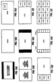
- FIGURES 1(a)-1(i) are useful for explaining different display formats of a wide screen television.
- FIGURE 2 is a block diagram of a wide screen television in accordance with aspects of this invention and adapted for operation at 2f H horizontal scanning.
- FIGURES 3 is a block diagram of the wide screen processor shown in FIGURE 2.
- FIGURE 4 is a block diagram showing further details of the wide screen processor shown in FIGURE 3.
- FIGURE 5 is a block diagram of the picture-in-picture processor shown in FIGURE 4.
- FIGURE 6 is a block diagram of the gate array shown in FIGURE 4 and illustrating the main, auxiliary and output signal paths.
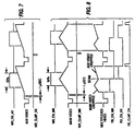
- FIGURES 7 and 8 are timing diagrams useful for explaining the generation of the display format shown in FIGURE 1(d), using fully cropped signals.
- FIGURE 9 is a block diagram showing the main signal path of FIGURE 6 in more detail.
- FIGURE 10 is a block diagram showing the auxiliary signal path of FIGURE 6 in more detail.
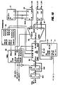
- FIGURE 11 is a block diagram of the timing and control section of the picture-in-picture processor of FIGURE 5.
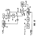
- FIGURE 12 is a block diagram of a circuit for generating the internal 2f H signal in the 1f H to 2f H conversion.
- FIGURE 13 is a combination block and circuit diagram for the deflection circuit shown in FIGURE 2.
- FIGURE 14 is a block diagram of the RGB interface shown in FIGURE 2.
- FIGURES 15 and 16 are pixel diagrams useful for explaining the operation of two-stage variable interpolation filters, as may be used to implement the interpolators of FIGURES 6, 9 and 10.
- FIGURE 17 is a block diagram of a two stage compensated variable interpolation filter.
- FIGURE 18 is a block diagram of a two stage compensated variable interpolation filter configured for implementing a zoom feature.
- FIGURE 19 is a block diagram of a circuit for implementing an eight tap, two stage interpolation filter.
- FIGURE 1 illustrate some, but not all of the various combinations of single and multiple picture display formats which can be implemented according to different inventive arrangements. Those selected for illustration are intended to facilitate the description of particular circuits comprising wide screen televisions according to the inventive arrangements.
- the inventive arrangements are in some cases directed to the display formats themselves, apart from specific underlying circuitry. For purposes of convenience in illustration and discussion herein, a conventional display format ratio of width to height for a video source or signal is generally deemed to be 4 X 3, whereas a wide screen display format ratio of width to height for a video source or signal is generally deemed to be 16 X 9.
- inventive arrangements are not limited by these definitions.
- FIGURE 1(a) illustrates a television, direct view or projection, having a conventional format display ratio of 4 X 3.
- a 16 X 9 format display ratio picture is transmitted, as a 4 X 3 format display ratio signal, black bars appear at the top and at the bottom.
- This is commonly referred to as letterbox format.
- the viewed picture is rather small with respect to the entire available display area.
- the 16 X 9 format display ratio source is converted prior to transmission, so that it will fill the vertical extent of a viewing surface of 4 X 3 format display. However, much information will be cropped from the left and/or right sides.
- the letterbox picture can be expanded vertically but not horizontally, whereby the resulting picture will evidence distortion by vertical elongation. None of the three alternatives is particularly appealing.
- FIGURE 1(b) shows a 16 X 9 screen.
- a 16 X 9 format display ratio video source would be fully displayed, without cropping and without distortion.
- a 16 X 9 format display ratio letterbox picture which is itself in a 4 X 3 format display ratio signal, can be progressively scanned by line doubling or line addition, so as to provide a larger display with sufficient vertical resolution.
- a wide screen television in accordance with this invention can display such a 16 X 9 format display ratio signal whether the main source, the auxiliary Source or an external RGB source.
- FIGURE 1(c) illustrates a 16 X 9 format display ratio main signal in which a 4 X 3 format display ratio inset picture is displayed. If both the main and auxiliary video signals are 16 X 9 format display ratio sources, the inset picture can also have a 16 X 9 format display ratio. The inset picture can be displayed in many different positions.
- FIGURE 1(d) illustrates a display format, wherein the main and auxiliary video signals are displayed with the same size picture.
- Each display area has an format display ratio of 8 X 9, which is of course different from both 16 X 9 and 4 X 3.
- the signal In order to show a 4 X 3 format display ratio source in such a display area, without horizontal or vertical distortion, the signal must be cropped on the left and/or right sides. More of the picture can be shown, with less cropping, if some aspect ratio distortion by horizontal squeezing of the picture is tolerated. Horizontal squeezing results in vertical elongation of objects in the picture.
- the wide screen television according to this invention can provide any mix of cropping and aspect ratio distortion from maximum cropping with no aspect ratio distortion to no cropping with maximum aspect ratio distortion.
- FIGURE 1(e) is a display format wherein a 4 X 3 format display ratio picture is displayed in the center of a 16 X 9 format display ratio screen. Dark bars are evident on the right and left sides.
- FIGURE 1(f) illustrates a display format wherein one large 4 X 3 format display ratio picture and three smaller 4 X 3 format display ratio pictures are displayed simultaneously.
- a smaller picture outside the perimeter of the large picture is sometimes referred to as a POP, that is a picture-outside-picture, rather than a PIP, a picture-in-picture.
- POP picture-outside-picture
- PIP picture-in-picture
- two of the displayed pictures can display movement in real time in accordance with the source.
- the remaining pictures can be displayed in freeze frame format.
- tuners and additional auxiliary signal processing paths can provide for more than two moving pictures. It will also be appreciated that the large picture on the one hand, and the three small pictures on the other hand, can be switched in position, as shown in FIGURE 1(g).
- FIGURE 1(h) illustrates an alternative wherein the 4 X 3 format display ratio picture is centered, and six smaller 4 X 3 format display ratio pictures are displayed in vertical columns on either side.
- a wide screen television provided with two tuners can provide two moving pictures. The remaining eleven pictures will be in freeze frame format.
- FIGURE 1(i) shows a display format having a grid of twelve 4 X 3 format display ratio pictures.
- Such a display format is particularly appropriate for a channel selection guide, wherein each picture is at least a freeze frame from a different channel.
- the number of moving pictures will depend upon the number of available tuners and signal processing paths.
- FIGURE 1 The various formats shown in FIGURE 1 are illustrative, and not limiting, and can be implemented by wide screen televisions shown in the remaining drawings and described in detail below.
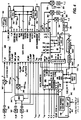
- FIGURE 2 An overall block diagram for a wide screen television in accordance with inventive arrangements, and adapted to operate with 2f H horizontal scanning, is shown in FIGURE 2 and generally designated 10.
- the television 10 generally comprises a video signals input section 20, a chassis or TV microprocessor 216, a wide screen processor 30, a 1f H to 2f H converter 40, a deflection circuit 50, an RGB interface 60, a YUV to RGB converter 240, kine drivers 242, direct view or projection tubes 244 and a power supply 70.
- the grouping of various circuits into different functional blocks is made for purposes of convenience in description, and is not intended as limiting the physical position of such circuits relative to one another.
- the video signals input section 20 is adapted for receiving a plurality of composite video signals from different video sources.
- the video signals may be selectively switched for display as main and auxiliary video signals.
- An RF switch 204 has two antenna inputs ANT1 and ANT 2. These represent inputs for both off-air antenna reception and cable reception.
- the RF switch 204 controls which antenna input is supplied to a first tuner 206 and to a second tuner 208.
- the output of first tuner 206 is an input to a one-chip 202, which performs a number of functions related to tuning, horizontal and vertical deflection and video controls.
- the baseband video signal VIDEO OUT developed in the one-chip and resulting from the signal from first tuner 206 is an input to both video switch 200 and the TV1 input of wide screen processor 30.
- Other baseband video inputs to video switch 200 are designated AUX1 and AUX 2. These might be used for video cameras, laser disc players, video tape players, video games and the like.
- the output of the video switch 200, which is controlled by the chassis or TV microprocessor 216 is designated SWITCHED VIDEO.
- the SWITCHED VIDEO is another input to wide screen processor 30.
- a switch SW1 wide screen processor selects between the TV1 and SWITCHED VIDEO signals as a SEL COMP OUT video signal which is an input to a Y/C decoder 210.
- the Y/C decoder 210 may be implemented as an adaptive line comb filter.
- Two further video sources S1 and S2 are also inputs to the Y/C decoder 210.
- Each of S1 and S2 represent different S-VHS sources, and each consists of separate luminance and chrominance signals.
- a switch which may be incorporated as part of the Y/C decoder, as in some adaptive line comb filters, or which may be implemented as a separate switch, is responsive to the TV microprocessor 216 for selecting one pair of luminance and chrominance signals as outputs designated Y_M and C_IN respectively.
- the selected pair of luminance and chrominance signals is thereafter considered the main signal and is processed along a main signal path.
- Signal designations including _M or _MN refer to the main signal path.
- the chrominance signal C_IN is redirected by the wide screen processor back to the one-chip, for developing color difference signals U_M and V_M.
- U is an equivalent designation for (R-Y)
- V is an equivalent designation for (B-Y).
- the Y_M, U_M, and V_M signals are converted to digital form in the wide screen processor for further signal processing.
- the second tuner 208 functionally defined as part of the wide screen processor 30, develops a baseband video signal TV2.
- a switch SW2 selects between the TV2 and SWITCHED VIDEO signals as an input to a Y/C decoder 220.
- the Y/C decoder 220 may be implemented as an adaptive line comb filter.
- Switches SW3 and SW4 select between the luminance and chrominance outputs of Y/C decoder 220 and the luminance and chrominance signals of an external video source, designated Y_EXT and C_EXT respectively.
- the Y_EXT and C_EXT signals correspond to the S-VHS input S1.
- the Y/C decoder 220 and switches W3 and SW4 may be combined, as in some adaptive line comb filters.
- the output of switches SW3 and SW4 is thereafter considered the auxiliary signal and is processed along an auxiliary signal path.
- the selected luminance output is designated Y_A.
- Signal designations including _A, _AX and _AUX refer to the auxiliary signal path.
- the selected chrominance is converted to color difference signals U_A and V_A.
- the Y_A, U_A and V_A signals are converted to digital form for further signal processing.
- the arrangement of video signal source switching in the main and auxiliary signal paths maximizes flexibility in managing the source selection for the different parts of the different picture display formats.
- a composite synchronizing signal COMP SYNC, corresponding to Y_M is provided by the wide screen processor to a sync separator 212.
- the horizontal and vertical synchronizing components H and V respectively are inputs to a vertical countdown circuit 214.
- the vertical countdown circuit develops a VERTICAL RESET signal which is directed into the wide screen processor 30.
- the wide screen processor generates an internal vertical reset output signal INT VERT RST OUT directed to the RGB interface 60.
- a switch in the RGB interface 60 selects between the internal vertical reset output signal and the vertical synchronizing component of the external RGB source. The output of this switch is a selected vertical synchronizing Component SEL_VERT_SYNC directed to the deflection circuit 50.
- Horizontal and vertical synchronizing signals of the auxiliary video signal are developed by sync separator 250 in the wide screen processor.
- the 1f H to 2f H converter 40 is responsible for converting interlaced video signals to progressively scanned noninterlaced signals, for example one wherein each horizontal line is displayed twice, or an additional set of horizontal lines is generated by interpolating adjacent horizontal lines of the same field. In some instances, the use of a previous line or the use of an interpolated line will depend upon the level of movement which is detected between adjacent fields or frames.
- the converter circuit 40 operates in conjunction with a video RAM 420.
- the video RAM may be used to store one or more fields of a frame, to enable the progressive display.
- the converted video data as Y_2f H , U_2f H and V_2f H signals is supplied to the RGB interface 60.
- the RGB interface 60 shown in more detail in FIGURE 14, enables selection of the converted video data or external RGB video data for display by the video signals input section.
- the external RGB signal is deemed to be a wide format display ratio signal adapted for 2f H scanning.
- the vertical synchronizing component of the main signal is supplied to the RGB interface by the wide screen processor as INT VERT RST OUT, enabling a selected vertical sync (f Vm or f Vext ) to be available to the deflection circuit 50. Operation of the wide screen television enables user selection of an external RGB signal, by generating an internal/external control signal INT/EXT.
- the RGB interface circuit detects an external synchronizing signal, in order to override the selection of a non-existent external RGB input.
- the WSP microprocessor 340 also supplies color and tint controls for the external RGB signal.
- the wide screen processor 30 comprises a picture in picture processor 320 for special signal processing of the auxiliary video signal.
- the term picture-in-picture is sometimes abbreviated as PIP or pix-in-pix.
- a gate array 300 combines the main and auxiliary video signal data in a wide variety of display formats, as shown by the examples of FIGURES 1(b) through 1(i).
- the picture-in-picture circuit 320 and gate array 300 are under the control of a wide screen microprocessor (WSP ⁇ P) 340.
- Microprocessor 340 is responsive to the TV microprocessor 216 over a serial bus.
- the serial bus includes four signal lines, for data, clock signals, enable signals and reset signals.
- the wide screen processor 30 also generates a composite vertical blanking/reset signal, as a three level sandcastle signal.
- the vertical blanking and reset signals can be generated as separate signals.
- a composite blanking signal is supplied by the video signal input section to the RGB interface.
- the deflection circuit 50 receives a vertical reset signal from the wide screen processor, a selected 2f H horizontal synchronizing signal from the RGB interface 60 and additional control signals from the wide screen processor. These additional control signals relate to horizontal phasing, vertical size adjustment and east-west pin adjustment.
- the deflection circuit 50 supplies 2f H flyback pulses to the wide screen processor 30, the 1f H to 2f H converter 40 and the YUV to RGB converter 240.
- Operating voltages for the entire wide screen television are generated by a power supply 70 which can be energized by an AC mains supply.
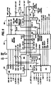
- the wide screen processor 30 is shown in more detail in FIGURE 3.
- the principal components of the wide screen processor are a gate array 300, a picture-in-picture circuit 301, analog to digital and digital to analog converters, the second tuner 208, a wide screen processor microprocessor 340 and a wide screen output encoder 227. Further details of the wide screen processor, which are in common with both the 1f H and the 2f H chassis, for example the PIP circuit, are shown in FIGURE 4.
- a picture-in-picture processor 320 which forms a significant part of the PIP circuit 301, is shown in more detail in FIGURE 5.
- the gate array 300 is shown in more detail in FIGURE 6. A number of the components shown in FIGURE 3, forming parts of the main and auxiliary signal paths, have already been described in detail.
- the second tuner 208 has associated therewith an IF stage 224 and an audio stage 226.
- the second tuner 208 also operates in conjunction with the WSP ⁇ P 340.
- the WSP ⁇ P 340 comprises an input output I/O section 340A and an analog output section 340B.
- the I/O section 340A provides tint and color control signals, the INT/EXT signal for selecting the external RGB video source and control signals for the switches SW1 through SW6.
- the I/O section also monitors the EXT SYNC DET signal from the RGB interface to protect the deflection circuit and cathode ray tube(s).
- the analog output section 340B provides control signals for vertical size, east-west adjust and horizontal phase, through respective interface circuits 254, 256 and 258.
- the gate array 300 is responsible for combining video information from the main and auxiliary signal paths to implement a composite wide screen display, for example one of those shown in the different parts of FIGURE 1.
- Clock information for the gate array is provided by phase locked loop 374, which operates in conjunction with low pass filter 376.
- the main video signal is supplied to the wide screen processor in analog form, and Y U V format, as signals designated Y_M, U_M and V_M. These main signals are converted from analog to digital form by analog to digital converters 342 and 346, shown in more detail in FIGURE 4.
- the color component signals are referred to by the generic designations U and V, which may be assigned to either R-Y or B-Y signal, or I and Q signals
- the sampled luminance bandwidth is limited to 8 MHz because the system clock rate is 1024f H , which is approximately 16 MHz.
- a single analog to digital converter and an analog switch can be used to sample the color component data because the U and V signals are limited to 500 KHz, or 1.5 MHz for wide I.
- the select line UV_MUX for the analog switch, or multiplexer 344 is an 8 MHz signal derived by dividing the system clock by 2.
- a one clock wide start of line SOL pulse synchronously resets this signal to zero at the beginning of each horizontal video line.
- the UV_MUX line than toggles in state each clock cycle through the horizontal line.
- the state of the UV_MUX since the line length is an even number of clock cycles, the state of the UV_MUX, once initialized, will consistently toggle 0, 1, 0, 1, . . ., without interruption.
- the Y and UV data streams out of the analog to digital converters 342 and 346 are shifted because the analog to digital converters each have 1 clock cycle of delay.
- the clock gating information from the interpolator control 349 of main signal processing path 304 must be similarly delayed. Were the clock gating information not delayed, the UV data will not be correctly paired when deleted. This is important because each UV pair represents one vector. A U element from one vector cannot be paired with a V element from another vector without causing a color shift.
- V sample from a previous pair will be deleted along with the current U sample.
- This method of UV multiplexing is referred to as 2:1:1, as there are two luminance samples for every pair of color component (U, V) samples.
- the Nyquist frequency for both U and V is effectively reduced to one half of the luminance Nyquist frequency. Accordingly, the Nyquist frequency of the output of the analog to digital converter for the luminance component is 8 MHz, whereas the Nyquist frequency of the output of the analog to digital converter for the color components is 4 MHz.
- the PIP circuit andlor the gate array may also include means for enhancing the resolution of the auxiliary data notwithstanding the data compression.
- a number of data reduction and data restoration schemes have been developed, including for example paired pixel compression and dithering and dedithering. Moreover, different dithering sequences involving different numbers of bits and different paired pixel compressions involving different numbers of bits are contemplated.
- One of a number of particular data reduction and restoration schemes can be selected by the WSP ⁇ P 340 in order to maximize resolution of the displayed video for each particular kind of picture display format.
- the gate array includes interpolators which operate in conjunction with line memories, which may be implemented as FIFO's 356 and 358.
- the interpolator and FIFO's are utilized to resample the main signal as desired.
- An additional interpolator can resample the auxiliary signal.
- Clock and synchronizing circuits in the gate array control the data manipulator of both the main and auxiliary signals, including the combination thereof into a single output video signal having Y_MX, U_MX and V_MX components. These output components are converted to analog form by digital to analog converters 360, 362 and 364.
- the analog form signals, designated Y, U and V are supplied to the 1f H to 2f H converter 40 for conversion to noninterlaced scanning.
- the Y, U and V signals are also encoded to Y/C format by encoder 227 to define a wide format ratio output signal Y_OUT_EXT/C_OUT_EXT available at panel jacks.
- Switch SW5 selects a synchronizing signal for the encoder 227 from either the gate array, C_SYNC_MN, or from the PIP circuit, C_SYNC_AUX.
- Switch SW6 selects between Y_M and C_SYNC_AUX as synchronizing signal for the wide screen panel output.
- Phase comparator 228 is part of a phase locked loop including low pass filter 230, voltage controlled oscillator 232, divider 234 and capacitor 236.
- the voltage controlled oscillator 232 operates at 32f H, responsive to a ceramic resonator or the like 238.
- the output of the voltage controlled oscillator is divided by 32 to provide a proper frequency second input signal to phase comparator 228.
- the output of the divider 234 is a 1f H REF timing signal.
- the 32f H REF and 1f H REF timing signals are supplied to a divide by 16 counter 400.
- a 2f H output is supplied to a pulse width circuit 402.
- Presetting divider 400 by the 1f H REF signal assures that the divider operates synchronously with the phase locked loop of the video signals input section.
- Pulse width circuit 402 assures that a 2f H -REF signal will have an adequate pulse width to assure proper operation of the phase comparator 404, for example a type CA1391, which forms part of a second phase locked loop including low pass filter 406 and 2f H voltage controlled oscillator 408.
- Voltage controlled oscillator 408 generates an internal 2f H timing signal, which is used for driving the progressively scanned display.
- the other input signal to phase comparator 404 is the 2f H flyback pulses or a timing signal related thereto.
- phase locked loop including phase comparator 404 is useful for assuring that each 2f H scanning period is symmetric within each 1f H period of the input signal. Otherwise, the display may exhibit a raster split, for example, wherein half of the video lines are shifted to the right and half of the video lines are shifted to the left.
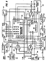
- the deflection circuit 50 is shown in more detail in FIGURE 13.
- a circuit 500 is provided for adjusting the vertical size of the raster, in accordance with a desired amount of vertical overscan necessary for implementing different display formats.
- a constant current source 502 provides a constant quantity of current I RAMP which charges a vertical ramp capacitor 504.
- a transistor 506 is coupled in parallel with the vertical ramp capacitor, and periodically discharges the capacitor responsive to the vertical reset signal.
- current I RAMP provides the maximum available vertical size for the raster. This might correspond to the extent of vertical overscan needed to fill the wide screen display by an expanded 4 X 3 format display ratio signal source, as shown in FIGURE 1(a).
- an adjustable current source 508 diverts a variable amount of current I ADJ from I RAMP , so that vertical ramp capacitor 504 charges more slowly and to a smaller peak value.
- Variable current source 508 is responsive to a vertical size adjust signal, for example in analog form, generated by a vertical size control circuit.
- Vertical size adjustment 500 is independent of a manual vertical size adjustment 510, which may be implemented by a potentiometer or back panel adjustment knob. In either event, the vertical deflection coil(s) 512 receive(s) driving current of the proper magnitude.
- Horizontal deflection is provided by phase adjusting circuit 518, East-West pin correction circuit 514, a 2f H phase locked loop 520 and horizontal output circuit 516.
- the RGB interface circuit 60 is shown in more detailed in FIGURE 14.
- the signal which is to be ultimately displayed will be selected between the output of the 1f H to 2f H converter 40 and an external RGB input.
- the external RGB input is presumed to be a wide format display ratio, progressively scanned source.
- the external RGB signals and a composite blanking signal from the video signals input section 20 are inputs to an RGB to Y U V converter 610.
- the external 2f H composite synchronizing signal for the external RGB signal is an input to external synchronizing signal separator 600.
- Selection of the vertical synchronizing signal is implemented by switch 608.
- Selection of the horizontal synchronizing signal is implemented by switch 604.
- Selection of the video signal is implemented by switch 606.
- Each of the switches 604, 606 and 608 is responsive to an internal/external control signal generated by the WSP ⁇ P 340.
- Selection of internal or external video sources is a user selection. However, if a user inadvertently selects an external RGB source, when no such source is connected or turned on, or if the external source drops out, the vertical raster will collapse, and serious damage to the cathode ray tube(s) can result. Accordingly, an external synchronizing detector 602 checks for the presence of an external synchronizing signal. In the absence of such a signal, a switch override control signal is transmitted to each of switches 604, 606 and 608, to prevent selection of the external RGB source if the signal therefrom is not present.
- the RGB to YUV converter 610 also receives tint and color control signals from the WSP ⁇ P 340.
- a wide screen television in accordance with the inventive arrangements can be implemented with 1f H horizontal scanning instead of 2f H horizontal scanning, although such a circuit is not illustrated.
- a 1f H circuit would not require the 1f H to 2f H converter and the RGB interface. Accordingly, there would be no provision for displaying an external wide format display ratio RGB signal at a 2f H scanning rate.
- the wide screen processor and picture-in-picture processor for a 1f H circuit would be very similar.
- the gate array could be susbtantially identical, although not all of the inputs and outputs would be utilized.
- the various resolution enhancement schemes described herein can be generally applied without regard to whether the television operates with 1f H or 2f H scanning.
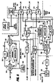
- FIGURE 4 is a block diagram showing further details of the wide screen processor 30 shown in FIGURE 3 which would be the same for both a 1f H and 2f H chassis.
- the Y_A, U_A and V_A signals are an input to the picture in picture processor 320, which can include a resolution processing circuit 370.
- the wide screen television according to aspects of this invention can expand and compress video.
- the special effects embodied by the various composite display formats illustrated in part in FIGURE 1 are generated by the picture-in-picture processor 320, which can receive resolution processed data signals Y_RP, U_RP and V_RP from resolution processing circuit 370. Resolution processing need not be utilized at all times, but during selected display formats.
- the picture-in-picture processor 320 is shown in more detail in FIGURE 5.
- the principal components of the picture-in-picture processor are an analog-to-digital converter section 322, an input section 324, a fast switch (FSW) and bus section 326, a timing and control section 328 and a digital-to-analog converter section 330.
- the timing and control section 328 is shown in more detail in FIGURE 9.
- the picture-in-picture processor 320 may be embodied as an improved variation of a basic CPIP chip developed by Thomson Consumer Electronics, Inc.
- the basic CPIP chip is described more fully in a publication entitled The CTC 140 Picture in Picture (CPIP) Technical Training Manual, available from Thomson Consumer Electronics, Inc., Indianapolis, Indiana.
- the basic special effect is a large picture having a small picture overlaying a portion thereof as shown in FIGURE 1(c).
- the large and small pictures can result from the same video signal, from different video signals and can be interchanged or swapped. Generally speaking, the audio signal is switched to always correspond to the big picture.
- the small picture can be moved to any position on the screen or can step through a number of predetermined positions.
- a zoom feature increases and decreases the size of the small picture, for example to any one of a number of preset sizes.
- the large and small pictures are in fact the same size.
- a user can zoom in on the content of the single picture, for example, in steps from a ratio of 1.0:1 to 5.0:1. While in the zoom mode a user may search or pan through the picture content enabling the screen image to move across different areas of the picture. In either event, either the small picture or the large picture or the zoomed picture can be displayed in freeze frame (still picture format). This function enables a strobe format, wherein the last nine frames of video can be repeated on the screen. The frame repetition rate can be changed from thirty frames per second to zero frames per second.
- the picture-in-picture processor used in the wide screen television differs from the present configuration of the basic CPIP chip itself as described above. If the basic CPIP chip were used with a television having a 16 X 9 screen, and without a video speed up circuit, the inset pictures would exhibit aspect ratio distortion, due to the effective 4 / 3 times horizontal expansion resulting from scanning across the wider 16 X 9 screen. Objects in the picture would be horizontally elongated. If an external speed up circuit were utilized, there would be no aspect ratio distortion, but the picture would not fill the entire screen.
- the picture-in-picture processor 320 is adapted for asymmetrically compressing the video data in one of a plurality of display modes.
- this mode of operation the pictures are compressed 4:1 in the horizontal direction and 3:1 in the vertical direction.
- This asymmetric mode of compression produces aspect ratio distorted pictures for storage in the video RAM. Objects in the pictures are squeezed horizontally. However, if these pictures are read out normally, as for example in the channel scan mode, for display of a 16 X 9 format display ratio screen, the pictures appear correct. The picture fills the screen and there is no aspect ratio distortion.
- the asymmetric compression mode according to this aspect of the invention makes it possible to generate the special display formats on a 16 X 9 screen without external speed up circuitry.
- FIGURE 11 is a block diagram of the timing and control section 328 of the picture-in-picture processor, for example a modified version of the CPIP chip described above, which includes a decimation circuit 328C for implementing the asymmetric compression as one of a plurality of selectable display modes.
- the remaining display modes can provide auxiliary pictures of different sizes.
- Each of horizontal and vertical decimation circuits comprises a counter which is programmed for a compression factor from a table of values under the control of the WSP ⁇ P 340.
- the range of values can be 1:1, 2:1, 3:1 and so on.
- the compression factors can be symmetric or asymmetric, depending upon how the table is set up. Control of the compression ratios can also be implemented by fully programmable, general purpose decimation circuits under the control of the WSP ⁇ P 340.
- the picture-in-picture processor in conjunction with a free running oscillator 348 will take Y/C input from a decoder, for example an adaptive line comb filter, decode the signal into Y, U, V color components and generate horizontal and vertical sync pulses.
- a decoder for example an adaptive line comb filter
- These signals are processed in the picture-in-picture processor for the various full screen modes such as zoom, freeze and channel scan.
- the horizontal and vertical sync present from the video signals input section will have many discontinuities because the signals sampled (different channels) will have non-related sync pulses and will be switched at seemingly random moments in time. Therefore the sample clock (and read/write video RAM clock) is determined by the free running oscillator.
- the sample clock will be locked to incoming video horizontal sync, which in these special cases is the same as the display clock frequency.
- Y, U, V and C_SYNC composite sync outputs from the picture-in-picture processor in analog form can be re-encoded into Y/C components by encode circuit 366, which operates in conjunction with a 3.58 MHz oscillator 380.
- This Y/C_PIP_ENC signal may be connected to a Y/C switch, not shown, which enables the re-encoded Y/C components to be substituted for the Y/C components of the main signal.
- the PIP encoded Y, U, V and sync signals would be the basis for horizontal and vertical timing in the rest of the chassis. This mode of operation is appropriate for implementing a zoom mode for the PIP, based upon operation of the interpolator and FIFO's in the main signal path.
- the picture-in-picture processor 320 comprises analog to digital converting section 322, input section 324, fast switch FSW and bus control section 326, timing and control section 328 and digital to analog converting section 330.
- the picture-in-picture processor 320 digitizes the video signal into luminance (Y) and color difference signals (U, V), subsampling and storing the results in a 1 megabit video RAM 350 as explained above.
- the video RAM 350 associated with the picture-in-picture processor 320 has a memory capacity of 1 megabit, which is not large enough to store a full field of video data with 8-bit samples. Increased memory capacity tends to be expensive and can require more complex management circuitry.
- the smaller number of bits per sample in the auxiliary channel represents a reduction in quantization resolution, or bandwidth, relative to the main signal, which is processed with 8-bit samples throughout.
- This effective reduction of bandwidth is not usually a problem when the auxiliary displayed picture is relatively small, but can be troublesome if the auxiliary displayed picture is larger, for example the same size as the main displayed picture.
- Resolution processing circuit 370 can selectively implement one or more schemes for enhancing the quantization resolution or effective bandwidth of the auxiliary video data.
- a number of data reduction and data restoration schemes have been developed, including for example, paired pixel compression and dithering and dedithering.
- a dedithering circuit would be operatively disposed downstream of the video RAM 350, for example in the auxiliary signal path of the gate array, as explained in more detail below.
- the luminance and color difference signals are stored in an 8:1:1 six-bit Y, U ,V fashion. In other words, each component is quantized into six-bit samples. There are eight luminance samples for every pair of color difference samples.
- the picture-in-picture processor 320 is operated in a mode whereby incoming video data is sampled with a 6404f H clock rate locked to the incoming auxiliary video synchronizing signal instead. In this mode, data stored in the video RAM is orthogonally sampled. When the data is read out of the picture-in-picture processor video RAM 350, it must also be read using the same 640f H clock locked to the incoming auxiliary video signal in order to maintain the orthogonal relationship.
- two four bit latches 352A and 352B are used to recombine the 8-bit data blocks from the vide RAM 4-bit output port.
- the four bit latches also reduce the data clock rate from 1280f H to 640f H .
- the video display and deflection system is synchronized with the main video signal.
- the main video signal must be speeded up, as explained above, to fill the wide screen display.
- the auxiliary video signal must be vertically synchronized with the first video signal and the video display.
- the auxiliary video signal can be delayed by a fraction of a field period in a field memory, and then expanded in a line memory. Synchronization of the auxiliary video data with main video data is accomplished by utilizing the video RAM 350 as a field memory and a first in first out (FIFO) line memory device 354 for expanding the signal.
- the size of FIFO 354 is 2048 X 8.
- the size of FIFO is related to the minimum line storage capacity thought to be reasonably necessary to avoid read/write pointer collisions.
- Read/write pointer collisions occur when old data is read out of the FIFO before new data has an opportunity to be written into the FIFO. Read/write pointer collisions also occur when new data overwrites the memory before the old data has an opportunity to be read out of the FIFO.
- the 8-bit DATA_PIP data blocks from video RAM 350 are written into 2048 x 8 FIFO 354 with the same picture-in-picture processor 640f H clock which was used to sample the video data, that is, the 640f H clock which is locked to the auxiliary signal, rather than the main signal.
- the FIFO 354 is read using the display clock of 1024f H , which is locked to horizontal synchronizing component of the main video channel.
- the use of a multiple line memory (FIFO) which has independent read and write port clocks enables data which was orthogonally sampled at a first rate to be displayed orthogonally at a second rate.
- the asynchronous nature of the read and write clocks does require that steps be undertaken to avoid read/write pointer collisions.
- the main signal path 304, auxiliary signal path 306 and output signal path 312 of the gate array 300 are shown in block diagram form in FIGURE 6.
- the gate array also comprises a clocks/sync circuit 320 and a WSP ⁇ P decoder 310. Data and address output lines of the WSP ⁇ P decoder 310, identified as WSP DATA, are supplied to each of the main circuits and paths identified above, as well as to the picture-in-picture processor 320 and resolution processing circuit 370. It will be appreciated that whether or not certain circuits are, or are not, defined as being part of the gate array is largely a matter of convenience for facilitating explanation of the inventive arrangements.
- the gate array is responsible for expanding, compressing and cropping video data of the main video channel, as and if necessary, to implement different picture display formats.
- the luminance component Y_MN is stored in a first in first out (FIFO) line memory 356 for a length of time depending on the nature of the interpolation of the luminance component.
- the combined chrominance components U/V_MN are stored in FIFO 358.
- Auxiliary signal luminance and chrominance components Y_PIP, U_PIP and V_PIP are developed by demultiplexer 355.
- the luminance component undergoes resolution processing, as desired, in circuit 357, and is expanded as necessary by interpolator 359, generating signal Y_AUX as an output.
- the auxiliary display will be as large as the main signal display, as shown for example in FIGURE 1(d).
- the memory limitations associated with the picture-in-picture processor and video RAM 350 can provide an insufficient number of data points, or pixels for filling such a large display area.
- resolution processing circuit 357 can be used to restore pixels to the auxiliary video signal to replace those lost during data compression, or reduction.
- the resolution processing may correspond to the resolution processing undertaken by circuit 370 shown in FIGURE 4.
- circuit 370 may be a dithering circuit and circuit 357 may be a dedithering circuit.
- the auxiliary video input data is sampled at a 640f H rate and stored in video RAM 350.
- the auxiliary data is read out of video RAM 350 is designated VRAM_OUT.
- the PIP circuit 301 also has the capability of reducing the auxiliary picture by equal integer factors horizontally and vertically, as well as asymmetrically.
- the auxiliary channel data is buffered and synchronized to the main channel digital video by the 4 bit latches 352A and 352B, the auxiliary FIFO 354, timing circuit 369 and synchronization circuit 368.
- the VRAM_OUT data is sorted into Y (luminances), U, V (color components), and FSW_DAT (fast switch data) by demultiplexer 355.
- the FSW_DAT indicates which field type was written into the video RAM.
- the PIP_FSW signal is received directly from the PIP circuit and applied to the output control circuit 321 to determine which field read out of video RAM is to be displayed during the small picture modes.
- the auxiliary channel is sampled at 640f H rate while the main channel is sampled at a 1024f H rate.
- the auxiliary channel FIFO 354 converts the data from the auxiliary channel sample rate to the main channel clock rate.
- the video signal undergoes an 8 / 5 ( 1024 / 640 ) compression. This is more than the 4/ 3 compression necessary to correctly display the auxiliary channel signal. Therefore, the auxiliary channel must be expanded by the interpolator 359 to correctly display a 4 X 3 small picture.
- the interpolator 359 is controlled by interpolator control circuit 371, which is itself responsive to WSP ⁇ P 340.
- the amount of interpolator expansion required is 5 / 6 .
- the chrominance components U_PIP and V_PIP are delayed by circuit 367 far a length of time depending on the nature of the interpolation of the luminance component, generating signals U_AUX and V_AUX as outputs.
- the respective Y, U and V components of the main and auxiliary signals are combined in respective multiplexers 315, 317 and 319 in the output signal path 312, by controlling the read enable signals of the FIFO's 354, 356 and 358.
- the multiplexers 315, 317 and 319 are responsive to output multiplexer control circuit 321.
- Output multiplexer control circuit 321 is responsive to the clock signal CLK, the start of line signal SOL, the H_COUNT signal, the vertical blanking reset signal and the output of the fast switch from the picture-in-picture processor and WSP ⁇ P 340.
- the multiplexed luminance and chrominance components Y_MX, U_MX and V_MX are supplied to respective digital/analog converters 360, 362 and 364 respectively.
- the digital to analog converters are followed by low pass filters 361, 363 and 365 respectively, shown in FIGURE 4.
- the various functions of the picture-in-picture processor, the gate array and the data reduction circuit are controlled by WSP ⁇ P 340.
- the WSP ⁇ P 340 is responsive to the TV ⁇ P 216, being connected thereto by a serial bus.
- the serial bus may be a four wire bus as shown, having lines for data, clock signals, enable signals and reset signals.
- the WSP ⁇ P 340 communicates with the different circuits of the gate array through a WSP ⁇ P decoder 310.
- the video can be expanded to perform horizontal zooming operations usually accompanied by vertical zooming. Horizontal zoom operations up to 33% can be accomplished by reducing compressions to less than 4/3.
- a sample interpolator is used to recalculate the incoming video to a new pixel positions because the luminance video bandwidth, up to 5.5 MHz for S-VHS format, occupies a large percentage of the Nyquist fold over frequency, which is 8 MHz for a 1024f H clock.
- the luminance data Y_MN is routed through an interpolator 337 in the main signal path 304 which recalculates sample values based on the compression or the expansion of the video.
- the function of the switches or route selectors 323 and 331 is to reverse the topology of the main signal path 304 with respect to the relative positions of the FIFO 356 and the interpolator 337. In particular, these switches select whether the interpolator 337 precedes the FIFO 356, as required for compression, or whether the FIFO 356 precedes the interpolator 337, as required for expansion.
- the switches 323 and 331 are responsive to a route control circuit 335, which is itself responsive to the WSP ⁇ P 340. It will be remembered that during small picture modes the auxiliary video signal is compressed for storage in the video RAM 350, and only expansion is necessary for practical purposes. Accordingly, no comparable switching is required in the auxiliary signal path.
- the switch 323 is implemented by two multiplexers 325 and 327.
- Switch 331 is implemented by multiplexer 333.
- the three multiplexers are responsive to the route control circuit 335, which is itself responsive to the WSP ⁇ P 340.
- a horizontal timing/synchronization circuit 339 generates timing signals controlling the writing and reading of the FIFOs, as well as latches 347 and 351, and multiplexer 353.
- the clock signal CLK and start of line signal SOL are generated by the clocks/sync circuit 320.
- An analog to digital conversion control circuit 369 is responsive to Y_MN. the WSP ⁇ P 340 and the most significant bit of UV_MN.
- An interpolator control circuit 349 generates intermediate pixel position values (K), interpolator compensation filter weighting (C) and clock gating information CGY for the luminance and CGUV for the color components. It is the clock gating information which pauses (decimates) or repeats the FIFO data to allow samples not to be written on some clocks for effecting compression or some samples to be read multiple times for expansion.
- a WR_EN_MN_Y signal enables data to be written into the FIFO 356. Every fourth sample can be inhibited from being written into the FIFO. This constitutes a 4/3 compression. It is the function of the interpolator 337 to recalculate the luminance samples being written into the FIFO so that the data read out of the FIFO is smooth, rather than jagged. Expansions may be performed in exactly the opposite manner as compressions.
- the write enable signal has clock gating information attached to it in the form of inhibit pulses. For expanding data, the clock gating information is applied to the read enable signal.
- the clock gating operations may be performed in a synchronous manner. If a switchable video data topology were not used to interchange the positions of the interpolator and FIFO, the read or write clocks would need to be double clocked to pause or repeat the data.
- double clocked means that two data points must be written into the FIFO in a single clock cycle or read from the FIFO during a single clock cycle. The resulting circuitry cannot be made to operate synchronously with the system clock, since the writing or reading clock frequency must be twice as high as the system clock frequency.
- the switchable topology requires only one interpolator and one FIFO to perform both compressions and expansions. If the video switching arrangement described herein were not used, the double clocking situation can be avoided only by using two FIFO's to accomplish the functionality of both compression and expansion. One FIFO for expansions would need to be placed in front of the interpolator and one FIFO for compressions would need to be placed after the interpolator.
- the PIP circuit 301 manipulates a 6 bit Y, U, V, 8:1:1 field memory, video RAM 350, to store incoming video data.
- the video RAM 350 holds two fields of video data in a plurality of memory locations. Each memory location holds eight bits of data. In each 8-bit location there is one 6-bit Y (luminance) sample (sampled at 640f H ) and 2 other bits. These two other bits hold either fast switch data (FSW_DAT) or part of a U or V sample (sampled at 80f H ).
- the FSW_DAT values indicate which type of field was written into video RAM.
- the PIP circuit 301 will determine which field will be read out of the memory to be displayed through the use of the fast switch data. The PIP circuit always reads the opposite field type that is being written to overcome a motion tear problem. If the field type being read is the opposite type than that being displayed, then the even field stored in the video RAM is inverted by deleting the top line of the field when the field is read out of memory. The result is that the small picture maintains correct interlace without a motion tear.
- the clocks/sync circuit 320 generates read, write and enable signals needed for operating FIFOs 354, 356 and 358.
- the FIFOs for the main and auxiliary channels are enabled for writing data into storage for those portions of each video line which is required for subsequent display. Data is written from one of the main or auxiliary channels, but not both, as necessary to combine data from each source on the same video line or lines of the display.
- the FIFO 354 of the auxiliary channel is written synchronously with the auxiliary video signal, but is read out of memory synchronously with the main video signal.
- the main video signal components are read into the FIFOs 356 and 358 synchronously with the main video signal, and are read out of memory synchronously with the main video. How often the read function is switched back and forth between the main and auxiliary channels is a function of the particular special effect chosen.
- FIGURES 7 and 8 The process for this display format is illustrated in FIGURES 7 and 8.
- each of the FIFOs the video data is buffered to be read out at a particular point in time.
- the active region of time where the data may be read out from each FIFO is determined by the display format chosen.
- the main channel video is being displayed on the left hand half of the display and the auxiliary channel video is displayed on the right hand half of the display.
- the arbitrary video portions of the waveforms are different for the main and auxiliary channels as illustrated.
- the read enable control signal (RD_EN_MN) of the main channel 910 x 8 FIFOs is active for 50% of the display active line period of the display beginning with the start of active video, immediately following the video back porch.
- auxiliary channel read enable control signal (RD_EN_AX) is active for the other 50% of the display active line period beginning with the falling edge of the RD_EN_MN signal and ending with the beginning of the main channel video front porch. It may be noted that write enable control signals are synchronous with their respective FIFO input data (main or auxiliary) while the read enable control signals are synchronous with the main channel video.
- the display format shown in FIGURE 1(d) is particularly desirable as it enables two nearly full field pictures to displayed in a side by side format.
- the display is particularly effective and appropriate for a wide format display ratio display, for example 16 X 9.
- Most NTSC signals are represented in a 4 X 3 format, which of course corresponds to 12 x 9.
- Two 4 X 3 format display ratio NTSC pictures may be presented on the same 16 X 9 format display ratio display, either by cropping the pictures by 33% or squeezing the pictures by 33%, and introducing aspect ratio distortion.
- the ratio of picture cropping to aspect ratio distortion may be set any where in between the limits of 0% and 33%.
- two side by side pictures may be presented as 16.7 % squeezed and 16.7% cropped.
- the horizontal display time for a 16 X 9 format display ratio display is the same as a 4 X 3 format display ratio display, because both have 62.5 microsecond nominal line length. Accordingly, an NTSC video signal must be sped up by a factor of 4 / 3 to preserve a correct aspect ratio, without distortion.
- Variable interpolators are utilized in accordance with aspects of this invention to speed up the video signals. In the past, FIFOs having different clock rates at the inputs and outputs have been used to perform a similar function.
- each picture must be distorted or cropped, or some combination thereof, by 50%. A speed up comparable to that needed for a wide screen application is unnecessary.
- the wide screen television can expand and compress video in the horizontal direction by using adaptive interpolator filters.
- the interpolators for the luminance components of the main and auxiliary signals may be skew correction filters, of the kind described in US-A-4,694,414- Christopher.
- a four point interpolator as described therein, for example, comprises a two point linear interpolator and an associated filter and multiplier connected in cascade to provide amplitude and phase compensation. In total, four adjacent data samples are used to calculate each interpolated point.
- the input signal is applied to the two-point linear interpolator.
- the delay imparted to the input is proportional to the value of a delay control signal (K).
- the amplitude and phase errors of the delayed signal are minimized by the application of a correction signal obtained by an additional filter and multiplier connected in cascade.
- This correction signal provides peaking which equalizes the frequency response of the two point linear interpolation filter for all values of (K).
- the original four point interpolator is optimized for use with signals having a pass band if fs / 4 , where fs is the data sample rate.
- both channels can use what is termed a two stage interpolative process.
- the frequency response of the original variable interpolation filter can be improved by using such a two stage process.
- This process is hereinafter referred to as a two stage interpolator.
- a two stage interpolator according to an inventive arrangement comprises a 2n+4 tap finite impulse response (FIR) filter with fixed coefficients and a four point variable interpolator, as is illustrated by FIGURE 15-16.
- the FIR filter output is spatially located midway between the input pixel samples, as shown in FIGURE 15.
- the output of the FIR filter is then combined by interleaving with the original data samples, which are delayed, to create an effective 2fs sample rate. This is a valid assumption for frequencies in the pass band of the FIR filter. The result is that the effective pass band of the original four point interpolator is significantly increased.
- the compensated variable interpolation filter of the prior art provides accurately interpolated samples as long as the frequency components of the signal are no greater than approximately one fourth the sample rate, 1 / 4 fs.
- the two-stage approach can be used for signals having frequency components substantially greater than 1 / 4 fs, as shown by the block diagram for a two stage interpolator 390 in FIGURE 17.
- a signal DS_A of digital samples at a sampling rate fs is an input to a finite impulse response (FIR) filter, for example a fixed FIR filter 391.
- FIR finite impulse response
- the finite impulse response filter 391 generates from the signal DS_A a second signal DS_B of digital samples which are also at the sampling rate fs, but which are temporally located between the values of the first signal DS_A, for example at the midpoint between each value.
- Signal DS_A is also an input to a delay circuit 392, which produces a signal DS_C of digital samples, identical to signal DS_A but time delayed by (N+1) /fs.
- the data streams DS_B and DS_C are combined by interleaving in multiplexer 393, resulting in a data stream of values DS_D at twice the sampling rate, 2fs.
- Data stream DS_D is an input to a compensated variable interpolator 394.
- the fixed FIR filter is designed to accurately produce sample values corresponding to time locations exactly half-way in between the incoming sample positions. These are then interleaved with delayed but otherwise unmodified samples, producing a data stream with a 2fs sample rate.
- the FIR filter is most conveniently implemented using an even number of symmetrically weighted taps.
- An eight-tap filter for example, having tap weights of: -1 / 32 , 5 / 64 , -11 / 64 , 5 / 8 , 5 / 8 , -11 / 64 , 5 / 64 , -1 / 32 will accurately interpolate signals having frequency components up to about 0.4fs. Since the data rate is doubled to 2fs by the interleaving, the signal being processed by the variable interpolator never contains frequency components higher than 1 / 4 the sample rate.
- An advantage of the two-stage interpolator is to allow accurate interpolations for signals with bandwidths approaching 1 / 2 the sample rate.
- the system is most appropriate for display modes requiring time expansion, such as zoom, where the object is to maintain as much of the original bandwidth as possible.
- This can be pertinent in a wide screen television, particularly in the auxiliary channel, where the auxiliary signal is initially sampled at a fairly low rate, for example 10 MHz. Preserving as much bandwidth as possible can be important.
- a two stage interpolator 390' appropriate for a zoom application is shown in block diagram form in FIGURE 18.
- Components in common with the interpolator 390 shown in FIGURE 17 have the same reference numeral as do the designations of the data streams.
- the object of the two stage interpolator 390' is to zoom the incoming image horizontally by a factor of m, where m is greater than 2.0.
- m is greater than 2.0.
- the signal is stored in a FIFO line memory 395 at fIN rate, and a portion is then read out as data stream DS_A at a reduced rate of fs.
- the fs clock is composed of a subset of fIN clock pulses, and does not have a uniform period.
- Data stream DS_ B corresponding to sample values half-way in between the existing samples of data stream DS_A are estimated using the fixed FIR filter 391, and are then interleaved with the delayed samples of data stream DA_ C to form the double rate data stream DS_D.
- Data steam DS_D having twice the original sample density, is then processed by the variable interpolator 394 to produce a sample value for each fIN period.
- the fractional part controls the variable interpolator by supplying the K value from latch 398.
- the integer carry output (CO) generates the 2fs clock, through latch 397, for reading of the FIFO 395 and shifting data through the FIR filter 391, the delay circuit 392, the multiplexer 393 and the interpolator 394.
- Divider 396 provides the fs signal from the 2fs signal.
- the above two stage interpolator can also be constructed using the 2n+4 FIR filter and a simple linear interpolator without compensation. This is the equivalent of setting the compensation multiplier C, of the four point interpolator, equal to zero.
- a second alternative is using the original four point interpolator along with a fixed weight linear phase 2n+5 tap FIR. In order to accomplish this successfully it is first necessary to optimize the original four point interpolator technique.
- the four point interpolator can be viewed as a variable FIR filter with non-linear phase. It should be recognized that the frequency response of the four point interpolator is highly dependent upon the value K which is chosen.
- K which is chosen.
- Each particular horizontal compression or expansion can be viewed as being made up of the output of several different FIR filters each having their own unique frequency and phase response. Artifacts in the interpolation become apparent when the collective frequency responses of the interpolator diverge. Thus, the overall pass band of a particular horizontal compression or expansion can be optimized by choosing values of K which produce the most equalized frequency response.
- This optimization can be shown by examining the frequency response of a 4 sample to 3 sample data reduction, that is, a 4:3 compression.
- the criteria that will be used to determine when artifacts become unacceptable is the frequency at which the amplitude curves of the individual interpolations diverge by more than 1 dB. Choosing the initial values of K to be 1, 5/16, and 11/16 leads to a usable pass bend of .3 x fs. If the values of K are chosen to be 8/16, 13/16, and 3/16, the useable pass band becomes .35 x fs. This represents a 16.6% improvement. Using this technique, the frequency response of the horizontal interpolator can be equalized.
- K and C can be put into a memory block and, dependent upon the speedup required, a counter can index the read pointer to call out the desired memory location and load K and C into the interpolator multipliers. It is very advantageous, for this reason, to encode the value of C into the value of K, such that a single 4-bit or 5-bit word can convey both K and C values.
- the control signal sends a value of K to the linear interpolator.
- the value of K is decoded to yield a value of C for the compensation network multiplier.
- the FIR coefficients are the multipliers for C in the overall interpolator equations.
- This aspect of the invention can be extended generally to 2n tap FIR filters used as compensation networks, although it can become increasingly more difficult to use only two linear multipliers for calculating the linear interpolation and the associated compensation network.
- FIGURE 19 A block diagram for a specific circuit 1150 for implementing an eight tap, two stage filter using a four point interpolator is shown in FIGURE 19.
- the video luminance signal to be expanded or compressed is an input to a horizontal delay line circuit 1152.
- the outputs of the delay line Z 0 , Z -1 , Z -2 , Z -3 , Z -4 , Z -5 , Z -6 and Z -7 are inputs to an eight tap FIR filter 1154.
- the FIR filter generates at least one set of intermediate samples, designated I, for example between each of the real samples, designated Z. Results can sometimes be improved by using a plurality of FIR filters to generate a plurality of sets of intermediate points, although this significantly increases the complexity of the system.
- Such additional FIR filters are shown by the multiple representations of FIR filter 1154 and Z -1 delay circuit 1158.
- Outputs Z -3 , Z -4 and Z -5 are also inputs to the delay matching circuit 1156.
- the I 0 output is a direct input to a data selecting circuit 1160, as is a version I -1 thereof delayed by circuit 1158.
- the outputs Z- (3+n) , Z- (4+n) and Z- (5+n) are also input to data selector circuit 1160.
- the inputs to data selector circuit 1160 are chosen for being the most symmetric with respect to the delay.
- the number of such inputs is one more than the number of points of the interpolator of the second stage, in this case, a four point interpolator 1162.
- the relative temporal position of the inputs to data selector 1160 is as follows: Z -(3+n) ,I 0 , Z -(4+n) , I -1 , Z -(5+n) .
- Data selector circuit 1160 can be an array of multiplexers, for example, controlled by the MUX_SEL control signal.
- the selectable sets are indicated diagrammatically and are so arranged that each interpolation of the interpolator 1162 is based on two real points and two intermediate points.
- the outputs Y0, Y1, Y2 and Y3 of data selecting circuit 1160 correspond to one of the two selectable sets, and are the inputs to the four point interpolator 1162.
- the MUX_SEL selection depends upon which of the original points the intermediate point falls between.
- the output Yout of the interpolator 1162 which operates responsive to the K and C control values, is an expanded or compressed video luminance signal.
Landscapes
- Engineering & Computer Science (AREA)
- Multimedia (AREA)
- Signal Processing (AREA)
- Physics & Mathematics (AREA)
- General Physics & Mathematics (AREA)
- Theoretical Computer Science (AREA)
- Computer Graphics (AREA)
- Controls And Circuits For Display Device (AREA)
- Television Systems (AREA)
- Studio Circuits (AREA)
- Details Of Television Scanning (AREA)
- Transforming Electric Information Into Light Information (AREA)
- Color Television Systems (AREA)
- Synchronizing For Television (AREA)
- Pinball Game Machines (AREA)
- Organic Low-Molecular-Weight Compounds And Preparation Thereof (AREA)
- Paints Or Removers (AREA)
- Display Devices Of Pinball Game Machines (AREA)
- Image Processing (AREA)
- Sealing Material Composition (AREA)
- Application Of Or Painting With Fluid Materials (AREA)
- Image Analysis (AREA)
- Acyclic And Carbocyclic Compounds In Medicinal Compositions (AREA)
- Signal Processing For Digital Recording And Reproducing (AREA)
- Stereophonic System (AREA)
- Television Signal Processing For Recording (AREA)
- Liquid Crystal Display Device Control (AREA)
- Compositions Of Macromolecular Compounds (AREA)
- Inks, Pencil-Leads, Or Crayons (AREA)
- Manipulator (AREA)
- Control Of Indicators Other Than Cathode Ray Tubes (AREA)
- Testing, Inspecting, Measuring Of Stereoscopic Televisions And Televisions (AREA)
- Two-Way Televisions, Distribution Of Moving Picture Or The Like (AREA)
Applications Claiming Priority (3)
| Application Number | Priority Date | Filing Date | Title |
|---|---|---|---|
| GB909012326A GB9012326D0 (en) | 1990-06-01 | 1990-06-01 | Wide screen television |
| GB9012326 | 1990-06-01 | ||
| PCT/US1991/003734 WO1991019393A1 (en) | 1990-06-01 | 1991-05-29 | Two stage interpolation system |
Publications (3)
| Publication Number | Publication Date |
|---|---|
| EP0532667A1 EP0532667A1 (en) | 1993-03-24 |
| EP0532667A4 EP0532667A4 (en) | 1993-12-22 |
| EP0532667B1 true EP0532667B1 (en) | 1997-08-06 |
Family
ID=10676970
Family Applications (17)
| Application Number | Title | Priority Date | Filing Date |
|---|---|---|---|
| EP91912116A Expired - Lifetime EP0532667B1 (en) | 1990-06-01 | 1991-05-29 | Two stage interpolation system |
| EP01111808A Ceased EP1130909A3 (en) | 1990-06-01 | 1991-05-29 | Field synchronization system maintaining interlace integrity |
| EP91912249A Expired - Lifetime EP0532672B1 (en) | 1990-06-01 | 1991-05-29 | Side by side television pictures |
| EP91910567A Expired - Lifetime EP0532583B1 (en) | 1990-06-01 | 1991-05-29 | Automatic letterbox detection |
| EP97120599A Expired - Lifetime EP0831645B1 (en) | 1990-06-01 | 1991-05-29 | Automatic letterbox detection |
| EP19910921006 Withdrawn EP0532711A4 (en) | 1990-06-01 | 1991-05-29 | Skewing dither sequences |
| EP91910878A Expired - Lifetime EP0533748B1 (en) | 1990-06-01 | 1991-05-29 | Field synchronization system maintaining interlace integrity |
| EP91911604A Expired - Lifetime EP0532652B1 (en) | 1990-06-01 | 1991-05-29 | Wide screen television |
| EP91911605A Expired - Lifetime EP0532653B1 (en) | 1990-06-01 | 1991-05-29 | Field synchronization system with write/read pointer control |
| EP91912590A Revoked EP0532682B1 (en) | 1990-06-01 | 1991-05-29 | Synchronizing side by side pictures |
| EP91910761A Expired - Lifetime EP0533738B1 (en) | 1990-06-01 | 1991-05-29 | Asymmetric picture compression |
| EP91911305A Expired - Lifetime EP0532635B1 (en) | 1990-06-01 | 1991-05-30 | Chrominance processing system |
| EP91910788A Expired - Lifetime EP0532592B1 (en) | 1990-06-01 | 1991-05-30 | Chrominance processing and timing system |
| EP91911041A Expired - Lifetime EP0532615B1 (en) | 1990-06-01 | 1991-05-30 | Picture overlay system for television |
| EP91912342A Expired - Lifetime EP0532676B1 (en) | 1990-06-01 | 1991-05-30 | Aspect ratio control for picture overlays |
| EP91912104A Expired - Lifetime EP0532665B1 (en) | 1990-06-01 | 1991-05-30 | Luminance processing system |
| EP91912548A Expired - Lifetime EP0540548B1 (en) | 1990-06-01 | 1991-05-30 | Vertical zoom and panning for television |
Family Applications After (16)
| Application Number | Title | Priority Date | Filing Date |
|---|---|---|---|
| EP01111808A Ceased EP1130909A3 (en) | 1990-06-01 | 1991-05-29 | Field synchronization system maintaining interlace integrity |
| EP91912249A Expired - Lifetime EP0532672B1 (en) | 1990-06-01 | 1991-05-29 | Side by side television pictures |
| EP91910567A Expired - Lifetime EP0532583B1 (en) | 1990-06-01 | 1991-05-29 | Automatic letterbox detection |
| EP97120599A Expired - Lifetime EP0831645B1 (en) | 1990-06-01 | 1991-05-29 | Automatic letterbox detection |
| EP19910921006 Withdrawn EP0532711A4 (en) | 1990-06-01 | 1991-05-29 | Skewing dither sequences |
| EP91910878A Expired - Lifetime EP0533748B1 (en) | 1990-06-01 | 1991-05-29 | Field synchronization system maintaining interlace integrity |
| EP91911604A Expired - Lifetime EP0532652B1 (en) | 1990-06-01 | 1991-05-29 | Wide screen television |
| EP91911605A Expired - Lifetime EP0532653B1 (en) | 1990-06-01 | 1991-05-29 | Field synchronization system with write/read pointer control |
| EP91912590A Revoked EP0532682B1 (en) | 1990-06-01 | 1991-05-29 | Synchronizing side by side pictures |
| EP91910761A Expired - Lifetime EP0533738B1 (en) | 1990-06-01 | 1991-05-29 | Asymmetric picture compression |
| EP91911305A Expired - Lifetime EP0532635B1 (en) | 1990-06-01 | 1991-05-30 | Chrominance processing system |
| EP91910788A Expired - Lifetime EP0532592B1 (en) | 1990-06-01 | 1991-05-30 | Chrominance processing and timing system |
| EP91911041A Expired - Lifetime EP0532615B1 (en) | 1990-06-01 | 1991-05-30 | Picture overlay system for television |
| EP91912342A Expired - Lifetime EP0532676B1 (en) | 1990-06-01 | 1991-05-30 | Aspect ratio control for picture overlays |
| EP91912104A Expired - Lifetime EP0532665B1 (en) | 1990-06-01 | 1991-05-30 | Luminance processing system |
| EP91912548A Expired - Lifetime EP0540548B1 (en) | 1990-06-01 | 1991-05-30 | Vertical zoom and panning for television |
Country Status (23)
| Country | Link |
|---|---|
| US (2) | US5289284A (enExample) |
| EP (17) | EP0532667B1 (enExample) |
| JP (20) | JP3373509B2 (enExample) |
| KR (16) | KR100190247B1 (enExample) |
| CN (15) | CN1041878C (enExample) |
| AU (15) | AU8084591A (enExample) |
| BR (1) | BR9106539A (enExample) |
| CA (1) | CA2082260C (enExample) |
| DE (19) | DE4191166C2 (enExample) |
| ES (12) | ES2128319T3 (enExample) |
| FI (1) | FI100931B (enExample) |
| GB (2) | GB9012326D0 (enExample) |
| HK (1) | HK1004588A1 (enExample) |
| HU (2) | HUT64662A (enExample) |
| IN (1) | IN177990B (enExample) |
| MY (14) | MY106666A (enExample) |
| PL (1) | PL167644B1 (enExample) |
| PT (13) | PT97813B (enExample) |
| RU (1) | RU2119187C1 (enExample) |
| SG (11) | SG82550A1 (enExample) |
| TR (1) | TR25549A (enExample) |
| TW (3) | TW243575B (enExample) |
| WO (17) | WO1991019395A1 (enExample) |
Families Citing this family (146)
| Publication number | Priority date | Publication date | Assignee | Title |
|---|---|---|---|---|
| US5369444A (en) * | 1990-06-01 | 1994-11-29 | Thomson Consumer Electronics | Field type matching system |
| US5345270A (en) * | 1990-06-01 | 1994-09-06 | Thomson Consumer Electronics, Inc. | Managing letterbox signals with logos and closed captions |
| US5249049A (en) * | 1990-06-01 | 1993-09-28 | Thomson Consumer Electronics, Inc. | Managing letterbox displays |
| US5351135A (en) * | 1990-06-01 | 1994-09-27 | Thomson Consumer Electronics, Inc. | Managing letterbox signals with logos |
| US5309234A (en) * | 1991-05-29 | 1994-05-03 | Thomson Consumer Electronics | Adaptive letterbox detector |
| JPH04365278A (ja) * | 1991-06-13 | 1992-12-17 | Matsushita Electric Ind Co Ltd | 多画面表示回路 |
| US5414463A (en) * | 1991-09-18 | 1995-05-09 | Hitachi, Ltd. | Video cameras capable of switching an aspect ratio and view finders for use in the same |
| JPH05183833A (ja) * | 1992-01-07 | 1993-07-23 | Sony Corp | 表示装置 |
| US5287188A (en) * | 1992-01-07 | 1994-02-15 | Thomson Consumer Electronics, Inc. | Horizontal panning for wide screen television |
| EP0616466B1 (en) * | 1992-01-07 | 2000-06-07 | Thomson Consumer Electronics, Inc. | Horizontal panning for wide screen television |
| GB9200281D0 (en) | 1992-01-08 | 1992-02-26 | Thomson Consumer Electronics | A pip horizontal panning circuit for wide screen television |
| TW220024B (enExample) * | 1992-01-08 | 1994-02-01 | Thomson Consumer Electronics | |
| JPH05236377A (ja) * | 1992-02-18 | 1993-09-10 | Sony Corp | 映像セレクタ |
| GB9205614D0 (en) * | 1992-03-14 | 1992-04-29 | Innovision Ltd | Sample rate converter suitable for converting between digital video formats |
| JP3435172B2 (ja) * | 1992-06-02 | 2003-08-11 | 株式会社東芝 | テレビジョン信号処理回路 |
| DE69222754T2 (de) | 1992-03-27 | 1998-02-26 | Alsthom Cge Alcatel | Videodekoder |
| JP2759727B2 (ja) * | 1992-04-22 | 1998-05-28 | 日本ビクター株式会社 | ディスプレイ装置 |
| GB2254977B (en) * | 1992-04-23 | 1996-01-17 | Philips Electronics Nv | Receiver for letterbox television signals |
| JPH0638128A (ja) * | 1992-06-19 | 1994-02-10 | Sony Corp | 映像表示装置 |
| US5294987A (en) * | 1992-07-10 | 1994-03-15 | Thomson Consumer Electronics, Inc. | Field to field vertical panning system |
| US5262864A (en) * | 1992-07-10 | 1993-11-16 | Thomson Consumer Electronics, Inc. | Frame based vertical panning system |
| TW234806B (enExample) * | 1992-07-10 | 1994-11-21 | Thomson Consumer Electronics | |
| JP3237783B2 (ja) | 1992-08-05 | 2001-12-10 | 株式会社富士通ゼネラル | 2画面表示テレビ受信機 |
| EP0603535A1 (en) * | 1992-11-23 | 1994-06-29 | Thomson Consumer Electronics, Inc. | Tuner signal switching apparatus |
| TW335241U (en) * | 1992-11-30 | 1998-06-21 | Thomson Consumer Electronics | A video display system |
| ES2154291T3 (es) | 1992-12-09 | 2001-04-01 | Discovery Communicat Inc | Controlador de red para sistemas de distribucion de programas de television por cable. |
| US7168084B1 (en) | 1992-12-09 | 2007-01-23 | Sedna Patent Services, Llc | Method and apparatus for targeting virtual objects |
| US9286294B2 (en) | 1992-12-09 | 2016-03-15 | Comcast Ip Holdings I, Llc | Video and digital multimedia aggregator content suggestion engine |
| US5369341A (en) * | 1992-12-11 | 1994-11-29 | Thomson Consumer Electronics, Inc. | Vertical retrace with zoom and centered fast retrace |
| US5614952A (en) | 1994-10-11 | 1997-03-25 | Hitachi America, Ltd. | Digital video decoder for decoding digital high definition and/or digital standard definition television signals |
| TW274673B (enExample) * | 1993-02-10 | 1996-04-21 | Thomson Consumer Electronics | |
| JP3594596B2 (ja) * | 1993-02-17 | 2004-12-02 | トムソン コンシユーマ エレクトロニクス インコーポレイテツド | レターボックスの表示制御 |
| JP3522273B2 (ja) * | 1993-02-17 | 2004-04-26 | トムソン コンシユーマ エレクトロニクス インコーポレイテツド | 適応レターボックス検出器 |
| JPH06311449A (ja) * | 1993-02-26 | 1994-11-04 | Sony Corp | テレビジョン受像機 |
| JP3240210B2 (ja) | 1993-03-10 | 2001-12-17 | トムソン コンシユーマ エレクトロニクス インコーポレイテツド | ビデオシステム |
| EP0656727B1 (en) * | 1993-11-03 | 1999-04-28 | SONY-WEGA PRODUKTIONS GmbH | Teletext receiver |
| SG80518A1 (en) * | 1993-03-15 | 2001-05-22 | Thomson Consumer Electronics | Horizontal panning for wide screen television |
| GB2308266B (en) * | 1993-03-30 | 1997-08-20 | Sony Corp | Video signal display apparatus and video signal processing circuit therefor |
| JPH06292148A (ja) * | 1993-03-30 | 1994-10-18 | Sony Corp | 倍速映像表示装置 |
| CN1050255C (zh) * | 1993-04-03 | 2000-03-08 | 汤姆森消费电子有限公司 | 用于宽屏电视的水平画面摄取系统 |
| CN1042786C (zh) * | 1993-04-21 | 1999-03-31 | 汤姆森消费电子有限公司 | 视频显示控制系统 |
| CN1051896C (zh) * | 1993-04-21 | 2000-04-26 | 汤姆森消费电子有限公司 | 视频显示控制系统 |
| BE1007167A3 (nl) * | 1993-05-13 | 1995-04-11 | Philips Electronics Nv | Zendstation voor het uitzenden van een pluraliteit van televisie programma's, en een ontvanger voor het ontvangen daarvan. |
| US5363143A (en) * | 1993-09-03 | 1994-11-08 | Thomson Consumer Electronics, Inc. | Side by side picture display with reduced cropping |
| US5359267A (en) | 1993-09-03 | 1994-10-25 | Thomson Consumer Electronics, Inc. | Vertical deflection with vertical shrink mode |
| JP3051802B2 (ja) | 1993-09-10 | 2000-06-12 | シャープ株式会社 | 映像信号再生装置 |
| JP3022713B2 (ja) * | 1993-09-30 | 2000-03-21 | 日本ビクター株式会社 | 画像信号処理方法 |
| KR960012492B1 (ko) * | 1993-11-03 | 1996-09-20 | 엘지전자 주식회사 | 와이드 티브이 수상기의 수직 위치 가변회로 |
| SG93754A1 (en) * | 1993-11-26 | 2003-01-21 | Thomson Consumer Electronics | Emulation of computer monitor in a wide screen television |
| JP2554450B2 (ja) * | 1993-12-16 | 1996-11-13 | 日本テレビ放送網株式会社 | フレームシンクロナイザおよびこれを使用した信号切り替え装置 |
| TW312076B (enExample) * | 1993-12-21 | 1997-08-01 | Thomson Consumer Electronics | |
| JPH07184138A (ja) * | 1993-12-24 | 1995-07-21 | Toshiba Corp | 2画面映像処理回路 |
| US5790197A (en) * | 1994-01-12 | 1998-08-04 | Thomson Consumer Electronics,. Inc. | Multimode interpolation filter as for a TV receiver |
| EP0739572B1 (en) * | 1994-01-12 | 2001-05-16 | Thomson Consumer Electronics, Inc. | Video signal decompression system and multimode video up-convertor |
| CN1048138C (zh) * | 1994-01-12 | 2000-01-05 | 汤姆森消费电子有限公司 | 用于电视接收机的多方式内插滤波器 |
| TW307971B (enExample) * | 1994-03-31 | 1997-06-11 | Matsushita Electric Industrial Co Ltd | |
| US5719636A (en) * | 1994-04-28 | 1998-02-17 | Kabushiki Kaisha Toshiba | Letter-box screen detection apparatus |
| EP0697787A3 (de) * | 1994-08-20 | 1996-05-29 | Loewe Opta Gmbh | Verfahren und Schaltungsanordnung zur Darstellung eines 16:9-Fernsehbildes nach dem PAL-Plus-Verfahren auf dem Bildschirm eines Fernsehempfängers mit einer 16:9-formatigen Bildröhre |
| DE4432169A1 (de) * | 1994-09-09 | 1996-03-14 | Bosch Siemens Hausgeraete | Fernsehgerät |
| US5574508A (en) * | 1994-11-02 | 1996-11-12 | Rca Thomson Licensing Corporation | Vertical panning for interlaced video |
| ES2142903T3 (es) * | 1994-12-12 | 2000-05-01 | Sony Wega Produktions Gmbh | Metodo y aparato para visualizar dos imagenes de video simultaneamente. |
| EP0737004A1 (en) * | 1995-04-05 | 1996-10-09 | Thomson Consumer Electronics, Inc. | Field type detector for video signal |
| GB9508289D0 (en) * | 1995-04-24 | 1995-06-14 | Rca Thomson Licensing Corp | Deflection circuits for changing display format on wide screen picture tubes |
| JP3617130B2 (ja) * | 1995-07-21 | 2005-02-02 | ソニー株式会社 | 映像信号処理回路及び画像表示装置 |
| KR100426109B1 (ko) * | 1995-08-09 | 2004-08-16 | 코닌클리케 필립스 일렉트로닉스 엔.브이. | 화상의하단부가이동되는화상디스플레이장치 |
| KR0176825B1 (ko) * | 1995-08-16 | 1999-05-01 | 구자홍 | 티브이의 영상 모드 선택 방법 및 그 장치 |
| CA2184121A1 (en) * | 1995-08-30 | 1997-03-01 | John R. Reder | Sampling analog video signal for secondary images |
| KR0144505B1 (ko) * | 1995-09-18 | 1998-08-17 | 구자홍 | 영상표시기기의 화면 자동 조정장치 및 방법 |
| JPH0993505A (ja) * | 1995-09-26 | 1997-04-04 | Toshiba Corp | 文字多重デコーダを有するテレビ受信機 |
| JPH0993548A (ja) * | 1995-09-27 | 1997-04-04 | Toshiba Corp | 文字情報表示機能付きテレビ受信機 |
| JPH09116821A (ja) * | 1995-10-18 | 1997-05-02 | Toshiba Corp | テレビジョン受像機 |
| FR2742279B1 (fr) * | 1995-12-06 | 1998-01-09 | Thomson Multimedia Sa | Dispositif de decimation de sequences de donnees numeriques |
| US6008860A (en) * | 1995-12-29 | 1999-12-28 | Thomson Consumer Electronics, Inc. | Television system with provisions for displaying an auxiliary image of variable size |
| JP3575153B2 (ja) * | 1996-01-17 | 2004-10-13 | ソニー株式会社 | アスペクト比判別回路及び映像モニタ装置 |
| CA2191632A1 (en) * | 1996-02-13 | 1997-08-14 | James Lee Combs | Video processor for processing two analog composite video signals |
| CN1065396C (zh) * | 1996-02-17 | 2001-05-02 | 明碁电脑股份有限公司 | 宽屏幕电视的屏幕检测系统 |
| DE69606852T2 (de) * | 1996-04-18 | 2000-06-29 | Matsushita Electric Industrial Co., Ltd. | Digitale Signalverarbeitungsschaltung für einen Fernsehempfänger |
| JPH09284671A (ja) * | 1996-04-18 | 1997-10-31 | Toshiba Corp | 走査線変換装置 |
| JPH09326958A (ja) * | 1996-06-05 | 1997-12-16 | Sony Corp | 画像処理装置および処理方法 |
| EP0822711A3 (en) * | 1996-08-02 | 1998-07-01 | SANYO ELECTRIC Co., Ltd. | Internet information displaying apparatus |
| KR100206802B1 (ko) * | 1996-08-20 | 1999-07-01 | 구자홍 | 텔레비젼수상기의 자동 와이드화면 디스플레이 방법 및 장치 |
| KR100678355B1 (ko) * | 1996-09-27 | 2007-05-14 | 소니 가부시끼 가이샤 | 영상표시및제어장치와그의방법 |
| US5854902A (en) * | 1996-10-31 | 1998-12-29 | Sensormatic Electronics Corporation | Video data capture and formatting in intelligent video information management system |
| JP3828992B2 (ja) * | 1996-11-27 | 2006-10-04 | 三星電子株式会社 | セミワイド画面テレビジョン受信機の画面安定化回路 |
| US6064445A (en) * | 1996-11-28 | 2000-05-16 | Samsung Electronics Co., Ltd. | Automatic picture size control method for semiwide-screen television receiver |
| DE19652362A1 (de) * | 1996-12-17 | 1998-06-18 | Thomson Brandt Gmbh | Verfahren und Vorrichtung zur Kompensation der durch die Verarbeitung von Chrominanz-Signalen entstehenden Luminanzdefekte |
| JPH1198422A (ja) * | 1997-09-19 | 1999-04-09 | Sony Corp | 映像信号判別回路 |
| JP3464924B2 (ja) * | 1998-03-13 | 2003-11-10 | 株式会社東芝 | 同期制御回路 |
| US6501507B1 (en) * | 1998-05-13 | 2002-12-31 | Barth Alan Canfield | Multimode interpolation filter as for a TV receiver |
| KR100299759B1 (ko) * | 1998-06-29 | 2001-10-27 | 구자홍 | 영상표시기기의 화면 상태 자동 조정 장치와 방법 |
| GB9817421D0 (en) * | 1998-08-11 | 1998-10-07 | Danmere Limited | Interactive television control/operating system |
| CN1096181C (zh) * | 1998-08-13 | 2002-12-11 | 汤姆森消费电子有限公司 | 视频显示控制系统 |
| DE19911947C2 (de) * | 1999-03-17 | 2003-04-24 | Infineon Technologies Ag | Verfahren zur Farbkantenverbesserung bei einer Bildeinblendung |
| GB2349288B (en) | 1999-04-16 | 2003-10-22 | Quantel Ltd | A video editing system |
| US6791578B1 (en) | 2000-05-30 | 2004-09-14 | Apple Computer, Inc. | 16:9 aspect ratio and anamorphic image processing |
| US7181416B2 (en) * | 2000-06-08 | 2007-02-20 | Blackstone Corporation | Multi-function transaction processing system |
| CN1199452C (zh) * | 2001-06-04 | 2005-04-27 | 华为技术有限公司 | 多路数字图像多组组合的实现方法和总线接口技术 |
| US7793326B2 (en) | 2001-08-03 | 2010-09-07 | Comcast Ip Holdings I, Llc | Video and digital multimedia aggregator |
| US7908628B2 (en) | 2001-08-03 | 2011-03-15 | Comcast Ip Holdings I, Llc | Video and digital multimedia aggregator content coding and formatting |
| US20030204457A1 (en) * | 2002-04-26 | 2003-10-30 | Arias Luis A. | Payee account payment system |
| DE10226071A1 (de) * | 2002-06-12 | 2004-01-08 | Fujitsu Siemens Computers Gmbh | Verfahren und Vorrichtung zum Darstellen eines digitalisierten Bildes |
| US20060032911A1 (en) * | 2002-10-07 | 2006-02-16 | Arias Luis A | Prepaid card issuing system |
| CN100341325C (zh) * | 2003-03-08 | 2007-10-03 | 中兴通讯股份有限公司 | 会议电视系统数字多画面回传的终端名显示的方法 |
| DK2369590T3 (en) * | 2003-04-28 | 2015-05-04 | Panasonic Corp | Playback devices, playback method, recording medium, recording devices, recording method for recording a video stream and graphics with window information via graphic display |
| DE20311377U1 (de) | 2003-07-23 | 2003-10-09 | Inova Multimedia-Systeme GmbH & Co. KG, 31137 Hildesheim | Vorrichtung zur Anzeige von Informationen in Verkehrsmitteln |
| KR100503091B1 (ko) * | 2003-07-28 | 2005-07-21 | 삼성전자주식회사 | 디지털 텔레비전의 채널 스캔 방법 |
| JP3968587B2 (ja) * | 2004-03-30 | 2007-08-29 | 船井電機株式会社 | 液晶テレビジョン、バックライト制御装置およびバックライト制御方法 |
| CN100385926C (zh) * | 2004-03-31 | 2008-04-30 | 凌阳科技股份有限公司 | 具有储存功能的液晶显示系统 |
| JP4537107B2 (ja) * | 2004-04-06 | 2010-09-01 | キヤノン株式会社 | 映像表示装置、映像表示方法、及びコンピュータプログラム |
| US7113200B2 (en) * | 2004-05-21 | 2006-09-26 | Polycom, Inc. | Method and system for preparing video communication image for wide screen display |
| JP4646556B2 (ja) * | 2004-06-25 | 2011-03-09 | 三洋電機株式会社 | ディスプレイ駆動装置 |
| KR100640894B1 (ko) * | 2004-09-07 | 2006-11-02 | 엘지전자 주식회사 | 이동통신 단말기용 컬러 액정 표시 장치의 제어 장치 및 제어방법 |
| US7427704B2 (en) * | 2004-09-09 | 2008-09-23 | Huwaldt David A | Stringed instrument fingering guide |
| CN100584166C (zh) | 2005-05-07 | 2010-01-20 | 富准精密工业(深圳)有限公司 | 液冷散热装置 |
| US20070008338A1 (en) * | 2005-05-28 | 2007-01-11 | Young-Chan Kim | Display system, display apparatus, and method of controlling video source and display apparatus |
| CN100580765C (zh) * | 2005-06-30 | 2010-01-13 | 康佳集团股份有限公司 | 一种图像点阵显示格式变换的方法 |
| CA2615881A1 (en) * | 2005-08-05 | 2007-02-15 | Samsung Electronics Co., Ltd. | Apparatus for providing multiple screens and method of dynamically configuring multiple screens |
| US8095887B2 (en) | 2005-08-05 | 2012-01-10 | Samsung Electronics Co., Ltd. | Apparatus for providing multiple screens and method of dynamically configuring multiple screens |
| EP1949689B1 (en) | 2005-11-15 | 2010-06-30 | NDS Limited | Digital video zooming system |
| JP4684147B2 (ja) | 2006-03-28 | 2011-05-18 | 任天堂株式会社 | 傾き算出装置、傾き算出プログラム、ゲーム装置およびゲームプログラム |
| WO2007114675A1 (en) * | 2006-04-06 | 2007-10-11 | Samsung Electronics Co., Ltd. | Apparatus for providing multiple screens and method for dynamic configuration of the same |
| FR2901947A1 (fr) * | 2006-05-30 | 2007-12-07 | Nds Technologies France Soc Pa | Procede de gestion de l'affichage d'une video retaillee notamment pour la television haute definition |
| RU2460233C2 (ru) * | 2007-12-17 | 2012-08-27 | Инклуду Холдинг Ас | Система вставки видео в режиме реального времени |
| CN101483034B (zh) * | 2008-02-22 | 2010-10-13 | 青岛海信电器股份有限公司 | 多画面显示方法和装置 |
| RU2380762C2 (ru) * | 2008-03-05 | 2010-01-27 | Федеральное государственное унитарное предприятие "Санкт-Петербургское Опытно-конструкторское бюро "Электроавтоматика" имени П.А. Ефимова" | Устройство управления визуального индикатора |
| JP5096247B2 (ja) * | 2008-07-08 | 2012-12-12 | ルネサスエレクトロニクス株式会社 | 画像処理装置、及び方法 |
| US9218792B2 (en) | 2008-12-11 | 2015-12-22 | Nvidia Corporation | Variable scaling of image data for aspect ratio conversion |
| US8508449B2 (en) * | 2008-12-18 | 2013-08-13 | Sharp Corporation | Adaptive image processing method and apparatus for reduced colour shift in LCDs |
| BRPI1012072A2 (pt) * | 2009-06-17 | 2016-03-22 | Sharp Kk | registrador de deslocamento, circuito de excitação de vídeo, painel de exibição e dispositivo de exibição |
| RU2488895C1 (ru) * | 2009-06-17 | 2013-07-27 | Шарп Кабусики Кайся | Сдвиговый регистр, схема управления дисплеем, панель отображения и устройство отображения |
| BR112012008070A2 (pt) * | 2009-07-29 | 2016-03-01 | Sharp Kk | dispositivo de exibição de imagem e método de exibição de imagem |
| EP2513253A1 (en) | 2009-12-18 | 2012-10-24 | ExxonMobil Research and Engineering Company | Polyalkylene epoxy polyamine additives for fouling mitigation in hydrocarbon refining processes |
| CN102107040B (zh) * | 2009-12-25 | 2013-05-01 | 朝日英达科株式会社 | 导线 |
| KR101682147B1 (ko) * | 2010-04-05 | 2016-12-05 | 삼성전자주식회사 | 변환 및 역변환에 기초한 보간 방법 및 장치 |
| US8698958B2 (en) | 2010-06-16 | 2014-04-15 | Silicon Image, Inc. | Mechanism for memory reduction in picture-in-picture video generation |
| JP5672862B2 (ja) | 2010-08-27 | 2015-02-18 | ソニー株式会社 | 撮像装置、撮像システム及び撮像方法 |
| RU2452125C1 (ru) * | 2011-06-23 | 2012-05-27 | Федеральное государственное унитарное предприятие "Научно-производственное объединение автоматики имени академика Н.А. Семихатова" | Система обработки изображений |
| TWI486052B (zh) | 2011-07-05 | 2015-05-21 | Realtek Semiconductor Corp | 立體影像處理裝置以及立體影像處理方法 |
| CN103686064B (zh) * | 2012-08-31 | 2017-05-03 | 杭州海康威视数字技术股份有限公司 | 画面分割显示的方法及客户端 |
| US20150304593A1 (en) * | 2012-11-27 | 2015-10-22 | Sony Corporation | Display apparatus, display method, and computer program |
| US9723216B2 (en) | 2014-02-13 | 2017-08-01 | Nvidia Corporation | Method and system for generating an image including optically zoomed and digitally zoomed regions |
| CN105389776B (zh) | 2014-09-02 | 2019-05-03 | 辉达公司 | 图像缩放技术 |
| CN107454283B (zh) * | 2016-06-01 | 2020-12-01 | 联发科技股份有限公司 | 视频信号输出系统与方法 |
| CN106162262A (zh) * | 2016-07-28 | 2016-11-23 | 王晓光 | 视频广告接收侧的接收方法及系统 |
| US11229135B2 (en) | 2019-04-01 | 2022-01-18 | Dell Products L.P. | Multiple function chassis mid-channel |
| CN111179883B (zh) * | 2020-01-03 | 2022-06-03 | 云谷(固安)科技有限公司 | 图像显示方法和装置、移动终端、计算机设备、存储介质 |
Family Cites Families (120)
| Publication number | Priority date | Publication date | Assignee | Title |
|---|---|---|---|---|
| BE490074A (enExample) * | 1948-07-09 | |||
| AT303141B (de) * | 1970-01-20 | 1972-11-10 | Siemens Ag | Anordnung zum Auswerten bestimmter Bildteile |
| US3624289A (en) * | 1970-08-26 | 1971-11-30 | Data Plex Systems | Apparatus for blanking portion of fields of television video signals |
| US3878327A (en) * | 1973-10-17 | 1975-04-15 | Westinghouse Electric Corp | Television system for improving reading skills |
| US4026555A (en) * | 1975-03-12 | 1977-05-31 | Alpex Computer Corporation | Television display control apparatus |
| GB1547598A (en) * | 1975-07-29 | 1979-06-20 | Seiko Instr & Electronics | Combined electronic timepieces and television receivers |
| JPS5329019A (en) * | 1976-08-30 | 1978-03-17 | Toshiba Corp | Color relevision receiver set |
| JPS6011875B2 (ja) * | 1977-08-17 | 1985-03-28 | 日本電気株式会社 | クロマキ−トラツキング装置 |
| US4259690A (en) * | 1977-10-06 | 1981-03-31 | Sharp Kabushiki Kaisha | Multi-picture tuning scheme of television receiver |
| US4266242A (en) * | 1978-03-21 | 1981-05-05 | Vital Industries, Inc. | Television special effects arrangement |
| DK149779A (da) * | 1978-04-12 | 1979-10-13 | Data Recall Ltd | Styreapparat til brug ved fremvisning af videosignaler |
| US4356511A (en) * | 1978-05-23 | 1982-10-26 | Sony Corporation | Digital soft-edge video special effects generator |
| US4249213A (en) * | 1978-09-14 | 1981-02-03 | Hitachi, Ltd. | Picture-in-picture television receiver |
| SE411007B (sv) * | 1979-03-30 | 1979-11-19 | Globe Computers Ab | Forfarande och anordning for synkronisering av ett digitalt minne med ett befintligt tv-system |
| JPS5853791Y2 (ja) * | 1979-05-08 | 1983-12-07 | ソニー株式会社 | 画像デイスプレイ装置 |
| US4282546A (en) * | 1979-11-28 | 1981-08-04 | Rca Corporation | Television image size altering apparatus |
| GB2073536B (en) * | 1980-04-09 | 1984-06-06 | British Broadcasting Corp | Television signal processing |
| US4399462A (en) * | 1981-01-30 | 1983-08-16 | Fairchild-Weston Systems Inc. | Video split screen technique |
| JPS57208772A (en) * | 1981-06-18 | 1982-12-21 | Sony Corp | Television receiver |
| US4460890A (en) * | 1982-01-21 | 1984-07-17 | Sony Corporation | Direct digital to digital sampling rate conversion, method and apparatus |
| DE3233288A1 (de) * | 1982-09-08 | 1984-03-08 | Robert Bosch Gmbh, 7000 Stuttgart | System zur zeitlichen kompression und/oder expansion von elektrischen signalen |
| US4651195A (en) * | 1983-04-04 | 1987-03-17 | Robot Research, Inc. | Monochrome-compatible color slow scan television system |
| US4556900A (en) * | 1983-05-25 | 1985-12-03 | Rca Corporation | Scaling device as for quantized B-Y signal |
| US4524447A (en) * | 1983-05-25 | 1985-06-18 | Rca Corporation | Digital signal processing apparatus having digital dither |
| US4556906A (en) * | 1983-11-15 | 1985-12-03 | Rca Corporation | Kinescope blanking scheme for wide-aspect ratio television |
| JPS60160780A (ja) * | 1984-01-31 | 1985-08-22 | Nec Corp | 特殊効果用画像記憶装置 |
| US4622577A (en) * | 1984-02-03 | 1986-11-11 | Rca Corporation | Decoder for extracting a 4:3 aspect ratio signal from a high definition television signal |
| JPS60180383A (ja) * | 1984-02-28 | 1985-09-14 | Matsushita Electric Ind Co Ltd | テレビジヨン受像機 |
| GB2158318A (en) * | 1984-04-26 | 1985-11-06 | Philips Electronic Associated | Fading circuit for video signals |
| US4707742A (en) * | 1984-04-26 | 1987-11-17 | U.S. Philips Corporation | Video signal processing arrangement |
| GB2160051A (en) * | 1984-04-26 | 1985-12-11 | Philips Electronic Associated | Video signal processing arrangement |
| US4573080A (en) * | 1984-06-28 | 1986-02-25 | Rca Corporation | Progressive scan television receiver with adaptive memory addressing |
| GB2164518B (en) * | 1984-09-14 | 1987-12-02 | Philips Electronic Associated | Rotating television pictures |
| JPH0712206B2 (ja) * | 1984-10-01 | 1995-02-08 | 日本放送協会 | 映像信号処理用基本装置 |
| JPH0646783B2 (ja) * | 1984-10-15 | 1994-06-15 | ソニー株式会社 | マルチ走査形テレビジヨン受像機 |
| US4594726A (en) * | 1984-11-29 | 1986-06-10 | Rca Corporation | Dedithering circuitry in digital TV receiver |
| US4796086A (en) * | 1984-11-30 | 1989-01-03 | Fuji Photo Film Co., Ltd. | Method for converting color picture signals |
| US4694414A (en) | 1984-12-19 | 1987-09-15 | Rca Corporation | Digital delay interpolation filter with amplitude and phase compensation |
| NL8403929A (nl) * | 1984-12-24 | 1986-07-16 | Philips Nv | Kleurentelevisietransmissie- respektievelijk informatieopslagsysteem met tijdmultiplexkodering en daartoe geschikte informatiegever en -ontvanger. |
| JPS61193580A (ja) * | 1985-02-21 | 1986-08-28 | Hitachi Ltd | 2画面テレビジヨン受像機 |
| US4651208A (en) * | 1985-03-18 | 1987-03-17 | Scientific Atlanta, Inc. | Compatibility of widescreen and non-widescreen television transmissions |
| US4654695A (en) | 1985-03-25 | 1987-03-31 | Rca Corporation | Apparatus for reducing the resolution of video samples by truncating the most significant bits |
| US4656516A (en) * | 1985-03-25 | 1987-04-07 | Rca Corporation | Vertical subsampling and memory synchronization system for a picture within a picture television receiver |
| US4656515A (en) * | 1985-03-25 | 1987-04-07 | Rca Corporation | Horizontal compression of pixels in a reduced-size video image utilizing cooperating subsampling and display rates |
| US4652908A (en) * | 1985-03-25 | 1987-03-24 | Rca Corporation | Filtering system for processing a reduced-resolution video image |
| US4670784A (en) * | 1985-04-15 | 1987-06-02 | Cbs, Inc. | Methods for coping with non-uniform phosphor aging in dual mode television receivers |
| US4763194A (en) * | 1985-08-14 | 1988-08-09 | Rca Licensing Corporation | Selectable raster size for video display |
| GB2179828B (en) * | 1985-08-14 | 1989-08-02 | Rca Corp | Selectable raster size for video display |
| JPS6239762A (ja) * | 1985-08-16 | 1987-02-20 | Nippon Mining Co Ltd | 管状体の超音波探傷方法 |
| US4729012A (en) * | 1985-08-30 | 1988-03-01 | Rca Corporation | Dual mode television receiver for displaying wide screen and standard aspect ratio video signals |
| US4758893A (en) * | 1985-09-23 | 1988-07-19 | Quanticon Inc. | Cinematic dithering for television systems |
| US4760455A (en) * | 1985-11-29 | 1988-07-26 | Canon Kabushiki Kaisha | Picture output device |
| SU1418688A1 (ru) * | 1985-11-29 | 1988-08-23 | Ленинградский электротехнический институт им.В.И.Ульянова (Ленина) | Устройство дл отображени информации |
| AU591743B2 (en) * | 1985-12-28 | 1989-12-14 | Sony Corporation | Television receiver |
| GB8602644D0 (en) | 1986-02-04 | 1986-03-12 | British Broadcasting Corp | Video systems |
| DE3663875D1 (en) * | 1986-03-08 | 1989-07-13 | Ant Nachrichtentech | Motion compensating field interpolation method using a hierarchically structured displacement estimator |
| JPH07113821B2 (ja) * | 1986-04-21 | 1995-12-06 | 日本テキサス・インスツルメンツ株式会社 | 半導体記憶装置 |
| JPS62263781A (ja) * | 1986-05-09 | 1987-11-16 | Matsushita Electric Ind Co Ltd | 高品位テレビジヨン受信装置 |
| JPS62263780A (ja) * | 1986-05-09 | 1987-11-16 | Matsushita Electric Ind Co Ltd | 高品位テレビジヨン受信装置 |
| DE3787923T2 (de) * | 1986-05-12 | 1994-05-26 | Hitachi Ltd | Bildverarbeitungssystem. |
| FR2599201A1 (fr) * | 1986-05-23 | 1987-11-27 | Trt Telecom Radio Electr | Dispositif de codage a modulation differentielle par impulsions codees, dispositif de decodage associe et systeme de transmission comportant au moins un tel dispositif de codage ou de decodage |
| US4768093A (en) * | 1986-06-05 | 1988-08-30 | North American Philips Corporation | Vertical pre-filter for pip television receivers |
| US4746981A (en) * | 1986-06-16 | 1988-05-24 | Imtech International, Inc. | Multiple screen digital video display |
| SU1429104A1 (ru) * | 1986-08-18 | 1988-10-07 | Специальное Конструкторское Бюро "Кибернетика" С Опытным Производством Института Кибернетики Ан Азсср | Устройство дл вывода информации |
| JPH0797838B2 (ja) * | 1986-09-30 | 1995-10-18 | キヤノン株式会社 | 撮像装置 |
| US4743970A (en) * | 1986-10-20 | 1988-05-10 | The Grass Valley Group, Inc. | Picture transformation memory |
| US4689681A (en) * | 1986-10-24 | 1987-08-25 | The Grass Valley Group, Inc. | Television special effects system |
| JPS63146671A (ja) * | 1986-12-10 | 1988-06-18 | Matsushita Electric Ind Co Ltd | テレビジヨン受像機 |
| JPS63146672A (ja) * | 1986-12-10 | 1988-06-18 | Matsushita Electric Ind Co Ltd | テレビジヨン受信装置 |
| US4761587A (en) * | 1986-12-17 | 1988-08-02 | Rca Licensing Corporation | Multiple frequency horizontal oscillator for video apparatus |
| GB8701770D0 (en) * | 1987-01-27 | 1987-03-04 | Thorn Emi Home Electron | Video processing |
| JPH0824355B2 (ja) * | 1987-01-27 | 1996-03-06 | 松下電器産業株式会社 | テレビジヨン受信装置 |
| JP2506718B2 (ja) * | 1987-02-06 | 1996-06-12 | 松下電器産業株式会社 | テレビジヨン受像機 |
| JPS63282790A (ja) * | 1987-02-14 | 1988-11-18 | 株式会社リコー | 表示制御装置 |
| US4724487A (en) * | 1987-02-17 | 1988-02-09 | Rca Corporation | Interlace inversion detector for a picture-in-picture video signal generator |
| US4991014A (en) * | 1987-02-20 | 1991-02-05 | Nec Corporation | Key signal producing apparatus for video picture composition |
| US4839728A (en) * | 1987-03-23 | 1989-06-13 | Rca Licensing Corporation | Picture-in-picture video signal generator |
| EP0285902A3 (de) * | 1987-04-07 | 1990-10-10 | Siemens Aktiengesellschaft | Verfahren zur Datenreduktion digitaler Bildsequenzen |
| US5005080A (en) * | 1987-05-15 | 1991-04-02 | Pioneer Electronic Corporation | Method and apparatus of image processing |
| US4769705A (en) * | 1987-06-30 | 1988-09-06 | Rca Licensing Corporation | Deflection synchronizing apparatus |
| DE3722172A1 (de) * | 1987-07-04 | 1989-01-12 | Thomson Brandt Gmbh | Verfahren und vorrichtung zur ausschnittvergroesserung eines fernsehbildes |
| JPS6429178A (en) * | 1987-07-24 | 1989-01-31 | Matsushita Electric Industrial Co Ltd | Image display device |
| JP2595551B2 (ja) * | 1987-08-14 | 1997-04-02 | ソニー株式会社 | 画像信号処理装置 |
| DE3728444A1 (de) * | 1987-08-26 | 1989-03-09 | Thomson Brandt Gmbh | Verfahren und schaltungsanordnung zur verbesserung der aufloesung von digitalen signalen |
| GB8722394D0 (en) * | 1987-09-23 | 1987-10-28 | British Telecomm | Video coder |
| US4766355A (en) * | 1987-09-25 | 1988-08-23 | Zenith Electronics Corporation | Automatic vertical size control |
| US4821086A (en) * | 1987-10-28 | 1989-04-11 | Rca Licensing Corporation | TV receiver having in-memory switching signal |
| US4831447A (en) * | 1987-11-16 | 1989-05-16 | The Grass Valley Group, Inc. | Method and apparatus for anti-aliasing an image boundary during video special effects |
| KR930006455B1 (ko) * | 1987-11-30 | 1993-07-16 | 니뽄 덴끼 가부시끼가이샤 | 화상 신호 발생 장치 |
| JPH01157181A (ja) * | 1987-12-14 | 1989-06-20 | Matsushita Electric Ind Co Ltd | 高品位テレビジョン受信装置 |
| JP2578852B2 (ja) * | 1987-12-14 | 1997-02-05 | 松下電器産業株式会社 | 高品位テレビジョン受信装置 |
| JPH01157182A (ja) * | 1987-12-14 | 1989-06-20 | Matsushita Electric Ind Co Ltd | 高品位テレビジョン受信装置 |
| JPH01205688A (ja) * | 1988-02-10 | 1989-08-18 | Nec Corp | テレビ受像機 |
| JPH01221067A (ja) * | 1988-02-29 | 1989-09-04 | Sony Corp | 画像表示装置 |
| JPH01248879A (ja) * | 1988-03-30 | 1989-10-04 | Toshiba Corp | アドレス制御回路 |
| JP2829962B2 (ja) * | 1988-04-28 | 1998-12-02 | 松下電器産業株式会社 | テレビジョン受像機 |
| US4903269A (en) * | 1988-05-16 | 1990-02-20 | General Electric Company | Error detector for encoded digital signals |
| US4829378A (en) * | 1988-06-09 | 1989-05-09 | Bell Communications Research, Inc. | Sub-band coding of images with low computational complexity |
| US4910585A (en) * | 1988-06-29 | 1990-03-20 | General Electric Company | Frequency selective video signal intraframe processor |
| JPH0216881A (ja) * | 1988-07-05 | 1990-01-19 | Sony Corp | スーパーインポーズ装置 |
| KR950010887B1 (en) * | 1988-07-08 | 1995-09-25 | Samsung Electronics Co Ltd | Multi-screen producting image control circuit |
| NL8801802A (nl) * | 1988-07-15 | 1990-02-01 | Philips Nv | Videosignaalverwerkingsschakeling. |
| JPH0813126B2 (ja) * | 1988-08-12 | 1996-02-07 | 沖電気工業株式会社 | 画像通信装置 |
| US4916525A (en) * | 1988-08-29 | 1990-04-10 | Hughes Aircraft Company | High definition TV system |
| US4984078A (en) * | 1988-09-02 | 1991-01-08 | North American Philips Corporation | Single channel NTSC compatible EDTV system |
| US4941045A (en) * | 1988-10-11 | 1990-07-10 | Scientific-Atlanta, Inc. | Method and apparatus for improving vertical definition of a television signal by scan conversion |
| JPH02132980A (ja) * | 1988-11-14 | 1990-05-22 | Sony Corp | Tv受像機 |
| JPH02137585A (ja) * | 1988-11-18 | 1990-05-25 | Sony Corp | テレビジョン受像機 |
| US4984081A (en) * | 1989-01-24 | 1991-01-08 | Matsushita Electric Industrial Co., Ltd. | Apparatus for receiving and selecting high-definition television (HDTV) signals and standard television (NTSC) signals |
| GB2231460B (en) * | 1989-05-04 | 1993-06-30 | Sony Corp | Spatial interpolation of digital video signals |
| US5008752A (en) * | 1989-06-16 | 1991-04-16 | Eastman Kodak Company | Digital image interpolator with multiple interpolation algorithms |
| US4992874A (en) * | 1989-07-03 | 1991-02-12 | Rca Licensing Corporation | Method and apparatus for correcting timing errors as for a multi-picture display |
| US4987493A (en) * | 1989-08-01 | 1991-01-22 | Rca Licensing Corporation | Memory efficient interlace apparatus and method as for a picture in a picture display |
| EP0617555A3 (en) * | 1989-08-23 | 1994-10-19 | Thomson Consumer Electronics | Widescreen display circuit capable of receiving conventional format images. |
| US5027078A (en) * | 1989-10-10 | 1991-06-25 | Xerox Corporation | Unscreening of stored digital halftone images by logic filtering |
| US4965668A (en) * | 1989-11-09 | 1990-10-23 | The Grass Valley Group, Inc. | Adaptive rounder for video signals |
| US5027212A (en) * | 1989-12-06 | 1991-06-25 | Videologic Limited | Computer based video/graphics display system |
| US5021887A (en) * | 1989-12-13 | 1991-06-04 | Samsung Electronics Co., Ltd. | Method and circuit for composing still image of picture-in-picture |
| US5018090A (en) * | 1990-03-13 | 1991-05-21 | Rca Licensing Corporation | Digital interpolation circuitry |
| JP5937913B2 (ja) | 2012-07-27 | 2016-06-22 | ヤンマー株式会社 | エンジン |
-
1990
- 1990-06-01 GB GB909012326A patent/GB9012326D0/en active Pending
-
1991
- 1991-05-24 TW TW080104060A patent/TW243575B/zh not_active IP Right Cessation
- 1991-05-24 TW TW080104039A patent/TW252257B/zh active
- 1991-05-24 TW TW080104046A patent/TW223215B/zh active
- 1991-05-25 MY MYPI91000901A patent/MY106666A/en unknown
- 1991-05-25 MY MYPI91000903A patent/MY106821A/en unknown
- 1991-05-25 MY MYPI91000906A patent/MY106517A/en unknown
- 1991-05-25 MY MYPI91000898A patent/MY106816A/en unknown
- 1991-05-25 MY MYPI91000904A patent/MY108640A/en unknown
- 1991-05-25 MY MYPI91000910A patent/MY110220A/en unknown
- 1991-05-25 MY MYPI91000912A patent/MY107482A/en unknown
- 1991-05-25 MY MYPI91000908A patent/MY107487A/en unknown
- 1991-05-25 MY MYPI91000897A patent/MY115270A/en unknown
- 1991-05-25 MY MYPI91000913A patent/MY110244A/en unknown
- 1991-05-25 MY MYPI91000899A patent/MY106812A/en unknown
- 1991-05-25 MY MYPI91000902A patent/MY106670A/en unknown
- 1991-05-25 MY MYPI91000911A patent/MY105289A/en unknown
- 1991-05-25 MY MYPI91000909A patent/MY111161A/en unknown
- 1991-05-27 KR KR1019920703029A patent/KR100190247B1/ko not_active Expired - Lifetime
- 1991-05-29 HU HU9203768A patent/HUT64662A/hu unknown
- 1991-05-29 JP JP51173191A patent/JP3373509B2/ja not_active Expired - Lifetime
- 1991-05-29 WO PCT/US1991/003742 patent/WO1991019395A1/en not_active Ceased
- 1991-05-29 PL PL91296954A patent/PL167644B1/pl unknown
- 1991-05-29 DE DE4191166A patent/DE4191166C2/de not_active Expired - Fee Related
- 1991-05-29 JP JP51065091A patent/JP3228420B2/ja not_active Expired - Lifetime
- 1991-05-29 KR KR1019920703032A patent/KR0183367B1/ko not_active Expired - Fee Related
- 1991-05-29 RU RU92016547A patent/RU2119187C1/ru not_active IP Right Cessation
- 1991-05-29 DE DE69130610T patent/DE69130610T2/de not_active Expired - Lifetime
- 1991-05-29 DE DE69127194T patent/DE69127194T2/de not_active Expired - Fee Related
- 1991-05-29 WO PCT/US1991/003744 patent/WO1991019380A1/en not_active Ceased
- 1991-05-29 SG SG9608487A patent/SG82550A1/en unknown
- 1991-05-29 AU AU80845/91A patent/AU8084591A/en not_active Abandoned
- 1991-05-29 JP JP51065291A patent/JP3333191B2/ja not_active Expired - Fee Related
- 1991-05-29 EP EP91912116A patent/EP0532667B1/en not_active Expired - Lifetime
- 1991-05-29 KR KR1019920703027A patent/KR100195361B1/ko not_active Expired - Lifetime
- 1991-05-29 SG SG1996002555A patent/SG55018A1/en unknown
- 1991-05-29 SG SG9602264A patent/SG96156A1/en unknown
- 1991-05-29 SG SG9602460A patent/SG79895A1/en unknown
- 1991-05-29 DE DE69126665T patent/DE69126665T2/de not_active Expired - Fee Related
- 1991-05-29 DE DE69130892T patent/DE69130892T2/de not_active Expired - Lifetime
- 1991-05-29 WO PCT/US1991/003733 patent/WO1991019384A1/en not_active Ceased
- 1991-05-29 JP JP91511219A patent/JPH05507831A/ja active Pending
- 1991-05-29 AU AU80725/91A patent/AU8072591A/en not_active Abandoned
- 1991-05-29 SG SG9602471A patent/SG80522A1/en unknown
- 1991-05-29 WO PCT/US1991/003745 patent/WO1991019379A1/en not_active Ceased
- 1991-05-29 ES ES91911604T patent/ES2128319T3/es not_active Expired - Lifetime
- 1991-05-29 SG SG1996002545A patent/SG64307A1/en unknown
- 1991-05-29 WO PCT/US1991/003741 patent/WO1991019385A1/en not_active Ceased
- 1991-05-29 HU HU9203768A patent/HU225277B1/hu unknown
- 1991-05-29 EP EP01111808A patent/EP1130909A3/en not_active Ceased
- 1991-05-29 JP JP51146591A patent/JP3251581B2/ja not_active Expired - Lifetime
- 1991-05-29 JP JP51029991A patent/JP3333189B2/ja not_active Expired - Fee Related
- 1991-05-29 AU AU79095/91A patent/AU7909591A/en not_active Abandoned
- 1991-05-29 AU AU80643/91A patent/AU8064391A/en not_active Abandoned
- 1991-05-29 CA CA002082260A patent/CA2082260C/en not_active Expired - Lifetime
- 1991-05-29 KR KR1019920703030A patent/KR100195359B1/ko not_active Expired - Fee Related
- 1991-05-29 ES ES91912249T patent/ES2124703T3/es not_active Expired - Lifetime
- 1991-05-29 AU AU80871/91A patent/AU8087191A/en not_active Abandoned
- 1991-05-29 BR BR919106539A patent/BR9106539A/pt not_active IP Right Cessation
- 1991-05-29 EP EP91912249A patent/EP0532672B1/en not_active Expired - Lifetime
- 1991-05-29 JP JP51029891A patent/JP3420234B2/ja not_active Expired - Lifetime
- 1991-05-29 EP EP91910567A patent/EP0532583B1/en not_active Expired - Lifetime
- 1991-05-29 AU AU79607/91A patent/AU7960791A/en not_active Abandoned
- 1991-05-29 ES ES91912590T patent/ES2108046T3/es not_active Expired - Lifetime
- 1991-05-29 WO PCT/US1991/003739 patent/WO1991019390A1/en not_active Ceased
- 1991-05-29 JP JP51121891A patent/JP3145703B2/ja not_active Expired - Fee Related
- 1991-05-29 ES ES91910761T patent/ES2106082T3/es not_active Expired - Lifetime
- 1991-05-29 WO PCT/US1991/003740 patent/WO1991019388A1/en not_active Ceased
- 1991-05-29 EP EP97120599A patent/EP0831645B1/en not_active Expired - Lifetime
- 1991-05-29 WO PCT/US1991/003746 patent/WO1991019397A1/en not_active Ceased
- 1991-05-29 KR KR1019920703025A patent/KR100195590B1/ko not_active Expired - Fee Related
- 1991-05-29 AU AU79073/91A patent/AU7907391A/en not_active Abandoned
- 1991-05-29 EP EP19910921006 patent/EP0532711A4/en not_active Withdrawn
- 1991-05-29 EP EP91910878A patent/EP0533748B1/en not_active Expired - Lifetime
- 1991-05-29 EP EP91911604A patent/EP0532652B1/en not_active Expired - Lifetime
- 1991-05-29 EP EP91911605A patent/EP0532653B1/en not_active Expired - Lifetime
- 1991-05-29 DE DE19914191166 patent/DE4191166T/de active Granted
- 1991-05-29 JP JP91510297A patent/JPH05508061A/ja active Pending
- 1991-05-29 EP EP91912590A patent/EP0532682B1/en not_active Revoked
- 1991-05-29 DE DE69127897T patent/DE69127897T2/de not_active Revoked
- 1991-05-29 KR KR1019920703028A patent/KR100195364B1/ko not_active Expired - Lifetime
- 1991-05-29 WO PCT/US1991/003743 patent/WO1991019400A1/en not_active Ceased
- 1991-05-29 WO PCT/US1991/003734 patent/WO1991019393A1/en not_active Ceased
- 1991-05-29 AU AU81858/91A patent/AU8185891A/en not_active Abandoned
- 1991-05-29 KR KR1019920703033A patent/KR100195589B1/ko not_active Expired - Lifetime
- 1991-05-29 ES ES97120599T patent/ES2151217T3/es not_active Expired - Lifetime
- 1991-05-29 ES ES91910567T patent/ES2118085T3/es not_active Expired - Lifetime
- 1991-05-29 JP JP51065191A patent/JP3338048B2/ja not_active Expired - Lifetime
- 1991-05-29 DE DE69132376T patent/DE69132376T2/de not_active Expired - Lifetime
- 1991-05-29 EP EP91910761A patent/EP0533738B1/en not_active Expired - Lifetime
- 1991-05-29 DE DE69127286T patent/DE69127286T2/de not_active Expired - Lifetime
- 1991-05-29 ES ES91910878T patent/ES2165841T3/es not_active Expired - Lifetime
- 1991-05-29 AU AU80590/91A patent/AU8059091A/en not_active Abandoned
- 1991-05-29 DE DE69129806T patent/DE69129806T2/de not_active Expired - Lifetime
- 1991-05-29 KR KR1019920703026A patent/KR100195591B1/ko not_active Expired - Lifetime
- 1991-05-29 DE DE69132822T patent/DE69132822T2/de not_active Expired - Lifetime
- 1991-05-29 ES ES91911605T patent/ES2103814T3/es not_active Expired - Lifetime
- 1991-05-30 JP JP03510477A patent/JP3140774B2/ja not_active Expired - Fee Related
- 1991-05-30 WO PCT/US1991/003822 patent/WO1991019378A1/en not_active Ceased
- 1991-05-30 US US07/691,031 patent/US5289284A/en not_active Expired - Lifetime
- 1991-05-30 DE DE69131501T patent/DE69131501T2/de not_active Expired - Lifetime
- 1991-05-30 ES ES91912548T patent/ES2100232T3/es not_active Expired - Lifetime
- 1991-05-30 ES ES91911041T patent/ES2148152T3/es not_active Expired - Lifetime
- 1991-05-30 SG SG9602332A patent/SG81864A1/en unknown
- 1991-05-30 ES ES91911305T patent/ES2106083T3/es not_active Expired - Lifetime
- 1991-05-30 WO PCT/US1991/003810 patent/WO1991019381A1/en not_active Ceased
- 1991-05-30 WO PCT/US1991/003816 patent/WO1991019387A1/en not_active Ceased
- 1991-05-30 KR KR1019920703038A patent/KR100195363B1/ko not_active Expired - Fee Related
- 1991-05-30 JP JP51122491A patent/JP3247373B2/ja not_active Expired - Fee Related
- 1991-05-30 ES ES91912342T patent/ES2134196T3/es not_active Expired - Lifetime
- 1991-05-30 WO PCT/US1991/003813 patent/WO1991019399A1/en not_active Ceased
- 1991-05-30 HK HK98103709A patent/HK1004588A1/en not_active IP Right Cessation
- 1991-05-30 AU AU80839/91A patent/AU8083991A/en not_active Abandoned
- 1991-05-30 AU AU79833/91A patent/AU7983391A/en not_active Abandoned
- 1991-05-30 SG SG1996002379A patent/SG64872A1/en unknown
- 1991-05-30 WO PCT/US1991/003818 patent/WO1991019398A1/en not_active Ceased
- 1991-05-30 KR KR1019920703037A patent/KR100195357B1/ko not_active Expired - Lifetime
- 1991-05-30 EP EP91911305A patent/EP0532635B1/en not_active Expired - Lifetime
- 1991-05-30 EP EP91910788A patent/EP0532592B1/en not_active Expired - Lifetime
- 1991-05-30 DE DE69132349T patent/DE69132349T2/de not_active Expired - Fee Related
- 1991-05-30 JP JP51047591A patent/JP3310667B2/ja not_active Expired - Fee Related
- 1991-05-30 AU AU80768/91A patent/AU8076891A/en not_active Abandoned
- 1991-05-30 JP JP3510859A patent/JP2780869B2/ja not_active Expired - Fee Related
- 1991-05-30 KR KR1019920703036A patent/KR100195588B1/ko not_active Expired - Fee Related
- 1991-05-30 JP JP51047691A patent/JP3354927B2/ja not_active Expired - Fee Related
- 1991-05-30 DE DE69127193T patent/DE69127193T2/de not_active Expired - Fee Related
- 1991-05-30 EP EP91911041A patent/EP0532615B1/en not_active Expired - Lifetime
- 1991-05-30 SG SG1996003991A patent/SG63585A1/en unknown
- 1991-05-30 JP JP51173891A patent/JP3298876B2/ja not_active Expired - Fee Related
- 1991-05-30 IN IN411CA1991 patent/IN177990B/en unknown
- 1991-05-30 EP EP91912342A patent/EP0532676B1/en not_active Expired - Lifetime
- 1991-05-30 EP EP91912104A patent/EP0532665B1/en not_active Expired - Lifetime
- 1991-05-30 DE DE69128784T patent/DE69128784T2/de not_active Expired - Fee Related
- 1991-05-30 DE DE69125834T patent/DE69125834T2/de not_active Expired - Lifetime
- 1991-05-30 AU AU79967/91A patent/AU7996791A/en not_active Abandoned
- 1991-05-30 SG SG9602341A patent/SG91239A1/en unknown
- 1991-05-30 AU AU81860/91A patent/AU8186091A/en not_active Abandoned
- 1991-05-30 WO PCT/US1991/003817 patent/WO1991019394A1/en not_active Ceased
- 1991-05-30 WO PCT/US1991/003815 patent/WO1991019386A1/en not_active Ceased
- 1991-05-30 DE DE4191157A patent/DE4191157C2/de not_active Expired - Fee Related
- 1991-05-30 DE DE4191157T patent/DE4191157T1/de active Pending
- 1991-05-30 AU AU82115/91A patent/AU8211591A/en not_active Abandoned
- 1991-05-30 SG SG1996002431A patent/SG75762A1/en unknown
- 1991-05-30 JP JP91511739A patent/JPH05507597A/ja active Pending
- 1991-05-30 DE DE69125936T patent/DE69125936T2/de not_active Expired - Fee Related
- 1991-05-30 EP EP91912548A patent/EP0540548B1/en not_active Expired - Lifetime
- 1991-05-30 US US07/945,641 patent/US5285282A/en not_active Expired - Lifetime
- 1991-05-31 PT PT97813A patent/PT97813B/pt active IP Right Grant
- 1991-05-31 CN CN91103734A patent/CN1041878C/zh not_active Expired - Fee Related
- 1991-05-31 CN CN91103735A patent/CN1057560A/zh active Pending
- 1991-05-31 PT PT97814A patent/PT97814B/pt active IP Right Grant
- 1991-05-31 TR TR91/0555A patent/TR25549A/xx unknown
- 1991-05-31 PT PT97809A patent/PT97809B/pt active IP Right Grant
- 1991-05-31 CN CN91103706A patent/CN1034460C/zh not_active Expired - Lifetime
- 1991-05-31 PT PT97818A patent/PT97818B/pt not_active IP Right Cessation
- 1991-05-31 PT PT97810A patent/PT97810B/pt not_active IP Right Cessation
- 1991-05-31 PT PT97808A patent/PT97808B/pt not_active IP Right Cessation
- 1991-05-31 PT PT97812A patent/PT97812B/pt active IP Right Grant
- 1991-05-31 CN CN91103508A patent/CN1053310C/zh not_active Expired - Lifetime
- 1991-05-31 PT PT97815A patent/PT97815B/pt not_active IP Right Cessation
- 1991-05-31 CN CN91103736A patent/CN1034545C/zh not_active Expired - Lifetime
- 1991-05-31 CN CN91103742A patent/CN1034465C/zh not_active Expired - Fee Related
- 1991-05-31 CN CN91103732A patent/CN1034544C/zh not_active Expired - Lifetime
- 1991-05-31 CN CN91103726A patent/CN1052600C/zh not_active Expired - Lifetime
- 1991-05-31 PT PT97816A patent/PT97816B/pt not_active IP Right Cessation
- 1991-05-31 CN CN91103730A patent/CN1034461C/zh not_active Expired - Lifetime
- 1991-05-31 CN CN91103728A patent/CN1034466C/zh not_active Expired - Fee Related
- 1991-05-31 CN CN91103733A patent/CN1041879C/zh not_active Expired - Fee Related
- 1991-05-31 PT PT97819A patent/PT97819B/pt not_active IP Right Cessation
- 1991-05-31 CN CN91103754A patent/CN1036430C/zh not_active Expired - Lifetime
- 1991-05-31 CN CN91103729A patent/CN1039372C/zh not_active Expired - Fee Related
- 1991-05-31 CN CN91103731A patent/CN1034462C/zh not_active Expired - Lifetime
- 1991-05-31 CN CN91103727A patent/CN1052601C/zh not_active Expired - Fee Related
- 1991-05-31 PT PT97817A patent/PT97817B/pt not_active IP Right Cessation
- 1991-05-31 PT PT97811A patent/PT97811B/pt not_active IP Right Cessation
-
1992
- 1992-11-09 GB GB9223471A patent/GB2259830B/en not_active Expired - Fee Related
- 1992-11-30 KR KR1019920703040A patent/KR100202157B1/ko not_active Expired - Lifetime
- 1992-11-30 KR KR1019920703035A patent/KR100195362B1/ko not_active Expired - Fee Related
- 1992-11-30 KR KR1019920703024A patent/KR100191409B1/ko not_active Expired - Lifetime
- 1992-11-30 FI FI925436A patent/FI100931B/fi not_active IP Right Cessation
- 1992-11-30 KR KR1019920703034A patent/KR100195358B1/ko not_active Expired - Fee Related
- 1992-11-30 KR KR1019920703039A patent/KR100195360B1/ko not_active Expired - Fee Related
-
1999
- 1999-01-12 PT PT102241A patent/PT102241B/pt not_active IP Right Cessation
-
2001
- 2001-07-27 JP JP2001228467A patent/JP3699373B2/ja not_active Expired - Lifetime
-
2004
- 2004-11-04 JP JP2004320829A patent/JP4227950B2/ja not_active Expired - Lifetime
-
2006
- 2006-11-15 JP JP2006309408A patent/JP2007129728A/ja active Pending
Also Published As
Similar Documents
| Publication | Publication Date | Title |
|---|---|---|
| EP0532667B1 (en) | Two stage interpolation system | |
| US5351087A (en) | Two stage interpolation system | |
| US5311309A (en) | Luminance processing system for compressing and expanding video data | |
| US5420643A (en) | Chrominance processing system for compressing and expanding video data | |
| US5434625A (en) | Formatting television pictures for side by side display | |
| US5313303A (en) | Aspect ratio control for picture overlays | |
| US5467144A (en) | Horizontal panning for PIP display in wide screen television | |
| US5329369A (en) | Asymmetric picture compression | |
| US5345272A (en) | Delay matching for video data during expansion and compression | |
| EP0616466B1 (en) | Horizontal panning for wide screen television | |
| US5365278A (en) | Side by side television pictures | |
| US5287188A (en) | Horizontal panning for wide screen television | |
| US5432560A (en) | Picture overlay system for television |
Legal Events
| Date | Code | Title | Description |
|---|---|---|---|
| PUAI | Public reference made under article 153(3) epc to a published international application that has entered the european phase |
Free format text: ORIGINAL CODE: 0009012 |
|
| 17P | Request for examination filed |
Effective date: 19921121 |
|
| AK | Designated contracting states |
Kind code of ref document: A1 Designated state(s): DE GB IT |
|
| A4 | Supplementary search report drawn up and despatched |
Effective date: 19931102 |
|
| AK | Designated contracting states |
Kind code of ref document: A4 Designated state(s): DE GB IT |
|
| 17Q | First examination report despatched |
Effective date: 19951124 |
|
| GRAG | Despatch of communication of intention to grant |
Free format text: ORIGINAL CODE: EPIDOS AGRA |
|
| GRAH | Despatch of communication of intention to grant a patent |
Free format text: ORIGINAL CODE: EPIDOS IGRA |
|
| GRAH | Despatch of communication of intention to grant a patent |
Free format text: ORIGINAL CODE: EPIDOS IGRA |
|
| GRAA | (expected) grant |
Free format text: ORIGINAL CODE: 0009210 |
|
| AK | Designated contracting states |
Kind code of ref document: B1 Designated state(s): DE GB IT |
|
| REF | Corresponds to: |
Ref document number: 69127194 Country of ref document: DE Date of ref document: 19970911 |
|
| ITF | It: translation for a ep patent filed | ||
| PLBE | No opposition filed within time limit |
Free format text: ORIGINAL CODE: 0009261 |
|
| STAA | Information on the status of an ep patent application or granted ep patent |
Free format text: STATUS: NO OPPOSITION FILED WITHIN TIME LIMIT |
|
| 26N | No opposition filed | ||
| REG | Reference to a national code |
Ref country code: GB Ref legal event code: IF02 |
|
| REG | Reference to a national code |
Ref country code: GB Ref legal event code: 746 Effective date: 20030103 |
|
| PGFP | Annual fee paid to national office [announced via postgrant information from national office to epo] |
Ref country code: IT Payment date: 20060531 Year of fee payment: 16 |
|
| PGFP | Annual fee paid to national office [announced via postgrant information from national office to epo] |
Ref country code: DE Payment date: 20090525 Year of fee payment: 19 |
|
| PG25 | Lapsed in a contracting state [announced via postgrant information from national office to epo] |
Ref country code: IT Free format text: LAPSE BECAUSE OF NON-PAYMENT OF DUE FEES Effective date: 20070529 |
|
| PGFP | Annual fee paid to national office [announced via postgrant information from national office to epo] |
Ref country code: GB Payment date: 20090430 Year of fee payment: 19 |
|
| GBPC | Gb: european patent ceased through non-payment of renewal fee |
Effective date: 20100529 |
|
| PG25 | Lapsed in a contracting state [announced via postgrant information from national office to epo] |
Ref country code: DE Free format text: LAPSE BECAUSE OF NON-PAYMENT OF DUE FEES Effective date: 20101201 |
|
| PG25 | Lapsed in a contracting state [announced via postgrant information from national office to epo] |
Ref country code: GB Free format text: LAPSE BECAUSE OF NON-PAYMENT OF DUE FEES Effective date: 20100529 |