WO2011074453A1 - SiCエピタキシャルウェハ及びその製造方法 - Google Patents
SiCエピタキシャルウェハ及びその製造方法 Download PDFInfo
- Publication number
- WO2011074453A1 WO2011074453A1 PCT/JP2010/071989 JP2010071989W WO2011074453A1 WO 2011074453 A1 WO2011074453 A1 WO 2011074453A1 JP 2010071989 W JP2010071989 W JP 2010071989W WO 2011074453 A1 WO2011074453 A1 WO 2011074453A1
- Authority
- WO
- WIPO (PCT)
- Prior art keywords
- growth
- sic
- sic epitaxial
- epitaxial wafer
- gas
- Prior art date
Links
- 238000004519 manufacturing process Methods 0.000 title claims abstract description 37
- 238000000034 method Methods 0.000 title claims abstract description 36
- 239000000758 substrate Substances 0.000 claims abstract description 141
- 239000013078 crystal Substances 0.000 claims abstract description 96
- 230000007547 defect Effects 0.000 claims abstract description 77
- 229910010271 silicon carbide Inorganic materials 0.000 claims description 316
- HBMJWWWQQXIZIP-UHFFFAOYSA-N silicon carbide Chemical compound [Si+]#[C-] HBMJWWWQQXIZIP-UHFFFAOYSA-N 0.000 claims description 271
- 239000007789 gas Substances 0.000 claims description 160
- 238000005530 etching Methods 0.000 claims description 53
- 238000005498 polishing Methods 0.000 claims description 45
- 229910052710 silicon Inorganic materials 0.000 claims description 25
- XUIMIQQOPSSXEZ-UHFFFAOYSA-N Silicon Chemical compound [Si] XUIMIQQOPSSXEZ-UHFFFAOYSA-N 0.000 claims description 24
- 239000010703 silicon Substances 0.000 claims description 24
- UFHFLCQGNIYNRP-UHFFFAOYSA-N Hydrogen Chemical compound [H][H] UFHFLCQGNIYNRP-UHFFFAOYSA-N 0.000 claims description 21
- 229910052799 carbon Inorganic materials 0.000 claims description 21
- OKTJSMMVPCPJKN-UHFFFAOYSA-N Carbon Chemical compound [C] OKTJSMMVPCPJKN-UHFFFAOYSA-N 0.000 claims description 20
- 238000009826 distribution Methods 0.000 claims description 10
- 239000001257 hydrogen Substances 0.000 claims description 8
- 229910052739 hydrogen Inorganic materials 0.000 claims description 8
- 238000003475 lamination Methods 0.000 abstract 1
- 235000012431 wafers Nutrition 0.000 description 158
- 238000007689 inspection Methods 0.000 description 34
- 230000003287 optical effect Effects 0.000 description 33
- 239000002245 particle Substances 0.000 description 21
- 238000005424 photoluminescence Methods 0.000 description 19
- 230000008569 process Effects 0.000 description 17
- 239000000523 sample Substances 0.000 description 17
- 238000000089 atomic force micrograph Methods 0.000 description 15
- 238000005259 measurement Methods 0.000 description 13
- 238000012545 processing Methods 0.000 description 13
- 239000002002 slurry Substances 0.000 description 12
- 238000004140 cleaning Methods 0.000 description 11
- 230000000694 effects Effects 0.000 description 11
- 238000003384 imaging method Methods 0.000 description 11
- VYPSYNLAJGMNEJ-UHFFFAOYSA-N Silicium dioxide Chemical compound O=[Si]=O VYPSYNLAJGMNEJ-UHFFFAOYSA-N 0.000 description 10
- QAOWNCQODCNURD-UHFFFAOYSA-N Sulfuric acid Chemical compound OS(O)(=O)=O QAOWNCQODCNURD-UHFFFAOYSA-N 0.000 description 10
- VEXZGXHMUGYJMC-UHFFFAOYSA-N Hydrochloric acid Chemical compound Cl VEXZGXHMUGYJMC-UHFFFAOYSA-N 0.000 description 9
- 230000009467 reduction Effects 0.000 description 9
- 239000002253 acid Substances 0.000 description 8
- 238000005229 chemical vapour deposition Methods 0.000 description 8
- 238000013461 design Methods 0.000 description 8
- 238000007517 polishing process Methods 0.000 description 8
- 230000000052 comparative effect Effects 0.000 description 7
- NBIIXXVUZAFLBC-UHFFFAOYSA-N Phosphoric acid Chemical compound OP(O)(O)=O NBIIXXVUZAFLBC-UHFFFAOYSA-N 0.000 description 6
- 238000003917 TEM image Methods 0.000 description 6
- 239000006061 abrasive grain Substances 0.000 description 6
- 230000015572 biosynthetic process Effects 0.000 description 6
- 238000007796 conventional method Methods 0.000 description 6
- 239000007788 liquid Substances 0.000 description 6
- 150000007522 mineralic acids Chemical class 0.000 description 6
- 239000002994 raw material Substances 0.000 description 6
- MHAJPDPJQMAIIY-UHFFFAOYSA-N Hydrogen peroxide Chemical compound OO MHAJPDPJQMAIIY-UHFFFAOYSA-N 0.000 description 5
- 230000009102 absorption Effects 0.000 description 5
- 238000010521 absorption reaction Methods 0.000 description 5
- 238000005516 engineering process Methods 0.000 description 5
- 238000010438 heat treatment Methods 0.000 description 5
- 230000002093 peripheral effect Effects 0.000 description 5
- ATUOYWHBWRKTHZ-UHFFFAOYSA-N Propane Chemical compound CCC ATUOYWHBWRKTHZ-UHFFFAOYSA-N 0.000 description 4
- 238000004364 calculation method Methods 0.000 description 4
- 238000006243 chemical reaction Methods 0.000 description 4
- 238000011156 evaluation Methods 0.000 description 4
- 230000005012 migration Effects 0.000 description 4
- 238000013508 migration Methods 0.000 description 4
- 239000000126 substance Substances 0.000 description 4
- 230000003746 surface roughness Effects 0.000 description 4
- GRYLNZFGIOXLOG-UHFFFAOYSA-N Nitric acid Chemical compound O[N+]([O-])=O GRYLNZFGIOXLOG-UHFFFAOYSA-N 0.000 description 3
- 230000002378 acidificating effect Effects 0.000 description 3
- 150000007513 acids Chemical class 0.000 description 3
- 229910000147 aluminium phosphate Inorganic materials 0.000 description 3
- 125000004429 atom Chemical group 0.000 description 3
- 230000005540 biological transmission Effects 0.000 description 3
- 239000012159 carrier gas Substances 0.000 description 3
- 229910017604 nitric acid Inorganic materials 0.000 description 3
- 239000007800 oxidant agent Substances 0.000 description 3
- 230000000704 physical effect Effects 0.000 description 3
- 230000005855 radiation Effects 0.000 description 3
- 238000011160 research Methods 0.000 description 3
- 229910052814 silicon oxide Inorganic materials 0.000 description 3
- 238000001179 sorption measurement Methods 0.000 description 3
- QGZKDVFQNNGYKY-UHFFFAOYSA-N Ammonia Chemical compound N QGZKDVFQNNGYKY-UHFFFAOYSA-N 0.000 description 2
- IJGRMHOSHXDMSA-UHFFFAOYSA-N Atomic nitrogen Chemical compound N#N IJGRMHOSHXDMSA-UHFFFAOYSA-N 0.000 description 2
- KRHYYFGTRYWZRS-UHFFFAOYSA-N Fluorane Chemical compound F KRHYYFGTRYWZRS-UHFFFAOYSA-N 0.000 description 2
- 238000005033 Fourier transform infrared spectroscopy Methods 0.000 description 2
- BLRPTPMANUNPDV-UHFFFAOYSA-N Silane Chemical compound [SiH4] BLRPTPMANUNPDV-UHFFFAOYSA-N 0.000 description 2
- ROOXNKNUYICQNP-UHFFFAOYSA-N ammonium persulfate Chemical compound [NH4+].[NH4+].[O-]S(=O)(=O)OOS([O-])(=O)=O ROOXNKNUYICQNP-UHFFFAOYSA-N 0.000 description 2
- 239000008119 colloidal silica Substances 0.000 description 2
- 238000001816 cooling Methods 0.000 description 2
- 238000000151 deposition Methods 0.000 description 2
- 230000008021 deposition Effects 0.000 description 2
- 238000003795 desorption Methods 0.000 description 2
- 230000006866 deterioration Effects 0.000 description 2
- 238000010586 diagram Methods 0.000 description 2
- 229910001873 dinitrogen Inorganic materials 0.000 description 2
- 238000001879 gelation Methods 0.000 description 2
- 239000003349 gelling agent Substances 0.000 description 2
- 230000006872 improvement Effects 0.000 description 2
- 239000000463 material Substances 0.000 description 2
- 230000007246 mechanism Effects 0.000 description 2
- 150000007524 organic acids Chemical class 0.000 description 2
- VLTRZXGMWDSKGL-UHFFFAOYSA-N perchloric acid Chemical compound OCl(=O)(=O)=O VLTRZXGMWDSKGL-UHFFFAOYSA-N 0.000 description 2
- KMUONIBRACKNSN-UHFFFAOYSA-N potassium dichromate Chemical compound [K+].[K+].[O-][Cr](=O)(=O)O[Cr]([O-])(=O)=O KMUONIBRACKNSN-UHFFFAOYSA-N 0.000 description 2
- 239000001294 propane Substances 0.000 description 2
- 230000009257 reactivity Effects 0.000 description 2
- 239000004065 semiconductor Substances 0.000 description 2
- 238000000926 separation method Methods 0.000 description 2
- 229910000077 silane Inorganic materials 0.000 description 2
- 239000000377 silicon dioxide Substances 0.000 description 2
- 238000005092 sublimation method Methods 0.000 description 2
- DBVJJBKOTRCVKF-UHFFFAOYSA-N Etidronic acid Chemical compound OP(=O)(O)C(O)(C)P(O)(O)=O DBVJJBKOTRCVKF-UHFFFAOYSA-N 0.000 description 1
- 229910019142 PO4 Inorganic materials 0.000 description 1
- QAOWNCQODCNURD-UHFFFAOYSA-L Sulfate Chemical compound [O-]S([O-])(=O)=O QAOWNCQODCNURD-UHFFFAOYSA-L 0.000 description 1
- GWEVSGVZZGPLCZ-UHFFFAOYSA-N Titan oxide Chemical compound O=[Ti]=O GWEVSGVZZGPLCZ-UHFFFAOYSA-N 0.000 description 1
- 230000009471 action Effects 0.000 description 1
- 230000002411 adverse Effects 0.000 description 1
- 229910021529 ammonia Inorganic materials 0.000 description 1
- 229910001870 ammonium persulfate Inorganic materials 0.000 description 1
- 239000007864 aqueous solution Substances 0.000 description 1
- 238000004630 atomic force microscopy Methods 0.000 description 1
- 230000015556 catabolic process Effects 0.000 description 1
- 239000002738 chelating agent Substances 0.000 description 1
- 238000011109 contamination Methods 0.000 description 1
- 238000005520 cutting process Methods 0.000 description 1
- 230000002542 deteriorative effect Effects 0.000 description 1
- 229910003460 diamond Inorganic materials 0.000 description 1
- 239000010432 diamond Substances 0.000 description 1
- 238000001035 drying Methods 0.000 description 1
- 230000005684 electric field Effects 0.000 description 1
- 238000002474 experimental method Methods 0.000 description 1
- 239000004744 fabric Substances 0.000 description 1
- 229910001385 heavy metal Inorganic materials 0.000 description 1
- 150000002431 hydrogen Chemical class 0.000 description 1
- 239000003112 inhibitor Substances 0.000 description 1
- 238000009434 installation Methods 0.000 description 1
- 238000000691 measurement method Methods 0.000 description 1
- QSHDDOUJBYECFT-UHFFFAOYSA-N mercury Chemical compound [Hg] QSHDDOUJBYECFT-UHFFFAOYSA-N 0.000 description 1
- 229910052753 mercury Inorganic materials 0.000 description 1
- 239000011259 mixed solution Substances 0.000 description 1
- 238000002156 mixing Methods 0.000 description 1
- 239000000203 mixture Substances 0.000 description 1
- TWNQGVIAIRXVLR-UHFFFAOYSA-N oxo(oxoalumanyloxy)alumane Chemical compound O=[Al]O[Al]=O TWNQGVIAIRXVLR-UHFFFAOYSA-N 0.000 description 1
- 239000010452 phosphate Substances 0.000 description 1
- -1 phosphate ester Chemical class 0.000 description 1
- 230000004044 response Effects 0.000 description 1
- 238000006748 scratching Methods 0.000 description 1
- 230000002393 scratching effect Effects 0.000 description 1
- 230000035945 sensitivity Effects 0.000 description 1
- 238000000859 sublimation Methods 0.000 description 1
- 230000008022 sublimation Effects 0.000 description 1
- 230000001629 suppression Effects 0.000 description 1
- 238000004381 surface treatment Methods 0.000 description 1
- 238000010301 surface-oxidation reaction Methods 0.000 description 1
- 238000012360 testing method Methods 0.000 description 1
- OGIDPMRJRNCKJF-UHFFFAOYSA-N titanium oxide Inorganic materials [Ti]=O OGIDPMRJRNCKJF-UHFFFAOYSA-N 0.000 description 1
- 230000007704 transition Effects 0.000 description 1
- 238000010792 warming Methods 0.000 description 1
- XLYOFNOQVPJJNP-UHFFFAOYSA-N water Substances O XLYOFNOQVPJJNP-UHFFFAOYSA-N 0.000 description 1
Images

Classifications
-
- C—CHEMISTRY; METALLURGY
- C30—CRYSTAL GROWTH
- C30B—SINGLE-CRYSTAL GROWTH; UNIDIRECTIONAL SOLIDIFICATION OF EUTECTIC MATERIAL OR UNIDIRECTIONAL DEMIXING OF EUTECTOID MATERIAL; REFINING BY ZONE-MELTING OF MATERIAL; PRODUCTION OF A HOMOGENEOUS POLYCRYSTALLINE MATERIAL WITH DEFINED STRUCTURE; SINGLE CRYSTALS OR HOMOGENEOUS POLYCRYSTALLINE MATERIAL WITH DEFINED STRUCTURE; AFTER-TREATMENT OF SINGLE CRYSTALS OR A HOMOGENEOUS POLYCRYSTALLINE MATERIAL WITH DEFINED STRUCTURE; APPARATUS THEREFOR
- C30B29/00—Single crystals or homogeneous polycrystalline material with defined structure characterised by the material or by their shape
- C30B29/10—Inorganic compounds or compositions
- C30B29/36—Carbides
-
- C—CHEMISTRY; METALLURGY
- C30—CRYSTAL GROWTH
- C30B—SINGLE-CRYSTAL GROWTH; UNIDIRECTIONAL SOLIDIFICATION OF EUTECTIC MATERIAL OR UNIDIRECTIONAL DEMIXING OF EUTECTOID MATERIAL; REFINING BY ZONE-MELTING OF MATERIAL; PRODUCTION OF A HOMOGENEOUS POLYCRYSTALLINE MATERIAL WITH DEFINED STRUCTURE; SINGLE CRYSTALS OR HOMOGENEOUS POLYCRYSTALLINE MATERIAL WITH DEFINED STRUCTURE; AFTER-TREATMENT OF SINGLE CRYSTALS OR A HOMOGENEOUS POLYCRYSTALLINE MATERIAL WITH DEFINED STRUCTURE; APPARATUS THEREFOR
- C30B25/00—Single-crystal growth by chemical reaction of reactive gases, e.g. chemical vapour-deposition growth
- C30B25/02—Epitaxial-layer growth
- C30B25/18—Epitaxial-layer growth characterised by the substrate
- C30B25/20—Epitaxial-layer growth characterised by the substrate the substrate being of the same materials as the epitaxial layer
-
- C—CHEMISTRY; METALLURGY
- C23—COATING METALLIC MATERIAL; COATING MATERIAL WITH METALLIC MATERIAL; CHEMICAL SURFACE TREATMENT; DIFFUSION TREATMENT OF METALLIC MATERIAL; COATING BY VACUUM EVAPORATION, BY SPUTTERING, BY ION IMPLANTATION OR BY CHEMICAL VAPOUR DEPOSITION, IN GENERAL; INHIBITING CORROSION OF METALLIC MATERIAL OR INCRUSTATION IN GENERAL
- C23C—COATING METALLIC MATERIAL; COATING MATERIAL WITH METALLIC MATERIAL; SURFACE TREATMENT OF METALLIC MATERIAL BY DIFFUSION INTO THE SURFACE, BY CHEMICAL CONVERSION OR SUBSTITUTION; COATING BY VACUUM EVAPORATION, BY SPUTTERING, BY ION IMPLANTATION OR BY CHEMICAL VAPOUR DEPOSITION, IN GENERAL
- C23C16/00—Chemical coating by decomposition of gaseous compounds, without leaving reaction products of surface material in the coating, i.e. chemical vapour deposition [CVD] processes
- C23C16/22—Chemical coating by decomposition of gaseous compounds, without leaving reaction products of surface material in the coating, i.e. chemical vapour deposition [CVD] processes characterised by the deposition of inorganic material, other than metallic material
- C23C16/30—Deposition of compounds, mixtures or solid solutions, e.g. borides, carbides, nitrides
- C23C16/32—Carbides
- C23C16/325—Silicon carbide
-
- C—CHEMISTRY; METALLURGY
- C30—CRYSTAL GROWTH
- C30B—SINGLE-CRYSTAL GROWTH; UNIDIRECTIONAL SOLIDIFICATION OF EUTECTIC MATERIAL OR UNIDIRECTIONAL DEMIXING OF EUTECTOID MATERIAL; REFINING BY ZONE-MELTING OF MATERIAL; PRODUCTION OF A HOMOGENEOUS POLYCRYSTALLINE MATERIAL WITH DEFINED STRUCTURE; SINGLE CRYSTALS OR HOMOGENEOUS POLYCRYSTALLINE MATERIAL WITH DEFINED STRUCTURE; AFTER-TREATMENT OF SINGLE CRYSTALS OR A HOMOGENEOUS POLYCRYSTALLINE MATERIAL WITH DEFINED STRUCTURE; APPARATUS THEREFOR
- C30B25/00—Single-crystal growth by chemical reaction of reactive gases, e.g. chemical vapour-deposition growth
- C30B25/02—Epitaxial-layer growth
- C30B25/16—Controlling or regulating
- C30B25/165—Controlling or regulating the flow of the reactive gases
-
- C—CHEMISTRY; METALLURGY
- C30—CRYSTAL GROWTH
- C30B—SINGLE-CRYSTAL GROWTH; UNIDIRECTIONAL SOLIDIFICATION OF EUTECTIC MATERIAL OR UNIDIRECTIONAL DEMIXING OF EUTECTOID MATERIAL; REFINING BY ZONE-MELTING OF MATERIAL; PRODUCTION OF A HOMOGENEOUS POLYCRYSTALLINE MATERIAL WITH DEFINED STRUCTURE; SINGLE CRYSTALS OR HOMOGENEOUS POLYCRYSTALLINE MATERIAL WITH DEFINED STRUCTURE; AFTER-TREATMENT OF SINGLE CRYSTALS OR A HOMOGENEOUS POLYCRYSTALLINE MATERIAL WITH DEFINED STRUCTURE; APPARATUS THEREFOR
- C30B25/00—Single-crystal growth by chemical reaction of reactive gases, e.g. chemical vapour-deposition growth
- C30B25/02—Epitaxial-layer growth
- C30B25/18—Epitaxial-layer growth characterised by the substrate
- C30B25/186—Epitaxial-layer growth characterised by the substrate being specially pre-treated by, e.g. chemical or physical means
-
- H—ELECTRICITY
- H01—ELECTRIC ELEMENTS
- H01L—SEMICONDUCTOR DEVICES NOT COVERED BY CLASS H10
- H01L21/00—Processes or apparatus adapted for the manufacture or treatment of semiconductor or solid state devices or of parts thereof
- H01L21/02—Manufacture or treatment of semiconductor devices or of parts thereof
- H01L21/02104—Forming layers
- H01L21/02365—Forming inorganic semiconducting materials on a substrate
- H01L21/02367—Substrates
- H01L21/0237—Materials
- H01L21/02373—Group 14 semiconducting materials
- H01L21/02378—Silicon carbide
-
- H—ELECTRICITY
- H01—ELECTRIC ELEMENTS
- H01L—SEMICONDUCTOR DEVICES NOT COVERED BY CLASS H10
- H01L21/00—Processes or apparatus adapted for the manufacture or treatment of semiconductor or solid state devices or of parts thereof
- H01L21/02—Manufacture or treatment of semiconductor devices or of parts thereof
- H01L21/02104—Forming layers
- H01L21/02365—Forming inorganic semiconducting materials on a substrate
- H01L21/02367—Substrates
- H01L21/02433—Crystal orientation
-
- H—ELECTRICITY
- H01—ELECTRIC ELEMENTS
- H01L—SEMICONDUCTOR DEVICES NOT COVERED BY CLASS H10
- H01L21/00—Processes or apparatus adapted for the manufacture or treatment of semiconductor or solid state devices or of parts thereof
- H01L21/02—Manufacture or treatment of semiconductor devices or of parts thereof
- H01L21/02104—Forming layers
- H01L21/02365—Forming inorganic semiconducting materials on a substrate
- H01L21/02518—Deposited layers
- H01L21/02521—Materials
- H01L21/02524—Group 14 semiconducting materials
- H01L21/02529—Silicon carbide
-
- H—ELECTRICITY
- H01—ELECTRIC ELEMENTS
- H01L—SEMICONDUCTOR DEVICES NOT COVERED BY CLASS H10
- H01L21/00—Processes or apparatus adapted for the manufacture or treatment of semiconductor or solid state devices or of parts thereof
- H01L21/02—Manufacture or treatment of semiconductor devices or of parts thereof
- H01L21/02104—Forming layers
- H01L21/02365—Forming inorganic semiconducting materials on a substrate
- H01L21/02612—Formation types
- H01L21/02617—Deposition types
- H01L21/0262—Reduction or decomposition of gaseous compounds, e.g. CVD
-
- H—ELECTRICITY
- H01—ELECTRIC ELEMENTS
- H01L—SEMICONDUCTOR DEVICES NOT COVERED BY CLASS H10
- H01L21/00—Processes or apparatus adapted for the manufacture or treatment of semiconductor or solid state devices or of parts thereof
- H01L21/02—Manufacture or treatment of semiconductor devices or of parts thereof
- H01L21/02104—Forming layers
- H01L21/02365—Forming inorganic semiconducting materials on a substrate
- H01L21/02656—Special treatments
- H01L21/02658—Pretreatments
- H01L21/02661—In-situ cleaning
-
- H—ELECTRICITY
- H01—ELECTRIC ELEMENTS
- H01L—SEMICONDUCTOR DEVICES NOT COVERED BY CLASS H10
- H01L21/00—Processes or apparatus adapted for the manufacture or treatment of semiconductor or solid state devices or of parts thereof
- H01L21/02—Manufacture or treatment of semiconductor devices or of parts thereof
- H01L21/04—Manufacture or treatment of semiconductor devices or of parts thereof the devices having potential barriers, e.g. a PN junction, depletion layer or carrier concentration layer
- H01L21/18—Manufacture or treatment of semiconductor devices or of parts thereof the devices having potential barriers, e.g. a PN junction, depletion layer or carrier concentration layer the devices having semiconductor bodies comprising elements of Group IV of the Periodic Table or AIIIBV compounds with or without impurities, e.g. doping materials
- H01L21/20—Deposition of semiconductor materials on a substrate, e.g. epitaxial growth solid phase epitaxy
-
- H—ELECTRICITY
- H10—SEMICONDUCTOR DEVICES; ELECTRIC SOLID-STATE DEVICES NOT OTHERWISE PROVIDED FOR
- H10D—INORGANIC ELECTRIC SEMICONDUCTOR DEVICES
- H10D62/00—Semiconductor bodies, or regions thereof, of devices having potential barriers
- H10D62/40—Crystalline structures
- H10D62/405—Orientations of crystalline planes
-
- H—ELECTRICITY
- H10—SEMICONDUCTOR DEVICES; ELECTRIC SOLID-STATE DEVICES NOT OTHERWISE PROVIDED FOR
- H10D—INORGANIC ELECTRIC SEMICONDUCTOR DEVICES
- H10D62/00—Semiconductor bodies, or regions thereof, of devices having potential barriers
- H10D62/80—Semiconductor bodies, or regions thereof, of devices having potential barriers characterised by the materials
- H10D62/83—Semiconductor bodies, or regions thereof, of devices having potential barriers characterised by the materials being Group IV materials, e.g. B-doped Si or undoped Ge
- H10D62/832—Semiconductor bodies, or regions thereof, of devices having potential barriers characterised by the materials being Group IV materials, e.g. B-doped Si or undoped Ge being Group IV materials comprising two or more elements, e.g. SiGe
- H10D62/8325—Silicon carbide
Definitions
- the present invention relates to a SiC epitaxial wafer and a manufacturing method thereof, and particularly to a high-quality SiC epitaxial wafer having a low defect density, a high uniformity of film thickness and carrier concentration, and no step bunching, and a manufacturing method thereof.
- This application claims priority based on Japanese Patent Application No. 2009-283113 for which it applied to Japan on December 14, 2009, and uses the content here.
- SiC has many polytypes, but 4H—SiC is mainly used to fabricate practical SiC devices.
- a SiC single crystal wafer processed from a bulk crystal produced by a sublimation method or the like is used as the substrate of the SiC device, and an SiC epitaxial film that becomes an active region of the SiC device is usually formed thereon by chemical vapor deposition (CVD). Form.
- a polytype different from the polytype used for the substrate is likely to be mixed in the epitaxial film. For example, when 4H—SiC is used for the substrate, 3C—SiC or 8H—SiC is mixed. The mixing of different polytypes disturbs the laminated structure of the crystal lattice, resulting in a stacking fault.
- Epitaxial growth is generally performed by step-flow growth (lateral growth from atomic steps) by slightly tilting a SiC single crystal substrate in order to suppress these contaminations, but there are steps with a high growth rate. Step bunching occurs after catching up with a step having a slow growth rate and coalescing.
- triangular defects To produce a high quality epitaxial film, it is necessary to reduce stacking faults and step bunching. In addition, it is necessary to reduce triangular defects (hereinafter referred to as “triangular defects”) on the surface of the epitaxial film, and to reduce variations in in-plane film thickness and carrier concentration.
- the lower the off angle the larger the terrace width of the surface of the SiC single crystal substrate (wafer). Therefore, the migration rate of migration atoms taken into the step end, that is, the growth rate of the step end tends to vary.
- a step with a fast growth rate catches up with a step with a slow growth rate, and step bunching occurs.
- the epitaxial surface is a Si surface
- the migration of surface atoms is suppressed as compared with the C surface, so that step bunching occurs easily. Reduction of step bunching is a major issue for the use of low off-angle SiC single crystal substrates.
- a 0.4 ° off-angle wafer has a terrace width 10 times that of a 4 ° off-angle wafer, and the step flow growth length is an order of magnitude longer.
- common-sense step flow growth conditions cannot be used as they are.
- Step bunching refers to a phenomenon in which atomic steps (usually about 2 to 10 atomic layers) gather and coalesce on the surface, and sometimes refers to the surface step itself.
- Non-patent document 2 shows a typical step bunching.
- observation and evaluation of step bunching has often been performed by a combination of an optical microscope such as a differential interference microscope and an atomic force microscope (AFM) having atomic resolution (for example, Non-Patent Documents 2 and 3).
- an optical microscope such as a differential interference microscope and an atomic force microscope (AFM) having atomic resolution
- the “triangular defect” refers to a substantially triangular defect having a side perpendicular to the [11-20] direction that slightly tilts the SiC single crystal substrate and exists on the surface of the epitaxial film.
- “-” means a bar attached to the index immediately after that.
- the size depends on the off angle, the depth of the defect starting point, and the film thickness, but when observed from the surface side of the epitaxial film, the size of one side is about 2 ⁇ m to 1 mm, and the height / depth is about 50 nm. It can be detected by an optical surface inspection apparatus using laser light, a wide-range observation type atomic force microscope, a differential interference microscope, or the like.
- the stacking fault is a kind of surface defect that occurs when the stacking of crystal lattice planes is deviated.
- “stacking fault” means that the SiC single crystal substrate is slightly tilted by photoluminescence (PL) measurement. It is detected as a substantially triangular light emitting point or dark part having a side perpendicular to the [11-20] direction. Size, off-angle, depending on the depth and thickness of the origin of the defect, when observed from the surface side of the epitaxial film, one side size of about 2 ⁇ 400 [mu] m, an area of 100 ⁇ m 2 ⁇ 80000 ⁇ m 2 approximately.
- PL photoluminescence
- a 3C polytype stacking fault is detected near 420 to 430 nm, and an 8H polytype stacking fault is detected near 460 nm.
- all stacking faults including 3C and 8H are detected as dark transitions (Non-Patent Document 1).
- the “stacking fault” in this specification refers to the “stacking fault” that exists in the entire film of the epitaxial film. . Accordingly, those that are present in the epitaxial film but not appearing on the surface are also targeted, and in this respect, only those appearing on the surface of the epitaxial film are different from the “triangular defects” that are targeted.
- an atomic ratio (C / Si ratio) of carbon and silicon contained in a material gas is set to 1625 ° C. on an SiC single crystal substrate.
- the triangular defect density was 2.5 / cm 2 on the surface of a 5 ⁇ m SiC epitaxial layer (“defect reduction layer”) grown at a growth temperature of (Example 1), and this defect reduction layer Of the 10 ⁇ m SiC epitaxial layer (active layer) grown at the same growth temperature (1625 ° C.) with an atomic ratio (C / Si ratio) of 1.2 and a layer thickness of 0.5 ⁇ m.
- the triangular defect density on the surface was 2 pieces / cm 2 (Example 2).
- Patent Document 1 focuses on epitaxial growth at a growth temperature higher than the conventional growth temperature of 1500 to 1600 ° C. However, in order to reduce “triangular defects”, it is necessary to form a “defect reduction layer”. ing. Further, it has been shown that the triangular defect density cannot be reduced only by the requirement of a growth temperature higher than the conventional growth temperature of “1625 ° C.”.
- etching and supply of source gas Conventionally, when a SiC epitaxial film is formed on a SiC single crystal substrate, after mechanical polishing, chemical mechanical polishing (CMP) and gas etching are sequentially performed to perform surface treatment of the SiC single crystal substrate.
- An SiC epitaxial film was formed by chemical vapor deposition.
- etching is mainly performed using hydrogen gas at a high temperature of about 1500 ° C. as a pretreatment in order to remove damage caused by the polishing process, polishing marks (scratches), and planarize the surface.
- Non-Patent Document 4 Gas etching was performed while adding propane (C 3 H 8 ) gas, which is a raw material gas for the SiC epitaxial film, to a hydrogen atmosphere (Patent Document 2, Paragraph [0002] of Patent Document 3, and Non-Patent Document). 4).
- propane (C 3 H 8 ) gas which is a raw material gas for the SiC epitaxial film
- hydrogen gas etching is essential to obtain a good epitaxial surface, but it has been shown that Si droplets are generated only with hydrogen, It is said that the addition of C 3 H 8 has an effect of suppressing the generation.
- damage or scratches (scratches) due to polishing remain on the substrate surface after the gas etching, then there are different polytypes, dislocations, stacking faults, etc. in the epitaxial film formed on the substrate surface.
- gas etching is performed by adding C 3 H 8 gas or SiH 4 gas, which is a raw material gas for the SiC epitaxial film, and after the gas etching, the added gas is exhausted. Without continuing, the other gas is introduced and the SiC epitaxial film is formed (FIG. 2 of Patent Document 2 and FIG. 4 of Patent Document 3). That is, propane (C 3 H 8 ) gas or silane (SiH 4 ) gas already exists on the surface of the SiC substrate before starting the growth of the SiC epitaxial film.
- Patent Documents 2 and 3 As described above, in the currently generally performed methods represented by Patent Documents 2 and 3, when the growth of the SiC epitaxial film is started, the supply of the C 3 H 8 gas and the SiH 4 gas as the raw material gases is simultaneously performed. Did not do.
- the present invention has been made in view of the above circumstances. Triangular defects and stacking faults are reduced, the uniformity of film thickness and carrier concentration is improved, and step bunching is free compared to the conventional case where there is no step bunching on the entire surface of the wafer. It is another object of the present invention to provide an extremely high quality SiC epitaxial wafer and a method for manufacturing the same.
- Table 1 shows that an SiC epitaxial layer is formed on a Si surface of a 4H—SiC single crystal substrate inclined at an off angle of 4 ° at a growth temperature of 1500 ° C. to 1650 ° C. with a growth rate fixed at 5 ⁇ m / h.
- Table 3 shows the results of the density of triangular defects and stacking faults of a coated SiC epitaxial wafer. 1500 ° C. to 1600 ° C. is within the temperature range normally used as the conventional growth temperature, whereas 1650 ° C. is 50 ° C.
- the triangular defect density is measured by an optical surface inspection apparatus using laser light (Candela CS20 manufactured by KLA-Tencor), and the stacking defect density is measured by a photoluminescence imaging apparatus (PLI-100 manufactured by Photon Design).
- the main causes of triangular defects and stacking faults are the same, including (1) foreign matter such as downfall in the film forming apparatus and (2) insufficient step flow during growth. )
- the contribution of foreign matter such as downfall of the film forming apparatus is large, and it is considered that the contribution of (2) insufficient step flow during growth to the stacking fault is large.
- the stacking fault density is higher than the triangular defect density. This is because, in the temperature range normally used as the conventional growth temperature, (2) the contribution of insufficient step flow during growth is larger than (1) the contribution of foreign matter such as downfall in the film forming apparatus. Is shown.
- the triangular defect density is higher than the stacking fault density. This is because, at 1650 ° C., which is higher than the temperature range normally used as a conventional growth temperature, (1) contribution of foreign matters such as downfall in the film forming apparatus is (2) insufficient step flow during growth. Indicates that the contribution is greater than.
- the present inventor has reviewed the growth temperature and growth rate for each off angle in the range of 0.4 to 5 °, and has achieved an appropriate growth temperature and growth that significantly reduces triangular defects and stacking faults. I found a combination with speed.
- the SiC single crystal substrate is heated at the time of epitaxial growth, but the back surface of the SiC single crystal substrate is supported in direct contact with a support member that supports the SiC single crystal substrate, and is directly heated from the support member.
- the front surface is exposed to a vacuum space to form an epitaxial film and is not directly heated.
- the carrier gas hydrogen flows over the front surface, heat is taken away. For these reasons, the front surface during epitaxial growth is at a lower temperature than the back surface.
- the front surface is heated by radiant heat from a radiant heating member disposed away from the wafer and conduction heat transmitted from the back surface through the substrate. Due to the difference in the heating conditions of the front surface (main surface) and the back surface during the epitaxial growth of such a SiC single crystal substrate, the front surface is in a state of lower temperature than the back surface. The surface of the thermal expansion is smaller than the back surface, and the SiC single crystal substrate is deformed so that the front surface is recessed during epitaxial growth. The amount of deformation increases as the temperature difference between the front surface and the back surface of the wafer increases.
- the amount of deformation becomes larger than that of the prior art, which is a more significant problem.
- the outer peripheral region of the wafer will float from the heating member that supports the wafer, and the temperature of the wafer surface will fall below the required temperature.
- triangular defects and stacking defects are generated at high density in the outer peripheral portion.
- the warpage of the SiC single crystal substrate is microscopically the warpage of the crystal lattice plane, and the deposition of the epitaxial layer with the crystal lattice plane of the substrate surface being recessed leads to the formation of defects such as dislocations, resulting in stacking faults.
- the inventors have conceived that the epitaxial growth is performed in a state in which the dent (warpage) of the substrate due to the difference in the heating state of the front surface (main surface) and the back surface at the time of epitaxial growth of the SiC single crystal substrate is eliminated.
- the SiC single crystal substrate is processed so as to be convex with respect to the main surface at room temperature, and the epitaxial growth is performed in a state where dents (warpage) of the substrate are reduced, preferably eliminated, during epitaxial growth. It was.
- the substrate support member and the SiC single crystal substrate come into close contact with each other by reducing the dent (warp) of the substrate, preferably eliminating it, and the uniformity of the temperature distribution of the substrate (particularly, It has been found that the uniformity of the film thickness and carrier concentration is improved because the temperature difference between the central portion and the peripheral portion is large.
- the current state of the method for reducing step bunching is as follows.
- AFM having atomic resolution (hereinafter referred to as “normal AFM”) can directly observe the atomic arrangement on the surface, the maximum observation range is about 10 to 20 ⁇ m ⁇ , and measurement over a wide range beyond that is difficult due to the mechanism.
- the mechanical defects of the AFM were not particularly inconvenient when combined with an optical microscope.
- a differential interference microscope is used to observe a wider range of about 200 ⁇ m to 1 mm ⁇ than the AFM.
- the step height is quantified.
- step bunching hinders flattening of the surface of the SiC epitaxial film, it is necessary to suppress its generation in order to improve the performance of the SiC device. Since step bunching is a step on the surface, the presence of MOSFET (Metal-Oxide-Semiconductor-Field-Effect-Transistor) in which an oxide film is formed on the surface of the SiC epitaxial film and the interface is energized is the performance and reliability. May have a fatal effect. Therefore, research on the suppression of step bunching has been energetically performed.
- MOSFET Metal-Oxide-Semiconductor-Field-Effect-Transistor
- the active region of the SiC power device including this MOSFET is larger than the normal AFM measurement range. For this reason, in order to obtain an epitaxially grown surface capable of producing a device having excellent characteristics, evaluation with a normal AFM or differential interference microscope is not sufficient.
- C 3 H 8 gas or SiH 4 gas which is a raw material gas
- SiH 4 gas which is a raw material gas
- the other gas was introduced to perform the SiC epitaxial film forming process.
- these source gases have not been supplied to the substrate surface at the same time.
- etching may be performed using only hydrogen gas, the importance of simultaneous supply of source gas to the substrate surface has not been recognized.
- the present inventors have developed an optical surface inspection apparatus capable of observing a wider range than a differential interference microscope, using a laser beam and having a sensitivity in the height direction similar to that of an AFM, and a wide-range observation type.
- AFM hereinafter referred to as "wide-range observation type AFM”
- SiC epitaxial wafers that have been considered to suppress step bunching by conventional methods are observed and evaluated, and captured by ordinary AFMs and differential interference microscopes. It was found that difficult step bunching exists as a standard state of the surface.
- Step bunchings that were newly clarified were present at an average interval of about 100 ⁇ m and had a length of 100 to 500 ⁇ m in the [1-100] direction. As will be described later, this step bunching is caused by shallow pits formed by screw dislocations appearing on the growth surface and forming steps on the surface, and screw dislocations are originally formed in the epitaxially grown film. Since it is contained in the SiC single crystal substrate used as a substrate, it can be said that it originates in the substrate.
- conventionally known step bunching exists at an average interval of about 1.5 ⁇ m and has a length of 5 mm or more in the [1-100] direction.
- this atomic step moves during the process of epitaxial growth or gas etching. When the movement speed varies, these steps are combined with each other, and occur regardless of dislocations in the substrate.
- step bunching that has been newly clarified is distinguished from conventional step bunching and described as “short step bunching”.
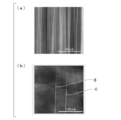
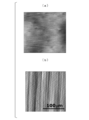
- FIG. 1 shows a normal AFM (Dimension made by Veeco Instrument).
- V shows a 10 ⁇ m square AFM image (stereoscopic surface perspective image) of the surface of the SiC epitaxial wafer.
- FIG. 1A is an AFM image showing conventional step bunching
- FIG. 1B is an AFM image showing short step bunching.
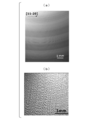
- FIG. 2 shows an AFM image of 200 ⁇ m ⁇ on the surface of the SiC epitaxial film observed by the wide-range observation type AFM (Nanoscale Hybrid Microscope VN-8000 manufactured by Keyence) used in the present invention.
- 2A is an AFM image showing conventional step bunching
- FIG. 2B is an AFM image showing short step bunching.
- FIG. 2 (a) it can be observed that the conventional step bunching exists at an average interval of about 1.5 ⁇ m as in the case of a normal AFM image.
- FIG. 2B shows that two lines (arrows B and C) are observed stably at equal intervals.
- the fact that the step can be stably observed in such a wide range of 200 ⁇ m ⁇ does not indicate mere noise or a peculiar surface area, and confirms the existence of step bunching having different properties from the conventional step bunching.
- optical surface inspection apparatus In order to confirm the presence of short step bunching with another surface inspection apparatus, observation was performed with an optical surface inspection apparatus using a laser beam (Candela CS20 manufactured by KLA-Tencor).
- This optical surface inspection apparatus is suitable for measuring the density of short step bunching because the entire surface of the wafer having a measurement range of several ⁇ m ⁇ to 4 inches ⁇ or more is larger than the wide-area observation type AFM.
- the optical surface inspection apparatus used in the present invention is a method in which laser light is incident on a wafer obliquely and scattered light from the wafer surface is reflected. It has the system which detects intensity
- the surface of the wafer is spiral scanned. Since the reflection position changes so as to trace the unevenness of the wafer surface, roughness (surface roughness) can be calculated from this position information.
- a 100 ⁇ m filter is used in the calculation, and long-period waviness information on the wafer surface is removed.
- step bunching is parallel to the [1-100] direction, a step is not detected in a region where the laser beam and the scanning direction are parallel during spiral scanning. Therefore, for the calculation of roughness information, a range of 70 ° between 55 ° to 125 ° and 235 ° to 305 ° in general polar coordinates is selected. Further, since the center of the spiral scan is a singular point where the laser beam hardly moves, the position information of the reflected light in the vicinity does not reflect the roughness. Therefore, the central ⁇ 10 mm range was excluded from the calculation area. The calculation range set in this way is about 35% of the entire wafer surface. However, with respect to step bunching, the morphology in this range almost reflects the entire wafer surface. Since the roughness calculated in this way has a correlation with the roughness measured using the AFM, it can be seen that the roughness is in accordance with the actual surface morphology.
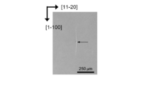
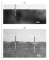
- FIG. 3 shows the observation result of the SiC epitaxial wafer in which short step bunching is observed with the optical surface inspection apparatus, using a differential interference microscope. As shown by the arrows, a noticeable shallow pit and accompanying short step bunching can be confirmed. The depth of the shallow pits on the epilayer surface was 6.3 nm.
- FIG. 4 shows an observation result by a differential interference microscope after performing KOH etching to confirm the origin of the shallow pit.
- the presence of screw dislocations and the accompanying short step bunching can be confirmed. From this, it can be inferred that the short step bunching occurred as a result of step follow growth being hindered by the step of the shallow pit generated on the surface.
- the origin of the short step bunching is the shallow pit caused by the screw dislocation in the epi layer inherited from the substrate.
- the present inventors have observed this short step bunching on the surface by observing and evaluating the surface of the SiC epitaxial film by combining an optical surface inspection device and a surface inspection device different from the conventional one called a wide-range observation type AFM. It was found that it exists as a standard state, not a unique state. As a result of intensive studies, the present inventors have clarified the origin of short step bunching and suppressed the occurrence of the step bunching, thereby reaching a method for manufacturing a step bunching-free SiC epitaxial wafer.
- the short step bunching caused by the SiC single crystal substrate was discovered. Necessary conditions were found in the polishing process of the substrate. Then, the SiC single crystal substrate polished under such conditions is subjected to gas etching to clean the SiC single crystal substrate. If this SiC single crystal substrate is used, an amount of carbon-containing gas and silicon required for epitaxial growth of silicon carbide can be obtained. It has been found that conventional step bunching and short step bunching are remarkably reduced by simultaneously forming the film by supplying the contained gas to the substrate surface at a predetermined concentration ratio. Further, the inventors have found that a step bunching-free SiC epitaxial wafer can be obtained by simultaneously stopping the supply and maintaining the substrate temperature until the gas is removed and then lowering the temperature.
- the present invention provides the following means.
- SiC epitaxial wafer characterized in that is 1 piece / cm 2 or less.
- the film thickness distribution of the SiC epitaxial layer is 2% or less and the carrier concentration distribution is 10% or less, and the main surface of the SiC epitaxial wafer warps in a convex shape at room temperature,
- the “main surface” refers to a surface on which an epitaxial film is grown on a 4H—SiC single crystal substrate.
- the “film thickness distribution” and the “carrier concentration distribution” are obtained from ⁇ (maximum value ⁇ minimum value) / (maximum value + minimum value) ⁇ ⁇ 100 (%) using samples at a plurality of locations on the wafer.
- the growth temperature for epitaxial growth of the silicon carbide film is 1600 to 1640 ° C.
- the growth rate is 1 to 3 ⁇ m / h and the growth temperature is 1640 to 1700 ° C.
- the growth rate is 3 to 4 ⁇ m / h.
- the growth temperature is 1700 to 1800 ° C.
- the growth rate is (Ii)
- the growth temperature is 1600 to 1640 ° C.
- the production method of the SiC epitaxial wafer characterized in that. “Amount required for epitaxial growth of silicon carbide” means that desorption (sublimation) and adsorption (growth) of Si and C from the substrate occur simultaneously on the surface of the substrate at an elevated temperature.
- Gas separation occurs when the separation amount is greater than the adsorption amount, and growth occurs when the desorption amount is less than the adsorption amount.
- silicon-containing gas and / or the carbon-containing gas is added during the gas etching, these raw materials are used. Since the amount of gas is small, even if the source gas is added, only preferential gas etching occurs, so the difference from the supply amount of silicon-containing gas and / or carbon-containing gas during gas etching is clarified. It is an expression made with intent.
- the silicon-containing gas and the carbon-containing gas are supplied so that the atomic ratio C / Si of carbon to silicon in an amount required for epitaxial growth of silicon carbide is 0.7 to 1.2.
- the growth temperature for epitaxially growing the silicon carbide film is set to 1600 to 1640.
- the growth temperature is set to 1 ° C. to 1 ⁇ m / h
- the growth temperature is set to 1640 to 1700 ° C.
- the growth rate is set to 3 to 4 ⁇ m / h and the growth temperature is set to 1700 to 1800 ° C.
- the growth temperature for epitaxial growth of the silicon carbide film is 1600 to 1640 ° C.
- the growth rate is 2 to 4 ⁇ m / h
- the growth temperature is 1640 to 1700 ° C.
- the growth rate is 4 to 10 ⁇ m / h.
- the 700 ⁇ 1800 ° C. performs growth rate as 10 ⁇ 20 [mu] m / h
- the production method of the SiC epitaxial wafer according to item (5) characterized in that.
- Epitaxial growth of silicon carbide film (1) When a 4H—SiC single crystal substrate with an off angle of 0.4 ° to 2 ° is used, when the growth temperature for epitaxial growth of the silicon carbide film is 1600 to 1640 ° C., When the growth rate is 1 to 3 ⁇ m / h and the growth temperature is 1640 to 1700 ° C., the growth rate is 3 to 4 ⁇ m / h. When the growth temperature is 1700 to 1800 ° C., the growth rate is 4 (2) When a 4H—SiC single crystal substrate with an off angle of 2 ° to 5 ° is used, the growth rate is 1600 to 1640 ° C. when the growth temperature for epitaxial growth of the silicon carbide film is 1600 to 1640 ° C.
- the growth rate is 4 to 10 ⁇ m / h and the growth temperature is 1700 to 1800 ° C.
- the growth rate is 4 to 10 ⁇ m / h and the growth temperature is 1700 to 1800 ° C.
- the growth rate is 10 ⁇ 20 [mu] m / h
- triangular defect density on the surface of the SiC epitaxial layer has a 1 / cm 2 or less, the density of stacking faults of SiC epitaxial wafer layer The effect that a SiC epitaxial wafer of 1 piece / cm 2 or less is obtained is obtained.
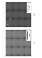
- SiC epitaxial wafer of 4 degrees off angle with the photo-luminescence imaging device (a) SiC epitaxial wafer of this invention, (b) The image which shows the conventional SiC epitaxial wafer. It is (a) image and (b) defect map which measured C surface of the SiC epitaxial wafer of the conventional 0.8 degree off angle
- SiC epitaxial wafer 5 and 6, the SiC epitaxial wafer according to the embodiment of the present invention, in which the SiC epitaxial layer is formed on the Si surface of the 4H—SiC single crystal substrate inclined at an off angle of 4 °, is observed over a wide range.
- the results of observation with an optical surface inspection apparatus (Candela CS20 manufactured by KLA-Tencor) using a type AFM and laser light are shown.
- FIG. 5 (a) is a 200 ⁇ m ⁇ wide observation type AFM image of the surface of the SiC epitaxial wafer of the present invention.
- FIG. 5 (b) shows a 200 ⁇ m ⁇ wide-range observation type AFM image of the surface of a conventional SiC epitaxial wafer.
- step linear density 0 / mm ⁇ 1
- few steps were observed for other areas of this sample. Therefore, step bunching free is realized, and it can be seen that the linear density of the step is 5 mm ⁇ 1 or less.
- the root mean square roughness Rq was 0.5 nm
- the maximum height difference Ry was 0.8 nm.
- the average Rq of three regions selected at random in the same sample was 0.41 nm, and the average Ry was 0.82 nm. Therefore, it can be seen that the observed root mean square roughness Rq is 1.0 nm or less and the maximum height difference Ry is 3.0 nm or less.
- step bunching in which a large number of steps were combined at a linear density of 340 lines / mm ⁇ 1 was observed.
- the average step line density of the other three regions of this sample was 362 lines / mm ⁇ 1 . It can also be seen that the steps extend beyond the observation range.
- the root mean square roughness Rq was 2.4 nm
- the maximum height difference Ry was 3.6 nm.
- the average Rq of three regions randomly selected from the same sample was 3.2 nm, and the average Ry was 4.5 nm.
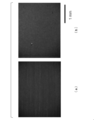
- FIGS. 6 (a) and 6 (b) are images observed by an optical surface inspection apparatus using laser light (hereinafter referred to as “candela image”) for the 1 mm ⁇ range of the same sample in FIGS. 5 (a) and 5 (b), respectively. ).
- the observed root mean square roughness Rq of the SiC epitaxial wafer of the present invention was 0.54 nm. On the other hand, it is 1.7 nm in the conventional SiC epitaxial wafer, and it can be seen that there is a clear difference in surface flatness between the present invention and the conventional SiC epitaxial wafer.
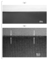
- FIG. 7A shows a photoluminescence imaging apparatus (photon design) of a SiC epitaxial wafer of the present invention in which a SiC epitaxial layer is formed on the Si surface of a 4H—SiC single crystal substrate inclined at an off angle of 4 °.
- the PL image observed with PLI-100 manufactured by the company is shown.
- FIG. 7B shows a photoluminescence imaging device (SiC epitaxial wafer) in which a SiC epitaxial wafer is formed by forming a SiC epitaxial layer on a Si surface of a 4H—SiC single crystal substrate inclined at an off angle of 4 ° by a conventional method.
- a PL image image observed with PLI-100 manufactured by Photon Design Co., Ltd. is shown.
- the stacking fault density was 0 / cm 2 .
- the stacking fault density was 2.8 / cm 2 .
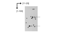
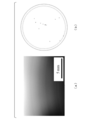
- an SiC epitaxial layer is formed on the C-plane of a 4H—SiC single crystal substrate tilted at an off angle of 0.8 °, which is an embodiment of the present invention.
- the results (candela image (a)) and defect map (b) based on the candela image of the epitaxial wafer observed with an optical surface inspection apparatus (Candela CS20 manufactured by KLA-Tencor) are shown.
- an optical surface inspection apparatus (Candela CS20 manufactured by KLA-Tencor)
- the triangular defect density is 0.4 / cm 2 (the defect density including the triangular defect is 1.2 / cm 2 ). It can be seen that it is significantly reduced as compared with the conventional SiC epitaxial wafer shown in FIG. In particular, the reduction in the peripheral region of the wafer is large. This is considered to be due to the effect of epitaxial growth using a 4H—SiC single crystal substrate whose main surface is processed into a convex shape while reducing the dent (warpage) of the substrate during epitaxial growth. It is considered that the defect density in the central part is further reduced by processing into a convex shape having an optimal curvature radius.
- FIG. 10A shows a PL image of the SiC epitaxial wafer according to the embodiment of the present invention shown in FIG. 9 observed with a photoluminescence imaging apparatus (PLI-100 manufactured by Photon Design).
- FIG. 10B is a PL image of a SiC epitaxial wafer manufactured by the conventional method shown in FIG.
- the stacking fault density was 0.1 / cm 2 .
- the SiC epitaxial wafer according to the conventional method shown in FIG. 10B three triangular light emission / absorptions are observed, and stacking faults exist.
- the stacking fault density was 1.8 / cm 2 .
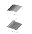
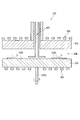
- FIG. 11 is a schematic diagram of an example of an apparatus for forming an SiC epitaxial wafer film of the present invention.
- This silicon carbide film forming apparatus 101 penetrates through a reaction chamber 104 provided between a planetary 102 and a heat radiation member 103 that supports a plurality of wafer placement portions 102b, and a central portion of the heat radiation member 103.
- the gas supply part 105 which supplies gas in the reaction chamber 104, and the high frequency coils 106 and 107 which heat the planetary 102 and the heat radiation member 103, respectively are provided.
- the revolution rotating shaft 102 a is disposed directly below the gas supply unit 105.
- the SiC single crystal wafer is revolved at a rotational speed of, for example, 5 to 20 rpm by the planetary 102 with the gas supply unit 105 as the central axis, and the SiC single crystal wafer itself is centered on the center of the SiC single crystal wafer.
- the wafer mounting unit 102b rotates at a rotational speed of 50 to 200 rpm.
- the wafer installation portion 102b and the planetary 102 are rotated by themselves to improve the in-plane uniformity of the SiC wafer thickness, carrier concentration, and temperature distribution.
- the substrate can be heated to a high temperature by the configuration in which the high-frequency coils 106 and 107 are arranged above and below the reaction chamber 104.
- the wafer mounting portion 102b is set with the growth surface (front surface) formed in a convex shape of the SiC wafer facing up.
- a temperature difference occurs between the front surface and the back surface of the SiC wafer. This is because the front surface of the substrate is cooled by the gas supplied from the gas supply unit 105.
- the substrate is warped due to a difference in thermal expansion caused by the temperature difference between the front surface and the back surface, and as a result, a part of the SiC wafer is floated from the wafer setting portion 102b, and the applied heat is generated by the SiC. Not transmitted evenly across the wafer.
- Fabrication of the SiC single crystal substrate (wafer) starts by slicing a 4H—SiC ingot manufactured by a method such as a sublimation method. Slicing is usually performed with an inner peripheral blade or a wire saw, but in recent years, a wire saw with good mass productivity is generally used. When performing convex processing, convex processing is performed in the stage of this slice.
- the amount of deflection of the wire at the time of cutting is set to 2 mm or more, and by tilting the angle formed by the plane perpendicular to the outer periphery of the cylindrical ingot with respect to the plane including the straight line formed by the wire reciprocating direction, from the ingot
- the shape of at least one surface of the SiC single crystal wafer to be cut out can be processed into a convex shape.
- the convex curvature radius is in the range of 10 m or more and 1000 m or less.
- the inclination angle is changed so that the convex direction becomes a surface used for the epitaxial surface.
- the SiC single crystal substrate processed into a convex shape is continuously and uniformly convex on the main surface.
- Continuously and uniformly convex means that there are no angular portions and a smooth state, and there are no portions that are partially concave.
- the convex curvature radius is preferably in the range of 10 m to 1000 m. This is because if it is 10 m or less, the depression of the main surface at room temperature cannot be sufficiently reduced by thermal expansion during epitaxial growth, and if it is 1000 m or more, the effect of the convex (curved) processing is not sufficient. There are several methods of measuring and quantifying the size of the convex shape (curvature, warpage).
- the curvature radius of the convex shape is measured by a wafer flatness measurement analyzer (for example, manufactured by S-Oel Corporation) It can be determined from Warp measured by UltraSort). Warp is defined as the sum of the maximum deviations in the vertical direction from the focal plane, with the focal plane as the reference plane, in a free state where the wafer is not chucked as a measurement method. Is one of the commonly used indicators.
- the Warp measurement value matches the warp value in the general definition.
- the SiC single crystal substrate may be one that satisfies either one of the main surface being curved or the SiC single crystal substrate itself being warped convexly toward the main surface.
- the main surface may be curved and the SiC single crystal substrate itself may be convexly warped.
- the 4H—SiC single crystal substrate remaining on the wafer surface in the slicing step is polished until the lattice disorder layer on the surface becomes 3 nm or less.
- the “lattice disordered layer” has a striped structure corresponding to the atomic layer (lattice) of the SiC single crystal or a part of the stripe in the TEM lattice image (image in which the lattice can be confirmed). Refers to no layer.
- FIGS. 12 and 13 show transmission electron microscope (TEM) images near the surface of the SiC single crystal substrate after the polishing step.
- FIG. 12 (a) and 12 (b) are TEM images showing examples of the SiC single crystal substrate of the present invention.
- the surface flatness disorder cannot be observed.
- FIG. 12B which is an enlarged image, disorder is observed only in the uppermost atomic layer (lattice), and a clear striped structure is observed from the lower atomic layer (lattice). it can.
- a layer sandwiched by arrows is a “lattice disorder layer”. From this TEM image, it can be confirmed that the “lattice disordered layer” on the surface is 3 nm or less.
- FIGS. 13A and 13B are TEM images showing an example of a SiC single crystal substrate having a lattice disorder layer of 3 nm or more on the surface.
- a clear disturbance of surface flatness is observed, and a lattice image (FIG. 13B) which is an enlarged image of a portion which appears flat in FIG. 13A.
- FIG. 5 the disturbance of the stripe structure can be observed over 6 nm from the surface.
- a “lattice disorder layer” of about 7 nm (a layer sandwiched between arrows on the right side in the image) can be observed, and it can be seen that the surface “lattice disorder layer” cannot achieve 3 nm or less in this sample. .
- the polishing process includes a plurality of polishing processes such as rough polishing usually called lapping, precision polishing called polishing, and chemical mechanical polishing (hereinafter referred to as CMP) which is ultra-precision polishing.
- the polishing process is often performed in a wet manner, but the common process in this process is to apply a polishing head to which a silicon carbide substrate is bonded while supplying polishing slurry to a rotating surface plate to which a polishing cloth is attached. Is to be done.
- the polishing slurry used in the present invention is basically used in such a form, but the form is not limited as long as it is wet polishing using the polishing slurry.
- the particles used as the abrasive grains may be particles that do not dissolve and disperse in this pH range.
- the pH of the polishing liquid is preferably less than 2.
- diamond, silicon carbide, aluminum oxide, titanium oxide, silicon oxide, or the like can be used as the abrasive particles.
- abrasive particles having an average diameter of 1 to 400 nm, preferably 10 to 200 nm, more preferably 10 to 150 nm are used as abrasive grains.
- silica is preferred in that small particles are commercially available at low cost. More preferred is colloidal silica.
- the particle size of an abrasive such as colloidal silica can be appropriately selected depending on processing characteristics such as processing speed and surface roughness. When a higher polishing rate is required, an abrasive having a large particle size can be used. When the surface roughness is small, that is, when a highly smooth surface is required, an abrasive having a small particle diameter can be used. Those having an average particle diameter exceeding 400 nm are expensive because they are expensive and the polishing rate is not high. When the particle diameter is extremely small such as less than 1 nm, the polishing rate is remarkably reduced.
- the addition amount of abrasive particles is 1% by mass to 30% by mass, preferably 1.5% by mass to 15% by mass. If it exceeds 30% by mass, the drying speed of the abrasive particles becomes high, which increases the risk of causing scratches, and is uneconomical. Further, if the abrasive particles are less than 1% by mass, the processing speed becomes too low, which is not preferable.
- the polishing slurry in the present invention is a water-based polishing slurry, and the pH at 20 ° C. is less than 2.0, desirably less than 1.5, and more desirably less than 1.2. In the region where the pH is 2.0 or more, a sufficient polishing rate cannot be obtained.
- the slurry less than pH 2 the chemical reactivity with respect to silicon carbide is remarkably increased even under a normal indoor environment, and ultraprecision polishing becomes possible.
- the silicon carbide is not directly removed by the mechanical action of the oxide particles in the polishing slurry, but the polishing liquid causes the silicon carbide single crystal surface to chemically react with the silicon oxide, and the silicon oxide is mechanically treated by the abrasive grains.
- polishing composition liquid so that silicon carbide can easily react, that is, setting the pH to less than 2, and selecting oxide particles having an appropriate hardness as abrasive grains can cause scratching and processing. It is very important to obtain a smooth surface without an altered layer.
- the polishing slurry is adjusted to have a pH of less than 2 using at least one acid, preferably two or more acids.
- an inorganic acid is preferable, and as the inorganic acid, hydrochloric acid, nitric acid, phosphoric acid, and sulfuric acid are preferable.
- the reason why it is effective to use a plurality of acids is unknown, but it has been confirmed by experiments, and there is a possibility that a plurality of acids interact with each other and enhance the effect.
- the amount of acid added is, for example, within the range of 0.5 to 5% by mass of sulfuric acid, 0.5 to 5% by mass of phosphoric acid, 0.5 to 5% by mass of nitric acid, and 0.5 to 5% by mass of hydrochloric acid.
- the type and amount are selected so that the pH is less than 2.
- the inorganic acid is effective because it is a stronger acid than the organic acid and is extremely convenient for adjusting to a predetermined strongly acidic polishing liquid. If an organic acid is used, it is difficult to adjust the strongly acidic polishing liquid.
- the polishing of silicon carbide is performed by removing the oxide layer with oxide particles due to the reactivity to the oxide film generated on the surface of silicon carbide by the strongly acidic polishing liquid. In order to accelerate this surface oxidation, polishing is performed.
- an oxidizing agent is added to the slurry, a further excellent effect is recognized.
- the oxidizing agent include hydrogen peroxide, perchloric acid, potassium dichromate, ammonium persulfate sulfate, and the like.
- the polishing rate is improved by adding 0.5 to 5% by mass, preferably 1.5 to 4% by mass, but the oxidizing agent is not limited to hydrogen peroxide solution. .
- an anti-gelling agent can be added to suppress gelation of the abrasive.
- phosphate ester type chelating agents such as 1-hydroxyethylidene-1,1-diphosphonic acid and aminotriethylenephosphonic acid are preferably used.
- the anti-gelling agent is added in the range of 0.01 to 6% by mass, preferably 0.05 to 2% by mass.
- the damage pressure is reduced to 50 nm by using a polishing pressure of 350 g / cm 2 or less and using abrasive grains having a diameter of 5 ⁇ m or less in mechanical polishing before CMP.
- the polishing slurry contains abrasive particles having an average particle diameter of 10 nm to 150 nm and an inorganic acid, and preferably has a pH of less than 2 at 20 ° C.
- Silica more preferably 1 to 30% by mass, and more preferably at least one of inorganic acid, hydrochloric acid, nitric acid, phosphoric acid and sulfuric acid.
- the gas etching is performed for 5 to 30 minutes while maintaining the SiC single crystal substrate at 1400 to 1800 ° C., the hydrogen gas flow rate of 40 to 120 slm, and the pressure of 100 to 250 mbar.
- the substrate After cleaning the polished SiC single crystal substrate, the substrate is set in an epitaxial growth apparatus, for example, a mass production type multiple planetary CVD apparatus. After introducing hydrogen gas into the apparatus, the pressure is adjusted to 100 to 250 mbar. Thereafter, the temperature of the apparatus is raised, the substrate temperature is set to 1400 to 1600 ° C., preferably 1480 ° C. or higher, and gas etching of the substrate surface is performed with hydrogen gas for 1 to 30 minutes. When gas etching with hydrogen gas is performed under such conditions, the etching amount is about 0.05 to 0.4 ⁇ m.
- an epitaxial growth apparatus for example, a mass production type multiple planetary CVD apparatus.
- the pressure is adjusted to 100 to 250 mbar.
- the temperature of the apparatus is raised, the substrate temperature is set to 1400 to 1600 ° C., preferably 1480 ° C. or higher, and gas etching of the substrate surface is performed with hydrogen gas for 1 to 30 minutes.
- the etching amount is about 0.05 to 0.4
- the substrate surface is damaged by the polishing process, and it is considered that not only damage that can be detected as a “lattice disorder layer” in the TEM but also distortion of the lattice that cannot be detected by the TEM exists.
- the purpose of gas etching is to remove the layer damaged in this way (hereinafter also referred to as “damage layer”).
- the gas etching is not sufficient and the damaged layer remains, dissimilar polytypes are present in the epitaxial growth layer. And dislocations and stacking faults are introduced. Further, if etching is performed too much, surface reconstruction occurs on the substrate surface, and step bunching occurs before the start of epitaxial growth. For this reason, it is important to optimize the damaged layer and the amount of gas etching.
- the present inventors have found that as a sufficient condition in the production of a step bunching-free SiC epitaxial wafer, They found a combination of the damage layer when the layer was thinned to 3 nm or less and the gas etching conditions described above.
- the root mean square roughness Rq of the outermost surface of the epitaxial layer obtained by analyzing an area of 35% or more of the entire wafer surface using an optical surface inspection apparatus is 1.3 nm or less. I can confirm that.
- the step bunching is 1.0 nm or less at 10 ⁇ m ⁇ , 1.0 nm or less at 200 ⁇ m ⁇ , and a length of 100 to 500 ⁇ m observed at 200 ⁇ m ⁇ . It can be confirmed that the maximum height difference Ry in (short step bunching) is 3.0 nm or less. It can also be confirmed that the linear density of this step is 5 mm ⁇ 1 or less. It is important to maintain the flatness of the substrate surface in the subsequent film forming process and temperature lowering process.
- SiH 4 gas and / or C 3 H 8 gas may be added to the hydrogen gas.
- SiH 4 gas having a concentration of less than 0.009 mol% is added to hydrogen gas to make the environment in the reactor Si-rich.
- the depth of the shallow pit can be reduced, and the occurrence of short step bunching associated with the shallow pit can be suppressed.
- SiH 4 gas and / or C 3 H 8 gas it is preferable to evacuate once to form a hydrogen gas atmosphere before the film formation (epitaxial growth) step.
- ⁇ Film formation (epitaxial growth) process In the film formation (epitaxial growth) step (after the temperature rise when the growth temperature of the epitaxial film is higher than the cleaning (gas etching) temperature), it is required for the epitaxial growth of silicon carbide on the surface of the cleaned substrate.
- a quantity of SiH 4 gas and C 3 H 8 gas are simultaneously supplied at a concentration ratio C / Si of 0.7 to 1.2 to epitaxially grow silicon carbide.
- “simultaneous supply” means that supply is not required until the time is completely the same, but is supplied with a difference within several seconds.
- Hot Wall SiC CVD VP2400HW
- step bunching-free SiC epitaxial wafer could be manufactured.
- Each flow rate, pressure, substrate temperature, and growth temperature of SiH 4 gas and C 3 H 8 gas are 15 to 150 sccm, 3.5 to 60 sccm, 80 to 250 mbar, higher than 1600 ° C. and lower than 1800 ° C., and the growth rate is 1 hour / hour. It is determined within the range of ⁇ 20 ⁇ m while controlling the off angle, film thickness, carrier concentration uniformity, and growth rate.
- the carrier concentration in the epitaxial layer can be controlled.
- the epitaxial layer to be grown usually has a film thickness of about 5 to 20 ⁇ m and a carrier concentration of about 2 to 15 ⁇ 10 15 cm ⁇ 3 .
- the growth temperature and growth rate depend on the off angle of the SiC single crystal substrate.
- the growth is performed by epitaxially growing a silicon carbide film.
- the temperature is 1600 to 1640 ° C.
- the growth rate is 1 to 3 ⁇ m / h.
- the growth temperature is 1640 to 1700 ° C.
- the growth rate is 3 to 4 ⁇ m / h
- the growth temperature is 1700 to 1700 ° C.
- the growth rate is 4 to 10 ⁇ m / h.
- the growth temperature for epitaxial growth of the silicon carbide film is set.
- the growth rate is 1600 to 1640 ° C.
- the growth rate is 2 to 4 ⁇ m / h.
- the growth temperature is 1640 to 1700 ° C.
- the growth rate is 4 to 10 ⁇ m / h.
- the degrees and 1700 ⁇ 1800 ° C. performs growth rate as 10 ⁇ 20 ⁇ m / h.
- the supply of SiH 4 gas and C 3 H 8 gas and the introduction of nitrogen gas as a doping gas are stopped and the temperature is lowered.
- gas etching occurs on the surface of the SiC epitaxial film, deteriorating the surface morphology. obtain.
- the timing of stopping the supply of the SiH 4 gas and the C 3 H 8 gas and the timing of temperature decrease are important. By simultaneously stopping the supply of SiH 4 gas and C 3 H 8 gas, holding the growth temperature until these supplied gases disappear from the substrate surface, and then lowering the temperature to room temperature at an average rate of about 50 ° C. It was found that deterioration of morphology was suppressed.
- SiH 4 gas as a silicon-containing gas and C 3 H 8 gas as a carbon-containing gas, N 2 gas as a doping gas, H 2 gas as a carrier gas and an etching gas are used, and a mass production type multiple-planetary is used.
- Example 1 A SiC epitaxial layer is formed on the Si surface of a 4H—SiC single crystal substrate inclined at an off angle of 4 °.
- the 4H—SiC single crystal substrate is not subjected to convex processing.
- mechanical polishing before CMP was performed at a processing pressure of 350 g / cm 2 using abrasive grains having a diameter of 5 ⁇ m or less.
- CMP was performed for 30 minutes using silica particles having an average particle diameter of 10 to 150 nm as abrasive particles, a slurry containing sulfuric acid as an inorganic acid and a pH of 1.9 at 20 ° C. Thereby, the lattice disorder layer on the surface was made 3 nm or less.
- the polished substrate was introduced into the growth apparatus after RCA cleaning.
- the RCA cleaning is a wet cleaning method generally used for Si wafers, and a substrate is prepared by using a mixed solution of sulfuric acid / ammonia / hydrochloric acid and hydrogen peroxide solution and a hydrofluoric acid aqueous solution. Organic substances, heavy metals and particles on the surface can be removed.
- the cleaning (gas etching) step was performed at a hydrogen gas flow rate of 100 slm, a reactor internal pressure of 200 mbar, and a substrate temperature of 1500 ° C. for 20 minutes.
- the substrate temperature is set to 1650 ° C.
- C 3 H 8 gas 24 sccm and SiH 4 gas 8 sccm are simultaneously started so that SiH 4 gas and C 3 H 8 gas are simultaneously supplied to the main surface of the substrate. went.
- C / Si was selected to be 1.0.
- a SiC epitaxial layer having a thickness of 10 ⁇ m was formed by carrying out a growth process for 2 hours at a growth rate of 5 ⁇ m / h with the pressure in the reactor set to 200 mbar.
- a wide-area observation type AFM Keyence Nanoscale Hybrid Microscope VN-8000
- an optical surface inspection device KLA-Tencor Candela CS20
- a photoluminescence imaging device Photon Design
- Rq measured by the optical surface inspection apparatus was 1.2 nm
- Rq measured by the wide-range observation type AFM was 0.4 nm
- the maximum height difference Ry was 0.6 nm
- step bunching was not observed.
- the density of triangular defects on the surface of the epitaxial film of the SiC epitaxial wafer was 0.6 / cm 2
- the density of stacking faults in the film of the epitaxial film of the SiC epitaxial wafer was 0 / cm 2 .
- the production conditions of the SiC epitaxial wafer are the same as those in Example 1 except that the substrate growth temperature is 1600 ° C.
- the SiC epitaxial wafer thus manufactured was measured with an optical surface inspection device (Candela CS20 manufactured by KLA-Tencor) and a photoluminescence imaging device (PLI-100 manufactured by Photon Design).
- an optical surface inspection device Candela CS20 manufactured by KLA-Tencor
- a photoluminescence imaging device PLI-100 manufactured by Photon Design
- triangular defects on the surface of the SiC epitaxial wafer were measured.
- the density was 2.4 / cm 2 , and triangular defects were present throughout the wafer.
- the stacking fault density in the film of the SiC epitaxial wafer is 2.8 / cm 2, which is considerably larger than that of the first embodiment of the present invention. From this comparison, it was found that there is a growth temperature that reduces the defect density at a temperature higher than the upper limit (1600 ° C.) of the
- Example 2 [Si surface of 4H-SiC single crystal substrate with an off angle of 1.2 °] (Example 2)
- a SiC epitaxial wafer was fabricated under the same fabrication conditions as in Example 1 except that the growth process was performed at a growth rate of 4 ⁇ m / h for 2.5 hours.
- an optical surface inspection apparatus (Candela CS20 manufactured by KLA-Tencor), a photoluminescence imaging apparatus (PLI-100 manufactured by Photon Design), and a wide-range observation type AFM (Nanoscale hybrid microscope manufactured by Keyence) VN-8000).
- the triangular defect density was 0.4 / cm 2
- the stacking fault density was 0.1 / cm 2 . Step bunching was not observed. All of them were 1 piece / cm 2 or less, and an extremely high quality epitaxial film having a low defect density was formed on a 4H—SiC single crystal substrate having an off angle of 1.2 °, which is lower than that of Example 1.
- Example 3 [C-plane of 4H-SiC single crystal substrate with off angle of 0.8 °] (Example 3)
- Example 1 except that the Si surface was sliced into a convex shape using a multi-wire saw so that the convex curvature radius was 50 m, and the growth step was performed at a growth rate of 4 ⁇ m / h for 2.5 hours.
- a SiC epitaxial wafer was produced under the same production conditions. With respect to the manufactured SiC epitaxial wafer, the results of measurement with an optical surface inspection apparatus (Candela CS20 manufactured by KLA-Tencor) and photoluminescence imaging apparatus (PLI-100 manufactured by Photon Design) are as shown in FIG. It is.
- an optical surface inspection apparatus Candela CS20 manufactured by KLA-Tencor
- PLI-100 photoluminescence imaging apparatus manufactured by Photon Design
- the triangular defect density was 0.4 / cm 2
- the stacking fault density was 0.2 / cm 2
- an extremely high quality epitaxial film having a defect density of 1 piece / cm 2 or less and having a low defect density was formed on the Si surface of the 4H—SiC single crystal substrate having a low off-angle.
- step bunching was not observed in the measurement using the optical surface inspection apparatus (Candela CS20 manufactured by KLA-Tencor) and the wide-area observation type AFM (Nanoscale hybrid microscope VN-8000 manufactured by Keyence).
- a mercury probe concentration analyzer (Hg-CV) (495 CV SYSTEM manufactured by SSSM) was used, and for the carrier concentration uniformity, a fast Fourier transform infrared absorption analyzer (FT-IR) (QS1200 manufactured by Nanometrics). ).
- the film thickness uniformity was 2%, the carrier concentration uniformity was 8%, and a SiC epitaxial layer with good in-plane uniformity was formed.
- “Film thickness distribution” and “carrier concentration distribution” were obtained from ⁇ (maximum value ⁇ minimum value) / (maximum value + minimum value) ⁇ ⁇ 100 (%) using eight samples on the wafer. is there.
- the film thickness uniformity is about 5 to 10%, and the carrier concentration uniformity is about 15 to 20%. Improved uniformity.
- Example 2 The production conditions of the SiC epitaxial wafer are the same as those in Example 3 except that the substrate growth temperature is 1600 ° C.
- the SiC epitaxial wafer thus produced was measured with an optical surface inspection apparatus (Candela CS20 manufactured by KLA-Tencor) and a photoluminescence imaging apparatus (PLI-100 manufactured by Photon Design). The results are shown in FIGS.
- the density of triangular defects on the surface of the SiC epitaxial wafer was 4 / cm 2 , and there were triangular defects throughout the wafer.
- the stacking fault density in the film of the SiC epitaxial wafer is 1.8 / cm 2, which is considerably higher than that of Example 3 of the present invention. From this comparison, it was found that there is a growth temperature that reduces the defect density at a temperature higher than the upper limit (1600 ° C.) of the conventional growth temperature.
- An SiC epitaxial film was grown on a Si surface inclined by 4 ° in the ⁇ 11-20> axis direction with respect to the (0001) plane of the 4H—SiC single crystal by Hot Wall SiC CVD (VP2400HW).
- an optical surface inspection apparatus (Candela CS20 manufactured by KLA-Tencor), a normal AFM (Dimension V manufactured by Veeco Instrument) and a wide-area observation type AFM (Nanoscale hybrid microscope manufactured by Keyence) VN-8000).
- Example 1 The polishing step and subsequent cleaning were performed under the same conditions as in Example 1.
- the cleaning (gas etching) step was carried out at a hydrogen gas flow rate of 90 slm, a reactor pressure of 200 mbar, and a substrate temperature of 1550 ° C. for 10 minutes.
- SiH 4 gas is supplied after 3 seconds. did. C / Si selected 1.1.
- a growth process was performed for 2 hours at a growth rate of 5 ⁇ m / h with a reactor internal pressure of 200 mbar and a substrate temperature of 1550 ° C., thereby forming a 10 ⁇ m thick SiC epitaxial layer.
- the Rq measured with the wide-area observation type AFM and the optical surface inspection apparatus was 1.2 nm, and the Rq measured with the wide-area observation type AFM was Rq. It was 0.4 nm, the maximum height difference Ry was 0.7 nm, and no step bunching was observed.
- Sample 2 A SiC epitaxial wafer was manufactured under the same conditions as in Sample 1 except for gas etching conditions.
- the gas etching step is different from Sample 1 in that SiH 4 gas having a concentration of 0.008 mol% is added to hydrogen gas.
- the SiC epitaxial wafer thus produced was measured with an optical surface inspection apparatus and a wide-area observation type AFM.
- An image similar to Sample 1 was observed, Rq measured with an optical surface inspection apparatus was 1.1 nm, Rq measured with a wide-range observation type AFM was 0.4 nm, and the maximum height difference Ry was 0.7 nm. .
- FIGS. 6B and 5B Images of the manufactured SiC epitaxial wafer measured by an optical surface inspection apparatus and a wide-area observation type AFM are as shown in FIGS. 6B and 5B, respectively.
- the root mean square roughness Rq measured by the optical surface inspection apparatus was 1.7 nm
- the root mean square roughness Rq measured by the wide-range observation type AFM was 2.4 nm
- the maximum height difference Ry was 3.6 nm. .
- FIGS. 14A and 14B show a candela image and a wide-range observation type AFM image for the manufactured SiC epitaxial wafer.
- the root mean square roughness Rq measured by the optical surface inspection apparatus was 1.4 nm
- the root mean square roughness Rq measured by the wide range observation type AFM was 1.4 nm
- the maximum height difference Ry was 2.8 nm.
- the linear density of the step was 10 pieces / mm ⁇ 1 .
- the SiC epitaxial wafer of the present invention is a step-bunching-free SiC epitaxial wafer in which triangular defects and stacking faults are reduced, the carrier concentration and film thickness are high, and various devices such as power devices, high-frequency devices, and high-temperature operation devices. It can be used for the manufacture of a silicon carbide semiconductor device.
Landscapes
- Chemical & Material Sciences (AREA)
- Engineering & Computer Science (AREA)
- Materials Engineering (AREA)
- Crystallography & Structural Chemistry (AREA)
- Metallurgy (AREA)
- Organic Chemistry (AREA)
- Manufacturing & Machinery (AREA)
- Physics & Mathematics (AREA)
- Condensed Matter Physics & Semiconductors (AREA)
- General Physics & Mathematics (AREA)
- Computer Hardware Design (AREA)
- Microelectronics & Electronic Packaging (AREA)
- Power Engineering (AREA)
- General Chemical & Material Sciences (AREA)
- Chemical Kinetics & Catalysis (AREA)
- Inorganic Chemistry (AREA)
- Mechanical Engineering (AREA)
- Crystals, And After-Treatments Of Crystals (AREA)
- Chemical Vapour Deposition (AREA)
Priority Applications (4)
| Application Number | Priority Date | Filing Date | Title |
|---|---|---|---|
| EP10837482.8A EP2514857B1 (en) | 2009-12-14 | 2010-12-08 | SiC EPITAXIAL WAFER AND METHOD FOR MANUFACTURING SAME |
| KR1020127017058A KR101377813B1 (ko) | 2009-12-14 | 2010-12-08 | SiC 에피택셜 웨이퍼 및 그 제조 방법 |
| US13/515,443 US20120280254A1 (en) | 2009-12-14 | 2010-12-08 | Sic epitaxial wafer and method for manufacturing same |
| CN201080056408.0A CN102656297B (zh) | 2009-12-14 | 2010-12-08 | SiC外延晶片及其制造方法 |
Applications Claiming Priority (2)
| Application Number | Priority Date | Filing Date | Title |
|---|---|---|---|
| JP2009-283113 | 2009-12-14 | ||
| JP2009283113A JP4887418B2 (ja) | 2009-12-14 | 2009-12-14 | SiCエピタキシャルウェハの製造方法 |
Publications (1)
| Publication Number | Publication Date |
|---|---|
| WO2011074453A1 true WO2011074453A1 (ja) | 2011-06-23 |
Family
ID=44167210
Family Applications (1)
| Application Number | Title | Priority Date | Filing Date |
|---|---|---|---|
| PCT/JP2010/071989 WO2011074453A1 (ja) | 2009-12-14 | 2010-12-08 | SiCエピタキシャルウェハ及びその製造方法 |
Country Status (6)
Cited By (22)
| Publication number | Priority date | Publication date | Assignee | Title |
|---|---|---|---|---|
| WO2013161022A1 (ja) * | 2012-04-25 | 2013-10-31 | 株式会社エコトロン | 炭化珪素半導体薄膜の形成方法および炭化珪素半導体基板 |
| CN103649385A (zh) * | 2011-07-19 | 2014-03-19 | 昭和电工株式会社 | SiC外延晶片及其制造方法、以及SiC外延晶片的制造装置 |
| US20140193965A1 (en) * | 2009-08-20 | 2014-07-10 | The Government Of The United States Of America, As Represented By The Secretary Of The Navy | REDUCTION OF BASAL PLANE DISLOCATIONS IN EPITAXIAL SiC USING AN IN-SITU ETCH PROCESS |
| CN104428872A (zh) * | 2012-05-30 | 2015-03-18 | Lg伊诺特有限公司 | 碳化硅外延晶片及其制造方法 |
| EP2755228A4 (en) * | 2011-09-09 | 2015-04-15 | Showa Denko Kk | EPITACTIC SILICON CARBIDE WAFERS AND METHOD OF MANUFACTURING THEREOF |
| JP2015529015A (ja) * | 2013-03-15 | 2015-10-01 | ダウ コーニング コーポレーションDow Corning Corporation | SiCエピタキシャル膜を有するSiC基板 |
| WO2016051975A1 (ja) * | 2014-10-01 | 2016-04-07 | 住友電気工業株式会社 | 炭化珪素エピタキシャル基板 |
| US9337277B2 (en) | 2012-09-11 | 2016-05-10 | Dow Corning Corporation | High voltage power semiconductor device on SiC |
| JP2016149566A (ja) * | 2014-08-29 | 2016-08-18 | 住友電気工業株式会社 | 炭化珪素半導体装置およびその製造方法 |
| WO2017043164A1 (ja) * | 2015-09-11 | 2017-03-16 | 住友電気工業株式会社 | 炭化珪素エピタキシャル基板および炭化珪素半導体装置の製造方法 |
| US20170233893A1 (en) * | 2012-06-19 | 2017-08-17 | Showa Denko K.K. | Sic epitaxial wafer and method for manufacturing the same |
| US9738991B2 (en) | 2013-02-05 | 2017-08-22 | Dow Corning Corporation | Method for growing a SiC crystal by vapor deposition onto a seed crystal provided on a supporting shelf which permits thermal expansion |
| JP2017145150A (ja) * | 2016-02-15 | 2017-08-24 | 住友電気工業株式会社 | 炭化珪素エピタキシャル基板および炭化珪素半導体装置の製造方法 |
| US9797064B2 (en) | 2013-02-05 | 2017-10-24 | Dow Corning Corporation | Method for growing a SiC crystal by vapor deposition onto a seed crystal provided on a support shelf which permits thermal expansion |
| US10002760B2 (en) | 2014-07-29 | 2018-06-19 | Dow Silicones Corporation | Method for manufacturing SiC wafer fit for integration with power device manufacturing technology |
| WO2018142744A1 (ja) * | 2017-01-31 | 2018-08-09 | 住友電気工業株式会社 | 炭化珪素エピタキシャル基板および炭化珪素半導体装置の製造方法 |
| WO2019043973A1 (ja) * | 2017-09-01 | 2019-03-07 | 住友電気工業株式会社 | 炭化珪素エピタキシャル基板 |
| US10612160B2 (en) | 2014-08-01 | 2020-04-07 | Sumitomo Electric Industries, Ltd. | Epitaxial wafer and method for manufacturing same |
| JP2020090436A (ja) * | 2019-12-24 | 2020-06-11 | 住友電気工業株式会社 | 炭化珪素エピタキシャル基板および炭化珪素半導体装置の製造方法 |
| JP2020114796A (ja) * | 2016-02-15 | 2020-07-30 | 住友電気工業株式会社 | 炭化珪素エピタキシャル基板および炭化珪素半導体装置の製造方法 |
| JP2021020853A (ja) * | 2019-12-24 | 2021-02-18 | 住友電気工業株式会社 | 炭化珪素エピタキシャル基板および炭化珪素半導体装置の製造方法 |
| JPWO2020017208A1 (ja) * | 2018-07-20 | 2021-07-15 | 住友電気工業株式会社 | 炭化珪素エピタキシャル基板および炭化珪素半導体装置の製造方法 |
Families Citing this family (80)
| Publication number | Priority date | Publication date | Assignee | Title |
|---|---|---|---|---|
| US10256090B2 (en) * | 2009-08-20 | 2019-04-09 | The United States Of America, As Represented By The Secretary Of The Navy | Reduction of basal plane dislocations in epitaxial SiC using an in-situ etch process |
| US9464366B2 (en) | 2009-08-20 | 2016-10-11 | The United States Of America, As Represented By The Secretary Of The Navy | Reduction of basal plane dislocations in epitaxial SiC |
| KR101454978B1 (ko) * | 2009-08-27 | 2014-10-27 | 신닛테츠스미킨 카부시키카이샤 | SiC 단결정 웨이퍼와 그 제조 방법 |
| CN103370454B (zh) * | 2011-04-21 | 2015-09-09 | 新日铁住金株式会社 | 外延碳化硅单晶基板及其制造方法 |
| US20130062628A1 (en) * | 2011-09-10 | 2013-03-14 | Semisouth Laboratories, Inc. | Methods for the epitaxial growth of silicon carbide |
| JP5853648B2 (ja) | 2011-11-30 | 2016-02-09 | 住友電気工業株式会社 | 炭化珪素半導体装置の製造方法 |
| KR101942514B1 (ko) * | 2011-12-16 | 2019-01-28 | 엘지이노텍 주식회사 | 탄화규소 증착 방법 및 탄화규소 에피 웨이퍼 |
| KR101936171B1 (ko) * | 2011-12-19 | 2019-04-04 | 엘지이노텍 주식회사 | 탄화규소 에피 웨이퍼 제조 방법 및 탄화규소 에피 웨이퍼 |
| KR101942536B1 (ko) * | 2011-12-19 | 2019-01-29 | 엘지이노텍 주식회사 | 탄화규소 에피 웨이퍼 제조 방법 |
| KR101936170B1 (ko) * | 2011-12-19 | 2019-01-08 | 엘지이노텍 주식회사 | 탄화규소 에피 웨이퍼 제조 방법 |
| KR101926678B1 (ko) * | 2012-05-31 | 2018-12-11 | 엘지이노텍 주식회사 | 탄화규소 에피 웨이퍼 및 이의 제조 방법 |
| US9018639B2 (en) | 2012-10-26 | 2015-04-28 | Dow Corning Corporation | Flat SiC semiconductor substrate |
| TW201417150A (zh) * | 2012-10-31 | 2014-05-01 | Lg Innotek Co Ltd | 磊晶晶圓 |
| TW201417149A (zh) * | 2012-10-31 | 2014-05-01 | Lg Innotek Co Ltd | 磊晶晶圓 |
| KR102098209B1 (ko) * | 2013-02-05 | 2020-04-08 | 엘지이노텍 주식회사 | 에피택셜 웨이퍼 및 그 제조 방법 |
| CN104937699B (zh) * | 2012-11-30 | 2018-12-18 | Lg 伊诺特有限公司 | 外延晶片和使用其的开关元件及发光元件 |
| KR102053077B1 (ko) * | 2012-11-30 | 2020-01-08 | 엘지이노텍 주식회사 | 에피택셜 웨이퍼 및 그 제조 방법 |
| KR102119755B1 (ko) * | 2012-11-30 | 2020-06-08 | 엘지이노텍 주식회사 | 에피택셜 웨이퍼 및 그 제조 방법 |
| US9017804B2 (en) | 2013-02-05 | 2015-04-28 | Dow Corning Corporation | Method to reduce dislocations in SiC crystal growth |
| JP6012841B2 (ja) * | 2013-02-13 | 2016-10-25 | 三菱電機株式会社 | SiCエピタキシャルウエハの製造方法 |
| CN103199008A (zh) * | 2013-03-11 | 2013-07-10 | 西安电子科技大学 | 零偏4H-SiC衬底上的同质外延方法 |
| JP6123408B2 (ja) | 2013-03-26 | 2017-05-10 | 三菱電機株式会社 | 単結晶4H−SiC基板及びその製造方法 |
| JP6112712B2 (ja) * | 2013-03-27 | 2017-04-12 | 国立研究開発法人産業技術総合研究所 | 炭化珪素エピタキシャルウエハの製造方法 |
| JP2014189442A (ja) | 2013-03-27 | 2014-10-06 | Sumitomo Electric Ind Ltd | 炭化珪素半導体基板の製造方法 |
| JP2014210690A (ja) * | 2013-04-22 | 2014-11-13 | 住友電気工業株式会社 | 炭化珪素基板の製造方法 |
| JP6136731B2 (ja) * | 2013-08-06 | 2017-05-31 | 住友電気工業株式会社 | 炭化珪素半導体基板およびその製造方法、ならびに炭化珪素半導体装置の製造方法 |
| JP6386706B2 (ja) * | 2013-09-06 | 2018-09-05 | 住友電気工業株式会社 | 炭化珪素エピタキシャル基板、炭化珪素エピタキシャル基板の製造方法、炭化珪素半導体装置の製造方法、炭化珪素成長装置および炭化珪素成長装置用部材 |
| JP6172672B2 (ja) * | 2013-10-11 | 2017-08-02 | 大陽日酸株式会社 | 気相成長装置の膜厚測定方法 |
| CN103820768A (zh) * | 2014-03-11 | 2014-05-28 | 中国科学院半导体研究所 | 4H-SiC衬底上同质快速外延生长4H-SiC外延层的方法 |
| JP6311384B2 (ja) | 2014-03-24 | 2018-04-18 | 三菱電機株式会社 | 炭化珪素半導体装置の製造方法 |
| CN106233430B (zh) * | 2014-04-18 | 2019-08-06 | 国立研究开发法人产业技术综合研究所 | 碳化硅外延晶片及其制造方法 |
| JP6479347B2 (ja) * | 2014-06-06 | 2019-03-06 | ローム株式会社 | SiCエピタキシャルウェハの製造装置、およびSiCエピタキシャルウェハの製造方法 |
| JP6259740B2 (ja) * | 2014-09-11 | 2018-01-10 | 国立大学法人名古屋大学 | 炭化ケイ素の結晶の製造方法及び結晶製造装置 |
| US9777404B2 (en) * | 2014-11-12 | 2017-10-03 | Sumitomo Electric Industries, Ltd. | Method for manufacturing silicon carbide epitaxial substrate, and silicon carbide epitaxial substrate |
| JP2016127201A (ja) * | 2015-01-07 | 2016-07-11 | 三菱電機株式会社 | 炭化珪素エピタキシャル基板の製造方法および炭化珪素半導体装置の製造方法 |
| JP2016132604A (ja) * | 2015-01-21 | 2016-07-25 | 住友電気工業株式会社 | 炭化珪素基板および炭化珪素基板の製造方法 |
| CN107208311B (zh) * | 2015-02-18 | 2019-12-10 | 昭和电工株式会社 | 碳化硅单晶块的制造方法和碳化硅单晶块 |
| US10727047B2 (en) | 2015-02-18 | 2020-07-28 | Showa Denko K.K. | Epitaxial silicon carbide single crystal wafer and process for producing the same |
| KR102044616B1 (ko) * | 2015-03-03 | 2019-11-13 | 쇼와 덴코 가부시키가이샤 | SiC 에피택셜 웨이퍼, SiC 에피택셜 웨이퍼의 제조 방법 |
| CN105006425A (zh) * | 2015-06-08 | 2015-10-28 | 国网智能电网研究院 | 一种无台阶聚集低偏角碳化硅外延生长方法 |
| EP3330415B1 (en) * | 2015-07-29 | 2025-03-12 | Resonac Corporation | Method for producing epitaxial silicon carbide single-crystal wafer |
| JP6447732B2 (ja) * | 2015-07-30 | 2019-01-09 | 富士電機株式会社 | SiC基板の製造方法 |
| JP6544166B2 (ja) * | 2015-09-14 | 2019-07-17 | 信越化学工業株式会社 | SiC複合基板の製造方法 |
| JP6584253B2 (ja) * | 2015-09-16 | 2019-10-02 | ローム株式会社 | SiCエピタキシャルウェハ、SiCエピタキシャルウェハの製造装置、SiCエピタキシャルウェハの製造方法、および半導体装置 |
| JP6573514B2 (ja) * | 2015-09-17 | 2019-09-11 | 昭和電工株式会社 | SiC単結晶基板の前処理方法及びエピタキシャルSiCウェハの製造方法 |
| US20170275779A1 (en) * | 2015-10-07 | 2017-09-28 | Sumitomo Electric Industries, Ltd. | Silicon carbide epitaxial substrate and method for manufacturing silicon carbide semiconductor device |
| CN105826186B (zh) * | 2015-11-12 | 2018-07-10 | 中国电子科技集团公司第五十五研究所 | 高表面质量碳化硅外延层的生长方法 |
| JP6069545B2 (ja) * | 2016-01-20 | 2017-02-01 | 昭和電工株式会社 | SiCエピタキシャルウェハの評価方法 |
| JP6493690B2 (ja) * | 2016-08-31 | 2019-04-03 | 昭和電工株式会社 | SiCエピタキシャルウェハ及びその製造方法、並びに、ラージピット欠陥検出方法、欠陥識別方法 |
| US11293115B2 (en) | 2016-08-31 | 2022-04-05 | Showa Denko K.K. | Method for producing a SiC epitaxial wafer containing a total density of large pit defects and triangular defects of 0.01 defects/cm2 or more and 0.6 defects/cm2 or less |
| WO2018043169A1 (ja) * | 2016-08-31 | 2018-03-08 | 昭和電工株式会社 | SiCエピタキシャルウェハ及びその製造方法、並びに、ラージピット欠陥検出方法、欠陥識別方法 |
| JP6459132B2 (ja) * | 2016-08-31 | 2019-01-30 | 昭和電工株式会社 | SiCエピタキシャルウェハ及びその製造方法、並びに、欠陥識別方法 |
| US20200043725A1 (en) * | 2016-10-28 | 2020-02-06 | Sumitomo Electric Industries, Ltd. | Method for manufacturing a silicon carbide epitaxial substrate |
| JP6748572B2 (ja) * | 2016-12-28 | 2020-09-02 | 昭和電工株式会社 | p型SiCエピタキシャルウェハ及びその製造方法 |
| JP6762484B2 (ja) * | 2017-01-10 | 2020-09-30 | 昭和電工株式会社 | SiCエピタキシャルウェハ及びその製造方法 |
| JP6930640B2 (ja) * | 2017-03-08 | 2021-09-01 | 住友電気工業株式会社 | 炭化珪素単結晶基板、炭化珪素エピタキシャル基板および炭化珪素半導体装置の製造方法 |
| JP6824088B2 (ja) * | 2017-03-24 | 2021-02-03 | 昭和電工株式会社 | 炭化珪素のエピタキシャル成長方法 |
| US10950435B2 (en) * | 2017-04-06 | 2021-03-16 | Mitsubishi Electric Corporation | SiC epitaxial wafer, method for manufacturing SiC epitaxial wafer, SiC device, and power conversion apparatus |
| WO2018211737A1 (ja) * | 2017-05-17 | 2018-11-22 | 三菱電機株式会社 | SiCエピタキシャルウエハおよびその製造方法 |
| JP7002932B2 (ja) * | 2017-12-22 | 2022-01-20 | 昭和電工株式会社 | SiCインゴットの製造方法 |
| JP2018067736A (ja) * | 2018-01-16 | 2018-04-26 | 三菱電機株式会社 | 炭化珪素半導体装置及びその製造方法 |
| CN112136203B (zh) * | 2018-05-23 | 2024-04-09 | 三菱电机株式会社 | SiC外延基板的制造方法 |
| JP7447392B2 (ja) * | 2018-09-10 | 2024-03-12 | 株式会社レゾナック | SiC基板の評価方法及びSiCエピタキシャルウェハの製造方法 |
| JP6585799B1 (ja) * | 2018-10-15 | 2019-10-02 | 昭和電工株式会社 | SiC基板の評価方法及びSiCエピタキシャルウェハの製造方法 |
| JP7217608B2 (ja) * | 2018-10-16 | 2023-02-03 | 昭和電工株式会社 | SiC基板、SiCエピタキシャルウェハ及びその製造方法 |
| JP7063259B2 (ja) * | 2018-12-27 | 2022-05-09 | 株式会社Sumco | シリコンエピタキシャルウェーハの製造方法 |
| JP7148427B2 (ja) | 2019-02-06 | 2022-10-05 | 昭和電工株式会社 | SiCエピタキシャルウェハ及びその製造方法 |
| JP7046026B2 (ja) * | 2019-03-01 | 2022-04-01 | 三菱電機株式会社 | SiCエピタキシャルウエハ、半導体装置、電力変換装置 |
| JP2020170816A (ja) * | 2019-04-05 | 2020-10-15 | 三菱電機株式会社 | 炭化珪素エピタキシャルウエハ、炭化珪素エピタキシャルウエハの製造方法、電力変換装置 |
| RU2716866C1 (ru) * | 2019-06-06 | 2020-03-17 | Публичное Акционерное Общество "Электровыпрямитель" | Способ роста эпитаксиальных слоев карбида кремния р-типа проводимости с малой плотностью базальных дислокаций |
| CN110281142A (zh) * | 2019-06-20 | 2019-09-27 | 山东大学 | 金刚石籽晶制备方法、金刚石籽晶及单晶 |
| CN113122147B (zh) * | 2019-12-31 | 2024-03-12 | 安集微电子科技(上海)股份有限公司 | 一种化学机械抛光液及其使用方法 |
| KR102229588B1 (ko) | 2020-05-29 | 2021-03-17 | 에스케이씨 주식회사 | 웨이퍼의 제조방법, 에피택셜 웨이퍼의 제조방법, 이에 따라 제조된 웨이퍼 및 에피택셜 웨이퍼 |
| JP7610934B2 (ja) * | 2020-07-21 | 2025-01-09 | 三菱電機株式会社 | 炭化珪素エピタキシャルウエハの製造方法 |
| CN112259451B (zh) * | 2020-09-22 | 2022-11-29 | 山东天岳先进科技股份有限公司 | 一种碳化硅晶片的位错识别方法及碳化硅晶片与应用 |
| KR102283879B1 (ko) | 2021-01-14 | 2021-07-29 | 에스케이씨 주식회사 | 탄화규소 웨이퍼의 제조방법, 탄화규소 웨이퍼 및 웨이퍼 제조용 시스템 |
| KR102321229B1 (ko) | 2021-03-30 | 2021-11-03 | 주식회사 쎄닉 | 탄화규소 웨이퍼 및 이를 적용한 반도체 소자 |
| CN113594027A (zh) * | 2021-07-27 | 2021-11-02 | 兰州大学 | 一种腐蚀4h-碳化硅表面的方法 |
| JP7183358B1 (ja) * | 2021-08-04 | 2022-12-05 | 昭和電工株式会社 | SiCエピタキシャルウェハ及びSiCエピタキシャルウェハの製造方法 |
| JP7285890B2 (ja) | 2021-08-04 | 2023-06-02 | 株式会社レゾナック | SiCエピタキシャルウェハ及びSiCエピタキシャルウェハの製造方法 |
Citations (6)
| Publication number | Priority date | Publication date | Assignee | Title |
|---|---|---|---|---|
| JP2005277229A (ja) | 2004-03-25 | 2005-10-06 | National Institute Of Advanced Industrial & Technology | 炭化珪素平滑化基板の作製方法、炭化珪素平滑化基板、炭化珪素エピタキシャルウエハ、窒化ガリウムウエハ、及び半導体製造装置 |
| JP2006321707A (ja) * | 2005-04-22 | 2006-11-30 | Bridgestone Corp | 炭化ケイ素単結晶ウェハ及びその製造方法 |
| JP2007182330A (ja) * | 2004-08-24 | 2007-07-19 | Bridgestone Corp | 炭化ケイ素単結晶ウェハ及びその製造方法 |
| JP4238357B2 (ja) | 2003-08-19 | 2009-03-18 | 独立行政法人産業技術総合研究所 | 炭化珪素エピタキシャルウエハ、同ウエハの製造方法及び同ウエハ上に作製された半導体装置 |
| WO2009035095A1 (ja) * | 2007-09-12 | 2009-03-19 | Showa Denko K.K. | エピタキシャルSiC単結晶基板及びエピタキシャルSiC単結晶基板の製造方法 |
| JP2009256138A (ja) | 2008-04-17 | 2009-11-05 | Nippon Steel Corp | エピタキシャル炭化珪素単結晶基板及びその製造方法 |
Family Cites Families (4)
| Publication number | Priority date | Publication date | Assignee | Title |
|---|---|---|---|---|
| EP1735826A4 (en) * | 2004-04-08 | 2010-08-18 | Ii Vi Inc | CHEMICAL-MECHANICAL POLICY OF SIC SURFACES USING HYDROGEN PEROXIDE OR OZONE WATER SOLUTION IN CONNECTION WITH COLLOIDAL POLISHING AGENT |
| US7785414B2 (en) * | 2004-05-27 | 2010-08-31 | Bridgestone Corporation | Process for manufacturing wafer of silicon carbide single crystal |
| EP1619276B1 (en) * | 2004-07-19 | 2017-01-11 | Norstel AB | Homoepitaxial growth of SiC on low off-axis SiC wafers |
| US8221549B2 (en) * | 2005-04-22 | 2012-07-17 | Bridgestone Corporation | Silicon carbide single crystal wafer and producing method thereof |
-
2009
- 2009-12-14 JP JP2009283113A patent/JP4887418B2/ja active Active
-
2010
- 2010-12-08 CN CN201080056408.0A patent/CN102656297B/zh active Active
- 2010-12-08 EP EP10837482.8A patent/EP2514857B1/en active Active
- 2010-12-08 WO PCT/JP2010/071989 patent/WO2011074453A1/ja active Application Filing
- 2010-12-08 KR KR1020127017058A patent/KR101377813B1/ko active Active
- 2010-12-08 US US13/515,443 patent/US20120280254A1/en not_active Abandoned
Patent Citations (6)
| Publication number | Priority date | Publication date | Assignee | Title |
|---|---|---|---|---|
| JP4238357B2 (ja) | 2003-08-19 | 2009-03-18 | 独立行政法人産業技術総合研究所 | 炭化珪素エピタキシャルウエハ、同ウエハの製造方法及び同ウエハ上に作製された半導体装置 |
| JP2005277229A (ja) | 2004-03-25 | 2005-10-06 | National Institute Of Advanced Industrial & Technology | 炭化珪素平滑化基板の作製方法、炭化珪素平滑化基板、炭化珪素エピタキシャルウエハ、窒化ガリウムウエハ、及び半導体製造装置 |
| JP2007182330A (ja) * | 2004-08-24 | 2007-07-19 | Bridgestone Corp | 炭化ケイ素単結晶ウェハ及びその製造方法 |
| JP2006321707A (ja) * | 2005-04-22 | 2006-11-30 | Bridgestone Corp | 炭化ケイ素単結晶ウェハ及びその製造方法 |
| WO2009035095A1 (ja) * | 2007-09-12 | 2009-03-19 | Showa Denko K.K. | エピタキシャルSiC単結晶基板及びエピタキシャルSiC単結晶基板の製造方法 |
| JP2009256138A (ja) | 2008-04-17 | 2009-11-05 | Nippon Steel Corp | エピタキシャル炭化珪素単結晶基板及びその製造方法 |
Non-Patent Citations (5)
| Title |
|---|
| JOURNAL CRYST. GROWTH, vol. 291, 2002, pages 1213 - 1218 |
| JOURNAL CRYST. GROWTH, vol. 291, 2006, pages 370 - 374 |
| MATER. SCI. FORUM, vol. 527-529, 2006, pages 239 - 242 |
| MATERIALS SCIENCE FORUM, vol. 615-617, 2009, pages 129 - 132 |
| See also references of EP2514857A4 |
Cited By (42)
| Publication number | Priority date | Publication date | Assignee | Title |
|---|---|---|---|---|
| US20140193965A1 (en) * | 2009-08-20 | 2014-07-10 | The Government Of The United States Of America, As Represented By The Secretary Of The Navy | REDUCTION OF BASAL PLANE DISLOCATIONS IN EPITAXIAL SiC USING AN IN-SITU ETCH PROCESS |
| US10256094B2 (en) * | 2009-08-20 | 2019-04-09 | The Government Of The United States Of America, As Represented By The Secretary Of The Navy | Reduction of basal plane dislocations in epitaxial SiC using an in-situ etch process |
| CN103649385B (zh) * | 2011-07-19 | 2016-11-02 | 昭和电工株式会社 | SiC外延晶片及其制造方法、以及SiC外延晶片的制造装置 |
| CN103649385A (zh) * | 2011-07-19 | 2014-03-19 | 昭和电工株式会社 | SiC外延晶片及其制造方法、以及SiC外延晶片的制造装置 |
| US9768047B2 (en) | 2011-07-19 | 2017-09-19 | Showa Denko K.K. | SiC epitaxial wafer and method for producing same, and device for producing SiC epitaxial wafer |
| EP2755228A4 (en) * | 2011-09-09 | 2015-04-15 | Showa Denko Kk | EPITACTIC SILICON CARBIDE WAFERS AND METHOD OF MANUFACTURING THEREOF |
| US9287121B2 (en) | 2011-09-09 | 2016-03-15 | Showa Denko K.K. | SIC epitaxial wafer and method for manufacturing same |
| WO2013161022A1 (ja) * | 2012-04-25 | 2013-10-31 | 株式会社エコトロン | 炭化珪素半導体薄膜の形成方法および炭化珪素半導体基板 |
| CN104428872A (zh) * | 2012-05-30 | 2015-03-18 | Lg伊诺特有限公司 | 碳化硅外延晶片及其制造方法 |
| US10176987B2 (en) * | 2012-06-19 | 2019-01-08 | Showa Denko K.K. | SiC epitaxial wafer and method for manufacturing the same |
| US20170233893A1 (en) * | 2012-06-19 | 2017-08-17 | Showa Denko K.K. | Sic epitaxial wafer and method for manufacturing the same |
| US9337277B2 (en) | 2012-09-11 | 2016-05-10 | Dow Corning Corporation | High voltage power semiconductor device on SiC |
| US9797064B2 (en) | 2013-02-05 | 2017-10-24 | Dow Corning Corporation | Method for growing a SiC crystal by vapor deposition onto a seed crystal provided on a support shelf which permits thermal expansion |
| US9738991B2 (en) | 2013-02-05 | 2017-08-22 | Dow Corning Corporation | Method for growing a SiC crystal by vapor deposition onto a seed crystal provided on a supporting shelf which permits thermal expansion |
| JP2015529015A (ja) * | 2013-03-15 | 2015-10-01 | ダウ コーニング コーポレーションDow Corning Corporation | SiCエピタキシャル膜を有するSiC基板 |
| US10002760B2 (en) | 2014-07-29 | 2018-06-19 | Dow Silicones Corporation | Method for manufacturing SiC wafer fit for integration with power device manufacturing technology |
| US10612160B2 (en) | 2014-08-01 | 2020-04-07 | Sumitomo Electric Industries, Ltd. | Epitaxial wafer and method for manufacturing same |
| CN106796886A (zh) * | 2014-08-29 | 2017-05-31 | 住友电气工业株式会社 | 碳化硅半导体器件和用于制造碳化硅半导体器件的方法 |
| JP2016149566A (ja) * | 2014-08-29 | 2016-08-18 | 住友電気工業株式会社 | 炭化珪素半導体装置およびその製造方法 |
| WO2016051975A1 (ja) * | 2014-10-01 | 2016-04-07 | 住友電気工業株式会社 | 炭化珪素エピタキシャル基板 |
| JP2017052674A (ja) * | 2015-09-11 | 2017-03-16 | 住友電気工業株式会社 | 炭化珪素エピタキシャル基板および炭化珪素半導体装置の製造方法 |
| WO2017043164A1 (ja) * | 2015-09-11 | 2017-03-16 | 住友電気工業株式会社 | 炭化珪素エピタキシャル基板および炭化珪素半導体装置の製造方法 |
| US10121865B2 (en) | 2015-09-11 | 2018-11-06 | Sumitomo Electric Industries, Ltd. | Silicon carbide epitaxial substrate and method of manufacturing silicon carbide semiconductor device |
| WO2017141486A1 (ja) * | 2016-02-15 | 2017-08-24 | 住友電気工業株式会社 | 炭化珪素エピタキシャル基板および炭化珪素半導体装置の製造方法 |
| US11530491B2 (en) | 2016-02-15 | 2022-12-20 | Sumitomo Electric Industries, Ltd. | Silicon carbide epitaxial substrate and method for manufacturing silicon carbide semiconductor device |
| US11053607B2 (en) | 2016-02-15 | 2021-07-06 | Sumitomo Electric Industries, Ltd. | Silicon carbide epitaxial substrate and method for manufacturing silicon carbide semiconductor device |
| JP2017145150A (ja) * | 2016-02-15 | 2017-08-24 | 住友電気工業株式会社 | 炭化珪素エピタキシャル基板および炭化珪素半導体装置の製造方法 |
| JP2020114796A (ja) * | 2016-02-15 | 2020-07-30 | 住友電気工業株式会社 | 炭化珪素エピタキシャル基板および炭化珪素半導体装置の製造方法 |
| US10811500B2 (en) | 2017-01-31 | 2020-10-20 | Sumitomo Electric Industries, Ltd. | Silicon carbide epitaxial substrate and method for manufacturing silicon carbide semiconductor device |
| JPWO2018142744A1 (ja) * | 2017-01-31 | 2019-11-21 | 住友電気工業株式会社 | 炭化珪素エピタキシャル基板および炭化珪素半導体装置の製造方法 |
| WO2018142744A1 (ja) * | 2017-01-31 | 2018-08-09 | 住友電気工業株式会社 | 炭化珪素エピタキシャル基板および炭化珪素半導体装置の製造方法 |
| JP7070437B2 (ja) | 2017-01-31 | 2022-05-18 | 住友電気工業株式会社 | 炭化珪素エピタキシャル基板および炭化珪素半導体装置の製造方法 |
| WO2019044841A1 (ja) * | 2017-09-01 | 2019-03-07 | 住友電気工業株式会社 | 炭化珪素エピタキシャル基板 |
| JPWO2019044841A1 (ja) * | 2017-09-01 | 2020-10-01 | 住友電気工業株式会社 | 炭化珪素エピタキシャル基板 |
| WO2019043927A1 (ja) * | 2017-09-01 | 2019-03-07 | 住友電気工業株式会社 | 炭化珪素エピタキシャル基板 |
| WO2019043973A1 (ja) * | 2017-09-01 | 2019-03-07 | 住友電気工業株式会社 | 炭化珪素エピタキシャル基板 |
| US11459670B2 (en) | 2017-09-01 | 2022-10-04 | Sumitomo Electric Industries, Ltd. | Silicon carbide epitaxial wafer |
| JPWO2019043973A1 (ja) * | 2017-09-01 | 2019-11-07 | 住友電気工業株式会社 | 炭化珪素エピタキシャル基板 |
| JPWO2020017208A1 (ja) * | 2018-07-20 | 2021-07-15 | 住友電気工業株式会社 | 炭化珪素エピタキシャル基板および炭化珪素半導体装置の製造方法 |
| JP7400715B2 (ja) | 2018-07-20 | 2023-12-19 | 住友電気工業株式会社 | 炭化珪素エピタキシャル基板および炭化珪素半導体装置の製造方法 |
| JP2021020853A (ja) * | 2019-12-24 | 2021-02-18 | 住友電気工業株式会社 | 炭化珪素エピタキシャル基板および炭化珪素半導体装置の製造方法 |
| JP2020090436A (ja) * | 2019-12-24 | 2020-06-11 | 住友電気工業株式会社 | 炭化珪素エピタキシャル基板および炭化珪素半導体装置の製造方法 |
Also Published As
| Publication number | Publication date |
|---|---|
| KR101377813B1 (ko) | 2014-03-25 |
| JP2011121847A (ja) | 2011-06-23 |
| US20120280254A1 (en) | 2012-11-08 |
| EP2514857A4 (en) | 2013-08-07 |
| KR20120101097A (ko) | 2012-09-12 |
| CN102656297A (zh) | 2012-09-05 |
| JP4887418B2 (ja) | 2012-02-29 |
| EP2514857A1 (en) | 2012-10-24 |
| CN102656297B (zh) | 2015-03-04 |
| EP2514857B1 (en) | 2018-02-21 |
Similar Documents
| Publication | Publication Date | Title |
|---|---|---|
| JP4887418B2 (ja) | SiCエピタキシャルウェハの製造方法 | |
| JP5076020B2 (ja) | SiCエピタキシャルウェハ | |
| JP4959763B2 (ja) | SiCエピタキシャルウェハ及びその製造方法 | |
| JP5384714B2 (ja) | SiCエピタキシャルウェハ及びその製造方法 | |
| JP6122704B2 (ja) | SiCエピタキシャルウェハ及びその製造方法 | |
| JP5961357B2 (ja) | SiCエピタキシャルウェハ及びその製造方法 | |
| KR101412227B1 (ko) | 탄화규소 에피택셜 웨이퍼 및 그 제조 방법, 에피택셜 성장용 탄화규소 벌크 기판 및 그 제조 방법 및 열처리 장치 | |
| JP5897834B2 (ja) | SiCエピタキシャルウェハの製造方法 | |
| US10208400B2 (en) | Method for manufacturing silicon carbide semiconductor device and silicon carbide semiconductor device | |
| JP5375768B2 (ja) | シリコンエピタキシャルウェーハの製造方法 | |
| TW202130863A (zh) | Iii族氮化物單晶基板及其製造方法 | |
| JP6069545B2 (ja) | SiCエピタキシャルウェハの評価方法 | |
| JP5604577B2 (ja) | SiCエピタキシャルウェハ | |
| JP5124690B2 (ja) | SiCエピタキシャルウェハ | |
| JP2023108951A (ja) | シリコンエピタキシャルウェーハの製造方法 | |
| JP2005260218A (ja) | SiC単結晶基材及びその製造方法、半導体膜形成基材 | |
| JP2022151601A (ja) | 炭化ケイ素エピタキシャル基板およびその製造方法 |
Legal Events
| Date | Code | Title | Description |
|---|---|---|---|
| WWE | Wipo information: entry into national phase |
Ref document number: 201080056408.0 Country of ref document: CN |
|
| 121 | Ep: the epo has been informed by wipo that ep was designated in this application |
Ref document number: 10837482 Country of ref document: EP Kind code of ref document: A1 |
|
| WWE | Wipo information: entry into national phase |
Ref document number: 2010837482 Country of ref document: EP |
|
| WWE | Wipo information: entry into national phase |
Ref document number: 13515443 Country of ref document: US |
|
| NENP | Non-entry into the national phase |
Ref country code: DE |
|
| ENP | Entry into the national phase |
Ref document number: 20127017058 Country of ref document: KR Kind code of ref document: A |