WO2011074453A1 - SiC EPITAXIAL WAFER AND METHOD FOR MANUFACTURING SAME - Google Patents
SiC EPITAXIAL WAFER AND METHOD FOR MANUFACTURING SAME Download PDFInfo
- Publication number
- WO2011074453A1 WO2011074453A1 PCT/JP2010/071989 JP2010071989W WO2011074453A1 WO 2011074453 A1 WO2011074453 A1 WO 2011074453A1 JP 2010071989 W JP2010071989 W JP 2010071989W WO 2011074453 A1 WO2011074453 A1 WO 2011074453A1
- Authority
- WO
- WIPO (PCT)
- Prior art keywords
- growth
- sic
- sic epitaxial
- epitaxial wafer
- gas
- Prior art date
Links
- 238000004519 manufacturing process Methods 0.000 title claims abstract description 37
- 238000000034 method Methods 0.000 title claims abstract description 36
- 239000000758 substrate Substances 0.000 claims abstract description 141
- 239000013078 crystal Substances 0.000 claims abstract description 96
- 230000007547 defect Effects 0.000 claims abstract description 77
- 229910010271 silicon carbide Inorganic materials 0.000 claims description 316
- HBMJWWWQQXIZIP-UHFFFAOYSA-N silicon carbide Chemical compound [Si+]#[C-] HBMJWWWQQXIZIP-UHFFFAOYSA-N 0.000 claims description 271
- 239000007789 gas Substances 0.000 claims description 160
- 238000005530 etching Methods 0.000 claims description 53
- 238000005498 polishing Methods 0.000 claims description 45
- 229910052710 silicon Inorganic materials 0.000 claims description 25
- XUIMIQQOPSSXEZ-UHFFFAOYSA-N Silicon Chemical compound [Si] XUIMIQQOPSSXEZ-UHFFFAOYSA-N 0.000 claims description 24
- 239000010703 silicon Substances 0.000 claims description 24
- UFHFLCQGNIYNRP-UHFFFAOYSA-N Hydrogen Chemical compound [H][H] UFHFLCQGNIYNRP-UHFFFAOYSA-N 0.000 claims description 21
- 229910052799 carbon Inorganic materials 0.000 claims description 21
- OKTJSMMVPCPJKN-UHFFFAOYSA-N Carbon Chemical compound [C] OKTJSMMVPCPJKN-UHFFFAOYSA-N 0.000 claims description 20
- 238000009826 distribution Methods 0.000 claims description 10
- 239000001257 hydrogen Substances 0.000 claims description 8
- 229910052739 hydrogen Inorganic materials 0.000 claims description 8
- 238000003475 lamination Methods 0.000 abstract 1
- 235000012431 wafers Nutrition 0.000 description 158
- 238000007689 inspection Methods 0.000 description 34
- 230000003287 optical effect Effects 0.000 description 33
- 239000002245 particle Substances 0.000 description 21
- 238000005424 photoluminescence Methods 0.000 description 19
- 230000008569 process Effects 0.000 description 17
- 239000000523 sample Substances 0.000 description 17
- 238000000089 atomic force micrograph Methods 0.000 description 15
- 238000005259 measurement Methods 0.000 description 13
- 238000012545 processing Methods 0.000 description 13
- 239000002002 slurry Substances 0.000 description 12
- 238000004140 cleaning Methods 0.000 description 11
- 230000000694 effects Effects 0.000 description 11
- 238000003384 imaging method Methods 0.000 description 11
- VYPSYNLAJGMNEJ-UHFFFAOYSA-N Silicium dioxide Chemical compound O=[Si]=O VYPSYNLAJGMNEJ-UHFFFAOYSA-N 0.000 description 10
- QAOWNCQODCNURD-UHFFFAOYSA-N Sulfuric acid Chemical compound OS(O)(=O)=O QAOWNCQODCNURD-UHFFFAOYSA-N 0.000 description 10
- VEXZGXHMUGYJMC-UHFFFAOYSA-N Hydrochloric acid Chemical compound Cl VEXZGXHMUGYJMC-UHFFFAOYSA-N 0.000 description 9
- 230000009467 reduction Effects 0.000 description 9
- 239000002253 acid Substances 0.000 description 8
- 238000005229 chemical vapour deposition Methods 0.000 description 8
- 238000013461 design Methods 0.000 description 8
- 238000007517 polishing process Methods 0.000 description 8
- 230000000052 comparative effect Effects 0.000 description 7
- NBIIXXVUZAFLBC-UHFFFAOYSA-N Phosphoric acid Chemical compound OP(O)(O)=O NBIIXXVUZAFLBC-UHFFFAOYSA-N 0.000 description 6
- 238000003917 TEM image Methods 0.000 description 6
- 239000006061 abrasive grain Substances 0.000 description 6
- 230000015572 biosynthetic process Effects 0.000 description 6
- 238000007796 conventional method Methods 0.000 description 6
- 239000007788 liquid Substances 0.000 description 6
- 150000007522 mineralic acids Chemical class 0.000 description 6
- 239000002994 raw material Substances 0.000 description 6
- MHAJPDPJQMAIIY-UHFFFAOYSA-N Hydrogen peroxide Chemical compound OO MHAJPDPJQMAIIY-UHFFFAOYSA-N 0.000 description 5
- 230000009102 absorption Effects 0.000 description 5
- 238000010521 absorption reaction Methods 0.000 description 5
- 238000005516 engineering process Methods 0.000 description 5
- 238000010438 heat treatment Methods 0.000 description 5
- 230000002093 peripheral effect Effects 0.000 description 5
- ATUOYWHBWRKTHZ-UHFFFAOYSA-N Propane Chemical compound CCC ATUOYWHBWRKTHZ-UHFFFAOYSA-N 0.000 description 4
- 238000004364 calculation method Methods 0.000 description 4
- 238000006243 chemical reaction Methods 0.000 description 4
- 238000011156 evaluation Methods 0.000 description 4
- 230000005012 migration Effects 0.000 description 4
- 238000013508 migration Methods 0.000 description 4
- 239000000126 substance Substances 0.000 description 4
- 230000003746 surface roughness Effects 0.000 description 4
- GRYLNZFGIOXLOG-UHFFFAOYSA-N Nitric acid Chemical compound O[N+]([O-])=O GRYLNZFGIOXLOG-UHFFFAOYSA-N 0.000 description 3
- 230000002378 acidificating effect Effects 0.000 description 3
- 150000007513 acids Chemical class 0.000 description 3
- 229910000147 aluminium phosphate Inorganic materials 0.000 description 3
- 125000004429 atom Chemical group 0.000 description 3
- 230000005540 biological transmission Effects 0.000 description 3
- 239000012159 carrier gas Substances 0.000 description 3
- 229910017604 nitric acid Inorganic materials 0.000 description 3
- 239000007800 oxidant agent Substances 0.000 description 3
- 230000000704 physical effect Effects 0.000 description 3
- 230000005855 radiation Effects 0.000 description 3
- 238000011160 research Methods 0.000 description 3
- 229910052814 silicon oxide Inorganic materials 0.000 description 3
- 238000001179 sorption measurement Methods 0.000 description 3
- QGZKDVFQNNGYKY-UHFFFAOYSA-N Ammonia Chemical compound N QGZKDVFQNNGYKY-UHFFFAOYSA-N 0.000 description 2
- IJGRMHOSHXDMSA-UHFFFAOYSA-N Atomic nitrogen Chemical compound N#N IJGRMHOSHXDMSA-UHFFFAOYSA-N 0.000 description 2
- KRHYYFGTRYWZRS-UHFFFAOYSA-N Fluorane Chemical compound F KRHYYFGTRYWZRS-UHFFFAOYSA-N 0.000 description 2
- 238000005033 Fourier transform infrared spectroscopy Methods 0.000 description 2
- BLRPTPMANUNPDV-UHFFFAOYSA-N Silane Chemical compound [SiH4] BLRPTPMANUNPDV-UHFFFAOYSA-N 0.000 description 2
- ROOXNKNUYICQNP-UHFFFAOYSA-N ammonium persulfate Chemical compound [NH4+].[NH4+].[O-]S(=O)(=O)OOS([O-])(=O)=O ROOXNKNUYICQNP-UHFFFAOYSA-N 0.000 description 2
- 239000008119 colloidal silica Substances 0.000 description 2
- 238000001816 cooling Methods 0.000 description 2
- 238000000151 deposition Methods 0.000 description 2
- 230000008021 deposition Effects 0.000 description 2
- 238000003795 desorption Methods 0.000 description 2
- 230000006866 deterioration Effects 0.000 description 2
- 238000010586 diagram Methods 0.000 description 2
- 229910001873 dinitrogen Inorganic materials 0.000 description 2
- 238000001879 gelation Methods 0.000 description 2
- 239000003349 gelling agent Substances 0.000 description 2
- 230000006872 improvement Effects 0.000 description 2
- 239000000463 material Substances 0.000 description 2
- 230000007246 mechanism Effects 0.000 description 2
- 150000007524 organic acids Chemical class 0.000 description 2
- VLTRZXGMWDSKGL-UHFFFAOYSA-N perchloric acid Chemical compound OCl(=O)(=O)=O VLTRZXGMWDSKGL-UHFFFAOYSA-N 0.000 description 2
- KMUONIBRACKNSN-UHFFFAOYSA-N potassium dichromate Chemical compound [K+].[K+].[O-][Cr](=O)(=O)O[Cr]([O-])(=O)=O KMUONIBRACKNSN-UHFFFAOYSA-N 0.000 description 2
- 239000001294 propane Substances 0.000 description 2
- 230000009257 reactivity Effects 0.000 description 2
- 239000004065 semiconductor Substances 0.000 description 2
- 238000000926 separation method Methods 0.000 description 2
- 229910000077 silane Inorganic materials 0.000 description 2
- 239000000377 silicon dioxide Substances 0.000 description 2
- 238000005092 sublimation method Methods 0.000 description 2
- DBVJJBKOTRCVKF-UHFFFAOYSA-N Etidronic acid Chemical compound OP(=O)(O)C(O)(C)P(O)(O)=O DBVJJBKOTRCVKF-UHFFFAOYSA-N 0.000 description 1
- 229910019142 PO4 Inorganic materials 0.000 description 1
- QAOWNCQODCNURD-UHFFFAOYSA-L Sulfate Chemical compound [O-]S([O-])(=O)=O QAOWNCQODCNURD-UHFFFAOYSA-L 0.000 description 1
- GWEVSGVZZGPLCZ-UHFFFAOYSA-N Titan oxide Chemical compound O=[Ti]=O GWEVSGVZZGPLCZ-UHFFFAOYSA-N 0.000 description 1
- 230000009471 action Effects 0.000 description 1
- 230000002411 adverse Effects 0.000 description 1
- 229910021529 ammonia Inorganic materials 0.000 description 1
- 229910001870 ammonium persulfate Inorganic materials 0.000 description 1
- 239000007864 aqueous solution Substances 0.000 description 1
- 238000004630 atomic force microscopy Methods 0.000 description 1
- 230000015556 catabolic process Effects 0.000 description 1
- 239000002738 chelating agent Substances 0.000 description 1
- 238000011109 contamination Methods 0.000 description 1
- 238000005520 cutting process Methods 0.000 description 1
- 230000002542 deteriorative effect Effects 0.000 description 1
- 229910003460 diamond Inorganic materials 0.000 description 1
- 239000010432 diamond Substances 0.000 description 1
- 238000001035 drying Methods 0.000 description 1
- 230000005684 electric field Effects 0.000 description 1
- 238000002474 experimental method Methods 0.000 description 1
- 239000004744 fabric Substances 0.000 description 1
- 229910001385 heavy metal Inorganic materials 0.000 description 1
- 150000002431 hydrogen Chemical class 0.000 description 1
- 239000003112 inhibitor Substances 0.000 description 1
- 238000009434 installation Methods 0.000 description 1
- 238000000691 measurement method Methods 0.000 description 1
- QSHDDOUJBYECFT-UHFFFAOYSA-N mercury Chemical compound [Hg] QSHDDOUJBYECFT-UHFFFAOYSA-N 0.000 description 1
- 229910052753 mercury Inorganic materials 0.000 description 1
- 239000011259 mixed solution Substances 0.000 description 1
- 238000002156 mixing Methods 0.000 description 1
- 239000000203 mixture Substances 0.000 description 1
- TWNQGVIAIRXVLR-UHFFFAOYSA-N oxo(oxoalumanyloxy)alumane Chemical compound O=[Al]O[Al]=O TWNQGVIAIRXVLR-UHFFFAOYSA-N 0.000 description 1
- 239000010452 phosphate Substances 0.000 description 1
- -1 phosphate ester Chemical class 0.000 description 1
- 230000004044 response Effects 0.000 description 1
- 238000006748 scratching Methods 0.000 description 1
- 230000002393 scratching effect Effects 0.000 description 1
- 230000035945 sensitivity Effects 0.000 description 1
- 238000000859 sublimation Methods 0.000 description 1
- 230000008022 sublimation Effects 0.000 description 1
- 230000001629 suppression Effects 0.000 description 1
- 238000004381 surface treatment Methods 0.000 description 1
- 238000010301 surface-oxidation reaction Methods 0.000 description 1
- 238000012360 testing method Methods 0.000 description 1
- OGIDPMRJRNCKJF-UHFFFAOYSA-N titanium oxide Inorganic materials [Ti]=O OGIDPMRJRNCKJF-UHFFFAOYSA-N 0.000 description 1
- 230000007704 transition Effects 0.000 description 1
- 238000010792 warming Methods 0.000 description 1
- XLYOFNOQVPJJNP-UHFFFAOYSA-N water Substances O XLYOFNOQVPJJNP-UHFFFAOYSA-N 0.000 description 1
Images

Classifications
-
- C—CHEMISTRY; METALLURGY
- C30—CRYSTAL GROWTH
- C30B—SINGLE-CRYSTAL GROWTH; UNIDIRECTIONAL SOLIDIFICATION OF EUTECTIC MATERIAL OR UNIDIRECTIONAL DEMIXING OF EUTECTOID MATERIAL; REFINING BY ZONE-MELTING OF MATERIAL; PRODUCTION OF A HOMOGENEOUS POLYCRYSTALLINE MATERIAL WITH DEFINED STRUCTURE; SINGLE CRYSTALS OR HOMOGENEOUS POLYCRYSTALLINE MATERIAL WITH DEFINED STRUCTURE; AFTER-TREATMENT OF SINGLE CRYSTALS OR A HOMOGENEOUS POLYCRYSTALLINE MATERIAL WITH DEFINED STRUCTURE; APPARATUS THEREFOR
- C30B29/00—Single crystals or homogeneous polycrystalline material with defined structure characterised by the material or by their shape
- C30B29/10—Inorganic compounds or compositions
- C30B29/36—Carbides
-
- C—CHEMISTRY; METALLURGY
- C30—CRYSTAL GROWTH
- C30B—SINGLE-CRYSTAL GROWTH; UNIDIRECTIONAL SOLIDIFICATION OF EUTECTIC MATERIAL OR UNIDIRECTIONAL DEMIXING OF EUTECTOID MATERIAL; REFINING BY ZONE-MELTING OF MATERIAL; PRODUCTION OF A HOMOGENEOUS POLYCRYSTALLINE MATERIAL WITH DEFINED STRUCTURE; SINGLE CRYSTALS OR HOMOGENEOUS POLYCRYSTALLINE MATERIAL WITH DEFINED STRUCTURE; AFTER-TREATMENT OF SINGLE CRYSTALS OR A HOMOGENEOUS POLYCRYSTALLINE MATERIAL WITH DEFINED STRUCTURE; APPARATUS THEREFOR
- C30B25/00—Single-crystal growth by chemical reaction of reactive gases, e.g. chemical vapour-deposition growth
- C30B25/02—Epitaxial-layer growth
- C30B25/18—Epitaxial-layer growth characterised by the substrate
- C30B25/20—Epitaxial-layer growth characterised by the substrate the substrate being of the same materials as the epitaxial layer
-
- C—CHEMISTRY; METALLURGY
- C23—COATING METALLIC MATERIAL; COATING MATERIAL WITH METALLIC MATERIAL; CHEMICAL SURFACE TREATMENT; DIFFUSION TREATMENT OF METALLIC MATERIAL; COATING BY VACUUM EVAPORATION, BY SPUTTERING, BY ION IMPLANTATION OR BY CHEMICAL VAPOUR DEPOSITION, IN GENERAL; INHIBITING CORROSION OF METALLIC MATERIAL OR INCRUSTATION IN GENERAL
- C23C—COATING METALLIC MATERIAL; COATING MATERIAL WITH METALLIC MATERIAL; SURFACE TREATMENT OF METALLIC MATERIAL BY DIFFUSION INTO THE SURFACE, BY CHEMICAL CONVERSION OR SUBSTITUTION; COATING BY VACUUM EVAPORATION, BY SPUTTERING, BY ION IMPLANTATION OR BY CHEMICAL VAPOUR DEPOSITION, IN GENERAL
- C23C16/00—Chemical coating by decomposition of gaseous compounds, without leaving reaction products of surface material in the coating, i.e. chemical vapour deposition [CVD] processes
- C23C16/22—Chemical coating by decomposition of gaseous compounds, without leaving reaction products of surface material in the coating, i.e. chemical vapour deposition [CVD] processes characterised by the deposition of inorganic material, other than metallic material
- C23C16/30—Deposition of compounds, mixtures or solid solutions, e.g. borides, carbides, nitrides
- C23C16/32—Carbides
- C23C16/325—Silicon carbide
-
- C—CHEMISTRY; METALLURGY
- C30—CRYSTAL GROWTH
- C30B—SINGLE-CRYSTAL GROWTH; UNIDIRECTIONAL SOLIDIFICATION OF EUTECTIC MATERIAL OR UNIDIRECTIONAL DEMIXING OF EUTECTOID MATERIAL; REFINING BY ZONE-MELTING OF MATERIAL; PRODUCTION OF A HOMOGENEOUS POLYCRYSTALLINE MATERIAL WITH DEFINED STRUCTURE; SINGLE CRYSTALS OR HOMOGENEOUS POLYCRYSTALLINE MATERIAL WITH DEFINED STRUCTURE; AFTER-TREATMENT OF SINGLE CRYSTALS OR A HOMOGENEOUS POLYCRYSTALLINE MATERIAL WITH DEFINED STRUCTURE; APPARATUS THEREFOR
- C30B25/00—Single-crystal growth by chemical reaction of reactive gases, e.g. chemical vapour-deposition growth
- C30B25/02—Epitaxial-layer growth
- C30B25/16—Controlling or regulating
- C30B25/165—Controlling or regulating the flow of the reactive gases
-
- C—CHEMISTRY; METALLURGY
- C30—CRYSTAL GROWTH
- C30B—SINGLE-CRYSTAL GROWTH; UNIDIRECTIONAL SOLIDIFICATION OF EUTECTIC MATERIAL OR UNIDIRECTIONAL DEMIXING OF EUTECTOID MATERIAL; REFINING BY ZONE-MELTING OF MATERIAL; PRODUCTION OF A HOMOGENEOUS POLYCRYSTALLINE MATERIAL WITH DEFINED STRUCTURE; SINGLE CRYSTALS OR HOMOGENEOUS POLYCRYSTALLINE MATERIAL WITH DEFINED STRUCTURE; AFTER-TREATMENT OF SINGLE CRYSTALS OR A HOMOGENEOUS POLYCRYSTALLINE MATERIAL WITH DEFINED STRUCTURE; APPARATUS THEREFOR
- C30B25/00—Single-crystal growth by chemical reaction of reactive gases, e.g. chemical vapour-deposition growth
- C30B25/02—Epitaxial-layer growth
- C30B25/18—Epitaxial-layer growth characterised by the substrate
- C30B25/186—Epitaxial-layer growth characterised by the substrate being specially pre-treated by, e.g. chemical or physical means
-
- H—ELECTRICITY
- H01—ELECTRIC ELEMENTS
- H01L—SEMICONDUCTOR DEVICES NOT COVERED BY CLASS H10
- H01L21/00—Processes or apparatus adapted for the manufacture or treatment of semiconductor or solid state devices or of parts thereof
- H01L21/02—Manufacture or treatment of semiconductor devices or of parts thereof
- H01L21/02104—Forming layers
- H01L21/02365—Forming inorganic semiconducting materials on a substrate
- H01L21/02367—Substrates
- H01L21/0237—Materials
- H01L21/02373—Group 14 semiconducting materials
- H01L21/02378—Silicon carbide
-
- H—ELECTRICITY
- H01—ELECTRIC ELEMENTS
- H01L—SEMICONDUCTOR DEVICES NOT COVERED BY CLASS H10
- H01L21/00—Processes or apparatus adapted for the manufacture or treatment of semiconductor or solid state devices or of parts thereof
- H01L21/02—Manufacture or treatment of semiconductor devices or of parts thereof
- H01L21/02104—Forming layers
- H01L21/02365—Forming inorganic semiconducting materials on a substrate
- H01L21/02367—Substrates
- H01L21/02433—Crystal orientation
-
- H—ELECTRICITY
- H01—ELECTRIC ELEMENTS
- H01L—SEMICONDUCTOR DEVICES NOT COVERED BY CLASS H10
- H01L21/00—Processes or apparatus adapted for the manufacture or treatment of semiconductor or solid state devices or of parts thereof
- H01L21/02—Manufacture or treatment of semiconductor devices or of parts thereof
- H01L21/02104—Forming layers
- H01L21/02365—Forming inorganic semiconducting materials on a substrate
- H01L21/02518—Deposited layers
- H01L21/02521—Materials
- H01L21/02524—Group 14 semiconducting materials
- H01L21/02529—Silicon carbide
-
- H—ELECTRICITY
- H01—ELECTRIC ELEMENTS
- H01L—SEMICONDUCTOR DEVICES NOT COVERED BY CLASS H10
- H01L21/00—Processes or apparatus adapted for the manufacture or treatment of semiconductor or solid state devices or of parts thereof
- H01L21/02—Manufacture or treatment of semiconductor devices or of parts thereof
- H01L21/02104—Forming layers
- H01L21/02365—Forming inorganic semiconducting materials on a substrate
- H01L21/02612—Formation types
- H01L21/02617—Deposition types
- H01L21/0262—Reduction or decomposition of gaseous compounds, e.g. CVD
-
- H—ELECTRICITY
- H01—ELECTRIC ELEMENTS
- H01L—SEMICONDUCTOR DEVICES NOT COVERED BY CLASS H10
- H01L21/00—Processes or apparatus adapted for the manufacture or treatment of semiconductor or solid state devices or of parts thereof
- H01L21/02—Manufacture or treatment of semiconductor devices or of parts thereof
- H01L21/02104—Forming layers
- H01L21/02365—Forming inorganic semiconducting materials on a substrate
- H01L21/02656—Special treatments
- H01L21/02658—Pretreatments
- H01L21/02661—In-situ cleaning
-
- H—ELECTRICITY
- H01—ELECTRIC ELEMENTS
- H01L—SEMICONDUCTOR DEVICES NOT COVERED BY CLASS H10
- H01L21/00—Processes or apparatus adapted for the manufacture or treatment of semiconductor or solid state devices or of parts thereof
- H01L21/02—Manufacture or treatment of semiconductor devices or of parts thereof
- H01L21/04—Manufacture or treatment of semiconductor devices or of parts thereof the devices having at least one potential-jump barrier or surface barrier, e.g. PN junction, depletion layer or carrier concentration layer
- H01L21/18—Manufacture or treatment of semiconductor devices or of parts thereof the devices having at least one potential-jump barrier or surface barrier, e.g. PN junction, depletion layer or carrier concentration layer the devices having semiconductor bodies comprising elements of Group IV of the Periodic System or AIIIBV compounds with or without impurities, e.g. doping materials
- H01L21/20—Deposition of semiconductor materials on a substrate, e.g. epitaxial growth solid phase epitaxy
-
- H—ELECTRICITY
- H01—ELECTRIC ELEMENTS
- H01L—SEMICONDUCTOR DEVICES NOT COVERED BY CLASS H10
- H01L29/00—Semiconductor devices adapted for rectifying, amplifying, oscillating or switching, or capacitors or resistors with at least one potential-jump barrier or surface barrier, e.g. PN junction depletion layer or carrier concentration layer; Details of semiconductor bodies or of electrodes thereof ; Multistep manufacturing processes therefor
- H01L29/02—Semiconductor bodies ; Multistep manufacturing processes therefor
- H01L29/04—Semiconductor bodies ; Multistep manufacturing processes therefor characterised by their crystalline structure, e.g. polycrystalline, cubic or particular orientation of crystalline planes
- H01L29/045—Semiconductor bodies ; Multistep manufacturing processes therefor characterised by their crystalline structure, e.g. polycrystalline, cubic or particular orientation of crystalline planes by their particular orientation of crystalline planes
-
- H—ELECTRICITY
- H01—ELECTRIC ELEMENTS
- H01L—SEMICONDUCTOR DEVICES NOT COVERED BY CLASS H10
- H01L29/00—Semiconductor devices adapted for rectifying, amplifying, oscillating or switching, or capacitors or resistors with at least one potential-jump barrier or surface barrier, e.g. PN junction depletion layer or carrier concentration layer; Details of semiconductor bodies or of electrodes thereof ; Multistep manufacturing processes therefor
- H01L29/02—Semiconductor bodies ; Multistep manufacturing processes therefor
- H01L29/12—Semiconductor bodies ; Multistep manufacturing processes therefor characterised by the materials of which they are formed
- H01L29/16—Semiconductor bodies ; Multistep manufacturing processes therefor characterised by the materials of which they are formed including, apart from doping materials or other impurities, only elements of Group IV of the Periodic System
- H01L29/1608—Silicon carbide
Definitions
- the present invention relates to a SiC epitaxial wafer and a manufacturing method thereof, and particularly to a high-quality SiC epitaxial wafer having a low defect density, a high uniformity of film thickness and carrier concentration, and no step bunching, and a manufacturing method thereof.
- This application claims priority based on Japanese Patent Application No. 2009-283113 for which it applied to Japan on December 14, 2009, and uses the content here.
- SiC has many polytypes, but 4H—SiC is mainly used to fabricate practical SiC devices.
- a SiC single crystal wafer processed from a bulk crystal produced by a sublimation method or the like is used as the substrate of the SiC device, and an SiC epitaxial film that becomes an active region of the SiC device is usually formed thereon by chemical vapor deposition (CVD). Form.
- a polytype different from the polytype used for the substrate is likely to be mixed in the epitaxial film. For example, when 4H—SiC is used for the substrate, 3C—SiC or 8H—SiC is mixed. The mixing of different polytypes disturbs the laminated structure of the crystal lattice, resulting in a stacking fault.
- Epitaxial growth is generally performed by step-flow growth (lateral growth from atomic steps) by slightly tilting a SiC single crystal substrate in order to suppress these contaminations, but there are steps with a high growth rate. Step bunching occurs after catching up with a step having a slow growth rate and coalescing.
- triangular defects To produce a high quality epitaxial film, it is necessary to reduce stacking faults and step bunching. In addition, it is necessary to reduce triangular defects (hereinafter referred to as “triangular defects”) on the surface of the epitaxial film, and to reduce variations in in-plane film thickness and carrier concentration.
- the lower the off angle the larger the terrace width of the surface of the SiC single crystal substrate (wafer). Therefore, the migration rate of migration atoms taken into the step end, that is, the growth rate of the step end tends to vary.
- a step with a fast growth rate catches up with a step with a slow growth rate, and step bunching occurs.
- the epitaxial surface is a Si surface
- the migration of surface atoms is suppressed as compared with the C surface, so that step bunching occurs easily. Reduction of step bunching is a major issue for the use of low off-angle SiC single crystal substrates.
- a 0.4 ° off-angle wafer has a terrace width 10 times that of a 4 ° off-angle wafer, and the step flow growth length is an order of magnitude longer.
- common-sense step flow growth conditions cannot be used as they are.
- Step bunching refers to a phenomenon in which atomic steps (usually about 2 to 10 atomic layers) gather and coalesce on the surface, and sometimes refers to the surface step itself.
- Non-patent document 2 shows a typical step bunching.
- observation and evaluation of step bunching has often been performed by a combination of an optical microscope such as a differential interference microscope and an atomic force microscope (AFM) having atomic resolution (for example, Non-Patent Documents 2 and 3).
- an optical microscope such as a differential interference microscope and an atomic force microscope (AFM) having atomic resolution
- the “triangular defect” refers to a substantially triangular defect having a side perpendicular to the [11-20] direction that slightly tilts the SiC single crystal substrate and exists on the surface of the epitaxial film.
- “-” means a bar attached to the index immediately after that.
- the size depends on the off angle, the depth of the defect starting point, and the film thickness, but when observed from the surface side of the epitaxial film, the size of one side is about 2 ⁇ m to 1 mm, and the height / depth is about 50 nm. It can be detected by an optical surface inspection apparatus using laser light, a wide-range observation type atomic force microscope, a differential interference microscope, or the like.
- the stacking fault is a kind of surface defect that occurs when the stacking of crystal lattice planes is deviated.
- “stacking fault” means that the SiC single crystal substrate is slightly tilted by photoluminescence (PL) measurement. It is detected as a substantially triangular light emitting point or dark part having a side perpendicular to the [11-20] direction. Size, off-angle, depending on the depth and thickness of the origin of the defect, when observed from the surface side of the epitaxial film, one side size of about 2 ⁇ 400 [mu] m, an area of 100 ⁇ m 2 ⁇ 80000 ⁇ m 2 approximately.
- PL photoluminescence
- a 3C polytype stacking fault is detected near 420 to 430 nm, and an 8H polytype stacking fault is detected near 460 nm.
- all stacking faults including 3C and 8H are detected as dark transitions (Non-Patent Document 1).
- the “stacking fault” in this specification refers to the “stacking fault” that exists in the entire film of the epitaxial film. . Accordingly, those that are present in the epitaxial film but not appearing on the surface are also targeted, and in this respect, only those appearing on the surface of the epitaxial film are different from the “triangular defects” that are targeted.
- an atomic ratio (C / Si ratio) of carbon and silicon contained in a material gas is set to 1625 ° C. on an SiC single crystal substrate.
- the triangular defect density was 2.5 / cm 2 on the surface of a 5 ⁇ m SiC epitaxial layer (“defect reduction layer”) grown at a growth temperature of (Example 1), and this defect reduction layer Of the 10 ⁇ m SiC epitaxial layer (active layer) grown at the same growth temperature (1625 ° C.) with an atomic ratio (C / Si ratio) of 1.2 and a layer thickness of 0.5 ⁇ m.
- the triangular defect density on the surface was 2 pieces / cm 2 (Example 2).
- Patent Document 1 focuses on epitaxial growth at a growth temperature higher than the conventional growth temperature of 1500 to 1600 ° C. However, in order to reduce “triangular defects”, it is necessary to form a “defect reduction layer”. ing. Further, it has been shown that the triangular defect density cannot be reduced only by the requirement of a growth temperature higher than the conventional growth temperature of “1625 ° C.”.
- etching and supply of source gas Conventionally, when a SiC epitaxial film is formed on a SiC single crystal substrate, after mechanical polishing, chemical mechanical polishing (CMP) and gas etching are sequentially performed to perform surface treatment of the SiC single crystal substrate.
- An SiC epitaxial film was formed by chemical vapor deposition.
- etching is mainly performed using hydrogen gas at a high temperature of about 1500 ° C. as a pretreatment in order to remove damage caused by the polishing process, polishing marks (scratches), and planarize the surface.
- Non-Patent Document 4 Gas etching was performed while adding propane (C 3 H 8 ) gas, which is a raw material gas for the SiC epitaxial film, to a hydrogen atmosphere (Patent Document 2, Paragraph [0002] of Patent Document 3, and Non-Patent Document). 4).
- propane (C 3 H 8 ) gas which is a raw material gas for the SiC epitaxial film
- hydrogen gas etching is essential to obtain a good epitaxial surface, but it has been shown that Si droplets are generated only with hydrogen, It is said that the addition of C 3 H 8 has an effect of suppressing the generation.
- damage or scratches (scratches) due to polishing remain on the substrate surface after the gas etching, then there are different polytypes, dislocations, stacking faults, etc. in the epitaxial film formed on the substrate surface.
- gas etching is performed by adding C 3 H 8 gas or SiH 4 gas, which is a raw material gas for the SiC epitaxial film, and after the gas etching, the added gas is exhausted. Without continuing, the other gas is introduced and the SiC epitaxial film is formed (FIG. 2 of Patent Document 2 and FIG. 4 of Patent Document 3). That is, propane (C 3 H 8 ) gas or silane (SiH 4 ) gas already exists on the surface of the SiC substrate before starting the growth of the SiC epitaxial film.
- Patent Documents 2 and 3 As described above, in the currently generally performed methods represented by Patent Documents 2 and 3, when the growth of the SiC epitaxial film is started, the supply of the C 3 H 8 gas and the SiH 4 gas as the raw material gases is simultaneously performed. Did not do.
- the present invention has been made in view of the above circumstances. Triangular defects and stacking faults are reduced, the uniformity of film thickness and carrier concentration is improved, and step bunching is free compared to the conventional case where there is no step bunching on the entire surface of the wafer. It is another object of the present invention to provide an extremely high quality SiC epitaxial wafer and a method for manufacturing the same.
- Table 1 shows that an SiC epitaxial layer is formed on a Si surface of a 4H—SiC single crystal substrate inclined at an off angle of 4 ° at a growth temperature of 1500 ° C. to 1650 ° C. with a growth rate fixed at 5 ⁇ m / h.
- Table 3 shows the results of the density of triangular defects and stacking faults of a coated SiC epitaxial wafer. 1500 ° C. to 1600 ° C. is within the temperature range normally used as the conventional growth temperature, whereas 1650 ° C. is 50 ° C.
- the triangular defect density is measured by an optical surface inspection apparatus using laser light (Candela CS20 manufactured by KLA-Tencor), and the stacking defect density is measured by a photoluminescence imaging apparatus (PLI-100 manufactured by Photon Design).
- the main causes of triangular defects and stacking faults are the same, including (1) foreign matter such as downfall in the film forming apparatus and (2) insufficient step flow during growth. )
- the contribution of foreign matter such as downfall of the film forming apparatus is large, and it is considered that the contribution of (2) insufficient step flow during growth to the stacking fault is large.
- the stacking fault density is higher than the triangular defect density. This is because, in the temperature range normally used as the conventional growth temperature, (2) the contribution of insufficient step flow during growth is larger than (1) the contribution of foreign matter such as downfall in the film forming apparatus. Is shown.
- the triangular defect density is higher than the stacking fault density. This is because, at 1650 ° C., which is higher than the temperature range normally used as a conventional growth temperature, (1) contribution of foreign matters such as downfall in the film forming apparatus is (2) insufficient step flow during growth. Indicates that the contribution is greater than.
- the present inventor has reviewed the growth temperature and growth rate for each off angle in the range of 0.4 to 5 °, and has achieved an appropriate growth temperature and growth that significantly reduces triangular defects and stacking faults. I found a combination with speed.
- the SiC single crystal substrate is heated at the time of epitaxial growth, but the back surface of the SiC single crystal substrate is supported in direct contact with a support member that supports the SiC single crystal substrate, and is directly heated from the support member.
- the front surface is exposed to a vacuum space to form an epitaxial film and is not directly heated.
- the carrier gas hydrogen flows over the front surface, heat is taken away. For these reasons, the front surface during epitaxial growth is at a lower temperature than the back surface.
- the front surface is heated by radiant heat from a radiant heating member disposed away from the wafer and conduction heat transmitted from the back surface through the substrate. Due to the difference in the heating conditions of the front surface (main surface) and the back surface during the epitaxial growth of such a SiC single crystal substrate, the front surface is in a state of lower temperature than the back surface. The surface of the thermal expansion is smaller than the back surface, and the SiC single crystal substrate is deformed so that the front surface is recessed during epitaxial growth. The amount of deformation increases as the temperature difference between the front surface and the back surface of the wafer increases.
- the amount of deformation becomes larger than that of the prior art, which is a more significant problem.
- the outer peripheral region of the wafer will float from the heating member that supports the wafer, and the temperature of the wafer surface will fall below the required temperature.
- triangular defects and stacking defects are generated at high density in the outer peripheral portion.
- the warpage of the SiC single crystal substrate is microscopically the warpage of the crystal lattice plane, and the deposition of the epitaxial layer with the crystal lattice plane of the substrate surface being recessed leads to the formation of defects such as dislocations, resulting in stacking faults.
- the inventors have conceived that the epitaxial growth is performed in a state in which the dent (warpage) of the substrate due to the difference in the heating state of the front surface (main surface) and the back surface at the time of epitaxial growth of the SiC single crystal substrate is eliminated.
- the SiC single crystal substrate is processed so as to be convex with respect to the main surface at room temperature, and the epitaxial growth is performed in a state where dents (warpage) of the substrate are reduced, preferably eliminated, during epitaxial growth. It was.
- the substrate support member and the SiC single crystal substrate come into close contact with each other by reducing the dent (warp) of the substrate, preferably eliminating it, and the uniformity of the temperature distribution of the substrate (particularly, It has been found that the uniformity of the film thickness and carrier concentration is improved because the temperature difference between the central portion and the peripheral portion is large.
- the current state of the method for reducing step bunching is as follows.
- AFM having atomic resolution (hereinafter referred to as “normal AFM”) can directly observe the atomic arrangement on the surface, the maximum observation range is about 10 to 20 ⁇ m ⁇ , and measurement over a wide range beyond that is difficult due to the mechanism.
- the mechanical defects of the AFM were not particularly inconvenient when combined with an optical microscope.
- a differential interference microscope is used to observe a wider range of about 200 ⁇ m to 1 mm ⁇ than the AFM.
- the step height is quantified.
- step bunching hinders flattening of the surface of the SiC epitaxial film, it is necessary to suppress its generation in order to improve the performance of the SiC device. Since step bunching is a step on the surface, the presence of MOSFET (Metal-Oxide-Semiconductor-Field-Effect-Transistor) in which an oxide film is formed on the surface of the SiC epitaxial film and the interface is energized is the performance and reliability. May have a fatal effect. Therefore, research on the suppression of step bunching has been energetically performed.
- MOSFET Metal-Oxide-Semiconductor-Field-Effect-Transistor
- the active region of the SiC power device including this MOSFET is larger than the normal AFM measurement range. For this reason, in order to obtain an epitaxially grown surface capable of producing a device having excellent characteristics, evaluation with a normal AFM or differential interference microscope is not sufficient.
- C 3 H 8 gas or SiH 4 gas which is a raw material gas
- SiH 4 gas which is a raw material gas
- the other gas was introduced to perform the SiC epitaxial film forming process.
- these source gases have not been supplied to the substrate surface at the same time.
- etching may be performed using only hydrogen gas, the importance of simultaneous supply of source gas to the substrate surface has not been recognized.
- the present inventors have developed an optical surface inspection apparatus capable of observing a wider range than a differential interference microscope, using a laser beam and having a sensitivity in the height direction similar to that of an AFM, and a wide-range observation type.
- AFM hereinafter referred to as "wide-range observation type AFM”
- SiC epitaxial wafers that have been considered to suppress step bunching by conventional methods are observed and evaluated, and captured by ordinary AFMs and differential interference microscopes. It was found that difficult step bunching exists as a standard state of the surface.
- Step bunchings that were newly clarified were present at an average interval of about 100 ⁇ m and had a length of 100 to 500 ⁇ m in the [1-100] direction. As will be described later, this step bunching is caused by shallow pits formed by screw dislocations appearing on the growth surface and forming steps on the surface, and screw dislocations are originally formed in the epitaxially grown film. Since it is contained in the SiC single crystal substrate used as a substrate, it can be said that it originates in the substrate.
- conventionally known step bunching exists at an average interval of about 1.5 ⁇ m and has a length of 5 mm or more in the [1-100] direction.
- this atomic step moves during the process of epitaxial growth or gas etching. When the movement speed varies, these steps are combined with each other, and occur regardless of dislocations in the substrate.
- step bunching that has been newly clarified is distinguished from conventional step bunching and described as “short step bunching”.
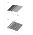
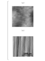
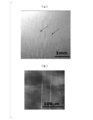
- FIG. 1 shows a normal AFM (Dimension made by Veeco Instrument).
- V shows a 10 ⁇ m square AFM image (stereoscopic surface perspective image) of the surface of the SiC epitaxial wafer.
- FIG. 1A is an AFM image showing conventional step bunching
- FIG. 1B is an AFM image showing short step bunching.
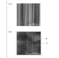
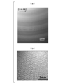
- FIG. 2 shows an AFM image of 200 ⁇ m ⁇ on the surface of the SiC epitaxial film observed by the wide-range observation type AFM (Nanoscale Hybrid Microscope VN-8000 manufactured by Keyence) used in the present invention.
- 2A is an AFM image showing conventional step bunching
- FIG. 2B is an AFM image showing short step bunching.
- FIG. 2 (a) it can be observed that the conventional step bunching exists at an average interval of about 1.5 ⁇ m as in the case of a normal AFM image.
- FIG. 2B shows that two lines (arrows B and C) are observed stably at equal intervals.
- the fact that the step can be stably observed in such a wide range of 200 ⁇ m ⁇ does not indicate mere noise or a peculiar surface area, and confirms the existence of step bunching having different properties from the conventional step bunching.
- optical surface inspection apparatus In order to confirm the presence of short step bunching with another surface inspection apparatus, observation was performed with an optical surface inspection apparatus using a laser beam (Candela CS20 manufactured by KLA-Tencor).
- This optical surface inspection apparatus is suitable for measuring the density of short step bunching because the entire surface of the wafer having a measurement range of several ⁇ m ⁇ to 4 inches ⁇ or more is larger than the wide-area observation type AFM.
- the optical surface inspection apparatus used in the present invention is a method in which laser light is incident on a wafer obliquely and scattered light from the wafer surface is reflected. It has the system which detects intensity
- the surface of the wafer is spiral scanned. Since the reflection position changes so as to trace the unevenness of the wafer surface, roughness (surface roughness) can be calculated from this position information.
- a 100 ⁇ m filter is used in the calculation, and long-period waviness information on the wafer surface is removed.
- step bunching is parallel to the [1-100] direction, a step is not detected in a region where the laser beam and the scanning direction are parallel during spiral scanning. Therefore, for the calculation of roughness information, a range of 70 ° between 55 ° to 125 ° and 235 ° to 305 ° in general polar coordinates is selected. Further, since the center of the spiral scan is a singular point where the laser beam hardly moves, the position information of the reflected light in the vicinity does not reflect the roughness. Therefore, the central ⁇ 10 mm range was excluded from the calculation area. The calculation range set in this way is about 35% of the entire wafer surface. However, with respect to step bunching, the morphology in this range almost reflects the entire wafer surface. Since the roughness calculated in this way has a correlation with the roughness measured using the AFM, it can be seen that the roughness is in accordance with the actual surface morphology.
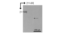
- FIG. 3 shows the observation result of the SiC epitaxial wafer in which short step bunching is observed with the optical surface inspection apparatus, using a differential interference microscope. As shown by the arrows, a noticeable shallow pit and accompanying short step bunching can be confirmed. The depth of the shallow pits on the epilayer surface was 6.3 nm.
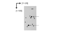
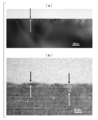
- FIG. 4 shows an observation result by a differential interference microscope after performing KOH etching to confirm the origin of the shallow pit.
- the presence of screw dislocations and the accompanying short step bunching can be confirmed. From this, it can be inferred that the short step bunching occurred as a result of step follow growth being hindered by the step of the shallow pit generated on the surface.
- the origin of the short step bunching is the shallow pit caused by the screw dislocation in the epi layer inherited from the substrate.
- the present inventors have observed this short step bunching on the surface by observing and evaluating the surface of the SiC epitaxial film by combining an optical surface inspection device and a surface inspection device different from the conventional one called a wide-range observation type AFM. It was found that it exists as a standard state, not a unique state. As a result of intensive studies, the present inventors have clarified the origin of short step bunching and suppressed the occurrence of the step bunching, thereby reaching a method for manufacturing a step bunching-free SiC epitaxial wafer.
- the short step bunching caused by the SiC single crystal substrate was discovered. Necessary conditions were found in the polishing process of the substrate. Then, the SiC single crystal substrate polished under such conditions is subjected to gas etching to clean the SiC single crystal substrate. If this SiC single crystal substrate is used, an amount of carbon-containing gas and silicon required for epitaxial growth of silicon carbide can be obtained. It has been found that conventional step bunching and short step bunching are remarkably reduced by simultaneously forming the film by supplying the contained gas to the substrate surface at a predetermined concentration ratio. Further, the inventors have found that a step bunching-free SiC epitaxial wafer can be obtained by simultaneously stopping the supply and maintaining the substrate temperature until the gas is removed and then lowering the temperature.
- the present invention provides the following means.
- SiC epitaxial wafer characterized in that is 1 piece / cm 2 or less.
- the film thickness distribution of the SiC epitaxial layer is 2% or less and the carrier concentration distribution is 10% or less, and the main surface of the SiC epitaxial wafer warps in a convex shape at room temperature,
- the “main surface” refers to a surface on which an epitaxial film is grown on a 4H—SiC single crystal substrate.
- the “film thickness distribution” and the “carrier concentration distribution” are obtained from ⁇ (maximum value ⁇ minimum value) / (maximum value + minimum value) ⁇ ⁇ 100 (%) using samples at a plurality of locations on the wafer.
- the growth temperature for epitaxial growth of the silicon carbide film is 1600 to 1640 ° C.
- the growth rate is 1 to 3 ⁇ m / h and the growth temperature is 1640 to 1700 ° C.
- the growth rate is 3 to 4 ⁇ m / h.
- the growth temperature is 1700 to 1800 ° C.
- the growth rate is (Ii)
- the growth temperature is 1600 to 1640 ° C.
- the production method of the SiC epitaxial wafer characterized in that. “Amount required for epitaxial growth of silicon carbide” means that desorption (sublimation) and adsorption (growth) of Si and C from the substrate occur simultaneously on the surface of the substrate at an elevated temperature.
- Gas separation occurs when the separation amount is greater than the adsorption amount, and growth occurs when the desorption amount is less than the adsorption amount.
- silicon-containing gas and / or the carbon-containing gas is added during the gas etching, these raw materials are used. Since the amount of gas is small, even if the source gas is added, only preferential gas etching occurs, so the difference from the supply amount of silicon-containing gas and / or carbon-containing gas during gas etching is clarified. It is an expression made with intent.
- the silicon-containing gas and the carbon-containing gas are supplied so that the atomic ratio C / Si of carbon to silicon in an amount required for epitaxial growth of silicon carbide is 0.7 to 1.2.
- the growth temperature for epitaxially growing the silicon carbide film is set to 1600 to 1640.
- the growth temperature is set to 1 ° C. to 1 ⁇ m / h
- the growth temperature is set to 1640 to 1700 ° C.
- the growth rate is set to 3 to 4 ⁇ m / h and the growth temperature is set to 1700 to 1800 ° C.
- the growth temperature for epitaxial growth of the silicon carbide film is 1600 to 1640 ° C.
- the growth rate is 2 to 4 ⁇ m / h
- the growth temperature is 1640 to 1700 ° C.
- the growth rate is 4 to 10 ⁇ m / h.
- the 700 ⁇ 1800 ° C. performs growth rate as 10 ⁇ 20 [mu] m / h
- the production method of the SiC epitaxial wafer according to item (5) characterized in that.
- Epitaxial growth of silicon carbide film (1) When a 4H—SiC single crystal substrate with an off angle of 0.4 ° to 2 ° is used, when the growth temperature for epitaxial growth of the silicon carbide film is 1600 to 1640 ° C., When the growth rate is 1 to 3 ⁇ m / h and the growth temperature is 1640 to 1700 ° C., the growth rate is 3 to 4 ⁇ m / h. When the growth temperature is 1700 to 1800 ° C., the growth rate is 4 (2) When a 4H—SiC single crystal substrate with an off angle of 2 ° to 5 ° is used, the growth rate is 1600 to 1640 ° C. when the growth temperature for epitaxial growth of the silicon carbide film is 1600 to 1640 ° C.
- the growth rate is 4 to 10 ⁇ m / h and the growth temperature is 1700 to 1800 ° C.
- the growth rate is 4 to 10 ⁇ m / h and the growth temperature is 1700 to 1800 ° C.
- the growth rate is 10 ⁇ 20 [mu] m / h
- triangular defect density on the surface of the SiC epitaxial layer has a 1 / cm 2 or less, the density of stacking faults of SiC epitaxial wafer layer The effect that a SiC epitaxial wafer of 1 piece / cm 2 or less is obtained is obtained.
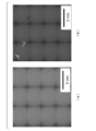
- SiC epitaxial wafer of 4 degrees off angle with the photo-luminescence imaging device (a) SiC epitaxial wafer of this invention, (b) The image which shows the conventional SiC epitaxial wafer. It is (a) image and (b) defect map which measured C surface of the SiC epitaxial wafer of the conventional 0.8 degree off angle
- SiC epitaxial wafer 5 and 6, the SiC epitaxial wafer according to the embodiment of the present invention, in which the SiC epitaxial layer is formed on the Si surface of the 4H—SiC single crystal substrate inclined at an off angle of 4 °, is observed over a wide range.
- the results of observation with an optical surface inspection apparatus (Candela CS20 manufactured by KLA-Tencor) using a type AFM and laser light are shown.
- FIG. 5 (a) is a 200 ⁇ m ⁇ wide observation type AFM image of the surface of the SiC epitaxial wafer of the present invention.
- FIG. 5 (b) shows a 200 ⁇ m ⁇ wide-range observation type AFM image of the surface of a conventional SiC epitaxial wafer.
- step linear density 0 / mm ⁇ 1
- few steps were observed for other areas of this sample. Therefore, step bunching free is realized, and it can be seen that the linear density of the step is 5 mm ⁇ 1 or less.
- the root mean square roughness Rq was 0.5 nm
- the maximum height difference Ry was 0.8 nm.
- the average Rq of three regions selected at random in the same sample was 0.41 nm, and the average Ry was 0.82 nm. Therefore, it can be seen that the observed root mean square roughness Rq is 1.0 nm or less and the maximum height difference Ry is 3.0 nm or less.
- step bunching in which a large number of steps were combined at a linear density of 340 lines / mm ⁇ 1 was observed.
- the average step line density of the other three regions of this sample was 362 lines / mm ⁇ 1 . It can also be seen that the steps extend beyond the observation range.
- the root mean square roughness Rq was 2.4 nm
- the maximum height difference Ry was 3.6 nm.
- the average Rq of three regions randomly selected from the same sample was 3.2 nm, and the average Ry was 4.5 nm.
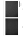
- FIGS. 6 (a) and 6 (b) are images observed by an optical surface inspection apparatus using laser light (hereinafter referred to as “candela image”) for the 1 mm ⁇ range of the same sample in FIGS. 5 (a) and 5 (b), respectively. ).
- the observed root mean square roughness Rq of the SiC epitaxial wafer of the present invention was 0.54 nm. On the other hand, it is 1.7 nm in the conventional SiC epitaxial wafer, and it can be seen that there is a clear difference in surface flatness between the present invention and the conventional SiC epitaxial wafer.
- FIG. 7A shows a photoluminescence imaging apparatus (photon design) of a SiC epitaxial wafer of the present invention in which a SiC epitaxial layer is formed on the Si surface of a 4H—SiC single crystal substrate inclined at an off angle of 4 °.
- the PL image observed with PLI-100 manufactured by the company is shown.
- FIG. 7B shows a photoluminescence imaging device (SiC epitaxial wafer) in which a SiC epitaxial wafer is formed by forming a SiC epitaxial layer on a Si surface of a 4H—SiC single crystal substrate inclined at an off angle of 4 ° by a conventional method.
- a PL image image observed with PLI-100 manufactured by Photon Design Co., Ltd. is shown.
- the stacking fault density was 0 / cm 2 .
- the stacking fault density was 2.8 / cm 2 .
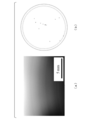
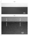
- an SiC epitaxial layer is formed on the C-plane of a 4H—SiC single crystal substrate tilted at an off angle of 0.8 °, which is an embodiment of the present invention.
- the results (candela image (a)) and defect map (b) based on the candela image of the epitaxial wafer observed with an optical surface inspection apparatus (Candela CS20 manufactured by KLA-Tencor) are shown.
- an optical surface inspection apparatus (Candela CS20 manufactured by KLA-Tencor)
- the triangular defect density is 0.4 / cm 2 (the defect density including the triangular defect is 1.2 / cm 2 ). It can be seen that it is significantly reduced as compared with the conventional SiC epitaxial wafer shown in FIG. In particular, the reduction in the peripheral region of the wafer is large. This is considered to be due to the effect of epitaxial growth using a 4H—SiC single crystal substrate whose main surface is processed into a convex shape while reducing the dent (warpage) of the substrate during epitaxial growth. It is considered that the defect density in the central part is further reduced by processing into a convex shape having an optimal curvature radius.
- FIG. 10A shows a PL image of the SiC epitaxial wafer according to the embodiment of the present invention shown in FIG. 9 observed with a photoluminescence imaging apparatus (PLI-100 manufactured by Photon Design).
- FIG. 10B is a PL image of a SiC epitaxial wafer manufactured by the conventional method shown in FIG.
- the stacking fault density was 0.1 / cm 2 .
- the SiC epitaxial wafer according to the conventional method shown in FIG. 10B three triangular light emission / absorptions are observed, and stacking faults exist.
- the stacking fault density was 1.8 / cm 2 .
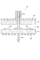
- FIG. 11 is a schematic diagram of an example of an apparatus for forming an SiC epitaxial wafer film of the present invention.
- This silicon carbide film forming apparatus 101 penetrates through a reaction chamber 104 provided between a planetary 102 and a heat radiation member 103 that supports a plurality of wafer placement portions 102b, and a central portion of the heat radiation member 103.
- the gas supply part 105 which supplies gas in the reaction chamber 104, and the high frequency coils 106 and 107 which heat the planetary 102 and the heat radiation member 103, respectively are provided.
- the revolution rotating shaft 102 a is disposed directly below the gas supply unit 105.
- the SiC single crystal wafer is revolved at a rotational speed of, for example, 5 to 20 rpm by the planetary 102 with the gas supply unit 105 as the central axis, and the SiC single crystal wafer itself is centered on the center of the SiC single crystal wafer.
- the wafer mounting unit 102b rotates at a rotational speed of 50 to 200 rpm.
- the wafer installation portion 102b and the planetary 102 are rotated by themselves to improve the in-plane uniformity of the SiC wafer thickness, carrier concentration, and temperature distribution.
- the substrate can be heated to a high temperature by the configuration in which the high-frequency coils 106 and 107 are arranged above and below the reaction chamber 104.
- the wafer mounting portion 102b is set with the growth surface (front surface) formed in a convex shape of the SiC wafer facing up.
- a temperature difference occurs between the front surface and the back surface of the SiC wafer. This is because the front surface of the substrate is cooled by the gas supplied from the gas supply unit 105.
- the substrate is warped due to a difference in thermal expansion caused by the temperature difference between the front surface and the back surface, and as a result, a part of the SiC wafer is floated from the wafer setting portion 102b, and the applied heat is generated by the SiC. Not transmitted evenly across the wafer.
- Fabrication of the SiC single crystal substrate (wafer) starts by slicing a 4H—SiC ingot manufactured by a method such as a sublimation method. Slicing is usually performed with an inner peripheral blade or a wire saw, but in recent years, a wire saw with good mass productivity is generally used. When performing convex processing, convex processing is performed in the stage of this slice.
- the amount of deflection of the wire at the time of cutting is set to 2 mm or more, and by tilting the angle formed by the plane perpendicular to the outer periphery of the cylindrical ingot with respect to the plane including the straight line formed by the wire reciprocating direction, from the ingot
- the shape of at least one surface of the SiC single crystal wafer to be cut out can be processed into a convex shape.
- the convex curvature radius is in the range of 10 m or more and 1000 m or less.
- the inclination angle is changed so that the convex direction becomes a surface used for the epitaxial surface.
- the SiC single crystal substrate processed into a convex shape is continuously and uniformly convex on the main surface.
- Continuously and uniformly convex means that there are no angular portions and a smooth state, and there are no portions that are partially concave.
- the convex curvature radius is preferably in the range of 10 m to 1000 m. This is because if it is 10 m or less, the depression of the main surface at room temperature cannot be sufficiently reduced by thermal expansion during epitaxial growth, and if it is 1000 m or more, the effect of the convex (curved) processing is not sufficient. There are several methods of measuring and quantifying the size of the convex shape (curvature, warpage).
- the curvature radius of the convex shape is measured by a wafer flatness measurement analyzer (for example, manufactured by S-Oel Corporation) It can be determined from Warp measured by UltraSort). Warp is defined as the sum of the maximum deviations in the vertical direction from the focal plane, with the focal plane as the reference plane, in a free state where the wafer is not chucked as a measurement method. Is one of the commonly used indicators.
- the Warp measurement value matches the warp value in the general definition.
- the SiC single crystal substrate may be one that satisfies either one of the main surface being curved or the SiC single crystal substrate itself being warped convexly toward the main surface.
- the main surface may be curved and the SiC single crystal substrate itself may be convexly warped.
- the 4H—SiC single crystal substrate remaining on the wafer surface in the slicing step is polished until the lattice disorder layer on the surface becomes 3 nm or less.
- the “lattice disordered layer” has a striped structure corresponding to the atomic layer (lattice) of the SiC single crystal or a part of the stripe in the TEM lattice image (image in which the lattice can be confirmed). Refers to no layer.
- FIGS. 12 and 13 show transmission electron microscope (TEM) images near the surface of the SiC single crystal substrate after the polishing step.
- FIG. 12 (a) and 12 (b) are TEM images showing examples of the SiC single crystal substrate of the present invention.
- the surface flatness disorder cannot be observed.
- FIG. 12B which is an enlarged image, disorder is observed only in the uppermost atomic layer (lattice), and a clear striped structure is observed from the lower atomic layer (lattice). it can.
- a layer sandwiched by arrows is a “lattice disorder layer”. From this TEM image, it can be confirmed that the “lattice disordered layer” on the surface is 3 nm or less.
- FIGS. 13A and 13B are TEM images showing an example of a SiC single crystal substrate having a lattice disorder layer of 3 nm or more on the surface.
- a clear disturbance of surface flatness is observed, and a lattice image (FIG. 13B) which is an enlarged image of a portion which appears flat in FIG. 13A.
- FIG. 5 the disturbance of the stripe structure can be observed over 6 nm from the surface.
- a “lattice disorder layer” of about 7 nm (a layer sandwiched between arrows on the right side in the image) can be observed, and it can be seen that the surface “lattice disorder layer” cannot achieve 3 nm or less in this sample. .
- the polishing process includes a plurality of polishing processes such as rough polishing usually called lapping, precision polishing called polishing, and chemical mechanical polishing (hereinafter referred to as CMP) which is ultra-precision polishing.
- the polishing process is often performed in a wet manner, but the common process in this process is to apply a polishing head to which a silicon carbide substrate is bonded while supplying polishing slurry to a rotating surface plate to which a polishing cloth is attached. Is to be done.
- the polishing slurry used in the present invention is basically used in such a form, but the form is not limited as long as it is wet polishing using the polishing slurry.
- the particles used as the abrasive grains may be particles that do not dissolve and disperse in this pH range.
- the pH of the polishing liquid is preferably less than 2.
- diamond, silicon carbide, aluminum oxide, titanium oxide, silicon oxide, or the like can be used as the abrasive particles.
- abrasive particles having an average diameter of 1 to 400 nm, preferably 10 to 200 nm, more preferably 10 to 150 nm are used as abrasive grains.
- silica is preferred in that small particles are commercially available at low cost. More preferred is colloidal silica.
- the particle size of an abrasive such as colloidal silica can be appropriately selected depending on processing characteristics such as processing speed and surface roughness. When a higher polishing rate is required, an abrasive having a large particle size can be used. When the surface roughness is small, that is, when a highly smooth surface is required, an abrasive having a small particle diameter can be used. Those having an average particle diameter exceeding 400 nm are expensive because they are expensive and the polishing rate is not high. When the particle diameter is extremely small such as less than 1 nm, the polishing rate is remarkably reduced.
- the addition amount of abrasive particles is 1% by mass to 30% by mass, preferably 1.5% by mass to 15% by mass. If it exceeds 30% by mass, the drying speed of the abrasive particles becomes high, which increases the risk of causing scratches, and is uneconomical. Further, if the abrasive particles are less than 1% by mass, the processing speed becomes too low, which is not preferable.
- the polishing slurry in the present invention is a water-based polishing slurry, and the pH at 20 ° C. is less than 2.0, desirably less than 1.5, and more desirably less than 1.2. In the region where the pH is 2.0 or more, a sufficient polishing rate cannot be obtained.
- the slurry less than pH 2 the chemical reactivity with respect to silicon carbide is remarkably increased even under a normal indoor environment, and ultraprecision polishing becomes possible.
- the silicon carbide is not directly removed by the mechanical action of the oxide particles in the polishing slurry, but the polishing liquid causes the silicon carbide single crystal surface to chemically react with the silicon oxide, and the silicon oxide is mechanically treated by the abrasive grains.
- polishing composition liquid so that silicon carbide can easily react, that is, setting the pH to less than 2, and selecting oxide particles having an appropriate hardness as abrasive grains can cause scratching and processing. It is very important to obtain a smooth surface without an altered layer.
- the polishing slurry is adjusted to have a pH of less than 2 using at least one acid, preferably two or more acids.
- an inorganic acid is preferable, and as the inorganic acid, hydrochloric acid, nitric acid, phosphoric acid, and sulfuric acid are preferable.
- the reason why it is effective to use a plurality of acids is unknown, but it has been confirmed by experiments, and there is a possibility that a plurality of acids interact with each other and enhance the effect.
- the amount of acid added is, for example, within the range of 0.5 to 5% by mass of sulfuric acid, 0.5 to 5% by mass of phosphoric acid, 0.5 to 5% by mass of nitric acid, and 0.5 to 5% by mass of hydrochloric acid.
- the type and amount are selected so that the pH is less than 2.
- the inorganic acid is effective because it is a stronger acid than the organic acid and is extremely convenient for adjusting to a predetermined strongly acidic polishing liquid. If an organic acid is used, it is difficult to adjust the strongly acidic polishing liquid.
- the polishing of silicon carbide is performed by removing the oxide layer with oxide particles due to the reactivity to the oxide film generated on the surface of silicon carbide by the strongly acidic polishing liquid. In order to accelerate this surface oxidation, polishing is performed.
- an oxidizing agent is added to the slurry, a further excellent effect is recognized.
- the oxidizing agent include hydrogen peroxide, perchloric acid, potassium dichromate, ammonium persulfate sulfate, and the like.
- the polishing rate is improved by adding 0.5 to 5% by mass, preferably 1.5 to 4% by mass, but the oxidizing agent is not limited to hydrogen peroxide solution. .
- an anti-gelling agent can be added to suppress gelation of the abrasive.
- phosphate ester type chelating agents such as 1-hydroxyethylidene-1,1-diphosphonic acid and aminotriethylenephosphonic acid are preferably used.
- the anti-gelling agent is added in the range of 0.01 to 6% by mass, preferably 0.05 to 2% by mass.
- the damage pressure is reduced to 50 nm by using a polishing pressure of 350 g / cm 2 or less and using abrasive grains having a diameter of 5 ⁇ m or less in mechanical polishing before CMP.
- the polishing slurry contains abrasive particles having an average particle diameter of 10 nm to 150 nm and an inorganic acid, and preferably has a pH of less than 2 at 20 ° C.
- Silica more preferably 1 to 30% by mass, and more preferably at least one of inorganic acid, hydrochloric acid, nitric acid, phosphoric acid and sulfuric acid.
- the gas etching is performed for 5 to 30 minutes while maintaining the SiC single crystal substrate at 1400 to 1800 ° C., the hydrogen gas flow rate of 40 to 120 slm, and the pressure of 100 to 250 mbar.
- the substrate After cleaning the polished SiC single crystal substrate, the substrate is set in an epitaxial growth apparatus, for example, a mass production type multiple planetary CVD apparatus. After introducing hydrogen gas into the apparatus, the pressure is adjusted to 100 to 250 mbar. Thereafter, the temperature of the apparatus is raised, the substrate temperature is set to 1400 to 1600 ° C., preferably 1480 ° C. or higher, and gas etching of the substrate surface is performed with hydrogen gas for 1 to 30 minutes. When gas etching with hydrogen gas is performed under such conditions, the etching amount is about 0.05 to 0.4 ⁇ m.
- an epitaxial growth apparatus for example, a mass production type multiple planetary CVD apparatus.
- the pressure is adjusted to 100 to 250 mbar.
- the temperature of the apparatus is raised, the substrate temperature is set to 1400 to 1600 ° C., preferably 1480 ° C. or higher, and gas etching of the substrate surface is performed with hydrogen gas for 1 to 30 minutes.
- the etching amount is about 0.05 to 0.4
- the substrate surface is damaged by the polishing process, and it is considered that not only damage that can be detected as a “lattice disorder layer” in the TEM but also distortion of the lattice that cannot be detected by the TEM exists.
- the purpose of gas etching is to remove the layer damaged in this way (hereinafter also referred to as “damage layer”).
- the gas etching is not sufficient and the damaged layer remains, dissimilar polytypes are present in the epitaxial growth layer. And dislocations and stacking faults are introduced. Further, if etching is performed too much, surface reconstruction occurs on the substrate surface, and step bunching occurs before the start of epitaxial growth. For this reason, it is important to optimize the damaged layer and the amount of gas etching.
- the present inventors have found that as a sufficient condition in the production of a step bunching-free SiC epitaxial wafer, They found a combination of the damage layer when the layer was thinned to 3 nm or less and the gas etching conditions described above.
- the root mean square roughness Rq of the outermost surface of the epitaxial layer obtained by analyzing an area of 35% or more of the entire wafer surface using an optical surface inspection apparatus is 1.3 nm or less. I can confirm that.
- the step bunching is 1.0 nm or less at 10 ⁇ m ⁇ , 1.0 nm or less at 200 ⁇ m ⁇ , and a length of 100 to 500 ⁇ m observed at 200 ⁇ m ⁇ . It can be confirmed that the maximum height difference Ry in (short step bunching) is 3.0 nm or less. It can also be confirmed that the linear density of this step is 5 mm ⁇ 1 or less. It is important to maintain the flatness of the substrate surface in the subsequent film forming process and temperature lowering process.
- SiH 4 gas and / or C 3 H 8 gas may be added to the hydrogen gas.
- SiH 4 gas having a concentration of less than 0.009 mol% is added to hydrogen gas to make the environment in the reactor Si-rich.
- the depth of the shallow pit can be reduced, and the occurrence of short step bunching associated with the shallow pit can be suppressed.
- SiH 4 gas and / or C 3 H 8 gas it is preferable to evacuate once to form a hydrogen gas atmosphere before the film formation (epitaxial growth) step.
- ⁇ Film formation (epitaxial growth) process In the film formation (epitaxial growth) step (after the temperature rise when the growth temperature of the epitaxial film is higher than the cleaning (gas etching) temperature), it is required for the epitaxial growth of silicon carbide on the surface of the cleaned substrate.
- a quantity of SiH 4 gas and C 3 H 8 gas are simultaneously supplied at a concentration ratio C / Si of 0.7 to 1.2 to epitaxially grow silicon carbide.
- “simultaneous supply” means that supply is not required until the time is completely the same, but is supplied with a difference within several seconds.
- Hot Wall SiC CVD VP2400HW
- step bunching-free SiC epitaxial wafer could be manufactured.
- Each flow rate, pressure, substrate temperature, and growth temperature of SiH 4 gas and C 3 H 8 gas are 15 to 150 sccm, 3.5 to 60 sccm, 80 to 250 mbar, higher than 1600 ° C. and lower than 1800 ° C., and the growth rate is 1 hour / hour. It is determined within the range of ⁇ 20 ⁇ m while controlling the off angle, film thickness, carrier concentration uniformity, and growth rate.
- the carrier concentration in the epitaxial layer can be controlled.
- the epitaxial layer to be grown usually has a film thickness of about 5 to 20 ⁇ m and a carrier concentration of about 2 to 15 ⁇ 10 15 cm ⁇ 3 .
- the growth temperature and growth rate depend on the off angle of the SiC single crystal substrate.
- the growth is performed by epitaxially growing a silicon carbide film.
- the temperature is 1600 to 1640 ° C.
- the growth rate is 1 to 3 ⁇ m / h.
- the growth temperature is 1640 to 1700 ° C.
- the growth rate is 3 to 4 ⁇ m / h
- the growth temperature is 1700 to 1700 ° C.
- the growth rate is 4 to 10 ⁇ m / h.
- the growth temperature for epitaxial growth of the silicon carbide film is set.
- the growth rate is 1600 to 1640 ° C.
- the growth rate is 2 to 4 ⁇ m / h.
- the growth temperature is 1640 to 1700 ° C.
- the growth rate is 4 to 10 ⁇ m / h.
- the degrees and 1700 ⁇ 1800 ° C. performs growth rate as 10 ⁇ 20 ⁇ m / h.
- the supply of SiH 4 gas and C 3 H 8 gas and the introduction of nitrogen gas as a doping gas are stopped and the temperature is lowered.
- gas etching occurs on the surface of the SiC epitaxial film, deteriorating the surface morphology. obtain.
- the timing of stopping the supply of the SiH 4 gas and the C 3 H 8 gas and the timing of temperature decrease are important. By simultaneously stopping the supply of SiH 4 gas and C 3 H 8 gas, holding the growth temperature until these supplied gases disappear from the substrate surface, and then lowering the temperature to room temperature at an average rate of about 50 ° C. It was found that deterioration of morphology was suppressed.
- SiH 4 gas as a silicon-containing gas and C 3 H 8 gas as a carbon-containing gas, N 2 gas as a doping gas, H 2 gas as a carrier gas and an etching gas are used, and a mass production type multiple-planetary is used.
- Example 1 A SiC epitaxial layer is formed on the Si surface of a 4H—SiC single crystal substrate inclined at an off angle of 4 °.
- the 4H—SiC single crystal substrate is not subjected to convex processing.
- mechanical polishing before CMP was performed at a processing pressure of 350 g / cm 2 using abrasive grains having a diameter of 5 ⁇ m or less.
- CMP was performed for 30 minutes using silica particles having an average particle diameter of 10 to 150 nm as abrasive particles, a slurry containing sulfuric acid as an inorganic acid and a pH of 1.9 at 20 ° C. Thereby, the lattice disorder layer on the surface was made 3 nm or less.
- the polished substrate was introduced into the growth apparatus after RCA cleaning.
- the RCA cleaning is a wet cleaning method generally used for Si wafers, and a substrate is prepared by using a mixed solution of sulfuric acid / ammonia / hydrochloric acid and hydrogen peroxide solution and a hydrofluoric acid aqueous solution. Organic substances, heavy metals and particles on the surface can be removed.
- the cleaning (gas etching) step was performed at a hydrogen gas flow rate of 100 slm, a reactor internal pressure of 200 mbar, and a substrate temperature of 1500 ° C. for 20 minutes.
- the substrate temperature is set to 1650 ° C.
- C 3 H 8 gas 24 sccm and SiH 4 gas 8 sccm are simultaneously started so that SiH 4 gas and C 3 H 8 gas are simultaneously supplied to the main surface of the substrate. went.
- C / Si was selected to be 1.0.
- a SiC epitaxial layer having a thickness of 10 ⁇ m was formed by carrying out a growth process for 2 hours at a growth rate of 5 ⁇ m / h with the pressure in the reactor set to 200 mbar.
- a wide-area observation type AFM Keyence Nanoscale Hybrid Microscope VN-8000
- an optical surface inspection device KLA-Tencor Candela CS20
- a photoluminescence imaging device Photon Design
- Rq measured by the optical surface inspection apparatus was 1.2 nm
- Rq measured by the wide-range observation type AFM was 0.4 nm
- the maximum height difference Ry was 0.6 nm
- step bunching was not observed.
- the density of triangular defects on the surface of the epitaxial film of the SiC epitaxial wafer was 0.6 / cm 2
- the density of stacking faults in the film of the epitaxial film of the SiC epitaxial wafer was 0 / cm 2 .
- the production conditions of the SiC epitaxial wafer are the same as those in Example 1 except that the substrate growth temperature is 1600 ° C.
- the SiC epitaxial wafer thus manufactured was measured with an optical surface inspection device (Candela CS20 manufactured by KLA-Tencor) and a photoluminescence imaging device (PLI-100 manufactured by Photon Design).
- an optical surface inspection device Candela CS20 manufactured by KLA-Tencor
- a photoluminescence imaging device PLI-100 manufactured by Photon Design
- triangular defects on the surface of the SiC epitaxial wafer were measured.
- the density was 2.4 / cm 2 , and triangular defects were present throughout the wafer.
- the stacking fault density in the film of the SiC epitaxial wafer is 2.8 / cm 2, which is considerably larger than that of the first embodiment of the present invention. From this comparison, it was found that there is a growth temperature that reduces the defect density at a temperature higher than the upper limit (1600 ° C.) of the
- Example 2 [Si surface of 4H-SiC single crystal substrate with an off angle of 1.2 °] (Example 2)
- a SiC epitaxial wafer was fabricated under the same fabrication conditions as in Example 1 except that the growth process was performed at a growth rate of 4 ⁇ m / h for 2.5 hours.
- an optical surface inspection apparatus (Candela CS20 manufactured by KLA-Tencor), a photoluminescence imaging apparatus (PLI-100 manufactured by Photon Design), and a wide-range observation type AFM (Nanoscale hybrid microscope manufactured by Keyence) VN-8000).
- the triangular defect density was 0.4 / cm 2
- the stacking fault density was 0.1 / cm 2 . Step bunching was not observed. All of them were 1 piece / cm 2 or less, and an extremely high quality epitaxial film having a low defect density was formed on a 4H—SiC single crystal substrate having an off angle of 1.2 °, which is lower than that of Example 1.
- Example 3 [C-plane of 4H-SiC single crystal substrate with off angle of 0.8 °] (Example 3)
- Example 1 except that the Si surface was sliced into a convex shape using a multi-wire saw so that the convex curvature radius was 50 m, and the growth step was performed at a growth rate of 4 ⁇ m / h for 2.5 hours.
- a SiC epitaxial wafer was produced under the same production conditions. With respect to the manufactured SiC epitaxial wafer, the results of measurement with an optical surface inspection apparatus (Candela CS20 manufactured by KLA-Tencor) and photoluminescence imaging apparatus (PLI-100 manufactured by Photon Design) are as shown in FIG. It is.
- an optical surface inspection apparatus Candela CS20 manufactured by KLA-Tencor
- PLI-100 photoluminescence imaging apparatus manufactured by Photon Design
- the triangular defect density was 0.4 / cm 2
- the stacking fault density was 0.2 / cm 2
- an extremely high quality epitaxial film having a defect density of 1 piece / cm 2 or less and having a low defect density was formed on the Si surface of the 4H—SiC single crystal substrate having a low off-angle.
- step bunching was not observed in the measurement using the optical surface inspection apparatus (Candela CS20 manufactured by KLA-Tencor) and the wide-area observation type AFM (Nanoscale hybrid microscope VN-8000 manufactured by Keyence).
- a mercury probe concentration analyzer (Hg-CV) (495 CV SYSTEM manufactured by SSSM) was used, and for the carrier concentration uniformity, a fast Fourier transform infrared absorption analyzer (FT-IR) (QS1200 manufactured by Nanometrics). ).
- the film thickness uniformity was 2%, the carrier concentration uniformity was 8%, and a SiC epitaxial layer with good in-plane uniformity was formed.
- “Film thickness distribution” and “carrier concentration distribution” were obtained from ⁇ (maximum value ⁇ minimum value) / (maximum value + minimum value) ⁇ ⁇ 100 (%) using eight samples on the wafer. is there.
- the film thickness uniformity is about 5 to 10%, and the carrier concentration uniformity is about 15 to 20%. Improved uniformity.
- Example 2 The production conditions of the SiC epitaxial wafer are the same as those in Example 3 except that the substrate growth temperature is 1600 ° C.
- the SiC epitaxial wafer thus produced was measured with an optical surface inspection apparatus (Candela CS20 manufactured by KLA-Tencor) and a photoluminescence imaging apparatus (PLI-100 manufactured by Photon Design). The results are shown in FIGS.
- the density of triangular defects on the surface of the SiC epitaxial wafer was 4 / cm 2 , and there were triangular defects throughout the wafer.
- the stacking fault density in the film of the SiC epitaxial wafer is 1.8 / cm 2, which is considerably higher than that of Example 3 of the present invention. From this comparison, it was found that there is a growth temperature that reduces the defect density at a temperature higher than the upper limit (1600 ° C.) of the conventional growth temperature.
- An SiC epitaxial film was grown on a Si surface inclined by 4 ° in the ⁇ 11-20> axis direction with respect to the (0001) plane of the 4H—SiC single crystal by Hot Wall SiC CVD (VP2400HW).
- an optical surface inspection apparatus (Candela CS20 manufactured by KLA-Tencor), a normal AFM (Dimension V manufactured by Veeco Instrument) and a wide-area observation type AFM (Nanoscale hybrid microscope manufactured by Keyence) VN-8000).
- Example 1 The polishing step and subsequent cleaning were performed under the same conditions as in Example 1.
- the cleaning (gas etching) step was carried out at a hydrogen gas flow rate of 90 slm, a reactor pressure of 200 mbar, and a substrate temperature of 1550 ° C. for 10 minutes.
- SiH 4 gas is supplied after 3 seconds. did. C / Si selected 1.1.
- a growth process was performed for 2 hours at a growth rate of 5 ⁇ m / h with a reactor internal pressure of 200 mbar and a substrate temperature of 1550 ° C., thereby forming a 10 ⁇ m thick SiC epitaxial layer.
- the Rq measured with the wide-area observation type AFM and the optical surface inspection apparatus was 1.2 nm, and the Rq measured with the wide-area observation type AFM was Rq. It was 0.4 nm, the maximum height difference Ry was 0.7 nm, and no step bunching was observed.
- Sample 2 A SiC epitaxial wafer was manufactured under the same conditions as in Sample 1 except for gas etching conditions.
- the gas etching step is different from Sample 1 in that SiH 4 gas having a concentration of 0.008 mol% is added to hydrogen gas.
- the SiC epitaxial wafer thus produced was measured with an optical surface inspection apparatus and a wide-area observation type AFM.
- An image similar to Sample 1 was observed, Rq measured with an optical surface inspection apparatus was 1.1 nm, Rq measured with a wide-range observation type AFM was 0.4 nm, and the maximum height difference Ry was 0.7 nm. .
- FIGS. 6B and 5B Images of the manufactured SiC epitaxial wafer measured by an optical surface inspection apparatus and a wide-area observation type AFM are as shown in FIGS. 6B and 5B, respectively.
- the root mean square roughness Rq measured by the optical surface inspection apparatus was 1.7 nm
- the root mean square roughness Rq measured by the wide-range observation type AFM was 2.4 nm
- the maximum height difference Ry was 3.6 nm. .
- FIGS. 14A and 14B show a candela image and a wide-range observation type AFM image for the manufactured SiC epitaxial wafer.
- the root mean square roughness Rq measured by the optical surface inspection apparatus was 1.4 nm
- the root mean square roughness Rq measured by the wide range observation type AFM was 1.4 nm
- the maximum height difference Ry was 2.8 nm.
- the linear density of the step was 10 pieces / mm ⁇ 1 .
- the SiC epitaxial wafer of the present invention is a step-bunching-free SiC epitaxial wafer in which triangular defects and stacking faults are reduced, the carrier concentration and film thickness are high, and various devices such as power devices, high-frequency devices, and high-temperature operation devices. It can be used for the manufacture of a silicon carbide semiconductor device.
Abstract
Description
本願は、2009年12月14日に、日本に出願された特願2009-283113号に基づき優先権を主張し、その内容をここに援用する。 The present invention relates to a SiC epitaxial wafer and a manufacturing method thereof, and particularly to a high-quality SiC epitaxial wafer having a low defect density, a high uniformity of film thickness and carrier concentration, and no step bunching, and a manufacturing method thereof.
This application claims priority based on Japanese Patent Application No. 2009-283113 for which it applied to Japan on December 14, 2009, and uses the content here.
エピタキシャル膜中には基板に用いているポリタイプと異なるポリタイプが混入しやすく、例えば、基板に4H-SiCを使った場合には3C-SiCや8H-SiCが混入する。異なるポリタイプの混入は結晶格子の積層構造を乱し、積層欠陥となる。
エピタキシャル成長は、これらの混入を抑制するため、SiC単結晶基板を微傾斜させてステップフロー成長(原子ステップからの横方向成長)させて行うのが一般的であるが、速い成長速度を持つステップが遅い成長速度を持つステップに追いついて合体し、ステップバンチングが発生する。 SiC has many polytypes, but 4H—SiC is mainly used to fabricate practical SiC devices. A SiC single crystal wafer processed from a bulk crystal produced by a sublimation method or the like is used as the substrate of the SiC device, and an SiC epitaxial film that becomes an active region of the SiC device is usually formed thereon by chemical vapor deposition (CVD). Form.
A polytype different from the polytype used for the substrate is likely to be mixed in the epitaxial film. For example, when 4H—SiC is used for the substrate, 3C—SiC or 8H—SiC is mixed. The mixing of different polytypes disturbs the laminated structure of the crystal lattice, resulting in a stacking fault.
Epitaxial growth is generally performed by step-flow growth (lateral growth from atomic steps) by slightly tilting a SiC single crystal substrate in order to suppress these contaminations, but there are steps with a high growth rate. Step bunching occurs after catching up with a step having a slow growth rate and coalescing.
SiC基板が2インチ程度までのサイズの場合では SiC単結晶基板のオフ角は主に8°が用いられてきた。このオフ角においてはウェハ表面のテラス幅が小さく、容易にステップフロー成長が得られるが、オフ角が大きいほど、SiCインゴットから得られるウェハ枚数が少なくなる。そのため、3インチ以上のSiC基板においては、主に4°程度のオフ角のものが用いられている。
コスト削減の観点から、さらなる低オフ角、最も望ましくはステップフロー成長をさせることが可能なオフ角として知られる0.4°程度の微傾斜オフ角SiC単結晶基板上のエピタキシャル成長技術の確立が求められている。 <Epitaxial growth on low off-angle SiC single crystal substrate>
In the case where the SiC substrate has a size up to about 2 inches, the off-angle of the SiC single crystal substrate has been mainly 8 °. At this off-angle, the terrace width on the wafer surface is small and step flow growth can be easily obtained. However, the larger the off-angle, the smaller the number of wafers obtained from the SiC ingot. For this reason, SiC substrates having an off angle of about 4 ° are mainly used for SiC substrates of 3 inches or more.
From the viewpoint of cost reduction, establishment of an epitaxial growth technique on a SiC single crystal substrate having a slightly lower off-angle, and most preferably a finely inclined off-angle of about 0.4 °, which is known as an off-angle capable of performing step flow growth, is required. It has been.
また、例えば、0.4°のオフ角のウェハでは4°のオフ角のウェハに比べてテラス幅は10倍になり、ステップフロー成長させる長さが一桁長くなるので、従来用いられてきた常識的なステップフロー成長の条件がそのまま使えないおそれがある。 However, the lower the off angle, the larger the terrace width of the surface of the SiC single crystal substrate (wafer). Therefore, the migration rate of migration atoms taken into the step end, that is, the growth rate of the step end tends to vary. As a result, there is a problem that a step with a fast growth rate catches up with a step with a slow growth rate, and step bunching occurs. In particular, when the epitaxial surface is a Si surface, the migration of surface atoms is suppressed as compared with the C surface, so that step bunching occurs easily. Reduction of step bunching is a major issue for the use of low off-angle SiC single crystal substrates.
In addition, for example, a 0.4 ° off-angle wafer has a terrace width 10 times that of a 4 ° off-angle wafer, and the step flow growth length is an order of magnitude longer. There is a possibility that common-sense step flow growth conditions cannot be used as they are.
ステップバンチングとは、表面において原子ステップ(通常2~10原子層程度)が集まって合体する現象をいい、この表面の段差自体を指すこともある。非特許文献2に典型的なステップバンチングが示されている。
従来、ステップバンチングの観察・評価は、微分干渉顕微鏡等の光学顕微鏡と原子分解能を有する原子間力顕微鏡(AFM)との組み合わせで行われることが多かった(例えば、非特許文献2、3)。 <Step bunching and its observation and evaluation>
Step bunching refers to a phenomenon in which atomic steps (usually about 2 to 10 atomic layers) gather and coalesce on the surface, and sometimes refers to the surface step itself. Non-patent
Conventionally, observation and evaluation of step bunching has often been performed by a combination of an optical microscope such as a differential interference microscope and an atomic force microscope (AFM) having atomic resolution (for example, Non-Patent
本明細書において「三角欠陥」とは、SiC単結晶基板を微傾斜させる[11-20]方向に垂直に辺を有する略三角形状の欠陥であって、エピタキシャル膜の表面に存在するものをいう(尚、本明細書では、ミラー指数の表記において、“-”はその直後の指数につくバーを意味する)。サイズは、オフ角度、欠陥の起点の深さ及び膜厚によるが、エピタキシャル膜の表面側から観察した場合、一辺のサイズは2μm~1mm程度であり、高さ/深さは50nm程度である。レーザー光を用いる光学式表面検査装置、広範囲観察型原子間力顕微鏡、微分干渉顕微鏡等によって検出することができる。 <Triangular defects and stacking faults and their observation and evaluation>
In the present specification, the “triangular defect” refers to a substantially triangular defect having a side perpendicular to the [11-20] direction that slightly tilts the SiC single crystal substrate and exists on the surface of the epitaxial film. (In this specification, in the Miller index notation, “-” means a bar attached to the index immediately after that.) The size depends on the off angle, the depth of the defect starting point, and the film thickness, but when observed from the surface side of the epitaxial film, the size of one side is about 2 μm to 1 mm, and the height / depth is about 50 nm. It can be detected by an optical surface inspection apparatus using laser light, a wide-range observation type atomic force microscope, a differential interference microscope, or the like.
尚、フォトルミネッセンス(PL)測定ではエピタキシャル膜の膜中に存在する積層欠陥を検出できるので、本明細書の「積層欠陥」とはエピタキシャル膜の膜全体に存在する「積層欠陥」が対象となる。従って、エピタキシャル膜中に存在するが表面には現れていないものも対象になり、この点でエピタキシャル膜の表面に現れているもののみが対象となる「三角欠陥」とは異なる。 In addition, the stacking fault is a kind of surface defect that occurs when the stacking of crystal lattice planes is deviated. In this specification, “stacking fault” means that the SiC single crystal substrate is slightly tilted by photoluminescence (PL) measurement. It is detected as a substantially triangular light emitting point or dark part having a side perpendicular to the [11-20] direction. Size, off-angle, depending on the depth and thickness of the origin of the defect, when observed from the surface side of the epitaxial film, one side size of about 2 ~ 400 [mu] m, an area of 100μm 2 ~ 80000μm 2 approximately. In the case of light emission, a 3C polytype stacking fault is detected near 420 to 430 nm, and an 8H polytype stacking fault is detected near 460 nm. When detected with IR light of 750 nm or more, all stacking faults including 3C and 8H are detected as dark transitions (Non-Patent Document 1).
In addition, since the stacking fault that exists in the film of the epitaxial film can be detected by the photoluminescence (PL) measurement, the “stacking fault” in this specification refers to the “stacking fault” that exists in the entire film of the epitaxial film. . Accordingly, those that are present in the epitaxial film but not appearing on the surface are also targeted, and in this respect, only those appearing on the surface of the epitaxial film are different from the “triangular defects” that are targeted.
特許文献1では、従来の成長温度1500~1600℃よりも高い成長温度でエピタキシャル成長させることに着目しているが、「三角欠陥」の低減のためには「欠陥低減層」の形成が必要とされている。また、「1625℃」という従来の成長温度より高い成長温度という要件だけでは三角欠陥密度を低減できないことが示されている。 Regarding a method of reducing “triangular defects”, in
SiC単結晶基板上にSiCエピタキシャル膜を成膜する際には従来、機械研磨を行った後、化学的機械研磨(CMP)及びガスエッチングを順に行ってSiC単結晶基板の表面処理を行った後、化学的気相成長法によりSiCエピタキシャル膜を成膜していた。ガスエッチングは、研磨工程に起因するダメージや研磨痕(スクラッチ)の除去や表面平坦化のために、前処理として1500℃程度の高温で主に水素ガスを用いてエッチングを行うものである。 <Gas etching and supply of source gas>
Conventionally, when a SiC epitaxial film is formed on a SiC single crystal substrate, after mechanical polishing, chemical mechanical polishing (CMP) and gas etching are sequentially performed to perform surface treatment of the SiC single crystal substrate. An SiC epitaxial film was formed by chemical vapor deposition. In the gas etching, etching is mainly performed using hydrogen gas at a high temperature of about 1500 ° C. as a pretreatment in order to remove damage caused by the polishing process, polishing marks (scratches), and planarize the surface.
しかしながら、研磨によるダメージや研磨痕(スクラッチ)が、ガスエッチング後の基板表面にも残留していると、その後、その基板表面に形成されたエピタキシャル膜中に異種ポリタイプや転位、積層欠陥などが導入されてしまうという問題があった。そこでこれを回避するために、ガスエッチング時間を延長してエッチング量を増加させすぎてしまうと、今度は基板表面で表面再構成が生じて、エピタキシャル成長開始前に基板表面にステップバンチングを生じさせてしまうという問題があった。 Gas etching was performed while adding propane (C 3 H 8 ) gas, which is a raw material gas for the SiC epitaxial film, to a hydrogen atmosphere (
However, if damage or scratches (scratches) due to polishing remain on the substrate surface after the gas etching, then there are different polytypes, dislocations, stacking faults, etc. in the epitaxial film formed on the substrate surface. There was a problem of being introduced. Therefore, in order to avoid this, if the gas etching time is extended to increase the etching amount too much, this time, surface reconstruction occurs on the substrate surface, and step bunching occurs on the substrate surface before the start of epitaxial growth. There was a problem that.

三角欠陥密度はレーザー光を用いる光学式表面検査装置(KLA-Tencor社製Candela CS20)で測定し、積層欠陥密度はフォトルミネッセンスイメージング装置(フォトンデザイン社製PLI-100)で測定した結果である。 Therefore, first, regarding the reduction of triangular defects and stacking faults, the relationship between the growth temperature during epitaxial growth and the density of triangular defects and stacking faults was examined.
The triangular defect density is measured by an optical surface inspection apparatus using laser light (Candela CS20 manufactured by KLA-Tencor), and the stacking defect density is measured by a photoluminescence imaging apparatus (PLI-100 manufactured by Photon Design).
これは、従来成長温度として通常用いられてきた温度範囲では、(2)成長中のステップフロー不十分の寄与が、(1)成膜装置内のダウンフォール等の異物の寄与、よりも大きいことを示している。
これに対して、1650℃の成長温度では、三角欠陥密度の方が積層欠陥密度より高い。これは、従来成長温度として通常用いられてきた温度範囲よりも高い1650℃においては、(1)成膜装置内のダウンフォール等の異物の寄与が、(2)成長中のステップフロー不十分の寄与、よりも大きいことを示している。
この結果は、従来の成長温度(1400~1600℃)よりも高い温度に、より良好なステップフロー成長が行われる温度が存在していることを示している。すなわち、従来の成長温度(1400~1600℃)より高い温度においては、より理論に近い成長が行われると考えられる。 At the growth temperature of 1500 ° C. to 1600 ° C., the stacking fault density is higher than the triangular defect density.
This is because, in the temperature range normally used as the conventional growth temperature, (2) the contribution of insufficient step flow during growth is larger than (1) the contribution of foreign matter such as downfall in the film forming apparatus. Is shown.
On the other hand, at the growth temperature of 1650 ° C., the triangular defect density is higher than the stacking fault density. This is because, at 1650 ° C., which is higher than the temperature range normally used as a conventional growth temperature, (1) contribution of foreign matters such as downfall in the film forming apparatus is (2) insufficient step flow during growth. Indicates that the contribution is greater than.
This result indicates that there is a temperature at which better step flow growth is performed at a temperature higher than the conventional growth temperature (1400 to 1600 ° C.). That is, it is considered that growth closer to the theory is performed at a temperature higher than the conventional growth temperature (1400 to 1600 ° C.).
その結果、三角欠陥及び積層欠陥が発生しない温度範囲と成長速度範囲でエピタキシャル成長を行った場合であっても、外周部分には三角欠陥及び積層欠陥が高密度に発生することになる。さらにSiC単結晶基板の反りは微視的には結晶格子面の反りであり、基板表面の結晶格子面が凹んだ状態でエピタキシャル層が堆積されることが転位などの欠陥形成に繋がり、積層欠陥の一因になり得ることに着目したのである。
そこで、SiC単結晶基板のエピタキシャル成長時のおもて面(主面)及び裏面の加熱状況の違いに起因した基板の凹み(反り)を解消した状態でエピタキシャル成長を行うということに想到した。具体的には、室温において主面に対して凸状となるようにSiC単結晶基板を加工してエピタキシャル成長時において基板の凹み(反り)を低減した状態、好ましくは解消した状態でエピタキシャル成長を行うこととした。
この結果、基板の凹み(反り)を低減した状態、好ましくは解消した状態にするにより、基板支持部材とSiC単結晶基板とが密接に接するようになって、基板の温度分布の均一性(特に中央部分と周辺部分との温度差が大きい)が改善するため、膜厚及びキャリア濃度の均一性が向上することを見出した。 Further, in order to reduce triangular defects and stacking faults, attention was paid to the difference in heating conditions on the front surface (epitaxial film forming surface, main surface) and the back surface during the epitaxial growth of the SiC single crystal substrate. That is, the SiC single crystal substrate is heated at the time of epitaxial growth, but the back surface of the SiC single crystal substrate is supported in direct contact with a support member that supports the SiC single crystal substrate, and is directly heated from the support member. On the other hand, the front surface is exposed to a vacuum space to form an epitaxial film and is not directly heated. Furthermore, since the carrier gas hydrogen flows over the front surface, heat is taken away. For these reasons, the front surface during epitaxial growth is at a lower temperature than the back surface. For example, in the case of a hot wall type film forming apparatus, the front surface is heated by radiant heat from a radiant heating member disposed away from the wafer and conduction heat transmitted from the back surface through the substrate. Due to the difference in the heating conditions of the front surface (main surface) and the back surface during the epitaxial growth of such a SiC single crystal substrate, the front surface is in a state of lower temperature than the back surface. The surface of the thermal expansion is smaller than the back surface, and the SiC single crystal substrate is deformed so that the front surface is recessed during epitaxial growth. The amount of deformation increases as the temperature difference between the front surface and the back surface of the wafer increases. Therefore, when the wafer is heated at a temperature higher than that of the prior art as in the present invention, the amount of deformation becomes larger than that of the prior art, which is a more significant problem. In particular, the outer peripheral region of the wafer will float from the heating member that supports the wafer, and the temperature of the wafer surface will fall below the required temperature.
As a result, even when epitaxial growth is performed in a temperature range and a growth rate range in which triangular defects and stacking faults do not occur, triangular defects and stacking defects are generated at high density in the outer peripheral portion. Further, the warpage of the SiC single crystal substrate is microscopically the warpage of the crystal lattice plane, and the deposition of the epitaxial layer with the crystal lattice plane of the substrate surface being recessed leads to the formation of defects such as dislocations, resulting in stacking faults. We focused on the fact that it can contribute to the problem.
Accordingly, the inventors have conceived that the epitaxial growth is performed in a state in which the dent (warpage) of the substrate due to the difference in the heating state of the front surface (main surface) and the back surface at the time of epitaxial growth of the SiC single crystal substrate is eliminated. Specifically, the SiC single crystal substrate is processed so as to be convex with respect to the main surface at room temperature, and the epitaxial growth is performed in a state where dents (warpage) of the substrate are reduced, preferably eliminated, during epitaxial growth. It was.
As a result, the substrate support member and the SiC single crystal substrate come into close contact with each other by reducing the dent (warp) of the substrate, preferably eliminating it, and the uniformity of the temperature distribution of the substrate (particularly, It has been found that the uniformity of the film thickness and carrier concentration is improved because the temperature difference between the central portion and the peripheral portion is large.
原子分解能を有するAFM(以下「通常のAFM」という)は表面の原子配列を直接観察できるものの、最大観察範囲は10~20μm□程度であり、それ以上の広範囲の測定は機構上困難である。しかしながら、SiCエピタキシャル膜表面のステップバンチングはウェハの端から端まで連続しているものと認識されていたため、光学顕微鏡と組み合わせることによって、そのAFMの機構上の欠点も特に不都合とされてはいなかった。
また、AFMよりも広範囲の200μm~1mm□程度の範囲を観察するのに微分干渉顕微鏡が用いられるが、この微分干渉顕微鏡(例えば、非特許文献3)では、ステップの高さを定量化することができず、また、特に倍率が大きいときに数nmの高さのステップを検出することができないという不都合があった。 The current state of the method for reducing step bunching is as follows.
Although AFM having atomic resolution (hereinafter referred to as “normal AFM”) can directly observe the atomic arrangement on the surface, the maximum observation range is about 10 to 20 μm □, and measurement over a wide range beyond that is difficult due to the mechanism. However, since step bunching on the surface of the SiC epitaxial film was recognized as being continuous from end to end of the wafer, the mechanical defects of the AFM were not particularly inconvenient when combined with an optical microscope. .
In addition, a differential interference microscope is used to observe a wider range of about 200 μm to 1 mm □ than the AFM. In this differential interference microscope (eg, Non-Patent Document 3), the step height is quantified. In addition, there is an inconvenience that a step having a height of several nm cannot be detected particularly when the magnification is large.
本発明者らは、高さ方向の感度がAFMと同程度であって、かつ、レーザー光を用い、微分干渉顕微鏡よりも広範囲を観察することができる光学式表面検査装置と、広範囲観察型のAFM(以下「広範囲観察型AFM」という)とを組み合わせて用いて、従来の方法でステップバンチングを抑制したとされたSiCエピタキシャルウェハの観察・評価を行い、通常のAFMや微分干渉顕微鏡では捉えることが困難なステップバンチングが表面の標準的な状態として存在することを見出した。 <Short step bunching>
The present inventors have developed an optical surface inspection apparatus capable of observing a wider range than a differential interference microscope, using a laser beam and having a sensitivity in the height direction similar to that of an AFM, and a wide-range observation type. In combination with AFM (hereinafter referred to as "wide-range observation type AFM"), SiC epitaxial wafers that have been considered to suppress step bunching by conventional methods are observed and evaluated, and captured by ordinary AFMs and differential interference microscopes. It was found that difficult step bunching exists as a standard state of the surface.
V)によって観察したSiCエピタキシャルウェハ表面の10μm□のAFM像(立体表示の表面斜視像)を示す。図1(a)は従来のステップバンチングを示すAFM像であり、図1(b)は短いステップバンチングを示すAFM像である。 FIG. 1 shows a normal AFM (Dimension made by Veeco Instrument).
V) shows a 10 μm square AFM image (stereoscopic surface perspective image) of the surface of the SiC epitaxial wafer. FIG. 1A is an AFM image showing conventional step bunching, and FIG. 1B is an AFM image showing short step bunching.
図2(a)は従来のステップバンチングを示すAFM像であり、図2(b)は短いステップバンチングを示すAFM像である。 FIG. 2 shows an AFM image of 200 μm □ on the surface of the SiC epitaxial film observed by the wide-range observation type AFM (Nanoscale Hybrid Microscope VN-8000 manufactured by Keyence) used in the present invention.
2A is an AFM image showing conventional step bunching, and FIG. 2B is an AFM image showing short step bunching.
図3に、光学式表面検査装置で短いステップバンチングが観察されたSiCエピタキシャルウェハの微分干渉顕微鏡による観察結果を示す。矢印で示すように、顕著なシャローピットとそれに付随した短いステップバンチングを確認することができる。エピ層表面におけるシャローピットの深さは6.3nmであった。 <Origin of short step bunching>
FIG. 3 shows the observation result of the SiC epitaxial wafer in which short step bunching is observed with the optical surface inspection apparatus, using a differential interference microscope. As shown by the arrows, a noticeable shallow pit and accompanying short step bunching can be confirmed. The depth of the shallow pits on the epilayer surface was 6.3 nm.
(1)0.4°~5°のオフ角で傾斜させた4H-SiC単結晶基板上にSiCエピタキシャル層を形成したSiCエピタキシャルウェハであって、前記SiCエピタキシャル層の表面の三角形状の欠陥密度が1個/cm2以下であることを特徴とするSiCエピタキシャルウェハ。
(2)0.4°~5°のオフ角で傾斜させた4H-SiC単結晶基板上にSiCエピタキシャル層を形成したSiCエピタキシャルウェハであって、前記SiCエピタキシャル層中の積層欠陥の密度が1個/cm2以下であることを特徴とするSiCエピタキシャルウェハ。
(3)前記SiCエピタキシャル層の膜厚分布が2%以下であり、かつ、そのキャリア濃度分布が10%以下であると共に、室温において前記SiCエピタキシャルウェハの主面が凸状に反り、該凸の曲率半径が10m以上1000m以下の範囲にあることを特徴とする前項(1)又は(2)のいずれかに記載のSiCエピタキシャルウェハ。
ここで、「主面」とは、4H-SiC単結晶基板においてエピタキシャル膜を成長させる面をいう。
また、「膜厚分布」及び「キャリア濃度分布」は、ウェハ上の複数箇所のサンプルを用いて{(最大値-最小値)/(最大値+最小値)}×100(%)から求める。
また、凸の曲率半径の適切な範囲は4H-SiC単結晶基板のサイズに依存するが、ここでは3~4インチのものを想定している。
(4)0.4°~5°のオフ角で傾斜させた4H-SiC単結晶基板上にSiCエピタキシャル層を形成したSiCエピタキシャルウェハの製造方法であって、
ガスエッチングによって表面を清浄化した前記基板上に、炭化珪素のエピタキシャル成長に必要とされる量の炭素と珪素の原子数比C/Siが0.7~1.2となるように珪素含有ガス及び炭素含有ガスを供給して、1600℃より高くかつ1800℃以下の温度で炭化珪素膜をエピタキシャル成長させることを有し、
前記炭化珪素膜のエピタキシャル成長は、(i)オフ角が0.4°~2°の4H-SiC単結晶基板を用いる場合は、炭化珪素膜をエピタキシャル成長させる成長温度を1600~1640℃とするときは、成長速度を1~3μm/hとして行い、成長温度を1640~1700℃とするときは、成長速度を3~4μm/hとして行い、成長温度を1700~1800℃とするときは、成長速度を4~10μm/hとして行い、(ii)オフ角が2°~5°の4H-SiC単結晶基板を用いる場合は、炭化珪素膜をエピタキシャル成長させる成長温度を1600~1640℃とするときは、成長速度を2~4μm/hとして行い、成長温度を1640~1700℃とするときは、成長速度を4~10μm/hとして行い、成長温度を1700~1800℃とするときは、成長速度を10~20μm/hとして行う、ことを特徴とするSiCエピタキシャルウェハの製造方法。
「炭化珪素のエピタキシャル成長に必要とされる量」とは、温度を上げた基板の表面では、基板からのSiとCの脱離(昇華)と、吸着(成長)とが同時に生じており、脱離量>吸着量の場合にはガスエッチング、脱離量<吸着量の場合には成長という形になるが、ガスエッチングの際に珪素含有ガス及び/又は炭素含有ガスを添加する場合にこれら原料ガスの量は少ないので、仮に原料ガスを添加していても優勢なガスエッチングが生じるだけであるので、ガスエッチング時の珪素含有ガス及び/又は炭素含有ガスの供給量との差異を明確にする意でなされた表現である。
(5)室温において主面が凸状に加工され、0.4°~5°のオフ角を有する4H-SiC単結晶基板を準備する工程と、ガスエッチングによって表面を清浄化した前記基板上に、炭化珪素のエピタキシャル成長に必要とされる量の炭素と珪素の原子数比C/Siが0.7~1.2となるように珪素含有ガス及び炭素含有ガスを供給して、1600℃より高くかつ1800℃以下の温度で炭化珪素膜をエピタキシャル成長させる工程と、を備えたことを特徴とするSiCエピタキシャルウェハの製造方法。
(6)前記炭化珪素膜をエピタキシャル成長させる工程は、(i)オフ角が0.4°~2°の4H-SiC単結晶基板を用いる場合は、炭化珪素膜をエピタキシャル成長させる成長温度を1600~1640℃とするときは、成長速度を1~3μm/hとして行い、成長温度を1640~1700℃とするときは、成長速度を3~4μm/hとして行い、成長温度を1700~1800℃とするときは、成長速度を4~10μm/hとして行い、(ii)オフ角が2°~5°の4H-SiC単結晶基板を用いる場合は、炭化珪素膜をエピタキシャル成長させる成長温度を1600~1640℃とするときは、成長速度を2~4μm/hとして行い、成長温度を1640~1700℃とするときは、成長速度を4~10μm/hとして行い、成長温度を1700~1800℃とするときは、成長速度を10~20μm/hとして行う、ことを特徴とする前項(5)に記載のSiCエピタキシャルウェハの製造方法。
(7)前記凸の曲率半径が10m以上1000m以下の範囲にあることを特徴とする前項(5)又は(6)のいずれかに記載のSiCエピタキシャルウェハの製造方法。
(8)前記珪素含有ガス及び前記炭素含有ガスの供給を同時に行うことを特徴とする前項(4)から(7)のいずれか一項に記載のSiCエピタキシャルウェハの製造方法。
(9)前記ガスエッチングによって表面を清浄化する前に、前記4H-SiC単結晶基板の表面の格子乱れ層が3nm以下となるまで研磨する工程を備えたことを特徴とする前項(4)から(7)のいずれか一項に記載のSiCエピタキシャルウェハの製造方法。
(10)前記ガスエッチングを、水素雰囲気下で1400~1800℃の温度で行うことを特徴とする前項(4)から(7)のいずれか一項に記載のSiCエピタキシャルウェハの製造方法。
(11)前記ガスエッチングにおいて、前記水素雰囲気に、珪素含有ガス及び/又は炭素含有ガスを添加して行うことを特徴とする前項(10)に記載のSiCエピタキシャルウェハの製造方法。 The present invention provides the following means.
(1) A SiC epitaxial wafer in which a SiC epitaxial layer is formed on a 4H—SiC single crystal substrate tilted at an off angle of 0.4 ° to 5 °, and has a triangular defect density on the surface of the SiC epitaxial layer. SiC epitaxial wafer, characterized in that is 1 piece / cm 2 or less.
(2) A SiC epitaxial wafer in which a SiC epitaxial layer is formed on a 4H—SiC single crystal substrate inclined at an off angle of 0.4 ° to 5 °, and the density of stacking faults in the SiC epitaxial layer is 1 SiC epitaxial wafer, characterized in that the number is 1 / cm 2 or less.
(3) The film thickness distribution of the SiC epitaxial layer is 2% or less and the carrier concentration distribution is 10% or less, and the main surface of the SiC epitaxial wafer warps in a convex shape at room temperature, The SiC epitaxial wafer according to any one of (1) and (2) above, wherein a curvature radius is in a range of 10 m to 1000 m.
Here, the “main surface” refers to a surface on which an epitaxial film is grown on a 4H—SiC single crystal substrate.
The “film thickness distribution” and the “carrier concentration distribution” are obtained from {(maximum value−minimum value) / (maximum value + minimum value)} × 100 (%) using samples at a plurality of locations on the wafer.
Further, although an appropriate range of the convex radius of curvature depends on the size of the 4H—SiC single crystal substrate, it is assumed here to be 3 to 4 inches.
(4) A method for producing a SiC epitaxial wafer in which a SiC epitaxial layer is formed on a 4H—SiC single crystal substrate inclined at an off angle of 0.4 ° to 5 °,
A silicon-containing gas and an atomic ratio C / Si between carbon and silicon in an amount required for epitaxial growth of silicon carbide are 0.7 to 1.2 on the substrate whose surface has been cleaned by gas etching. Supplying a carbon-containing gas to epitaxially grow a silicon carbide film at a temperature higher than 1600 ° C. and lower than 1800 ° C .;
In the epitaxial growth of the silicon carbide film, (i) when a 4H—SiC single crystal substrate having an off angle of 0.4 ° to 2 ° is used, the growth temperature for epitaxial growth of the silicon carbide film is 1600 to 1640 ° C. When the growth rate is 1 to 3 μm / h and the growth temperature is 1640 to 1700 ° C., the growth rate is 3 to 4 μm / h. When the growth temperature is 1700 to 1800 ° C., the growth rate is (Ii) When a 4H—SiC single crystal substrate having an off angle of 2 ° to 5 ° is used, the growth temperature is 1600 to 1640 ° C. when the growth temperature for epitaxial growth of the silicon carbide film is 1600 to 1640 ° C. When the growth rate is 2 to 4 μm / h and the growth temperature is 1640 to 1700 ° C., the growth rate is 4 to 10 μm / h and the growth temperature is 1700 to 180 When the ℃ performs growth rate of 10 ~ 20 [mu] m / h, the production method of the SiC epitaxial wafer, characterized in that.
“Amount required for epitaxial growth of silicon carbide” means that desorption (sublimation) and adsorption (growth) of Si and C from the substrate occur simultaneously on the surface of the substrate at an elevated temperature. Gas separation occurs when the separation amount is greater than the adsorption amount, and growth occurs when the desorption amount is less than the adsorption amount. However, when the silicon-containing gas and / or the carbon-containing gas is added during the gas etching, these raw materials are used. Since the amount of gas is small, even if the source gas is added, only preferential gas etching occurs, so the difference from the supply amount of silicon-containing gas and / or carbon-containing gas during gas etching is clarified. It is an expression made with intent.
(5) A step of preparing a 4H—SiC single crystal substrate whose main surface is processed into a convex shape at room temperature and having an off angle of 0.4 ° to 5 °, and on the substrate whose surface is cleaned by gas etching The silicon-containing gas and the carbon-containing gas are supplied so that the atomic ratio C / Si of carbon to silicon in an amount required for epitaxial growth of silicon carbide is 0.7 to 1.2. And a step of epitaxially growing a silicon carbide film at a temperature of 1800 ° C. or lower.
(6) In the step of epitaxially growing the silicon carbide film, (i) when a 4H—SiC single crystal substrate having an off angle of 0.4 ° to 2 ° is used, the growth temperature for epitaxially growing the silicon carbide film is set to 1600 to 1640. When the growth temperature is set to 1 ° C. to 1 μm / h, the growth temperature is set to 1640 to 1700 ° C. When the growth rate is set to 3 to 4 μm / h and the growth temperature is set to 1700 to 1800 ° C. Is performed at a growth rate of 4 to 10 μm / h, and (ii) when a 4H—SiC single crystal substrate having an off angle of 2 ° to 5 ° is used, the growth temperature for epitaxial growth of the silicon carbide film is 1600 to 1640 ° C. When the growth rate is 2 to 4 μm / h, and when the growth temperature is 1640 to 1700 ° C., the growth rate is 4 to 10 μm / h. When the 700 ~ 1800 ° C. performs growth rate as 10 ~ 20 [mu] m / h, the production method of the SiC epitaxial wafer according to item (5), characterized in that.
(7) The method for producing an SiC epitaxial wafer according to any one of (5) and (6) above, wherein the convex radius of curvature is in the range of 10 m to 1000 m.
(8) The method for producing an SiC epitaxial wafer according to any one of (4) to (7), wherein the silicon-containing gas and the carbon-containing gas are supplied simultaneously.
(9) From the previous item (4), comprising the step of polishing until the lattice disorder layer on the surface of the 4H—SiC single crystal substrate becomes 3 nm or less before the surface is cleaned by the gas etching. The manufacturing method of the SiC epitaxial wafer as described in any one of (7).
(10) The method for producing an SiC epitaxial wafer according to any one of (4) to (7), wherein the gas etching is performed at a temperature of 1400 to 1800 ° C. in a hydrogen atmosphere.
(11) The method for producing an SiC epitaxial wafer according to (10), wherein the gas etching is performed by adding a silicon-containing gas and / or a carbon-containing gas to the hydrogen atmosphere.
図5及び図6に、4°のオフ角で傾斜させた4H-SiC単結晶基板のSi面上にSiCのエピタキシャル層を成膜した、本発明の実施形態であるSiCエピタキシャルウェハを、広範囲観察型AFM及びレーザー光を用いる光学式表面検査装置(KLA-Tencor社製Candela CS20)で観察した結果を示す。 [SiC epitaxial wafer]
5 and 6, the SiC epitaxial wafer according to the embodiment of the present invention, in which the SiC epitaxial layer is formed on the Si surface of the 4H—SiC single crystal substrate inclined at an off angle of 4 °, is observed over a wide range. The results of observation with an optical surface inspection apparatus (Candela CS20 manufactured by KLA-Tencor) using a type AFM and laser light are shown.
また、表面の二乗平均粗さRqは2.4nmであり、最大高低差Ryは3.6nmであった。同じサンプルでランダムに選んだ3個の領域の平均のRqは3.2nmであり、また、平均のRyは4.5nmであった。 On the other hand, in the conventional SiC epitaxial wafer, step bunching in which a large number of steps were combined at a linear density of 340 lines / mm −1 was observed. The average step line density of the other three regions of this sample was 362 lines / mm −1 . It can also be seen that the steps extend beyond the observation range.
Further, the root mean square roughness Rq was 2.4 nm, and the maximum height difference Ry was 3.6 nm. The average Rq of three regions randomly selected from the same sample was 3.2 nm, and the average Ry was 4.5 nm.
観察した表面の二乗平均粗さRqは、本発明のSiCエピタキシャルウェハでは0.54nmであった。これに対して、従来のSiCエピタキシャルウェハでは1.7nmであり、本発明と従来のSiCエピタキシャルウェハの表面平坦性に明らかな差異を有することがわかる。 FIGS. 6 (a) and 6 (b) are images observed by an optical surface inspection apparatus using laser light (hereinafter referred to as “candela image”) for the 1 mm □ range of the same sample in FIGS. 5 (a) and 5 (b), respectively. ).
The observed root mean square roughness Rq of the SiC epitaxial wafer of the present invention was 0.54 nm. On the other hand, it is 1.7 nm in the conventional SiC epitaxial wafer, and it can be seen that there is a clear difference in surface flatness between the present invention and the conventional SiC epitaxial wafer.
図7(a)で示した本発明のSiCエピタキシャルウェハでは三角形状の発光・吸収が観察されず、積層欠陥が存在しない。また、ウェハ全域について測定を行ったところ、その積層欠陥密度は0個/cm2であった。
これに対して、図7(b)で示した従来の方法によるSiCエピタキシャルウェハでは、1個の三角形状の発光・吸収が観察され、積層欠陥が存在する。また、ウェハ 全域について測定を行ったところ、その積層欠陥密度は2.8個/cm2であった。 FIG. 7A shows a photoluminescence imaging apparatus (photon design) of a SiC epitaxial wafer of the present invention in which a SiC epitaxial layer is formed on the Si surface of a 4H—SiC single crystal substrate inclined at an off angle of 4 °. The PL image observed with PLI-100 manufactured by the company is shown. FIG. 7B shows a photoluminescence imaging device (SiC epitaxial wafer) in which a SiC epitaxial wafer is formed by forming a SiC epitaxial layer on a Si surface of a 4H—SiC single crystal substrate inclined at an off angle of 4 ° by a conventional method. A PL image image observed with PLI-100 manufactured by Photon Design Co., Ltd. is shown.
In the SiC epitaxial wafer of the present invention shown in FIG. 7A, triangular light emission / absorption is not observed, and there is no stacking fault. Moreover, when the measurement was performed for the entire wafer, the stacking fault density was 0 / cm 2 .
In contrast, in the SiC epitaxial wafer according to the conventional method shown in FIG. 7B, one triangular light emission / absorption is observed, and stacking faults exist. Moreover, when the measurement was performed on the entire area of the wafer, the stacking fault density was 2.8 / cm 2 .
図8(a)で示した10mm×15mmの広範囲のカンデラ像において、3個の三角欠陥が観察される。また、図8(b)で示したウェハ全面の欠陥マップにおいて、三角欠陥密度は3.1個/cm2(三角欠陥を含めた欠陥密度は4個/cm2)であり、ウェハ全域に三角欠陥が存在していた。 8 (a) and 8 (b) show an optical view of a SiC epitaxial wafer in which a SiC epitaxial layer is formed on a C-plane of a 4H—SiC single crystal substrate inclined at an off angle of 0.8 ° by a conventional method. The results (candela image (a)) and defect map (b) based on the candela image, which are observed with a type surface inspection apparatus (Candela CS20 manufactured by KLA-Tencor), are shown.
Three triangular defects are observed in a wide range of candela images of 10 mm × 15 mm shown in FIG. Further, in the defect map of the entire wafer surface shown in FIG. 8B, the triangular defect density is 3.1 / cm 2 (the defect density including the triangular defect is 4 / cm 2 ), and the entire area of the wafer is triangular. There was a defect.
図9(a)で示した10mm×15mmの広範囲のカンデラ像において、三角欠陥は全く観察されない。また、図9(b)で示したウェハ全面の欠陥マップにおいて、三角欠陥密度は0.4個/cm2(三角欠陥を含めた欠陥密度は1.2個/cm2)であり、図8で示した従来のSiCエピタキシャルウェハに比べて著しく低減されていることがわかる。特に、ウェハの周縁領域における低減が大きい。これは主面を凸状に加工された4H-SiC単結晶基板を用いてエピタキシャル成長時において基板の凹み(反り)を低減した状態でエピタキシャル成長を行った効果によると考えられる。最適な曲率半径の凸状に加工することにより、中央部の欠陥密度もさらに低減すると考えられる。 9 (a) and 9 (b), an SiC epitaxial layer is formed on the C-plane of a 4H—SiC single crystal substrate tilted at an off angle of 0.8 °, which is an embodiment of the present invention. The results (candela image (a)) and defect map (b) based on the candela image of the epitaxial wafer observed with an optical surface inspection apparatus (Candela CS20 manufactured by KLA-Tencor) are shown.
In the 10 mm × 15 mm wide candela image shown in FIG. 9A, no triangular defect is observed. Further, in the defect map of the entire wafer surface shown in FIG. 9B, the triangular defect density is 0.4 / cm 2 (the defect density including the triangular defect is 1.2 / cm 2 ). It can be seen that it is significantly reduced as compared with the conventional SiC epitaxial wafer shown in FIG. In particular, the reduction in the peripheral region of the wafer is large. This is considered to be due to the effect of epitaxial growth using a 4H—SiC single crystal substrate whose main surface is processed into a convex shape while reducing the dent (warpage) of the substrate during epitaxial growth. It is considered that the defect density in the central part is further reduced by processing into a convex shape having an optimal curvature radius.
図10(a)で示した本発明のSiCエピタキシャルウェハでは三角形状の発光・吸収が観察されず、積層欠陥が存在しない。また、ウェハ全域について測定を行ったところ、その積層欠陥密度は0.1個/cm2であった。
これに対して、図10(b)で示した従来の方法によるSiCエピタキシャルウェハでは、3個の三角形状の発光・吸収が観察され、積層欠陥が存在する。また、ウェハ全域について測定を行ったところ、その積層欠陥密度は1.8個/cm2であった。 FIG. 10A shows a PL image of the SiC epitaxial wafer according to the embodiment of the present invention shown in FIG. 9 observed with a photoluminescence imaging apparatus (PLI-100 manufactured by Photon Design). FIG. 10B is a PL image of a SiC epitaxial wafer manufactured by the conventional method shown in FIG.
In the SiC epitaxial wafer of the present invention shown in FIG. 10A, triangular light emission / absorption is not observed, and there is no stacking fault. Moreover, when the measurement was performed on the entire wafer, the stacking fault density was 0.1 / cm 2 .
On the other hand, in the SiC epitaxial wafer according to the conventional method shown in FIG. 10B, three triangular light emission / absorptions are observed, and stacking faults exist. Moreover, when the measurement was performed on the entire wafer, the stacking fault density was 1.8 / cm 2 .
図11は、本発明のSiCエピタキシャルウェハ膜の成膜装置の一例の概略図である。
この炭化珪素膜の成膜装置101は、複数のウェハ設置部102bを支持するプラネタリ102と熱輻射部材103との間に設けられた反応室104と、熱輻射部材103の中央部を貫通して反応室104内にガスを供給するガス供給部105と、プラネタリ102及び熱輻射部材103をそれぞれ加熱する高周波コイル106、107とを備えている。
公転用回転軸102aは、ガス供給部105の直下に配置されている。
この構成によって、ガス供給部105を中心軸にしてSiC単結晶ウェハをプラネタリ102によって例えば、5~20rpmの回転速度で公転させるとともに、SiC単結晶ウェハの中心を軸にしてSiC単結晶ウェハ自体をウェハ設置部102bによって例えば、50~200rpmの回転速度で自転させるようになっている。
このように、ウェハ設置部102bとプラネタリ102とを自回転せることにより、SiCウェハの膜厚やキャリア濃度、温度分布の面内均一性を向上させる構成となっている。
また、高周波コイル106、107を反応室104の上下に配置する構成によって、基板を高温に加熱することができる。 [SiC epitaxial film deposition system]
FIG. 11 is a schematic diagram of an example of an apparatus for forming an SiC epitaxial wafer film of the present invention.
This silicon carbide
The
With this configuration, the SiC single crystal wafer is revolved at a rotational speed of, for example, 5 to 20 rpm by the planetary 102 with the
In this way, the
In addition, the substrate can be heated to a high temperature by the configuration in which the high-
以下、本発明を適用した一実施形態であるSiCエピタキシャルウェハの製造方法について詳細に説明する。 [Manufacturing method of SiC epitaxial wafer]
Hereinafter, a manufacturing method of a SiC epitaxial wafer which is one embodiment to which the present invention is applied will be described in detail.
SiC単結晶基板(ウェハ)の作製は昇華法などの方法によって製造された4H-SiCインゴットをスライスすることから始める。
スライスは通常、内周刃又はワイヤーソーによって行われるが、近年では、量産性の良いワイヤーソーが用いられることが一般的である。
凸状加工を行う場合はこのスライスの段階で凸状加工を行う。
具体的には、切断時のワイヤーのたわみ量を2mm以上とし、ワイヤー往復方向がなす直線を含む平面を円柱状インゴットの外周に対する垂直面とが形成する角度を数度程度傾けることによって、インゴットから切り出されるSiC単結晶ウェハの少なくとも一方の面の形状を凸状に加工することができる。この時、角度を1°以上3°以下とすることで、凸の曲率半径が10m以上1000m以下の範囲になる。また、凸の方向はエピタキシャル面に使用する面になるように、その傾斜角度を変える。 <Convex process>
Fabrication of the SiC single crystal substrate (wafer) starts by slicing a 4H—SiC ingot manufactured by a method such as a sublimation method.
Slicing is usually performed with an inner peripheral blade or a wire saw, but in recent years, a wire saw with good mass productivity is generally used.
When performing convex processing, convex processing is performed in the stage of this slice.
Specifically, the amount of deflection of the wire at the time of cutting is set to 2 mm or more, and by tilting the angle formed by the plane perpendicular to the outer periphery of the cylindrical ingot with respect to the plane including the straight line formed by the wire reciprocating direction, from the ingot The shape of at least one surface of the SiC single crystal wafer to be cut out can be processed into a convex shape. At this time, by setting the angle to 1 ° or more and 3 ° or less, the convex curvature radius is in the range of 10 m or more and 1000 m or less. Further, the inclination angle is changed so that the convex direction becomes a surface used for the epitaxial surface.
凸状(湾曲、反り)の大きさを計測して定量化する方法はいくつかあるが、例えば、凸状(湾曲、反り)の曲率半径はウェハ平面度測定解析装置(例えば、エスオーエル株式会社製UltraSort)で測定したWarpから決定することができる。Warpは、計測方法としてはウェハをチャックしないフリーな状態で、焦平面を基準面として、その面から上下方向のズレの最大値の合計で定義されるもので、ウェハの反りの定量化の場合に一般的に用いられる指標の一つである。ウェハ形状が一様に上に凸などの単純な形状の場合には、Warpの計測値が一般的な定義での反りの値に一致する。
また、SiC単結晶基板は主面が湾曲しているもの、または、SiC単結晶基板自体が主面に向けて凸状に反っているもの、のいずれか一方を満たすものを用いればよいが、主面が湾曲しかつSiC単結晶基板自体が凸状に反っているものを形成してもよい。 It is preferable that the SiC single crystal substrate processed into a convex shape (curved, warped) is continuously and uniformly convex on the main surface. Continuously and uniformly convex means that there are no angular portions and a smooth state, and there are no portions that are partially concave. The convex curvature radius is preferably in the range of 10 m to 1000 m. This is because if it is 10 m or less, the depression of the main surface at room temperature cannot be sufficiently reduced by thermal expansion during epitaxial growth, and if it is 1000 m or more, the effect of the convex (curved) processing is not sufficient.
There are several methods of measuring and quantifying the size of the convex shape (curvature, warpage). For example, the curvature radius of the convex shape (curvature, warpage) is measured by a wafer flatness measurement analyzer (for example, manufactured by S-Oel Corporation) It can be determined from Warp measured by UltraSort). Warp is defined as the sum of the maximum deviations in the vertical direction from the focal plane, with the focal plane as the reference plane, in a free state where the wafer is not chucked as a measurement method. Is one of the commonly used indicators. When the wafer shape is a simple shape such as a uniform convex shape, the Warp measurement value matches the warp value in the general definition.
In addition, the SiC single crystal substrate may be one that satisfies either one of the main surface being curved or the SiC single crystal substrate itself being warped convexly toward the main surface. The main surface may be curved and the SiC single crystal substrate itself may be convexly warped.
研磨工程では、スライス工程においてウェハ表面に残留した4H-SiC単結晶基板について、その表面の格子乱れ層が3nm以下となるまで研磨する。
「格子乱れ層」とは前述の通り、TEMの格子像(格子が確認できる像)において、SiC単結晶の原子層(格子)に対応する縞状構造又はその縞の一部が明瞭になっていない層をいう。 <Polishing process>
In the polishing step, the 4H—SiC single crystal substrate remaining on the wafer surface in the slicing step is polished until the lattice disorder layer on the surface becomes 3 nm or less.
As described above, the “lattice disordered layer” has a striped structure corresponding to the atomic layer (lattice) of the SiC single crystal or a part of the stripe in the TEM lattice image (image in which the lattice can be confirmed). Refers to no layer.
図12(a)で示したTEM像において表面の平坦性の乱れは観察できない。また、その拡大像である格子像(図12(b))において、最上層の原子層(格子)だけに乱れが観察され、その下の原子層(格子)からは明瞭な縞状構造が観察できる。矢印で挟まれた層が「格子乱れ層」である。
このTEM像から、表面の「格子乱れ層」が3nm以下であることが確認できる。 12 (a) and 12 (b) are TEM images showing examples of the SiC single crystal substrate of the present invention.
In the TEM image shown in FIG. 12A, the surface flatness disorder cannot be observed. Further, in the lattice image (FIG. 12B), which is an enlarged image, disorder is observed only in the uppermost atomic layer (lattice), and a clear striped structure is observed from the lower atomic layer (lattice). it can. A layer sandwiched by arrows is a “lattice disorder layer”.
From this TEM image, it can be confirmed that the “lattice disordered layer” on the surface is 3 nm or less.
図13(a)で示したTEM像において明らかな表面平坦性の乱れが観察され、また、図13(a)で平坦に見える部分でも、その拡大像である格子像(図13(b))において、表面から6nm以上にわたって縞状構造の乱れが観察できる。
このTEM像において7nm程度の「格子乱れ層」(像中の右側の矢印で挟まれた層)が観察でき、このサンプルでは表面の「格子乱れ層」が3nm以下を達成できていないことがわかる。 FIGS. 13A and 13B are TEM images showing an example of a SiC single crystal substrate having a lattice disorder layer of 3 nm or more on the surface.
In the TEM image shown in FIG. 13A, a clear disturbance of surface flatness is observed, and a lattice image (FIG. 13B) which is an enlarged image of a portion which appears flat in FIG. 13A. In FIG. 5, the disturbance of the stripe structure can be observed over 6 nm from the surface.
In this TEM image, a “lattice disorder layer” of about 7 nm (a layer sandwiched between arrows on the right side in the image) can be observed, and it can be seen that the surface “lattice disorder layer” cannot achieve 3 nm or less in this sample. .
研磨工程は、通常ラップと呼ばれる粗研磨、ポリッシュとよばれる精密研磨、さらに超精密研磨である化学的機械研磨(以下、CMPという)など複数の研磨工程が含まれる。
研磨工程は湿式で行われることが多いが、この工程で共通するのは、研磨布を貼付した回転する定盤に、研磨スラリーを供給しつつ、炭化珪素基板を接着した研磨ヘッドを押しあてて行われることである。本発明で用いる研磨スラリーは、基本的にはそれらの形態で用いられるが、研磨スラリーを用いる湿式研磨であれば形態は問わない。 Below, the embodiment of this process is described.
The polishing process includes a plurality of polishing processes such as rough polishing usually called lapping, precision polishing called polishing, and chemical mechanical polishing (hereinafter referred to as CMP) which is ultra-precision polishing.
The polishing process is often performed in a wet manner, but the common process in this process is to apply a polishing head to which a silicon carbide substrate is bonded while supplying polishing slurry to a rotating surface plate to which a polishing cloth is attached. Is to be done. The polishing slurry used in the present invention is basically used in such a form, but the form is not limited as long as it is wet polishing using the polishing slurry.
炭化珪素の研磨は、強酸性研磨液によって炭化珪素の表面に生成した酸化膜に対する反応性により、酸化層を酸化物粒子により除去することで行われるが、この表面酸化を加速するために、研磨スラリーに酸化剤を添加すると更に優れた効果が認められる。酸化剤としては過酸化水素、過塩素酸、重クロム酸カリウム、過硫酸アンモニウムサルフェートなどが挙げられる。たとえば、過酸化水素水であれば0.5~5質量%、望ましくは1.5~4質量%加えることにより研磨速度が向上するが、酸化剤は過酸化水素水に限定されるものではない。 The inorganic acid is effective because it is a stronger acid than the organic acid and is extremely convenient for adjusting to a predetermined strongly acidic polishing liquid. If an organic acid is used, it is difficult to adjust the strongly acidic polishing liquid.
The polishing of silicon carbide is performed by removing the oxide layer with oxide particles due to the reactivity to the oxide film generated on the surface of silicon carbide by the strongly acidic polishing liquid. In order to accelerate this surface oxidation, polishing is performed. When an oxidizing agent is added to the slurry, a further excellent effect is recognized. Examples of the oxidizing agent include hydrogen peroxide, perchloric acid, potassium dichromate, ammonium persulfate sulfate, and the like. For example, in the case of hydrogen peroxide solution, the polishing rate is improved by adding 0.5 to 5% by mass, preferably 1.5 to 4% by mass, but the oxidizing agent is not limited to hydrogen peroxide solution. .
清浄化工程では、水素雰囲気下で、前記研磨及び凸状加工後の基板を1400~1800℃にしてその表面を清浄化(ガスエッチング)する。 <Cleaning (gas etching) process>
In the cleaning step, the substrate after the polishing and the convex processing is heated to 1400 to 1800 ° C. in a hydrogen atmosphere to clean the surface (gas etching).
ガスエッチングは、SiC単結晶基板を1400~1800℃に保持し、水素ガスの流量を40~120slm、圧力を100~250mbarとして、5~30分間行う。 Hereinafter, an embodiment of this process will be described.
The gas etching is performed for 5 to 30 minutes while maintaining the SiC single crystal substrate at 1400 to 1800 ° C., the hydrogen gas flow rate of 40 to 120 slm, and the pressure of 100 to 250 mbar.
この後の成膜工程及び降温工程において、この基板表面の平坦性を維持することが重要となる。 About the surface of the substrate after the cleaning (gas etching) step, the root mean square roughness Rq of the outermost surface of the epitaxial layer obtained by analyzing an area of 35% or more of the entire wafer surface using an optical surface inspection apparatus is 1.3 nm or less. I can confirm that. In addition, when measured using an atomic force microscope, the step bunching is 1.0 nm or less at 10 μm □, 1.0 nm or less at 200 μm □, and a length of 100 to 500 μm observed at 200 μm □. It can be confirmed that the maximum height difference Ry in (short step bunching) is 3.0 nm or less. It can also be confirmed that the linear density of this step is 5 mm −1 or less.
It is important to maintain the flatness of the substrate surface in the subsequent film forming process and temperature lowering process.
SiH4ガス及び/又はC3H8ガスを添加した場合は、成膜(エピタキシャル成長)工程前に、一旦排気を行って水素ガス雰囲気にするのが好ましい。 SiH 4 gas and / or C 3 H 8 gas may be added to the hydrogen gas. Although short step bunching may occur along with shallow pits caused by screw dislocation, SiH 4 gas having a concentration of less than 0.009 mol% is added to hydrogen gas to make the environment in the reactor Si-rich. By performing gas etching, the depth of the shallow pit can be reduced, and the occurrence of short step bunching associated with the shallow pit can be suppressed.
When SiH 4 gas and / or C 3 H 8 gas is added, it is preferable to evacuate once to form a hydrogen gas atmosphere before the film formation (epitaxial growth) step.
成膜(エピタキシャル成長)工程では、(エピタキシャル膜の成長温度が清浄化(ガスエッチング)温度よりも高い場合では昇温後に)前記清浄化後の基板の表面に、炭化珪素のエピタキシャル成長に必要とされる量のSiH4ガスとC3H8ガスとを濃度比C/Siが0.7~1.2で同時に供給して炭化珪素をエピタキシャル成長させる。 <Film formation (epitaxial growth) process>
In the film formation (epitaxial growth) step (after the temperature rise when the growth temperature of the epitaxial film is higher than the cleaning (gas etching) temperature), it is required for the epitaxial growth of silicon carbide on the surface of the cleaned substrate. A quantity of SiH 4 gas and C 3 H 8 gas are simultaneously supplied at a concentration ratio C / Si of 0.7 to 1.2 to epitaxially grow silicon carbide.
成長中のステップバンチングを抑制する方法として成長表面におけるSi原子のマイグレーションを増やすために、供給する原料ガスの濃度比C/Siを低くすることが知られているが、本発明ではC/Siは0.7~1.2である。また、成長させるエピタキシャル層は通常、膜厚については5~20μm程度であり、キャリア濃度については2~15×1015cm-3程度である。 Each flow rate, pressure, substrate temperature, and growth temperature of SiH 4 gas and C 3 H 8 gas are 15 to 150 sccm, 3.5 to 60 sccm, 80 to 250 mbar, higher than 1600 ° C. and lower than 1800 ° C., and the growth rate is 1 hour / hour. It is determined within the range of ˜20 μm while controlling the off angle, film thickness, carrier concentration uniformity, and growth rate. By introducing nitrogen gas as a doping gas simultaneously with the start of film formation, the carrier concentration in the epitaxial layer can be controlled.
As a method for suppressing step bunching during growth, in order to increase the migration of Si atoms on the growth surface, it is known to lower the concentration ratio C / Si of the source gas to be supplied. 0.7 to 1.2. The epitaxial layer to be grown usually has a film thickness of about 5 to 20 μm and a carrier concentration of about 2 to 15 × 10 15 cm −3 .
降温工程では、SiH4ガスとC3H8ガスの供給を同時に停止し、SiH4ガスとC3H8ガスとを排気するまで基板温度を保持し、その後降温する。 <Cooling process>
The cooling step, to stop the supply of the SiH 4 gas and a C 3 H 8 gas is simultaneously holds the substrate temperature until the exhaust and SiH 4 gas and a C 3 H 8 gas is, then cooled.
本実施例では、珪素含有ガスとしてSiH4ガスおよび炭素含有ガスとしてC3H8ガス、ドーピングガスとしてN2ガス、キャリアガスおよびエッチングガスとしてH2ガスを使用し、量産型の複数枚プラネタリー(自公転)型CVD装置であるアイクストロン社製Hot Wall SiC CVD(VP2400HW)によって、4H-SiC単結晶の(0001)面に対して<11-20>軸方向へ微傾斜させたSi面又はC面にSiCエピタキシャル膜を成長させた。 EXAMPLES Hereinafter, although an Example demonstrates this invention in detail, this invention is not limited to these Examples.
In this embodiment, SiH 4 gas as a silicon-containing gas and C 3 H 8 gas as a carbon-containing gas, N 2 gas as a doping gas, H 2 gas as a carrier gas and an etching gas are used, and a mass production type multiple-planetary is used. Si surface slightly tilted in the <11-20> axial direction with respect to the (0001) plane of 4H—SiC single crystal by Hot Wall SiC CVD (VP2400HW) manufactured by Ixtron, which is a (auto-revolution) type CVD apparatus A SiC epitaxial film was grown on the C plane.
(実施例1)
4°のオフ角で傾斜させた4H-SiC単結晶基板のSi面上にSiCのエピタキシャル層を成膜したものである。
本実施例では、4H-SiC単結晶基板については、凸状加工を施していない。
研磨工程において、CMP前の機械研磨は直径5μm以下の砥粒を用いて、加工圧力を350g/cm2で行った。また、CMPは、研磨材粒子として平均粒子径が10~150nmのシリカ粒子を用い、無機酸として硫酸を含み、20℃におけるpHが1.9の研磨スラリーを用いて、30分間行った。これにより、表面の格子乱れ層を3nm以下とした。
研磨後の基板をRCA洗浄後、成長装置内に導入した。尚、RCA洗浄とは、Siウェハに対して一般的に用いられている湿式洗浄方法であり、硫酸・アンモニア・塩酸と過酸化水素水を混合した溶液ならびにフッ化水素酸水溶液を用いて、基板表面の有機物や重金属、パーティクルを除去することができる。
清浄化(ガスエッチング)工程は、水素ガスの流量100slm、リアクタ内圧力を200mbar、基板温度を1500℃で、20分間行った。
SiCエピタキシャル成長工程では、基板温度を1650℃とし、SiH4ガス及びC3H8ガスが基板主面に同時に供給されるように、C3H8ガス24sccm及びSiH4ガス8sccmを同時に供給開始して行った。C/Siは1.0を選択した。リアクタ内圧力を200mbarとし、成長速度5μm/hで2時間成長工程を実施して、厚さ10μmのSiCエピタキシャル層を成膜した。 [Si surface of 4H-SiC single crystal substrate with an off angle of 4 °]
Example 1
A SiC epitaxial layer is formed on the Si surface of a 4H—SiC single crystal substrate inclined at an off angle of 4 °.
In this embodiment, the 4H—SiC single crystal substrate is not subjected to convex processing.
In the polishing step, mechanical polishing before CMP was performed at a processing pressure of 350 g / cm 2 using abrasive grains having a diameter of 5 μm or less. Further, CMP was performed for 30 minutes using silica particles having an average particle diameter of 10 to 150 nm as abrasive particles, a slurry containing sulfuric acid as an inorganic acid and a pH of 1.9 at 20 ° C. Thereby, the lattice disorder layer on the surface was made 3 nm or less.
The polished substrate was introduced into the growth apparatus after RCA cleaning. The RCA cleaning is a wet cleaning method generally used for Si wafers, and a substrate is prepared by using a mixed solution of sulfuric acid / ammonia / hydrochloric acid and hydrogen peroxide solution and a hydrofluoric acid aqueous solution. Organic substances, heavy metals and particles on the surface can be removed.
The cleaning (gas etching) step was performed at a hydrogen gas flow rate of 100 slm, a reactor internal pressure of 200 mbar, and a substrate temperature of 1500 ° C. for 20 minutes.
In the SiC epitaxial growth step, the substrate temperature is set to 1650 ° C., and C 3 H 8 gas 24 sccm and SiH 4 gas 8 sccm are simultaneously started so that SiH 4 gas and C 3 H 8 gas are simultaneously supplied to the main surface of the substrate. went. C / Si was selected to be 1.0. A SiC epitaxial layer having a thickness of 10 μm was formed by carrying out a growth process for 2 hours at a growth rate of 5 μm / h with the pressure in the reactor set to 200 mbar.
光学式表面検査装置で測定したRqは1.2nmであり、広範囲観察型AFMで測定したRqは0.4nm、最大高低差Ryは0.6nmであり、ステップバンチングは観察されなかった。
また、SiCエピタキシャルウェハのエピタキシャル膜の表面の三角欠陥の密度は0.6個/cm2であり、SiCエピタキシャルウェハのエピタキシャル膜の膜中の積層欠陥の密度は0個/cm2であった。 With respect to the SiC epitaxial wafer thus fabricated, a wide-area observation type AFM (Keyence Nanoscale Hybrid Microscope VN-8000), an optical surface inspection device (KLA-Tencor Candela CS20), and a photoluminescence imaging device (Photon Design) The results measured by PLI-100) are as shown in FIG. 5 (a), FIG. 6 (a), and FIG. 7 (a), respectively.
Rq measured by the optical surface inspection apparatus was 1.2 nm, Rq measured by the wide-range observation type AFM was 0.4 nm, the maximum height difference Ry was 0.6 nm, and step bunching was not observed.
Further, the density of triangular defects on the surface of the epitaxial film of the SiC epitaxial wafer was 0.6 / cm 2 , and the density of stacking faults in the film of the epitaxial film of the SiC epitaxial wafer was 0 / cm 2 .
SiCエピタキシャルウェハの作製条件は、基板成長温度を1600℃とした点を除いて、実施例1と同じである。
こうして作製したSiCエピタキシャルウェハについて、光学式表面検査装置(KLA-Tencor社製Candela CS20)及びフォトルミネッセンスイメージング装置(フォトンデザイン社製PLI-100)で測定した結果、SiCエピタキシャルウェハの表面の三角欠陥の密度は2.4個/cm2であり、ウェハ全域に三角欠陥が存在していた。またSiCエピタキシャルウェハの膜中の積層欠陥密度は2.8個/cm2であり、本発明の実施例1に比べてかなり大きい。
この比較から、従来の成長温度の上限(1600℃)よりも高い温度に欠陥密度を低減する成長温度が存在することがわかった。 (Comparative Example 1)
The production conditions of the SiC epitaxial wafer are the same as those in Example 1 except that the substrate growth temperature is 1600 ° C.
The SiC epitaxial wafer thus manufactured was measured with an optical surface inspection device (Candela CS20 manufactured by KLA-Tencor) and a photoluminescence imaging device (PLI-100 manufactured by Photon Design). As a result, triangular defects on the surface of the SiC epitaxial wafer were measured. The density was 2.4 / cm 2 , and triangular defects were present throughout the wafer. Further, the stacking fault density in the film of the SiC epitaxial wafer is 2.8 / cm 2, which is considerably larger than that of the first embodiment of the present invention.
From this comparison, it was found that there is a growth temperature that reduces the defect density at a temperature higher than the upper limit (1600 ° C.) of the conventional growth temperature.
(実施例2)
成長速度4μm/hで2.5時間成長工程を実施した以外は、実施例1と同じ作製条件でSiCエピタキシャルウェハを作製した。
作製したSiCエピタキシャルウェハについて、光学式表面検査装置(KLA-Tencor社製Candela CS20)、フォトルミネッセンスイメージング装置(フォトンデザイン社製PLI-100)、及び、広範囲観察型AFM(キーエンス社製ナノスケールハイブリッド顕微鏡VN-8000)によって測定・評価した。
三角欠陥密度は0.4個/cm2であり、積層欠陥密度は0.1個/cm2であった。
また、ステップバンチングは観察されなかった。
いずれも1個/cm2以下であって、実施例1よりさらに低いオフ角1.2°の4H-SiC単結晶基板についても欠陥密度が低い極めて高品質のエピタキシャル膜が形成されていた。 [Si surface of 4H-SiC single crystal substrate with an off angle of 1.2 °]
(Example 2)
A SiC epitaxial wafer was fabricated under the same fabrication conditions as in Example 1 except that the growth process was performed at a growth rate of 4 μm / h for 2.5 hours.
About the produced SiC epitaxial wafer, an optical surface inspection apparatus (Candela CS20 manufactured by KLA-Tencor), a photoluminescence imaging apparatus (PLI-100 manufactured by Photon Design), and a wide-range observation type AFM (Nanoscale hybrid microscope manufactured by Keyence) VN-8000).
The triangular defect density was 0.4 / cm 2 , and the stacking fault density was 0.1 / cm 2 .
Step bunching was not observed.
All of them were 1 piece / cm 2 or less, and an extremely high quality epitaxial film having a low defect density was formed on a 4H—SiC single crystal substrate having an off angle of 1.2 °, which is lower than that of Example 1.
(実施例3)
マルチワイヤーソーを用いて、Si面を、凸の曲率半径が50mとなるように凸状にスライス加工し、成長速度4μm/hで2.5時間成長工程を実施した以外は、実施例1と同じ作製条件でSiCエピタキシャルウェハを作製した。
作製したSiCエピタキシャルウェハについて、光学式表面検査装置(KLA-Tencor社製Candela CS20)、及び、フォトルミネッセンスイメージング装置(フォトンデザイン社製PLI-100)で測定した結果はそれぞれ、図9に示した通りである。三角欠陥密度は0.4個/cm2であり、積層欠陥密度は0.2個/cm2であった。いずれも1個/cm2以下であって、低オフ角の4H-SiC単結晶基板のSi面についても欠陥密度が低い極めて高品質のエピタキシャル膜が形成された。
また、光学式表面検査装置(KLA-Tencor社製Candela CS20)及び広範囲観察型AFM(キーエンス社製ナノスケールハイブリッド顕微鏡VN-8000)の測定において、ステップバンチングは観察されなかった。
膜厚均一性については水銀プローブ濃度分析器(Hg-CV)(SSSM社製495CV SYSTEM)を用い、キャリア濃度均一性については高速フーリエ変換赤外線吸収分析装置(FT-IR)(ナノメトリクス社製QS1200)を用いて測定した。
膜厚均一性は2%であり、キャリア濃度均一性は8%であり、面内の均一性が良好なSiCエピタキシャル層が形成されていた。「膜厚分布」及び「キャリア濃度分布」は、ウェハ上の8箇所のサンプルを用いて{(最大値-最小値)/(最大値+最小値)}×100(%)から求めたものである。凸状加工を行わなかった場合は、膜厚均一性は5~10%程度であり、キャリア濃度均一性は15~20%程度であるから、凸状加工を行うことにより、膜厚及びキャリア濃度の均一性が向上した。 [C-plane of 4H-SiC single crystal substrate with off angle of 0.8 °]
(Example 3)
Example 1 except that the Si surface was sliced into a convex shape using a multi-wire saw so that the convex curvature radius was 50 m, and the growth step was performed at a growth rate of 4 μm / h for 2.5 hours. A SiC epitaxial wafer was produced under the same production conditions.
With respect to the manufactured SiC epitaxial wafer, the results of measurement with an optical surface inspection apparatus (Candela CS20 manufactured by KLA-Tencor) and photoluminescence imaging apparatus (PLI-100 manufactured by Photon Design) are as shown in FIG. It is. The triangular defect density was 0.4 / cm 2 , and the stacking fault density was 0.2 / cm 2 . In each case, an extremely high quality epitaxial film having a defect density of 1 piece / cm 2 or less and having a low defect density was formed on the Si surface of the 4H—SiC single crystal substrate having a low off-angle.
In addition, step bunching was not observed in the measurement using the optical surface inspection apparatus (Candela CS20 manufactured by KLA-Tencor) and the wide-area observation type AFM (Nanoscale hybrid microscope VN-8000 manufactured by Keyence).
For the film thickness uniformity, a mercury probe concentration analyzer (Hg-CV) (495 CV SYSTEM manufactured by SSSM) was used, and for the carrier concentration uniformity, a fast Fourier transform infrared absorption analyzer (FT-IR) (QS1200 manufactured by Nanometrics). ).
The film thickness uniformity was 2%, the carrier concentration uniformity was 8%, and a SiC epitaxial layer with good in-plane uniformity was formed. “Film thickness distribution” and “carrier concentration distribution” were obtained from {(maximum value−minimum value) / (maximum value + minimum value)} × 100 (%) using eight samples on the wafer. is there. When the convex processing is not performed, the film thickness uniformity is about 5 to 10%, and the carrier concentration uniformity is about 15 to 20%. Improved uniformity.
SiCエピタキシャルウェハの作製条件は、基板成長温度を1600℃とした点を除いて、実施例3と同じである。
こうして作製したSiCエピタキシャルウェハについて、光学式表面検査装置(KLA-Tencor社製Candela CS20)及びフォトルミネッセンスイメージング装置(フォトンデザイン社製PLI-100)で測定した結果は、図8及び図10(b)に示した通りであり、SiCエピタキシャルウェハの表面の三角欠陥の密度は4個/cm2であり、ウェハ全域に三角欠陥が存在していた。またSiCエピタキシャルウェハの膜中の積層欠陥密度は1.8個/cm2であり、本発明の実施例3に比べてかなり大きい。
この比較から、従来の成長温度の上限(1600℃)よりも高い温度に欠陥密度を低減する成長温度が存在することがわかった。 (Comparative Example 2)
The production conditions of the SiC epitaxial wafer are the same as those in Example 3 except that the substrate growth temperature is 1600 ° C.
The SiC epitaxial wafer thus produced was measured with an optical surface inspection apparatus (Candela CS20 manufactured by KLA-Tencor) and a photoluminescence imaging apparatus (PLI-100 manufactured by Photon Design). The results are shown in FIGS. The density of triangular defects on the surface of the SiC epitaxial wafer was 4 / cm 2 , and there were triangular defects throughout the wafer. Further, the stacking fault density in the film of the SiC epitaxial wafer is 1.8 / cm 2, which is considerably higher than that of Example 3 of the present invention.
From this comparison, it was found that there is a growth temperature that reduces the defect density at a temperature higher than the upper limit (1600 ° C.) of the conventional growth temperature.
次に、炭素と珪素の原子数比C/Si、及び、珪素含有ガス及び炭素含有ガスの同時供給について、ステップバンチング低減に与える効果を調べた結果を示す。
尚、上記2つの要件の与える効果を確認することを目的としているため、以下で示すSiCエピタキシャルウェハ(サンプル)については、エピタキシャル成長の成長温度は1600℃以下であり、凸状加工も施していない。
本実施例では、珪素含有ガスとしてSiH4ガスおよび炭素含有ガスとしてC3H8ガス、ドーピングガスとしてN2ガス、キャリアガスおよびエッチングガスとしてH2ガスあるいはHClガスを使用し、アイクストロン社製Hot Wall SiC CVD(VP2400HW)によって、4H-SiC単結晶の(0001)面に対して<11-20>軸方向へ4°傾けたSi面にSiCエピタキシャル膜を成長させた。得られたエピタキシャルウェハ表面のラフネスについて、光学式表面検査装置(KLA-Tencor社製Candela CS20)と、通常のAFM(Veeco Instrument社製Dimension V)及び広範囲観察型AFM(キーエンス社製ナノスケールハイブリッド顕微鏡VN-8000)を用いて調べた。 [Effects of reducing step bunching]
Next, the results of examining the effect on the step bunching reduction with respect to the carbon / silicon atomic ratio C / Si and the simultaneous supply of the silicon-containing gas and the carbon-containing gas are shown.
In addition, since it aims at confirming the effect which said two requirements give, about the SiC epitaxial wafer (sample) shown below, the growth temperature of epitaxial growth is 1600 degrees C or less, and convex processing is not given.
In this example, SiH 4 gas as a silicon-containing gas and C 3 H 8 gas as a carbon-containing gas, N 2 gas as a doping gas, H 2 gas or HCl gas as a carrier gas and an etching gas are used. An SiC epitaxial film was grown on a Si surface inclined by 4 ° in the <11-20> axis direction with respect to the (0001) plane of the 4H—SiC single crystal by Hot Wall SiC CVD (VP2400HW). Regarding the roughness of the obtained epitaxial wafer surface, an optical surface inspection apparatus (Candela CS20 manufactured by KLA-Tencor), a normal AFM (Dimension V manufactured by Veeco Instrument) and a wide-area observation type AFM (Nanoscale hybrid microscope manufactured by Keyence) VN-8000).
研磨工程及びその後の洗浄については実施例1と同じ条件で行った。
清浄化(ガスエッチング)工程は、水素ガスの流量90slm、リアクタ内圧力を200mbar、基板温度を1550℃で、10分間行った。
SiCエピタキシャル成長工程は、SiH4ガス及びC3H8ガスの流量を48sccm、17.6sccmで基板面に同時に供給されるようにC3H8ガスを供給後、3秒後、SiH4ガスを供給した。C/Siは1.1を選択した。リアクタ内圧力を200mbar、基板温度を1550℃として、成長速度5μm/hで2時間成長工程を実施して、厚さ10μmのSiCエピタキシャル層を成膜した。 (Sample 1)
The polishing step and subsequent cleaning were performed under the same conditions as in Example 1.
The cleaning (gas etching) step was carried out at a hydrogen gas flow rate of 90 slm, a reactor pressure of 200 mbar, and a substrate temperature of 1550 ° C. for 10 minutes.
In the SiC epitaxial growth process, after supplying C 3 H 8 gas so that the flow rates of SiH 4 gas and C 3 H 8 gas are simultaneously supplied to the substrate surface at 48 sccm and 17.6 sccm, SiH 4 gas is supplied after 3 seconds. did. C / Si selected 1.1. A growth process was performed for 2 hours at a growth rate of 5 μm / h with a reactor internal pressure of 200 mbar and a substrate temperature of 1550 ° C., thereby forming a 10 μm thick SiC epitaxial layer.
サンプル1とガスエッチングの条件を除いて同じ条件でSiCエピタキシャルウェハを製造した。ガスエッチング工程において、水素ガスに0.008mol%の濃度のSiH4ガスを添加して行った点がサンプル1と異なる。 (Sample 2)
A SiC epitaxial wafer was manufactured under the same conditions as in
SiCエピタキシャル成長工程において、SiH4ガスとC3H8ガスとを濃度比C/Siを1.9として導入したこと、及び、C3H8ガスを導入して30秒後にSiH4ガスを導入したことを除いて、サンプル1と同じ条件でSiCエピタキシャルウェハを作製した。 (Comparative Example 1 with
In the SiC epitaxial growth process, SiH 4 gas and C 3 H 8 gas were introduced at a concentration ratio C / Si of 1.9, and SiH 4 gas was introduced 30 seconds after the introduction of C 3 H 8 gas. The SiC epitaxial wafer was produced on the same conditions as the
カンデラ像及びAFM像において、ウェハ表面全体に従来のステップバンチングが観察された。光学式表面検査装置で測定した二乗平均粗さRqは1.7nmであり、広範囲観察型AFMで測定した二乗平均粗さRqは2.4nmであり、最大高低差Ryは3.6nmであった。 Images of the manufactured SiC epitaxial wafer measured by an optical surface inspection apparatus and a wide-area observation type AFM are as shown in FIGS. 6B and 5B, respectively.
In the candela image and the AFM image, conventional step bunching was observed over the entire wafer surface. The root mean square roughness Rq measured by the optical surface inspection apparatus was 1.7 nm, the root mean square roughness Rq measured by the wide-range observation type AFM was 2.4 nm, and the maximum height difference Ry was 3.6 nm. .
SiCエピタキシャル成長工程において、C3H8ガスを導入して30秒後にSiH4ガスを導入したことを除いて、サンプル1と同じ条件でSiCエピタキシャルウェハを作製した。従って、サンプル1及び2との比較例1との比較では、SiH4ガスとC3H8ガスとを濃度比C/Siを1.1として導入した点が異なる。 (Comparative Example 2 with
In the SiC epitaxial growth step, a SiC epitaxial wafer was fabricated under the same conditions as
光学式表面検査装置で測定した二乗平均粗さRqは1.4nmであり、広範囲観察型AFMで測定した二乗平均粗さRqは1.4nmであり、最大高低差Ryは2.8nmであった。ステップの線密度は10本/mm-1であった。 FIGS. 14A and 14B show a candela image and a wide-range observation type AFM image for the manufactured SiC epitaxial wafer.
The root mean square roughness Rq measured by the optical surface inspection apparatus was 1.4 nm, the root mean square roughness Rq measured by the wide range observation type AFM was 1.4 nm, and the maximum height difference Ry was 2.8 nm. . The linear density of the step was 10 pieces / mm −1 .
Claims (11)
- 0.4°~5°のオフ角で傾斜させた4H-SiC単結晶基板上にSiCエピタキシャル層を形成したSiCエピタキシャルウェハであって、前記SiCエピタキシャル層の表面の三角形状の欠陥密度が1個/cm2以下であることを特徴とするSiCエピタキシャルウェハ。 A SiC epitaxial wafer in which a SiC epitaxial layer is formed on a 4H—SiC single crystal substrate tilted at an off angle of 0.4 ° to 5 °, and has one triangular defect density on the surface of the SiC epitaxial layer. SiC epitaxial wafer characterized by being / cm 2 or less.
- 0.4°~5°のオフ角で傾斜させた4H-SiC単結晶基板上にSiCエピタキシャル層を形成したSiCエピタキシャルウェハであって、前記SiCエピタキシャル層中の積層欠陥の密度が1個/cm2以下であることを特徴とするSiCエピタキシャルウェハ。 A SiC epitaxial wafer in which a SiC epitaxial layer is formed on a 4H—SiC single crystal substrate tilted at an off angle of 0.4 ° to 5 °, and the density of stacking faults in the SiC epitaxial layer is 1 / cm SiC epitaxial wafer characterized by being 2 or less.
- 前記SiCエピタキシャル層の面方向の膜厚分布が2%以下であり、かつ、面方向のキャリア濃度分布が10%以下であると共に、室温において前記SiCエピタキシャルウェハの主面が凸状に反り、該凸の曲率半径が10m以上1000m以下の範囲にあることを特徴とする請求項1又は2のいずれかに記載のSiCエピタキシャルウェハ。 The film thickness distribution in the plane direction of the SiC epitaxial layer is 2% or less, and the carrier concentration distribution in the plane direction is 10% or less, and the main surface of the SiC epitaxial wafer warps in a convex shape at room temperature, 3. The SiC epitaxial wafer according to claim 1, wherein the convex curvature radius is in a range of 10 m to 1000 m.
- 0.4°~5°のオフ角で傾斜させた4H-SiC単結晶基板上にSiCエピタキシャル層を形成したSiCエピタキシャルウェハの製造方法であって、
ガスエッチングによって表面を清浄化した前記基板上に、炭化珪素のエピタキシャル成長に必要とされる量の炭素と珪素の原子数比C/Siが0.7~1.2となるように珪素含有ガス及び炭素含有ガスを供給して、1600℃より高くかつ1800℃以下の温度で炭化珪素膜をエピタキシャル成長させることを有し、
前記炭化珪素膜のエピタキシャル成長は、(1)オフ角が0.4°~2°の4H-SiC単結晶基板を用いる場合は、炭化珪素膜をエピタキシャル成長させる成長温度を1600~1640℃とするときは、成長速度を1~3μm/hとして行い、成長温度を1640~1700℃とするときは、成長速度を3~4μm/hとして行い、成長温度を1700~1800℃とするときは、成長速度を4~10μm/hとして行い、(2)オフ角が2°~5°の4H-SiC単結晶基板を用いる場合は、炭化珪素膜をエピタキシャル成長させる成長温度を1600~1640℃とするときは、成長速度を2~4μm/hとして行い、成長温度を1640~1700℃とするときは、成長速度を4~10μm/hとして行い、成長温度を1700~1800℃とするときは、成長速度を10~20μm/hとして行う、ことを特徴とするSiCエピタキシャルウェハの製造方法。 A method for producing a SiC epitaxial wafer in which a SiC epitaxial layer is formed on a 4H—SiC single crystal substrate tilted at an off angle of 0.4 ° to 5 °,
A silicon-containing gas and an atomic ratio C / Si between carbon and silicon in an amount required for epitaxial growth of silicon carbide are 0.7 to 1.2 on the substrate whose surface has been cleaned by gas etching. Supplying a carbon-containing gas to epitaxially grow a silicon carbide film at a temperature higher than 1600 ° C. and lower than 1800 ° C .;
The epitaxial growth of the silicon carbide film is as follows: (1) When a 4H—SiC single crystal substrate having an off angle of 0.4 ° to 2 ° is used, the growth temperature for epitaxial growth of the silicon carbide film is 1600 to 1640 ° C. When the growth rate is 1 to 3 μm / h and the growth temperature is 1640 to 1700 ° C., the growth rate is 3 to 4 μm / h. When the growth temperature is 1700 to 1800 ° C., the growth rate is (2) When a 4H—SiC single crystal substrate with an off angle of 2 ° to 5 ° is used, when the growth temperature for epitaxial growth of the silicon carbide film is 1600 to 1640 ° C., the growth When the growth rate is 2 to 4 μm / h and the growth temperature is 1640 to 1700 ° C., the growth rate is 4 to 10 μm / h and the growth temperature is 1700 to 180 When the ℃ performs growth rate of 10 ~ 20 [mu] m / h, the production method of the SiC epitaxial wafer, characterized in that. - 室温において主面が凸状に加工され、0.4°~5°のオフ角を有する4H-SiC単結晶基板を準備する工程と、
ガスエッチングによって表面を清浄化した前記基板上に、炭化珪素のエピタキシャル成長に必要とされる量の炭素と珪素の原子数比C/Siが0.7~1.2となるように珪素含有ガス及び炭素含有ガスを供給して、1600℃より高くかつ1800℃以下の温度で炭化珪素膜をエピタキシャル成長させる工程と、
を備えたことを特徴とするSiCエピタキシャルウェハの製造方法。 Preparing a 4H—SiC single crystal substrate having a main surface processed into a convex shape at room temperature and having an off angle of 0.4 ° to 5 °;
A silicon-containing gas and an atomic ratio C / Si between carbon and silicon in an amount required for epitaxial growth of silicon carbide are 0.7 to 1.2 on the substrate whose surface has been cleaned by gas etching. Supplying a carbon-containing gas and epitaxially growing a silicon carbide film at a temperature higher than 1600 ° C. and lower than 1800 ° C .;
A method for producing a SiC epitaxial wafer, comprising: - 前記炭化珪素膜をエピタキシャル成長させる工程は、(1)オフ角が0.4°~2°の4H-SiC単結晶基板を用いる場合は、炭化珪素膜をエピタキシャル成長させる成長温度を1600~1640℃とするときは、成長速度を1~3μm/hとして行い、成長温度を1640~1700℃とするときは、成長速度を3~4μm/hとして行い、成長温度を1700~1800℃とするときは、成長速度を4~10μm/hとして行い、(2)オフ角が2°~5°の4H-SiC単結晶基板を用いる場合は、炭化珪素膜をエピタキシャル成長させる成長温度を1600~1640℃とするときは、成長速度を2~4μm/hとして行い、成長温度を1640~1700℃とするときは、成長速度を4~10μm/hとして行い、成長温度を1700~1800℃とするときは、成長速度を10~20μm/hとして行う、ことを特徴とする請求項5に記載のSiCエピタキシャルウェハの製造方法。 In the step of epitaxially growing the silicon carbide film, (1) when a 4H—SiC single crystal substrate having an off angle of 0.4 ° to 2 ° is used, the growth temperature for epitaxially growing the silicon carbide film is set to 1600 to 1640 ° C. When the growth rate is 1 to 3 μm / h, when the growth temperature is 1640 to 1700 ° C., the growth rate is 3 to 4 μm / h, and when the growth temperature is 1700 to 1800 ° C. When the speed is 4 to 10 μm / h and (2) a 4H—SiC single crystal substrate with an off angle of 2 ° to 5 ° is used, the growth temperature for epitaxial growth of the silicon carbide film is 1600 to 1640 ° C. When the growth rate is 2 to 4 μm / h and the growth temperature is 1640 to 1700 ° C., the growth rate is 4 to 10 μm / h and the growth temperature is 17 When the 0 ~ 1800 ° C. performs growth rate as 10 ~ 20 [mu] m / h, the production method of the SiC epitaxial wafer of claim 5, characterized in that.
- 前記凸の曲率半径が10m以上1000m以下の範囲にあることを特徴とする請求項5又は6のいずれかに記載のSiCエピタキシャルウェハの製造方法。 The method for producing an SiC epitaxial wafer according to claim 5 or 6, wherein the convex radius of curvature is in a range of 10 m to 1000 m.
- 前記珪素含有ガス及び前記炭素含有ガスの供給を同時に行うことを特徴とする請求項4から7のいずれか一項に記載のSiCエピタキシャルウェハの製造方法。 The method for producing an SiC epitaxial wafer according to any one of claims 4 to 7, wherein the silicon-containing gas and the carbon-containing gas are supplied simultaneously.
- 前記ガスエッチングによって表面を清浄化する前に、前記4H-SiC単結晶基板の表面の格子乱れ層が3nm以下となるまで研磨する工程を備えたことを特徴とする請求項4から7のいずれか一項に記載のSiCエピタキシャルウェハの製造方法。 8. The method according to claim 4, further comprising a step of polishing until the lattice disorder layer on the surface of the 4H—SiC single crystal substrate becomes 3 nm or less before the surface is cleaned by the gas etching. The manufacturing method of the SiC epitaxial wafer as described in one term.
- 前記ガスエッチングを、水素雰囲気下で1400~1800℃の温度で行うことを特徴とする4から7のいずれか一項に記載のSiCエピタキシャルウェハの製造方法。 The method for producing an SiC epitaxial wafer according to any one of 4 to 7, wherein the gas etching is performed at a temperature of 1400 to 1800 ° C. in a hydrogen atmosphere.
- 前記ガスエッチングにおいて、前記水素雰囲気に、珪素含有ガス及び/又は炭素含有ガスを添加して行うことを特徴とする請求項10に記載のSiCエピタキシャルウェハの製造方法。 The method for producing an SiC epitaxial wafer according to claim 10, wherein the gas etching is performed by adding a silicon-containing gas and / or a carbon-containing gas to the hydrogen atmosphere.
Priority Applications (4)
| Application Number | Priority Date | Filing Date | Title |
|---|---|---|---|
| CN201080056408.0A CN102656297B (en) | 2009-12-14 | 2010-12-08 | SiC epitaxial wafer and method for manufacturing same |
| EP10837482.8A EP2514857B1 (en) | 2009-12-14 | 2010-12-08 | SiC EPITAXIAL WAFER AND METHOD FOR MANUFACTURING SAME |
| KR1020127017058A KR101377813B1 (en) | 2009-12-14 | 2010-12-08 | SiC EPITAXIAL WAFER AND METHOD FOR MANUFACTURING SAME |
| US13/515,443 US20120280254A1 (en) | 2009-12-14 | 2010-12-08 | Sic epitaxial wafer and method for manufacturing same |
Applications Claiming Priority (2)
| Application Number | Priority Date | Filing Date | Title |
|---|---|---|---|
| JP2009-283113 | 2009-12-14 | ||
| JP2009283113A JP4887418B2 (en) | 2009-12-14 | 2009-12-14 | Method for manufacturing SiC epitaxial wafer |
Publications (1)
| Publication Number | Publication Date |
|---|---|
| WO2011074453A1 true WO2011074453A1 (en) | 2011-06-23 |
Family
ID=44167210
Family Applications (1)
| Application Number | Title | Priority Date | Filing Date |
|---|---|---|---|
| PCT/JP2010/071989 WO2011074453A1 (en) | 2009-12-14 | 2010-12-08 | SiC EPITAXIAL WAFER AND METHOD FOR MANUFACTURING SAME |
Country Status (6)
| Country | Link |
|---|---|
| US (1) | US20120280254A1 (en) |
| EP (1) | EP2514857B1 (en) |
| JP (1) | JP4887418B2 (en) |
| KR (1) | KR101377813B1 (en) |
| CN (1) | CN102656297B (en) |
| WO (1) | WO2011074453A1 (en) |
Cited By (22)
| Publication number | Priority date | Publication date | Assignee | Title |
|---|---|---|---|---|
| WO2013161022A1 (en) * | 2012-04-25 | 2013-10-31 | 株式会社エコトロン | Method for forming silicon nitride semiconductor thin film and silicon nitride semiconductor substrate |
| CN103649385A (en) * | 2011-07-19 | 2014-03-19 | 昭和电工株式会社 | SiC epitaxial wafer and method for producing same, and device for producing SiC epitaxial wafer |
| US20140193965A1 (en) * | 2009-08-20 | 2014-07-10 | The Government Of The United States Of America, As Represented By The Secretary Of The Navy | REDUCTION OF BASAL PLANE DISLOCATIONS IN EPITAXIAL SiC USING AN IN-SITU ETCH PROCESS |
| EP2755228A1 (en) * | 2011-09-09 | 2014-07-16 | Showa Denko K.K. | Sic epitaxial wafer and method for manufacturing same |
| CN104428872A (en) * | 2012-05-30 | 2015-03-18 | Lg伊诺特有限公司 | Silicon carbide epiwafer and method for manufacturing same |
| JP2015529015A (en) * | 2013-03-15 | 2015-10-01 | ダウ コーニング コーポレーションDow Corning Corporation | SiC substrate having SiC epitaxial film |
| WO2016051975A1 (en) * | 2014-10-01 | 2016-04-07 | 住友電気工業株式会社 | Silicon carbide epitaxial substrate |
| US9337277B2 (en) | 2012-09-11 | 2016-05-10 | Dow Corning Corporation | High voltage power semiconductor device on SiC |
| JP2016149566A (en) * | 2014-08-29 | 2016-08-18 | 住友電気工業株式会社 | Silicon carbide semiconductor device and manufacturing method of the same |
| WO2017043164A1 (en) * | 2015-09-11 | 2017-03-16 | 住友電気工業株式会社 | Silicon carbide epitaxial substrate, and method for manufacturing silicon carbide semiconductor device |
| US20170233893A1 (en) * | 2012-06-19 | 2017-08-17 | Showa Denko K.K. | Sic epitaxial wafer and method for manufacturing the same |
| US9738991B2 (en) | 2013-02-05 | 2017-08-22 | Dow Corning Corporation | Method for growing a SiC crystal by vapor deposition onto a seed crystal provided on a supporting shelf which permits thermal expansion |
| JP2017145150A (en) * | 2016-02-15 | 2017-08-24 | 住友電気工業株式会社 | Silicon carbide epitaxial substrate and method for manufacturing silicon carbide semiconductor device |
| US9797064B2 (en) | 2013-02-05 | 2017-10-24 | Dow Corning Corporation | Method for growing a SiC crystal by vapor deposition onto a seed crystal provided on a support shelf which permits thermal expansion |
| US10002760B2 (en) | 2014-07-29 | 2018-06-19 | Dow Silicones Corporation | Method for manufacturing SiC wafer fit for integration with power device manufacturing technology |
| WO2018142744A1 (en) * | 2017-01-31 | 2018-08-09 | 住友電気工業株式会社 | Silicon carbide epitaxial substrate and method for manufacturing silicon carbide semiconductor device |
| WO2019043973A1 (en) * | 2017-09-01 | 2019-03-07 | 住友電気工業株式会社 | Silicon carbide epitaxial substrate |
| US10612160B2 (en) | 2014-08-01 | 2020-04-07 | Sumitomo Electric Industries, Ltd. | Epitaxial wafer and method for manufacturing same |
| JP2020090436A (en) * | 2019-12-24 | 2020-06-11 | 住友電気工業株式会社 | Silicon carbide epitaxial substrate and method of manufacturing silicon carbide semiconductor device |
| JP2020114796A (en) * | 2016-02-15 | 2020-07-30 | 住友電気工業株式会社 | Silicon carbide epitaxial substrate and method for manufacturing silicon carbide semiconductor device |
| JP2021020853A (en) * | 2019-12-24 | 2021-02-18 | 住友電気工業株式会社 | Silicon carbide epitaxial substrate and method of manufacturing silicon carbide semiconductor device |
| JP7400715B2 (en) | 2018-07-20 | 2023-12-19 | 住友電気工業株式会社 | Silicon carbide epitaxial substrate and method for manufacturing silicon carbide semiconductor device |
Families Citing this family (77)
| Publication number | Priority date | Publication date | Assignee | Title |
|---|---|---|---|---|
| US9464366B2 (en) | 2009-08-20 | 2016-10-11 | The United States Of America, As Represented By The Secretary Of The Navy | Reduction of basal plane dislocations in epitaxial SiC |
| US10256090B2 (en) * | 2009-08-20 | 2019-04-09 | The United States Of America, As Represented By The Secretary Of The Navy | Reduction of basal plane dislocations in epitaxial SiC using an in-situ etch process |
| CN102597337A (en) * | 2009-08-27 | 2012-07-18 | 住友金属工业株式会社 | Sic single crystal wafer and process for production thereof |
| KR101494122B1 (en) * | 2011-04-21 | 2015-02-16 | 신닛테츠스미킨 카부시키카이샤 | Epitaxial silicon carbide single-crystal substrate and process for producing same |
| WO2013036376A2 (en) * | 2011-09-10 | 2013-03-14 | Semisouth Laboratories, Inc. | Methods for the epitaxial growth of silicon carbide |
| JP5853648B2 (en) | 2011-11-30 | 2016-02-09 | 住友電気工業株式会社 | Method for manufacturing silicon carbide semiconductor device |
| KR101942536B1 (en) * | 2011-12-19 | 2019-01-29 | 엘지이노텍 주식회사 | Method for fabrication silicon carbide epi wafer |
| KR101942514B1 (en) * | 2011-12-16 | 2019-01-28 | 엘지이노텍 주식회사 | Method for deposition of silicon carbide and silicon carbide epi wafer |
| KR101936170B1 (en) * | 2011-12-19 | 2019-01-08 | 엘지이노텍 주식회사 | Method for fabrication silicon carbide epi wafer |
| KR101936171B1 (en) * | 2011-12-19 | 2019-04-04 | 엘지이노텍 주식회사 | Method for fabrication silicon carbide epi wafer and silicon carbide epi wafer |
| KR101926678B1 (en) * | 2012-05-31 | 2018-12-11 | 엘지이노텍 주식회사 | Silicon carbide epi wafer and method of fabricating the same |
| US9018639B2 (en) | 2012-10-26 | 2015-04-28 | Dow Corning Corporation | Flat SiC semiconductor substrate |
| TW201417150A (en) * | 2012-10-31 | 2014-05-01 | Lg Innotek Co Ltd | Epitaxial wafer |
| TW201417149A (en) * | 2012-10-31 | 2014-05-01 | Lg Innotek Co Ltd | Epitaxial wafer |
| KR102098209B1 (en) * | 2013-02-05 | 2020-04-08 | 엘지이노텍 주식회사 | Epitaxial wafer and method for fabricating the same |
| KR102053077B1 (en) * | 2012-11-30 | 2020-01-08 | 엘지이노텍 주식회사 | Epitaxial wafer and method for fabricating the same |
| WO2014084550A1 (en) | 2012-11-30 | 2014-06-05 | 엘지이노텍 주식회사 | Epitaxial wafer and switch element and light-emitting element using same |
| KR102119755B1 (en) * | 2012-11-30 | 2020-06-08 | 엘지이노텍 주식회사 | Epitaxial wafer and method for fabricating the same |
| US9017804B2 (en) | 2013-02-05 | 2015-04-28 | Dow Corning Corporation | Method to reduce dislocations in SiC crystal growth |
| US9988738B2 (en) | 2013-02-13 | 2018-06-05 | Mitsubishi Electric Corporation | Method for manufacturing SiC epitaxial wafer |
| CN103199008A (en) * | 2013-03-11 | 2013-07-10 | 西安电子科技大学 | Homoepitaxial method on zero offset 4H-SiC substrate |
| JP6123408B2 (en) * | 2013-03-26 | 2017-05-10 | 三菱電機株式会社 | Single crystal 4H-SiC substrate and manufacturing method thereof |
| JP2014189442A (en) | 2013-03-27 | 2014-10-06 | Sumitomo Electric Ind Ltd | Production method of silicon carbide semiconductor substrate |
| JP6112712B2 (en) * | 2013-03-27 | 2017-04-12 | 国立研究開発法人産業技術総合研究所 | Method for manufacturing silicon carbide epitaxial wafer |
| JP2014210690A (en) * | 2013-04-22 | 2014-11-13 | 住友電気工業株式会社 | Method for manufacturing silicon carbide substrate |
| JP6136731B2 (en) * | 2013-08-06 | 2017-05-31 | 住友電気工業株式会社 | Silicon carbide semiconductor substrate, method of manufacturing the same, and method of manufacturing silicon carbide semiconductor device |
| JP6386706B2 (en) * | 2013-09-06 | 2018-09-05 | 住友電気工業株式会社 | Silicon carbide epitaxial substrate, silicon carbide epitaxial substrate manufacturing method, silicon carbide semiconductor device manufacturing method, silicon carbide growth apparatus, and silicon carbide growth apparatus member |
| JP6172672B2 (en) * | 2013-10-11 | 2017-08-02 | 大陽日酸株式会社 | Method for measuring film thickness of vapor phase growth apparatus |
| CN103820768A (en) * | 2014-03-11 | 2014-05-28 | 中国科学院半导体研究所 | Homogeneous and rapid epitaxial growth method of 4H-SiC epitaxial layer on 4H-SiC substrate |
| JP6311384B2 (en) | 2014-03-24 | 2018-04-18 | 三菱電機株式会社 | Method for manufacturing silicon carbide semiconductor device |
| WO2015159949A1 (en) * | 2014-04-18 | 2015-10-22 | 国立研究開発法人産業技術総合研究所 | Epitaxial silicon carbide wafer and process for producing same |
| JP6479347B2 (en) * | 2014-06-06 | 2019-03-06 | ローム株式会社 | Device for manufacturing SiC epitaxial wafer, and method for manufacturing SiC epitaxial wafer |
| JP6259740B2 (en) * | 2014-09-11 | 2018-01-10 | 国立大学法人名古屋大学 | Silicon carbide crystal manufacturing method and crystal manufacturing apparatus |
| US9777404B2 (en) * | 2014-11-12 | 2017-10-03 | Sumitomo Electric Industries, Ltd. | Method for manufacturing silicon carbide epitaxial substrate, and silicon carbide epitaxial substrate |
| JP2016127201A (en) * | 2015-01-07 | 2016-07-11 | 三菱電機株式会社 | Method for manufacturing silicon carbide epitaxial substrate and method for manufacturing silicon carbide semiconductor device |
| JP2016132604A (en) * | 2015-01-21 | 2016-07-25 | 住友電気工業株式会社 | Silicon carbide substrate and producing method of silicon carbide substrate |
| EP3260582A4 (en) * | 2015-02-18 | 2018-11-07 | Showa Denko K.K. | Method for producing silicon carbide single crystal ingot and silicon carbide single crystal ingot |
| KR102136000B1 (en) | 2015-02-18 | 2020-07-20 | 쇼와 덴코 가부시키가이샤 | Method for producing silicon carbide single crystal epitaxial wafer and silicon carbide single crystal epitaxial wafer |
| JP6723219B2 (en) * | 2015-03-03 | 2020-07-15 | 昭和電工株式会社 | SiC epitaxial wafer and method for manufacturing SiC epitaxial wafer |
| CN105006425A (en) * | 2015-06-08 | 2015-10-28 | 国网智能电网研究院 | Stepless aggregation epitaxial growth method of low-drift-angle silicon carbide |
| US10626520B2 (en) | 2015-07-29 | 2020-04-21 | Showa Denko K.K. | Method for producing epitaxial silicon carbide single crystal wafer |
| WO2017017858A1 (en) * | 2015-07-30 | 2017-02-02 | 富士電機株式会社 | Sic substrate production method |
| JP6544166B2 (en) * | 2015-09-14 | 2019-07-17 | 信越化学工業株式会社 | Method of manufacturing SiC composite substrate |
| JP6584253B2 (en) | 2015-09-16 | 2019-10-02 | ローム株式会社 | SiC epitaxial wafer, SiC epitaxial wafer manufacturing apparatus, SiC epitaxial wafer manufacturing method, and semiconductor device |
| JP6573514B2 (en) * | 2015-09-17 | 2019-09-11 | 昭和電工株式会社 | Pretreatment method for SiC single crystal substrate and method for producing epitaxial SiC wafer |
| DE112016004600T5 (en) * | 2015-10-07 | 2018-06-21 | Sumitomo Electric Industries, Ltd. | Epitaxial silicon carbide substrate and method of manufacturing a silicon carbide semiconductor device |
| CN105826186B (en) * | 2015-11-12 | 2018-07-10 | 中国电子科技集团公司第五十五研究所 | The growing method of great surface quality silicon carbide epitaxial layers |
| JP6069545B2 (en) * | 2016-01-20 | 2017-02-01 | 昭和電工株式会社 | Evaluation method of SiC epitaxial wafer |
| JP6493690B2 (en) * | 2016-08-31 | 2019-04-03 | 昭和電工株式会社 | SiC epitaxial wafer, manufacturing method thereof, large pit defect detection method, defect identification method |
| JP6459132B2 (en) * | 2016-08-31 | 2019-01-30 | 昭和電工株式会社 | SiC epitaxial wafer, manufacturing method thereof, and defect identification method |
| US11293115B2 (en) | 2016-08-31 | 2022-04-05 | Showa Denko K.K. | Method for producing a SiC epitaxial wafer containing a total density of large pit defects and triangular defects of 0.01 defects/cm2 or more and 0.6 defects/cm2 or less |
| US11320388B2 (en) | 2016-08-31 | 2022-05-03 | Showa Denko K.K. | SiC epitaxial wafer containing large pit defects with a surface density of 0.5 defects/CM2 or less, and production method therefor |
| WO2018078944A1 (en) * | 2016-10-28 | 2018-05-03 | 住友電気工業株式会社 | Method for manufacturing silicon carbide epitaxial substrate |
| JP6762484B2 (en) * | 2017-01-10 | 2020-09-30 | 昭和電工株式会社 | SiC epitaxial wafer and its manufacturing method |
| JP6930640B2 (en) * | 2017-03-08 | 2021-09-01 | 住友電気工業株式会社 | Method for manufacturing silicon carbide single crystal substrate, silicon carbide epitaxial substrate and silicon carbide semiconductor device |
| JP6824088B2 (en) * | 2017-03-24 | 2021-02-03 | 昭和電工株式会社 | Epitaxy Growth Method for Silicon Carbide |
| US10950435B2 (en) * | 2017-04-06 | 2021-03-16 | Mitsubishi Electric Corporation | SiC epitaxial wafer, method for manufacturing SiC epitaxial wafer, SiC device, and power conversion apparatus |
| CN110663099B (en) * | 2017-05-17 | 2023-06-02 | 三菱电机株式会社 | SiC epitaxial wafer and method for producing same |
| JP7002932B2 (en) * | 2017-12-22 | 2022-01-20 | 昭和電工株式会社 | Manufacturing method of SiC ingot |
| JP2018067736A (en) * | 2018-01-16 | 2018-04-26 | 三菱電機株式会社 | Silicon carbide semiconductor device and method of manufacturing the same |
| WO2019224953A1 (en) * | 2018-05-23 | 2019-11-28 | 三菱電機株式会社 | PRODUCTION METHOD FOR SiC EPITAXIAL SUBSTRATE |
| JP7447392B2 (en) * | 2018-09-10 | 2024-03-12 | 株式会社レゾナック | Evaluation method of SiC substrate and manufacturing method of SiC epitaxial wafer |
| JP6585799B1 (en) * | 2018-10-15 | 2019-10-02 | 昭和電工株式会社 | Method for evaluating SiC substrate and method for producing SiC epitaxial wafer |
| JP7217608B2 (en) * | 2018-10-16 | 2023-02-03 | 昭和電工株式会社 | SiC substrate, SiC epitaxial wafer and manufacturing method thereof |
| JP7063259B2 (en) * | 2018-12-27 | 2022-05-09 | 株式会社Sumco | Manufacturing method of silicon epitaxial wafer |
| JP7046026B2 (en) * | 2019-03-01 | 2022-04-01 | 三菱電機株式会社 | SiC epitaxial wafer, semiconductor device, power conversion device |
| JP2020170816A (en) * | 2019-04-05 | 2020-10-15 | 三菱電機株式会社 | Silicon carbide epitaxial wafer and manufacturing method therefor, and electric power conversion system |
| RU2716866C1 (en) * | 2019-06-06 | 2020-03-17 | Публичное Акционерное Общество "Электровыпрямитель" | Method for growth of epitaxial layers of silicon carbide of p-type conductivity with low density of basal dislocations |
| CN110281142A (en) * | 2019-06-20 | 2019-09-27 | 山东大学 | Diamond seed preparation method, diamond seed and monocrystalline |
| CN113122147B (en) * | 2019-12-31 | 2024-03-12 | 安集微电子科技(上海)股份有限公司 | Chemical mechanical polishing solution and application method thereof |
| KR102229588B1 (en) | 2020-05-29 | 2021-03-17 | 에스케이씨 주식회사 | Manufacturing method of wafer, manufacuring method of epitaxial wafer, wafer and epitaxial wafer manufactured thereby |
| JP2022020995A (en) * | 2020-07-21 | 2022-02-02 | 三菱電機株式会社 | Manufacturing method of silicon carbide epitaxial wafer |
| CN112259451B (en) * | 2020-09-22 | 2022-11-29 | 山东天岳先进科技股份有限公司 | Dislocation identification method of silicon carbide wafer, silicon carbide wafer and application |
| KR102283879B1 (en) * | 2021-01-14 | 2021-07-29 | 에스케이씨 주식회사 | Manufacturing method of silicon carbide wafer, silicon carbide wafer, and a system for manufacturing wafer |
| KR102321229B1 (en) * | 2021-03-30 | 2021-11-03 | 주식회사 쎄닉 | Silicon carbide wafer and semiconductor device applied the same |
| CN113594027A (en) * | 2021-07-27 | 2021-11-02 | 兰州大学 | Method for corroding surface of 4H-silicon carbide |
| JP7311009B2 (en) | 2021-08-04 | 2023-07-19 | 株式会社レゾナック | SiC device and method for manufacturing SiC device |
Citations (6)
| Publication number | Priority date | Publication date | Assignee | Title |
|---|---|---|---|---|
| JP2005277229A (en) | 2004-03-25 | 2005-10-06 | National Institute Of Advanced Industrial & Technology | Manufacturing method of silicon carbide smoothed substrate, silicon carbide smoothed substrate, silicon carbide epitaxial wafer, gallium nitride wafer, and semiconductor manufacturing device |
| JP2006321707A (en) * | 2005-04-22 | 2006-11-30 | Bridgestone Corp | Silicon carbide single crystal wafer and process for producing the same |
| JP2007182330A (en) * | 2004-08-24 | 2007-07-19 | Bridgestone Corp | Silicon carbide monocrystal wafer and its manufacturing method |
| JP4238357B2 (en) | 2003-08-19 | 2009-03-18 | 独立行政法人産業技術総合研究所 | Silicon carbide epitaxial wafer, method of manufacturing the same, and semiconductor device manufactured on the wafer |
| WO2009035095A1 (en) * | 2007-09-12 | 2009-03-19 | Showa Denko K.K. | EPITAXIAL SiC SINGLE CRYSTAL SUBSTRATE AND METHOD FOR MANUFACTURING EPITAXIAL SiC SINGLE CRYSTAL SUBSTRATE |
| JP2009256138A (en) | 2008-04-17 | 2009-11-05 | Nippon Steel Corp | Epitaxial silicon carbide single crystal substrate and its manufacturing method |
Family Cites Families (4)
| Publication number | Priority date | Publication date | Assignee | Title |
|---|---|---|---|---|
| US20080261401A1 (en) * | 2004-04-08 | 2008-10-23 | Ii-Vi Incorporated | Chemical-Mechanical Polishing of Sic Surfaces Using Hydrogen Peroxide or Ozonated Water Solutions in Combination with Colloidal Abrasive |
| US7785414B2 (en) * | 2004-05-27 | 2010-08-31 | Bridgestone Corporation | Process for manufacturing wafer of silicon carbide single crystal |
| EP1619276B1 (en) * | 2004-07-19 | 2017-01-11 | Norstel AB | Homoepitaxial growth of SiC on low off-axis SiC wafers |
| US8221549B2 (en) * | 2005-04-22 | 2012-07-17 | Bridgestone Corporation | Silicon carbide single crystal wafer and producing method thereof |
-
2009
- 2009-12-14 JP JP2009283113A patent/JP4887418B2/en active Active
-
2010
- 2010-12-08 CN CN201080056408.0A patent/CN102656297B/en active Active
- 2010-12-08 WO PCT/JP2010/071989 patent/WO2011074453A1/en active Application Filing
- 2010-12-08 US US13/515,443 patent/US20120280254A1/en not_active Abandoned
- 2010-12-08 EP EP10837482.8A patent/EP2514857B1/en active Active
- 2010-12-08 KR KR1020127017058A patent/KR101377813B1/en active IP Right Grant
Patent Citations (6)
| Publication number | Priority date | Publication date | Assignee | Title |
|---|---|---|---|---|
| JP4238357B2 (en) | 2003-08-19 | 2009-03-18 | 独立行政法人産業技術総合研究所 | Silicon carbide epitaxial wafer, method of manufacturing the same, and semiconductor device manufactured on the wafer |
| JP2005277229A (en) | 2004-03-25 | 2005-10-06 | National Institute Of Advanced Industrial & Technology | Manufacturing method of silicon carbide smoothed substrate, silicon carbide smoothed substrate, silicon carbide epitaxial wafer, gallium nitride wafer, and semiconductor manufacturing device |
| JP2007182330A (en) * | 2004-08-24 | 2007-07-19 | Bridgestone Corp | Silicon carbide monocrystal wafer and its manufacturing method |
| JP2006321707A (en) * | 2005-04-22 | 2006-11-30 | Bridgestone Corp | Silicon carbide single crystal wafer and process for producing the same |
| WO2009035095A1 (en) * | 2007-09-12 | 2009-03-19 | Showa Denko K.K. | EPITAXIAL SiC SINGLE CRYSTAL SUBSTRATE AND METHOD FOR MANUFACTURING EPITAXIAL SiC SINGLE CRYSTAL SUBSTRATE |
| JP2009256138A (en) | 2008-04-17 | 2009-11-05 | Nippon Steel Corp | Epitaxial silicon carbide single crystal substrate and its manufacturing method |
Non-Patent Citations (5)
| Title |
|---|
| JOURNAL CRYST. GROWTH, vol. 291, 2002, pages 1213 - 1218 |
| JOURNAL CRYST. GROWTH, vol. 291, 2006, pages 370 - 374 |
| MATER. SCI. FORUM, vol. 527-529, 2006, pages 239 - 242 |
| MATERIALS SCIENCE FORUM, vol. 615-617, 2009, pages 129 - 132 |
| See also references of EP2514857A4 |
Cited By (42)
| Publication number | Priority date | Publication date | Assignee | Title |
|---|---|---|---|---|
| US20140193965A1 (en) * | 2009-08-20 | 2014-07-10 | The Government Of The United States Of America, As Represented By The Secretary Of The Navy | REDUCTION OF BASAL PLANE DISLOCATIONS IN EPITAXIAL SiC USING AN IN-SITU ETCH PROCESS |
| US10256094B2 (en) * | 2009-08-20 | 2019-04-09 | The Government Of The United States Of America, As Represented By The Secretary Of The Navy | Reduction of basal plane dislocations in epitaxial SiC using an in-situ etch process |
| CN103649385A (en) * | 2011-07-19 | 2014-03-19 | 昭和电工株式会社 | SiC epitaxial wafer and method for producing same, and device for producing SiC epitaxial wafer |
| US9768047B2 (en) | 2011-07-19 | 2017-09-19 | Showa Denko K.K. | SiC epitaxial wafer and method for producing same, and device for producing SiC epitaxial wafer |
| CN103649385B (en) * | 2011-07-19 | 2016-11-02 | 昭和电工株式会社 | The manufacture device of SiC epitaxial wafer and manufacture method and SiC epitaxial wafer |
| EP2755228A1 (en) * | 2011-09-09 | 2014-07-16 | Showa Denko K.K. | Sic epitaxial wafer and method for manufacturing same |
| EP2755228A4 (en) * | 2011-09-09 | 2015-04-15 | Showa Denko Kk | Sic epitaxial wafer and method for manufacturing same |
| US9287121B2 (en) | 2011-09-09 | 2016-03-15 | Showa Denko K.K. | SIC epitaxial wafer and method for manufacturing same |
| WO2013161022A1 (en) * | 2012-04-25 | 2013-10-31 | 株式会社エコトロン | Method for forming silicon nitride semiconductor thin film and silicon nitride semiconductor substrate |
| CN104428872A (en) * | 2012-05-30 | 2015-03-18 | Lg伊诺特有限公司 | Silicon carbide epiwafer and method for manufacturing same |
| US10176987B2 (en) * | 2012-06-19 | 2019-01-08 | Showa Denko K.K. | SiC epitaxial wafer and method for manufacturing the same |
| US20170233893A1 (en) * | 2012-06-19 | 2017-08-17 | Showa Denko K.K. | Sic epitaxial wafer and method for manufacturing the same |
| US9337277B2 (en) | 2012-09-11 | 2016-05-10 | Dow Corning Corporation | High voltage power semiconductor device on SiC |
| US9738991B2 (en) | 2013-02-05 | 2017-08-22 | Dow Corning Corporation | Method for growing a SiC crystal by vapor deposition onto a seed crystal provided on a supporting shelf which permits thermal expansion |
| US9797064B2 (en) | 2013-02-05 | 2017-10-24 | Dow Corning Corporation | Method for growing a SiC crystal by vapor deposition onto a seed crystal provided on a support shelf which permits thermal expansion |
| JP2015529015A (en) * | 2013-03-15 | 2015-10-01 | ダウ コーニング コーポレーションDow Corning Corporation | SiC substrate having SiC epitaxial film |
| US10002760B2 (en) | 2014-07-29 | 2018-06-19 | Dow Silicones Corporation | Method for manufacturing SiC wafer fit for integration with power device manufacturing technology |
| US10612160B2 (en) | 2014-08-01 | 2020-04-07 | Sumitomo Electric Industries, Ltd. | Epitaxial wafer and method for manufacturing same |
| JP2016149566A (en) * | 2014-08-29 | 2016-08-18 | 住友電気工業株式会社 | Silicon carbide semiconductor device and manufacturing method of the same |
| CN106796886A (en) * | 2014-08-29 | 2017-05-31 | 住友电气工业株式会社 | Sic semiconductor device and the method for manufacturing sic semiconductor device |
| WO2016051975A1 (en) * | 2014-10-01 | 2016-04-07 | 住友電気工業株式会社 | Silicon carbide epitaxial substrate |
| JP2017052674A (en) * | 2015-09-11 | 2017-03-16 | 住友電気工業株式会社 | Silicon carbide epitaxial substrate, and production of silicon carbide semiconductor device |
| WO2017043164A1 (en) * | 2015-09-11 | 2017-03-16 | 住友電気工業株式会社 | Silicon carbide epitaxial substrate, and method for manufacturing silicon carbide semiconductor device |
| US10121865B2 (en) | 2015-09-11 | 2018-11-06 | Sumitomo Electric Industries, Ltd. | Silicon carbide epitaxial substrate and method of manufacturing silicon carbide semiconductor device |
| US11530491B2 (en) | 2016-02-15 | 2022-12-20 | Sumitomo Electric Industries, Ltd. | Silicon carbide epitaxial substrate and method for manufacturing silicon carbide semiconductor device |
| JP2020114796A (en) * | 2016-02-15 | 2020-07-30 | 住友電気工業株式会社 | Silicon carbide epitaxial substrate and method for manufacturing silicon carbide semiconductor device |
| US11053607B2 (en) | 2016-02-15 | 2021-07-06 | Sumitomo Electric Industries, Ltd. | Silicon carbide epitaxial substrate and method for manufacturing silicon carbide semiconductor device |
| WO2017141486A1 (en) * | 2016-02-15 | 2017-08-24 | 住友電気工業株式会社 | Silicon carbide epitaxial substrate and method for manufacturing silicon carbide semiconductor device |
| JP2017145150A (en) * | 2016-02-15 | 2017-08-24 | 住友電気工業株式会社 | Silicon carbide epitaxial substrate and method for manufacturing silicon carbide semiconductor device |
| JP7070437B2 (en) | 2017-01-31 | 2022-05-18 | 住友電気工業株式会社 | Method for manufacturing silicon carbide epitaxial substrate and silicon carbide semiconductor device |
| WO2018142744A1 (en) * | 2017-01-31 | 2018-08-09 | 住友電気工業株式会社 | Silicon carbide epitaxial substrate and method for manufacturing silicon carbide semiconductor device |
| JPWO2018142744A1 (en) * | 2017-01-31 | 2019-11-21 | 住友電気工業株式会社 | Silicon carbide epitaxial substrate and method for manufacturing silicon carbide semiconductor device |
| US10811500B2 (en) | 2017-01-31 | 2020-10-20 | Sumitomo Electric Industries, Ltd. | Silicon carbide epitaxial substrate and method for manufacturing silicon carbide semiconductor device |
| JPWO2019043973A1 (en) * | 2017-09-01 | 2019-11-07 | 住友電気工業株式会社 | Silicon carbide epitaxial substrate |
| JPWO2019044841A1 (en) * | 2017-09-01 | 2020-10-01 | 住友電気工業株式会社 | Silicon Carbide epitaxial substrate |
| WO2019043927A1 (en) * | 2017-09-01 | 2019-03-07 | 住友電気工業株式会社 | Silicon carbide epitaxial substrate |
| WO2019044841A1 (en) * | 2017-09-01 | 2019-03-07 | 住友電気工業株式会社 | Silicon carbide epitaxial substrate |
| US11459670B2 (en) | 2017-09-01 | 2022-10-04 | Sumitomo Electric Industries, Ltd. | Silicon carbide epitaxial wafer |
| WO2019043973A1 (en) * | 2017-09-01 | 2019-03-07 | 住友電気工業株式会社 | Silicon carbide epitaxial substrate |
| JP7400715B2 (en) | 2018-07-20 | 2023-12-19 | 住友電気工業株式会社 | Silicon carbide epitaxial substrate and method for manufacturing silicon carbide semiconductor device |
| JP2020090436A (en) * | 2019-12-24 | 2020-06-11 | 住友電気工業株式会社 | Silicon carbide epitaxial substrate and method of manufacturing silicon carbide semiconductor device |
| JP2021020853A (en) * | 2019-12-24 | 2021-02-18 | 住友電気工業株式会社 | Silicon carbide epitaxial substrate and method of manufacturing silicon carbide semiconductor device |
Also Published As
| Publication number | Publication date |
|---|---|
| JP4887418B2 (en) | 2012-02-29 |
| KR101377813B1 (en) | 2014-03-25 |
| EP2514857A4 (en) | 2013-08-07 |
| EP2514857A1 (en) | 2012-10-24 |
| CN102656297B (en) | 2015-03-04 |
| EP2514857B1 (en) | 2018-02-21 |
| CN102656297A (en) | 2012-09-05 |
| JP2011121847A (en) | 2011-06-23 |
| US20120280254A1 (en) | 2012-11-08 |
| KR20120101097A (en) | 2012-09-12 |
Similar Documents
| Publication | Publication Date | Title |
|---|---|---|
| JP4887418B2 (en) | Method for manufacturing SiC epitaxial wafer | |
| JP5076020B2 (en) | SiC epitaxial wafer | |
| JP4959763B2 (en) | SiC epitaxial wafer and manufacturing method thereof | |
| JP5384714B2 (en) | SiC epitaxial wafer and manufacturing method thereof | |
| JP6122704B2 (en) | SiC epitaxial wafer and manufacturing method thereof | |
| JP5961357B2 (en) | SiC epitaxial wafer and manufacturing method thereof | |
| KR101412227B1 (en) | Silicon carbide epitaxial wafer and process for production thereof, silicon carbide bulk substrate for epitaxial growth purposes and process for production thereof, and heat treatment apparatus | |
| JP5897834B2 (en) | Method for manufacturing SiC epitaxial wafer | |
| US10208400B2 (en) | Method for manufacturing silicon carbide semiconductor device and silicon carbide semiconductor device | |
| JP5604577B2 (en) | SiC epitaxial wafer | |
| JP5375768B2 (en) | Manufacturing method of silicon epitaxial wafer | |
| JPWO2009150896A1 (en) | Silicon epitaxial wafer and manufacturing method thereof | |
| TW202130863A (en) | Group iii nitride single crystal substrate and method for manufacture thereof | |
| JP5124690B2 (en) | SiC epitaxial wafer | |
| JP6069545B2 (en) | Evaluation method of SiC epitaxial wafer | |
| JP2005260218A (en) | Sic single crystal base material and manufacturing method of the same, semiconductor film formation base material | |
| JP2023108951A (en) | Method for producing silicon epitaxial wafer | |
| JP2022151601A (en) | Silicon carbide epitaxial substrate, and production method thereof |
Legal Events
| Date | Code | Title | Description |
|---|---|---|---|
| WWE | Wipo information: entry into national phase |
Ref document number: 201080056408.0 Country of ref document: CN |
|
| 121 | Ep: the epo has been informed by wipo that ep was designated in this application |
Ref document number: 10837482 Country of ref document: EP Kind code of ref document: A1 |
|
| WWE | Wipo information: entry into national phase |
Ref document number: 2010837482 Country of ref document: EP |
|
| WWE | Wipo information: entry into national phase |
Ref document number: 13515443 Country of ref document: US |
|
| NENP | Non-entry into the national phase |
Ref country code: DE |
|
| ENP | Entry into the national phase |
Ref document number: 20127017058 Country of ref document: KR Kind code of ref document: A |