US9324597B2 - Vertical inline CVD system - Google Patents
Vertical inline CVD system Download PDFInfo
- Publication number
- US9324597B2 US9324597B2 US13/098,255 US201113098255A US9324597B2 US 9324597 B2 US9324597 B2 US 9324597B2 US 201113098255 A US201113098255 A US 201113098255A US 9324597 B2 US9324597 B2 US 9324597B2
- Authority
- US
- United States
- Prior art keywords
- chamber body
- coupled
- waveguide
- processing
- substrates
- Prior art date
- Legal status (The legal status is an assumption and is not a legal conclusion. Google has not performed a legal analysis and makes no representation as to the accuracy of the status listed.)
- Expired - Fee Related, expires
Links
- 239000000758 substrate Substances 0.000 claims abstract description 111
- -1 polytetrafluoroethylene Polymers 0.000 claims description 4
- 229920001343 polytetrafluoroethylene Polymers 0.000 claims description 4
- 239000004810 polytetrafluoroethylene Substances 0.000 claims description 4
- 238000000034 method Methods 0.000 description 16
- 238000005229 chemical vapour deposition Methods 0.000 description 13
- 239000007789 gas Substances 0.000 description 9
- 230000009977 dual effect Effects 0.000 description 8
- 239000000969 carrier Substances 0.000 description 4
- 239000002783 friction material Substances 0.000 description 4
- 239000000463 material Substances 0.000 description 3
- 238000000623 plasma-assisted chemical vapour deposition Methods 0.000 description 3
- IJGRMHOSHXDMSA-UHFFFAOYSA-N Atomic nitrogen Chemical compound N#N IJGRMHOSHXDMSA-UHFFFAOYSA-N 0.000 description 2
- 238000004519 manufacturing process Methods 0.000 description 2
- 239000002243 precursor Substances 0.000 description 2
- 238000005086 pumping Methods 0.000 description 2
- 229910052581 Si3N4 Inorganic materials 0.000 description 1
- XUIMIQQOPSSXEZ-UHFFFAOYSA-N Silicon Chemical compound [Si] XUIMIQQOPSSXEZ-UHFFFAOYSA-N 0.000 description 1
- 230000009286 beneficial effect Effects 0.000 description 1
- 239000012707 chemical precursor Substances 0.000 description 1
- 238000006243 chemical reaction Methods 0.000 description 1
- 238000004140 cleaning Methods 0.000 description 1
- 150000001875 compounds Chemical class 0.000 description 1
- 230000008878 coupling Effects 0.000 description 1
- 238000010168 coupling process Methods 0.000 description 1
- 238000005859 coupling reaction Methods 0.000 description 1
- 238000000151 deposition Methods 0.000 description 1
- 238000009616 inductively coupled plasma Methods 0.000 description 1
- 229910052757 nitrogen Inorganic materials 0.000 description 1
- 238000012163 sequencing technique Methods 0.000 description 1
- 229910052710 silicon Inorganic materials 0.000 description 1
- 239000010703 silicon Substances 0.000 description 1
- HQVNEWCFYHHQES-UHFFFAOYSA-N silicon nitride Chemical compound N12[Si]34N5[Si]62N3[Si]51N64 HQVNEWCFYHHQES-UHFFFAOYSA-N 0.000 description 1
- 239000012686 silicon precursor Substances 0.000 description 1
Images


Classifications
-
- H—ELECTRICITY
- H01—ELECTRIC ELEMENTS
- H01L—SEMICONDUCTOR DEVICES NOT COVERED BY CLASS H10
- H01L21/00—Processes or apparatus adapted for the manufacture or treatment of semiconductor or solid state devices or of parts thereof
- H01L21/67—Apparatus specially adapted for handling semiconductor or electric solid state devices during manufacture or treatment thereof; Apparatus specially adapted for handling wafers during manufacture or treatment of semiconductor or electric solid state devices or components ; Apparatus not specifically provided for elsewhere
- H01L21/677—Apparatus specially adapted for handling semiconductor or electric solid state devices during manufacture or treatment thereof; Apparatus specially adapted for handling wafers during manufacture or treatment of semiconductor or electric solid state devices or components ; Apparatus not specifically provided for elsewhere for conveying, e.g. between different workstations
- H01L21/67703—Apparatus specially adapted for handling semiconductor or electric solid state devices during manufacture or treatment thereof; Apparatus specially adapted for handling wafers during manufacture or treatment of semiconductor or electric solid state devices or components ; Apparatus not specifically provided for elsewhere for conveying, e.g. between different workstations between different workstations
- H01L21/67712—Apparatus specially adapted for handling semiconductor or electric solid state devices during manufacture or treatment thereof; Apparatus specially adapted for handling wafers during manufacture or treatment of semiconductor or electric solid state devices or components ; Apparatus not specifically provided for elsewhere for conveying, e.g. between different workstations between different workstations the substrate being handled substantially vertically
-
- C—CHEMISTRY; METALLURGY
- C23—COATING METALLIC MATERIAL; COATING MATERIAL WITH METALLIC MATERIAL; CHEMICAL SURFACE TREATMENT; DIFFUSION TREATMENT OF METALLIC MATERIAL; COATING BY VACUUM EVAPORATION, BY SPUTTERING, BY ION IMPLANTATION OR BY CHEMICAL VAPOUR DEPOSITION, IN GENERAL; INHIBITING CORROSION OF METALLIC MATERIAL OR INCRUSTATION IN GENERAL
- C23C—COATING METALLIC MATERIAL; COATING MATERIAL WITH METALLIC MATERIAL; SURFACE TREATMENT OF METALLIC MATERIAL BY DIFFUSION INTO THE SURFACE, BY CHEMICAL CONVERSION OR SUBSTITUTION; COATING BY VACUUM EVAPORATION, BY SPUTTERING, BY ION IMPLANTATION OR BY CHEMICAL VAPOUR DEPOSITION, IN GENERAL
- C23C16/00—Chemical coating by decomposition of gaseous compounds, without leaving reaction products of surface material in the coating, i.e. chemical vapour deposition [CVD] processes
- C23C16/44—Chemical coating by decomposition of gaseous compounds, without leaving reaction products of surface material in the coating, i.e. chemical vapour deposition [CVD] processes characterised by the method of coating
- C23C16/50—Chemical coating by decomposition of gaseous compounds, without leaving reaction products of surface material in the coating, i.e. chemical vapour deposition [CVD] processes characterised by the method of coating using electric discharges
-
- C—CHEMISTRY; METALLURGY
- C23—COATING METALLIC MATERIAL; COATING MATERIAL WITH METALLIC MATERIAL; CHEMICAL SURFACE TREATMENT; DIFFUSION TREATMENT OF METALLIC MATERIAL; COATING BY VACUUM EVAPORATION, BY SPUTTERING, BY ION IMPLANTATION OR BY CHEMICAL VAPOUR DEPOSITION, IN GENERAL; INHIBITING CORROSION OF METALLIC MATERIAL OR INCRUSTATION IN GENERAL
- C23C—COATING METALLIC MATERIAL; COATING MATERIAL WITH METALLIC MATERIAL; SURFACE TREATMENT OF METALLIC MATERIAL BY DIFFUSION INTO THE SURFACE, BY CHEMICAL CONVERSION OR SUBSTITUTION; COATING BY VACUUM EVAPORATION, BY SPUTTERING, BY ION IMPLANTATION OR BY CHEMICAL VAPOUR DEPOSITION, IN GENERAL
- C23C16/00—Chemical coating by decomposition of gaseous compounds, without leaving reaction products of surface material in the coating, i.e. chemical vapour deposition [CVD] processes
- C23C16/44—Chemical coating by decomposition of gaseous compounds, without leaving reaction products of surface material in the coating, i.e. chemical vapour deposition [CVD] processes characterised by the method of coating
- C23C16/458—Chemical coating by decomposition of gaseous compounds, without leaving reaction products of surface material in the coating, i.e. chemical vapour deposition [CVD] processes characterised by the method of coating characterised by the method used for supporting substrates in the reaction chamber
- C23C16/4582—Rigid and flat substrates, e.g. plates or discs
- C23C16/4587—Rigid and flat substrates, e.g. plates or discs the substrate being supported substantially vertically
-
- C—CHEMISTRY; METALLURGY
- C23—COATING METALLIC MATERIAL; COATING MATERIAL WITH METALLIC MATERIAL; CHEMICAL SURFACE TREATMENT; DIFFUSION TREATMENT OF METALLIC MATERIAL; COATING BY VACUUM EVAPORATION, BY SPUTTERING, BY ION IMPLANTATION OR BY CHEMICAL VAPOUR DEPOSITION, IN GENERAL; INHIBITING CORROSION OF METALLIC MATERIAL OR INCRUSTATION IN GENERAL
- C23C—COATING METALLIC MATERIAL; COATING MATERIAL WITH METALLIC MATERIAL; SURFACE TREATMENT OF METALLIC MATERIAL BY DIFFUSION INTO THE SURFACE, BY CHEMICAL CONVERSION OR SUBSTITUTION; COATING BY VACUUM EVAPORATION, BY SPUTTERING, BY ION IMPLANTATION OR BY CHEMICAL VAPOUR DEPOSITION, IN GENERAL
- C23C16/00—Chemical coating by decomposition of gaseous compounds, without leaving reaction products of surface material in the coating, i.e. chemical vapour deposition [CVD] processes
- C23C16/44—Chemical coating by decomposition of gaseous compounds, without leaving reaction products of surface material in the coating, i.e. chemical vapour deposition [CVD] processes characterised by the method of coating
- C23C16/46—Chemical coating by decomposition of gaseous compounds, without leaving reaction products of surface material in the coating, i.e. chemical vapour deposition [CVD] processes characterised by the method of coating characterised by the method used for heating the substrate
- C23C16/463—Cooling of the substrate
-
- C—CHEMISTRY; METALLURGY
- C23—COATING METALLIC MATERIAL; COATING MATERIAL WITH METALLIC MATERIAL; CHEMICAL SURFACE TREATMENT; DIFFUSION TREATMENT OF METALLIC MATERIAL; COATING BY VACUUM EVAPORATION, BY SPUTTERING, BY ION IMPLANTATION OR BY CHEMICAL VAPOUR DEPOSITION, IN GENERAL; INHIBITING CORROSION OF METALLIC MATERIAL OR INCRUSTATION IN GENERAL
- C23C—COATING METALLIC MATERIAL; COATING MATERIAL WITH METALLIC MATERIAL; SURFACE TREATMENT OF METALLIC MATERIAL BY DIFFUSION INTO THE SURFACE, BY CHEMICAL CONVERSION OR SUBSTITUTION; COATING BY VACUUM EVAPORATION, BY SPUTTERING, BY ION IMPLANTATION OR BY CHEMICAL VAPOUR DEPOSITION, IN GENERAL
- C23C16/00—Chemical coating by decomposition of gaseous compounds, without leaving reaction products of surface material in the coating, i.e. chemical vapour deposition [CVD] processes
- C23C16/44—Chemical coating by decomposition of gaseous compounds, without leaving reaction products of surface material in the coating, i.e. chemical vapour deposition [CVD] processes characterised by the method of coating
- C23C16/50—Chemical coating by decomposition of gaseous compounds, without leaving reaction products of surface material in the coating, i.e. chemical vapour deposition [CVD] processes characterised by the method of coating using electric discharges
- C23C16/511—Chemical coating by decomposition of gaseous compounds, without leaving reaction products of surface material in the coating, i.e. chemical vapour deposition [CVD] processes characterised by the method of coating using electric discharges using microwave discharges
-
- C—CHEMISTRY; METALLURGY
- C23—COATING METALLIC MATERIAL; COATING MATERIAL WITH METALLIC MATERIAL; CHEMICAL SURFACE TREATMENT; DIFFUSION TREATMENT OF METALLIC MATERIAL; COATING BY VACUUM EVAPORATION, BY SPUTTERING, BY ION IMPLANTATION OR BY CHEMICAL VAPOUR DEPOSITION, IN GENERAL; INHIBITING CORROSION OF METALLIC MATERIAL OR INCRUSTATION IN GENERAL
- C23C—COATING METALLIC MATERIAL; COATING MATERIAL WITH METALLIC MATERIAL; SURFACE TREATMENT OF METALLIC MATERIAL BY DIFFUSION INTO THE SURFACE, BY CHEMICAL CONVERSION OR SUBSTITUTION; COATING BY VACUUM EVAPORATION, BY SPUTTERING, BY ION IMPLANTATION OR BY CHEMICAL VAPOUR DEPOSITION, IN GENERAL
- C23C16/00—Chemical coating by decomposition of gaseous compounds, without leaving reaction products of surface material in the coating, i.e. chemical vapour deposition [CVD] processes
- C23C16/44—Chemical coating by decomposition of gaseous compounds, without leaving reaction products of surface material in the coating, i.e. chemical vapour deposition [CVD] processes characterised by the method of coating
- C23C16/54—Apparatus specially adapted for continuous coating
-
- H—ELECTRICITY
- H01—ELECTRIC ELEMENTS
- H01J—ELECTRIC DISCHARGE TUBES OR DISCHARGE LAMPS
- H01J37/00—Discharge tubes with provision for introducing objects or material to be exposed to the discharge, e.g. for the purpose of examination or processing thereof
- H01J37/32—Gas-filled discharge tubes
- H01J37/32009—Arrangements for generation of plasma specially adapted for examination or treatment of objects, e.g. plasma sources
- H01J37/32192—Microwave generated discharge
- H01J37/32211—Means for coupling power to the plasma
- H01J37/3222—Antennas
-
- H—ELECTRICITY
- H01—ELECTRIC ELEMENTS
- H01L—SEMICONDUCTOR DEVICES NOT COVERED BY CLASS H10
- H01L21/00—Processes or apparatus adapted for the manufacture or treatment of semiconductor or solid state devices or of parts thereof
- H01L21/02—Manufacture or treatment of semiconductor devices or of parts thereof
- H01L21/02104—Forming layers
- H01L21/02365—Forming inorganic semiconducting materials on a substrate
- H01L21/02612—Formation types
- H01L21/02617—Deposition types
- H01L21/0262—Reduction or decomposition of gaseous compounds, e.g. CVD
-
- H—ELECTRICITY
- H01—ELECTRIC ELEMENTS
- H01L—SEMICONDUCTOR DEVICES NOT COVERED BY CLASS H10
- H01L21/00—Processes or apparatus adapted for the manufacture or treatment of semiconductor or solid state devices or of parts thereof
- H01L21/02—Manufacture or treatment of semiconductor devices or of parts thereof
- H01L21/04—Manufacture or treatment of semiconductor devices or of parts thereof the devices having potential barriers, e.g. a PN junction, depletion layer or carrier concentration layer
- H01L21/18—Manufacture or treatment of semiconductor devices or of parts thereof the devices having potential barriers, e.g. a PN junction, depletion layer or carrier concentration layer the devices having semiconductor bodies comprising elements of Group IV of the Periodic Table or AIIIBV compounds with or without impurities, e.g. doping materials
- H01L21/20—Deposition of semiconductor materials on a substrate, e.g. epitaxial growth solid phase epitaxy
-
- H—ELECTRICITY
- H01—ELECTRIC ELEMENTS
- H01L—SEMICONDUCTOR DEVICES NOT COVERED BY CLASS H10
- H01L21/00—Processes or apparatus adapted for the manufacture or treatment of semiconductor or solid state devices or of parts thereof
- H01L21/67—Apparatus specially adapted for handling semiconductor or electric solid state devices during manufacture or treatment thereof; Apparatus specially adapted for handling wafers during manufacture or treatment of semiconductor or electric solid state devices or components ; Apparatus not specifically provided for elsewhere
- H01L21/67005—Apparatus not specifically provided for elsewhere
- H01L21/67011—Apparatus for manufacture or treatment
- H01L21/67126—Apparatus for sealing, encapsulating, glassing, decapsulating or the like
-
- H—ELECTRICITY
- H01—ELECTRIC ELEMENTS
- H01L—SEMICONDUCTOR DEVICES NOT COVERED BY CLASS H10
- H01L21/00—Processes or apparatus adapted for the manufacture or treatment of semiconductor or solid state devices or of parts thereof
- H01L21/67—Apparatus specially adapted for handling semiconductor or electric solid state devices during manufacture or treatment thereof; Apparatus specially adapted for handling wafers during manufacture or treatment of semiconductor or electric solid state devices or components ; Apparatus not specifically provided for elsewhere
- H01L21/67005—Apparatus not specifically provided for elsewhere
- H01L21/67011—Apparatus for manufacture or treatment
- H01L21/67155—Apparatus for manufacturing or treating in a plurality of work-stations
- H01L21/67161—Apparatus for manufacturing or treating in a plurality of work-stations characterized by the layout of the process chambers
- H01L21/67173—Apparatus for manufacturing or treating in a plurality of work-stations characterized by the layout of the process chambers in-line arrangement
-
- H—ELECTRICITY
- H01—ELECTRIC ELEMENTS
- H01L—SEMICONDUCTOR DEVICES NOT COVERED BY CLASS H10
- H01L21/00—Processes or apparatus adapted for the manufacture or treatment of semiconductor or solid state devices or of parts thereof
- H01L21/67—Apparatus specially adapted for handling semiconductor or electric solid state devices during manufacture or treatment thereof; Apparatus specially adapted for handling wafers during manufacture or treatment of semiconductor or electric solid state devices or components ; Apparatus not specifically provided for elsewhere
- H01L21/67005—Apparatus not specifically provided for elsewhere
- H01L21/67011—Apparatus for manufacture or treatment
- H01L21/67155—Apparatus for manufacturing or treating in a plurality of work-stations
- H01L21/6719—Apparatus for manufacturing or treating in a plurality of work-stations characterized by the construction of the processing chambers, e.g. modular processing chambers
-
- H—ELECTRICITY
- H01—ELECTRIC ELEMENTS
- H01L—SEMICONDUCTOR DEVICES NOT COVERED BY CLASS H10
- H01L21/00—Processes or apparatus adapted for the manufacture or treatment of semiconductor or solid state devices or of parts thereof
- H01L21/67—Apparatus specially adapted for handling semiconductor or electric solid state devices during manufacture or treatment thereof; Apparatus specially adapted for handling wafers during manufacture or treatment of semiconductor or electric solid state devices or components ; Apparatus not specifically provided for elsewhere
- H01L21/67005—Apparatus not specifically provided for elsewhere
- H01L21/67011—Apparatus for manufacture or treatment
- H01L21/67155—Apparatus for manufacturing or treating in a plurality of work-stations
- H01L21/67201—Apparatus for manufacturing or treating in a plurality of work-stations characterized by the construction of the load-lock chamber
-
- H—ELECTRICITY
- H01—ELECTRIC ELEMENTS
- H01J—ELECTRIC DISCHARGE TUBES OR DISCHARGE LAMPS
- H01J37/00—Discharge tubes with provision for introducing objects or material to be exposed to the discharge, e.g. for the purpose of examination or processing thereof
- H01J37/32—Gas-filled discharge tubes
- H01J37/32431—Constructional details of the reactor
- H01J37/32458—Vessel
- H01J37/32513—Sealing means, e.g. sealing between different parts of the vessel
-
- H—ELECTRICITY
- H01—ELECTRIC ELEMENTS
- H01J—ELECTRIC DISCHARGE TUBES OR DISCHARGE LAMPS
- H01J37/00—Discharge tubes with provision for introducing objects or material to be exposed to the discharge, e.g. for the purpose of examination or processing thereof
- H01J37/32—Gas-filled discharge tubes
- H01J37/32431—Constructional details of the reactor
- H01J37/32458—Vessel
- H01J37/32522—Temperature
-
- H—ELECTRICITY
- H01—ELECTRIC ELEMENTS
- H01J—ELECTRIC DISCHARGE TUBES OR DISCHARGE LAMPS
- H01J37/00—Discharge tubes with provision for introducing objects or material to be exposed to the discharge, e.g. for the purpose of examination or processing thereof
- H01J37/32—Gas-filled discharge tubes
- H01J37/32431—Constructional details of the reactor
- H01J37/32798—Further details of plasma apparatus not provided for in groups H01J37/3244 - H01J37/32788; special provisions for cleaning or maintenance of the apparatus
- H01J37/32889—Connection or combination with other apparatus
-
- H—ELECTRICITY
- H01—ELECTRIC ELEMENTS
- H01J—ELECTRIC DISCHARGE TUBES OR DISCHARGE LAMPS
- H01J37/00—Discharge tubes with provision for introducing objects or material to be exposed to the discharge, e.g. for the purpose of examination or processing thereof
- H01J37/32—Gas-filled discharge tubes
- H01J37/32431—Constructional details of the reactor
- H01J37/32798—Further details of plasma apparatus not provided for in groups H01J37/3244 - H01J37/32788; special provisions for cleaning or maintenance of the apparatus
- H01J37/32899—Multiple chambers, e.g. cluster tools
-
- H—ELECTRICITY
- H01—ELECTRIC ELEMENTS
- H01L—SEMICONDUCTOR DEVICES NOT COVERED BY CLASS H10
- H01L21/00—Processes or apparatus adapted for the manufacture or treatment of semiconductor or solid state devices or of parts thereof
- H01L21/67—Apparatus specially adapted for handling semiconductor or electric solid state devices during manufacture or treatment thereof; Apparatus specially adapted for handling wafers during manufacture or treatment of semiconductor or electric solid state devices or components ; Apparatus not specifically provided for elsewhere
- H01L21/67005—Apparatus not specifically provided for elsewhere
- H01L21/67011—Apparatus for manufacture or treatment
- H01L21/67098—Apparatus for thermal treatment
Definitions
- Embodiments of the present invention generally relate to a vertical chemical vapor deposition (CVD) system.
- CVD chemical vapor deposition
- CVD is a process whereby chemical precursors are introduced into a processing chamber, chemically react to form a predetermined compound or material, and deposited onto a substrate within the processing chamber.
- CVD processes There are several CVD processes.
- One CVD process is plasma enhanced chemical vapor deposition (PECVD) whereby a plasma is ignited in the chamber to enhance the reaction between the precursors.
- PECVD may be accomplished by utilizing an inductively coupled plasma source or a capacitively coupled plasma source.
- the CVD process may be used to process large area substrates, such as flat panel displays or solar panels.
- CVD may be used to deposit layers such as silicon based films for transistors.
- the present invention generally relates to a vertical CVD system having a processing chamber that is capable of processing multiple substrates.
- the multiple substrates are disposed on opposite sides of the processing source within the processing chamber, yet the processing environments are not isolated from each other.
- the processing source is a horizontally centered vertical plasma generator that permits multiple substrates to be processed simultaneously on either side of the plasma generator, yet independent of each other.
- the system is arranged as a twin system whereby two identical processing lines, each with their own processing chamber, are arranged adjacent to each other. Multiple robots are used to load and unload the substrates from the processing system. Each robot can access both processing lines within the system.
- an apparatus in one embodiment, includes a chamber body, a plurality of plasma generators, a first waveguide coupled to the first end of each plasma generator, a second waveguide coupled to the second end of each plasma generator, a first power source coupled to the first waveguide, the first power source disposed outside of the chamber body, and a second power source coupled to the second waveguide.
- the plurality of plasma generators are horizontally centered within the chamber body and extend vertically within the chamber body such that sufficient space remains within the chamber body for one or more substrates to be processed on opposite sides of the plurality of plasma generators.
- Each plasma generator has a first end adjacent a bottom of the chamber body and a second end adjacent a top of the chamber body.
- the second power sources are disposed outside of the chamber body.
- the second power sources are collectively arranged in a staggered pattern such that adjacent second waveguides extend in opposite directions from the plasma generators to corresponding second power sources.
- an apparatus in another embodiment, includes a chamber body, a plurality of plasma generators, a first waveguide coupled to the first end of each plasma generator, a second waveguide coupled to the second end of each plasma generator, a first power source coupled to the first waveguide, the first power source disposed outside of the chamber body, and a second power source coupled to the second waveguide.
- the plurality of plasma generators are horizontally centered within the chamber body and extend vertically within the chamber body such that sufficient space remains within the chamber body for one or more substrates to be processed on opposite sides of the plurality of plasma generators.
- Each plasma generator has a first end adjacent a bottom of the chamber body and a second end adjacent a top of the chamber body.
- the second power sources are disposed outside of the chamber body.
- the second power sources are collectively arranged in a pattern such that adjacent second waveguides extend in the same direction from the plasma generators to corresponding second power sources.
- an apparatus in another embodiment, includes a chamber body, a plurality of plasma generators, a first angled waveguide coupled to the first end of each plasma generator, a second angled waveguide coupled to the second end of each plasma generator, a first power source coupled to the first waveguide, the first power source disposed outside of the chamber body, and a second power source coupled to the second waveguide.
- the plurality of plasma generators are horizontally centered within the chamber body and extend vertically within the chamber body such that sufficient space remains within the chamber body for one or more substrates to be processed on opposite sides of the plurality of plasma generators.
- Each plasma generator has a first end adjacent a bottom of the chamber body and a second end adjacent a top of the chamber body.
- the second power sources are disposed outside of the chamber body.
- the second power sources are collectively arranged in a staggered pattern such that each second waveguide extends up along a side of the chamber body and along a roof of the chamber body to the first end of each plasma generator.
- FIG. 1 is a schematic representation of a processing system according to one embodiment.
- FIG. 2 is a schematic top view of the processing system of FIG. 1 .
- FIG. 3 is a schematic side view of the processing system of FIG. 1 .
- FIG. 4 is a close-up view of the processing chamber of FIG. 1 .
- FIG. 5 is a schematic back view of the processing system of FIG. 1 .
- FIG. 6A is a schematic cross-sectional view of the processing chamber of FIG. 1 .
- FIG. 6B is a partial side view of the processing chamber of FIG. 1 .
- FIG. 7 is a schematic illustration of an evacuation system for the processing system of FIG. 1 .
- FIG. 8 is an isometric view of the processing chamber of FIG. 1 .
- FIG. 9 is a schematic top illustration of the substrate sequencing for the processing system of FIG. 1 .
- FIGS. 10A-10C are schematic representations of the processing chambers of FIG. 1 .
- FIGS. 11A and 11B are schematic representations of a processing chamber according to another embodiment.
- FIGS. 12A and 12B are schematic representations of a processing chamber according to another embodiment.
- FIGS. 13A and 13B are schematic representations of a processing chamber according to another embodiment.
- the present invention generally relates to a vertical CVD system having a processing chamber that is capable of processing multiple substrates.
- the multiple substrates are disposed on opposite sides of the processing source within the processing chamber, yet the processing environments are not isolated from each other.
- the processing source is a horizontally centered vertical plasma generator that permits multiple substrates to be processed simultaneously on either side of the plasma generator, yet independent of each other.
- the system is arranged as a twin system whereby two identical processing lines, each with their own processing chamber, are arranged adjacent to each other. Multiple robots are used to load and unload the substrates from the processing system. Each robot can access both processing lines within the system.
- a horizontally centered vertical plasma generator is a plasma generator that has a plasma source that is vertical within the processing chamber.
- the plasma source extends from a first end near or at the bottom of the chamber to a second end at near or at the top of the chamber.
- the plasma source is equally spaced between two walls or ends of the processing chamber.
- inventions discussed herein may be practiced utilizing a vertical CVD chamber in a modified AKT Aristo system available from Applied Materials, Inc., Santa Clara, Calif. It is to be understood that the embodiments may be practiced in other systems as well, including those sold by other manufacturers.
- FIG. 1 is a schematic representation of a vertical, linear CVD system 100 according to one embodiment.
- the system 100 may be sized to process substrates having a surface area of greater than about 90,000 mm 2 and able to process more than 90 substrates per hour when depositing a 2,000 Angstrom thick silicon nitride film.
- the system 100 preferably includes two separate process lines 114 A, 114 B coupled together by a common system control platform 112 to form a twin process line configuration/layout.
- a common power supply such as an AC power supply
- common and/or shared pumping and exhaust components and a common gas panel may be used for the twin process lines 114 A, 114 B.
- Each process line 114 A, 114 B may process more than 45 substrates per hour for a system total of greater than 90 substrates per hour. It is also contemplated that the system may be configured using a single process line or more than two process lines.
- twin processing lines 114 A, 114 B for vertical substrate processing. Because the chambers are arranged vertically, the footprint of the system 100 is about the same as a single, conventional horizontal processing line. Thus, within approximately the same footprint, two processing lines 114 A, 114 B are present, which is beneficial to the manufacturer in conserving floor space in the fab.
- the flat panel display such as a computer monitor, has a length, a width and a thickness. When the flat panel display is vertical, either the length or width extends perpendicular from the ground plane while the thickness is parallel to the ground plane. Conversely, when a flat panel display is horizontal, both the length and width are parallel to the ground plane while the thickness is perpendicular to the ground plane. For large area substrates, the length and width are many times greater than the thickness of the substrate.
- Each processing line 114 A, 114 B includes a substrate stacking module 102 A, 102 B from which fresh substrates (i.e., substrates which have not yet been processed within the system 100 ) are retrieved and processed substrates are stored.
- Atmospheric robots 104 A, 104 B retrieve substrates from the substrate stacking modules 102 A, 102 B and place the substrates into a dual substrate loading station 106 A, 106 B. It is to be understood that while the substrate stacking module 102 A, 102 B is shown having substrates stacked in a horizontal orientation, substrates disposed in the substrate stacking module 102 A, 102 B may be maintained in a vertical orientation similar to how the substrates are held in the dual substrate loading station 106 A, 106 B.
- the fresh substrates are then moved into dual substrate load lock chambers 108 A, 108 B and then to a dual substrate processing chamber 1010 A, 1010 B.
- the substrate now processed, then returns through one of the dual substrate load lock chambers 108 A, 108 B to one of the dual substrate loading stations 106 A, 106 B, where it is retrieved by one of the atmospheric robot 104 A, 104 B and returned to one of the substrate stacking modules 102 A, 102 B.
- FIG. 2 is a plan view of the embodiment of FIG. 1 .
- the sequence will be discussed in reference to both processing lines 114 A, 114 B at the same time even though a substrate goes down only one path.
- Each robot 104 A, 104 B may move along a common track 202 .
- each robot 104 A, 104 B may access both substrate loading stations 106 A, 106 B.
- the substrate carrier that is used to transport the substrates through the processing lines 114 A, 114 B will need to be serviced for purposes of repair, cleaning, or replacement.
- substrate carrier service stations 204 A, 204 B are coupled to the processing chambers 110 A, 110 B along the processing lines 114 A, 114 B opposite the load lock chambers 108 A, 108 B.
- one or more vacuum pumps 206 may be coupled thereto.
- the vacuum pump 206 draws the vacuum from an evacuation line 210 that is coupled to both load lock chambers 106 A, 106 B.
- evacuation lines 212 , 214 , 216 , 218 , 220 , 222 , 224 , 226 are coupled to the processing chambers 110 A, 110 B. The evacuation of the load lock chambers 108 A, 108 B and processing chambers 110 A, 110 B will be discussed further below with reference to FIG. 7 .
- FIG. 3 is a side view of the system 100 .
- the processing chambers 110 A, 110 B may raise in temperature and thus be subject to thermal expansion.
- substrates with elevated temperatures may enter the load lock chambers 108 A, 108 B from the processing chambers 110 A, 110 B which may cause the load lock chambers 108 A, 108 B to experience thermal expansion.
- the load lock chambers 108 A, 108 B may have the end 302 that is adjacent the processing chambers 110 A, 110 B fixed yet permit the remainder of the load lock chamber 108 A, 108 B, as well as the adjacent substrate loading station 106 A, 106 B to move in the direction shown by arrow “A”.
- the processing chambers 110 A, 110 B may have an end 304 fixed adjacent the load lock chambers 108 A, 108 B while the other end of the processing chamber 110 A, 110 B as well as the substrate carrier service stations 204 A, 204 B may move in the direction shown by arrow “B” by thermal expansion.
- the substrate carrier service stations 204 A, 204 B also move to permit the processing chambers 110 A, 110 B to expand. If the substrate carrier service stations 110 A, 110 B did not move as the processing chambers 110 A, 110 B expanded, the processing lines 114 A, 114 B could buckle much like a railroad track on a hot summer day.
- the substrate loading stations 106 A, 106 B also move to permit the load lock chambers 108 A, 108 B to expand.
- FIG. 4 is a close-up view of the processing chamber 110 B showing the equipment that permits the processing chamber 110 B to move due to thermal expansion. It is to be understood that while the description will be made with reference to the processing chamber 110 B, the description will be equally applicable to the load lock chamber 108 B.
- the processing chamber 110 B is disposed over a frame 402 .
- the end 304 of the processing chamber 110 B has a fixed point 404 and a foot portion 406 that may move along a piece of low friction material 408 that is disposed on the frame 402 .
- Suitable material that may be used for the low friction material 408 includes polytetrafluoroethylene. It is to be understood that other low friction materials are also contemplated.
- both the substrate carrier service stations 204 A, 204 B as well as the substrate loading stations 106 A, 106 B will have foot portions disposed over a frame having low friction material to permit the substrate carrier service stations 204 A, 204 B and the substrate loading stations 106 A, 106 B to move.
- FIG. 5 is a back elevation view of the processing system 100 showing the evacuation system.
- FIGS. 6A and 6B are top and partial side views of the processing chamber 110 B showing the evacuation locations for connecting the vacuum system thereto.
- the evacuation lines 212 , 214 , 216 , 218 , 220 , 222 , 224 , 226 each have a vertical conduit 502 A- 502 D that then couples to a splitter conduit 504 A- 504 D.
- Each splitter conduit 504 A- 504 D has two connection points 506 A- 506 H that couple to the processing chamber 110 A, 110 B. Thus, there are four connection points for each side of each processing chamber 110 A, 110 B.
- FIG. 6A shows the connection points 602 A- 602 D for processing chamber 110 B.
- the processing chamber 110 B is shown to have two substrate carriers 604 A, 604 B, each having a substrate 606 A, 606 B thereon.
- Plasma generators 608 are centrally located as are the gas introduction conduit 610 .
- the plasma generators 608 are microwave sources that generate a plasma within the processing chambers 110 A, 110 B for CVD.
- the plasma generators 608 are powered by power sources 614 .
- the connection points 602 A, 6021 are disposed near the corners of the chamber lid 612 .
- connection points 602 A- 602 D are disposed near the corners of the processing chamber 110 B, the processing chamber 110 B may be evacuated substantially uniformly in all areas of the chamber 110 B. If only one evacuation point were utilized, there may be greater vacuum near the evacuation point as compared to a location further away. It is contemplated that other evacuation connections are possible, including additional connections.
- FIG. 7 is a schematic illustration of the evacuation system 700 according to one embodiment.
- each processing chamber 110 A, 110 B may have several vacuum pumps 702 A- 702 H.
- Each vertical line 502 A- 502 H splits into the splitter conduits 504 A- 504 H before coupling to the connection points 602 A- 602 P.
- a throttle valve 704 may be positioned between the connection points 602 A- 602 P and the splitter conduits 504 A- 504 H to control the vacuum level for the respective processing chambers 110 A, 110 B.
- the evacuation system 700 is applicable to a system with fewer vacuum pumps. If one of the vacuum pumps coupled to a processing chamber does not function, it is possible for the other vacuum pumps coupled to the processing chamber to compensate for the non-functioning pump so that the processing chamber may maintain a predetermined vacuum level.
- the load lock chambers 108 A, 108 B may be evacuated by a common vacuum pump 706 coupled to the connection points 708 A, 708 B of the load lock chambers 108 A, 108 B.
- a two way valve 710 may be present between the vacuum pump 706 and the connection points 708 A, 708 B to control the vacuum level of the load lock chambers 108 A, 108 B.
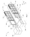
- FIG. 8 is a side perspective view of a chamber lid 612 spaced from the processing chamber 110 B.
- the lid 612 may be moved as shown by arrows “C” by disconnecting the vertical conduits 502 A, 502 E from the evacuation lines 224 , 226 at points 802 A, 802 B.
- the lid 612 may be moved without having to disassemble the entire evacuation system 700 or moving numerous, heavy system components.
- the lid 612 may be moved by sliding the lid 612 away from the processing chamber 110 B using a movement device such as a crane or hydraulic lifts.
- FIG. 9 illustrates the sequence for the robots 104 A, 104 B removing substrates 906 from the substrate stacking modules 102 A, 102 B and placing the substrates 906 into the substrate loading station environments 902 A- 902 D.
- the substrate loading stations 106 A, 106 B are shown to have two separate environments 902 A- 902 D. In each environment, the substrate carrier 906 faces a different direction. Thus, when the substrates 906 are disposed within the substrate loading station environments 902 A- 902 D, the substrates 906 are spaced apart by the carriers 904 within each separate substrate loading station 106 A, 106 B.
- Robot 104 A retrieves a substrate 906 from the substrate stacking module 102 A and moves along the track 202 to place the substrate 906 in either environment 902 B or 902 D.
- the substrate 906 is placed on a carrier 904 such that the substrate 906 faces the direction of arrow “E” away from the carrier 904 .
- robot 104 B retrieves a substrate 906 from the substrate stacking module 102 B and moves along the track 202 to place the substrate 906 in either environment 902 A, 902 C.
- both robots 104 A, 104 B can access the same substrate loading station 106 A, 106 B and move along the same track 202 .
- each robot 104 A, 104 B accesses a separate environment 902 A- 902 D of the substrate loading stations 106 A, 106 B and can only place the substrates 906 on respective carriers 904 facing a specific direction.
- FIGS. 10A-10C are schematic representations of the dual processing chambers 110 A, 110 B according to one embodiment.
- the dual processing chambers 110 A, 110 B include a plurality of microwave antennas 1010 disposed in a linear arrangement in the center of each processing chamber 110 A, 110 B.
- the antennas 1010 extend vertically from a top of the processing chamber to a bottom of the processing chamber.
- Each microwave antenna 1010 has a corresponding microwave power head 1012 at both the top and the bottom of the processing chamber that is coupled to the microwave antenna 1010 .
- the microwave power heads 1012 are staggered. The staggering may be due to space limitations. Power may be independently applied to the each end of the antenna 1010 through each power head 1012 .
- the microwave antennas 1010 may operate at a frequency within a range of 300 MHz and 300 GHz.
- Each of the processing chambers are arranged to be able to process two substrates, one on each side of the microwave antennas 1010 .
- the substrates are held in place within the processing chamber by a platen 1008 and a shadow frame 1004 .
- Gas introduction tubes may 1014 are disposed between adjacent microwave antennas 1010 .
- the gas introduction tubes 1014 extend vertically from the bottom to the top of the processing chamber parallel to the microwave antennas 1010 .
- the gas introduction tubes 1014 permit the introduction of processing gases, such as silicon precursors and nitrogen precursors. While not shown in FIGS. 10A-10C , the processing chambers 110 A, 110 B may be evacuated through a pumping port located behind the substrate carriers 1008 .
- FIGS. 11A and 11B are schematic representations of a processing chamber 1100 according to another embodiment.
- the processing chamber 1100 includes a plurality of plasma generators, such as microwave antennas, that extend vertically within the chamber body from a first end 1108 to a second end 1118 .
- the processing chamber 1100 includes a shadow frame 1104 on each side of the plasma generators 1102 for use in processing substrates.
- a shadow frame 1104 is disposed on opposite sides of the plurality of plasma generators 1102 so that there are two large area substrates may be processed within a single processing chamber 1100 and thus be exposed to the same processing environment either simultaneously or consecutively.
- Each plasma generator 1102 is coupled to a first waveguide 1110 at the first end 1108 thereof and to a second waveguide 1116 at the second end 1118 thereof.
- Each first waveguide 1110 is coupled to a first power source 1112 while each second waveguide is coupled to a second power source 1114 .
- the power sources 1112 , 1114 may be coupled to the waveguides 1110 , 1116 within an enclosure 1106 .
- the enclosures 1106 are staggered “T” shaped enclosures.
- the staggered “T” shaped enclosures may be necessary due to space limitations.
- adjacent waveguides 1110 , 1116 extend in opposite, parallel directions from the ends 1108 , 1118 to the respective power sources 1112 , 1114 .
- Gas introduction tubes may also be disposed within the processing chamber 1100 in the manner discussed above with regard to FIG. 10C .
- FIGS. 12A and 12B are schematic representations of a processing chamber 1200 according to another embodiment.
- the processing chamber 1200 includes a plurality of plasma generators, such as microwave antennas, that extend vertically within the chamber body from a first end 1208 to a second end 1218 .
- the processing chamber 1200 includes a shadow frame 1204 on each side of the plasma generators 1202 for use in processing substrates. As shown in FIG. 12B , a shadow frame 1204 is disposed on opposite sides of the plurality of plasma generators 1202 so that there are two large area substrates may be processed within a single processing chamber 1200 and thus be exposed to the same processing environment either simultaneously or consecutively.
- Each plasma generator 1202 is coupled to a first waveguide 1210 at the first end 1208 thereof and to a second waveguide 1216 at the second end 1218 thereof.
- Each first waveguide 1210 is coupled to a first power source 1212 while each second waveguide is coupled to a second power source 1214 .
- the power sources 1212 , 1214 may be coupled to the waveguides 1210 , 1216 within an enclosure 1206 .
- the enclosures 1206 all extend from the same side of the processing chamber 1200 .
- adjacent waveguides 1210 , 1216 extend in the same, parallel direction from the ends 1208 , 1218 to the respective power sources 1212 , 1214 .
- Gas introduction tubes may also be disposed within the processing chamber 1200 in the manner discussed above with regard to FIG. 10C .
- FIGS. 13A and 13B are schematic representations of a processing chamber 1300 according to another embodiment.
- the processing chamber 1300 includes a plurality of plasma generators, such as microwave antennas, that extend vertically within the chamber body from a first end 1308 to a second end 1318 .
- the processing chamber 1300 includes a shadow frame 1304 on each side of the plasma generators 1302 for use in processing substrates. As shown in FIG. 13B , a shadow frame 1304 is disposed on opposite sides of the plurality of plasma generators 1302 so that there are two large area substrates may be processed within a single processing chamber 1300 and thus be exposed to the same processing environment either simultaneously or consecutively.
- Each plasma generator 1302 is coupled to a first angled waveguide 1310 at the first end 1308 thereof and to a second angled waveguide 1316 at the second end 1318 thereof.
- Each first angled waveguide 1310 is coupled to a first power source 1312 while each second angled waveguide is coupled to a second power source 1314 .
- Enclosures 1306 are shown on top and bottom of the chamber 1300 by have been removed from the side of the chamber for clarity in viewing the waveguides 1310 , 1316 .
- the waveguides 1310 , 1316 extend along the top of the processing chamber 1300 and down along the side of the processing chamber 1300 to the respective power sources 1312 , 1314 .
- Gas introduction tubes may also be disposed within the processing chamber 1300 in the manner discussed above with regard to FIG. 10C .
- multiple substrates may be processed simultaneously. Processing multiple substrates simultaneously reduces the cost of manufacturing which may increase the manufacturer's profits.
Landscapes
- Chemical & Material Sciences (AREA)
- Engineering & Computer Science (AREA)
- Physics & Mathematics (AREA)
- Materials Engineering (AREA)
- General Physics & Mathematics (AREA)
- Mechanical Engineering (AREA)
- Metallurgy (AREA)
- Organic Chemistry (AREA)
- General Chemical & Material Sciences (AREA)
- Condensed Matter Physics & Semiconductors (AREA)
- Chemical Kinetics & Catalysis (AREA)
- Manufacturing & Machinery (AREA)
- Computer Hardware Design (AREA)
- Microelectronics & Electronic Packaging (AREA)
- Power Engineering (AREA)
- Plasma & Fusion (AREA)
- Analytical Chemistry (AREA)
- Chemical Vapour Deposition (AREA)
- Container, Conveyance, Adherence, Positioning, Of Wafer (AREA)
Priority Applications (1)
| Application Number | Priority Date | Filing Date | Title |
|---|---|---|---|
| US13/098,255 US9324597B2 (en) | 2010-04-30 | 2011-04-29 | Vertical inline CVD system |
Applications Claiming Priority (4)
| Application Number | Priority Date | Filing Date | Title |
|---|---|---|---|
| US33029610P | 2010-04-30 | 2010-04-30 | |
| US35423010P | 2010-06-13 | 2010-06-13 | |
| US41653210P | 2010-11-23 | 2010-11-23 | |
| US13/098,255 US9324597B2 (en) | 2010-04-30 | 2011-04-29 | Vertical inline CVD system |
Publications (2)
| Publication Number | Publication Date |
|---|---|
| US20120031335A1 US20120031335A1 (en) | 2012-02-09 |
| US9324597B2 true US9324597B2 (en) | 2016-04-26 |
Family
ID=44862144
Family Applications (2)
| Application Number | Title | Priority Date | Filing Date |
|---|---|---|---|
| US13/098,255 Expired - Fee Related US9324597B2 (en) | 2010-04-30 | 2011-04-29 | Vertical inline CVD system |
| US13/098,253 Expired - Fee Related US9922854B2 (en) | 2010-04-30 | 2011-04-29 | Vertical inline CVD system |
Family Applications After (1)
| Application Number | Title | Priority Date | Filing Date |
|---|---|---|---|
| US13/098,253 Expired - Fee Related US9922854B2 (en) | 2010-04-30 | 2011-04-29 | Vertical inline CVD system |
Country Status (6)
| Country | Link |
|---|---|
| US (2) | US9324597B2 (cg-RX-API-DMAC7.html) |
| JP (2) | JP2013527609A (cg-RX-API-DMAC7.html) |
| KR (2) | KR101932578B1 (cg-RX-API-DMAC7.html) |
| CN (2) | CN102859034B (cg-RX-API-DMAC7.html) |
| TW (2) | TWI544107B (cg-RX-API-DMAC7.html) |
| WO (2) | WO2011137373A2 (cg-RX-API-DMAC7.html) |
Families Citing this family (388)
| Publication number | Priority date | Publication date | Assignee | Title |
|---|---|---|---|---|
| US10378106B2 (en) | 2008-11-14 | 2019-08-13 | Asm Ip Holding B.V. | Method of forming insulation film by modified PEALD |
| US9394608B2 (en) | 2009-04-06 | 2016-07-19 | Asm America, Inc. | Semiconductor processing reactor and components thereof |
| US8802201B2 (en) | 2009-08-14 | 2014-08-12 | Asm America, Inc. | Systems and methods for thin-film deposition of metal oxides using excited nitrogen-oxygen species |
| US9324597B2 (en) * | 2010-04-30 | 2016-04-26 | Applied Materials, Inc. | Vertical inline CVD system |
| US9312155B2 (en) | 2011-06-06 | 2016-04-12 | Asm Japan K.K. | High-throughput semiconductor-processing apparatus equipped with multiple dual-chamber modules |
| US9048518B2 (en) | 2011-06-21 | 2015-06-02 | Applied Materials, Inc. | Transmission line RF applicator for plasma chamber |
| US10364496B2 (en) | 2011-06-27 | 2019-07-30 | Asm Ip Holding B.V. | Dual section module having shared and unshared mass flow controllers |
| US10854498B2 (en) | 2011-07-15 | 2020-12-01 | Asm Ip Holding B.V. | Wafer-supporting device and method for producing same |
| US20130023129A1 (en) | 2011-07-20 | 2013-01-24 | Asm America, Inc. | Pressure transmitter for a semiconductor processing environment |
| US9644268B2 (en) * | 2011-08-31 | 2017-05-09 | Alta Devices, Inc. | Thermal bridge for chemical vapor deposition reactors |
| US9017481B1 (en) | 2011-10-28 | 2015-04-28 | Asm America, Inc. | Process feed management for semiconductor substrate processing |
| WO2013112302A1 (en) * | 2012-01-27 | 2013-08-01 | Applied Materials, Inc. | Segmented antenna assembly |
| US20130206068A1 (en) * | 2012-02-13 | 2013-08-15 | Jozef Kudela | Linear pecvd apparatus |
| US9659799B2 (en) | 2012-08-28 | 2017-05-23 | Asm Ip Holding B.V. | Systems and methods for dynamic semiconductor process scheduling |
| US9021985B2 (en) | 2012-09-12 | 2015-05-05 | Asm Ip Holdings B.V. | Process gas management for an inductively-coupled plasma deposition reactor |
| US10714315B2 (en) | 2012-10-12 | 2020-07-14 | Asm Ip Holdings B.V. | Semiconductor reaction chamber showerhead |
| US20160376700A1 (en) | 2013-02-01 | 2016-12-29 | Asm Ip Holding B.V. | System for treatment of deposition reactor |
| US9484191B2 (en) | 2013-03-08 | 2016-11-01 | Asm Ip Holding B.V. | Pulsed remote plasma method and system |
| US9589770B2 (en) | 2013-03-08 | 2017-03-07 | Asm Ip Holding B.V. | Method and systems for in-situ formation of intermediate reactive species |
| US9240412B2 (en) | 2013-09-27 | 2016-01-19 | Asm Ip Holding B.V. | Semiconductor structure and device and methods of forming same using selective epitaxial process |
| TWI582028B (zh) * | 2014-01-03 | 2017-05-11 | 緯創資通股份有限公司 | 導引組裝料件系統及其導引料件台 |
| US10683571B2 (en) | 2014-02-25 | 2020-06-16 | Asm Ip Holding B.V. | Gas supply manifold and method of supplying gases to chamber using same |
| US10167557B2 (en) | 2014-03-18 | 2019-01-01 | Asm Ip Holding B.V. | Gas distribution system, reactor including the system, and methods of using the same |
| US11015245B2 (en) | 2014-03-19 | 2021-05-25 | Asm Ip Holding B.V. | Gas-phase reactor and system having exhaust plenum and components thereof |
| CN106165141B (zh) * | 2014-05-09 | 2019-01-15 | 应用材料公司 | 基板载体系统及使用它的方法 |
| WO2015171226A1 (en) * | 2014-05-09 | 2015-11-12 | Applied Materials, Inc. | Substrate carrier system with protective covering |
| US10858737B2 (en) | 2014-07-28 | 2020-12-08 | Asm Ip Holding B.V. | Showerhead assembly and components thereof |
| CN104195629A (zh) * | 2014-08-20 | 2014-12-10 | 中国科学院半导体研究所 | 塔式多片外延生长装置 |
| US9890456B2 (en) | 2014-08-21 | 2018-02-13 | Asm Ip Holding B.V. | Method and system for in situ formation of gas-phase compounds |
| US10941490B2 (en) | 2014-10-07 | 2021-03-09 | Asm Ip Holding B.V. | Multiple temperature range susceptor, assembly, reactor and system including the susceptor, and methods of using the same |
| US9657845B2 (en) | 2014-10-07 | 2017-05-23 | Asm Ip Holding B.V. | Variable conductance gas distribution apparatus and method |
| KR102263121B1 (ko) | 2014-12-22 | 2021-06-09 | 에이에스엠 아이피 홀딩 비.브이. | 반도체 소자 및 그 제조 방법 |
| US10529542B2 (en) | 2015-03-11 | 2020-01-07 | Asm Ip Holdings B.V. | Cross-flow reactor and method |
| US10276355B2 (en) | 2015-03-12 | 2019-04-30 | Asm Ip Holding B.V. | Multi-zone reactor, system including the reactor, and method of using the same |
| US10458018B2 (en) | 2015-06-26 | 2019-10-29 | Asm Ip Holding B.V. | Structures including metal carbide material, devices including the structures, and methods of forming same |
| US10600673B2 (en) * | 2015-07-07 | 2020-03-24 | Asm Ip Holding B.V. | Magnetic susceptor to baseplate seal |
| US10083836B2 (en) | 2015-07-24 | 2018-09-25 | Asm Ip Holding B.V. | Formation of boron-doped titanium metal films with high work function |
| KR102400863B1 (ko) * | 2015-07-27 | 2022-05-24 | 삼성디스플레이 주식회사 | 플라즈마 처리 장치 및 이를 이용하여 기판을 플라즈마 처리하는 방법 |
| US10039219B1 (en) | 2015-09-28 | 2018-07-31 | Western Digital Technologies, Inc. | Method and devices for picking and placing workpieces into devices under manufacture using dual robots |
| US9960072B2 (en) | 2015-09-29 | 2018-05-01 | Asm Ip Holding B.V. | Variable adjustment for precise matching of multiple chamber cavity housings |
| US10211308B2 (en) | 2015-10-21 | 2019-02-19 | Asm Ip Holding B.V. | NbMC layers |
| US10322384B2 (en) | 2015-11-09 | 2019-06-18 | Asm Ip Holding B.V. | Counter flow mixer for process chamber |
| US11139308B2 (en) | 2015-12-29 | 2021-10-05 | Asm Ip Holding B.V. | Atomic layer deposition of III-V compounds to form V-NAND devices |
| US10468251B2 (en) | 2016-02-19 | 2019-11-05 | Asm Ip Holding B.V. | Method for forming spacers using silicon nitride film for spacer-defined multiple patterning |
| US10529554B2 (en) | 2016-02-19 | 2020-01-07 | Asm Ip Holding B.V. | Method for forming silicon nitride film selectively on sidewalls or flat surfaces of trenches |
| US10501866B2 (en) | 2016-03-09 | 2019-12-10 | Asm Ip Holding B.V. | Gas distribution apparatus for improved film uniformity in an epitaxial system |
| US10343920B2 (en) | 2016-03-18 | 2019-07-09 | Asm Ip Holding B.V. | Aligned carbon nanotubes |
| US9892913B2 (en) | 2016-03-24 | 2018-02-13 | Asm Ip Holding B.V. | Radial and thickness control via biased multi-port injection settings |
| US10865475B2 (en) | 2016-04-21 | 2020-12-15 | Asm Ip Holding B.V. | Deposition of metal borides and silicides |
| US10190213B2 (en) | 2016-04-21 | 2019-01-29 | Asm Ip Holding B.V. | Deposition of metal borides |
| US10367080B2 (en) | 2016-05-02 | 2019-07-30 | Asm Ip Holding B.V. | Method of forming a germanium oxynitride film |
| US10032628B2 (en) | 2016-05-02 | 2018-07-24 | Asm Ip Holding B.V. | Source/drain performance through conformal solid state doping |
| KR102592471B1 (ko) | 2016-05-17 | 2023-10-20 | 에이에스엠 아이피 홀딩 비.브이. | 금속 배선 형성 방법 및 이를 이용한 반도체 장치의 제조 방법 |
| US11453943B2 (en) | 2016-05-25 | 2022-09-27 | Asm Ip Holding B.V. | Method for forming carbon-containing silicon/metal oxide or nitride film by ALD using silicon precursor and hydrocarbon precursor |
| US10388509B2 (en) | 2016-06-28 | 2019-08-20 | Asm Ip Holding B.V. | Formation of epitaxial layers via dislocation filtering |
| US10612137B2 (en) | 2016-07-08 | 2020-04-07 | Asm Ip Holdings B.V. | Organic reactants for atomic layer deposition |
| US9859151B1 (en) | 2016-07-08 | 2018-01-02 | Asm Ip Holding B.V. | Selective film deposition method to form air gaps |
| US10714385B2 (en) | 2016-07-19 | 2020-07-14 | Asm Ip Holding B.V. | Selective deposition of tungsten |
| KR102354490B1 (ko) | 2016-07-27 | 2022-01-21 | 에이에스엠 아이피 홀딩 비.브이. | 기판 처리 방법 |
| US9812320B1 (en) | 2016-07-28 | 2017-11-07 | Asm Ip Holding B.V. | Method and apparatus for filling a gap |
| US10395919B2 (en) | 2016-07-28 | 2019-08-27 | Asm Ip Holding B.V. | Method and apparatus for filling a gap |
| US9887082B1 (en) | 2016-07-28 | 2018-02-06 | Asm Ip Holding B.V. | Method and apparatus for filling a gap |
| KR102532607B1 (ko) | 2016-07-28 | 2023-05-15 | 에이에스엠 아이피 홀딩 비.브이. | 기판 가공 장치 및 그 동작 방법 |
| TWI588929B (zh) * | 2016-08-01 | 2017-06-21 | 矽品精密工業股份有限公司 | 承載設備及其操作方法 |
| US10410943B2 (en) | 2016-10-13 | 2019-09-10 | Asm Ip Holding B.V. | Method for passivating a surface of a semiconductor and related systems |
| US10643826B2 (en) | 2016-10-26 | 2020-05-05 | Asm Ip Holdings B.V. | Methods for thermally calibrating reaction chambers |
| US11532757B2 (en) | 2016-10-27 | 2022-12-20 | Asm Ip Holding B.V. | Deposition of charge trapping layers |
| US10643904B2 (en) | 2016-11-01 | 2020-05-05 | Asm Ip Holdings B.V. | Methods for forming a semiconductor device and related semiconductor device structures |
| US10229833B2 (en) | 2016-11-01 | 2019-03-12 | Asm Ip Holding B.V. | Methods for forming a transition metal nitride film on a substrate by atomic layer deposition and related semiconductor device structures |
| US10435790B2 (en) | 2016-11-01 | 2019-10-08 | Asm Ip Holding B.V. | Method of subatmospheric plasma-enhanced ALD using capacitively coupled electrodes with narrow gap |
| US10714350B2 (en) | 2016-11-01 | 2020-07-14 | ASM IP Holdings, B.V. | Methods for forming a transition metal niobium nitride film on a substrate by atomic layer deposition and related semiconductor device structures |
| US10134757B2 (en) | 2016-11-07 | 2018-11-20 | Asm Ip Holding B.V. | Method of processing a substrate and a device manufactured by using the method |
| KR102546317B1 (ko) | 2016-11-15 | 2023-06-21 | 에이에스엠 아이피 홀딩 비.브이. | 기체 공급 유닛 및 이를 포함하는 기판 처리 장치 |
| US10340135B2 (en) | 2016-11-28 | 2019-07-02 | Asm Ip Holding B.V. | Method of topologically restricted plasma-enhanced cyclic deposition of silicon or metal nitride |
| KR102762543B1 (ko) | 2016-12-14 | 2025-02-05 | 에이에스엠 아이피 홀딩 비.브이. | 기판 처리 장치 |
| US11581186B2 (en) | 2016-12-15 | 2023-02-14 | Asm Ip Holding B.V. | Sequential infiltration synthesis apparatus |
| US11447861B2 (en) | 2016-12-15 | 2022-09-20 | Asm Ip Holding B.V. | Sequential infiltration synthesis apparatus and a method of forming a patterned structure |
| KR102700194B1 (ko) | 2016-12-19 | 2024-08-28 | 에이에스엠 아이피 홀딩 비.브이. | 기판 처리 장치 |
| US10269558B2 (en) | 2016-12-22 | 2019-04-23 | Asm Ip Holding B.V. | Method of forming a structure on a substrate |
| US10867788B2 (en) | 2016-12-28 | 2020-12-15 | Asm Ip Holding B.V. | Method of forming a structure on a substrate |
| US11390950B2 (en) | 2017-01-10 | 2022-07-19 | Asm Ip Holding B.V. | Reactor system and method to reduce residue buildup during a film deposition process |
| US10655221B2 (en) | 2017-02-09 | 2020-05-19 | Asm Ip Holding B.V. | Method for depositing oxide film by thermal ALD and PEALD |
| US10468261B2 (en) | 2017-02-15 | 2019-11-05 | Asm Ip Holding B.V. | Methods for forming a metallic film on a substrate by cyclical deposition and related semiconductor device structures |
| US10529563B2 (en) | 2017-03-29 | 2020-01-07 | Asm Ip Holdings B.V. | Method for forming doped metal oxide films on a substrate by cyclical deposition and related semiconductor device structures |
| US10283353B2 (en) | 2017-03-29 | 2019-05-07 | Asm Ip Holding B.V. | Method of reforming insulating film deposited on substrate with recess pattern |
| KR102457289B1 (ko) | 2017-04-25 | 2022-10-21 | 에이에스엠 아이피 홀딩 비.브이. | 박막 증착 방법 및 반도체 장치의 제조 방법 |
| US10770286B2 (en) | 2017-05-08 | 2020-09-08 | Asm Ip Holdings B.V. | Methods for selectively forming a silicon nitride film on a substrate and related semiconductor device structures |
| US10892156B2 (en) | 2017-05-08 | 2021-01-12 | Asm Ip Holding B.V. | Methods for forming a silicon nitride film on a substrate and related semiconductor device structures |
| US10446393B2 (en) | 2017-05-08 | 2019-10-15 | Asm Ip Holding B.V. | Methods for forming silicon-containing epitaxial layers and related semiconductor device structures |
| US10504742B2 (en) | 2017-05-31 | 2019-12-10 | Asm Ip Holding B.V. | Method of atomic layer etching using hydrogen plasma |
| US10886123B2 (en) | 2017-06-02 | 2021-01-05 | Asm Ip Holding B.V. | Methods for forming low temperature semiconductor layers and related semiconductor device structures |
| US12040200B2 (en) | 2017-06-20 | 2024-07-16 | Asm Ip Holding B.V. | Semiconductor processing apparatus and methods for calibrating a semiconductor processing apparatus |
| US11306395B2 (en) | 2017-06-28 | 2022-04-19 | Asm Ip Holding B.V. | Methods for depositing a transition metal nitride film on a substrate by atomic layer deposition and related deposition apparatus |
| US10685834B2 (en) | 2017-07-05 | 2020-06-16 | Asm Ip Holdings B.V. | Methods for forming a silicon germanium tin layer and related semiconductor device structures |
| KR20190009245A (ko) | 2017-07-18 | 2019-01-28 | 에이에스엠 아이피 홀딩 비.브이. | 반도체 소자 구조물 형성 방법 및 관련된 반도체 소자 구조물 |
| US11374112B2 (en) | 2017-07-19 | 2022-06-28 | Asm Ip Holding B.V. | Method for depositing a group IV semiconductor and related semiconductor device structures |
| US11018002B2 (en) | 2017-07-19 | 2021-05-25 | Asm Ip Holding B.V. | Method for selectively depositing a Group IV semiconductor and related semiconductor device structures |
| US10541333B2 (en) | 2017-07-19 | 2020-01-21 | Asm Ip Holding B.V. | Method for depositing a group IV semiconductor and related semiconductor device structures |
| KR102069679B1 (ko) * | 2017-07-24 | 2020-01-23 | 어플라이드 머티어리얼스, 인코포레이티드 | 진공 챔버에서 기판을 프로세싱하기 위한 장치 및 시스템, 및 진공 챔버에서 캐리어를 운송하는 방법 |
| US10590535B2 (en) | 2017-07-26 | 2020-03-17 | Asm Ip Holdings B.V. | Chemical treatment, deposition and/or infiltration apparatus and method for using the same |
| US10605530B2 (en) | 2017-07-26 | 2020-03-31 | Asm Ip Holding B.V. | Assembly of a liner and a flange for a vertical furnace as well as the liner and the vertical furnace |
| US10312055B2 (en) | 2017-07-26 | 2019-06-04 | Asm Ip Holding B.V. | Method of depositing film by PEALD using negative bias |
| TWI815813B (zh) | 2017-08-04 | 2023-09-21 | 荷蘭商Asm智慧財產控股公司 | 用於分配反應腔內氣體的噴頭總成 |
| US10692741B2 (en) | 2017-08-08 | 2020-06-23 | Asm Ip Holdings B.V. | Radiation shield |
| US10770336B2 (en) | 2017-08-08 | 2020-09-08 | Asm Ip Holding B.V. | Substrate lift mechanism and reactor including same |
| US11769682B2 (en) | 2017-08-09 | 2023-09-26 | Asm Ip Holding B.V. | Storage apparatus for storing cassettes for substrates and processing apparatus equipped therewith |
| US11139191B2 (en) | 2017-08-09 | 2021-10-05 | Asm Ip Holding B.V. | Storage apparatus for storing cassettes for substrates and processing apparatus equipped therewith |
| US10249524B2 (en) | 2017-08-09 | 2019-04-02 | Asm Ip Holding B.V. | Cassette holder assembly for a substrate cassette and holding member for use in such assembly |
| US10236177B1 (en) | 2017-08-22 | 2019-03-19 | ASM IP Holding B.V.. | Methods for depositing a doped germanium tin semiconductor and related semiconductor device structures |
| USD900036S1 (en) | 2017-08-24 | 2020-10-27 | Asm Ip Holding B.V. | Heater electrical connector and adapter |
| US11830730B2 (en) | 2017-08-29 | 2023-11-28 | Asm Ip Holding B.V. | Layer forming method and apparatus |
| US11295980B2 (en) | 2017-08-30 | 2022-04-05 | Asm Ip Holding B.V. | Methods for depositing a molybdenum metal film over a dielectric surface of a substrate by a cyclical deposition process and related semiconductor device structures |
| KR102491945B1 (ko) | 2017-08-30 | 2023-01-26 | 에이에스엠 아이피 홀딩 비.브이. | 기판 처리 장치 |
| US11056344B2 (en) | 2017-08-30 | 2021-07-06 | Asm Ip Holding B.V. | Layer forming method |
| KR102401446B1 (ko) | 2017-08-31 | 2022-05-24 | 에이에스엠 아이피 홀딩 비.브이. | 기판 처리 장치 |
| US10607895B2 (en) | 2017-09-18 | 2020-03-31 | Asm Ip Holdings B.V. | Method for forming a semiconductor device structure comprising a gate fill metal |
| KR102630301B1 (ko) | 2017-09-21 | 2024-01-29 | 에이에스엠 아이피 홀딩 비.브이. | 침투성 재료의 순차 침투 합성 방법 처리 및 이를 이용하여 형성된 구조물 및 장치 |
| US10844484B2 (en) | 2017-09-22 | 2020-11-24 | Asm Ip Holding B.V. | Apparatus for dispensing a vapor phase reactant to a reaction chamber and related methods |
| US10658205B2 (en) | 2017-09-28 | 2020-05-19 | Asm Ip Holdings B.V. | Chemical dispensing apparatus and methods for dispensing a chemical to a reaction chamber |
| US10403504B2 (en) | 2017-10-05 | 2019-09-03 | Asm Ip Holding B.V. | Method for selectively depositing a metallic film on a substrate |
| US10319588B2 (en) | 2017-10-10 | 2019-06-11 | Asm Ip Holding B.V. | Method for depositing a metal chalcogenide on a substrate by cyclical deposition |
| US10861692B2 (en) * | 2017-10-26 | 2020-12-08 | Taiwan Semiconductor Manufacturing Co., Ltd. | Substrate carrier deterioration detection and repair |
| US10923344B2 (en) | 2017-10-30 | 2021-02-16 | Asm Ip Holding B.V. | Methods for forming a semiconductor structure and related semiconductor structures |
| KR102443047B1 (ko) | 2017-11-16 | 2022-09-14 | 에이에스엠 아이피 홀딩 비.브이. | 기판 처리 장치 방법 및 그에 의해 제조된 장치 |
| US10910262B2 (en) | 2017-11-16 | 2021-02-02 | Asm Ip Holding B.V. | Method of selectively depositing a capping layer structure on a semiconductor device structure |
| US11022879B2 (en) | 2017-11-24 | 2021-06-01 | Asm Ip Holding B.V. | Method of forming an enhanced unexposed photoresist layer |
| JP7206265B2 (ja) | 2017-11-27 | 2023-01-17 | エーエスエム アイピー ホールディング ビー.ブイ. | クリーン・ミニエンバイロメントを備える装置 |
| CN111316417B (zh) | 2017-11-27 | 2023-12-22 | 阿斯莫Ip控股公司 | 与批式炉偕同使用的用于储存晶圆匣的储存装置 |
| US10290508B1 (en) | 2017-12-05 | 2019-05-14 | Asm Ip Holding B.V. | Method for forming vertical spacers for spacer-defined patterning |
| CN108048818A (zh) * | 2017-12-18 | 2018-05-18 | 德淮半导体有限公司 | 化学气相沉积装置及其使用方法 |
| US10872771B2 (en) | 2018-01-16 | 2020-12-22 | Asm Ip Holding B. V. | Method for depositing a material film on a substrate within a reaction chamber by a cyclical deposition process and related device structures |
| CN111630203A (zh) | 2018-01-19 | 2020-09-04 | Asm Ip私人控股有限公司 | 通过等离子体辅助沉积来沉积间隙填充层的方法 |
| TWI852426B (zh) | 2018-01-19 | 2024-08-11 | 荷蘭商Asm Ip私人控股有限公司 | 沈積方法 |
| USD903477S1 (en) | 2018-01-24 | 2020-12-01 | Asm Ip Holdings B.V. | Metal clamp |
| US11018047B2 (en) | 2018-01-25 | 2021-05-25 | Asm Ip Holding B.V. | Hybrid lift pin |
| US10535516B2 (en) | 2018-02-01 | 2020-01-14 | Asm Ip Holdings B.V. | Method for depositing a semiconductor structure on a surface of a substrate and related semiconductor structures |
| USD880437S1 (en) | 2018-02-01 | 2020-04-07 | Asm Ip Holding B.V. | Gas supply plate for semiconductor manufacturing apparatus |
| US11081345B2 (en) | 2018-02-06 | 2021-08-03 | Asm Ip Holding B.V. | Method of post-deposition treatment for silicon oxide film |
| US10896820B2 (en) | 2018-02-14 | 2021-01-19 | Asm Ip Holding B.V. | Method for depositing a ruthenium-containing film on a substrate by a cyclical deposition process |
| JP7124098B2 (ja) | 2018-02-14 | 2022-08-23 | エーエスエム・アイピー・ホールディング・ベー・フェー | 周期的堆積プロセスにより基材上にルテニウム含有膜を堆積させる方法 |
| US10731249B2 (en) | 2018-02-15 | 2020-08-04 | Asm Ip Holding B.V. | Method of forming a transition metal containing film on a substrate by a cyclical deposition process, a method for supplying a transition metal halide compound to a reaction chamber, and related vapor deposition apparatus |
| US10658181B2 (en) | 2018-02-20 | 2020-05-19 | Asm Ip Holding B.V. | Method of spacer-defined direct patterning in semiconductor fabrication |
| KR102636427B1 (ko) | 2018-02-20 | 2024-02-13 | 에이에스엠 아이피 홀딩 비.브이. | 기판 처리 방법 및 장치 |
| US10975470B2 (en) | 2018-02-23 | 2021-04-13 | Asm Ip Holding B.V. | Apparatus for detecting or monitoring for a chemical precursor in a high temperature environment |
| TWI826925B (zh) | 2018-03-01 | 2023-12-21 | 美商應用材料股份有限公司 | 電漿源組件和氣體分配組件 |
| US12224156B2 (en) | 2018-03-01 | 2025-02-11 | Applied Materials, Inc. | Microwave plasma source for spatial plasma enhanced atomic layer deposition (PE-ALD) processing tool |
| US11473195B2 (en) | 2018-03-01 | 2022-10-18 | Asm Ip Holding B.V. | Semiconductor processing apparatus and a method for processing a substrate |
| US11629406B2 (en) | 2018-03-09 | 2023-04-18 | Asm Ip Holding B.V. | Semiconductor processing apparatus comprising one or more pyrometers for measuring a temperature of a substrate during transfer of the substrate |
| US11114283B2 (en) | 2018-03-16 | 2021-09-07 | Asm Ip Holding B.V. | Reactor, system including the reactor, and methods of manufacturing and using same |
| KR102646467B1 (ko) | 2018-03-27 | 2024-03-11 | 에이에스엠 아이피 홀딩 비.브이. | 기판 상에 전극을 형성하는 방법 및 전극을 포함하는 반도체 소자 구조 |
| US11088002B2 (en) | 2018-03-29 | 2021-08-10 | Asm Ip Holding B.V. | Substrate rack and a substrate processing system and method |
| US10510536B2 (en) | 2018-03-29 | 2019-12-17 | Asm Ip Holding B.V. | Method of depositing a co-doped polysilicon film on a surface of a substrate within a reaction chamber |
| US11230766B2 (en) | 2018-03-29 | 2022-01-25 | Asm Ip Holding B.V. | Substrate processing apparatus and method |
| KR102501472B1 (ko) | 2018-03-30 | 2023-02-20 | 에이에스엠 아이피 홀딩 비.브이. | 기판 처리 방법 |
| KR102600229B1 (ko) | 2018-04-09 | 2023-11-10 | 에이에스엠 아이피 홀딩 비.브이. | 기판 지지 장치, 이를 포함하는 기판 처리 장치 및 기판 처리 방법 |
| US12025484B2 (en) | 2018-05-08 | 2024-07-02 | Asm Ip Holding B.V. | Thin film forming method |
| TWI811348B (zh) | 2018-05-08 | 2023-08-11 | 荷蘭商Asm 智慧財產控股公司 | 藉由循環沉積製程於基板上沉積氧化物膜之方法及相關裝置結構 |
| US12272527B2 (en) | 2018-05-09 | 2025-04-08 | Asm Ip Holding B.V. | Apparatus for use with hydrogen radicals and method of using same |
| TWI879056B (zh) | 2018-05-11 | 2025-04-01 | 荷蘭商Asm Ip私人控股有限公司 | 用於基板上形成摻雜金屬碳化物薄膜之方法及相關半導體元件結構 |
| KR102596988B1 (ko) | 2018-05-28 | 2023-10-31 | 에이에스엠 아이피 홀딩 비.브이. | 기판 처리 방법 및 그에 의해 제조된 장치 |
| TWI840362B (zh) | 2018-06-04 | 2024-05-01 | 荷蘭商Asm Ip私人控股有限公司 | 水氣降低的晶圓處置腔室 |
| US11718913B2 (en) | 2018-06-04 | 2023-08-08 | Asm Ip Holding B.V. | Gas distribution system and reactor system including same |
| US11286562B2 (en) | 2018-06-08 | 2022-03-29 | Asm Ip Holding B.V. | Gas-phase chemical reactor and method of using same |
| KR102568797B1 (ko) | 2018-06-21 | 2023-08-21 | 에이에스엠 아이피 홀딩 비.브이. | 기판 처리 시스템 |
| US10797133B2 (en) | 2018-06-21 | 2020-10-06 | Asm Ip Holding B.V. | Method for depositing a phosphorus doped silicon arsenide film and related semiconductor device structures |
| JP7674105B2 (ja) | 2018-06-27 | 2025-05-09 | エーエスエム・アイピー・ホールディング・ベー・フェー | 金属含有材料ならびに金属含有材料を含む膜および構造体を形成するための周期的堆積方法 |
| CN112292477A (zh) | 2018-06-27 | 2021-01-29 | Asm Ip私人控股有限公司 | 用于形成含金属的材料的循环沉积方法及包含含金属的材料的膜和结构 |
| KR102686758B1 (ko) | 2018-06-29 | 2024-07-18 | 에이에스엠 아이피 홀딩 비.브이. | 박막 증착 방법 및 반도체 장치의 제조 방법 |
| US10612136B2 (en) | 2018-06-29 | 2020-04-07 | ASM IP Holding, B.V. | Temperature-controlled flange and reactor system including same |
| US10388513B1 (en) | 2018-07-03 | 2019-08-20 | Asm Ip Holding B.V. | Method for depositing silicon-free carbon-containing film as gap-fill layer by pulse plasma-assisted deposition |
| US10755922B2 (en) | 2018-07-03 | 2020-08-25 | Asm Ip Holding B.V. | Method for depositing silicon-free carbon-containing film as gap-fill layer by pulse plasma-assisted deposition |
| US10767789B2 (en) | 2018-07-16 | 2020-09-08 | Asm Ip Holding B.V. | Diaphragm valves, valve components, and methods for forming valve components |
| US10483099B1 (en) | 2018-07-26 | 2019-11-19 | Asm Ip Holding B.V. | Method for forming thermally stable organosilicon polymer film |
| US11053591B2 (en) | 2018-08-06 | 2021-07-06 | Asm Ip Holding B.V. | Multi-port gas injection system and reactor system including same |
| US10883175B2 (en) | 2018-08-09 | 2021-01-05 | Asm Ip Holding B.V. | Vertical furnace for processing substrates and a liner for use therein |
| US10829852B2 (en) | 2018-08-16 | 2020-11-10 | Asm Ip Holding B.V. | Gas distribution device for a wafer processing apparatus |
| US11430674B2 (en) | 2018-08-22 | 2022-08-30 | Asm Ip Holding B.V. | Sensor array, apparatus for dispensing a vapor phase reactant to a reaction chamber and related methods |
| KR102707956B1 (ko) | 2018-09-11 | 2024-09-19 | 에이에스엠 아이피 홀딩 비.브이. | 박막 증착 방법 |
| US11024523B2 (en) | 2018-09-11 | 2021-06-01 | Asm Ip Holding B.V. | Substrate processing apparatus and method |
| US11049751B2 (en) | 2018-09-14 | 2021-06-29 | Asm Ip Holding B.V. | Cassette supply system to store and handle cassettes and processing apparatus equipped therewith |
| CN110970344B (zh) | 2018-10-01 | 2024-10-25 | Asmip控股有限公司 | 衬底保持设备、包含所述设备的系统及其使用方法 |
| US11232963B2 (en) | 2018-10-03 | 2022-01-25 | Asm Ip Holding B.V. | Substrate processing apparatus and method |
| CN112840447B (zh) | 2018-10-04 | 2025-11-21 | 应用材料公司 | 运输系统 |
| KR102592699B1 (ko) | 2018-10-08 | 2023-10-23 | 에이에스엠 아이피 홀딩 비.브이. | 기판 지지 유닛 및 이를 포함하는 박막 증착 장치와 기판 처리 장치 |
| US10847365B2 (en) | 2018-10-11 | 2020-11-24 | Asm Ip Holding B.V. | Method of forming conformal silicon carbide film by cyclic CVD |
| US10811256B2 (en) | 2018-10-16 | 2020-10-20 | Asm Ip Holding B.V. | Method for etching a carbon-containing feature |
| KR102605121B1 (ko) | 2018-10-19 | 2023-11-23 | 에이에스엠 아이피 홀딩 비.브이. | 기판 처리 장치 및 기판 처리 방법 |
| KR102546322B1 (ko) | 2018-10-19 | 2023-06-21 | 에이에스엠 아이피 홀딩 비.브이. | 기판 처리 장치 및 기판 처리 방법 |
| USD948463S1 (en) | 2018-10-24 | 2022-04-12 | Asm Ip Holding B.V. | Susceptor for semiconductor substrate supporting apparatus |
| US10381219B1 (en) | 2018-10-25 | 2019-08-13 | Asm Ip Holding B.V. | Methods for forming a silicon nitride film |
| US12378665B2 (en) | 2018-10-26 | 2025-08-05 | Asm Ip Holding B.V. | High temperature coatings for a preclean and etch apparatus and related methods |
| US11145517B2 (en) * | 2018-10-29 | 2021-10-12 | Taiwan Semiconductor Manufacturing Co., Ltd. | Gas curtain for semiconductor manufacturing system |
| US11087997B2 (en) | 2018-10-31 | 2021-08-10 | Asm Ip Holding B.V. | Substrate processing apparatus for processing substrates |
| KR102748291B1 (ko) | 2018-11-02 | 2024-12-31 | 에이에스엠 아이피 홀딩 비.브이. | 기판 지지 유닛 및 이를 포함하는 기판 처리 장치 |
| US11572620B2 (en) | 2018-11-06 | 2023-02-07 | Asm Ip Holding B.V. | Methods for selectively depositing an amorphous silicon film on a substrate |
| US11031242B2 (en) | 2018-11-07 | 2021-06-08 | Asm Ip Holding B.V. | Methods for depositing a boron doped silicon germanium film |
| US10818758B2 (en) | 2018-11-16 | 2020-10-27 | Asm Ip Holding B.V. | Methods for forming a metal silicate film on a substrate in a reaction chamber and related semiconductor device structures |
| US10847366B2 (en) | 2018-11-16 | 2020-11-24 | Asm Ip Holding B.V. | Methods for depositing a transition metal chalcogenide film on a substrate by a cyclical deposition process |
| US10559458B1 (en) | 2018-11-26 | 2020-02-11 | Asm Ip Holding B.V. | Method of forming oxynitride film |
| US12040199B2 (en) | 2018-11-28 | 2024-07-16 | Asm Ip Holding B.V. | Substrate processing apparatus for processing substrates |
| US11217444B2 (en) | 2018-11-30 | 2022-01-04 | Asm Ip Holding B.V. | Method for forming an ultraviolet radiation responsive metal oxide-containing film |
| KR102636428B1 (ko) | 2018-12-04 | 2024-02-13 | 에이에스엠 아이피 홀딩 비.브이. | 기판 처리 장치를 세정하는 방법 |
| US11158513B2 (en) | 2018-12-13 | 2021-10-26 | Asm Ip Holding B.V. | Methods for forming a rhenium-containing film on a substrate by a cyclical deposition process and related semiconductor device structures |
| TWI874340B (zh) | 2018-12-14 | 2025-03-01 | 荷蘭商Asm Ip私人控股有限公司 | 形成裝置結構之方法、其所形成之結構及施行其之系統 |
| US11694913B2 (en) * | 2018-12-18 | 2023-07-04 | Intevac, Inc. | Hybrid system architecture for thin film deposition |
| TWI866480B (zh) | 2019-01-17 | 2024-12-11 | 荷蘭商Asm Ip 私人控股有限公司 | 藉由循環沈積製程於基板上形成含過渡金屬膜之方法 |
| KR102727227B1 (ko) | 2019-01-22 | 2024-11-07 | 에이에스엠 아이피 홀딩 비.브이. | 기판 처리 장치 |
| CN111524788B (zh) | 2019-02-01 | 2023-11-24 | Asm Ip私人控股有限公司 | 氧化硅的拓扑选择性膜形成的方法 |
| JP7509548B2 (ja) | 2019-02-20 | 2024-07-02 | エーエスエム・アイピー・ホールディング・ベー・フェー | 基材表面内に形成された凹部を充填するための周期的堆積方法および装置 |
| KR102626263B1 (ko) | 2019-02-20 | 2024-01-16 | 에이에스엠 아이피 홀딩 비.브이. | 처리 단계를 포함하는 주기적 증착 방법 및 이를 위한 장치 |
| KR102638425B1 (ko) | 2019-02-20 | 2024-02-21 | 에이에스엠 아이피 홀딩 비.브이. | 기판 표면 내에 형성된 오목부를 충진하기 위한 방법 및 장치 |
| US11482533B2 (en) | 2019-02-20 | 2022-10-25 | Asm Ip Holding B.V. | Apparatus and methods for plug fill deposition in 3-D NAND applications |
| TWI842826B (zh) | 2019-02-22 | 2024-05-21 | 荷蘭商Asm Ip私人控股有限公司 | 基材處理設備及處理基材之方法 |
| KR102548322B1 (ko) * | 2019-02-28 | 2023-06-28 | 도시바 미쓰비시덴키 산교시스템 가부시키가이샤 | 성막 장치 |
| US11742198B2 (en) | 2019-03-08 | 2023-08-29 | Asm Ip Holding B.V. | Structure including SiOCN layer and method of forming same |
| KR102782593B1 (ko) | 2019-03-08 | 2025-03-14 | 에이에스엠 아이피 홀딩 비.브이. | SiOC 층을 포함한 구조체 및 이의 형성 방법 |
| KR102858005B1 (ko) | 2019-03-08 | 2025-09-09 | 에이에스엠 아이피 홀딩 비.브이. | 실리콘 질화물 층을 선택적으로 증착하는 방법, 및 선택적으로 증착된 실리콘 질화물 층을 포함하는 구조체 |
| KR20200116033A (ko) | 2019-03-28 | 2020-10-08 | 에이에스엠 아이피 홀딩 비.브이. | 도어 개방기 및 이를 구비한 기판 처리 장치 |
| KR102809999B1 (ko) | 2019-04-01 | 2025-05-19 | 에이에스엠 아이피 홀딩 비.브이. | 반도체 소자를 제조하는 방법 |
| US11447864B2 (en) | 2019-04-19 | 2022-09-20 | Asm Ip Holding B.V. | Layer forming method and apparatus |
| KR20200125453A (ko) | 2019-04-24 | 2020-11-04 | 에이에스엠 아이피 홀딩 비.브이. | 기상 반응기 시스템 및 이를 사용하는 방법 |
| KR20200130121A (ko) | 2019-05-07 | 2020-11-18 | 에이에스엠 아이피 홀딩 비.브이. | 딥 튜브가 있는 화학물질 공급원 용기 |
| KR102869364B1 (ko) | 2019-05-07 | 2025-10-10 | 에이에스엠 아이피 홀딩 비.브이. | 비정질 탄소 중합체 막을 개질하는 방법 |
| KR20200130652A (ko) | 2019-05-10 | 2020-11-19 | 에이에스엠 아이피 홀딩 비.브이. | 표면 상에 재료를 증착하는 방법 및 본 방법에 따라 형성된 구조 |
| JP7598201B2 (ja) | 2019-05-16 | 2024-12-11 | エーエスエム・アイピー・ホールディング・ベー・フェー | ウェハボートハンドリング装置、縦型バッチ炉および方法 |
| JP7612342B2 (ja) | 2019-05-16 | 2025-01-14 | エーエスエム・アイピー・ホールディング・ベー・フェー | ウェハボートハンドリング装置、縦型バッチ炉および方法 |
| USD947913S1 (en) | 2019-05-17 | 2022-04-05 | Asm Ip Holding B.V. | Susceptor shaft |
| USD975665S1 (en) | 2019-05-17 | 2023-01-17 | Asm Ip Holding B.V. | Susceptor shaft |
| US11538706B2 (en) | 2019-05-24 | 2022-12-27 | Applied Materials, Inc. | System and method for aligning a mask with a substrate |
| USD935572S1 (en) | 2019-05-24 | 2021-11-09 | Asm Ip Holding B.V. | Gas channel plate |
| US11189516B2 (en) | 2019-05-24 | 2021-11-30 | Applied Materials, Inc. | Method for mask and substrate alignment |
| USD922229S1 (en) | 2019-06-05 | 2021-06-15 | Asm Ip Holding B.V. | Device for controlling a temperature of a gas supply unit |
| KR20200141003A (ko) | 2019-06-06 | 2020-12-17 | 에이에스엠 아이피 홀딩 비.브이. | 가스 감지기를 포함하는 기상 반응기 시스템 |
| KR20200141931A (ko) | 2019-06-10 | 2020-12-21 | 에이에스엠 아이피 홀딩 비.브이. | 석영 에피택셜 챔버를 세정하는 방법 |
| KR20200143254A (ko) | 2019-06-11 | 2020-12-23 | 에이에스엠 아이피 홀딩 비.브이. | 개질 가스를 사용하여 전자 구조를 형성하는 방법, 상기 방법을 수행하기 위한 시스템, 및 상기 방법을 사용하여 형성되는 구조 |
| USD944946S1 (en) | 2019-06-14 | 2022-03-01 | Asm Ip Holding B.V. | Shower plate |
| USD931978S1 (en) | 2019-06-27 | 2021-09-28 | Asm Ip Holding B.V. | Showerhead vacuum transport |
| KR20210005515A (ko) | 2019-07-03 | 2021-01-14 | 에이에스엠 아이피 홀딩 비.브이. | 기판 처리 장치용 온도 제어 조립체 및 이를 사용하는 방법 |
| JP7499079B2 (ja) | 2019-07-09 | 2024-06-13 | エーエスエム・アイピー・ホールディング・ベー・フェー | 同軸導波管を用いたプラズマ装置、基板処理方法 |
| CN112216646A (zh) | 2019-07-10 | 2021-01-12 | Asm Ip私人控股有限公司 | 基板支撑组件及包括其的基板处理装置 |
| KR102895115B1 (ko) | 2019-07-16 | 2025-12-03 | 에이에스엠 아이피 홀딩 비.브이. | 기판 처리 장치 |
| KR102860110B1 (ko) | 2019-07-17 | 2025-09-16 | 에이에스엠 아이피 홀딩 비.브이. | 실리콘 게르마늄 구조를 형성하는 방법 |
| KR20210010816A (ko) | 2019-07-17 | 2021-01-28 | 에이에스엠 아이피 홀딩 비.브이. | 라디칼 보조 점화 플라즈마 시스템 및 방법 |
| CN110331378B (zh) * | 2019-07-18 | 2024-01-19 | 中国科学院金属研究所 | 金刚石薄膜连续制备使用的hfcvd设备及其镀膜方法 |
| US11643724B2 (en) | 2019-07-18 | 2023-05-09 | Asm Ip Holding B.V. | Method of forming structures using a neutral beam |
| TWI839544B (zh) | 2019-07-19 | 2024-04-21 | 荷蘭商Asm Ip私人控股有限公司 | 形成形貌受控的非晶碳聚合物膜之方法 |
| CN112242295B (zh) | 2019-07-19 | 2025-12-09 | Asmip私人控股有限公司 | 形成拓扑受控的无定形碳聚合物膜的方法 |
| US11756816B2 (en) | 2019-07-26 | 2023-09-12 | Applied Materials, Inc. | Carrier FOUP and a method of placing a carrier |
| US10916464B1 (en) | 2019-07-26 | 2021-02-09 | Applied Materials, Inc. | Method of pre aligning carrier, wafer and carrier-wafer combination for throughput efficiency |
| US11196360B2 (en) | 2019-07-26 | 2021-12-07 | Applied Materials, Inc. | System and method for electrostatically chucking a substrate to a carrier |
| TWI851767B (zh) | 2019-07-29 | 2024-08-11 | 荷蘭商Asm Ip私人控股有限公司 | 用於利用n型摻雜物及/或替代摻雜物選擇性沉積以達成高摻雜物併入之方法 |
| CN112309900B (zh) | 2019-07-30 | 2025-11-04 | Asmip私人控股有限公司 | 基板处理设备 |
| CN112309899B (zh) | 2019-07-30 | 2025-11-14 | Asmip私人控股有限公司 | 基板处理设备 |
| KR20210015655A (ko) | 2019-07-30 | 2021-02-10 | 에이에스엠 아이피 홀딩 비.브이. | 기판 처리 장치 및 방법 |
| US11227782B2 (en) | 2019-07-31 | 2022-01-18 | Asm Ip Holding B.V. | Vertical batch furnace assembly |
| US11587814B2 (en) | 2019-07-31 | 2023-02-21 | Asm Ip Holding B.V. | Vertical batch furnace assembly |
| US11587815B2 (en) | 2019-07-31 | 2023-02-21 | Asm Ip Holding B.V. | Vertical batch furnace assembly |
| CN118422165A (zh) | 2019-08-05 | 2024-08-02 | Asm Ip私人控股有限公司 | 用于化学源容器的液位传感器 |
| KR20210018761A (ko) | 2019-08-09 | 2021-02-18 | 에이에스엠 아이피 홀딩 비.브이. | 냉각 장치를 포함한 히터 어셈블리 및 이를 사용하는 방법 |
| USD965524S1 (en) | 2019-08-19 | 2022-10-04 | Asm Ip Holding B.V. | Susceptor support |
| USD965044S1 (en) | 2019-08-19 | 2022-09-27 | Asm Ip Holding B.V. | Susceptor shaft |
| JP2021031769A (ja) | 2019-08-21 | 2021-03-01 | エーエスエム アイピー ホールディング ビー.ブイ. | 成膜原料混合ガス生成装置及び成膜装置 |
| USD940837S1 (en) | 2019-08-22 | 2022-01-11 | Asm Ip Holding B.V. | Electrode |
| USD949319S1 (en) | 2019-08-22 | 2022-04-19 | Asm Ip Holding B.V. | Exhaust duct |
| USD930782S1 (en) | 2019-08-22 | 2021-09-14 | Asm Ip Holding B.V. | Gas distributor |
| USD979506S1 (en) | 2019-08-22 | 2023-02-28 | Asm Ip Holding B.V. | Insulator |
| KR20210024423A (ko) | 2019-08-22 | 2021-03-05 | 에이에스엠 아이피 홀딩 비.브이. | 홀을 구비한 구조체를 형성하기 위한 방법 |
| US11286558B2 (en) | 2019-08-23 | 2022-03-29 | Asm Ip Holding B.V. | Methods for depositing a molybdenum nitride film on a surface of a substrate by a cyclical deposition process and related semiconductor device structures including a molybdenum nitride film |
| KR20210024420A (ko) | 2019-08-23 | 2021-03-05 | 에이에스엠 아이피 홀딩 비.브이. | 비스(디에틸아미노)실란을 사용하여 peald에 의해 개선된 품질을 갖는 실리콘 산화물 막을 증착하기 위한 방법 |
| KR102806450B1 (ko) | 2019-09-04 | 2025-05-12 | 에이에스엠 아이피 홀딩 비.브이. | 희생 캡핑 층을 이용한 선택적 증착 방법 |
| KR102733104B1 (ko) | 2019-09-05 | 2024-11-22 | 에이에스엠 아이피 홀딩 비.브이. | 기판 처리 장치 |
| US12469693B2 (en) | 2019-09-17 | 2025-11-11 | Asm Ip Holding B.V. | Method of forming a carbon-containing layer and structure including the layer |
| US11562901B2 (en) | 2019-09-25 | 2023-01-24 | Asm Ip Holding B.V. | Substrate processing method |
| CN112593212B (zh) | 2019-10-02 | 2023-12-22 | Asm Ip私人控股有限公司 | 通过循环等离子体增强沉积工艺形成拓扑选择性氧化硅膜的方法 |
| KR20210042810A (ko) | 2019-10-08 | 2021-04-20 | 에이에스엠 아이피 홀딩 비.브이. | 활성 종을 이용하기 위한 가스 분배 어셈블리를 포함한 반응기 시스템 및 이를 사용하는 방법 |
| TW202128273A (zh) | 2019-10-08 | 2021-08-01 | 荷蘭商Asm Ip私人控股有限公司 | 氣體注入系統、及將材料沉積於反應室內之基板表面上的方法 |
| TWI846953B (zh) | 2019-10-08 | 2024-07-01 | 荷蘭商Asm Ip私人控股有限公司 | 基板處理裝置 |
| KR102879443B1 (ko) | 2019-10-10 | 2025-11-03 | 에이에스엠 아이피 홀딩 비.브이. | 포토레지스트 하부층을 형성하기 위한 방법 및 이를 포함한 구조체 |
| US12009241B2 (en) | 2019-10-14 | 2024-06-11 | Asm Ip Holding B.V. | Vertical batch furnace assembly with detector to detect cassette |
| TWI834919B (zh) | 2019-10-16 | 2024-03-11 | 荷蘭商Asm Ip私人控股有限公司 | 氧化矽之拓撲選擇性膜形成之方法 |
| US11637014B2 (en) | 2019-10-17 | 2023-04-25 | Asm Ip Holding B.V. | Methods for selective deposition of doped semiconductor material |
| KR102845724B1 (ko) | 2019-10-21 | 2025-08-13 | 에이에스엠 아이피 홀딩 비.브이. | 막을 선택적으로 에칭하기 위한 장치 및 방법 |
| KR20210050453A (ko) | 2019-10-25 | 2021-05-07 | 에이에스엠 아이피 홀딩 비.브이. | 기판 표면 상의 갭 피처를 충진하는 방법 및 이와 관련된 반도체 소자 구조 |
| US11646205B2 (en) | 2019-10-29 | 2023-05-09 | Asm Ip Holding B.V. | Methods of selectively forming n-type doped material on a surface, systems for selectively forming n-type doped material, and structures formed using same |
| KR102890638B1 (ko) | 2019-11-05 | 2025-11-25 | 에이에스엠 아이피 홀딩 비.브이. | 도핑된 반도체 층을 갖는 구조체 및 이를 형성하기 위한 방법 및 시스템 |
| US11501968B2 (en) | 2019-11-15 | 2022-11-15 | Asm Ip Holding B.V. | Method for providing a semiconductor device with silicon filled gaps |
| KR102861314B1 (ko) | 2019-11-20 | 2025-09-17 | 에이에스엠 아이피 홀딩 비.브이. | 기판의 표면 상에 탄소 함유 물질을 증착하는 방법, 상기 방법을 사용하여 형성된 구조물, 및 상기 구조물을 형성하기 위한 시스템 |
| CN112951697B (zh) | 2019-11-26 | 2025-07-29 | Asmip私人控股有限公司 | 基板处理设备 |
| US11450529B2 (en) | 2019-11-26 | 2022-09-20 | Asm Ip Holding B.V. | Methods for selectively forming a target film on a substrate comprising a first dielectric surface and a second metallic surface |
| CN120998766A (zh) | 2019-11-29 | 2025-11-21 | Asm Ip私人控股有限公司 | 基板处理设备 |
| CN120432376A (zh) | 2019-11-29 | 2025-08-05 | Asm Ip私人控股有限公司 | 基板处理设备 |
| JP7527928B2 (ja) | 2019-12-02 | 2024-08-05 | エーエスエム・アイピー・ホールディング・ベー・フェー | 基板処理装置、基板処理方法 |
| KR20210070898A (ko) | 2019-12-04 | 2021-06-15 | 에이에스엠 아이피 홀딩 비.브이. | 기판 처리 장치 |
| US11885013B2 (en) | 2019-12-17 | 2024-01-30 | Asm Ip Holding B.V. | Method of forming vanadium nitride layer and structure including the vanadium nitride layer |
| US11527403B2 (en) | 2019-12-19 | 2022-12-13 | Asm Ip Holding B.V. | Methods for filling a gap feature on a substrate surface and related semiconductor structures |
| JP7730637B2 (ja) | 2020-01-06 | 2025-08-28 | エーエスエム・アイピー・ホールディング・ベー・フェー | ガス供給アセンブリ、その構成要素、およびこれを含む反応器システム |
| KR20210089079A (ko) | 2020-01-06 | 2021-07-15 | 에이에스엠 아이피 홀딩 비.브이. | 채널형 리프트 핀 |
| DE102020100171B3 (de) * | 2020-01-07 | 2021-07-01 | Cemecon Ag | Vorrichtung zum Halten von Werkstücken, Beschichtungsanlage sowie Verfahren zum Beschichten eines Werkstücks |
| US11993847B2 (en) | 2020-01-08 | 2024-05-28 | Asm Ip Holding B.V. | Injector |
| KR102882467B1 (ko) | 2020-01-16 | 2025-11-05 | 에이에스엠 아이피 홀딩 비.브이. | 고 종횡비 피처를 형성하는 방법 |
| KR102675856B1 (ko) | 2020-01-20 | 2024-06-17 | 에이에스엠 아이피 홀딩 비.브이. | 박막 형성 방법 및 박막 표면 개질 방법 |
| CN115516657A (zh) | 2020-01-22 | 2022-12-23 | 应用材料公司 | Oled层厚度和掺杂剂浓度的产线内监测 |
| EP4094306A4 (en) | 2020-01-22 | 2024-02-28 | Applied Materials, Inc. | ONLINE MONITORING OF OLED LAYER THICKNESS AND DOPANT CONCENTRATION |
| TWI889744B (zh) | 2020-01-29 | 2025-07-11 | 荷蘭商Asm Ip私人控股有限公司 | 污染物捕集系統、及擋板堆疊 |
| TW202513845A (zh) | 2020-02-03 | 2025-04-01 | 荷蘭商Asm Ip私人控股有限公司 | 半導體裝置結構及其形成方法 |
| KR20210100010A (ko) | 2020-02-04 | 2021-08-13 | 에이에스엠 아이피 홀딩 비.브이. | 대형 물품의 투과율 측정을 위한 방법 및 장치 |
| US11776846B2 (en) | 2020-02-07 | 2023-10-03 | Asm Ip Holding B.V. | Methods for depositing gap filling fluids and related systems and devices |
| KR20210103956A (ko) | 2020-02-13 | 2021-08-24 | 에이에스엠 아이피 홀딩 비.브이. | 수광 장치를 포함하는 기판 처리 장치 및 수광 장치의 교정 방법 |
| TW202146691A (zh) | 2020-02-13 | 2021-12-16 | 荷蘭商Asm Ip私人控股有限公司 | 氣體分配總成、噴淋板總成、及調整至反應室之氣體的傳導率之方法 |
| TWI855223B (zh) | 2020-02-17 | 2024-09-11 | 荷蘭商Asm Ip私人控股有限公司 | 用於生長磷摻雜矽層之方法 |
| TWI895326B (zh) | 2020-02-28 | 2025-09-01 | 荷蘭商Asm Ip私人控股有限公司 | 專用於零件清潔的系統 |
| TW202139347A (zh) | 2020-03-04 | 2021-10-16 | 荷蘭商Asm Ip私人控股有限公司 | 反應器系統、對準夾具、及對準方法 |
| US11876356B2 (en) | 2020-03-11 | 2024-01-16 | Asm Ip Holding B.V. | Lockout tagout assembly and system and method of using same |
| KR20210116240A (ko) | 2020-03-11 | 2021-09-27 | 에이에스엠 아이피 홀딩 비.브이. | 조절성 접합부를 갖는 기판 핸들링 장치 |
| CN113394086A (zh) | 2020-03-12 | 2021-09-14 | Asm Ip私人控股有限公司 | 用于制造具有目标拓扑轮廓的层结构的方法 |
| US12173404B2 (en) | 2020-03-17 | 2024-12-24 | Asm Ip Holding B.V. | Method of depositing epitaxial material, structure formed using the method, and system for performing the method |
| KR102755229B1 (ko) | 2020-04-02 | 2025-01-14 | 에이에스엠 아이피 홀딩 비.브이. | 박막 형성 방법 |
| TWI887376B (zh) | 2020-04-03 | 2025-06-21 | 荷蘭商Asm Ip私人控股有限公司 | 半導體裝置的製造方法 |
| TWI888525B (zh) | 2020-04-08 | 2025-07-01 | 荷蘭商Asm Ip私人控股有限公司 | 用於選擇性蝕刻氧化矽膜之設備及方法 |
| US11821078B2 (en) | 2020-04-15 | 2023-11-21 | Asm Ip Holding B.V. | Method for forming precoat film and method for forming silicon-containing film |
| KR20210128343A (ko) | 2020-04-15 | 2021-10-26 | 에이에스엠 아이피 홀딩 비.브이. | 크롬 나이트라이드 층을 형성하는 방법 및 크롬 나이트라이드 층을 포함하는 구조 |
| US11996289B2 (en) | 2020-04-16 | 2024-05-28 | Asm Ip Holding B.V. | Methods of forming structures including silicon germanium and silicon layers, devices formed using the methods, and systems for performing the methods |
| TW202143328A (zh) | 2020-04-21 | 2021-11-16 | 荷蘭商Asm Ip私人控股有限公司 | 用於調整膜應力之方法 |
| TWI887400B (zh) | 2020-04-24 | 2025-06-21 | 荷蘭商Asm Ip私人控股有限公司 | 用於穩定釩化合物之方法及設備 |
| TW202208671A (zh) | 2020-04-24 | 2022-03-01 | 荷蘭商Asm Ip私人控股有限公司 | 形成包括硼化釩及磷化釩層的結構之方法 |
| US11898243B2 (en) | 2020-04-24 | 2024-02-13 | Asm Ip Holding B.V. | Method of forming vanadium nitride-containing layer |
| KR20210132600A (ko) | 2020-04-24 | 2021-11-04 | 에이에스엠 아이피 홀딩 비.브이. | 바나듐, 질소 및 추가 원소를 포함한 층을 증착하기 위한 방법 및 시스템 |
| TW202146831A (zh) | 2020-04-24 | 2021-12-16 | 荷蘭商Asm Ip私人控股有限公司 | 垂直批式熔爐總成、及用於冷卻垂直批式熔爐之方法 |
| KR102783898B1 (ko) | 2020-04-29 | 2025-03-18 | 에이에스엠 아이피 홀딩 비.브이. | 고체 소스 전구체 용기 |
| KR20210134869A (ko) | 2020-05-01 | 2021-11-11 | 에이에스엠 아이피 홀딩 비.브이. | Foup 핸들러를 이용한 foup의 빠른 교환 |
| JP7726664B2 (ja) | 2020-05-04 | 2025-08-20 | エーエスエム・アイピー・ホールディング・ベー・フェー | 基板を処理するための基板処理システム |
| JP7736446B2 (ja) | 2020-05-07 | 2025-09-09 | エーエスエム・アイピー・ホールディング・ベー・フェー | 同調回路を備える反応器システム |
| KR102788543B1 (ko) | 2020-05-13 | 2025-03-27 | 에이에스엠 아이피 홀딩 비.브이. | 반응기 시스템용 레이저 정렬 고정구 |
| TW202146699A (zh) | 2020-05-15 | 2021-12-16 | 荷蘭商Asm Ip私人控股有限公司 | 形成矽鍺層之方法、半導體結構、半導體裝置、形成沉積層之方法、及沉積系統 |
| TW202147383A (zh) | 2020-05-19 | 2021-12-16 | 荷蘭商Asm Ip私人控股有限公司 | 基材處理設備 |
| KR102795476B1 (ko) | 2020-05-21 | 2025-04-11 | 에이에스엠 아이피 홀딩 비.브이. | 다수의 탄소 층을 포함한 구조체 및 이를 형성하고 사용하는 방법 |
| KR20210145079A (ko) | 2020-05-21 | 2021-12-01 | 에이에스엠 아이피 홀딩 비.브이. | 기판을 처리하기 위한 플랜지 및 장치 |
| KR102702526B1 (ko) | 2020-05-22 | 2024-09-03 | 에이에스엠 아이피 홀딩 비.브이. | 과산화수소를 사용하여 박막을 증착하기 위한 장치 |
| KR20210146802A (ko) | 2020-05-26 | 2021-12-06 | 에이에스엠 아이피 홀딩 비.브이. | 붕소 및 갈륨을 함유한 실리콘 게르마늄 층을 증착하는 방법 |
| TWI876048B (zh) | 2020-05-29 | 2025-03-11 | 荷蘭商Asm Ip私人控股有限公司 | 基板處理方法 |
| TW202212620A (zh) | 2020-06-02 | 2022-04-01 | 荷蘭商Asm Ip私人控股有限公司 | 處理基板之設備、形成膜之方法、及控制用於處理基板之設備之方法 |
| CN113774363A (zh) * | 2020-06-09 | 2021-12-10 | 江苏菲沃泰纳米科技股份有限公司 | 镀膜设备及其镀膜方法 |
| KR20210156219A (ko) | 2020-06-16 | 2021-12-24 | 에이에스엠 아이피 홀딩 비.브이. | 붕소를 함유한 실리콘 게르마늄 층을 증착하는 방법 |
| JP7703376B2 (ja) | 2020-06-24 | 2025-07-07 | エーエスエム・アイピー・ホールディング・ベー・フェー | シリコンを備える層を形成するための方法 |
| TWI873359B (zh) | 2020-06-30 | 2025-02-21 | 荷蘭商Asm Ip私人控股有限公司 | 基板處理方法 |
| US12431354B2 (en) | 2020-07-01 | 2025-09-30 | Asm Ip Holding B.V. | Silicon nitride and silicon oxide deposition methods using fluorine inhibitor |
| KR102707957B1 (ko) | 2020-07-08 | 2024-09-19 | 에이에스엠 아이피 홀딩 비.브이. | 기판 처리 방법 |
| US11521870B2 (en) * | 2020-07-08 | 2022-12-06 | Applied Materials, Inc. | Annealing chamber |
| TWI864307B (zh) | 2020-07-17 | 2024-12-01 | 荷蘭商Asm Ip私人控股有限公司 | 用於光微影之結構、方法與系統 |
| TWI878570B (zh) | 2020-07-20 | 2025-04-01 | 荷蘭商Asm Ip私人控股有限公司 | 用於沉積鉬層之方法及系統 |
| KR20220011092A (ko) | 2020-07-20 | 2022-01-27 | 에이에스엠 아이피 홀딩 비.브이. | 전이 금속층을 포함하는 구조체를 형성하기 위한 방법 및 시스템 |
| US12322591B2 (en) | 2020-07-27 | 2025-06-03 | Asm Ip Holding B.V. | Thin film deposition process |
| KR20220021863A (ko) | 2020-08-14 | 2022-02-22 | 에이에스엠 아이피 홀딩 비.브이. | 기판 처리 방법 |
| US12040177B2 (en) | 2020-08-18 | 2024-07-16 | Asm Ip Holding B.V. | Methods for forming a laminate film by cyclical plasma-enhanced deposition processes |
| TW202228863A (zh) | 2020-08-25 | 2022-08-01 | 荷蘭商Asm Ip私人控股有限公司 | 清潔基板的方法、選擇性沉積的方法、及反應器系統 |
| US11725280B2 (en) | 2020-08-26 | 2023-08-15 | Asm Ip Holding B.V. | Method for forming metal silicon oxide and metal silicon oxynitride layers |
| TW202229601A (zh) | 2020-08-27 | 2022-08-01 | 荷蘭商Asm Ip私人控股有限公司 | 形成圖案化結構的方法、操控機械特性的方法、裝置結構、及基板處理系統 |
| KR20220033997A (ko) | 2020-09-10 | 2022-03-17 | 에이에스엠 아이피 홀딩 비.브이. | 갭 충진 유체를 증착하기 위한 방법 그리고 이와 관련된 시스템 및 장치 |
| USD990534S1 (en) | 2020-09-11 | 2023-06-27 | Asm Ip Holding B.V. | Weighted lift pin |
| KR20220036866A (ko) | 2020-09-16 | 2022-03-23 | 에이에스엠 아이피 홀딩 비.브이. | 실리콘 산화물 증착 방법 |
| USD1012873S1 (en) | 2020-09-24 | 2024-01-30 | Asm Ip Holding B.V. | Electrode for semiconductor processing apparatus |
| TWI889903B (zh) | 2020-09-25 | 2025-07-11 | 荷蘭商Asm Ip私人控股有限公司 | 基板處理方法 |
| US12009224B2 (en) | 2020-09-29 | 2024-06-11 | Asm Ip Holding B.V. | Apparatus and method for etching metal nitrides |
| KR20220045900A (ko) | 2020-10-06 | 2022-04-13 | 에이에스엠 아이피 홀딩 비.브이. | 실리콘 함유 재료를 증착하기 위한 증착 방법 및 장치 |
| CN114293174A (zh) | 2020-10-07 | 2022-04-08 | Asm Ip私人控股有限公司 | 气体供应单元和包括气体供应单元的衬底处理设备 |
| TW202229613A (zh) | 2020-10-14 | 2022-08-01 | 荷蘭商Asm Ip私人控股有限公司 | 於階梯式結構上沉積材料的方法 |
| KR102873665B1 (ko) | 2020-10-15 | 2025-10-17 | 에이에스엠 아이피 홀딩 비.브이. | 반도체 소자의 제조 방법, 및 ether-cat을 사용하는 기판 처리 장치 |
| KR20220053482A (ko) | 2020-10-22 | 2022-04-29 | 에이에스엠 아이피 홀딩 비.브이. | 바나듐 금속을 증착하는 방법, 구조체, 소자 및 증착 어셈블리 |
| TW202223136A (zh) | 2020-10-28 | 2022-06-16 | 荷蘭商Asm Ip私人控股有限公司 | 用於在基板上形成層之方法、及半導體處理系統 |
| TW202229620A (zh) | 2020-11-12 | 2022-08-01 | 特文特大學 | 沉積系統、用於控制反應條件之方法、沉積方法 |
| TW202229795A (zh) | 2020-11-23 | 2022-08-01 | 荷蘭商Asm Ip私人控股有限公司 | 具注入器之基板處理設備 |
| TW202235649A (zh) | 2020-11-24 | 2022-09-16 | 荷蘭商Asm Ip私人控股有限公司 | 填充間隙之方法與相關之系統及裝置 |
| KR20220076343A (ko) | 2020-11-30 | 2022-06-08 | 에이에스엠 아이피 홀딩 비.브이. | 기판 처리 장치의 반응 챔버 내에 배열되도록 구성된 인젝터 |
| US12255053B2 (en) | 2020-12-10 | 2025-03-18 | Asm Ip Holding B.V. | Methods and systems for depositing a layer |
| TW202233884A (zh) | 2020-12-14 | 2022-09-01 | 荷蘭商Asm Ip私人控股有限公司 | 形成臨限電壓控制用之結構的方法 |
| US11946137B2 (en) | 2020-12-16 | 2024-04-02 | Asm Ip Holding B.V. | Runout and wobble measurement fixtures |
| TW202232639A (zh) | 2020-12-18 | 2022-08-16 | 荷蘭商Asm Ip私人控股有限公司 | 具有可旋轉台的晶圓處理設備 |
| TW202242184A (zh) | 2020-12-22 | 2022-11-01 | 荷蘭商Asm Ip私人控股有限公司 | 前驅物膠囊、前驅物容器、氣相沉積總成、及將固態前驅物裝載至前驅物容器中之方法 |
| TW202231903A (zh) | 2020-12-22 | 2022-08-16 | 荷蘭商Asm Ip私人控股有限公司 | 過渡金屬沉積方法、過渡金屬層、用於沉積過渡金屬於基板上的沉積總成 |
| TW202226899A (zh) | 2020-12-22 | 2022-07-01 | 荷蘭商Asm Ip私人控股有限公司 | 具匹配器的電漿處理裝置 |
| USD981973S1 (en) | 2021-05-11 | 2023-03-28 | Asm Ip Holding B.V. | Reactor wall for substrate processing apparatus |
| USD1023959S1 (en) | 2021-05-11 | 2024-04-23 | Asm Ip Holding B.V. | Electrode for substrate processing apparatus |
| USD980813S1 (en) | 2021-05-11 | 2023-03-14 | Asm Ip Holding B.V. | Gas flow control plate for substrate processing apparatus |
| USD980814S1 (en) | 2021-05-11 | 2023-03-14 | Asm Ip Holding B.V. | Gas distributor for substrate processing apparatus |
| USD990441S1 (en) | 2021-09-07 | 2023-06-27 | Asm Ip Holding B.V. | Gas flow control plate |
| USD1099184S1 (en) | 2021-11-29 | 2025-10-21 | Asm Ip Holding B.V. | Weighted lift pin |
| USD1060598S1 (en) | 2021-12-03 | 2025-02-04 | Asm Ip Holding B.V. | Split showerhead cover |
| TWI883497B (zh) * | 2023-08-02 | 2025-05-11 | 友威科技股份有限公司 | 雙效電漿蝕刻的連續式製程機構 |
Citations (64)
| Publication number | Priority date | Publication date | Assignee | Title |
|---|---|---|---|---|
| US4274936A (en) * | 1979-04-30 | 1981-06-23 | Advanced Coating Technology, Inc. | Vacuum deposition system and method |
| US4410558A (en) * | 1980-05-19 | 1983-10-18 | Energy Conversion Devices, Inc. | Continuous amorphous solar cell production system |
| US4423701A (en) * | 1982-03-29 | 1984-01-03 | Energy Conversion Devices, Inc. | Glow discharge deposition apparatus including a non-horizontally disposed cathode |
| US4474659A (en) * | 1982-05-28 | 1984-10-02 | Fazal Fazlin | Plated-through-hole method |
| US4566403A (en) * | 1985-01-30 | 1986-01-28 | Sovonics Solar Systems | Apparatus for microwave glow discharge deposition |
| US4576830A (en) * | 1984-11-05 | 1986-03-18 | Chronar Corp. | Deposition of materials |
| US4893584A (en) * | 1988-03-29 | 1990-01-16 | Energy Conversion Devices, Inc. | Large area microwave plasma apparatus |
| US5252178A (en) * | 1992-06-24 | 1993-10-12 | Texas Instruments Incorporated | Multi-zone plasma processing method and apparatus |
| US5389154A (en) * | 1992-06-23 | 1995-02-14 | Nippon Telegraph And Telephone | Plasma processing apparatus |
| US5397737A (en) * | 1992-05-05 | 1995-03-14 | The United States Of America As Represented By The United States Department Of Energy | Deposition of device quality low H content, amorphous silicon films |
| JPH07106094A (ja) | 1993-10-04 | 1995-04-21 | Matsushita Electric Ind Co Ltd | マイクロ波プラズマ発生装置 |
| DE19503205C1 (de) * | 1995-02-02 | 1996-07-11 | Muegge Electronic Gmbh | Vorrichtung zur Erzeugung von Plasma |
| US5538610A (en) * | 1994-08-09 | 1996-07-23 | Leybold Aktiengesellschaft | Vacuum coating system |
| US5595606A (en) * | 1995-04-20 | 1997-01-21 | Tokyo Electron Limited | Shower head and film forming apparatus using the same |
| US5614055A (en) * | 1993-08-27 | 1997-03-25 | Applied Materials, Inc. | High density plasma CVD and etching reactor |
| US5726412A (en) * | 1993-02-18 | 1998-03-10 | Commissariat A L'energie Atomique | Linear microwave source for plasma surface treatment |
| US5776819A (en) * | 1992-05-05 | 1998-07-07 | Midwest Research Institute | Deposition of device quality, low hydrogen content, amorphous silicon films by hot filament technique using "safe" silicon source gas |
| US5843236A (en) * | 1994-09-16 | 1998-12-01 | Daihen Corporation | Plasma processing apparatus for radiating microwave from rectangular waveguide through long slot to plasma chamber |
| US5900065A (en) * | 1996-08-05 | 1999-05-04 | Leybold Systems Gmbh | Apparatus for the plasma-chemical deposition of polycrystalline diamond |
| WO2000043568A1 (en) | 1999-01-22 | 2000-07-27 | Toyo Kohan Co., Ltd. | Microwave plasma cvd apparatus |
| US6124186A (en) * | 1992-05-05 | 2000-09-26 | Midwest Research Institute | Deposition of device quality, low hydrogen content, hydrogenated amorphous silicon at high deposition rates with increased stability using the hot wire filament technique |
| US6186090B1 (en) * | 1999-03-04 | 2001-02-13 | Energy Conversion Devices, Inc. | Apparatus for the simultaneous deposition by physical vapor deposition and chemical vapor deposition and method therefor |
| US6191532B1 (en) * | 1998-05-29 | 2001-02-20 | Leybold Systems Gmbh | Arrangement for producing plasma |
| US6194835B1 (en) * | 1997-05-28 | 2001-02-27 | Leybold Systems Gmbh | Device for producing plasma |
| US6214706B1 (en) * | 1998-08-28 | 2001-04-10 | Mv Systems, Inc. | Hot wire chemical vapor deposition method and apparatus using graphite hot rods |
| JP2001126899A (ja) * | 1999-10-26 | 2001-05-11 | Ulvac Japan Ltd | アンテナ装置及びプラズマ処理装置 |
| US6251183B1 (en) * | 1998-05-21 | 2001-06-26 | Midwest Research Institute | Rapid low-temperature epitaxial growth using a hot-element assisted chemical vapor deposition process |
| JP2001192830A (ja) | 2000-01-05 | 2001-07-17 | Ulvac Japan Ltd | 大口径カーボンナノチューブ薄膜形成プラズマcvd装置及び該薄膜の形成方法 |
| US20020078892A1 (en) * | 2000-12-27 | 2002-06-27 | Nobuyuki Takahashi | Substrate processing device and through-chamber |
| US6487986B1 (en) * | 1998-09-12 | 2002-12-03 | Unaxis Deutschland Holding Gmbh | Device for the plasma deposition of a polycrystalline diamond |
| KR20030081074A (ko) | 2002-04-09 | 2003-10-17 | 샤프 가부시키가이샤 | 플라즈마 처리 장치 및 플라즈마 처리 방법 |
| US6638839B2 (en) * | 2001-07-26 | 2003-10-28 | The University Of Toledo | Hot-filament chemical vapor deposition chamber and process with multiple gas inlets |
| US20040011465A1 (en) * | 2002-07-16 | 2004-01-22 | Tokyo Electron Limited | Plasma Processing apparatus |
| US20040020432A1 (en) * | 2000-05-17 | 2004-02-05 | Tomoko Takagi | Plasma cvd apparatus and method |
| KR20040049271A (ko) | 2002-12-05 | 2004-06-11 | 가부시키가이샤 에키쇼센탄 기쥬쓰 가이하쓰센타 | 플라즈마 처리장치 및 플라즈마 처리방법 |
| US20050183824A1 (en) * | 2004-02-25 | 2005-08-25 | Advanced Display Process Engineering Co., Ltd. | Apparatus for manufacturing flat-panel display |
| US20050186346A1 (en) * | 2004-02-21 | 2005-08-25 | Holger Richert | Method for operating an in-line coating installation |
| US20050183665A1 (en) * | 2004-02-24 | 2005-08-25 | Advanced Display Process Engineering Co., Ltd. | Apparatus for manufacturing flat-panel display |
| US20050211169A1 (en) | 2004-03-24 | 2005-09-29 | Jae-Wook Choi | Apparatus for manufacturing substrate |
| US20060008342A1 (en) | 2002-10-16 | 2006-01-12 | Sez Ag | Device and method for transporting wafer-shaped articles |
| US20060011231A1 (en) * | 2002-10-04 | 2006-01-19 | Masashi Ueda | Method for forming thin film and apparatus therefor |
| JP2006128000A (ja) | 2004-10-29 | 2006-05-18 | Advanced Lcd Technologies Development Center Co Ltd | プラズマ処理装置 |
| US20060177288A1 (en) | 2005-02-09 | 2006-08-10 | Parker N W | Multiple loadlocks and processing chamber |
| JP2006278643A (ja) | 2005-03-29 | 2006-10-12 | Advanced Lcd Technologies Development Center Co Ltd | プラズマ処理装置及びプラズマ処理方法 |
| US20070048456A1 (en) * | 2004-09-14 | 2007-03-01 | Keshner Marvin S | Plasma enhanced chemical vapor deposition apparatus and method |
| US20070095281A1 (en) * | 2005-11-01 | 2007-05-03 | Stowell Michael W | System and method for power function ramping of microwave liner discharge sources |
| US20070098893A1 (en) * | 2005-11-01 | 2007-05-03 | Stowell Michael W | Coated substrate created by systems and methods for modulation of power and power related functions of PECVD discharge sources to achieve new film properties |
| US7267319B2 (en) * | 2004-11-09 | 2007-09-11 | General Electric Company | Low-friction slide-plates for rotary machines |
| US7375041B2 (en) * | 2003-06-02 | 2008-05-20 | Jusung Engineering Co., Ltd. | Transfer chamber for cluster system |
| US20080127887A1 (en) * | 2006-12-01 | 2008-06-05 | Applied Materials, Inc. | Vertically mounted rotary cathodes in sputtering system on elevated rails |
| US20080187766A1 (en) * | 2007-02-01 | 2008-08-07 | Willard & Kelsey Solar Group, Llc | System and method for glass sheet semiconductor coating and resultant product |
| US20090004874A1 (en) | 2007-06-29 | 2009-01-01 | Lam Research Corporation | Inductively coupled dual zone processing chamber with single planar antenna |
| WO2009009607A1 (en) | 2007-07-12 | 2009-01-15 | Applied Materials, Inc. | Apparatus and method for processing a substrate edge region |
| WO2009009499A1 (en) * | 2007-07-07 | 2009-01-15 | Xunlight Corporation | Hybrid chemical vapor deposition process combining hot-wire cvd and plasma-enhanced cvd |
| JP2009054997A (ja) | 2007-07-27 | 2009-03-12 | Semiconductor Energy Lab Co Ltd | 光電変換装置の作製方法 |
| WO2009078351A1 (ja) * | 2007-12-14 | 2009-06-25 | Ulvac, Inc. | チャンバ及び成膜装置 |
| WO2009117229A2 (en) | 2008-03-18 | 2009-09-24 | Applied Materials, Inc. | Coaxial microwave assisted deposition and etch systems |
| US20100215541A1 (en) * | 2006-10-16 | 2010-08-26 | Ralf Spitzl | Device and method for producing high power microwave plasma |
| US20100301012A1 (en) * | 2006-10-16 | 2010-12-02 | Iplas Innovative Plasma Systems Gmbh | Device and method for producing microwave plasma with a high plasma density |
| US20110076422A1 (en) * | 2008-01-30 | 2011-03-31 | Applied Materials, Inc. | Curved microwave plasma line source for coating of three-dimensional substrates |
| US20110076420A1 (en) * | 2008-01-30 | 2011-03-31 | Applied Materials, Inc. | High efficiency low energy microwave ion/electron source |
| US20110097878A1 (en) * | 2009-10-28 | 2011-04-28 | Applied Materials, Inc. | Chamber for pecvd |
| US20120031333A1 (en) * | 2010-04-30 | 2012-02-09 | Applied Materials, Inc. | Vertical inline cvd system |
| US20130068161A1 (en) * | 2011-09-15 | 2013-03-21 | Applied Materials, Inc. | Gas delivery and distribution for uniform process in linear-type large-area plasma reactor |
Family Cites Families (35)
| Publication number | Priority date | Publication date | Assignee | Title |
|---|---|---|---|---|
| US4776918A (en) | 1986-10-20 | 1988-10-11 | Hitachi, Ltd. | Plasma processing apparatus |
| DE4029905C2 (de) * | 1990-09-21 | 1993-10-28 | Leybold Ag | Vorrichtung für den Transport von Substraten |
| JP3416910B2 (ja) * | 1991-04-04 | 2003-06-16 | シーゲイト テクノロジィ リミテッド ライアビリティ カンパニー | スループットの高いスパッタリング装置及び方法 |
| JP3175333B2 (ja) * | 1992-06-15 | 2001-06-11 | 日新電機株式会社 | 基板処理装置 |
| JPH07161492A (ja) * | 1993-12-06 | 1995-06-23 | Daido Steel Co Ltd | マイクロ波プラズマ処理装置 |
| JPH08138889A (ja) * | 1994-09-16 | 1996-05-31 | Daihen Corp | プラズマ処理装置 |
| JP3754742B2 (ja) * | 1996-02-16 | 2006-03-15 | キヤノン株式会社 | 光起電力素子の作製装置 |
| DE19739894C2 (de) | 1997-09-11 | 2001-07-05 | Muegge Electronic Gmbh | Plasmabehandlungsvorrichtung |
| JP3582330B2 (ja) * | 1997-11-14 | 2004-10-27 | 東京エレクトロン株式会社 | 処理装置及びこれを用いた処理システム |
| EP0995812A1 (en) * | 1998-10-13 | 2000-04-26 | Vacumetal B.V. | Apparatus for flow-line treatment of articles in an artificial medium |
| US6635117B1 (en) | 2000-04-26 | 2003-10-21 | Axcelis Technologies, Inc. | Actively-cooled distribution plate for reducing reactive gas temperature in a plasma processing system |
| US6793766B2 (en) * | 2001-01-04 | 2004-09-21 | Applied Materials Inc. | Apparatus having platforms positioned for precise centering of semiconductor wafers during processing |
| DE10114115A1 (de) | 2001-03-22 | 2002-10-02 | Muegge Electronic Gmbh | Anordnung zur Erzeugung von Plasma in einem Behandlungsraum |
| JP4564213B2 (ja) | 2001-09-14 | 2010-10-20 | 三井造船株式会社 | プラズマ生成用アンテナ及びcvd装置 |
| JP4087233B2 (ja) | 2002-12-05 | 2008-05-21 | 株式会社アルバック | プラズマ処理装置 |
| US20040235299A1 (en) | 2003-05-22 | 2004-11-25 | Axcelis Technologies, Inc. | Plasma ashing apparatus and endpoint detection process |
| JP4417734B2 (ja) * | 2004-01-20 | 2010-02-17 | 株式会社アルバック | インライン式真空処理装置 |
| JP4471708B2 (ja) * | 2004-03-31 | 2010-06-02 | キヤノンアネルバ株式会社 | 基板搬送装置 |
| JP2005340425A (ja) * | 2004-05-26 | 2005-12-08 | Ulvac Japan Ltd | 真空処理装置 |
| JP4907077B2 (ja) * | 2004-11-30 | 2012-03-28 | 株式会社Sen | ウエハ処理装置及びウエハ処理方法並びにイオン注入装置 |
| KR100667866B1 (ko) * | 2004-12-22 | 2007-01-12 | 한국기계연구원 | 리튬이차전지 음극재료용 복합분말 및 그 제조방법과 이를이용한 음극재료 |
| KR100667886B1 (ko) * | 2005-07-01 | 2007-01-11 | 주식회사 에스에프에이 | 인라인 스퍼터링 시스템 |
| KR101225312B1 (ko) * | 2005-12-16 | 2013-01-22 | 엘지디스플레이 주식회사 | 프로세스 장치 |
| US7976634B2 (en) * | 2006-11-21 | 2011-07-12 | Applied Materials, Inc. | Independent radiant gas preheating for precursor disassociation control and gas reaction kinetics in low temperature CVD systems |
| JP4896899B2 (ja) * | 2007-01-31 | 2012-03-14 | 東京エレクトロン株式会社 | 基板処理装置およびパーティクル付着防止方法 |
| US8197636B2 (en) * | 2007-07-12 | 2012-06-12 | Applied Materials, Inc. | Systems for plasma enhanced chemical vapor deposition and bevel edge etching |
| JP2009094242A (ja) * | 2007-10-05 | 2009-04-30 | Ebatekku:Kk | 基板保持機構、基板受渡機構、及び基板処理装置 |
| JP2009105081A (ja) * | 2007-10-19 | 2009-05-14 | Ebatekku:Kk | 基板処理装置 |
| JP5307383B2 (ja) | 2007-11-26 | 2013-10-02 | 株式会社アルバック | 真空処理装置 |
| US20110189384A1 (en) * | 2008-06-06 | 2011-08-04 | Ulvac, Inc. | Thin-film solar cell manufacturing apparatus |
| WO2009148077A1 (ja) * | 2008-06-06 | 2009-12-10 | 株式会社アルバック | 薄膜太陽電池製造装置 |
| JP5657527B2 (ja) * | 2008-06-09 | 2015-01-21 | アプライド マテリアルズ インコーポレイテッドApplied Materials,Incorporated | 基板をコーティングするためのコーティングシステム及び方法 |
| US20090324368A1 (en) * | 2008-06-27 | 2009-12-31 | Applied Materials, Inc. | Processing system and method of operating a processing system |
| JP5511273B2 (ja) * | 2008-09-12 | 2014-06-04 | 株式会社日立国際電気 | 基板処理装置及び基板処理方法 |
| JP2011119396A (ja) * | 2009-12-02 | 2011-06-16 | Ulvac Japan Ltd | 薄膜太陽電池製造装置 |
-
2011
- 2011-04-29 US US13/098,255 patent/US9324597B2/en not_active Expired - Fee Related
- 2011-04-29 TW TW100115151A patent/TWI544107B/zh not_active IP Right Cessation
- 2011-04-29 CN CN201180020889.4A patent/CN102859034B/zh not_active Expired - Fee Related
- 2011-04-29 TW TW100115152A patent/TWI551718B/zh not_active IP Right Cessation
- 2011-04-29 WO PCT/US2011/034623 patent/WO2011137373A2/en not_active Ceased
- 2011-04-29 WO PCT/US2011/034619 patent/WO2011137371A2/en not_active Ceased
- 2011-04-29 JP JP2013508288A patent/JP2013527609A/ja active Pending
- 2011-04-29 KR KR1020127031554A patent/KR101932578B1/ko not_active Expired - Fee Related
- 2011-04-29 CN CN2011800216142A patent/CN102859655A/zh active Pending
- 2011-04-29 KR KR1020127031556A patent/KR101796656B1/ko not_active Expired - Fee Related
- 2011-04-29 JP JP2013508289A patent/JP5903429B2/ja not_active Expired - Fee Related
- 2011-04-29 US US13/098,253 patent/US9922854B2/en not_active Expired - Fee Related
Patent Citations (74)
| Publication number | Priority date | Publication date | Assignee | Title |
|---|---|---|---|---|
| US4274936A (en) * | 1979-04-30 | 1981-06-23 | Advanced Coating Technology, Inc. | Vacuum deposition system and method |
| US4410558A (en) * | 1980-05-19 | 1983-10-18 | Energy Conversion Devices, Inc. | Continuous amorphous solar cell production system |
| US4423701A (en) * | 1982-03-29 | 1984-01-03 | Energy Conversion Devices, Inc. | Glow discharge deposition apparatus including a non-horizontally disposed cathode |
| US4474659A (en) * | 1982-05-28 | 1984-10-02 | Fazal Fazlin | Plated-through-hole method |
| US4576830A (en) * | 1984-11-05 | 1986-03-18 | Chronar Corp. | Deposition of materials |
| US4566403A (en) * | 1985-01-30 | 1986-01-28 | Sovonics Solar Systems | Apparatus for microwave glow discharge deposition |
| US4893584A (en) * | 1988-03-29 | 1990-01-16 | Energy Conversion Devices, Inc. | Large area microwave plasma apparatus |
| US5776819A (en) * | 1992-05-05 | 1998-07-07 | Midwest Research Institute | Deposition of device quality, low hydrogen content, amorphous silicon films by hot filament technique using "safe" silicon source gas |
| US6124186A (en) * | 1992-05-05 | 2000-09-26 | Midwest Research Institute | Deposition of device quality, low hydrogen content, hydrogenated amorphous silicon at high deposition rates with increased stability using the hot wire filament technique |
| US5397737A (en) * | 1992-05-05 | 1995-03-14 | The United States Of America As Represented By The United States Department Of Energy | Deposition of device quality low H content, amorphous silicon films |
| US5389154A (en) * | 1992-06-23 | 1995-02-14 | Nippon Telegraph And Telephone | Plasma processing apparatus |
| US5252178A (en) * | 1992-06-24 | 1993-10-12 | Texas Instruments Incorporated | Multi-zone plasma processing method and apparatus |
| US5726412A (en) * | 1993-02-18 | 1998-03-10 | Commissariat A L'energie Atomique | Linear microwave source for plasma surface treatment |
| US5614055A (en) * | 1993-08-27 | 1997-03-25 | Applied Materials, Inc. | High density plasma CVD and etching reactor |
| JPH07106094A (ja) | 1993-10-04 | 1995-04-21 | Matsushita Electric Ind Co Ltd | マイクロ波プラズマ発生装置 |
| US5538610A (en) * | 1994-08-09 | 1996-07-23 | Leybold Aktiengesellschaft | Vacuum coating system |
| US5843236A (en) * | 1994-09-16 | 1998-12-01 | Daihen Corporation | Plasma processing apparatus for radiating microwave from rectangular waveguide through long slot to plasma chamber |
| DE19503205C1 (de) * | 1995-02-02 | 1996-07-11 | Muegge Electronic Gmbh | Vorrichtung zur Erzeugung von Plasma |
| US5595606A (en) * | 1995-04-20 | 1997-01-21 | Tokyo Electron Limited | Shower head and film forming apparatus using the same |
| US5900065A (en) * | 1996-08-05 | 1999-05-04 | Leybold Systems Gmbh | Apparatus for the plasma-chemical deposition of polycrystalline diamond |
| US6194835B1 (en) * | 1997-05-28 | 2001-02-27 | Leybold Systems Gmbh | Device for producing plasma |
| US6251183B1 (en) * | 1998-05-21 | 2001-06-26 | Midwest Research Institute | Rapid low-temperature epitaxial growth using a hot-element assisted chemical vapor deposition process |
| US6191532B1 (en) * | 1998-05-29 | 2001-02-20 | Leybold Systems Gmbh | Arrangement for producing plasma |
| US6214706B1 (en) * | 1998-08-28 | 2001-04-10 | Mv Systems, Inc. | Hot wire chemical vapor deposition method and apparatus using graphite hot rods |
| US6487986B1 (en) * | 1998-09-12 | 2002-12-03 | Unaxis Deutschland Holding Gmbh | Device for the plasma deposition of a polycrystalline diamond |
| WO2000043568A1 (en) | 1999-01-22 | 2000-07-27 | Toyo Kohan Co., Ltd. | Microwave plasma cvd apparatus |
| US6186090B1 (en) * | 1999-03-04 | 2001-02-13 | Energy Conversion Devices, Inc. | Apparatus for the simultaneous deposition by physical vapor deposition and chemical vapor deposition and method therefor |
| JP2001126899A (ja) * | 1999-10-26 | 2001-05-11 | Ulvac Japan Ltd | アンテナ装置及びプラズマ処理装置 |
| JP2001192830A (ja) | 2000-01-05 | 2001-07-17 | Ulvac Japan Ltd | 大口径カーボンナノチューブ薄膜形成プラズマcvd装置及び該薄膜の形成方法 |
| US20040020432A1 (en) * | 2000-05-17 | 2004-02-05 | Tomoko Takagi | Plasma cvd apparatus and method |
| US20020078892A1 (en) * | 2000-12-27 | 2002-06-27 | Nobuyuki Takahashi | Substrate processing device and through-chamber |
| US6638839B2 (en) * | 2001-07-26 | 2003-10-28 | The University Of Toledo | Hot-filament chemical vapor deposition chamber and process with multiple gas inlets |
| US6755151B2 (en) * | 2001-07-26 | 2004-06-29 | The University Of Toledo | Hot-filament chemical vapor deposition chamber and process with multiple gas inlets |
| KR20030081074A (ko) | 2002-04-09 | 2003-10-17 | 샤프 가부시키가이샤 | 플라즈마 처리 장치 및 플라즈마 처리 방법 |
| US20040011465A1 (en) * | 2002-07-16 | 2004-01-22 | Tokyo Electron Limited | Plasma Processing apparatus |
| KR20040010228A (ko) | 2002-07-16 | 2004-01-31 | 동경 엘렉트론 주식회사 | 플라즈마 처리 장치 |
| US20060011231A1 (en) * | 2002-10-04 | 2006-01-19 | Masashi Ueda | Method for forming thin film and apparatus therefor |
| US20060008342A1 (en) | 2002-10-16 | 2006-01-12 | Sez Ag | Device and method for transporting wafer-shaped articles |
| KR20040049271A (ko) | 2002-12-05 | 2004-06-11 | 가부시키가이샤 에키쇼센탄 기쥬쓰 가이하쓰센타 | 플라즈마 처리장치 및 플라즈마 처리방법 |
| US7375041B2 (en) * | 2003-06-02 | 2008-05-20 | Jusung Engineering Co., Ltd. | Transfer chamber for cluster system |
| US20050186346A1 (en) * | 2004-02-21 | 2005-08-25 | Holger Richert | Method for operating an in-line coating installation |
| US20050183665A1 (en) * | 2004-02-24 | 2005-08-25 | Advanced Display Process Engineering Co., Ltd. | Apparatus for manufacturing flat-panel display |
| US20050183824A1 (en) * | 2004-02-25 | 2005-08-25 | Advanced Display Process Engineering Co., Ltd. | Apparatus for manufacturing flat-panel display |
| US20050211169A1 (en) | 2004-03-24 | 2005-09-29 | Jae-Wook Choi | Apparatus for manufacturing substrate |
| US20070048456A1 (en) * | 2004-09-14 | 2007-03-01 | Keshner Marvin S | Plasma enhanced chemical vapor deposition apparatus and method |
| JP2006128000A (ja) | 2004-10-29 | 2006-05-18 | Advanced Lcd Technologies Development Center Co Ltd | プラズマ処理装置 |
| US7267319B2 (en) * | 2004-11-09 | 2007-09-11 | General Electric Company | Low-friction slide-plates for rotary machines |
| US20060177288A1 (en) | 2005-02-09 | 2006-08-10 | Parker N W | Multiple loadlocks and processing chamber |
| JP2006278643A (ja) | 2005-03-29 | 2006-10-12 | Advanced Lcd Technologies Development Center Co Ltd | プラズマ処理装置及びプラズマ処理方法 |
| US20070098916A1 (en) * | 2005-11-01 | 2007-05-03 | Stowell Michael W | System and method for modulation of power and power related functions of PECVD discharge sources to achieve new film properties |
| US20070098893A1 (en) * | 2005-11-01 | 2007-05-03 | Stowell Michael W | Coated substrate created by systems and methods for modulation of power and power related functions of PECVD discharge sources to achieve new film properties |
| US20070095281A1 (en) * | 2005-11-01 | 2007-05-03 | Stowell Michael W | System and method for power function ramping of microwave liner discharge sources |
| US20080286495A1 (en) * | 2005-11-01 | 2008-11-20 | Stowell Michael W | System and method for power function ramping of split antenna pecvd discharge sources |
| US20100215541A1 (en) * | 2006-10-16 | 2010-08-26 | Ralf Spitzl | Device and method for producing high power microwave plasma |
| US20100301012A1 (en) * | 2006-10-16 | 2010-12-02 | Iplas Innovative Plasma Systems Gmbh | Device and method for producing microwave plasma with a high plasma density |
| US20080127887A1 (en) * | 2006-12-01 | 2008-06-05 | Applied Materials, Inc. | Vertically mounted rotary cathodes in sputtering system on elevated rails |
| US20080187766A1 (en) * | 2007-02-01 | 2008-08-07 | Willard & Kelsey Solar Group, Llc | System and method for glass sheet semiconductor coating and resultant product |
| US20090004874A1 (en) | 2007-06-29 | 2009-01-01 | Lam Research Corporation | Inductively coupled dual zone processing chamber with single planar antenna |
| WO2009009499A1 (en) * | 2007-07-07 | 2009-01-15 | Xunlight Corporation | Hybrid chemical vapor deposition process combining hot-wire cvd and plasma-enhanced cvd |
| US20090023274A1 (en) * | 2007-07-07 | 2009-01-22 | Xinmin Cao | Hybrid Chemical Vapor Deposition Process Combining Hot-Wire CVD and Plasma-Enhanced CVD |
| WO2009009607A1 (en) | 2007-07-12 | 2009-01-15 | Applied Materials, Inc. | Apparatus and method for processing a substrate edge region |
| JP2009054997A (ja) | 2007-07-27 | 2009-03-12 | Semiconductor Energy Lab Co Ltd | 光電変換装置の作製方法 |
| US20100251960A1 (en) * | 2007-12-14 | 2010-10-07 | Ulvac, Inc. | Chamber and film forming apparatus |
| WO2009078351A1 (ja) * | 2007-12-14 | 2009-06-25 | Ulvac, Inc. | チャンバ及び成膜装置 |
| US20110076422A1 (en) * | 2008-01-30 | 2011-03-31 | Applied Materials, Inc. | Curved microwave plasma line source for coating of three-dimensional substrates |
| US20110076420A1 (en) * | 2008-01-30 | 2011-03-31 | Applied Materials, Inc. | High efficiency low energy microwave ion/electron source |
| US20110097517A1 (en) * | 2008-01-30 | 2011-04-28 | Applied Materials, Inc. | Dynamic vertical microwave deposition of dielectric layers |
| US20090238998A1 (en) * | 2008-03-18 | 2009-09-24 | Applied Materials, Inc. | Coaxial microwave assisted deposition and etch systems |
| WO2009117229A2 (en) | 2008-03-18 | 2009-09-24 | Applied Materials, Inc. | Coaxial microwave assisted deposition and etch systems |
| JP2011515582A (ja) | 2008-03-18 | 2011-05-19 | アプライド マテリアルズ インコーポレイテッド | 同軸マイクロ波支援堆積及びエッチングシステム |
| US20110097878A1 (en) * | 2009-10-28 | 2011-04-28 | Applied Materials, Inc. | Chamber for pecvd |
| US20110097518A1 (en) * | 2009-10-28 | 2011-04-28 | Applied Materials, Inc. | Vertically integrated processing chamber |
| US20120031333A1 (en) * | 2010-04-30 | 2012-02-09 | Applied Materials, Inc. | Vertical inline cvd system |
| US20130068161A1 (en) * | 2011-09-15 | 2013-03-21 | Applied Materials, Inc. | Gas delivery and distribution for uniform process in linear-type large-area plasma reactor |
Non-Patent Citations (5)
| Title |
|---|
| "Bulletin Nov. 2006-Series 31 ISO-KF Components." MKS Instruments. 2006. pp. 1-33. * |
| International Search Report and Written Opinion for PCT/US2011/034619 dated Jan. 12, 2012. |
| International Search Report and Written Opinion for PCT/US2011/034623 dated Dec. 19, 2011. |
| Japanese Office Action (with attached English translation) for Application No. 2013-508289 dated Feb. 16, 2015; 8 total pages. |
| Office Action and Search Report for Chinese Application No. 201180020889.4 dated Jun. 5, 2014. |
Also Published As
| Publication number | Publication date |
|---|---|
| TW201204865A (en) | 2012-02-01 |
| JP2013526067A (ja) | 2013-06-20 |
| JP5903429B2 (ja) | 2016-04-13 |
| CN102859655A (zh) | 2013-01-02 |
| KR101932578B1 (ko) | 2018-12-28 |
| US9922854B2 (en) | 2018-03-20 |
| WO2011137371A3 (en) | 2012-03-01 |
| WO2011137373A3 (en) | 2012-02-09 |
| KR20130062942A (ko) | 2013-06-13 |
| US20120031333A1 (en) | 2012-02-09 |
| WO2011137373A2 (en) | 2011-11-03 |
| US20120031335A1 (en) | 2012-02-09 |
| KR20130057441A (ko) | 2013-05-31 |
| TW201202472A (en) | 2012-01-16 |
| CN102859034B (zh) | 2015-04-29 |
| TWI544107B (zh) | 2016-08-01 |
| JP2013527609A (ja) | 2013-06-27 |
| CN102859034A (zh) | 2013-01-02 |
| TWI551718B (zh) | 2016-10-01 |
| WO2011137373A4 (en) | 2012-03-15 |
| KR101796656B1 (ko) | 2017-11-13 |
| WO2011137371A2 (en) | 2011-11-03 |
Similar Documents
| Publication | Publication Date | Title |
|---|---|---|
| US9324597B2 (en) | Vertical inline CVD system | |
| KR102073485B1 (ko) | 처리 장치 및 처리 방법 | |
| CN105579612B (zh) | 具有一体式静电夹盘的基板载体 | |
| US10707106B2 (en) | High-throughput semiconductor-processing apparatus equipped with multiple dual-chamber modules | |
| US8367565B2 (en) | Methods and systems of transferring, docking and processing substrates | |
| US20100147396A1 (en) | Multiple-Substrate Transfer Apparatus and Multiple-Substrate Processing Apparatus | |
| US20080202892A1 (en) | Stacked process chambers for substrate vacuum processing tool | |
| US20140126980A1 (en) | Substrate processing apparatus | |
| US20100329828A1 (en) | Vacuum processing device, maintenance method for vacuum processing device, and vacuum processing factory | |
| JP2001135704A (ja) | 基板処理装置及び基板搬送用トレイの搬送制御方法 | |
| US20080202420A1 (en) | Semiconductor substrate processing apparatus with horizontally clustered vertical stacks | |
| US20180076075A1 (en) | Semiconductor process equipment | |
| JP2592511B2 (ja) | 縦型半導体製造システム | |
| US20120155994A1 (en) | Vacuum processing device and vacuum processing factory | |
| CN101990585B (zh) | 成膜装置 | |
| KR101321331B1 (ko) | 태양전지용 박막 증착 시스템 | |
| US20080202419A1 (en) | Gas manifold directly attached to substrate processing chamber | |
| US20240412983A1 (en) | Chiller make-break connector for substrate processing systems | |
| KR101669913B1 (ko) | 트레이 및 이를 사용하는 기판처리장치 | |
| WO2018210408A1 (en) | Apparatus for processing a substrate, processing system and method therefor | |
| US20080202687A1 (en) | Stacked process chambers for flat-panel display processing tool | |
| KR101039231B1 (ko) | 기판 제조 장치 | |
| KR102817950B1 (ko) | 패브리케이션 라인 | |
| KR20110030528A (ko) | 기판 제조 장치 | |
| US20080202686A1 (en) | Self-contained process modules for magnetic media processing tool |
Legal Events
| Date | Code | Title | Description |
|---|---|---|---|
| AS | Assignment |
Owner name: APPLIED MATERIALS, INC., CALIFORNIA Free format text: ASSIGNMENT OF ASSIGNORS INTEREST;ASSIGNORS:KURITA, SHINICHI;KUDELA, JOZEF;ANWAR, SUHAIL;AND OTHERS;SIGNING DATES FROM 20110817 TO 20110923;REEL/FRAME:027103/0001 |
|
| STCF | Information on status: patent grant |
Free format text: PATENTED CASE |
|
| FEPP | Fee payment procedure |
Free format text: MAINTENANCE FEE REMINDER MAILED (ORIGINAL EVENT CODE: REM.); ENTITY STATUS OF PATENT OWNER: LARGE ENTITY |
|
| LAPS | Lapse for failure to pay maintenance fees |
Free format text: PATENT EXPIRED FOR FAILURE TO PAY MAINTENANCE FEES (ORIGINAL EVENT CODE: EXP.); ENTITY STATUS OF PATENT OWNER: LARGE ENTITY |
|
| STCH | Information on status: patent discontinuation |
Free format text: PATENT EXPIRED DUE TO NONPAYMENT OF MAINTENANCE FEES UNDER 37 CFR 1.362 |
|
| FP | Lapsed due to failure to pay maintenance fee |
Effective date: 20200426 |