JP4449953B2 - 液晶表示装置 - Google Patents
液晶表示装置 Download PDFInfo
- Publication number
- JP4449953B2 JP4449953B2 JP2006204624A JP2006204624A JP4449953B2 JP 4449953 B2 JP4449953 B2 JP 4449953B2 JP 2006204624 A JP2006204624 A JP 2006204624A JP 2006204624 A JP2006204624 A JP 2006204624A JP 4449953 B2 JP4449953 B2 JP 4449953B2
- Authority
- JP
- Japan
- Prior art keywords
- electrode
- liquid crystal
- common
- line
- pixel
- Prior art date
- Legal status (The legal status is an assumption and is not a legal conclusion. Google has not performed a legal analysis and makes no representation as to the accuracy of the status listed.)
- Active
Links
- 239000004973 liquid crystal related substance Substances 0.000 title claims description 57
- 239000010408 film Substances 0.000 claims description 44
- 239000000758 substrate Substances 0.000 claims description 30
- 230000002093 peripheral effect Effects 0.000 claims description 29
- 239000010409 thin film Substances 0.000 claims description 2
- 239000010410 layer Substances 0.000 description 40
- 239000011229 interlayer Substances 0.000 description 13
- 230000005684 electric field Effects 0.000 description 9
- 229910021417 amorphous silicon Inorganic materials 0.000 description 7
- 229910052751 metal Inorganic materials 0.000 description 6
- 239000002184 metal Substances 0.000 description 6
- 229910000838 Al alloy Inorganic materials 0.000 description 5
- 229910052782 aluminium Inorganic materials 0.000 description 5
- XAGFODPZIPBFFR-UHFFFAOYSA-N aluminium Chemical compound [Al] XAGFODPZIPBFFR-UHFFFAOYSA-N 0.000 description 5
- 238000004519 manufacturing process Methods 0.000 description 5
- 239000011159 matrix material Substances 0.000 description 5
- 229910021420 polycrystalline silicon Inorganic materials 0.000 description 4
- 229920005591 polysilicon Polymers 0.000 description 4
- VYPSYNLAJGMNEJ-UHFFFAOYSA-N Silicium dioxide Chemical compound O=[Si]=O VYPSYNLAJGMNEJ-UHFFFAOYSA-N 0.000 description 3
- 230000010287 polarization Effects 0.000 description 3
- VYZAMTAEIAYCRO-UHFFFAOYSA-N Chromium Chemical compound [Cr] VYZAMTAEIAYCRO-UHFFFAOYSA-N 0.000 description 2
- ZOKXTWBITQBERF-UHFFFAOYSA-N Molybdenum Chemical compound [Mo] ZOKXTWBITQBERF-UHFFFAOYSA-N 0.000 description 2
- 229910052804 chromium Inorganic materials 0.000 description 2
- 239000011651 chromium Substances 0.000 description 2
- 238000010586 diagram Methods 0.000 description 2
- 230000000694 effects Effects 0.000 description 2
- 239000011521 glass Substances 0.000 description 2
- 238000000034 method Methods 0.000 description 2
- 229910052750 molybdenum Inorganic materials 0.000 description 2
- 239000011733 molybdenum Substances 0.000 description 2
- 229910052581 Si3N4 Inorganic materials 0.000 description 1
- 229910004205 SiNX Inorganic materials 0.000 description 1
- 230000008859 change Effects 0.000 description 1
- 229910052681 coesite Inorganic materials 0.000 description 1
- 229910052906 cristobalite Inorganic materials 0.000 description 1
- 230000007547 defect Effects 0.000 description 1
- 230000006866 deterioration Effects 0.000 description 1
- 238000005530 etching Methods 0.000 description 1
- 230000006872 improvement Effects 0.000 description 1
- 238000005224 laser annealing Methods 0.000 description 1
- 239000000463 material Substances 0.000 description 1
- 230000003287 optical effect Effects 0.000 description 1
- 230000009467 reduction Effects 0.000 description 1
- 239000000377 silicon dioxide Substances 0.000 description 1
- 235000012239 silicon dioxide Nutrition 0.000 description 1
- HQVNEWCFYHHQES-UHFFFAOYSA-N silicon nitride Chemical compound N12[Si]34N5[Si]62N3[Si]51N64 HQVNEWCFYHHQES-UHFFFAOYSA-N 0.000 description 1
- 229910052814 silicon oxide Inorganic materials 0.000 description 1
- 238000009751 slip forming Methods 0.000 description 1
- 229910052682 stishovite Inorganic materials 0.000 description 1
- 229910052905 tridymite Inorganic materials 0.000 description 1
Images


Classifications
-
- G—PHYSICS
- G02—OPTICS
- G02F—OPTICAL DEVICES OR ARRANGEMENTS FOR THE CONTROL OF LIGHT BY MODIFICATION OF THE OPTICAL PROPERTIES OF THE MEDIA OF THE ELEMENTS INVOLVED THEREIN; NON-LINEAR OPTICS; FREQUENCY-CHANGING OF LIGHT; OPTICAL LOGIC ELEMENTS; OPTICAL ANALOGUE/DIGITAL CONVERTERS
- G02F1/00—Devices or arrangements for the control of the intensity, colour, phase, polarisation or direction of light arriving from an independent light source, e.g. switching, gating or modulating; Non-linear optics
- G02F1/01—Devices or arrangements for the control of the intensity, colour, phase, polarisation or direction of light arriving from an independent light source, e.g. switching, gating or modulating; Non-linear optics for the control of the intensity, phase, polarisation or colour
- G02F1/13—Devices or arrangements for the control of the intensity, colour, phase, polarisation or direction of light arriving from an independent light source, e.g. switching, gating or modulating; Non-linear optics for the control of the intensity, phase, polarisation or colour based on liquid crystals, e.g. single liquid crystal display cells
- G02F1/133—Constructional arrangements; Operation of liquid crystal cells; Circuit arrangements
- G02F1/1333—Constructional arrangements; Manufacturing methods
- G02F1/1343—Electrodes
- G02F1/134309—Electrodes characterised by their geometrical arrangement
- G02F1/134336—Matrix
-
- G—PHYSICS
- G02—OPTICS
- G02F—OPTICAL DEVICES OR ARRANGEMENTS FOR THE CONTROL OF LIGHT BY MODIFICATION OF THE OPTICAL PROPERTIES OF THE MEDIA OF THE ELEMENTS INVOLVED THEREIN; NON-LINEAR OPTICS; FREQUENCY-CHANGING OF LIGHT; OPTICAL LOGIC ELEMENTS; OPTICAL ANALOGUE/DIGITAL CONVERTERS
- G02F1/00—Devices or arrangements for the control of the intensity, colour, phase, polarisation or direction of light arriving from an independent light source, e.g. switching, gating or modulating; Non-linear optics
- G02F1/01—Devices or arrangements for the control of the intensity, colour, phase, polarisation or direction of light arriving from an independent light source, e.g. switching, gating or modulating; Non-linear optics for the control of the intensity, phase, polarisation or colour
- G02F1/13—Devices or arrangements for the control of the intensity, colour, phase, polarisation or direction of light arriving from an independent light source, e.g. switching, gating or modulating; Non-linear optics for the control of the intensity, phase, polarisation or colour based on liquid crystals, e.g. single liquid crystal display cells
- G02F1/133—Constructional arrangements; Operation of liquid crystal cells; Circuit arrangements
- G02F1/1333—Constructional arrangements; Manufacturing methods
- G02F1/133345—Insulating layers
-
- G—PHYSICS
- G02—OPTICS
- G02F—OPTICAL DEVICES OR ARRANGEMENTS FOR THE CONTROL OF LIGHT BY MODIFICATION OF THE OPTICAL PROPERTIES OF THE MEDIA OF THE ELEMENTS INVOLVED THEREIN; NON-LINEAR OPTICS; FREQUENCY-CHANGING OF LIGHT; OPTICAL LOGIC ELEMENTS; OPTICAL ANALOGUE/DIGITAL CONVERTERS
- G02F1/00—Devices or arrangements for the control of the intensity, colour, phase, polarisation or direction of light arriving from an independent light source, e.g. switching, gating or modulating; Non-linear optics
- G02F1/01—Devices or arrangements for the control of the intensity, colour, phase, polarisation or direction of light arriving from an independent light source, e.g. switching, gating or modulating; Non-linear optics for the control of the intensity, phase, polarisation or colour
- G02F1/13—Devices or arrangements for the control of the intensity, colour, phase, polarisation or direction of light arriving from an independent light source, e.g. switching, gating or modulating; Non-linear optics for the control of the intensity, phase, polarisation or colour based on liquid crystals, e.g. single liquid crystal display cells
- G02F1/133—Constructional arrangements; Operation of liquid crystal cells; Circuit arrangements
- G02F1/1333—Constructional arrangements; Manufacturing methods
- G02F1/1343—Electrodes
- G02F1/134309—Electrodes characterised by their geometrical arrangement
- G02F1/134363—Electrodes characterised by their geometrical arrangement for applying an electric field parallel to the substrate, i.e. in-plane switching [IPS]
-
- G—PHYSICS
- G02—OPTICS
- G02F—OPTICAL DEVICES OR ARRANGEMENTS FOR THE CONTROL OF LIGHT BY MODIFICATION OF THE OPTICAL PROPERTIES OF THE MEDIA OF THE ELEMENTS INVOLVED THEREIN; NON-LINEAR OPTICS; FREQUENCY-CHANGING OF LIGHT; OPTICAL LOGIC ELEMENTS; OPTICAL ANALOGUE/DIGITAL CONVERTERS
- G02F1/00—Devices or arrangements for the control of the intensity, colour, phase, polarisation or direction of light arriving from an independent light source, e.g. switching, gating or modulating; Non-linear optics
- G02F1/01—Devices or arrangements for the control of the intensity, colour, phase, polarisation or direction of light arriving from an independent light source, e.g. switching, gating or modulating; Non-linear optics for the control of the intensity, phase, polarisation or colour
- G02F1/13—Devices or arrangements for the control of the intensity, colour, phase, polarisation or direction of light arriving from an independent light source, e.g. switching, gating or modulating; Non-linear optics for the control of the intensity, phase, polarisation or colour based on liquid crystals, e.g. single liquid crystal display cells
- G02F1/133—Constructional arrangements; Operation of liquid crystal cells; Circuit arrangements
- G02F1/1333—Constructional arrangements; Manufacturing methods
- G02F1/1343—Electrodes
- G02F1/13439—Electrodes characterised by their electrical, optical, physical properties; materials therefor; method of making
-
- G—PHYSICS
- G02—OPTICS
- G02F—OPTICAL DEVICES OR ARRANGEMENTS FOR THE CONTROL OF LIGHT BY MODIFICATION OF THE OPTICAL PROPERTIES OF THE MEDIA OF THE ELEMENTS INVOLVED THEREIN; NON-LINEAR OPTICS; FREQUENCY-CHANGING OF LIGHT; OPTICAL LOGIC ELEMENTS; OPTICAL ANALOGUE/DIGITAL CONVERTERS
- G02F1/00—Devices or arrangements for the control of the intensity, colour, phase, polarisation or direction of light arriving from an independent light source, e.g. switching, gating or modulating; Non-linear optics
- G02F1/01—Devices or arrangements for the control of the intensity, colour, phase, polarisation or direction of light arriving from an independent light source, e.g. switching, gating or modulating; Non-linear optics for the control of the intensity, phase, polarisation or colour
- G02F1/13—Devices or arrangements for the control of the intensity, colour, phase, polarisation or direction of light arriving from an independent light source, e.g. switching, gating or modulating; Non-linear optics for the control of the intensity, phase, polarisation or colour based on liquid crystals, e.g. single liquid crystal display cells
- G02F1/133—Constructional arrangements; Operation of liquid crystal cells; Circuit arrangements
- G02F1/1333—Constructional arrangements; Manufacturing methods
- G02F1/1345—Conductors connecting electrodes to cell terminals
-
- G—PHYSICS
- G02—OPTICS
- G02F—OPTICAL DEVICES OR ARRANGEMENTS FOR THE CONTROL OF LIGHT BY MODIFICATION OF THE OPTICAL PROPERTIES OF THE MEDIA OF THE ELEMENTS INVOLVED THEREIN; NON-LINEAR OPTICS; FREQUENCY-CHANGING OF LIGHT; OPTICAL LOGIC ELEMENTS; OPTICAL ANALOGUE/DIGITAL CONVERTERS
- G02F1/00—Devices or arrangements for the control of the intensity, colour, phase, polarisation or direction of light arriving from an independent light source, e.g. switching, gating or modulating; Non-linear optics
- G02F1/01—Devices or arrangements for the control of the intensity, colour, phase, polarisation or direction of light arriving from an independent light source, e.g. switching, gating or modulating; Non-linear optics for the control of the intensity, phase, polarisation or colour
- G02F1/13—Devices or arrangements for the control of the intensity, colour, phase, polarisation or direction of light arriving from an independent light source, e.g. switching, gating or modulating; Non-linear optics for the control of the intensity, phase, polarisation or colour based on liquid crystals, e.g. single liquid crystal display cells
- G02F1/133—Constructional arrangements; Operation of liquid crystal cells; Circuit arrangements
- G02F1/136—Liquid crystal cells structurally associated with a semi-conducting layer or substrate, e.g. cells forming part of an integrated circuit
- G02F1/1362—Active matrix addressed cells
- G02F1/136227—Through-hole connection of the pixel electrode to the active element through an insulation layer
-
- G—PHYSICS
- G02—OPTICS
- G02F—OPTICAL DEVICES OR ARRANGEMENTS FOR THE CONTROL OF LIGHT BY MODIFICATION OF THE OPTICAL PROPERTIES OF THE MEDIA OF THE ELEMENTS INVOLVED THEREIN; NON-LINEAR OPTICS; FREQUENCY-CHANGING OF LIGHT; OPTICAL LOGIC ELEMENTS; OPTICAL ANALOGUE/DIGITAL CONVERTERS
- G02F1/00—Devices or arrangements for the control of the intensity, colour, phase, polarisation or direction of light arriving from an independent light source, e.g. switching, gating or modulating; Non-linear optics
- G02F1/01—Devices or arrangements for the control of the intensity, colour, phase, polarisation or direction of light arriving from an independent light source, e.g. switching, gating or modulating; Non-linear optics for the control of the intensity, phase, polarisation or colour
- G02F1/13—Devices or arrangements for the control of the intensity, colour, phase, polarisation or direction of light arriving from an independent light source, e.g. switching, gating or modulating; Non-linear optics for the control of the intensity, phase, polarisation or colour based on liquid crystals, e.g. single liquid crystal display cells
- G02F1/133—Constructional arrangements; Operation of liquid crystal cells; Circuit arrangements
- G02F1/136—Liquid crystal cells structurally associated with a semi-conducting layer or substrate, e.g. cells forming part of an integrated circuit
- G02F1/1362—Active matrix addressed cells
- G02F1/136286—Wiring, e.g. gate line, drain line
-
- G—PHYSICS
- G02—OPTICS
- G02F—OPTICAL DEVICES OR ARRANGEMENTS FOR THE CONTROL OF LIGHT BY MODIFICATION OF THE OPTICAL PROPERTIES OF THE MEDIA OF THE ELEMENTS INVOLVED THEREIN; NON-LINEAR OPTICS; FREQUENCY-CHANGING OF LIGHT; OPTICAL LOGIC ELEMENTS; OPTICAL ANALOGUE/DIGITAL CONVERTERS
- G02F1/00—Devices or arrangements for the control of the intensity, colour, phase, polarisation or direction of light arriving from an independent light source, e.g. switching, gating or modulating; Non-linear optics
- G02F1/01—Devices or arrangements for the control of the intensity, colour, phase, polarisation or direction of light arriving from an independent light source, e.g. switching, gating or modulating; Non-linear optics for the control of the intensity, phase, polarisation or colour
- G02F1/13—Devices or arrangements for the control of the intensity, colour, phase, polarisation or direction of light arriving from an independent light source, e.g. switching, gating or modulating; Non-linear optics for the control of the intensity, phase, polarisation or colour based on liquid crystals, e.g. single liquid crystal display cells
- G02F1/133—Constructional arrangements; Operation of liquid crystal cells; Circuit arrangements
- G02F1/136—Liquid crystal cells structurally associated with a semi-conducting layer or substrate, e.g. cells forming part of an integrated circuit
- G02F1/1362—Active matrix addressed cells
- G02F1/1368—Active matrix addressed cells in which the switching element is a three-electrode device
-
- H—ELECTRICITY
- H01—ELECTRIC ELEMENTS
- H01L—SEMICONDUCTOR DEVICES NOT COVERED BY CLASS H10
- H01L27/00—Devices consisting of a plurality of semiconductor or other solid-state components formed in or on a common substrate
- H01L27/02—Devices consisting of a plurality of semiconductor or other solid-state components formed in or on a common substrate including semiconductor components specially adapted for rectifying, oscillating, amplifying or switching and having at least one potential-jump barrier or surface barrier; including integrated passive circuit elements with at least one potential-jump barrier or surface barrier
- H01L27/12—Devices consisting of a plurality of semiconductor or other solid-state components formed in or on a common substrate including semiconductor components specially adapted for rectifying, oscillating, amplifying or switching and having at least one potential-jump barrier or surface barrier; including integrated passive circuit elements with at least one potential-jump barrier or surface barrier the substrate being other than a semiconductor body, e.g. an insulating body
- H01L27/1214—Devices consisting of a plurality of semiconductor or other solid-state components formed in or on a common substrate including semiconductor components specially adapted for rectifying, oscillating, amplifying or switching and having at least one potential-jump barrier or surface barrier; including integrated passive circuit elements with at least one potential-jump barrier or surface barrier the substrate being other than a semiconductor body, e.g. an insulating body comprising a plurality of TFTs formed on a non-semiconducting substrate, e.g. driving circuits for AMLCDs
- H01L27/1222—Devices consisting of a plurality of semiconductor or other solid-state components formed in or on a common substrate including semiconductor components specially adapted for rectifying, oscillating, amplifying or switching and having at least one potential-jump barrier or surface barrier; including integrated passive circuit elements with at least one potential-jump barrier or surface barrier the substrate being other than a semiconductor body, e.g. an insulating body comprising a plurality of TFTs formed on a non-semiconducting substrate, e.g. driving circuits for AMLCDs with a particular composition, shape or crystalline structure of the active layer
-
- H—ELECTRICITY
- H01—ELECTRIC ELEMENTS
- H01L—SEMICONDUCTOR DEVICES NOT COVERED BY CLASS H10
- H01L27/00—Devices consisting of a plurality of semiconductor or other solid-state components formed in or on a common substrate
- H01L27/02—Devices consisting of a plurality of semiconductor or other solid-state components formed in or on a common substrate including semiconductor components specially adapted for rectifying, oscillating, amplifying or switching and having at least one potential-jump barrier or surface barrier; including integrated passive circuit elements with at least one potential-jump barrier or surface barrier
- H01L27/12—Devices consisting of a plurality of semiconductor or other solid-state components formed in or on a common substrate including semiconductor components specially adapted for rectifying, oscillating, amplifying or switching and having at least one potential-jump barrier or surface barrier; including integrated passive circuit elements with at least one potential-jump barrier or surface barrier the substrate being other than a semiconductor body, e.g. an insulating body
- H01L27/1214—Devices consisting of a plurality of semiconductor or other solid-state components formed in or on a common substrate including semiconductor components specially adapted for rectifying, oscillating, amplifying or switching and having at least one potential-jump barrier or surface barrier; including integrated passive circuit elements with at least one potential-jump barrier or surface barrier the substrate being other than a semiconductor body, e.g. an insulating body comprising a plurality of TFTs formed on a non-semiconducting substrate, e.g. driving circuits for AMLCDs
- H01L27/124—Devices consisting of a plurality of semiconductor or other solid-state components formed in or on a common substrate including semiconductor components specially adapted for rectifying, oscillating, amplifying or switching and having at least one potential-jump barrier or surface barrier; including integrated passive circuit elements with at least one potential-jump barrier or surface barrier the substrate being other than a semiconductor body, e.g. an insulating body comprising a plurality of TFTs formed on a non-semiconducting substrate, e.g. driving circuits for AMLCDs with a particular composition, shape or layout of the wiring layers specially adapted to the circuit arrangement, e.g. scanning lines in LCD pixel circuits
- H01L27/1244—Devices consisting of a plurality of semiconductor or other solid-state components formed in or on a common substrate including semiconductor components specially adapted for rectifying, oscillating, amplifying or switching and having at least one potential-jump barrier or surface barrier; including integrated passive circuit elements with at least one potential-jump barrier or surface barrier the substrate being other than a semiconductor body, e.g. an insulating body comprising a plurality of TFTs formed on a non-semiconducting substrate, e.g. driving circuits for AMLCDs with a particular composition, shape or layout of the wiring layers specially adapted to the circuit arrangement, e.g. scanning lines in LCD pixel circuits for preventing breakage, peeling or short circuiting
-
- H—ELECTRICITY
- H01—ELECTRIC ELEMENTS
- H01L—SEMICONDUCTOR DEVICES NOT COVERED BY CLASS H10
- H01L29/00—Semiconductor devices adapted for rectifying, amplifying, oscillating or switching, or capacitors or resistors with at least one potential-jump barrier or surface barrier, e.g. PN junction depletion layer or carrier concentration layer; Details of semiconductor bodies or of electrodes thereof ; Multistep manufacturing processes therefor
- H01L29/66—Types of semiconductor device ; Multistep manufacturing processes therefor
- H01L29/68—Types of semiconductor device ; Multistep manufacturing processes therefor controllable by only the electric current supplied, or only the electric potential applied, to an electrode which does not carry the current to be rectified, amplified or switched
- H01L29/76—Unipolar devices, e.g. field effect transistors
- H01L29/772—Field effect transistors
- H01L29/78—Field effect transistors with field effect produced by an insulated gate
- H01L29/786—Thin film transistors, i.e. transistors with a channel being at least partly a thin film
- H01L29/78651—Silicon transistors
- H01L29/7866—Non-monocrystalline silicon transistors
- H01L29/78663—Amorphous silicon transistors
- H01L29/78669—Amorphous silicon transistors with inverted-type structure, e.g. with bottom gate
-
- H—ELECTRICITY
- H01—ELECTRIC ELEMENTS
- H01L—SEMICONDUCTOR DEVICES NOT COVERED BY CLASS H10
- H01L29/00—Semiconductor devices adapted for rectifying, amplifying, oscillating or switching, or capacitors or resistors with at least one potential-jump barrier or surface barrier, e.g. PN junction depletion layer or carrier concentration layer; Details of semiconductor bodies or of electrodes thereof ; Multistep manufacturing processes therefor
- H01L29/66—Types of semiconductor device ; Multistep manufacturing processes therefor
- H01L29/68—Types of semiconductor device ; Multistep manufacturing processes therefor controllable by only the electric current supplied, or only the electric potential applied, to an electrode which does not carry the current to be rectified, amplified or switched
- H01L29/76—Unipolar devices, e.g. field effect transistors
- H01L29/772—Field effect transistors
- H01L29/78—Field effect transistors with field effect produced by an insulated gate
- H01L29/786—Thin film transistors, i.e. transistors with a channel being at least partly a thin film
- H01L29/78651—Silicon transistors
- H01L29/7866—Non-monocrystalline silicon transistors
- H01L29/78672—Polycrystalline or microcrystalline silicon transistor
- H01L29/78678—Polycrystalline or microcrystalline silicon transistor with inverted-type structure, e.g. with bottom gate
-
- G—PHYSICS
- G02—OPTICS
- G02F—OPTICAL DEVICES OR ARRANGEMENTS FOR THE CONTROL OF LIGHT BY MODIFICATION OF THE OPTICAL PROPERTIES OF THE MEDIA OF THE ELEMENTS INVOLVED THEREIN; NON-LINEAR OPTICS; FREQUENCY-CHANGING OF LIGHT; OPTICAL LOGIC ELEMENTS; OPTICAL ANALOGUE/DIGITAL CONVERTERS
- G02F1/00—Devices or arrangements for the control of the intensity, colour, phase, polarisation or direction of light arriving from an independent light source, e.g. switching, gating or modulating; Non-linear optics
- G02F1/01—Devices or arrangements for the control of the intensity, colour, phase, polarisation or direction of light arriving from an independent light source, e.g. switching, gating or modulating; Non-linear optics for the control of the intensity, phase, polarisation or colour
- G02F1/13—Devices or arrangements for the control of the intensity, colour, phase, polarisation or direction of light arriving from an independent light source, e.g. switching, gating or modulating; Non-linear optics for the control of the intensity, phase, polarisation or colour based on liquid crystals, e.g. single liquid crystal display cells
- G02F1/133—Constructional arrangements; Operation of liquid crystal cells; Circuit arrangements
- G02F1/1333—Constructional arrangements; Manufacturing methods
- G02F1/133357—Planarisation layers
-
- G—PHYSICS
- G02—OPTICS
- G02F—OPTICAL DEVICES OR ARRANGEMENTS FOR THE CONTROL OF LIGHT BY MODIFICATION OF THE OPTICAL PROPERTIES OF THE MEDIA OF THE ELEMENTS INVOLVED THEREIN; NON-LINEAR OPTICS; FREQUENCY-CHANGING OF LIGHT; OPTICAL LOGIC ELEMENTS; OPTICAL ANALOGUE/DIGITAL CONVERTERS
- G02F1/00—Devices or arrangements for the control of the intensity, colour, phase, polarisation or direction of light arriving from an independent light source, e.g. switching, gating or modulating; Non-linear optics
- G02F1/01—Devices or arrangements for the control of the intensity, colour, phase, polarisation or direction of light arriving from an independent light source, e.g. switching, gating or modulating; Non-linear optics for the control of the intensity, phase, polarisation or colour
- G02F1/13—Devices or arrangements for the control of the intensity, colour, phase, polarisation or direction of light arriving from an independent light source, e.g. switching, gating or modulating; Non-linear optics for the control of the intensity, phase, polarisation or colour based on liquid crystals, e.g. single liquid crystal display cells
- G02F1/133—Constructional arrangements; Operation of liquid crystal cells; Circuit arrangements
- G02F1/1333—Constructional arrangements; Manufacturing methods
- G02F1/1343—Electrodes
- G02F1/134309—Electrodes characterised by their geometrical arrangement
- G02F1/134372—Electrodes characterised by their geometrical arrangement for fringe field switching [FFS] where the common electrode is not patterned
-
- G—PHYSICS
- G02—OPTICS
- G02F—OPTICAL DEVICES OR ARRANGEMENTS FOR THE CONTROL OF LIGHT BY MODIFICATION OF THE OPTICAL PROPERTIES OF THE MEDIA OF THE ELEMENTS INVOLVED THEREIN; NON-LINEAR OPTICS; FREQUENCY-CHANGING OF LIGHT; OPTICAL LOGIC ELEMENTS; OPTICAL ANALOGUE/DIGITAL CONVERTERS
- G02F1/00—Devices or arrangements for the control of the intensity, colour, phase, polarisation or direction of light arriving from an independent light source, e.g. switching, gating or modulating; Non-linear optics
- G02F1/01—Devices or arrangements for the control of the intensity, colour, phase, polarisation or direction of light arriving from an independent light source, e.g. switching, gating or modulating; Non-linear optics for the control of the intensity, phase, polarisation or colour
- G02F1/13—Devices or arrangements for the control of the intensity, colour, phase, polarisation or direction of light arriving from an independent light source, e.g. switching, gating or modulating; Non-linear optics for the control of the intensity, phase, polarisation or colour based on liquid crystals, e.g. single liquid crystal display cells
- G02F1/133—Constructional arrangements; Operation of liquid crystal cells; Circuit arrangements
- G02F1/136—Liquid crystal cells structurally associated with a semi-conducting layer or substrate, e.g. cells forming part of an integrated circuit
- G02F1/1362—Active matrix addressed cells
- G02F1/136286—Wiring, e.g. gate line, drain line
- G02F1/136295—Materials; Compositions; Manufacture processes
-
- G—PHYSICS
- G02—OPTICS
- G02F—OPTICAL DEVICES OR ARRANGEMENTS FOR THE CONTROL OF LIGHT BY MODIFICATION OF THE OPTICAL PROPERTIES OF THE MEDIA OF THE ELEMENTS INVOLVED THEREIN; NON-LINEAR OPTICS; FREQUENCY-CHANGING OF LIGHT; OPTICAL LOGIC ELEMENTS; OPTICAL ANALOGUE/DIGITAL CONVERTERS
- G02F2201/00—Constructional arrangements not provided for in groups G02F1/00 - G02F7/00
- G02F2201/12—Constructional arrangements not provided for in groups G02F1/00 - G02F7/00 electrode
- G02F2201/121—Constructional arrangements not provided for in groups G02F1/00 - G02F7/00 electrode common or background
-
- G—PHYSICS
- G02—OPTICS
- G02F—OPTICAL DEVICES OR ARRANGEMENTS FOR THE CONTROL OF LIGHT BY MODIFICATION OF THE OPTICAL PROPERTIES OF THE MEDIA OF THE ELEMENTS INVOLVED THEREIN; NON-LINEAR OPTICS; FREQUENCY-CHANGING OF LIGHT; OPTICAL LOGIC ELEMENTS; OPTICAL ANALOGUE/DIGITAL CONVERTERS
- G02F2201/00—Constructional arrangements not provided for in groups G02F1/00 - G02F7/00
- G02F2201/12—Constructional arrangements not provided for in groups G02F1/00 - G02F7/00 electrode
- G02F2201/123—Constructional arrangements not provided for in groups G02F1/00 - G02F7/00 electrode pixel
-
- G—PHYSICS
- G02—OPTICS
- G02F—OPTICAL DEVICES OR ARRANGEMENTS FOR THE CONTROL OF LIGHT BY MODIFICATION OF THE OPTICAL PROPERTIES OF THE MEDIA OF THE ELEMENTS INVOLVED THEREIN; NON-LINEAR OPTICS; FREQUENCY-CHANGING OF LIGHT; OPTICAL LOGIC ELEMENTS; OPTICAL ANALOGUE/DIGITAL CONVERTERS
- G02F2201/00—Constructional arrangements not provided for in groups G02F1/00 - G02F7/00
- G02F2201/40—Arrangements for improving the aperture ratio
-
- G—PHYSICS
- G02—OPTICS
- G02F—OPTICAL DEVICES OR ARRANGEMENTS FOR THE CONTROL OF LIGHT BY MODIFICATION OF THE OPTICAL PROPERTIES OF THE MEDIA OF THE ELEMENTS INVOLVED THEREIN; NON-LINEAR OPTICS; FREQUENCY-CHANGING OF LIGHT; OPTICAL LOGIC ELEMENTS; OPTICAL ANALOGUE/DIGITAL CONVERTERS
- G02F2202/00—Materials and properties
- G02F2202/10—Materials and properties semiconductor
- G02F2202/103—Materials and properties semiconductor a-Si
-
- G—PHYSICS
- G02—OPTICS
- G02F—OPTICAL DEVICES OR ARRANGEMENTS FOR THE CONTROL OF LIGHT BY MODIFICATION OF THE OPTICAL PROPERTIES OF THE MEDIA OF THE ELEMENTS INVOLVED THEREIN; NON-LINEAR OPTICS; FREQUENCY-CHANGING OF LIGHT; OPTICAL LOGIC ELEMENTS; OPTICAL ANALOGUE/DIGITAL CONVERTERS
- G02F2202/00—Materials and properties
- G02F2202/10—Materials and properties semiconductor
- G02F2202/104—Materials and properties semiconductor poly-Si
Description
ソース電極17、表示信号ライン18、パッド電極19は、アルミニウムもしくはアルミニウム合金を含む金属等からなる。次に、全面に平坦化膜20が形成される。平坦化膜20には、ソース電極17、パッド電極19をそれぞれ露出するコンタクトホールCH4、CH5が形成される。
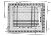
の開口率を向上させることができる。また、共通電極を複数の画素に跨って配置して外周共通電位ラインと接続したので、共通電極への共通電位の供給を低抵抗で十分に行うことができる。
本発明の第1の実施の形態について図面を参照しながら説明する。図1は液晶表示装置の表示領域の一部の平面図であり、図2は図1のX1−X1線に沿った断面図である。実際の液晶表示装置の表示領域70においては、多数の画素がマトリクスに配置されているが、これらの図では3画素のみを示している。
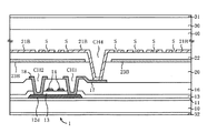
本発明の第2の実施の形態について図面を参照しながら説明する。図9は液晶表示装置の表示領域の一部の平面図であり、図10は図9のX2−X2線に沿った断面図である。また、図11は図9のY1―Y1線に沿った断面図である。実際の液晶表示装置の表示領域においては、多数の画素がマトリクスに配置されているが、これらの図では3画素のみを示している。
本発明の第3の実施の形態について図面を参照しながら説明する。第1、第2の実施の形態においては、画素内のTFT1は能動層がポリシリコンで形成されたポリシリコンTFTであるが、本実施の形態ではその代わりに、能動層がアモルファスシリコンで形成されたアモルファスシリコンTFT1a(以下、aSi−TFT1aという)が用いられている。
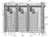
本発明の第4の実施の形態について図面を参照しながら説明する。図15はこの液晶表示装置の表示領域の一部の平面図であり、図16は図15のX4−X4線に沿った断面図である。また、図16は図15のY3―Y3線に沿った断面図である。実際の液晶表示装置の表示領域においては、多数の画素がマトリクスに配置されているが、これらの図では3画素のみを示している。
10,100 TFT基板 11 バッファ層
12 能動層 12d ドレイン領域
12s ソース領域 13,101 ゲート絶縁膜
14,114 ゲートライン 15 共通電極補助ライン
16,104 層間絶縁膜 17,103 ソース電極
18,118 表示信号ライン 19 パッド電極
20 平坦化膜 21,21B,121A,121B 画素電極
22 絶縁膜 23,23A,23B,123A,123B 共通電極
30 対向基板 31,32 偏光板
40 液晶 50 外周共通電位ライン
61 表示信号ライン制御回路 62 ゲートライン制御回路
70 表示領域 102 アモルファスシリコン層
119 接続用配線 150 外周共通電位ライン
CH1〜CH15 コンタクトホール S スリット
Claims (5)
- 基板と、
前記基板上の表示領域に配置された複数の画素と、
前記表示領域の四辺に沿って前記表示領域の外周に配置され、透明電極からなる共通電極に共通電位を供給する外周共通電位ラインと、を備え、
各画素は、画素電極と、この画素電極上に絶縁膜を介して配置され、複数のスリットを有し、複数の画素に跨って配置された前記共通電極とを備え、
前記外周共通電位ラインは、前記表示領域の四辺に沿った外周において、前記共通電極の端部と複数のコンタクトホールを介して接続され、前記外周共通電位ラインの全体は、前記画素に表示信号を供給する表示信号ラインと同じ層であることを特徴とする液晶表示装置。 - 基板と、
前記基板上の表示領域に配置された複数の画素と、
前記表示領域の四辺に沿って前記表示領域の外周に配置され、透明電極からなる共通電極に共通電位を供給する外周共通電位ラインと、を備え、
各画素は、複数の画素に跨って配置された前記共通電極と、この共通電極上に絶縁膜を介して配置され、複数のスリットを有する画素電極とを備え、
前記外周共通電位ラインは、前記表示領域の四辺に沿った外周において、前記共通電極の端部と複数のコンタクトホールを介して接続され、前記外周共通電位ラインの全体は、前記画素に表示信号を供給する表示信号ラインと同じ層であることを特徴とする液晶表示装置。 - 前記外周共通電位ラインは前記表示領域を囲んでおり、前記表示領域と前記外周共通電位ラインとの間のスペースに、前記画素に表示信号を供給する表示信号ラインの制御回路、又は前記画素にゲート信号を供給するゲートラインの制御回路を配置したことを特徴とする請求項1または2に記載の液晶表示装置。
- 前記画素電極に画素選択用の薄膜トランジスタが接続されていることを特徴とする請求項1、2、3いずれかに記載の液晶表示装置。
- 前記共通電極は前記表示領域において一体で形成されていることを特徴とする請求項1、2、3いずれかに記載の液晶表示装置。
Priority Applications (15)
| Application Number | Priority Date | Filing Date | Title |
|---|---|---|---|
| JP2006204624A JP4449953B2 (ja) | 2006-07-27 | 2006-07-27 | 液晶表示装置 |
| TW096124419A TWI369558B (en) | 2006-07-27 | 2007-07-05 | Liquid crystal display device |
| US11/878,579 US20080024416A1 (en) | 2006-07-27 | 2007-07-25 | Liquid crystal display device |
| KR1020070075037A KR100884126B1 (ko) | 2006-07-27 | 2007-07-26 | 액정 표시 장치 |
| CNB2007101392005A CN100510913C (zh) | 2006-07-27 | 2007-07-27 | 液晶显示装置 |
| US13/493,618 US9291863B2 (en) | 2006-07-27 | 2012-06-11 | Liquid crystal display device |
| US15/134,677 US10126608B2 (en) | 2006-07-27 | 2016-04-21 | Liquid crystal display device |
| US15/162,110 US9946125B2 (en) | 2006-07-27 | 2016-05-23 | Liquid crystal display device |
| US15/423,209 US10126609B2 (en) | 2006-07-27 | 2017-02-02 | Liquid crystal display device |
| US16/163,794 US10802353B2 (en) | 2006-07-27 | 2018-10-18 | Liquid crystal display device |
| US16/521,247 US10606133B2 (en) | 2006-07-27 | 2019-07-24 | Liquid crystal display device |
| US16/521,228 US11543708B2 (en) | 2006-07-27 | 2019-07-24 | Display device including common line display device including common line |
| US16/995,368 US11143923B2 (en) | 2006-07-27 | 2020-08-17 | Display device |
| US17/068,039 US11698555B2 (en) | 2006-07-27 | 2020-10-12 | Display device |
| US18/196,725 US20230280619A1 (en) | 2006-07-27 | 2023-05-12 | Display device |
Applications Claiming Priority (1)
| Application Number | Priority Date | Filing Date | Title |
|---|---|---|---|
| JP2006204624A JP4449953B2 (ja) | 2006-07-27 | 2006-07-27 | 液晶表示装置 |
Publications (3)
| Publication Number | Publication Date |
|---|---|
| JP2008032899A JP2008032899A (ja) | 2008-02-14 |
| JP2008032899A5 JP2008032899A5 (ja) | 2008-04-10 |
| JP4449953B2 true JP4449953B2 (ja) | 2010-04-14 |
Family
ID=38985665
Family Applications (1)
| Application Number | Title | Priority Date | Filing Date |
|---|---|---|---|
| JP2006204624A Active JP4449953B2 (ja) | 2006-07-27 | 2006-07-27 | 液晶表示装置 |
Country Status (5)
| Country | Link |
|---|---|
| US (11) | US20080024416A1 (ja) |
| JP (1) | JP4449953B2 (ja) |
| KR (1) | KR100884126B1 (ja) |
| CN (1) | CN100510913C (ja) |
| TW (1) | TWI369558B (ja) |
Families Citing this family (81)
| Publication number | Priority date | Publication date | Assignee | Title |
|---|---|---|---|---|
| JP4449953B2 (ja) * | 2006-07-27 | 2010-04-14 | エプソンイメージングデバイス株式会社 | 液晶表示装置 |
| JP5216204B2 (ja) | 2006-10-31 | 2013-06-19 | 株式会社半導体エネルギー研究所 | 液晶表示装置及びその作製方法 |
| JP5275650B2 (ja) * | 2008-03-12 | 2013-08-28 | 株式会社ジャパンディスプレイウェスト | 液晶表示装置 |
| JP2009223245A (ja) * | 2008-03-19 | 2009-10-01 | Hitachi Displays Ltd | 液晶表示装置 |
| JP5348521B2 (ja) | 2008-06-27 | 2013-11-20 | 株式会社ジャパンディスプレイ | 液晶表示パネル |
| JP5348384B2 (ja) * | 2008-10-01 | 2013-11-20 | 株式会社ジャパンディスプレイ | 液晶表示装置 |
| TWI613489B (zh) | 2008-12-03 | 2018-02-01 | 半導體能源研究所股份有限公司 | 液晶顯示裝置 |
| US20120062451A1 (en) * | 2009-05-13 | 2012-03-15 | Katsuhiko Morishita | Liquid crystal display device |
| JP5389529B2 (ja) * | 2009-05-20 | 2014-01-15 | 株式会社ジャパンディスプレイ | 液晶表示装置及びその製造方法 |
| KR101493662B1 (ko) * | 2009-07-10 | 2015-02-13 | 가부시키가이샤 한도오따이 에네루기 켄큐쇼 | 반도체 장치, 전자 기기 및 표시 패널 |
| US20110085121A1 (en) * | 2009-10-08 | 2011-04-14 | Hydis Technologies Co., Ltd. | Fringe Field Switching Mode Liquid Crystal Display Device and Method of Fabricating the Same |
| KR101790977B1 (ko) * | 2010-10-08 | 2017-10-26 | 엘지디스플레이 주식회사 | 액정표시장치 |
| KR101891985B1 (ko) * | 2010-10-08 | 2018-08-27 | 엘지디스플레이 주식회사 | 액정표시장치 |
| CN102129143A (zh) * | 2010-12-15 | 2011-07-20 | 华映视讯(吴江)有限公司 | 像素阵列基板及其制造方法 |
| KR101924473B1 (ko) * | 2010-12-28 | 2018-12-03 | 엘지디스플레이 주식회사 | 박막 트랜지스터 어레이 기판 및 이의 제조 방법 |
| KR101870986B1 (ko) * | 2011-09-19 | 2018-06-26 | 엘지디스플레이 주식회사 | 박막 트랜지스터 어레이 기판 제조방법 |
| JP5899237B2 (ja) | 2011-11-18 | 2016-04-06 | シャープ株式会社 | 半導体装置、表示装置、ならびに半導体装置の製造方法 |
| US9703150B2 (en) | 2011-11-25 | 2017-07-11 | Sharp Kabushiki Kaisha | Liquid crystal display device |
| WO2013084846A1 (ja) | 2011-12-05 | 2013-06-13 | シャープ株式会社 | 半導体装置 |
| WO2013105537A1 (ja) | 2012-01-11 | 2013-07-18 | シャープ株式会社 | 半導体装置、表示装置、ならびに半導体装置の製造方法 |
| WO2013121956A1 (ja) | 2012-02-15 | 2013-08-22 | シャープ株式会社 | 液晶ディスプレイ |
| JP5912668B2 (ja) * | 2012-03-01 | 2016-04-27 | シャープ株式会社 | 液晶ディスプレイ |
| CN102651342B (zh) | 2012-03-13 | 2014-12-17 | 京东方科技集团股份有限公司 | 阵列基板及其制造方法 |
| CN102790051B (zh) * | 2012-07-27 | 2014-12-10 | 北京京东方光电科技有限公司 | 阵列基板及其制备方法、显示装置 |
| CN102944959B (zh) * | 2012-11-20 | 2014-12-24 | 京东方科技集团股份有限公司 | 阵列基板、其制作方法、其测试方法及显示装置 |
| US9368521B2 (en) | 2012-11-30 | 2016-06-14 | Sharp Kabushiki Kaisha | TFT substrate |
| TWI636309B (zh) * | 2013-07-25 | 2018-09-21 | 日商半導體能源研究所股份有限公司 | 液晶顯示裝置及電子裝置 |
| TWI506501B (zh) * | 2013-08-30 | 2015-11-01 | Ye Xin Technology Consulting Co Ltd | 電子裝置 |
| JP5714679B2 (ja) * | 2013-10-17 | 2015-05-07 | 株式会社ジャパンディスプレイ | 液晶表示装置 |
| CN103529605A (zh) * | 2013-10-29 | 2014-01-22 | 京东方科技集团股份有限公司 | 阵列基板及其制备方法、显示面板及显示装置 |
| WO2015092944A1 (ja) * | 2013-12-19 | 2015-06-25 | パナソニック液晶ディスプレイ株式会社 | 表示装置及び表示装置の製造方法 |
| US9608008B2 (en) | 2014-02-21 | 2017-03-28 | Sharp Kabushiki Kaisha | Active matrix substrate and method for producing same |
| JP6400935B2 (ja) * | 2014-04-17 | 2018-10-03 | 株式会社ジャパンディスプレイ | 表示装置 |
| US9958720B2 (en) | 2014-04-17 | 2018-05-01 | Japan Display Inc. | Display device |
| CN104201178B (zh) * | 2014-08-08 | 2017-04-05 | 京东方科技集团股份有限公司 | 阵列基板及其制备方法、显示装置 |
| CN104216183B (zh) * | 2014-08-28 | 2017-08-29 | 合肥鑫晟光电科技有限公司 | 一种阵列基板及其制备方法、显示装置 |
| CN104280951A (zh) * | 2014-09-23 | 2015-01-14 | 京东方科技集团股份有限公司 | 阵列基板及其制造方法、显示装置 |
| TWI567950B (zh) * | 2015-01-08 | 2017-01-21 | 群創光電股份有限公司 | 顯示面板 |
| CN111665669A (zh) * | 2015-01-08 | 2020-09-15 | 群创光电股份有限公司 | 显示面板 |
| TWI577000B (zh) | 2015-01-21 | 2017-04-01 | 群創光電股份有限公司 | 顯示裝置 |
| KR102381082B1 (ko) * | 2015-07-31 | 2022-03-30 | 엘지디스플레이 주식회사 | 액정 표시 장치 |
| US10388676B2 (en) | 2015-08-10 | 2019-08-20 | Sharp Kabushiki Kaisha | Active matrix substrate and method for producing same, and in-cell touch panel-type display device |
| TWI564644B (zh) * | 2015-08-28 | 2017-01-01 | 群創光電股份有限公司 | 顯示裝置 |
| CN105261621B (zh) * | 2015-09-06 | 2018-01-30 | 京东方科技集团股份有限公司 | 阵列基板及其制作方法、显示装置 |
| CN105204252A (zh) * | 2015-09-23 | 2015-12-30 | 深超光电(深圳)有限公司 | 薄膜晶体管阵列基板及液晶显示面板 |
| CN108352358B (zh) | 2015-10-13 | 2022-07-26 | 非结晶公司 | 非晶金属薄膜非线性电阻器 |
| KR102473647B1 (ko) * | 2015-12-29 | 2022-12-01 | 엘지디스플레이 주식회사 | 액정표시장치 |
| TWI561891B (en) | 2016-01-04 | 2016-12-11 | Au Optronics Corp | Pixel array substrate |
| US10629630B2 (en) | 2016-03-02 | 2020-04-21 | Sharp Kabushiki Kaisha | Active matrix substrate, and liquid crystal display device provided with active matrix substrate |
| WO2017159625A1 (ja) | 2016-03-15 | 2017-09-21 | シャープ株式会社 | アクティブマトリクス基板 |
| US10725336B2 (en) * | 2016-05-20 | 2020-07-28 | Sharp Kabushiki Kaisha | Liquid crystal display panel and liquid crystal display device |
| CN105807523B (zh) | 2016-05-27 | 2020-03-20 | 厦门天马微电子有限公司 | 阵列基板、包含其的显示面板和显示装置 |
| TW201743118A (zh) | 2016-06-08 | 2017-12-16 | 群創光電股份有限公司 | 顯示面板 |
| WO2018030298A1 (ja) | 2016-08-12 | 2018-02-15 | シャープ株式会社 | アクティブマトリクス基板および表示装置 |
| CN109661701A (zh) | 2016-09-01 | 2019-04-19 | 夏普株式会社 | 有源矩阵基板和显示装置 |
| WO2018043643A1 (ja) | 2016-09-02 | 2018-03-08 | シャープ株式会社 | アクティブマトリクス基板およびアクティブマトリクス基板を備えた表示装置 |
| CN109661696B (zh) | 2016-09-05 | 2021-04-13 | 夏普株式会社 | 有源矩阵基板及其制造方法 |
| CN106502012A (zh) * | 2017-01-03 | 2017-03-15 | 深圳市华星光电技术有限公司 | Ffs模式的阵列基板及其制作方法 |
| US10725352B2 (en) | 2017-01-27 | 2020-07-28 | Sharp Kabushiki Kaisha | Active matrix substrate and display device using same |
| CN110291644B (zh) | 2017-02-15 | 2022-11-01 | 夏普株式会社 | 有源矩阵基板 |
| WO2018163997A1 (ja) | 2017-03-09 | 2018-09-13 | シャープ株式会社 | アクティブマトリクス基板およびその製造方法 |
| WO2018212100A1 (ja) | 2017-05-18 | 2018-11-22 | シャープ株式会社 | アクティブマトリクス基板およびその製造方法 |
| CN107422552B (zh) * | 2017-08-16 | 2020-03-27 | 京东方科技集团股份有限公司 | 显示基板以及显示装置 |
| CN107302665B (zh) * | 2017-08-18 | 2020-07-24 | 联想(北京)有限公司 | 一种摄像装置、光圈调节方法和电子设备 |
| JP2019049590A (ja) | 2017-09-08 | 2019-03-28 | シャープ株式会社 | アクティブマトリクス基板およびデマルチプレクサ回路 |
| JP2019050323A (ja) | 2017-09-12 | 2019-03-28 | シャープ株式会社 | アクティブマトリクス基板およびデマルチプレクサ回路 |
| JP7066445B2 (ja) * | 2018-02-20 | 2022-05-13 | 株式会社ジャパンディスプレイ | 表示装置 |
| JP6496433B2 (ja) * | 2018-02-27 | 2019-04-03 | 株式会社半導体エネルギー研究所 | 液晶表示装置 |
| JP6706638B2 (ja) | 2018-03-07 | 2020-06-10 | シャープ株式会社 | 半導体装置およびその製造方法 |
| WO2019191674A2 (en) * | 2018-03-30 | 2019-10-03 | Amorphyx, Incorporated | Amorphous metal thin film transistors |
| CN108983484A (zh) * | 2018-08-06 | 2018-12-11 | 深圳市华星光电技术有限公司 | 一种彩色滤光片及制备方法,显示装置 |
| JP6799123B2 (ja) | 2018-09-19 | 2020-12-09 | シャープ株式会社 | アクティブマトリクス基板およびその製造方法 |
| WO2020065866A1 (ja) * | 2018-09-27 | 2020-04-02 | シャープ株式会社 | 表示装置 |
| CN109521613A (zh) * | 2018-12-24 | 2019-03-26 | 上海天马微电子有限公司 | 一种阵列基板、其制作方法、显示面板及显示装置 |
| CN109742088B (zh) * | 2018-12-29 | 2021-03-16 | 武汉华星光电技术有限公司 | 一种tft阵列基板 |
| US10928691B2 (en) * | 2019-02-15 | 2021-02-23 | Sharp Kabushiki Kaisha | Active matrix substrate comprising a first contact hole that overlaps with a counter electrode control line and passes through a flattening film and liquid crystal display with the same |
| US11695020B2 (en) | 2019-12-17 | 2023-07-04 | Sharp Kabushiki Kaisha | Active matrix substrate and method for manufacturing same |
| US11557679B2 (en) | 2020-03-02 | 2023-01-17 | Sharp Kabushiki Kaisha | Active matrix substrate and display device |
| CN111983862B (zh) * | 2020-08-19 | 2022-07-12 | 武汉华星光电技术有限公司 | 阵列基板、阵列基板制作方法及液晶显示面板 |
| JP2023036194A (ja) * | 2021-09-02 | 2023-03-14 | 株式会社ジャパンディスプレイ | 表示装置 |
| CN115437187B (zh) | 2022-11-09 | 2023-03-24 | 惠科股份有限公司 | 阵列基板和显示面板 |
Family Cites Families (86)
| Publication number | Priority date | Publication date | Assignee | Title |
|---|---|---|---|---|
| TW354380B (en) * | 1995-03-17 | 1999-03-11 | Hitachi Ltd | A liquid crystal device with a wide visual angle |
| US6078318A (en) * | 1995-04-27 | 2000-06-20 | Canon Kabushiki Kaisha | Data transfer method, display driving circuit using the method, and image display apparatus |
| JP3582193B2 (ja) | 1995-12-08 | 2004-10-27 | カシオ計算機株式会社 | 液晶表示素子 |
| JP3170446B2 (ja) | 1996-02-27 | 2001-05-28 | シャープ株式会社 | アクティブマトリクス基板及び液晶表示装置 |
| US5852485A (en) * | 1996-02-27 | 1998-12-22 | Sharp Kabushiki Kaisha | Liquid crystal display device and method for producing the same |
| JPH10133234A (ja) | 1996-09-04 | 1998-05-22 | Toshiba Corp | 液晶表示装置 |
| US20020075422A1 (en) * | 1996-09-19 | 2002-06-20 | Seiko Epson Corporation | Matrix type display device and manufacturing method thereof |
| US6532053B2 (en) | 1996-12-18 | 2003-03-11 | Hitachi, Ltd. | Transverse electric field system liquid crystal display device suitable for improving aperture ratio |
| JPH10186351A (ja) | 1996-12-24 | 1998-07-14 | Hitachi Ltd | 液晶表示装置 |
| JP4024901B2 (ja) | 1997-05-22 | 2007-12-19 | エルジー フィリップス エルシーディー カンパニー リミテッド | アクティブマトリックス型液晶表示装置 |
| KR100251512B1 (ko) * | 1997-07-12 | 2000-04-15 | 구본준 | 횡전계방식 액정표시장치 |
| KR100280874B1 (ko) | 1997-09-12 | 2001-02-01 | 구본준 | 액정패널 |
| JP3831863B2 (ja) * | 1997-10-21 | 2006-10-11 | 大林精工株式会社 | 液晶表示装置 |
| CN1214282C (zh) * | 1997-10-31 | 2005-08-10 | 精工爱普生株式会社 | 电气光学装置及电子设备 |
| US6577368B1 (en) * | 1997-11-03 | 2003-06-10 | Samsung Electronics Co., Ltd. | IPS-LCD having a third electrode having aperture and formed on counter substrate |
| JPH11326928A (ja) * | 1998-05-08 | 1999-11-26 | Hitachi Ltd | 液晶表示装置 |
| JP3766563B2 (ja) | 1999-05-17 | 2006-04-12 | 株式会社日立製作所 | 液晶表示装置 |
| JP3481509B2 (ja) | 1999-06-16 | 2003-12-22 | Nec液晶テクノロジー株式会社 | 液晶表示装置 |
| JP2001083546A (ja) * | 1999-07-12 | 2001-03-30 | Hitachi Ltd | 液晶表示装置 |
| TW457384B (en) * | 1999-09-13 | 2001-10-01 | Ind Tech Res Inst | Electrode structure for a wide viewing angle liquid crystal display |
| US6927824B1 (en) * | 1999-09-16 | 2005-08-09 | Fujitsu Display Technologies Corporation | Liquid crystal display device and thin film transistor substrate |
| CN1195243C (zh) * | 1999-09-30 | 2005-03-30 | 三星电子株式会社 | 用于液晶显示器的薄膜晶体管阵列屏板及其制造方法 |
| JP2001102169A (ja) * | 1999-10-01 | 2001-04-13 | Sanyo Electric Co Ltd | El表示装置 |
| JP3379491B2 (ja) * | 1999-10-22 | 2003-02-24 | 日本電気株式会社 | 液晶表示装置 |
| JP3687452B2 (ja) | 1999-12-27 | 2005-08-24 | 株式会社日立製作所 | 液晶表示装置 |
| JP3832261B2 (ja) | 2000-03-16 | 2006-10-11 | セイコーエプソン株式会社 | 液晶装置、投射型表示装置及び電子機器 |
| JP2001272697A (ja) | 2000-03-23 | 2001-10-05 | Hitachi Ltd | 液晶表示装置 |
| US6500701B2 (en) * | 2000-04-28 | 2002-12-31 | Casio Computer Co., Ltd. | Method of manufacturing thin film transistor panel having protective film of channel region |
| KR100633315B1 (ko) * | 2000-06-01 | 2006-10-11 | 엘지.필립스 엘시디 주식회사 | 축적용량방식용 액정표시장치의 공통전극 배선과,횡전계모드용 액정표시장치의 스토리지전극 배선의 구조 |
| JP2001354968A (ja) | 2000-06-09 | 2001-12-25 | Hitachi Ltd | アクティブ・マトリクス型液晶表示装置およびその液晶組成物質 |
| JP4446577B2 (ja) * | 2000-09-06 | 2010-04-07 | エーユー オプトロニクス コーポレイション | 表示パネル、表示装置 |
| KR100601454B1 (ko) | 2000-10-04 | 2006-07-14 | 엘지.필립스 엘시디 주식회사 | 멀티 도메인 액정표시장치 및 그 제조방법 |
| US6784966B2 (en) * | 2001-03-06 | 2004-08-31 | Seiko Epson Corp. | Liquid crystal device, projection type display and electronic equipment |
| JP4556341B2 (ja) | 2001-03-30 | 2010-10-06 | セイコーエプソン株式会社 | 液晶表示装置および電子機器 |
| JP3618302B2 (ja) | 2001-04-10 | 2005-02-09 | 松下電器産業株式会社 | 液晶パネルの検査法及び検査装置 |
| JP4041336B2 (ja) * | 2001-06-29 | 2008-01-30 | シャープ株式会社 | 液晶表示装置用基板及びそれを備えた液晶表示装置及びその製造方法 |
| JP4353660B2 (ja) | 2001-07-27 | 2009-10-28 | 三洋電機株式会社 | アクティブマトリクス型表示装置 |
| JP2003090994A (ja) | 2001-09-19 | 2003-03-28 | Hitachi Ltd | 液晶表示装置 |
| JP3909572B2 (ja) * | 2001-09-28 | 2007-04-25 | 株式会社日立製作所 | 表示装置 |
| US6778229B2 (en) * | 2001-10-02 | 2004-08-17 | Fujitsu Display Technologies Corporation | Liquid crystal display device and method of fabricating the same |
| JP4305811B2 (ja) * | 2001-10-15 | 2009-07-29 | 株式会社日立製作所 | 液晶表示装置、画像表示装置およびその製造方法 |
| JP2003131248A (ja) | 2001-10-25 | 2003-05-08 | Seiko Epson Corp | 液晶表示装置および液晶表示装置の製造方法並びに液晶表示装置用基板、電子機器 |
| KR100652046B1 (ko) * | 2001-12-22 | 2006-11-30 | 엘지.필립스 엘시디 주식회사 | 액정표시소자 및 그 제조방법 |
| KR100450701B1 (ko) * | 2001-12-28 | 2004-10-01 | 엘지.필립스 엘시디 주식회사 | 액정표시장치용 어레이기판과 그 제조방법 |
| JP3920649B2 (ja) | 2002-01-31 | 2007-05-30 | 株式会社日立製作所 | 画像表示装置および液晶表示装置 |
| US7102726B2 (en) * | 2002-03-15 | 2006-09-05 | Lg. Philips Lcd Co., Ltd. | System for fabricating liquid crystal display and method of fabricating liquid crystal display using the same |
| JP2003295207A (ja) | 2002-03-29 | 2003-10-15 | Nec Lcd Technologies Ltd | 横電界方式のアクティブマトリクス型液晶表示装置 |
| JP4005410B2 (ja) | 2002-05-15 | 2007-11-07 | 株式会社 日立ディスプレイズ | 画像表示装置 |
| JP3778176B2 (ja) * | 2002-05-28 | 2006-05-24 | セイコーエプソン株式会社 | 発光装置および電子機器 |
| JP4085170B2 (ja) * | 2002-06-06 | 2008-05-14 | 株式会社 日立ディスプレイズ | 液晶表示装置 |
| JP3700714B2 (ja) * | 2002-06-21 | 2005-09-28 | セイコーエプソン株式会社 | 電気光学装置及び電子機器 |
| JP4145637B2 (ja) | 2002-11-25 | 2008-09-03 | シャープ株式会社 | アクティブマトリクス基板及び表示装置 |
| US6762815B2 (en) * | 2002-12-12 | 2004-07-13 | Hannstar Display Corp. | In-plane switching LCD with a redundancy structure for an opened common electrode and a high storage capacitance |
| KR100911470B1 (ko) | 2003-01-30 | 2009-08-11 | 삼성전자주식회사 | 액정표시장치 |
| KR100741890B1 (ko) * | 2003-06-26 | 2007-07-23 | 엘지.필립스 엘시디 주식회사 | 횡전계 방식의 액정표시장치 및 그의 제조방법 |
| KR101085150B1 (ko) | 2003-06-28 | 2011-11-18 | 엘지디스플레이 주식회사 | 횡전계 방식의 액정표시장치 및 그의 제조방법 |
| TW594177B (en) | 2003-07-23 | 2004-06-21 | Hannstar Display Corp | Liquid crystal display panel for eliminating flicker |
| JP2005070541A (ja) | 2003-08-26 | 2005-03-17 | Seiko Epson Corp | 液晶表示装置及び携帯型電子機器 |
| KR101007206B1 (ko) | 2003-12-11 | 2011-01-12 | 엘지디스플레이 주식회사 | 프린지 필드 스위칭 모드 액정표시장치 및 그 제조방법 |
| CN1627146A (zh) * | 2003-12-13 | 2005-06-15 | 鸿富锦精密工业(深圳)有限公司 | 边缘电场开关型液晶显示装置 |
| KR100640212B1 (ko) * | 2003-12-16 | 2006-10-31 | 엘지.필립스 엘시디 주식회사 | 공통전극의 접속이 강화된 횡전계방식 액정표시패널 및 그 제조방법 |
| KR20050067735A (ko) * | 2003-12-29 | 2005-07-05 | 비오이 하이디스 테크놀로지 주식회사 | 프린지 필드 스위칭 모드 액정표시장치 |
| US7372513B2 (en) * | 2003-12-30 | 2008-05-13 | Lg.Philips Lcd Co., Ltd. | Liquid crystal display device and method for fabricating the same |
| KR100710164B1 (ko) * | 2003-12-30 | 2007-04-20 | 엘지.필립스 엘시디 주식회사 | 횡전계 방식 액정 표시 장치 |
| JP4011557B2 (ja) | 2004-03-25 | 2007-11-21 | 三菱電機株式会社 | 液晶表示装置および液晶表示装置の製造方法 |
| JP4462981B2 (ja) * | 2004-03-29 | 2010-05-12 | Nec液晶テクノロジー株式会社 | アクティブマトリクス基板及び該基板を備える液晶表示装置 |
| JP4627148B2 (ja) * | 2004-04-09 | 2011-02-09 | 株式会社 日立ディスプレイズ | 表示装置 |
| JP4230425B2 (ja) | 2004-07-26 | 2009-02-25 | シャープ株式会社 | カラーフィルタ基板、および表示装置 |
| KR100590932B1 (ko) * | 2004-09-23 | 2006-06-19 | 비오이 하이디스 테크놀로지 주식회사 | 프린지 필드 스위칭 모드 액정표시장치 |
| KR100583138B1 (ko) * | 2004-10-08 | 2006-05-23 | 삼성에스디아이 주식회사 | 발광 표시장치 |
| KR101085136B1 (ko) * | 2004-12-04 | 2011-11-18 | 엘지디스플레이 주식회사 | 수평 전계 박막 트랜지스터 기판 및 그 제조 방법 |
| KR101107239B1 (ko) * | 2004-12-23 | 2012-01-25 | 엘지디스플레이 주식회사 | 액정 표시 패널 및 그 제조방법 |
| KR100719922B1 (ko) * | 2005-03-03 | 2007-05-18 | 비오이 하이디스 테크놀로지 주식회사 | 프린지 필드 스위칭 모드 액정표시장치 |
| US7710739B2 (en) * | 2005-04-28 | 2010-05-04 | Semiconductor Energy Laboratory Co., Ltd. | Semiconductor device and display device |
| KR101159318B1 (ko) * | 2005-05-31 | 2012-06-22 | 엘지디스플레이 주식회사 | 액정 표시 장치 |
| JP4400588B2 (ja) | 2005-06-02 | 2010-01-20 | エプソンイメージングデバイス株式会社 | 電気光学装置、電気光学装置の駆動方法、および、電子機器 |
| KR20070010618A (ko) | 2005-07-19 | 2007-01-24 | 삼성전자주식회사 | 표시 장치 및 박막 트랜지스터 표시판 |
| JP4827499B2 (ja) | 2005-11-16 | 2011-11-30 | キヤノン株式会社 | 電流駆動型装置及び表示装置 |
| KR101201068B1 (ko) * | 2005-12-20 | 2012-11-14 | 엘지디스플레이 주식회사 | 액정 표시 장치 및 그 제조방법 |
| KR101177593B1 (ko) * | 2005-12-29 | 2012-08-27 | 엘지디스플레이 주식회사 | 액정표시장치 |
| ATE486298T1 (de) * | 2006-05-19 | 2010-11-15 | Sharp Kk | Anzeigevorrichtung |
| JP4884846B2 (ja) * | 2006-05-31 | 2012-02-29 | 株式会社 日立ディスプレイズ | 液晶表示装置 |
| JP4449953B2 (ja) * | 2006-07-27 | 2010-04-14 | エプソンイメージングデバイス株式会社 | 液晶表示装置 |
| JP5191639B2 (ja) * | 2006-09-15 | 2013-05-08 | 株式会社ジャパンディスプレイイースト | 液晶表示装置 |
| US8681305B2 (en) * | 2008-12-24 | 2014-03-25 | Lg Display Co., Ltd. | Liquid crystal display device comprising a common line pattern formed correspond to the conductive seal pattern, a transparent electrode pattern overlapping the common line pattern with an insulating layer interposed there between, the transparent electrode pattern having a width equal to or less than that of the common line pattern |
| JP5013554B2 (ja) | 2010-03-31 | 2012-08-29 | 株式会社ジャパンディスプレイセントラル | 液晶表示装置 |
-
2006
- 2006-07-27 JP JP2006204624A patent/JP4449953B2/ja active Active
-
2007
- 2007-07-05 TW TW096124419A patent/TWI369558B/zh active
- 2007-07-25 US US11/878,579 patent/US20080024416A1/en not_active Abandoned
- 2007-07-26 KR KR1020070075037A patent/KR100884126B1/ko active IP Right Grant
- 2007-07-27 CN CNB2007101392005A patent/CN100510913C/zh active Active
-
2012
- 2012-06-11 US US13/493,618 patent/US9291863B2/en active Active
-
2016
- 2016-04-21 US US15/134,677 patent/US10126608B2/en active Active
- 2016-05-23 US US15/162,110 patent/US9946125B2/en active Active
-
2017
- 2017-02-02 US US15/423,209 patent/US10126609B2/en active Active
-
2018
- 2018-10-18 US US16/163,794 patent/US10802353B2/en active Active
-
2019
- 2019-07-24 US US16/521,228 patent/US11543708B2/en active Active
- 2019-07-24 US US16/521,247 patent/US10606133B2/en active Active
-
2020
- 2020-08-17 US US16/995,368 patent/US11143923B2/en active Active
- 2020-10-12 US US17/068,039 patent/US11698555B2/en active Active
-
2023
- 2023-05-12 US US18/196,725 patent/US20230280619A1/en active Pending
Also Published As
| Publication number | Publication date |
|---|---|
| US11698555B2 (en) | 2023-07-11 |
| US20080024416A1 (en) | 2008-01-31 |
| US20120313845A1 (en) | 2012-12-13 |
| US20160266453A1 (en) | 2016-09-15 |
| US10126609B2 (en) | 2018-11-13 |
| US20210026207A1 (en) | 2021-01-28 |
| US20190346724A1 (en) | 2019-11-14 |
| US20190049800A1 (en) | 2019-02-14 |
| US11543708B2 (en) | 2023-01-03 |
| CN100510913C (zh) | 2009-07-08 |
| TWI369558B (en) | 2012-08-01 |
| US20230280619A1 (en) | 2023-09-07 |
| TW200807122A (en) | 2008-02-01 |
| US20160231628A1 (en) | 2016-08-11 |
| KR20080011085A (ko) | 2008-01-31 |
| KR100884126B1 (ko) | 2009-02-17 |
| US9946125B2 (en) | 2018-04-17 |
| US20170146873A1 (en) | 2017-05-25 |
| CN101114086A (zh) | 2008-01-30 |
| US20200379305A1 (en) | 2020-12-03 |
| JP2008032899A (ja) | 2008-02-14 |
| US11143923B2 (en) | 2021-10-12 |
| US10802353B2 (en) | 2020-10-13 |
| US10126608B2 (en) | 2018-11-13 |
| US20190346725A1 (en) | 2019-11-14 |
| US10606133B2 (en) | 2020-03-31 |
| US9291863B2 (en) | 2016-03-22 |
Similar Documents
| Publication | Publication Date | Title |
|---|---|---|
| JP4449953B2 (ja) | 液晶表示装置 | |
| JP4797740B2 (ja) | 液晶表示装置 | |
| JP5079448B2 (ja) | 液晶装置及びそれを備えた電子機器 | |
| JP5392670B2 (ja) | 液晶表示装置及びその製造方法 | |
| JP2007226175A (ja) | 液晶装置及び電子機器 | |
| JP2018063348A (ja) | 液晶表示パネルおよび液晶表示装置 | |
| JP2007293155A (ja) | 液晶表示装置 | |
| JP2006189830A (ja) | 液晶表示装置およびその製造方法 | |
| JP5106991B2 (ja) | 液晶装置および電子機器 | |
| JP5683874B2 (ja) | 薄膜トランジスタアレイパネル及びその製造方法 | |
| JP2007226200A (ja) | 液晶装置及び電子機器 | |
| US10168581B2 (en) | Display device | |
| US20060285046A1 (en) | Liquid crystal display device and method of fabricating the same | |
| US9864237B2 (en) | Display device | |
| JP5072530B2 (ja) | 液晶装置及びそれを備えた電子機器 | |
| JP2023064656A (ja) | アクティブマトリクス基板、表示パネル、及び表示装置 | |
| KR20090003608A (ko) | 박막트랜지스터 기판 및 그의 형성방법과 리페어 방법 | |
| JP2008020491A (ja) | 液晶表示装置 | |
| JP2006058329A (ja) | 電気光学装置及び電子機器 |
Legal Events
| Date | Code | Title | Description |
|---|---|---|---|
| A521 | Request for written amendment filed |
Free format text: JAPANESE INTERMEDIATE CODE: A523 Effective date: 20080225 |
|
| A621 | Written request for application examination |
Free format text: JAPANESE INTERMEDIATE CODE: A621 Effective date: 20080225 |
|
| A131 | Notification of reasons for refusal |
Free format text: JAPANESE INTERMEDIATE CODE: A131 Effective date: 20080513 |
|
| A977 | Report on retrieval |
Free format text: JAPANESE INTERMEDIATE CODE: A971007 Effective date: 20080513 |
|
| A521 | Request for written amendment filed |
Free format text: JAPANESE INTERMEDIATE CODE: A523 Effective date: 20080711 |
|
| A131 | Notification of reasons for refusal |
Free format text: JAPANESE INTERMEDIATE CODE: A131 Effective date: 20090120 |
|
| A521 | Request for written amendment filed |
Free format text: JAPANESE INTERMEDIATE CODE: A523 Effective date: 20090319 |
|
| A02 | Decision of refusal |
Free format text: JAPANESE INTERMEDIATE CODE: A02 Effective date: 20090817 |
|
| A521 | Request for written amendment filed |
Free format text: JAPANESE INTERMEDIATE CODE: A523 Effective date: 20091110 |
|
| A911 | Transfer to examiner for re-examination before appeal (zenchi) |
Free format text: JAPANESE INTERMEDIATE CODE: A911 Effective date: 20091124 |
|
| TRDD | Decision of grant or rejection written | ||
| A01 | Written decision to grant a patent or to grant a registration (utility model) |
Free format text: JAPANESE INTERMEDIATE CODE: A01 Effective date: 20100105 |
|
| A01 | Written decision to grant a patent or to grant a registration (utility model) |
Free format text: JAPANESE INTERMEDIATE CODE: A01 |
|
| A61 | First payment of annual fees (during grant procedure) |
Free format text: JAPANESE INTERMEDIATE CODE: A61 Effective date: 20100118 |
|
| R150 | Certificate of patent or registration of utility model |
Ref document number: 4449953 Country of ref document: JP Free format text: JAPANESE INTERMEDIATE CODE: R150 Free format text: JAPANESE INTERMEDIATE CODE: R150 |
|
| FPAY | Renewal fee payment (event date is renewal date of database) |
Free format text: PAYMENT UNTIL: 20130205 Year of fee payment: 3 |
|
| FPAY | Renewal fee payment (event date is renewal date of database) |
Free format text: PAYMENT UNTIL: 20130205 Year of fee payment: 3 |
|
| S111 | Request for change of ownership or part of ownership |
Free format text: JAPANESE INTERMEDIATE CODE: R313113 |
|
| FPAY | Renewal fee payment (event date is renewal date of database) |
Free format text: PAYMENT UNTIL: 20130205 Year of fee payment: 3 |
|
| R360 | Written notification for declining of transfer of rights |
Free format text: JAPANESE INTERMEDIATE CODE: R360 |
|
| FPAY | Renewal fee payment (event date is renewal date of database) |
Free format text: PAYMENT UNTIL: 20130205 Year of fee payment: 3 |
|
| S111 | Request for change of ownership or part of ownership |
Free format text: JAPANESE INTERMEDIATE CODE: R313113 |
|
| FPAY | Renewal fee payment (event date is renewal date of database) |
Free format text: PAYMENT UNTIL: 20130205 Year of fee payment: 3 |
|
| R350 | Written notification of registration of transfer |
Free format text: JAPANESE INTERMEDIATE CODE: R350 |
|
| FPAY | Renewal fee payment (event date is renewal date of database) |
Free format text: PAYMENT UNTIL: 20130205 Year of fee payment: 3 |
|
| FPAY | Renewal fee payment (event date is renewal date of database) |
Free format text: PAYMENT UNTIL: 20130205 Year of fee payment: 3 |
|
| S111 | Request for change of ownership or part of ownership |
Free format text: JAPANESE INTERMEDIATE CODE: R313113 |
|
| FPAY | Renewal fee payment (event date is renewal date of database) |
Free format text: PAYMENT UNTIL: 20130205 Year of fee payment: 3 |
|
| R350 | Written notification of registration of transfer |
Free format text: JAPANESE INTERMEDIATE CODE: R350 |
|
| FPAY | Renewal fee payment (event date is renewal date of database) |
Free format text: PAYMENT UNTIL: 20130205 Year of fee payment: 3 |
|
| FPAY | Renewal fee payment (event date is renewal date of database) |
Free format text: PAYMENT UNTIL: 20140205 Year of fee payment: 4 |
|
| R250 | Receipt of annual fees |
Free format text: JAPANESE INTERMEDIATE CODE: R250 |
|
| R250 | Receipt of annual fees |
Free format text: JAPANESE INTERMEDIATE CODE: R250 |
|
| R250 | Receipt of annual fees |
Free format text: JAPANESE INTERMEDIATE CODE: R250 |
|
| R250 | Receipt of annual fees |
Free format text: JAPANESE INTERMEDIATE CODE: R250 |
|
| R250 | Receipt of annual fees |
Free format text: JAPANESE INTERMEDIATE CODE: R250 |
|
| R250 | Receipt of annual fees |
Free format text: JAPANESE INTERMEDIATE CODE: R250 |
|
| R250 | Receipt of annual fees |
Free format text: JAPANESE INTERMEDIATE CODE: R250 |
|
| R250 | Receipt of annual fees |
Free format text: JAPANESE INTERMEDIATE CODE: R250 |
|
| R250 | Receipt of annual fees |
Free format text: JAPANESE INTERMEDIATE CODE: R250 |
|
| S111 | Request for change of ownership or part of ownership |
Free format text: JAPANESE INTERMEDIATE CODE: R313111 |
|
| R350 | Written notification of registration of transfer |
Free format text: JAPANESE INTERMEDIATE CODE: R350 |
|
| R250 | Receipt of annual fees |
Free format text: JAPANESE INTERMEDIATE CODE: R250 |
|
| R250 | Receipt of annual fees |
Free format text: JAPANESE INTERMEDIATE CODE: R250 |
|
| R250 | Receipt of annual fees |
Free format text: JAPANESE INTERMEDIATE CODE: R250 |