JP5191639B2 - 液晶表示装置 - Google Patents
液晶表示装置 Download PDFInfo
- Publication number
- JP5191639B2 JP5191639B2 JP2006250989A JP2006250989A JP5191639B2 JP 5191639 B2 JP5191639 B2 JP 5191639B2 JP 2006250989 A JP2006250989 A JP 2006250989A JP 2006250989 A JP2006250989 A JP 2006250989A JP 5191639 B2 JP5191639 B2 JP 5191639B2
- Authority
- JP
- Japan
- Prior art keywords
- potential
- scanning signal
- signal line
- video signal
- electrode
- Prior art date
- Legal status (The legal status is an assumption and is not a legal conclusion. Google has not performed a legal analysis and makes no representation as to the accuracy of the status listed.)
- Active
Links
- 239000004973 liquid crystal related substance Substances 0.000 title claims description 123
- 239000000758 substrate Substances 0.000 claims description 68
- 230000005684 electric field Effects 0.000 claims description 25
- 239000003990 capacitor Substances 0.000 claims description 20
- 239000000463 material Substances 0.000 claims description 11
- 239000010409 thin film Substances 0.000 claims description 3
- 239000010408 film Substances 0.000 description 39
- 238000000034 method Methods 0.000 description 25
- 238000010586 diagram Methods 0.000 description 16
- 238000005530 etching Methods 0.000 description 14
- 101100060179 Drosophila melanogaster Clk gene Proteins 0.000 description 8
- 101150038023 PEX1 gene Proteins 0.000 description 8
- 239000011159 matrix material Substances 0.000 description 8
- 101150014555 pas-1 gene Proteins 0.000 description 8
- 101100016388 Arabidopsis thaliana PAS2 gene Proteins 0.000 description 7
- 101100297150 Komagataella pastoris PEX3 gene Proteins 0.000 description 7
- 101100315760 Saccharomyces cerevisiae (strain ATCC 204508 / S288c) PEX4 gene Proteins 0.000 description 7
- 238000002834 transmittance Methods 0.000 description 6
- 102100036464 Activated RNA polymerase II transcriptional coactivator p15 Human genes 0.000 description 5
- 101000713904 Homo sapiens Activated RNA polymerase II transcriptional coactivator p15 Proteins 0.000 description 5
- 229910004444 SUB1 Inorganic materials 0.000 description 5
- 239000004020 conductor Substances 0.000 description 5
- 239000011521 glass Substances 0.000 description 5
- 229910004438 SUB2 Inorganic materials 0.000 description 4
- 101100311330 Schizosaccharomyces pombe (strain 972 / ATCC 24843) uap56 gene Proteins 0.000 description 4
- OSDXSOSJRPQCHJ-XVNBXDOJSA-N methyl 3-(3,4-dihydroxyphenyl)-3-[(E)-3-(3,4-dihydroxyphenyl)prop-2-enoyl]oxypropanoate Chemical compound C=1C=C(O)C(O)=CC=1C(CC(=O)OC)OC(=O)\C=C\C1=CC=C(O)C(O)=C1 OSDXSOSJRPQCHJ-XVNBXDOJSA-N 0.000 description 4
- 239000004065 semiconductor Substances 0.000 description 4
- 101150018444 sub2 gene Proteins 0.000 description 4
- XAGFODPZIPBFFR-UHFFFAOYSA-N aluminium Chemical compound [Al] XAGFODPZIPBFFR-UHFFFAOYSA-N 0.000 description 3
- 229910052782 aluminium Inorganic materials 0.000 description 3
- 229910021417 amorphous silicon Inorganic materials 0.000 description 2
- 230000006866 deterioration Effects 0.000 description 2
- 230000014759 maintenance of location Effects 0.000 description 2
- 230000009193 crawling Effects 0.000 description 1
- 230000006870 function Effects 0.000 description 1
- 230000020169 heat generation Effects 0.000 description 1
- 239000012535 impurity Substances 0.000 description 1
- 238000012986 modification Methods 0.000 description 1
- 230000004048 modification Effects 0.000 description 1
- 238000007789 sealing Methods 0.000 description 1
- 230000001360 synchronised effect Effects 0.000 description 1
Images


Classifications
-
- G—PHYSICS
- G09—EDUCATION; CRYPTOGRAPHY; DISPLAY; ADVERTISING; SEALS
- G09G—ARRANGEMENTS OR CIRCUITS FOR CONTROL OF INDICATING DEVICES USING STATIC MEANS TO PRESENT VARIABLE INFORMATION
- G09G3/00—Control arrangements or circuits, of interest only in connection with visual indicators other than cathode-ray tubes
- G09G3/20—Control arrangements or circuits, of interest only in connection with visual indicators other than cathode-ray tubes for presentation of an assembly of a number of characters, e.g. a page, by composing the assembly by combination of individual elements arranged in a matrix no fixed position being assigned to or needed to be assigned to the individual characters or partial characters
- G09G3/34—Control arrangements or circuits, of interest only in connection with visual indicators other than cathode-ray tubes for presentation of an assembly of a number of characters, e.g. a page, by composing the assembly by combination of individual elements arranged in a matrix no fixed position being assigned to or needed to be assigned to the individual characters or partial characters by control of light from an independent source
- G09G3/36—Control arrangements or circuits, of interest only in connection with visual indicators other than cathode-ray tubes for presentation of an assembly of a number of characters, e.g. a page, by composing the assembly by combination of individual elements arranged in a matrix no fixed position being assigned to or needed to be assigned to the individual characters or partial characters by control of light from an independent source using liquid crystals
- G09G3/3611—Control of matrices with row and column drivers
- G09G3/3648—Control of matrices with row and column drivers using an active matrix
-
- G—PHYSICS
- G09—EDUCATION; CRYPTOGRAPHY; DISPLAY; ADVERTISING; SEALS
- G09G—ARRANGEMENTS OR CIRCUITS FOR CONTROL OF INDICATING DEVICES USING STATIC MEANS TO PRESENT VARIABLE INFORMATION
- G09G2300/00—Aspects of the constitution of display devices
- G09G2300/04—Structural and physical details of display devices
- G09G2300/0421—Structural details of the set of electrodes
- G09G2300/0426—Layout of electrodes and connections
-
- G—PHYSICS
- G09—EDUCATION; CRYPTOGRAPHY; DISPLAY; ADVERTISING; SEALS
- G09G—ARRANGEMENTS OR CIRCUITS FOR CONTROL OF INDICATING DEVICES USING STATIC MEANS TO PRESENT VARIABLE INFORMATION
- G09G3/00—Control arrangements or circuits, of interest only in connection with visual indicators other than cathode-ray tubes
- G09G3/20—Control arrangements or circuits, of interest only in connection with visual indicators other than cathode-ray tubes for presentation of an assembly of a number of characters, e.g. a page, by composing the assembly by combination of individual elements arranged in a matrix no fixed position being assigned to or needed to be assigned to the individual characters or partial characters
- G09G3/34—Control arrangements or circuits, of interest only in connection with visual indicators other than cathode-ray tubes for presentation of an assembly of a number of characters, e.g. a page, by composing the assembly by combination of individual elements arranged in a matrix no fixed position being assigned to or needed to be assigned to the individual characters or partial characters by control of light from an independent source
- G09G3/36—Control arrangements or circuits, of interest only in connection with visual indicators other than cathode-ray tubes for presentation of an assembly of a number of characters, e.g. a page, by composing the assembly by combination of individual elements arranged in a matrix no fixed position being assigned to or needed to be assigned to the individual characters or partial characters by control of light from an independent source using liquid crystals
- G09G3/3607—Control arrangements or circuits, of interest only in connection with visual indicators other than cathode-ray tubes for presentation of an assembly of a number of characters, e.g. a page, by composing the assembly by combination of individual elements arranged in a matrix no fixed position being assigned to or needed to be assigned to the individual characters or partial characters by control of light from an independent source using liquid crystals for displaying colours or for displaying grey scales with a specific pixel layout, e.g. using sub-pixels
-
- G—PHYSICS
- G09—EDUCATION; CRYPTOGRAPHY; DISPLAY; ADVERTISING; SEALS
- G09G—ARRANGEMENTS OR CIRCUITS FOR CONTROL OF INDICATING DEVICES USING STATIC MEANS TO PRESENT VARIABLE INFORMATION
- G09G3/00—Control arrangements or circuits, of interest only in connection with visual indicators other than cathode-ray tubes
- G09G3/20—Control arrangements or circuits, of interest only in connection with visual indicators other than cathode-ray tubes for presentation of an assembly of a number of characters, e.g. a page, by composing the assembly by combination of individual elements arranged in a matrix no fixed position being assigned to or needed to be assigned to the individual characters or partial characters
- G09G3/34—Control arrangements or circuits, of interest only in connection with visual indicators other than cathode-ray tubes for presentation of an assembly of a number of characters, e.g. a page, by composing the assembly by combination of individual elements arranged in a matrix no fixed position being assigned to or needed to be assigned to the individual characters or partial characters by control of light from an independent source
- G09G3/36—Control arrangements or circuits, of interest only in connection with visual indicators other than cathode-ray tubes for presentation of an assembly of a number of characters, e.g. a page, by composing the assembly by combination of individual elements arranged in a matrix no fixed position being assigned to or needed to be assigned to the individual characters or partial characters by control of light from an independent source using liquid crystals
- G09G3/3611—Control of matrices with row and column drivers
- G09G3/3614—Control of polarity reversal in general
Description
(2)前記(1)の液晶表示装置において、前記スイッチング素子は、TFT(Thin Film Transistor)であり、前記TFTのゲート電極は前記走査信号線に接続され、前記TFTのドレイン電極またはソース電極のいずれか一方は前記映像信号線に接続され、前記TFTのドレイン電極またはソース電極のうちの前記映像信号線に接続されていないほうは前記画素電極に接続されている液晶表示装置。
(3)前記(1)の液晶表示装置において、前記表示パネルは、一対の基板を有し、前記画素電極と前記共通電極とは、同じ前記基板の上に形成されており、当該表示パネルは、横電界方式で動作する液晶表示装置。
(4)前記(1)の液晶表示装置において、前記表示パネルは、一対の基板を有し、前記画素電極と前記共通電極とは、異なる前記基板の上に形成されており、当該表示パネルは、縦電界方式で動作する液晶表示装置。
(6)前記(5)の液晶表示装置において、前記スイッチング素子は、TFTであり、前記TFTのゲート電極は前記走査信号線に接続され、前記TFTのドレイン電極またはソース電極のいずれか一方は前記映像信号線に接続され、前記TFTのドレイン電極またはソース電極のうちの前記映像信号線に接続されていないほうは前記画素電極に接続されている液晶表示装置。
(7)前記(5)の液晶表示装置において、前記画素電極と前記共通電極とは、同じ基板の上に形成されており、前記表示パネルは、横電界方式で動作する液晶表示装置。
(8)前記(5)の液晶表示装置において、前記画素電極と前記共通電極とは、異なる基板の上に形成されており、前記表示パネルは、縦電界方式で動作する液晶表示装置。
なお、実施例を説明するための全図において、同一機能を有するものは、同一符号を付け、その繰り返しの説明は省略する。
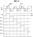
図2(a)は、本実施例の液晶表示パネルの一構成例と1フレーム期間における画素電極の極性を示す模式回路図である。図2(b)は、図2(a)に示した構成の液晶表示パネルにおける駆動方法の一例を示す模式図である。
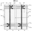
図4(a)は、図3(a)および図3(b)に示した液晶表示パネルにおけるTFT基板の第1の構成例を示す模式平面図である。図4(b)は、図4(a)のB−B’線における液晶表示パネルの断面構成の一例を示す模式断面図である。
101…TFT基板
102…対向基板
103,LC…液晶材料
104…シール材
105A,105B…偏光板
SUB1,SUB2…絶縁基板
DL,DL1,DL2,DL3,DL4,DL5…映像信号線
GL,GL1,GL2,GLn−1,GLn,GLn+1,GLn+2,GLn+3,GLn+4,GLn+5,GLn+6…走査信号線
PX…画素電極
CT…対向電極
StgL…保持容量線
SD1…ドレイン電極
SD2…ソース電極
PAS1,PAS2…絶縁層
ORI1,ORI2…配向膜
BM…遮光膜
CF…カラーフィルタ
OC…オーバーコート層
2…データドライバ
3…走査ドライバ
4…共通電圧制御回路
Claims (8)
- 複数本の映像信号線と、複数本の走査信号線と、スイッチング素子および画素電極を有し前記画素電極および液晶材料ならびに共通電極により画素容量を形成する画素とを有し、前記映像信号線の延在方向および前記走査信号線の延在方向のそれぞれに複数個ずつ前記画素を並べて構成される表示領域を有する表示パネルと、
前記複数本の映像信号線に映像信号を入力する第1の駆動回路と、
前記複数本の走査信号線に順番に走査信号を入力する第2の駆動回路と、
前記共通電極に入力する共通電圧の電位を制御する共通電圧制御回路とを有する液晶表示装置であって、
前記複数本の映像信号線は、前記走査信号線の延在方向に一列に並んだ複数の画素電極に対して、2つの隣接する画素電極毎に1本ずつ配置されており、
前記複数本の走査信号線は、前記映像信号線の延在方向に並んで隣接する2つの画素電極の間に2本ずつ配置され、かつ、前記走査信号線の延在方向に一列に並んだ複数の画素電極に対して該複数の画素電極を挟むように2本ずつ配置されており、
前記走査信号線の延在方向に一列に並んだ複数の画素は、前記複数の画素の画素電極を挟むように配置された2本の走査信号線のうちの第1の走査信号線にスイッチング素子が接続された画素と、前記2本の走査信号線のうちの第2の走査信号線にスイッチング素子が接続された画素とが、交互に配置されており、
1本の前記映像信号線を挟んで隣接する2つの画素は、各画素のスイッチング素子が前記1本の前記映像信号線に接続されており、かつ、前記2本の走査信号線のうちの前記第1の走査信号線にスイッチング素子が接続された画素と、前記2本の走査信号線のうちの第2の走査信号線にスイッチング素子が接続された画素との位置が、前記映像信号線の延在方向に並んだ前記2つの画素の組毎に反転しており、
前記共通電圧制御回路は、前記第2の駆動回路が前記走査信号を入力する走査信号線が変わる毎に、共通電圧の電位を、第1の電位と、前記第1の電位よりも電位が高い第2の電位とに交互に切り替えて前記共通電極に入力し、
前記第1の駆動回路は、前記共通電極に前記第1の電位の共通電圧が入力されるときには前記第1の電位と同じ電位または前記第1の電位よりも高い電位の映像信号を入力し、前記共通電極に前記第2の電位の共通電圧が入力されるときには前記第2の電位と同じ電位または前記第2の電位よりも低い電位の映像信号を入力することを特徴とする液晶表示装置。 - 前記スイッチング素子は、TFT(Thin Film Transistor)であり、前記TFTのゲート電極は前記走査信号線に接続され、前記TFTのドレイン電極またはソース電極のいずれか一方は前記映像信号線に接続され、前記TFTのドレイン電極またはソース電極のうちの前記映像信号線に接続されていないほうは前記画素電極に接続されていることを特徴とする請求項1に記載の液晶表示装置。
- 前記表示パネルは、一対の基板を有し、前記画素電極と前記共通電極とは、同じ前記基板の上に形成されており、当該表示パネルは、横電界方式で動作することを特徴とする請求項1に記載の液晶表示装置。
- 前記表示パネルは、一対の基板を有し、前記画素電極と前記共通電極とは、異なる前記基板の上に形成されており、当該表示パネルは、縦電界方式で動作することを特徴とする請求項1に記載の液晶表示装置。
- 一対の基板と、前記一対の基板のうちの一方の基板に形成された複数本の映像信号線と、複数本の走査信号線と、前記映像信号線と前記走査信号線の交差位置であり、かつ画素領域のそれぞれに設けられたスイッチング素子とを有し、前記画素領域には、それぞれ画素電極と共通電極とが形成された表示パネルと、
前記複数本の映像信号線に映像信号を入力する第1の駆動回路と、
前記複数本の走査信号線に順番に走査信号を入力する第2の駆動回路と、
前記共通電極に入力する共通電圧の電位を制御する共通電圧制御回路とを有する液晶表示装置であって、
前記複数本の映像信号線は、前記走査信号線の延在方向に一列に並んだ複数の画素電極に対して、2つの隣接する画素電極毎に1本ずつ配置されており、
前記複数本の走査信号線は、前記映像信号線の延在方向に並んで隣接する2つの画素電極の間に2本ずつ配置されており、
1本の前記映像信号線を挟んで隣接する2つの画素電極は、各画素電極のスイッチング素子と前記1本の前記映像信号線とが接続し、
前記映像信号線の延在方向に配列されたそれぞれの画素電極は、それぞれの画素電極を挟むように配線された2本の前記走査信号線のうち同じ側の走査信号線とスイッチング素子を介して接続し、
前記走査信号線の延在方向に一列に並んだ複数の画素は、前記複数の画素の画素電極を挟むように配置された2本の走査信号線のうちの第1の走査信号線にスイッチング素子が接続された画素と、前記2本の走査信号線のうちの第2の走査信号線にスイッチング素子が接続された画素とが、交互に配置されており、
前記共通電圧制御回路は、前記第2の駆動回路が前記走査信号を入力する走査信号線が変わる毎に、共通電圧の電位を、第1の電位と、前記第1の電位よりも電位が高い第2の電位とに交互に切り替えて前記共通電極に入力し、
前記第1の駆動回路は、前記共通電極に前記第1の電位の共通電圧が入力されるときには前記第1の電位と同じ電位または前記第1の電位よりも高い電位の映像信号を入力し、前記共通電極に前記第2の電位の共通電圧が入力されるときには前記第2の電位と同じ電位または前記第2の電位よりも低い電位の映像信号を入力することを特徴とする液晶表示装置。 - 前記スイッチング素子は、TFT(Thin Film Transistor)であり、前記TFTのゲート電極は前記走査信号線に接続され、前記TFTのドレイン電極またはソース電極のいずれか一方は前記映像信号線に接続され、前記TFTのドレイン電極またはソース電極のうちの前記映像信号線に接続されていないほうは前記画素電極に接続されていることを特徴とする請求項5に記載の液晶表示装置。
- 前記画素電極と前記共通電極とは、同じ基板の上に形成されており、前記表示パネルは、横電界方式で動作することを特徴とする請求項5に記載の液晶表示装置。
- 前記画素電極と前記共通電極とは、異なる基板の上に形成されており、前記表示パネルは、縦電界方式で動作することを特徴とする請求項5に記載の液晶表示装置。
Priority Applications (3)
| Application Number | Priority Date | Filing Date | Title |
|---|---|---|---|
| JP2006250989A JP5191639B2 (ja) | 2006-09-15 | 2006-09-15 | 液晶表示装置 |
| US11/896,366 US7936323B2 (en) | 2006-09-15 | 2007-08-31 | Liquid crystal display device |
| US13/064,479 US8253670B2 (en) | 2006-09-15 | 2011-03-28 | Liquid crystal display device |
Applications Claiming Priority (1)
| Application Number | Priority Date | Filing Date | Title |
|---|---|---|---|
| JP2006250989A JP5191639B2 (ja) | 2006-09-15 | 2006-09-15 | 液晶表示装置 |
Publications (3)
| Publication Number | Publication Date |
|---|---|
| JP2008070763A JP2008070763A (ja) | 2008-03-27 |
| JP2008070763A5 JP2008070763A5 (ja) | 2009-03-12 |
| JP5191639B2 true JP5191639B2 (ja) | 2013-05-08 |
Family
ID=39188172
Family Applications (1)
| Application Number | Title | Priority Date | Filing Date |
|---|---|---|---|
| JP2006250989A Active JP5191639B2 (ja) | 2006-09-15 | 2006-09-15 | 液晶表示装置 |
Country Status (2)
| Country | Link |
|---|---|
| US (2) | US7936323B2 (ja) |
| JP (1) | JP5191639B2 (ja) |
Families Citing this family (64)
| Publication number | Priority date | Publication date | Assignee | Title |
|---|---|---|---|---|
| JP4449953B2 (ja) * | 2006-07-27 | 2010-04-14 | エプソンイメージングデバイス株式会社 | 液晶表示装置 |
| US8115714B2 (en) | 2007-06-06 | 2012-02-14 | Sharp Kabushiki Kaisha | Display device and method of driving the same |
| JP5665255B2 (ja) * | 2007-10-15 | 2015-02-04 | Nltテクノロジー株式会社 | 表示装置とその駆動方法、端末装置及び表示パネル |
| CN100533239C (zh) * | 2007-10-23 | 2009-08-26 | 昆山龙腾光电有限公司 | 液晶显示面板 |
| KR101378806B1 (ko) | 2007-12-03 | 2014-03-27 | 가부시키가이샤 한도오따이 에네루기 켄큐쇼 | 표시장치용 tft 배치 |
| KR101480002B1 (ko) * | 2008-02-20 | 2015-01-08 | 삼성디스플레이 주식회사 | 표시 장치 및 그 구동 방법 |
| GB2458957B (en) * | 2008-04-04 | 2010-11-24 | Sony Corp | Liquid crystal display module |
| WO2009130919A1 (ja) * | 2008-04-23 | 2009-10-29 | シャープ株式会社 | アクティブマトリクス基板、液晶パネル、液晶表示装置、液晶表示ユニット、テレビジョン受像機 |
| JP5399008B2 (ja) * | 2008-06-06 | 2014-01-29 | 株式会社ジャパンディスプレイ | 画像表示装置 |
| KR101286546B1 (ko) * | 2008-11-19 | 2013-07-17 | 엘지디스플레이 주식회사 | 액정표시장치 |
| TWI390314B (zh) * | 2008-12-11 | 2013-03-21 | Au Optronics Corp | 畫素陣列及其驅動方法 |
| KR101341906B1 (ko) | 2008-12-23 | 2013-12-13 | 엘지디스플레이 주식회사 | 액정 표시장치의 구동장치와 그 구동방법 |
| JP4687785B2 (ja) * | 2008-12-24 | 2011-05-25 | カシオ計算機株式会社 | 液晶表示装置 |
| US8797231B2 (en) * | 2009-04-15 | 2014-08-05 | Nlt Technologies, Ltd. | Display controller, display device, image processing method, and image processing program for a multiple viewpoint display |
| TW201042625A (en) * | 2009-05-27 | 2010-12-01 | Au Optronics Corp | Liquid crystal display device and liquid crystal display panel thereof |
| TWI396026B (zh) * | 2009-07-22 | 2013-05-11 | Au Optronics Corp | 畫素陣列 |
| US8172659B2 (en) * | 2009-08-14 | 2012-05-08 | Nitza Agam | Electronic game that is not limited in the number of players or length of play |
| WO2011035513A1 (zh) * | 2009-09-28 | 2011-03-31 | Cao Hongguang | 一种x射线图像探测装置 |
| WO2011039903A1 (ja) * | 2009-09-30 | 2011-04-07 | シャープ株式会社 | 液晶表示装置 |
| KR101604140B1 (ko) | 2009-12-03 | 2016-03-17 | 엘지디스플레이 주식회사 | 액정표시장치 |
| JP2011128265A (ja) | 2009-12-16 | 2011-06-30 | Mitsubishi Electric Corp | 表示装置 |
| TWI408666B (zh) * | 2010-04-16 | 2013-09-11 | Raydium Semiconductor Corp | 畫素驅動裝置、畫素驅動方法及包含該畫素驅動裝置的液晶顯示裝置 |
| US8416170B2 (en) * | 2010-07-28 | 2013-04-09 | Shenzhen China Star Optoelectronics Technology Co., Ltd. | Liquid crystal display |
| TWM397014U (en) * | 2010-07-29 | 2011-01-21 | Chunghwa Picture Tubes Ltd | Thin film transistor array substrate |
| KR20120012741A (ko) * | 2010-08-03 | 2012-02-10 | 엘지디스플레이 주식회사 | 액정표시장치 |
| JP5639819B2 (ja) * | 2010-08-30 | 2014-12-10 | 株式会社ジャパンディスプレイ | 表示装置 |
| JP2012068599A (ja) * | 2010-09-27 | 2012-04-05 | Casio Comput Co Ltd | 液晶表示装置 |
| KR101844907B1 (ko) * | 2010-09-28 | 2018-04-04 | 엘지디스플레이 주식회사 | 액정표시장치용 어레이기판 및 그 수리방법 |
| JP5551553B2 (ja) * | 2010-09-29 | 2014-07-16 | 株式会社ジャパンディスプレイ | 液晶表示装置 |
| CN102455884A (zh) * | 2010-10-20 | 2012-05-16 | 鸿富锦精密工业(深圳)有限公司 | 刷新率控制系统及方法 |
| JP5659708B2 (ja) * | 2010-11-08 | 2015-01-28 | 三菱電機株式会社 | 液晶表示パネル、及び液晶表示装置 |
| KR101354386B1 (ko) | 2010-12-07 | 2014-01-23 | 엘지디스플레이 주식회사 | 액정표시장치 |
| CN102621751A (zh) * | 2011-01-30 | 2012-08-01 | 青岛海信电器股份有限公司 | 液晶显示面板及其驱动方法、液晶显示器 |
| KR20120093664A (ko) * | 2011-02-15 | 2012-08-23 | 삼성전자주식회사 | 표시장치 |
| KR101778650B1 (ko) | 2011-02-23 | 2017-09-15 | 삼성디스플레이 주식회사 | 표시 패널 및 이를 포함하는 표시 장치 |
| KR20120114022A (ko) * | 2011-04-06 | 2012-10-16 | 삼성디스플레이 주식회사 | 입체 영상 표시 장치 |
| JP2012242497A (ja) * | 2011-05-17 | 2012-12-10 | Japan Display East Co Ltd | 液晶表示装置 |
| TWI443636B (zh) * | 2011-05-31 | 2014-07-01 | Au Optronics Corp | 顯示裝置及其驅動方法 |
| KR101905779B1 (ko) * | 2011-10-24 | 2018-10-10 | 삼성디스플레이 주식회사 | 표시 장치 |
| JP6053278B2 (ja) * | 2011-12-14 | 2016-12-27 | 三菱電機株式会社 | 2画面表示装置 |
| CN104204929B (zh) * | 2012-03-27 | 2017-07-21 | 夏普株式会社 | 显示元件和显示装置 |
| US9223183B2 (en) | 2012-04-10 | 2015-12-29 | Sharp Kabushiki Kaisha | Liquid crystal display device |
| CN102810304B (zh) * | 2012-08-09 | 2015-02-18 | 京东方科技集团股份有限公司 | 一种像素单元、像素结构、显示装置及像素驱动方法 |
| US9594281B2 (en) * | 2012-11-30 | 2017-03-14 | Semiconductor Energy Laboratory Co., Ltd. | Liquid crystal display device |
| JP2014206670A (ja) | 2013-04-15 | 2014-10-30 | パナソニック液晶ディスプレイ株式会社 | 表示装置及び表示装置の製造方法 |
| JP5975931B2 (ja) * | 2013-04-17 | 2016-08-23 | 三菱電機株式会社 | 液晶表示装置及びその駆動方法 |
| JP5992097B2 (ja) * | 2013-05-15 | 2016-09-14 | シャープ株式会社 | 液晶表示装置 |
| KR102350904B1 (ko) | 2014-01-17 | 2022-01-14 | 삼성디스플레이 주식회사 | 표시 장치 |
| CN104076565A (zh) | 2014-06-11 | 2014-10-01 | 深圳市华星光电技术有限公司 | 阵列基板及显示装置 |
| CN104298021A (zh) * | 2014-10-22 | 2015-01-21 | 深圳市华星光电技术有限公司 | 裸眼3d液晶显示面板及其驱动方法 |
| CN105489610A (zh) * | 2015-11-25 | 2016-04-13 | 昆山龙腾光电有限公司 | 薄膜晶体管阵列基板及显示面板和显示装置 |
| CN105388674B (zh) * | 2015-12-02 | 2018-09-18 | 深圳市华星光电技术有限公司 | 阵列基板以及液晶显示装置 |
| CN105511184B (zh) * | 2016-01-13 | 2019-04-02 | 深圳市华星光电技术有限公司 | 液晶显示面板及其驱动方法 |
| CN105629610A (zh) * | 2016-02-19 | 2016-06-01 | 京东方科技集团股份有限公司 | 显示基板、显示面板、显示装置 |
| KR102548836B1 (ko) * | 2016-02-25 | 2023-07-03 | 삼성디스플레이 주식회사 | 표시 장치 |
| CN105866989A (zh) * | 2016-06-16 | 2016-08-17 | 深圳市华星光电技术有限公司 | 一种阵列基板及液晶显示面板 |
| TWI589972B (zh) | 2016-12-28 | 2017-07-01 | 友達光電股份有限公司 | 主動元件陣列基板及應用其之液晶面板 |
| CN108319086B (zh) * | 2018-03-28 | 2020-05-08 | 惠科股份有限公司 | 显示面板及显示装置 |
| CN108459444A (zh) * | 2018-03-28 | 2018-08-28 | 惠科股份有限公司 | 显示面板及显示装置 |
| JP2019191236A (ja) * | 2018-04-19 | 2019-10-31 | シャープ株式会社 | 表示装置 |
| CN109143703B (zh) * | 2018-09-07 | 2022-03-04 | 上海中航光电子有限公司 | 显示面板及3d打印装置 |
| KR102168876B1 (ko) * | 2018-12-31 | 2020-11-04 | 엘지디스플레이 주식회사 | 액정 표시 장치 |
| CN109637492B (zh) * | 2019-01-30 | 2021-01-15 | 惠科股份有限公司 | 显示面板的驱动方法、装置及显示设备 |
| CN111625112A (zh) * | 2019-02-28 | 2020-09-04 | 松下液晶显示器株式会社 | 内嵌式触控面板 |
Family Cites Families (20)
| Publication number | Priority date | Publication date | Assignee | Title |
|---|---|---|---|---|
| JPH05134629A (ja) * | 1991-11-12 | 1993-05-28 | Fujitsu Ltd | アクテイブマトリクス型液晶表示パネル及びその駆動方法 |
| JP2937130B2 (ja) * | 1996-08-30 | 1999-08-23 | 日本電気株式会社 | アクティブマトリクス型液晶表示装置 |
| JP3525018B2 (ja) * | 1996-11-15 | 2004-05-10 | エルジー フィリップス エルシーディー カンパニー リミテッド | アクティブマトリックス型液晶表示装置 |
| JP3039404B2 (ja) * | 1996-12-09 | 2000-05-08 | 日本電気株式会社 | アクティブマトリクス型液晶表示装置 |
| TW491959B (en) * | 1998-05-07 | 2002-06-21 | Fron Tec Kk | Active matrix type liquid crystal display devices, and substrate for the same |
| JP3504496B2 (ja) * | 1998-05-11 | 2004-03-08 | アルプス電気株式会社 | 液晶表示装置の駆動方法および駆動回路 |
| JPH11337972A (ja) * | 1998-05-28 | 1999-12-10 | Matsushita Electric Ind Co Ltd | アクティブマトリックス型液晶表示パネル及びその駆動方法 |
| US6784965B2 (en) * | 2000-11-14 | 2004-08-31 | Lg.Philips Lcd Co., Ltd. | In-plane switching mode liquid crystal display device and manufacturing method thereof |
| JP2002162644A (ja) * | 2000-11-27 | 2002-06-07 | Hitachi Ltd | 液晶表示装置 |
| JP4159268B2 (ja) * | 2001-06-06 | 2008-10-01 | 日本電気株式会社 | 液晶表示装置の駆動方法 |
| JP2003066433A (ja) * | 2001-08-28 | 2003-03-05 | Hitachi Ltd | 液晶表示装置 |
| JP3906665B2 (ja) * | 2001-10-05 | 2007-04-18 | カシオ計算機株式会社 | 液晶駆動装置 |
| US7015999B2 (en) * | 2001-12-28 | 2006-03-21 | Lg.Philips Lcd Co., Ltd. | Method of fabricating an array substrate for IPS mode liquid crystal display device |
| JP3799287B2 (ja) * | 2002-04-03 | 2006-07-19 | Nec液晶テクノロジー株式会社 | 液晶表示装置の評価方法 |
| KR100859467B1 (ko) * | 2002-04-08 | 2008-09-23 | 엘지디스플레이 주식회사 | 액정표시장치 및 그 구동방법 |
| KR100890025B1 (ko) * | 2002-12-04 | 2009-03-25 | 삼성전자주식회사 | 액정 표시 장치, 액정 표시 장치의 구동 장치 및 방법 |
| KR100484948B1 (ko) * | 2002-12-18 | 2005-04-22 | 엘지.필립스 엘시디 주식회사 | 횡전계 방식의 액정표시장치 |
| JP2004240192A (ja) * | 2003-02-06 | 2004-08-26 | Seiko Epson Corp | 電気光学パネル及びその駆動方法、電気光学装置、並びに電子機器 |
| KR100993101B1 (ko) * | 2003-07-10 | 2010-11-08 | 엘지디스플레이 주식회사 | 액정표시패널 및 그 제조방법 |
| KR101044529B1 (ko) * | 2003-09-15 | 2011-06-27 | 엘지디스플레이 주식회사 | 수평전계방식 액정표시소자 및 그 제조방법 |
-
2006
- 2006-09-15 JP JP2006250989A patent/JP5191639B2/ja active Active
-
2007
- 2007-08-31 US US11/896,366 patent/US7936323B2/en active Active
-
2011
- 2011-03-28 US US13/064,479 patent/US8253670B2/en active Active
Also Published As
| Publication number | Publication date |
|---|---|
| US7936323B2 (en) | 2011-05-03 |
| JP2008070763A (ja) | 2008-03-27 |
| US8253670B2 (en) | 2012-08-28 |
| US20110175884A1 (en) | 2011-07-21 |
| US20080068516A1 (en) | 2008-03-20 |
Similar Documents
| Publication | Publication Date | Title |
|---|---|---|
| JP5191639B2 (ja) | 液晶表示装置 | |
| US10510308B2 (en) | Display device with each column of sub-pixel units being driven by two data lines and driving method for display device | |
| EP2048538B1 (en) | Liquid crystal display device | |
| KR100892535B1 (ko) | 액정 장치 및 전자기기 | |
| EP2696238B1 (en) | Driving method for liquid crystal display | |
| US8629950B2 (en) | Array substrate and display device having the same | |
| US7701520B2 (en) | Liquid crystal panel and display device with data bus lines and auxiliary capacitance bus lines both extending in the same direction | |
| US20080316413A1 (en) | Display panel | |
| US20070097052A1 (en) | Liquid crystal display device | |
| JP2005234544A (ja) | 液晶表示装置およびその駆動方法 | |
| US6654075B1 (en) | Liquid crystal display device and method for fabricating the same | |
| US20080284708A1 (en) | Liquid Crystal Display Device | |
| CN106814505B (zh) | 液晶显示装置 | |
| WO2019192082A1 (zh) | 一种液晶显示器 | |
| US9558697B2 (en) | Display device driving sub-pixels of a plurality of colors | |
| JP5589018B2 (ja) | 液晶表示装置 | |
| US20190287473A1 (en) | Liquid crystal display device and drive method for same | |
| US8384703B2 (en) | Liquid crystal display device | |
| KR19990080837A (ko) | 액정표시소자 | |
| JP4617861B2 (ja) | 液晶表示装置 | |
| JP2007156013A (ja) | 液晶表示パネル | |
| US9207486B2 (en) | Liquid crystal display apparatus comprising a light shielding layer overlapping outermost conductive patterns of an electrode | |
| KR20040038251A (ko) | 횡전계형 액정 표시 장치 | |
| US8264439B2 (en) | Liquid crystal display panel and liquid crystal display device using the same | |
| JP2008180951A (ja) | 液晶装置及び電子機器 |
Legal Events
| Date | Code | Title | Description |
|---|---|---|---|
| A521 | Request for written amendment filed |
Free format text: JAPANESE INTERMEDIATE CODE: A523 Effective date: 20090122 |
|
| A621 | Written request for application examination |
Free format text: JAPANESE INTERMEDIATE CODE: A621 Effective date: 20090122 |
|
| A711 | Notification of change in applicant |
Free format text: JAPANESE INTERMEDIATE CODE: A712 Effective date: 20110218 |
|
| RD03 | Notification of appointment of power of attorney |
Free format text: JAPANESE INTERMEDIATE CODE: A7423 Effective date: 20110218 |
|
| A977 | Report on retrieval |
Free format text: JAPANESE INTERMEDIATE CODE: A971007 Effective date: 20110913 |
|
| A131 | Notification of reasons for refusal |
Free format text: JAPANESE INTERMEDIATE CODE: A131 Effective date: 20110920 |
|
| A521 | Request for written amendment filed |
Free format text: JAPANESE INTERMEDIATE CODE: A523 Effective date: 20111111 |
|
| RD02 | Notification of acceptance of power of attorney |
Free format text: JAPANESE INTERMEDIATE CODE: A7422 Effective date: 20120330 |
|
| RD04 | Notification of resignation of power of attorney |
Free format text: JAPANESE INTERMEDIATE CODE: A7424 Effective date: 20120412 |
|
| A131 | Notification of reasons for refusal |
Free format text: JAPANESE INTERMEDIATE CODE: A131 Effective date: 20121023 |
|
| A521 | Request for written amendment filed |
Free format text: JAPANESE INTERMEDIATE CODE: A523 Effective date: 20121211 |
|
| TRDD | Decision of grant or rejection written | ||
| A01 | Written decision to grant a patent or to grant a registration (utility model) |
Free format text: JAPANESE INTERMEDIATE CODE: A01 Effective date: 20130108 |
|
| A61 | First payment of annual fees (during grant procedure) |
Free format text: JAPANESE INTERMEDIATE CODE: A61 Effective date: 20130130 |
|
| R150 | Certificate of patent or registration of utility model |
Ref document number: 5191639 Country of ref document: JP Free format text: JAPANESE INTERMEDIATE CODE: R150 Free format text: JAPANESE INTERMEDIATE CODE: R150 |
|
| FPAY | Renewal fee payment (event date is renewal date of database) |
Free format text: PAYMENT UNTIL: 20160208 Year of fee payment: 3 |
|
| R250 | Receipt of annual fees |
Free format text: JAPANESE INTERMEDIATE CODE: R250 |
|
| R250 | Receipt of annual fees |
Free format text: JAPANESE INTERMEDIATE CODE: R250 |
|
| R250 | Receipt of annual fees |
Free format text: JAPANESE INTERMEDIATE CODE: R250 |
|
| R250 | Receipt of annual fees |
Free format text: JAPANESE INTERMEDIATE CODE: R250 |
|
| R250 | Receipt of annual fees |
Free format text: JAPANESE INTERMEDIATE CODE: R250 |
|
| R250 | Receipt of annual fees |
Free format text: JAPANESE INTERMEDIATE CODE: R250 |
|
| S531 | Written request for registration of change of domicile |
Free format text: JAPANESE INTERMEDIATE CODE: R313531 |
|
| S533 | Written request for registration of change of name |
Free format text: JAPANESE INTERMEDIATE CODE: R313533 |
|
| R350 | Written notification of registration of transfer |
Free format text: JAPANESE INTERMEDIATE CODE: R350 |
|
| R250 | Receipt of annual fees |
Free format text: JAPANESE INTERMEDIATE CODE: R250 |
|
| R250 | Receipt of annual fees |
Free format text: JAPANESE INTERMEDIATE CODE: R250 |
|
| S111 | Request for change of ownership or part of ownership |
Free format text: JAPANESE INTERMEDIATE CODE: R313117 |
|
| R350 | Written notification of registration of transfer |
Free format text: JAPANESE INTERMEDIATE CODE: R350 |
|
| R250 | Receipt of annual fees |
Free format text: JAPANESE INTERMEDIATE CODE: R250 |