EP2543749A1 - Organic layer deposition apparatus and method of manufacturing organic light-emitting display device by using the same - Google Patents
Organic layer deposition apparatus and method of manufacturing organic light-emitting display device by using the same Download PDFInfo
- Publication number
- EP2543749A1 EP2543749A1 EP12174739A EP12174739A EP2543749A1 EP 2543749 A1 EP2543749 A1 EP 2543749A1 EP 12174739 A EP12174739 A EP 12174739A EP 12174739 A EP12174739 A EP 12174739A EP 2543749 A1 EP2543749 A1 EP 2543749A1
- Authority
- EP
- European Patent Office
- Prior art keywords
- electrostatic chuck
- organic layer
- substrate
- unit
- layer deposition
- Prior art date
- Legal status (The legal status is an assumption and is not a legal conclusion. Google has not performed a legal analysis and makes no representation as to the accuracy of the status listed.)
- Granted
Links
Images






Classifications
-
- C—CHEMISTRY; METALLURGY
- C23—COATING METALLIC MATERIAL; COATING MATERIAL WITH METALLIC MATERIAL; CHEMICAL SURFACE TREATMENT; DIFFUSION TREATMENT OF METALLIC MATERIAL; COATING BY VACUUM EVAPORATION, BY SPUTTERING, BY ION IMPLANTATION OR BY CHEMICAL VAPOUR DEPOSITION, IN GENERAL; INHIBITING CORROSION OF METALLIC MATERIAL OR INCRUSTATION IN GENERAL
- C23C—COATING METALLIC MATERIAL; COATING MATERIAL WITH METALLIC MATERIAL; SURFACE TREATMENT OF METALLIC MATERIAL BY DIFFUSION INTO THE SURFACE, BY CHEMICAL CONVERSION OR SUBSTITUTION; COATING BY VACUUM EVAPORATION, BY SPUTTERING, BY ION IMPLANTATION OR BY CHEMICAL VAPOUR DEPOSITION, IN GENERAL
- C23C14/00—Coating by vacuum evaporation, by sputtering or by ion implantation of the coating forming material
- C23C14/06—Coating by vacuum evaporation, by sputtering or by ion implantation of the coating forming material characterised by the coating material
- C23C14/12—Organic material
-
- B—PERFORMING OPERATIONS; TRANSPORTING
- B05—SPRAYING OR ATOMISING IN GENERAL; APPLYING FLUENT MATERIALS TO SURFACES, IN GENERAL
- B05B—SPRAYING APPARATUS; ATOMISING APPARATUS; NOZZLES
- B05B13/00—Machines or plants for applying liquids or other fluent materials to surfaces of objects or other work by spraying, not covered by groups B05B1/00 - B05B11/00
- B05B13/02—Means for supporting work; Arrangement or mounting of spray heads; Adaptation or arrangement of means for feeding work
- B05B13/0221—Means for supporting work; Arrangement or mounting of spray heads; Adaptation or arrangement of means for feeding work characterised by the means for moving or conveying the objects or other work, e.g. conveyor belts
-
- B—PERFORMING OPERATIONS; TRANSPORTING
- B05—SPRAYING OR ATOMISING IN GENERAL; APPLYING FLUENT MATERIALS TO SURFACES, IN GENERAL
- B05D—PROCESSES FOR APPLYING FLUENT MATERIALS TO SURFACES, IN GENERAL
- B05D1/00—Processes for applying liquids or other fluent materials
- B05D1/60—Deposition of organic layers from vapour phase
-
- C—CHEMISTRY; METALLURGY
- C23—COATING METALLIC MATERIAL; COATING MATERIAL WITH METALLIC MATERIAL; CHEMICAL SURFACE TREATMENT; DIFFUSION TREATMENT OF METALLIC MATERIAL; COATING BY VACUUM EVAPORATION, BY SPUTTERING, BY ION IMPLANTATION OR BY CHEMICAL VAPOUR DEPOSITION, IN GENERAL; INHIBITING CORROSION OF METALLIC MATERIAL OR INCRUSTATION IN GENERAL
- C23C—COATING METALLIC MATERIAL; COATING MATERIAL WITH METALLIC MATERIAL; SURFACE TREATMENT OF METALLIC MATERIAL BY DIFFUSION INTO THE SURFACE, BY CHEMICAL CONVERSION OR SUBSTITUTION; COATING BY VACUUM EVAPORATION, BY SPUTTERING, BY ION IMPLANTATION OR BY CHEMICAL VAPOUR DEPOSITION, IN GENERAL
- C23C14/00—Coating by vacuum evaporation, by sputtering or by ion implantation of the coating forming material
- C23C14/04—Coating on selected surface areas, e.g. using masks
- C23C14/042—Coating on selected surface areas, e.g. using masks using masks
-
- C—CHEMISTRY; METALLURGY
- C23—COATING METALLIC MATERIAL; COATING MATERIAL WITH METALLIC MATERIAL; CHEMICAL SURFACE TREATMENT; DIFFUSION TREATMENT OF METALLIC MATERIAL; COATING BY VACUUM EVAPORATION, BY SPUTTERING, BY ION IMPLANTATION OR BY CHEMICAL VAPOUR DEPOSITION, IN GENERAL; INHIBITING CORROSION OF METALLIC MATERIAL OR INCRUSTATION IN GENERAL
- C23C—COATING METALLIC MATERIAL; COATING MATERIAL WITH METALLIC MATERIAL; SURFACE TREATMENT OF METALLIC MATERIAL BY DIFFUSION INTO THE SURFACE, BY CHEMICAL CONVERSION OR SUBSTITUTION; COATING BY VACUUM EVAPORATION, BY SPUTTERING, BY ION IMPLANTATION OR BY CHEMICAL VAPOUR DEPOSITION, IN GENERAL
- C23C14/00—Coating by vacuum evaporation, by sputtering or by ion implantation of the coating forming material
- C23C14/22—Coating by vacuum evaporation, by sputtering or by ion implantation of the coating forming material characterised by the process of coating
- C23C14/24—Vacuum evaporation
-
- C—CHEMISTRY; METALLURGY
- C23—COATING METALLIC MATERIAL; COATING MATERIAL WITH METALLIC MATERIAL; CHEMICAL SURFACE TREATMENT; DIFFUSION TREATMENT OF METALLIC MATERIAL; COATING BY VACUUM EVAPORATION, BY SPUTTERING, BY ION IMPLANTATION OR BY CHEMICAL VAPOUR DEPOSITION, IN GENERAL; INHIBITING CORROSION OF METALLIC MATERIAL OR INCRUSTATION IN GENERAL
- C23C—COATING METALLIC MATERIAL; COATING MATERIAL WITH METALLIC MATERIAL; SURFACE TREATMENT OF METALLIC MATERIAL BY DIFFUSION INTO THE SURFACE, BY CHEMICAL CONVERSION OR SUBSTITUTION; COATING BY VACUUM EVAPORATION, BY SPUTTERING, BY ION IMPLANTATION OR BY CHEMICAL VAPOUR DEPOSITION, IN GENERAL
- C23C14/00—Coating by vacuum evaporation, by sputtering or by ion implantation of the coating forming material
- C23C14/22—Coating by vacuum evaporation, by sputtering or by ion implantation of the coating forming material characterised by the process of coating
- C23C14/50—Substrate holders
-
- H—ELECTRICITY
- H10—SEMICONDUCTOR DEVICES; ELECTRIC SOLID-STATE DEVICES NOT OTHERWISE PROVIDED FOR
- H10K—ORGANIC ELECTRIC SOLID-STATE DEVICES
- H10K59/00—Integrated devices, or assemblies of multiple devices, comprising at least one organic light-emitting element covered by group H10K50/00
- H10K59/10—OLED displays
- H10K59/12—Active-matrix OLED [AMOLED] displays
-
- H—ELECTRICITY
- H10—SEMICONDUCTOR DEVICES; ELECTRIC SOLID-STATE DEVICES NOT OTHERWISE PROVIDED FOR
- H10K—ORGANIC ELECTRIC SOLID-STATE DEVICES
- H10K59/00—Integrated devices, or assemblies of multiple devices, comprising at least one organic light-emitting element covered by group H10K50/00
- H10K59/10—OLED displays
- H10K59/12—Active-matrix OLED [AMOLED] displays
- H10K59/122—Pixel-defining structures or layers, e.g. banks
-
- H—ELECTRICITY
- H10—SEMICONDUCTOR DEVICES; ELECTRIC SOLID-STATE DEVICES NOT OTHERWISE PROVIDED FOR
- H10K—ORGANIC ELECTRIC SOLID-STATE DEVICES
- H10K71/00—Manufacture or treatment specially adapted for the organic devices covered by this subclass
- H10K71/10—Deposition of organic active material
- H10K71/18—Deposition of organic active material using non-liquid printing techniques, e.g. thermal transfer printing from a donor sheet
-
- H—ELECTRICITY
- H10—SEMICONDUCTOR DEVICES; ELECTRIC SOLID-STATE DEVICES NOT OTHERWISE PROVIDED FOR
- H10P—GENERIC PROCESSES OR APPARATUS FOR THE MANUFACTURE OR TREATMENT OF DEVICES COVERED BY CLASS H10
- H10P72/00—Handling or holding of wafers, substrates or devices during manufacture or treatment thereof
- H10P72/04—Apparatus for manufacture or treatment
- H10P72/0451—Apparatus for manufacturing or treating in a plurality of work-stations
- H10P72/0452—Apparatus for manufacturing or treating in a plurality of work-stations characterised by the layout of the process chambers
- H10P72/0456—Apparatus for manufacturing or treating in a plurality of work-stations characterised by the layout of the process chambers in-line arrangement
-
- H—ELECTRICITY
- H10—SEMICONDUCTOR DEVICES; ELECTRIC SOLID-STATE DEVICES NOT OTHERWISE PROVIDED FOR
- H10P—GENERIC PROCESSES OR APPARATUS FOR THE MANUFACTURE OR TREATMENT OF DEVICES COVERED BY CLASS H10
- H10P72/00—Handling or holding of wafers, substrates or devices during manufacture or treatment thereof
- H10P72/30—Handling or holding of wafers, substrates or devices during manufacture or treatment thereof for conveying, e.g. between different workstations
- H10P72/32—Handling or holding of wafers, substrates or devices during manufacture or treatment thereof for conveying, e.g. between different workstations between different workstations
- H10P72/3204—Handling or holding of wafers, substrates or devices during manufacture or treatment thereof for conveying, e.g. between different workstations between different workstations using magnetic elements
-
- H—ELECTRICITY
- H10—SEMICONDUCTOR DEVICES; ELECTRIC SOLID-STATE DEVICES NOT OTHERWISE PROVIDED FOR
- H10P—GENERIC PROCESSES OR APPARATUS FOR THE MANUFACTURE OR TREATMENT OF DEVICES COVERED BY CLASS H10
- H10P72/00—Handling or holding of wafers, substrates or devices during manufacture or treatment thereof
- H10P72/30—Handling or holding of wafers, substrates or devices during manufacture or treatment thereof for conveying, e.g. between different workstations
- H10P72/33—Handling or holding of wafers, substrates or devices during manufacture or treatment thereof for conveying, e.g. between different workstations into and out of processing chamber
- H10P72/3314—Continuous loading and unloading into and out of a processing chamber, e.g. transporting belts within processing chambers
-
- H—ELECTRICITY
- H10—SEMICONDUCTOR DEVICES; ELECTRIC SOLID-STATE DEVICES NOT OTHERWISE PROVIDED FOR
- H10P—GENERIC PROCESSES OR APPARATUS FOR THE MANUFACTURE OR TREATMENT OF DEVICES COVERED BY CLASS H10
- H10P72/00—Handling or holding of wafers, substrates or devices during manufacture or treatment thereof
- H10P72/30—Handling or holding of wafers, substrates or devices during manufacture or treatment thereof for conveying, e.g. between different workstations
- H10P72/36—Handling or holding of wafers, substrates or devices during manufacture or treatment thereof for conveying, e.g. between different workstations using air tracks
-
- H—ELECTRICITY
- H10—SEMICONDUCTOR DEVICES; ELECTRIC SOLID-STATE DEVICES NOT OTHERWISE PROVIDED FOR
- H10P—GENERIC PROCESSES OR APPARATUS FOR THE MANUFACTURE OR TREATMENT OF DEVICES COVERED BY CLASS H10
- H10P72/00—Handling or holding of wafers, substrates or devices during manufacture or treatment thereof
- H10P72/70—Handling or holding of wafers, substrates or devices during manufacture or treatment thereof for supporting or gripping
- H10P72/72—Handling or holding of wafers, substrates or devices during manufacture or treatment thereof for supporting or gripping using electrostatic chucks
Definitions
- aspects of embodiments according to the present invention relate to an organic layer deposition apparatus and a method of manufacturing an organic light-emitting display device by using the same.
- Organic light-emitting display devices have a larger viewing angle, better contrast characteristics, and a faster response speed than other display devices, and thus have drawn attention as next-generation display devices.
- Organic light-emitting display devices generally have a stacked structure including an anode, a cathode, and an emission layer interposed between the anode and the cathode.
- the devices display images in color when holes and electrons, injected respectively from the anode and the cathode, recombine in the emission layer to emit light.
- intermediate layers including an electron injection layer, an electron transport layer, a hole transport layer, a hole injection layer, and the like may be additionally interposed between the emission layer and each of the electrodes.
- aspects of embodiments according to the present invention are directed toward an organic layer deposition apparatus that may be easily manufactured, that may be applied to the manufacture of large-size display devices on a mass scale in a simple fashion, and that improves manufacturing yield and deposition efficiency, and a method of manufacturing an organic light-emitting display device by using the organic layer deposition apparatus.
- an organic layer deposition apparatus including: an electrostatic chuck for supporting a substrate; a deposition unit including a chamber for maintaining a vacuum and an organic layer deposition assembly for depositing at least one organic layer on the substrate supported by the electrostatic chuck; and a first conveyer unit passing through the chamber and for moving the electrostatic chuck supporting the substrate into the deposition unit, wherein the first conveyer unit includes a guide unit including a receiving member for supporting the electrostatic chuck to be movable in a direction while the electrostatic chuck is spaced apart from the first conveyer unit, and wherein the substrate is spaced apart from the organic layer deposition assembly, and the substrate or the organic layer deposition assembly is configured to be moved relative to the other during deposition.
- the organic layer deposition apparatus further includes: a loading unit for fixing the substrate to the electrostatic chuck; and an unloading unit for separating the substrate on which deposition has been completed from the electrostatic chuck.
- the first conveyer unit may be configured to sequentially move the electrostatic chuck to the loading unit, the deposition unit, and the unloading unit.
- the organic layer deposition apparatus may further include a second conveyer unit for returning the electrostatic chuck separated from the substrate, from the unloading unit to the loading unit.
- the guide unit includes: a driving unit for generating a driving force to move the electrostatic chuck; and a magnetic levitation bearing for levitating the electrostatic chuck above the receiving member to move without contacting the receiving member.
- the driving unit may include a linear motor.
- the linear motor may include a magnetic rail disposed at a side of the electrostatic chuck and a coil disposed in the receiving member.
- the magnetic levitation bearing may include a side magnetic levitation bearing disposed at a side of the electrostatic chuck, and an upper magnetic levitation bearing disposed on the electrostatic chuck, and the driving unit may be disposed at a side of the electrostatic chuck.
- the magnetic levitation bearing may include a magnet selected from the group consisting of electromagnets, permanent magnets, superconducting magnets, and combinations thereof.
- the organic layer deposition apparatus further includes a gap sensor for measuring a gap interval between the receiving member and the electrostatic chuck.
- the organic layer deposition apparatus may further include a magnetic levitation bearing controlled by the gap sensor to provide a magnetic force for levitating the electrostatic chuck above the receiving member.
- the magnetic levitation bearing may include a side magnetic levitation bearing disposed at a side of the electrostatic chuck, and an upper magnetic levitation bearing disposed on the electrostatic chuck.
- the gap sensor may include a first gap sensor for measuring a gap interval between the electrostatic chuck and the first conveyer unit along a first direction, and a second gap sensor for measuring a gap interval between the electrostatic chuck and the first conveyer unit along a second direction crossing the first direction.
- the organic layer deposition apparatus further includes: a first magnetic levitation bearing for levitating the electrostatic chuck to be spaced apart from the first conveyer unit along a first direction; and a second magnetic levitation bearing for levitating the electrostatic chuck to be spaced apart from the first conveyer unit along a second direction crossing the first direction.
- the receiving member includes a receiving groove for receiving the opposite sides of the electrostatic chucks.
- the organic layer deposition assembly includes a plurality of organic layer deposition assemblies disposed in the chamber.
- the chamber includes a first chamber and a second chamber interconnected with each other, and the organic layer deposition assembly includes a plurality of organic layer deposition assemblies disposed in each of the first and second chamber.
- the organic layer deposition assembly includes: a deposition source configured to discharge a deposition material; a deposition source nozzle unit disposed at a side of the deposition source and including a plurality of deposition source nozzles; and a patterning slit sheet disposed to face and spaced apart from the deposition source nozzle unit, having a plurality of patterning slits, and being smaller than the substrate.
- an active matrix organic light-emitting display device including: the above substrate having a size of at least 40 inches; and the at least one organic layer on the substrate having a linear pattern formed using the above organic layer deposition apparatus.
- the at least one organic layer includes an emission layer (EML).
- the at least one organic layer may further include a layer selected from the group consisting of a hole injection layer (HIL), a hole transport layer (HTL), an electron transport layer (ETL), an electron injection layer (EIL), and combinations thereof.
- HIL hole injection layer
- HTL hole transport layer
- ETL electron transport layer
- EIL electron injection layer
- the at least one organic layer has a non-uniform thickness.
- an active matrix organic light-emitting display device including: the at least one organic layer having a non-uniform thickness formed using the above organic layer deposition apparatus.
- a method of manufacturing an organic light-emitting display device including: supporting a substrate with an electrostatic chuck; conveying the electrostatic chuck supporting the substrate into a chamber maintained at a vacuum by using a first conveyer unit passing through the chamber; and depositing at least one organic layer on the substrate by using an organic layer deposition assembly disposed in the chamber while the substrate or the organic layer deposition assembly moves relative to the other, wherein the electrostatic chuck is moved with the first conveyer unit in the chamber while spaced apart from the first conveyer unit, and wherein the substrate is spaced apart from the organic layer deposition assembly.
- the conveying of the electrostatic chuck includes levitating the electrostatic chuck to be spaced apart from the first conveyer unit.
- the conveying of the electrostaic chuck may include: generating a driving force by a driving unit to move the electrostatic chuck; and levitating the electrostatic chuck to move without contacting the first conveyer unit by a magnetic levitation bearing.
- the conveying of the electrostatic chuck includes measuring a gap interval between the first conveyer unit and the electrostatic chuck by a gap sensor.
- the conveying of the electrostatic chuck may include: controlling a magnetic levitation bearing by the gap sensor to provide a magnetic force; and levitating the electrostatic chuck to move without contacting the first conveyer unit by the magnetic force.
- the magnetic levitation bearing may include a side magnetic levitation bearing disposed at a side of the electrostatic chuck, and an upper magnetic levitation bearing disposed on the electrostatic chuck.
- the measuring of the gap interval may include: measuring a gap interval between the electrostatic chuck and the first conveyer unit along a first direction by a first gap sensor; and measuring a gap interval between the electrostatic chuck and the first conveyer unit along a second direction crossing the first direction by a second gap sensor.
- the levitating of the electrostatic chuck to move without contacting the first conveyer unit by the magnetic force may include: levitating the electrostatic chuck to be spaced apart from the first conveyer unit along a first direction by a first magnetic levitation bearing; and levitating the electrostatic chuck to be spaced apart from the first conveyer unit along a second direction crossing the first direction by a second magnetic levitation bearing.
- the method further includes, after the depositing of the organic layer: removing the substrate on which the deposition has been completed out of the chamber by using the first conveyer unit; separating the substrate from the electrostatic chuck; and returning the electrostatic chuck separated from the substrate to support another substrate with the electrostatic chuck by using a second conveyer unit disposed outside the chamber.
- the deposition assembly includes a plurality of organic layer deposition assemblies disposed in the chamber, and the depositing is performed by using the plurality of organic layer deposition assemblies in sequence.
- the chamber includes a first chamber and a second chamber interconnected with each other, and the organic layer deposition assembly includes a plurality of organic layer deposition assemblies disposed in each of the first and second chambers, wherein the depositing is continuously performed with the substrate moving between the first chamber and the second chamber.
- the organic layer deposition assembly includes: a deposition source configured to discharge a deposition material; a deposition source nozzle unit disposed at a side of the deposition source and including a plurality of deposition source nozzles; and a patterning slit sheet disposed to face and spaced apart from the deposition source nozzle unit, having a plurality of patterning slits, and being smaller than the substrate.
- the first conveyer unit includes: a guide unit including a receiving member for supporting the electrostatic chuck to be movable in a direction; a linear motor for generating a driving force to move the electrostatic chuck; and a magnetic levitation bearing for levitating the electrostatic chuck to be spaced apart from the receiving member.
- the linear motor may include a magnetic rail disposed at a side of the electrostatic chuck and a coil disposed in the receiving member.
- the magnetic levitation bearing may include a side magnetic levitation bearing disposed at a side of the electrostatic chuck, and an upper magnetic levitation bearing disposed on the electrostatic chuck, and the driving unit is disposed at a side of the electrostatic chuck.
- an active matrix organic light-emitting display device including: the substrate having a size of at least 40 inches; and the at least one organic layer on the substrate having a linear pattern formed using the above method.
- an active matrix organic light-emitting display device including: the at least one organic layer having a non-uniform thickness formed using the above method.
- FIG. 1 is a schematic structure diagram of an organic layer deposition apparatus according to an embodiment of the present invention.
- FIG. 2 is a structure diagram of a modified example of the organic layer deposition apparatus of FIG. 1 ;
- FIG. 3 is a view of an example of an electrostatic chuck
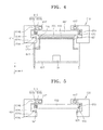
- FIG. 4 is a cross-sectional view of a first conveyer unit according to an embodiment of the present invention.
- FIG. 5 is a cross-sectional view of a second conveyer unit according to an embodiment of the present invention.
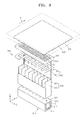
- FIG. 6 is a schematic perspective cutaway view of an organic layer deposition assembly of the organic layer deposition apparatus of FIG. 1 , according to an embodiment of the present invention
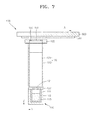
- FIG. 7 is a schematic sectional side view of the organic layer deposition assembly of FIG. 6 , according to an embodiment of the present invention.
- FIG. 8 is a schematic sectional view in an XZ plane of the organic layer deposition assembly of FIG. 6 , according to an embodiment of the present invention.
- FIG. 9 is a schematic perspective cutaway view of an organic layer deposition assembly according to another embodiment of the present invention.
- FIG. 10 is a schematic perspective view of an organic layer deposition assembly according to another embodiment of the present invention.
- FIG. 11 is a schematic perspective view of an organic layer deposition assembly according to another embodiment of the present invention.
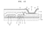
- FIG. 12 is a cross-sectional view of an active matrix organic light-emitting display device fabricated by using an organic layer deposition apparatus, according to an embodiment of the present invention.
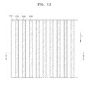
- FIG. 13 is a plan view of one or more organic layers on a substrate, according to an embodiment of the present invention.
- FIG. 14 is a cross-sectional view of the one or more layers on the substrate taken along line I-I of FIG. 13 , according to an embodiment of the present invention.
- FIG. 1 is a schematic structure view of an organic layer deposition apparatus according to an embodiment of the present invention.
- FIG. 2 illustrates a modified example of the organic layer deposition apparatus of FIG. 1.
- FIG. 3 is a view of an example of an electrostatic chuck 600.
- the organic layer deposition apparatus includes a loading unit 710, a deposition unit 730, an unloading unit 720, a first conveyer unit 610, and a second conveyer unit 620.
- the loading unit 710 may include a first rack 712, a transport robot 714, a transport chamber 716, and a first inversion chamber 718.
- a plurality of substrates 500 onto which a deposition material is not applied are stacked up on the first rack 712.
- the transport robot 714 picks up one of the substrates 500 from the first rack 712, disposes it on the electrostatic chuck 600 transferred by the second conveyer unit 620, and moves the electrostatic chuck 600 on which the substrate 500 is disposed into the transport chamber 716.
- the first inversion chamber 718 is disposed adjacent to the transport chamber 716.
- the first inversion chamber 718 includes a first inversion robot 719 that inverts the electrostatic chuck 600 and then loads it onto the first conveyer unit 610 of the deposition unit 730.
- the electrostatic chuck 600 may include an electrode 602 embedded in a main body 601 of the electrostatic chuck 600.
- the main body 601 is formed of ceramic, and the electrode 602 is supplied with power.
- the electrostatic chuck 600 may fix the substrate 500 on a surface of the main body 601 as a high voltage is applied to the electrode 602.
- the transport robot 714 places one of the substrates 500 on the surface of the electrostatic chuck 600, and the electrostatic chuck 600 on which the substrate 500 is disposed is loaded into the transport chamber 716.
- the first inversion robot 719 inverts the electrostatic chuck 600 so that the substrate 500 is turned upside down in the deposition unit 730.
- the unloading unit 720 is constituted to operate in an opposite manner to the loading unit 710 described above. Specifically, a second inversion robot 729 in a second inversion chamber 728 inverts the electrostatic chuck 600, which has passed through the deposition unit 730 while the substrate 500 is disposed on the electrostatic chuck 600, and then moves the electrostatic chuck 600 on which the substrate 500 is disposed into an ejection chamber 726. Then, an ejection robot 724 removes the electrostatic chuck 600 on which the substrate 500 is disposed from the ejection chamber 726, separates the substrate 500 from the electrostatic chuck 600, and then loads the substrate 500 onto the second rack 722. The electrostatic chuck 600 separated from the substrate 500 is returned back into the loading unit 710 via the second conveyer unit 620.
- the present invention is not limited to the above description.
- the substrate 500 when disposing the substrate 500 on the electrostatic chuck 600, the substrate 500 may be fixed onto a bottom surface of the electrostatic chuck 600 and then moved into the deposition unit 730.
- the first inversion chamber 718 and the first inversion robot 719, and the second inversion chamber 728 and the second inversion robot 729 are not used.
- the deposition unit 730 may include at least one deposition chamber. As illustrated in FIG. 1 , the deposition unit 730 may include a first chamber 731. In the embodiment illustrated in FIG. 1 , first to four organic layer deposition assemblies 100, 200, 300, and 400 may be disposed in the first chamber 731. Although FIG. 1 illustrates that a total of four organic layer deposition assemblies, i.e., the first to fourth organic layer deposition assemblies 100 to 400, are installed in the first chamber 731, the total number of organic layer deposition assemblies that may be installed in the first chamber 731 may vary according to the deposition material and deposition conditions. The first chamber 731 is maintained in a vacuum state during a deposition process.
- a deposition unit 730 may include the first chamber 731 and a second chamber 732 that are connected to each other.
- the first and second organic layer deposition assemblies 100 and 200 may be disposed in the first chamber 731, and the third and fourth organic layer deposition assemblies 300 and 400 may be disposed in the second chamber 732.
- the organic layer deposition system may include more than two chambers.
- the electrostatic chuck 600 on which the substrate 500 is disposed may be moved at least to the deposition unit 730 or may be moved sequentially to the loading unit 710, the deposition unit 730, and the unloading unit 720, by the first conveyer unit 610.
- the electrostatic chuck 600 that is separated from the substrate 500 in the unloading unit 720 is moved back to the loading unit 710 by the second conveyer unit 620.
- FIG. 4 is a cross-sectional view of the first conveyer unit 610, according to an embodiment of the present invention.
- the first conveyer unit 610 moves the electrostatic chuck 600 that is fixedly supporting the substrate.
- the first conveyer unit 610 may include a frame 611, a lower plate 613, a first guide unit 614, and a sheet support 615.
- the frame 611 forms a base of the first conveyer unit 610.
- the frame 611 may be substantially in the form of an empty box.
- the lower plate 613 forms a lower side of the frame 611.
- a deposition source 10 may be disposed on the lower plate 613.
- the frame 611 and the lower plate 613 may be formed as separate units, which may then be combined together.
- the frame 611 and the lower plate 613 are integrally (originally) formed as one body.
- the lower plate 613 with the deposition source 10 thereon may be formed as a cassette-like structure to be withdrawn out of the frame 611, which may facilitate replacement of the deposition source 10.
- the sheet support 615 may be formed to protrude from an inner sidewall of the frame 611.
- the sheet support 615 may support a patterning slit sheet 150.
- the sheet support 615 may guide a deposition material discharged through deposition source nozzles to move straight, and not to flow in the X-axis direction.
- the first guide unit 614 may be disposed on the frame 611, and may guide the electrostatic chuck 600 to move in a direction.
- the first guide unit 614 is disposed to pass through the first chamber 731 of the deposition unit 730.
- the first guide unit 614 receives the opposite edges of the electrostatic chuck 600 to guide the movement of the electrostatic chuck 600.
- the first guide unit 614 may include two first receiving members 614a and two second receiving members 614b respectively disposed under and above the electrostatic chuck 600 at the two opposite lateral portions of the electrostatic chuck 600, and two connection members 614c respectively connecting each of the the first receiving members 614a with the respective second receiving member 614b.
- the first receiving member 614a, the second receiving member 614b, and the connection member 614c together define a receiving groove 614d at each side of the electrostatic chuck 600. Two opposite sides of the electrostatic chuck 600 are each accommodated in a receiving groove 614d so that the electrostatic chuck 600 is moved along the two receiving grooves 614d.
- a driving unit 616 is disposed at a side of the connection member 614c in the receiving groove 614d to correspond to one side of the electrostatic chuck 600, and a side magnetic levitation bearing 618 is disposed to correspond to the other side of the electrostatic chuck 600 opposite to (facing oppositely way from) the driving unit 616.
- the side magnetic levitation bearing 618 includes a magnet selected from the group consisting of electromagnets, permanent magnets, superconducting magnets, and combinations thereof.
- the driving unit 616 may be a linear motor.
- Linear motors have a low friction coefficient relative to existing sliding guide systems and a very high level of position spotting with almost no positional error.
- a linear motor acting as the driving unit 616 may include a coil 616a and a magnetic rail 616b.
- the coil 616a is disposed on one side of the connection member 614c of the first guide unit 614, and the magnetic rail 616b is disposed at a side of the electrostatic chuck 600 to correspond to the coil 616a. Since the magnetic rail 616b, not the coil 616a, is disposed on the moving electrostatic chuck 600, the electrostatic chuck 600 may be driven without applying power.
- the side magnetic levitation bearing 618 is disposed at (on) the connection member 614c of the first guide unit 614 to correspond to the other side of the electrostatic chuck 600 opposite to the driving unit 616.
- the side magnetic levitation bearing 618 provides a gap between the electrostatic chuck 600 and the first guide unit 614, thereby allowing the electrostatic chuck 600 to move not in contact with and along the first guide unit 614.
- An upper (top) magnetic levitation bearing 617 may be disposed on the second receiving member 614b to be above the electrostatic chuck 600.
- the upper magnetic levitation bearing 617 enables the electrostatic chuck 600 to move along the first guide unit 614 not to contact the first receiving member 614a and the second receiving member 614b with a constant interval therefrom.
- a magnetic levitation bearing may be disposed at (on) the first receiving member 614a to correspond to a bottom side of the electrostatic chuck 600.
- the upper magnetic levitation bearing 617 includes a magnet selected from the group consisting of electromagnets, permanent magnets, superconducting magnets, and combinations thereof.
- the first guide unit 614 may further include a gap sensor 621.
- the gap sensor 621 may measure a gap between the electrostatic chuck 600 and the first guide unit 614. Referring to FIG. 4 , the gap sensor 621 may be disposed on the first receiving member 614a to correspond to a bottom side of the electrostatic chuck 600. The gap sensor 621 on the first receiving member 614a may measure a gap between the first receiving member 614a and the electrostatic chuck 600.
- a second gap sensor 622 may be disposed on the side magnetic levitation bearing 618. The second gap sensor 622 disposed on the side magnetic levitation bearing 618 may measure a gap between a side of the electrostatic chuck 600 and the side magnetic levitation bearing 618. However, aspects of the present invention are not limited thereto. The second gap sensor 622 may be disposed on the connection member 614c.
- Magnetic forces of the upper and side magnetic levitation bearings 617 and 618 are changed according to the gaps measured by the first and second gap sensors 621 and 622, thereby adjusting in real time a gap between the electrostatic chuck 600 and the first guide unit 614.
- the electrostatic chuck 600 may be precisely moved by a feedback control using the upper (top) and side magnetic levitation bearings 617 and 618 and the gap sensors 621 and 622.
- FIG. 5 is a cross-sectional view of the second conveyer unit 620, according to an embodiment of the present invention.
- the second conveyer unit 620 may include a second guide unit 634 for moving the electrostatic chuck 600 from which the substrate 500 has been removed.
- the second guide unit 634 may include a first receiving member 614a, a second receiving member 614b, and a connection member 614c.
- the electrostatic chuck 600 is accommodated in receiving grooves 614d defined by the first receiving member 614a, the second receiving member 614b, and the connection member 614c, and is moved along the receiving grooves 614d.
- the driving unit 616 is disposed at (on) the connection member 614c to correspond to one side of the electrostatic chuck 600.
- the driving unit 616 generates a driving force for moving the electrostatic chuck 600 along the second guide unit 634.
- the driving unit 616 may be a linear motor, which may include a coil 616a disposed on the connection member 614c and a magnetic rail 616b disposed on one side of the electrostatic chuck 600 to correspond to the coil 616a.
- the side magnetic levitation bearing 618 is disposed at (on) the connection member 614c of the first guide unit 614 to correspond to the other side of the electrostatic chuck 600 opposite to the driving unit 616.
- the upper magnetic levitation bearing 617 may be disposed at (on) the second receiving member 614b to be above the electrostatic chuck 600.
- the upper (top) and side magnetic levitation bearings 617 and 618 provide a gap between the electrostatic chuck 600 and the first guide unit 614, thereby allowing the electrostatic chuck 600 to move not in contact with and along the first guide unit 614.
- the second conveyer unit 620 may further include first and second gap sensors 621 and 622 for measuring a gap between the electrostatic chuck 600 and the second guide unit 634.
- the first gap sensor 621 may be disposed at (on) the first receiving member 614a to correspond to a bottom side of the electrostatic chuck 600.
- the second gap sensor 622 may be disposed on the side magnetic levitation bearing 618 to correspond to a side of the electrostatic chuck 600.
- FIG. 6 is a schematic perspective cutaway view of the organic layer deposition assembly 100 of the organic layer deposition apparatus of FIG. 1
- FIG. 7 is a cross-sectional side view of the organic layer deposition assembly 100 illustrated in FIG. 6
- FIG. 8 is a cross-sectional plan view of the organic layer deposition assembly 100 illustrated in FIG. 6 .
- the organic layer deposition assembly 100 includes a deposition source 110, a deposition source nozzle unit 120, a barrier plate assembly 130, and a patterning slit sheet 150.
- all the components of the organic layer deposition assembly 100 may be disposed within a chamber that is maintained at an appropriate degree of vacuum.
- the chamber is maintained at an appropriate vacuum in order to allow a deposition material to move substantially in a straight line in the organic layer deposition assembly 100.
- the substrate 500 which constitutes a deposition target on which the deposition material 115 is to be deposited, is transferred by the electrostatic chuck 600.
- the substrate 500 may be a substrate for flat panel displays.
- a large substrate, such as a mother glass, for manufacturing a plurality of flat panel displays, may be used as the substrate 500.
- the substrate 500 or the organic layer deposition assembly 100 may be moved relative to the other.
- the substrate 500 may be moved in a direction of an arrow A, relative to the organic layer deposition assembly 100.
- the size of the FMM is greater than or equal to the size of a substrate.
- the size of the FMM has to be increased when performing deposition on a larger substrate.
- deposition may be performed while the organic layer deposition assembly 100 or the substrate 500 is moved relative to the other.
- deposition may be continuously performed while the substrate 500, which is disposed such as to face the organic layer deposition assembly 100, is moved in a Y-axis direction.
- the deposition is performed in a scanning manner while the substrate 500 is moved in a direction of arrow A in FIG. 6 .
- the substrate 500 is illustrated as being moved in the Y-axis direction in FIG. 6 in the chamber 731 ( FIG. 1 ) when deposition is performed, the present invention is not limited thereto.
- Deposition may be performed while the organic layer deposition assembly 100 is moved in the Y-axis direction, while the substrate 500 is fixed.
- the patterning slit sheet 150 may be significantly smaller than an FMM used in a conventional deposition method.
- deposition is continuously performed, i.e., in a scanning manner while the substrate 500 is moved in the Y-axis direction.
- a length of the patterning slit sheet 150 in the Y-axis direction may be significantly less than a length of the substrate 500 in the Y-axis direction.
- a width of the patterning slit sheet 150 in the X-axis direction and a width of the substrate 500 in the X-axis direction are substantially equal to each other.
- deposition may be performed on the entire substrate 500 in a scanning manner while the substrate 500 or the organic layer deposition assembly 100 is moved relative to the other.
- the patterning slit sheet 150 may be formed to be significantly smaller than an FMM used in a conventional deposition method, it is relatively easy to manufacture the patterning slit sheet 150 used in the present invention.
- using the patterning slit sheet 150, which is smaller than an FMM used in a conventional deposition method is more convenient in all processes, including etching and other subsequent processes, such as precise extension, welding, moving, and cleaning processes, compared to the conventional deposition method using the larger FMM. This is more advantageous for manufacturing a relatively large display device.
- the organic layer deposition assembly 100 and the substrate 500 may be separated from each other by a set or predetermined distance. This will be described later in more detail.
- the deposition source 110 that contains and heats the deposition material 115 is disposed at a side of the chamber opposite to a side at which the substrate 500 is disposed.
- the deposition source 110 includes a crucible 112 that is filled with the deposition material 115, and a cooling block 111 surrounding the crucible 112.
- the cooling block 111 reduces or prevents radiation of heat from the crucible 112 to the outside, i.e., into the chamber (e.g., the chamber 731 and/or the chamber 732).
- the cooling block 111 may include a heater that heats the crucible 112.
- the deposition source nozzle unit 120 is disposed at a side of the deposition source 110, and in particular, at the side of the deposition source 110 facing the substrate 500.
- the deposition source nozzle unit 120 includes a plurality of deposition source nozzles 121 arranged at equal intervals in the X-axis direction.
- the deposition material 115 that is vaporized in the deposition source 110 passes through the deposition source nozzles 121 of the deposition source nozzle unit 120 towards the substrate 500, which is a deposition target on which the deposition material 115 is to be deposited.
- the barrier plate assembly 130 is disposed at a side of the deposition source nozzle unit 120 facing the substrate 500.
- the barrier plate assembly 130 includes a plurality of barrier plates 131, and a barrier plate frame 132 that covers sides of the barrier plates 131.
- the plurality of barrier plates 131 may be arranged parallel to each other at equal intervals in the X-axis direction.
- each of the barrier plates 131 may be arranged parallel to an YZ plane in FIG. 4 , and may have a rectangular shape.
- the deposition space is divided by the barrier plates 131 into the sub-deposition spaces S that respectively correspond to the deposition source nozzles 121 through which the deposition material 115 is discharged.
- the barrier plates 131 may be respectively disposed between adjacent deposition source nozzles 121.
- each of the deposition source nozzles 121 may be disposed between two adjacent barrier plates 131.
- the deposition source nozzles 121 may be respectively located at the midpoint between two adjacent barrier plates 131.
- the present invention is not limited to this structure.
- a plurality of deposition source nozzles 121 may be disposed between two adjacent barrier plates 131.
- the deposition source nozzles 121 may be also respectively located at the midpoint between two adjacent barrier plates 131.
- the barrier plates 131 partition the space between the deposition source nozzle unit 120 and the patterning slit sheet 150 into the plurality of sub-deposition spaces S, the deposition material 115 discharged through each of the deposition source nozzles 121 is not mixed with the deposition material 115 discharged through the other deposition source nozzles slits 121, and passes through the patterning slits 151 so as to be deposited on the substrate 500.
- the barrier plates 131 guide the deposition material 115, which is discharged through the deposition source nozzles 121, to move straight, i.e., to flow in the Z-axis direction.
- the deposition material 115 is forced or guided to move straight by installing the barrier plates 131, so that a smaller shadow zone may be formed on the substrate 500, compared to a case where no barrier plates are installed.
- the organic layer deposition assembly 100 and the substrate 500 may be separated from each other by a set or predetermined distance, as will be described later in detail.
- the patterning slit sheet 150 and a frame 155 in which the patterning slit sheet 150 is bound are disposed between the deposition source 110 and the substrate 500.
- the frame 155 may be formed to have a lattice shape, similar to a window frame.
- the patterning slit sheet 150 includes a plurality of patterning slits 151 arranged in the X-axis direction.
- the patterning slits 151 extend in the Y-axis direction.
- the deposition material 115 that has been vaporized in the deposition source 110 and passed through the deposition source nozzle 121, passes through the patterning slits 151 towards the substrate 500.
- the patterning slit sheet 150 may be formed of a metal thin film.
- the patterning slit sheet 150 is fixed to the frame 155 such that a tensile force is exerted thereon.
- the patterning slits 151 may be formed by etching the patterning slit sheet 150 to have a stripe pattern.
- the number of patterning slits 151 may be equal to the number of deposition patterns to be formed on the substrate 500.
- barrier plate assembly 130 and the patterning slit sheet 150 may be disposed to be separated from each other by a set or predetermined distance.
- the barrier plate assembly 130 and the patterning slit sheet 150 may be connected by (via) a connection member 135.
- the organic layer deposition assembly 100 performs deposition while being moved relative to the substrate 500.
- the patterning slit sheet 150 may be spaced apart from the substrate 500 by a set or predetermined distance.
- the barrier plates 131 are arranged between the deposition source nozzle unit 120 and the patterning slit sheet 150 to force or guide the deposition material 115 to move in a straight direction.
- a typical deposition method using an FMM deposition is performed with the FMM in close contact with a substrate in order to prevent formation of a shadow zone on the substrate.
- the contact may cause defects, such as scratches on patterns formed on the substrate.
- the size of the mask has to be the same as the size of the substrate since the mask may not be moved relative to the substrate.
- the size of the mask has to be increased as display devices become larger.
- the patterning slit sheet 150 is disposed to be spaced apart from the substrate 500 by a set or predetermined distance, which may be facilitated by installing the barrier plates 131 to reduce the size of the shadow zone formed on the substrate 500. Shadow zones on the substrate 500 may be reduced or minimized by installing the barrier plates 131.
- Thin films such as organic layers (refer to the organic layer 63 in FIG. 12 ) of an organic light-emitting display device may be formed using any suitable organic layer deposition apparatus having the structure described above.
- FIG. 9 is a schematic perspective cutaway view of an organic layer deposition assembly 800 according to another embodiment of the present invention.
- the organic layer deposition assembly 800 includes a deposition source 810, a deposition source nozzle unit 820, a first barrier plate assembly 830, a second barrier plate assembly 840, and a patterning slit sheet 850. Structures of the deposition source 810, the first barrier plate assembly 830, and the patterning slit sheet 850 are the same as those in the embodiment described with reference to FIG. 6 , and thus a detailed description thereof will not be provided here.
- the current embodiment differs from the previous embodiment in that the second barrier plate assembly 840 is disposed at a side of the first barrier plate assembly 830.
- the second barrier plate assembly 840 includes a plurality of second barrier plates 841, and a second barrier plate frame 842 that covers sides of the second barrier plates 841.
- the plurality of second barrier plates 841 may be arranged parallel to each other at equal intervals in the X-axis direction.
- each of the second barrier plates 841 may be formed to extend parallel to the YZ plane in FIG. 9 , i.e., perpendicular to the X-axis direction.
- the deposition space is divided by the first barrier plates 831 and the second barrier plates 841 into sub-deposition spaces that respectively correspond to the deposition source nozzles 821 through which the deposition material 115 is discharged.
- the second barrier plates 841 may be disposed to correspond respectively to the first barrier plates 831.
- the second barrier plates 841 may be respectively disposed to be parallel to and to be on the same plane as the first barrier plates 831.
- Each pair of the corresponding first and second barrier plates 831 and 841 may be located on the same plane.
- the first barrier plates 831 and the second barrier plates 841 are respectively illustrated as having the same thickness in the X-axis direction, aspects of the present invention are not limited thereto.
- the second barrier plates 841 which need to be accurately aligned with the patterning slits 851, may be formed to be relatively thin, whereas the first barrier plates 831, which do not need to be precisely aligned with the patterning slits 151, may be formed to be relatively thick. This makes it easier to manufacture the organic layer deposition assembly.
- FIG. 10 is a schematic perspective view of an organic layer deposition assembly 900 according to another embodiment of the present invention.
- the organic layer deposition assembly 900 includes a deposition source 910, a deposition source nozzle unit 920, and a patterning slit sheet 950.
- the deposition source 910 includes a crucible 912 that is filled with the deposition material 915, a cooling block 911 surrounding the crucible 912, and a heater that may be in the cooling block 911.
- the heater heats the crucible 912 to vaporize the deposition material 915, which is contained in the crucible 912, so as to move the vaporized deposition material 915 to the deposition source nozzle unit 920.
- the deposition source nozzle unit 920 which has a planar shape, is disposed at a side of the deposition source 910.
- the deposition source nozzle unit 920 includes a plurality of deposition source nozzles 921 arranged in the Y-axis direction.
- the patterning slit sheet 950 and a frame 955 are further disposed between the deposition source 910 and the substrate 500.
- the patterning slit sheet 950 includes a plurality of patterning slits 951 arranged in the X-axis direction.
- the deposition source 910 and the deposition source nozzle unit 920 may be connected to the patterning slit sheet 950 by a connection member 935.
- the current embodiment of FIG. 10 differs from the previous embodiments in the arrangement of the plurality of deposition source nozzles in the deposition source nozzle unit 920, which will now be described in more detail.
- the deposition source nozzle unit 920 is disposed at a side of the deposition source 910, and in particular, at the side of the deposition source 910 facing the substrate 500.
- the deposition source nozzle unit 920 includes a plurality of deposition source nozzles 921 arranged at equal intervals in the Y-axis direction, i.e., a scanning direction of the substrate 500.
- the deposition material 915 that is vaporized in the deposition source 910 passes through the deposition source nozzle unit 920 towards the substrate 500.
- the deposition source nozzle unit 920 includes the plurality of deposition source nozzles 921 arranged in the Y-axis direction, that is, the scanning direction of the substrate 500, the size of a pattern formed of the deposition material discharged through the patterning slits 951 of the patterning slit sheet 950 is affected by the size of one of the deposition source nozzles 921 (since there is only one line of deposition nozzles in the X-axis direction), and thus no shadow zone may be formed on the substrate 500.
- the plurality of deposition source nozzles 921 are arranged in the scanning direction of the substrate 500, even when there is a difference in flux between the deposition source nozzles 921, the difference may be compensated for and deposition uniformity may be maintained constant.
- FIG. 11 is a schematic perspective view of an organic layer deposition assembly 900' according to another embodiment of the present invention.
- the organic layer deposition apparatus 900' according to the current embodiment includes a deposition source 910, a deposition source nozzle unit 920, and a patterning slit sheet 950.
- the current embodiment differs from the previous embodiments in that a plurality of deposition source nozzles 921 formed in the deposition source nozzle unit 920 are tilted at a set or predetermined angle.
- the deposition source nozzles 921 may include deposition source nozzles 921 a and 921 b arranged in respective rows.
- the deposition source nozzles 921 a and 921 b may be arranged in respective rows to alternate in a zigzag pattern.
- the deposition source nozzles 921 a and 921 b may be tilted by a set or predetermined angle with respect to an XZ plane.
- the deposition source nozzles 921 a and 921 b are arranged to be tilted by a set or predetermined angle with respect to each other.
- the deposition source nozzles 921 a of a first row and the deposition source nozzles 921 b of a second row may be tilted towards each other.
- the deposition source nozzles 921 a of the first row in a left part of the deposition source nozzle unit 920 may be tilted towards a right side portion of the patterning slit sheet 950
- the deposition source nozzles 921 b of the second row in a right part of the deposition source nozzle unit 920 may be tilted towards a left side portion of the patterning slit sheet 950.
- the deposition of the deposition material 915 may be adjusted to lessen a thickness variation between the center and the end portions of the substrate 500 and improve thickness uniformity of the deposition film. Moreover, utilization efficiency of the deposition material 915 may also be improved.
- FIG. 12 is a cross-sectional view of an active matrix organic light-emitting display device fabricated by using an organic layer deposition apparatus, according to an embodiment of the present invention.
- the active matrix organic light-emitting display device is formed on a substrate 500.
- the substrate 500 may be formed of a transparent material, for example, glass, plastic, or metal.
- a thin film transistor (TFT) 40, a capacitor 50, and an organic light-emitting diode (OLED) 60 are disposed on the insulating layer 31, as illustrated in FIG. 12 .
- the capacitor 50 includes a first capacitor electrode 51 and a second capacitor electrode 52.
- a semiconductor active layer 41 is formed on an upper surface of the insulating layer 31 in a set or predetermined pattern.
- a gate insulating layer 32 is formed to cover the semiconductor active layer 41.
- the semiconductor active layer 41 may include a p-type or n-type semiconductor material.
- a gate electrode 42 of the TFT 40 is formed in a region of the gate insulating layer 32 corresponding to the semiconductor active layer 41.
- An interlayer insulating layer 33 is formed to cover the gate electrode 42.
- the interlayer insulating layer 33 and the gate insulating layer 32 are etched by, for example, dry etching, to form a contact hole exposing parts of the semiconductor active layer 41.
- the interlayer insulating layer 33 is formed (patterned) to be between the first capacitor electrode 51 and the second capacitor electrode 52.
- a source/drain electrode 43 is formed on the interlayer insulating layer 33 to contact the semiconductor active layer 41 through the contact hole.
- a passivation layer 34 is formed to cover the source/drain electrode 43, and is etched to expose a part of the drain electrode 43.
- a further insulating layer (not shown) may be formed on the passivation layer 34 so as to planarize the passivation layer 34.
- the OLED 60 displays a predetermined image information by emitting red, green, or blue light according to the current flowing through the OLED 60.
- the OLED 60 includes a first electrode 61 disposed on the passivation layer 34.
- the first electrode 61 is electrically connected to the drain electrode 43 of the TFT 40.
- a pixel defining layer 35 is formed to cover the first electrode 61.
- An opening 65 is formed in the pixel defining layer 35, and then an organic layer 63, including an emission layer, is formed in a region defined by the opening 65.
- a second electrode 62 is formed on the organic layer 63.
- the pixel defining layer 35 which defines individual pixels, is formed of an organic material.
- the pixel defining layer 35 also planarizes the surface of a region of the substrate 30 in which the first electrode 61 is formed, and in particular, the surface of the passivation layer 34.
- the first electrode 61 and the second electrode 62 are insulated from each other, and respectively apply voltages of opposite polarities to the organic layer 63, including the emission layer, to induce light emission.
- the organic layer 63 including an emission layer (EML) may be formed of a low-molecular weight organic material or a high-molecular weight organic material.
- the organic layer 63 (including the emission layer) may have a single or multi-layer structure including at least one selected from the group consisting of a hole injection layer (HIL), a hole transport layer (HTL), the emission layer (EML), an electron transport layer (ETL), and an electron injection layer (EIL).
- HIL hole injection layer
- HTL hole transport layer
- EML electron transport layer
- EIL electron injection layer
- Examples of available organic materials may include copper phthalocyanine (CuPc), N,N'-di(naphthalene-1-yl)-N,N'-diphenyl-benzidine (NPB), tris-8-hydroxyquinoline aluminum (Alq3), and the like.
- CuPc copper phthalocyanine
- NPB N,N'-di(naphthalene-1-yl)-N,N'-diphenyl-benzidine
- Alq3 tris-8-hydroxyquinoline aluminum
- the second electrode 62 may be formed by the same deposition method as used to form the organic layer 63.
- the first electrode 61 may function as an anode, and the second electrode 62 may function as a cathode. Alternatively, the first electrode 61 may function as a cathode, and the second electrode 62 may function as an anode.
- the first electrode 61 may be patterned to correspond to individual pixel regions, and the second electrode 62 may be formed to cover all the pixels.
- the first electrode 61 may be formed as a transparent electrode or a reflective electrode.
- the transparent electrode may be formed of indium tin oxide (ITO), indium zinc oxide (IZO), zinc oxide (ZnO), and/or indium oxide (In 2 O 3 ).
- the reflective electrode may be formed by forming a reflective layer from silver (Ag), magnesium (Mg), aluminum (AI), platinum (Pt), palladium (Pd), gold (Au), nickel (Ni), neodymium (Nd), iridium (lr), chromium (Cr), or a compound thereof, and forming a layer of ITO, IZO, ZnO, and/or In 2 O 3 on the reflective layer.
- the first electrode 61 may be formed by forming a layer by, for example, sputtering, and then patterning the layer by, for example, photolithography.
- the second electrode 62 may also be formed as a transparent electrode or a reflective electrode.
- the second electrode 62 functions as a cathode.
- a transparent electrode may be formed by depositing a metal having a low work function, such as lithium (Li), calcium (Ca), lithium fluoride/calcium (LiF/Ca), lithium fluoride/aluminum (LiF/AI), aluminum (AI), silver (Ag), magnesium (Mg), or a compound thereof on a surface of the organic layer 63, including an emission layer, and forming an auxiliary electrode layer or a bus electrode line thereon from ITO, IZO, ZnO, In 2 O 3 , or the like.
- a metal having a low work function such as lithium (Li), calcium (Ca), lithium fluoride/calcium (LiF/Ca), lithium fluoride/aluminum (LiF/AI), aluminum (AI), silver (Ag), magnesium (Mg), or a compound thereof on a surface of the organic
- the reflective layer may be formed by depositing Li, Ca, LiF/Ca, LiF/AI, AI, Ag, Mg, or a compound thereof on the entire surface of the organic layer 63.
- the second electrode 62 may be formed by using the same deposition method as used to form the organic layer 63, including an emission layer, described above.
- a protective layer 64 may be further formed on the second electrode 62.
- the protective layer 64 formed on the second electrode 62 may serve as a mask in removing the organic layer 63 from non-pixel regions, and at the same time protect the second electrode 62.
- FIG. 13 is a plan view of one or more organic layers 63B, 63G, and 63R formed on a substrate 500, according to an embodiment of the present invention.
- the substrate 500 has a size of at least 40 inches, and an organic layer 63B, 63G, and 63R is formed to have a linear pattern. That is, the organic layer 63B, 63G, and 63R is formed to have a plurality of linear stripes including a first or blue (B) stripe 63B, a second or green (G) stripe 63G, and a third or red (R) stripe 63R.
- the linear pattern of the organic layer 63B, 63G, and 63R is formed using any suitable one of the above described organic layer deposition apparatuses according to embodiments of the present invention.
- the organic layer 63B, 63G, and 63R may include an emission layer (EML) for emitting a blue (B), green (G), or red (R) light.
- EML emission layer
- the first or blue (B) stripe 63B includes the emission layer (EML) for emitting blue light
- the second or green (G) stripe 63G includes the emission layer (EML) for emitting green light
- the third or red (R) stripe 63R includes the emission layer (EML) for emitting red light.
- each of the organic layers 63B, 63G, and 63R may further include a layer selected from the group consisting of a hole injection layer (HIL), a hole transport layer (HTL), an electron transport layer (ETL), an electron injection layer (EIL), and combinations thereof.
- HIL hole injection layer
- HTL hole transport layer
- ETL electron transport layer
- EIL electron injection layer
- FIG. 14 is a cross-sectional view of the one or more layers formed on the substrate taken along line I-I of FIG. 13 , according to an embodiment of the present invention.
- the organic layer is formed on the substrate 500 to have a non-uniform thickness. That is, a first portion P1 of the organic layer on the substrate 500 is shown to have a thickness or height of h1, a second portion P2 of the organic layer on the substrate 500 is shown to have a thickness or height of h2, a third portion P3 of the organic layer on the substrate 500 is shown to have a thickness or height of h3, a fourth portion P4 of the organic layer on the substrate 500 is shown to have a thickness or height of h4, and a fifth portion P5 of the organic layer on the substrate 500 is shown to have a thickness or height of h5.
- the thickness h1 is greater than h2, the thickness h2 is greater than the thickness h3, the thickness h3 is greater than the thickness h4, and the thickness h4 is greater than the thickness h5.
- the first, second, third, fourth, or fifth portion P1, P2, P3, P4, or P5 may be a cross-sectional portion of the first, second, or third stripe 63B, 63B, or 63R. That is, in one embodiment, the fifth portion P5 is the cross-sectional portion of the first stripe 63B, the fourth portion P4 is the cross-sectional portion of the second stripe 63G, and the third portion P3 is the cross-sectional portion of the third stripe 63R.
- the non-uniform thickness of the organic layer P1, P2, P3, P5, and P5 is formed using any suitable one of the above described organic layer deposition apparatuses according to embodiments of the present invention.
- the suitable organic layer deposition apparatus includes an organic layer deposition assembly that is composed to include a patterning slit sheet 150. That is, as shown in FIG. 14 , the patterning slit sheet 150 of the organic layer deposition assembly is utilized to form the organic layer on the substrate 500.
- the patterning slit sheet 150 is disposed to be spaced apart from the substrate 500 and is smaller than the substrate 500 in size.
- the patterning slit sheet 150 or the substrate 500 is configured to be moved relative to the other. As such, the organic layer is formed on the substrate 500 to have the linear pattern as shown in FIG. 13 , and/or is formed to have the non-uniform thickness as shown in FIG. 14
- the organic layer deposition apparatuses according to the embodiments of the present invention may be applied to form an organic layer or an inorganic layer of an organic TFT, and to form layers from various suitable materials.
- organic layer deposition apparatuses may be readily manufactured and may be simply applied to the manufacture of large-sized display devices on a mass scale.
- the organic layer deposition apparatuses may improve manufacturing yield and deposition efficiency.
Landscapes
- Chemical & Material Sciences (AREA)
- Engineering & Computer Science (AREA)
- Chemical Kinetics & Catalysis (AREA)
- Materials Engineering (AREA)
- Mechanical Engineering (AREA)
- Metallurgy (AREA)
- Organic Chemistry (AREA)
- Microelectronics & Electronic Packaging (AREA)
- Manufacturing & Machinery (AREA)
- Electroluminescent Light Sources (AREA)
- Physical Vapour Deposition (AREA)
- Container, Conveyance, Adherence, Positioning, Of Wafer (AREA)
Abstract
Description
- This application claims priority to and the benefit of Korean Patent Application No.
10-2011-0066124, filed on July 4, 2011 - Aspects of embodiments according to the present invention relate to an organic layer deposition apparatus and a method of manufacturing an organic light-emitting display device by using the same.
- Organic light-emitting display devices have a larger viewing angle, better contrast characteristics, and a faster response speed than other display devices, and thus have drawn attention as next-generation display devices.
- Organic light-emitting display devices generally have a stacked structure including an anode, a cathode, and an emission layer interposed between the anode and the cathode. The devices display images in color when holes and electrons, injected respectively from the anode and the cathode, recombine in the emission layer to emit light. However, it is difficult to achieve a high light-emission efficiency with such a structure, and thus intermediate layers, including an electron injection layer, an electron transport layer, a hole transport layer, a hole injection layer, and the like may be additionally interposed between the emission layer and each of the electrodes.
- Aspects of embodiments according to the present invention are directed toward an organic layer deposition apparatus that may be easily manufactured, that may be applied to the manufacture of large-size display devices on a mass scale in a simple fashion, and that improves manufacturing yield and deposition efficiency, and a method of manufacturing an organic light-emitting display device by using the organic layer deposition apparatus.
- According to an embodiment of the present invention, there is provided an organic layer deposition apparatus including: an electrostatic chuck for supporting a substrate; a deposition unit including a chamber for maintaining a vacuum and an organic layer deposition assembly for depositing at least one organic layer on the substrate supported by the electrostatic chuck; and a first conveyer unit passing through the chamber and for moving the electrostatic chuck supporting the substrate into the deposition unit, wherein the first conveyer unit includes a guide unit including a receiving member for supporting the electrostatic chuck to be movable in a direction while the electrostatic chuck is spaced apart from the first conveyer unit, and wherein the substrate is spaced apart from the organic layer deposition assembly, and the substrate or the organic layer deposition assembly is configured to be moved relative to the other during deposition.
- In one embodiment, the organic layer deposition apparatus further includes: a loading unit for fixing the substrate to the electrostatic chuck; and an unloading unit for separating the substrate on which deposition has been completed from the electrostatic chuck. The first conveyer unit may be configured to sequentially move the electrostatic chuck to the loading unit, the deposition unit, and the unloading unit. The organic layer deposition apparatus may further include a second conveyer unit for returning the electrostatic chuck separated from the substrate, from the unloading unit to the loading unit.
- In one embodiment, the guide unit includes: a driving unit for generating a driving force to move the electrostatic chuck; and a magnetic levitation bearing for levitating the electrostatic chuck above the receiving member to move without contacting the receiving member. The driving unit may include a linear motor. The linear motor may include a magnetic rail disposed at a side of the electrostatic chuck and a coil disposed in the receiving member. The magnetic levitation bearing may include a side magnetic levitation bearing disposed at a side of the electrostatic chuck, and an upper magnetic levitation bearing disposed on the electrostatic chuck, and the driving unit may be disposed at a side of the electrostatic chuck. The magnetic levitation bearing may include a magnet selected from the group consisting of electromagnets, permanent magnets, superconducting magnets, and combinations thereof.
- In one embodiment, the organic layer deposition apparatus further includes a gap sensor for measuring a gap interval between the receiving member and the electrostatic chuck. The organic layer deposition apparatus may further include a magnetic levitation bearing controlled by the gap sensor to provide a magnetic force for levitating the electrostatic chuck above the receiving member. The magnetic levitation bearing may include a side magnetic levitation bearing disposed at a side of the electrostatic chuck, and an upper magnetic levitation bearing disposed on the electrostatic chuck. The gap sensor may include a first gap sensor for measuring a gap interval between the electrostatic chuck and the first conveyer unit along a first direction, and a second gap sensor for measuring a gap interval between the electrostatic chuck and the first conveyer unit along a second direction crossing the first direction.
- In one embodiment, the organic layer deposition apparatus further includes: a first magnetic levitation bearing for levitating the electrostatic chuck to be spaced apart from the first conveyer unit along a first direction; and a second magnetic levitation bearing for levitating the electrostatic chuck to be spaced apart from the first conveyer unit along a second direction crossing the first direction.
- In one embodiment, the receiving member includes a receiving groove for receiving the opposite sides of the electrostatic chucks.
- In one embodiment, the organic layer deposition assembly includes a plurality of organic layer deposition assemblies disposed in the chamber.
- In one embodiment, the chamber includes a first chamber and a second chamber interconnected with each other, and the organic layer deposition assembly includes a plurality of organic layer deposition assemblies disposed in each of the first and second chamber.
- In one embodiment, the organic layer deposition assembly includes: a deposition source configured to discharge a deposition material; a deposition source nozzle unit disposed at a side of the deposition source and including a plurality of deposition source nozzles; and a patterning slit sheet disposed to face and spaced apart from the deposition source nozzle unit, having a plurality of patterning slits, and being smaller than the substrate.
- According to another embodiment of the present invention, there is provided an active matrix organic light-emitting display device including: the above substrate having a size of at least 40 inches; and the at least one organic layer on the substrate having a linear pattern formed using the above organic layer deposition apparatus.
- In one embodiment, the at least one organic layer includes an emission layer (EML). The at least one organic layer may further include a layer selected from the group consisting of a hole injection layer (HIL), a hole transport layer (HTL), an electron transport layer (ETL), an electron injection layer (EIL), and combinations thereof.
- In one embodiment, the at least one organic layer has a non-uniform thickness.
- According to another embodiment of the present invention, there is provided an active matrix organic light-emitting display device including: the at least one organic layer having a non-uniform thickness formed using the above organic layer deposition apparatus.
- According to another embodiment of the present invention, there is provided a method of manufacturing an organic light-emitting display device, the method including: supporting a substrate with an electrostatic chuck; conveying the electrostatic chuck supporting the substrate into a chamber maintained at a vacuum by using a first conveyer unit passing through the chamber; and depositing at least one organic layer on the substrate by using an organic layer deposition assembly disposed in the chamber while the substrate or the organic layer deposition assembly moves relative to the other, wherein the electrostatic chuck is moved with the first conveyer unit in the chamber while spaced apart from the first conveyer unit, and wherein the substrate is spaced apart from the organic layer deposition assembly.
- In one embodiment, the conveying of the electrostatic chuck includes levitating the electrostatic chuck to be spaced apart from the first conveyer unit. The conveying of the electrostaic chuck may include: generating a driving force by a driving unit to move the electrostatic chuck; and levitating the electrostatic chuck to move without contacting the first conveyer unit by a magnetic levitation bearing.
- In one embodiment, the conveying of the electrostatic chuck includes measuring a gap interval between the first conveyer unit and the electrostatic chuck by a gap sensor. The conveying of the electrostatic chuck may include: controlling a magnetic levitation bearing by the gap sensor to provide a magnetic force; and levitating the electrostatic chuck to move without contacting the first conveyer unit by the magnetic force. The magnetic levitation bearing may include a side magnetic levitation bearing disposed at a side of the electrostatic chuck, and an upper magnetic levitation bearing disposed on the electrostatic chuck. The measuring of the gap interval may include: measuring a gap interval between the electrostatic chuck and the first conveyer unit along a first direction by a first gap sensor; and measuring a gap interval between the electrostatic chuck and the first conveyer unit along a second direction crossing the first direction by a second gap sensor. The levitating of the electrostatic chuck to move without contacting the first conveyer unit by the magnetic force may include: levitating the electrostatic chuck to be spaced apart from the first conveyer unit along a first direction by a first magnetic levitation bearing; and levitating the electrostatic chuck to be spaced apart from the first conveyer unit along a second direction crossing the first direction by a second magnetic levitation bearing.
- In one embodiment, the method further includes, after the depositing of the organic layer: removing the substrate on which the deposition has been completed out of the chamber by using the first conveyer unit; separating the substrate from the electrostatic chuck; and returning the electrostatic chuck separated from the substrate to support another substrate with the electrostatic chuck by using a second conveyer unit disposed outside the chamber.
- In one embodiment, the deposition assembly includes a plurality of organic layer deposition assemblies disposed in the chamber, and the depositing is performed by using the plurality of organic layer deposition assemblies in sequence.
- In one embodiment, the chamber includes a first chamber and a second chamber interconnected with each other, and the organic layer deposition assembly includes a plurality of organic layer deposition assemblies disposed in each of the first and second chambers, wherein the depositing is continuously performed with the substrate moving between the first chamber and the second chamber.
- In one embodiment, the organic layer deposition assembly includes: a deposition source configured to discharge a deposition material; a deposition source nozzle unit disposed at a side of the deposition source and including a plurality of deposition source nozzles; and a patterning slit sheet disposed to face and spaced apart from the deposition source nozzle unit, having a plurality of patterning slits, and being smaller than the substrate.
- In one embodiment, the first conveyer unit includes: a guide unit including a receiving member for supporting the electrostatic chuck to be movable in a direction; a linear motor for generating a driving force to move the electrostatic chuck; and a magnetic levitation bearing for levitating the electrostatic chuck to be spaced apart from the receiving member. The linear motor may include a magnetic rail disposed at a side of the electrostatic chuck and a coil disposed in the receiving member. The magnetic levitation bearing may include a side magnetic levitation bearing disposed at a side of the electrostatic chuck, and an upper magnetic levitation bearing disposed on the electrostatic chuck, and the driving unit is disposed at a side of the electrostatic chuck.
- According to another embodiment of the present invention, there is provided an active matrix organic light-emitting display device including: the substrate having a size of at least 40 inches; and the at least one organic layer on the substrate having a linear pattern formed using the above method.
- According to another embodiment of the present invention, there is provided an active matrix organic light-emitting display device including: the at least one organic layer having a non-uniform thickness formed using the above method.
- The above and other features and aspects of the present invention will become more apparent by describing in detail exemplary embodiments thereof with reference to the attached drawing in which:
-
FIG. 1 is a schematic structure diagram of an organic layer deposition apparatus according to an embodiment of the present invention; -
FIG. 2 is a structure diagram of a modified example of the organic layer deposition apparatus ofFIG. 1 ; -
FIG. 3 is a view of an example of an electrostatic chuck; -
FIG. 4 is a cross-sectional view of a first conveyer unit according to an embodiment of the present invention; -
FIG. 5 is a cross-sectional view of a second conveyer unit according to an embodiment of the present invention; -
FIG. 6 is a schematic perspective cutaway view of an organic layer deposition assembly of the organic layer deposition apparatus ofFIG. 1 , according to an embodiment of the present invention; -
FIG. 7 is a schematic sectional side view of the organic layer deposition assembly ofFIG. 6 , according to an embodiment of the present invention; -
FIG. 8 is a schematic sectional view in an XZ plane of the organic layer deposition assembly ofFIG. 6 , according to an embodiment of the present invention; -
FIG. 9 is a schematic perspective cutaway view of an organic layer deposition assembly according to another embodiment of the present invention; -
FIG. 10 is a schematic perspective view of an organic layer deposition assembly according to another embodiment of the present invention; -
FIG. 11 is a schematic perspective view of an organic layer deposition assembly according to another embodiment of the present invention; and -
FIG. 12 is a cross-sectional view of an active matrix organic light-emitting display device fabricated by using an organic layer deposition apparatus, according to an embodiment of the present invention. -
FIG. 13 is a plan view of one or more organic layers on a substrate, according to an embodiment of the present invention. -
FIG. 14 is a cross-sectional view of the one or more layers on the substrate taken along line I-I ofFIG. 13 , according to an embodiment of the present invention. - Reference will now be made in detail to embodiments of the present invention, examples of which are illustrated in the accompanying drawings. The invention may, however, be embodied in many different forms and should not be construed as being limited to the embodiments set forth herein; rather, these embodiments are provided so that this disclosure will be thorough and complete, and will fully convey the concept of the invention to those skilled in the art.
-
FIG. 1 is a schematic structure view of an organic layer deposition apparatus according to an embodiment of the present invention.FIG. 2 illustrates a modified example of the organic layer deposition apparatus ofFIG. 1. FIG. 3 is a view of an example of anelectrostatic chuck 600. - Referring to
FIG. 1 , the organic layer deposition apparatus according to the current embodiment includes aloading unit 710, adeposition unit 730, anunloading unit 720, afirst conveyer unit 610, and asecond conveyer unit 620. - The
loading unit 710 may include afirst rack 712, atransport robot 714, atransport chamber 716, and afirst inversion chamber 718. - A plurality of
substrates 500 onto which a deposition material is not applied are stacked up on thefirst rack 712. Thetransport robot 714 picks up one of thesubstrates 500 from thefirst rack 712, disposes it on theelectrostatic chuck 600 transferred by thesecond conveyer unit 620, and moves theelectrostatic chuck 600 on which thesubstrate 500 is disposed into thetransport chamber 716. - The
first inversion chamber 718 is disposed adjacent to thetransport chamber 716. Thefirst inversion chamber 718 includes afirst inversion robot 719 that inverts theelectrostatic chuck 600 and then loads it onto thefirst conveyer unit 610 of thedeposition unit 730. - Referring to
FIG. 3 , theelectrostatic chuck 600 may include anelectrode 602 embedded in amain body 601 of theelectrostatic chuck 600. Here, themain body 601 is formed of ceramic, and theelectrode 602 is supplied with power. Theelectrostatic chuck 600 may fix thesubstrate 500 on a surface of themain body 601 as a high voltage is applied to theelectrode 602. - Referring back to
FIG. 1 , thetransport robot 714 places one of thesubstrates 500 on the surface of theelectrostatic chuck 600, and theelectrostatic chuck 600 on which thesubstrate 500 is disposed is loaded into thetransport chamber 716. Thefirst inversion robot 719 inverts theelectrostatic chuck 600 so that thesubstrate 500 is turned upside down in thedeposition unit 730. - The
unloading unit 720 is constituted to operate in an opposite manner to theloading unit 710 described above. Specifically, asecond inversion robot 729 in asecond inversion chamber 728 inverts theelectrostatic chuck 600, which has passed through thedeposition unit 730 while thesubstrate 500 is disposed on theelectrostatic chuck 600, and then moves theelectrostatic chuck 600 on which thesubstrate 500 is disposed into anejection chamber 726. Then, anejection robot 724 removes theelectrostatic chuck 600 on which thesubstrate 500 is disposed from theejection chamber 726, separates thesubstrate 500 from theelectrostatic chuck 600, and then loads thesubstrate 500 onto thesecond rack 722. Theelectrostatic chuck 600 separated from thesubstrate 500 is returned back into theloading unit 710 via thesecond conveyer unit 620. - However, the present invention is not limited to the above description. For example, when disposing the
substrate 500 on theelectrostatic chuck 600, thesubstrate 500 may be fixed onto a bottom surface of theelectrostatic chuck 600 and then moved into thedeposition unit 730. In this case, for example, thefirst inversion chamber 718 and thefirst inversion robot 719, and thesecond inversion chamber 728 and thesecond inversion robot 729 are not used. - The
deposition unit 730 may include at least one deposition chamber. As illustrated inFIG. 1 , thedeposition unit 730 may include afirst chamber 731. In the embodiment illustrated inFIG. 1 , first to four organiclayer deposition assemblies first chamber 731. AlthoughFIG. 1 illustrates that a total of four organic layer deposition assemblies, i.e., the first to fourth organiclayer deposition assemblies 100 to 400, are installed in thefirst chamber 731, the total number of organic layer deposition assemblies that may be installed in thefirst chamber 731 may vary according to the deposition material and deposition conditions. Thefirst chamber 731 is maintained in a vacuum state during a deposition process. - In the organic layer deposition apparatus illustrated in
FIG. 2 , adeposition unit 730 may include thefirst chamber 731 and asecond chamber 732 that are connected to each other. In the embodiment illustrated inFIG. 2 , the first and second organiclayer deposition assemblies first chamber 731, and the third and fourth organiclayer deposition assemblies second chamber 732. In other embodiments, the organic layer deposition system may include more than two chambers. - In the embodiment illustrated in
FIG. 1 , theelectrostatic chuck 600 on which thesubstrate 500 is disposed may be moved at least to thedeposition unit 730 or may be moved sequentially to theloading unit 710, thedeposition unit 730, and theunloading unit 720, by thefirst conveyer unit 610. Theelectrostatic chuck 600 that is separated from thesubstrate 500 in theunloading unit 720 is moved back to theloading unit 710 by thesecond conveyer unit 620. -
FIG. 4 is a cross-sectional view of thefirst conveyer unit 610, according to an embodiment of the present invention. - The
first conveyer unit 610 moves theelectrostatic chuck 600 that is fixedly supporting the substrate. Thefirst conveyer unit 610 may include aframe 611, alower plate 613, afirst guide unit 614, and asheet support 615. - The
frame 611 forms a base of thefirst conveyer unit 610. Theframe 611 may be substantially in the form of an empty box. Thelower plate 613 forms a lower side of theframe 611. Adeposition source 10 may be disposed on thelower plate 613. Theframe 611 and thelower plate 613 may be formed as separate units, which may then be combined together. In one embodiment, theframe 611 and thelower plate 613 are integrally (originally) formed as one body. - Although not illustrated, the
lower plate 613 with thedeposition source 10 thereon may be formed as a cassette-like structure to be withdrawn out of theframe 611, which may facilitate replacement of thedeposition source 10. - The
sheet support 615 may be formed to protrude from an inner sidewall of theframe 611. Thesheet support 615 may support apatterning slit sheet 150. Thesheet support 615 may guide a deposition material discharged through deposition source nozzles to move straight, and not to flow in the X-axis direction. - The
first guide unit 614 may be disposed on theframe 611, and may guide theelectrostatic chuck 600 to move in a direction. Thefirst guide unit 614 is disposed to pass through thefirst chamber 731 of thedeposition unit 730. - The
first guide unit 614 receives the opposite edges of theelectrostatic chuck 600 to guide the movement of theelectrostatic chuck 600. Thefirst guide unit 614 may include twofirst receiving members 614a and twosecond receiving members 614b respectively disposed under and above theelectrostatic chuck 600 at the two opposite lateral portions of theelectrostatic chuck 600, and twoconnection members 614c respectively connecting each of the thefirst receiving members 614a with the respective second receivingmember 614b. Thefirst receiving member 614a, the second receivingmember 614b, and theconnection member 614c together define a receivinggroove 614d at each side of theelectrostatic chuck 600. Two opposite sides of theelectrostatic chuck 600 are each accommodated in a receivinggroove 614d so that theelectrostatic chuck 600 is moved along the two receivinggrooves 614d. - A driving
unit 616 is disposed at a side of theconnection member 614c in the receivinggroove 614d to correspond to one side of theelectrostatic chuck 600, and a side magnetic levitation bearing 618 is disposed to correspond to the other side of theelectrostatic chuck 600 opposite to (facing oppositely way from) thedriving unit 616. In one embodiment, the side magnetic levitation bearing 618 includes a magnet selected from the group consisting of electromagnets, permanent magnets, superconducting magnets, and combinations thereof. - Here, the driving
unit 616 may be a linear motor. Linear motors have a low friction coefficient relative to existing sliding guide systems and a very high level of position spotting with almost no positional error. A linear motor acting as the drivingunit 616 may include acoil 616a and amagnetic rail 616b. Thecoil 616a is disposed on one side of theconnection member 614c of thefirst guide unit 614, and themagnetic rail 616b is disposed at a side of theelectrostatic chuck 600 to correspond to thecoil 616a. Since themagnetic rail 616b, not thecoil 616a, is disposed on the movingelectrostatic chuck 600, theelectrostatic chuck 600 may be driven without applying power. - The side magnetic levitation bearing 618 is disposed at (on) the
connection member 614c of thefirst guide unit 614 to correspond to the other side of theelectrostatic chuck 600 opposite to thedriving unit 616. The side magnetic levitation bearing 618 provides a gap between theelectrostatic chuck 600 and thefirst guide unit 614, thereby allowing theelectrostatic chuck 600 to move not in contact with and along thefirst guide unit 614. - An upper (top) magnetic levitation bearing 617 may be disposed on the second receiving
member 614b to be above theelectrostatic chuck 600. The upper magnetic levitation bearing 617 enables theelectrostatic chuck 600 to move along thefirst guide unit 614 not to contact the first receivingmember 614a and the second receivingmember 614b with a constant interval therefrom. Although not illustrated, a magnetic levitation bearing may be disposed at (on) the first receivingmember 614a to correspond to a bottom side of theelectrostatic chuck 600. In one embodiment, the upper magnetic levitation bearing 617 includes a magnet selected from the group consisting of electromagnets, permanent magnets, superconducting magnets, and combinations thereof. - The
first guide unit 614 may further include agap sensor 621. Thegap sensor 621 may measure a gap between theelectrostatic chuck 600 and thefirst guide unit 614. Referring toFIG. 4 , thegap sensor 621 may be disposed on the first receivingmember 614a to correspond to a bottom side of theelectrostatic chuck 600. Thegap sensor 621 on the first receivingmember 614a may measure a gap between the first receivingmember 614a and theelectrostatic chuck 600. Asecond gap sensor 622 may be disposed on the sidemagnetic levitation bearing 618. Thesecond gap sensor 622 disposed on the side magnetic levitation bearing 618 may measure a gap between a side of theelectrostatic chuck 600 and the sidemagnetic levitation bearing 618. However, aspects of the present invention are not limited thereto. Thesecond gap sensor 622 may be disposed on theconnection member 614c. - Magnetic forces of the upper and side
magnetic levitation bearings second gap sensors electrostatic chuck 600 and thefirst guide unit 614. Theelectrostatic chuck 600 may be precisely moved by a feedback control using the upper (top) and sidemagnetic levitation bearings gap sensors -
FIG. 5 is a cross-sectional view of thesecond conveyer unit 620, according to an embodiment of the present invention. - The
second conveyer unit 620 may include asecond guide unit 634 for moving theelectrostatic chuck 600 from which thesubstrate 500 has been removed. - The
second guide unit 634 may include afirst receiving member 614a, asecond receiving member 614b, and aconnection member 614c. Theelectrostatic chuck 600 is accommodated in receivinggrooves 614d defined by the first receivingmember 614a, the second receivingmember 614b, and theconnection member 614c, and is moved along the receivinggrooves 614d. - The driving
unit 616 is disposed at (on) theconnection member 614c to correspond to one side of theelectrostatic chuck 600. The drivingunit 616 generates a driving force for moving theelectrostatic chuck 600 along thesecond guide unit 634. The drivingunit 616 may be a linear motor, which may include acoil 616a disposed on theconnection member 614c and amagnetic rail 616b disposed on one side of theelectrostatic chuck 600 to correspond to thecoil 616a. - The side magnetic levitation bearing 618 is disposed at (on) the
connection member 614c of thefirst guide unit 614 to correspond to the other side of theelectrostatic chuck 600 opposite to thedriving unit 616. The upper magnetic levitation bearing 617 may be disposed at (on) the second receivingmember 614b to be above theelectrostatic chuck 600. The upper (top) and sidemagnetic levitation bearings electrostatic chuck 600 and thefirst guide unit 614, thereby allowing theelectrostatic chuck 600 to move not in contact with and along thefirst guide unit 614. - The
second conveyer unit 620 may further include first andsecond gap sensors electrostatic chuck 600 and thesecond guide unit 634. Thefirst gap sensor 621 may be disposed at (on) the first receivingmember 614a to correspond to a bottom side of theelectrostatic chuck 600. Thesecond gap sensor 622 may be disposed on the side magnetic levitation bearing 618 to correspond to a side of theelectrostatic chuck 600. - Hereinafter, an embodiment of the organic
layer deposition assembly 100 of the organic layer deposition apparatus described above will be described.FIG. 6 is a schematic perspective cutaway view of the organiclayer deposition assembly 100 of the organic layer deposition apparatus ofFIG. 1 ,FIG. 7 is a cross-sectional side view of the organiclayer deposition assembly 100 illustrated inFIG. 6 , andFIG. 8 is a cross-sectional plan view of the organiclayer deposition assembly 100 illustrated inFIG. 6 . - Referring to
FIGS. 6 to 8 , the organiclayer deposition assembly 100 according to the current embodiment of the present invention includes adeposition source 110, a depositionsource nozzle unit 120, abarrier plate assembly 130, and apatterning slit sheet 150. - Although a chamber is not illustrated in
FIGS. 6 to 8 for convenience of explanation, all the components of the organiclayer deposition assembly 100 may be disposed within a chamber that is maintained at an appropriate degree of vacuum. The chamber is maintained at an appropriate vacuum in order to allow a deposition material to move substantially in a straight line in the organiclayer deposition assembly 100. - In the
chamber 731 ofFIG. 1 in which the organiclayer deposition assembly 100 is disposed, thesubstrate 500, which constitutes a deposition target on which thedeposition material 115 is to be deposited, is transferred by theelectrostatic chuck 600. Thesubstrate 500 may be a substrate for flat panel displays. A large substrate, such as a mother glass, for manufacturing a plurality of flat panel displays, may be used as thesubstrate 500. - In an embodiment, the
substrate 500 or the organiclayer deposition assembly 100 may be moved relative to the other. For example, as illustrated inFIG. 6 , thesubstrate 500 may be moved in a direction of an arrow A, relative to the organiclayer deposition assembly 100. - In a conventional deposition method using a fine metal mask (FMM), the size of the FMM is greater than or equal to the size of a substrate. Thus, the size of the FMM has to be increased when performing deposition on a larger substrate. However, it is difficult to manufacture a large FMM and to extend an FMM to be accurately aligned with a pattern.
- To overcome this problem, in the organic
layer deposition assembly 100 according to the current embodiment of the present invention, deposition may be performed while the organiclayer deposition assembly 100 or thesubstrate 500 is moved relative to the other. In other words, deposition may be continuously performed while thesubstrate 500, which is disposed such as to face the organiclayer deposition assembly 100, is moved in a Y-axis direction. In other words, the deposition is performed in a scanning manner while thesubstrate 500 is moved in a direction of arrow A inFIG. 6 . Although thesubstrate 500 is illustrated as being moved in the Y-axis direction inFIG. 6 in the chamber 731 (FIG. 1 ) when deposition is performed, the present invention is not limited thereto. Deposition may be performed while the organiclayer deposition assembly 100 is moved in the Y-axis direction, while thesubstrate 500 is fixed. - Thus, in the organic
layer deposition assembly 100 according to the current embodiment of the present invention, thepatterning slit sheet 150 may be significantly smaller than an FMM used in a conventional deposition method. In other words, in the organiclayer deposition assembly 100, deposition is continuously performed, i.e., in a scanning manner while thesubstrate 500 is moved in the Y-axis direction. Thus, a length of thepatterning slit sheet 150 in the Y-axis direction may be significantly less than a length of thesubstrate 500 in the Y-axis direction. Here, a width of thepatterning slit sheet 150 in the X-axis direction and a width of thesubstrate 500 in the X-axis direction are substantially equal to each other. However, even when the width of thepatterning slit sheet 150 in the X-axis direction is less than the width of thesubstrate 500 in the X-axis direction, deposition may be performed on theentire substrate 500 in a scanning manner while thesubstrate 500 or the organiclayer deposition assembly 100 is moved relative to the other. - As described above, since the
patterning slit sheet 150 may be formed to be significantly smaller than an FMM used in a conventional deposition method, it is relatively easy to manufacture thepatterning slit sheet 150 used in the present invention. In other words, using thepatterning slit sheet 150, which is smaller than an FMM used in a conventional deposition method, is more convenient in all processes, including etching and other subsequent processes, such as precise extension, welding, moving, and cleaning processes, compared to the conventional deposition method using the larger FMM. This is more advantageous for manufacturing a relatively large display device. - In order to perform deposition while the organic
layer deposition assembly 100 or thesubstrate 500 is moved relative to the other as described above, the organiclayer deposition assembly 100 and thesubstrate 500 may be separated from each other by a set or predetermined distance. This will be described later in more detail. - The
deposition source 110 that contains and heats thedeposition material 115 is disposed at a side of the chamber opposite to a side at which thesubstrate 500 is disposed. - The
deposition source 110 includes acrucible 112 that is filled with thedeposition material 115, and acooling block 111 surrounding thecrucible 112. Thecooling block 111 reduces or prevents radiation of heat from thecrucible 112 to the outside, i.e., into the chamber (e.g., thechamber 731 and/or the chamber 732). Thecooling block 111 may include a heater that heats thecrucible 112. - The deposition
source nozzle unit 120 is disposed at a side of thedeposition source 110, and in particular, at the side of thedeposition source 110 facing thesubstrate 500. The depositionsource nozzle unit 120 includes a plurality ofdeposition source nozzles 121 arranged at equal intervals in the X-axis direction. Thedeposition material 115 that is vaporized in thedeposition source 110 passes through thedeposition source nozzles 121 of the depositionsource nozzle unit 120 towards thesubstrate 500, which is a deposition target on which thedeposition material 115 is to be deposited. - The
barrier plate assembly 130 is disposed at a side of the depositionsource nozzle unit 120 facing thesubstrate 500. Thebarrier plate assembly 130 includes a plurality ofbarrier plates 131, and abarrier plate frame 132 that covers sides of thebarrier plates 131. The plurality ofbarrier plates 131 may be arranged parallel to each other at equal intervals in the X-axis direction. In addition, each of thebarrier plates 131 may be arranged parallel to an YZ plane inFIG. 4 , and may have a rectangular shape. The plurality ofbarrier plates 131 arranged as described above, partition the space between the depositionsource nozzle unit 120 and thepatterning slit sheet 150 into a plurality of sub-deposition spaces S (seeFIG. 8 ). In the organiclayer deposition assembly 100 according to the current embodiment of the present invention, as illustrated inFIG. 5 , the deposition space is divided by thebarrier plates 131 into the sub-deposition spaces S that respectively correspond to thedeposition source nozzles 121 through which thedeposition material 115 is discharged. - The
barrier plates 131 may be respectively disposed between adjacent deposition source nozzles 121. In other words, each of thedeposition source nozzles 121 may be disposed between twoadjacent barrier plates 131. Thedeposition source nozzles 121 may be respectively located at the midpoint between twoadjacent barrier plates 131. However, the present invention is not limited to this structure. For example, a plurality ofdeposition source nozzles 121 may be disposed between twoadjacent barrier plates 131. In this case, thedeposition source nozzles 121 may be also respectively located at the midpoint between twoadjacent barrier plates 131. - As described above, since the
barrier plates 131 partition the space between the depositionsource nozzle unit 120 and thepatterning slit sheet 150 into the plurality of sub-deposition spaces S, thedeposition material 115 discharged through each of the deposition source nozzles 121 is not mixed with thedeposition material 115 discharged through the other deposition source nozzles slits 121, and passes through the patterning slits 151 so as to be deposited on thesubstrate 500. In other words, thebarrier plates 131 guide thedeposition material 115, which is discharged through thedeposition source nozzles 121, to move straight, i.e., to flow in the Z-axis direction. - As described above, the
deposition material 115 is forced or guided to move straight by installing thebarrier plates 131, so that a smaller shadow zone may be formed on thesubstrate 500, compared to a case where no barrier plates are installed. Thus, the organiclayer deposition assembly 100 and thesubstrate 500 may be separated from each other by a set or predetermined distance, as will be described later in detail. - The
patterning slit sheet 150 and aframe 155 in which thepatterning slit sheet 150 is bound are disposed between thedeposition source 110 and thesubstrate 500. Theframe 155 may be formed to have a lattice shape, similar to a window frame. Thepatterning slit sheet 150 includes a plurality of patterning slits 151 arranged in the X-axis direction. The patterning slits 151 extend in the Y-axis direction. Thedeposition material 115 that has been vaporized in thedeposition source 110 and passed through thedeposition source nozzle 121, passes through the patterning slits 151 towards thesubstrate 500. - The
patterning slit sheet 150 may be formed of a metal thin film. Thepatterning slit sheet 150 is fixed to theframe 155 such that a tensile force is exerted thereon. The patterning slits 151 may be formed by etching thepatterning slit sheet 150 to have a stripe pattern. The number of patterning slits 151 may be equal to the number of deposition patterns to be formed on thesubstrate 500. - In addition, the
barrier plate assembly 130 and thepatterning slit sheet 150 may be disposed to be separated from each other by a set or predetermined distance. Alternatively, thebarrier plate assembly 130 and thepatterning slit sheet 150 may be connected by (via) aconnection member 135. - As described above, the organic
layer deposition assembly 100 according to the current embodiment of the present invention performs deposition while being moved relative to thesubstrate 500. In order to move the organiclayer deposition assembly 100 relative to thesubstrate 500, thepatterning slit sheet 150 may be spaced apart from thesubstrate 500 by a set or predetermined distance. In addition, to prevent the formation of a relatively large shadow zone on thesubstrate 500 when thepatterning slit sheet 150 and thesubstrate 500 are spaced apart from each other, thebarrier plates 131 are arranged between the depositionsource nozzle unit 120 and thepatterning slit sheet 150 to force or guide thedeposition material 115 to move in a straight direction. Thus, the size of the shadow zone that may be formed on thesubstrate 500 is sharply reduced. - In a typical deposition method using an FMM, deposition is performed with the FMM in close contact with a substrate in order to prevent formation of a shadow zone on the substrate. However, when the FMM is used in close contact with the substrate, the contact may cause defects, such as scratches on patterns formed on the substrate. In addition, in the typical deposition method, the size of the mask has to be the same as the size of the substrate since the mask may not be moved relative to the substrate. Thus, the size of the mask has to be increased as display devices become larger. However, it is not easy to manufacture such a large mask.
- In order to overcome this and/or other problems, in the organic
layer deposition assembly 100 according to the current embodiment of the present invention, thepatterning slit sheet 150 is disposed to be spaced apart from thesubstrate 500 by a set or predetermined distance, which may be facilitated by installing thebarrier plates 131 to reduce the size of the shadow zone formed on thesubstrate 500. Shadow zones on thesubstrate 500 may be reduced or minimized by installing thebarrier plates 131. - Thin films such as organic layers (refer to the
organic layer 63 inFIG. 12 ) of an organic light-emitting display device may be formed using any suitable organic layer deposition apparatus having the structure described above. -
FIG. 9 is a schematic perspective cutaway view of an organiclayer deposition assembly 800 according to another embodiment of the present invention. - Referring to
FIG. 9 , the organiclayer deposition assembly 800 according to the current embodiment of the present invention includes adeposition source 810, a depositionsource nozzle unit 820, a firstbarrier plate assembly 830, a second barrier plate assembly 840, and apatterning slit sheet 850. Structures of thedeposition source 810, the firstbarrier plate assembly 830, and thepatterning slit sheet 850 are the same as those in the embodiment described with reference toFIG. 6 , and thus a detailed description thereof will not be provided here. The current embodiment differs from the previous embodiment in that the second barrier plate assembly 840 is disposed at a side of the firstbarrier plate assembly 830. - The second barrier plate assembly 840 includes a plurality of second barrier plates 841, and a second
barrier plate frame 842 that covers sides of the second barrier plates 841. The plurality of second barrier plates 841 may be arranged parallel to each other at equal intervals in the X-axis direction. In addition, each of the second barrier plates 841 may be formed to extend parallel to the YZ plane inFIG. 9 , i.e., perpendicular to the X-axis direction. - The plurality of
first barrier plates 831 and second barrier plates 841 arranged as described above, partition the space between the depositionsource nozzle unit 820 and thepatterning slit sheet 850. The deposition space is divided by thefirst barrier plates 831 and the second barrier plates 841 into sub-deposition spaces that respectively correspond to thedeposition source nozzles 821 through which thedeposition material 115 is discharged. - The second barrier plates 841 may be disposed to correspond respectively to the
first barrier plates 831. In other words, the second barrier plates 841 may be respectively disposed to be parallel to and to be on the same plane as thefirst barrier plates 831. Each pair of the corresponding first andsecond barrier plates 831 and 841 may be located on the same plane. Although thefirst barrier plates 831 and the second barrier plates 841 are respectively illustrated as having the same thickness in the X-axis direction, aspects of the present invention are not limited thereto. In other words, the second barrier plates 841, which need to be accurately aligned with the patterning slits 851, may be formed to be relatively thin, whereas thefirst barrier plates 831, which do not need to be precisely aligned with the patterning slits 151, may be formed to be relatively thick. This makes it easier to manufacture the organic layer deposition assembly. -
FIG. 10 is a schematic perspective view of an organiclayer deposition assembly 900 according to another embodiment of the present invention. - Referring to
FIG. 10 , the organiclayer deposition assembly 900 according to the current embodiment includes adeposition source 910, a depositionsource nozzle unit 920, and apatterning slit sheet 950. - In particular, the
deposition source 910 includes acrucible 912 that is filled with thedeposition material 915, acooling block 911 surrounding thecrucible 912, and a heater that may be in thecooling block 911. The heater heats thecrucible 912 to vaporize thedeposition material 915, which is contained in thecrucible 912, so as to move the vaporizeddeposition material 915 to the depositionsource nozzle unit 920. The depositionsource nozzle unit 920, which has a planar shape, is disposed at a side of thedeposition source 910. The depositionsource nozzle unit 920 includes a plurality ofdeposition source nozzles 921 arranged in the Y-axis direction. Thepatterning slit sheet 950 and aframe 955 are further disposed between thedeposition source 910 and thesubstrate 500. Thepatterning slit sheet 950 includes a plurality of patterning slits 951 arranged in the X-axis direction. In addition, thedeposition source 910 and the depositionsource nozzle unit 920 may be connected to thepatterning slit sheet 950 by aconnection member 935. - The current embodiment of
FIG. 10 differs from the previous embodiments in the arrangement of the plurality of deposition source nozzles in the depositionsource nozzle unit 920, which will now be described in more detail. - The deposition
source nozzle unit 920 is disposed at a side of thedeposition source 910, and in particular, at the side of thedeposition source 910 facing thesubstrate 500. The depositionsource nozzle unit 920 includes a plurality ofdeposition source nozzles 921 arranged at equal intervals in the Y-axis direction, i.e., a scanning direction of thesubstrate 500. Thedeposition material 915 that is vaporized in thedeposition source 910 passes through the depositionsource nozzle unit 920 towards thesubstrate 500. As described above, when the depositionsource nozzle unit 920 includes the plurality ofdeposition source nozzles 921 arranged in the Y-axis direction, that is, the scanning direction of thesubstrate 500, the size of a pattern formed of the deposition material discharged through the patterning slits 951 of thepatterning slit sheet 950 is affected by the size of one of the deposition source nozzles 921 (since there is only one line of deposition nozzles in the X-axis direction), and thus no shadow zone may be formed on thesubstrate 500. In addition, since the plurality ofdeposition source nozzles 921 are arranged in the scanning direction of thesubstrate 500, even when there is a difference in flux between thedeposition source nozzles 921, the difference may be compensated for and deposition uniformity may be maintained constant. -
FIG. 11 is a schematic perspective view of an organic layer deposition assembly 900' according to another embodiment of the present invention. Referring toFIG. 11 , the organic layer deposition apparatus 900' according to the current embodiment includes adeposition source 910, a depositionsource nozzle unit 920, and apatterning slit sheet 950. - The current embodiment differs from the previous embodiments in that a plurality of
deposition source nozzles 921 formed in the depositionsource nozzle unit 920 are tilted at a set or predetermined angle. In particular, thedeposition source nozzles 921 may includedeposition source nozzles deposition source nozzles deposition source nozzles - Therefore, in the current embodiment of the present invention, the
deposition source nozzles deposition source nozzles 921 a of a first row and thedeposition source nozzles 921 b of a second row may be tilted towards each other. That is, thedeposition source nozzles 921 a of the first row in a left part of the depositionsource nozzle unit 920 may be tilted towards a right side portion of thepatterning slit sheet 950, and thedeposition source nozzles 921 b of the second row in a right part of the depositionsource nozzle unit 920 may be tilted towards a left side portion of thepatterning slit sheet 950. - Due to the structure of the organic layer deposition assembly 900' according to the current embodiment, the deposition of the
deposition material 915 may be adjusted to lessen a thickness variation between the center and the end portions of thesubstrate 500 and improve thickness uniformity of the deposition film. Moreover, utilization efficiency of thedeposition material 915 may also be improved. -
FIG. 12 is a cross-sectional view of an active matrix organic light-emitting display device fabricated by using an organic layer deposition apparatus, according to an embodiment of the present invention. - Referring to
FIG. 12 , the active matrix organic light-emitting display device according to the current embodiment is formed on asubstrate 500. Thesubstrate 500 may be formed of a transparent material, for example, glass, plastic, or metal. An insulatinglayer 31, such as a buffer layer, is formed on an entire surface of thesubstrate 500. - A thin film transistor (TFT) 40, a
capacitor 50, and an organic light-emitting diode (OLED) 60 are disposed on the insulatinglayer 31, as illustrated inFIG. 12 . Here, thecapacitor 50 includes afirst capacitor electrode 51 and asecond capacitor electrode 52. - A semiconductor
active layer 41 is formed on an upper surface of the insulatinglayer 31 in a set or predetermined pattern. Agate insulating layer 32 is formed to cover the semiconductoractive layer 41. The semiconductoractive layer 41 may include a p-type or n-type semiconductor material. - A
gate electrode 42 of theTFT 40 is formed in a region of thegate insulating layer 32 corresponding to the semiconductoractive layer 41. An interlayer insulatinglayer 33 is formed to cover thegate electrode 42. The interlayer insulatinglayer 33 and thegate insulating layer 32 are etched by, for example, dry etching, to form a contact hole exposing parts of the semiconductoractive layer 41. In addition, theinterlayer insulating layer 33 is formed (patterned) to be between thefirst capacitor electrode 51 and thesecond capacitor electrode 52. - A source/
drain electrode 43 is formed on theinterlayer insulating layer 33 to contact the semiconductoractive layer 41 through the contact hole. Apassivation layer 34 is formed to cover the source/drain electrode 43, and is etched to expose a part of thedrain electrode 43. A further insulating layer (not shown) may be formed on thepassivation layer 34 so as to planarize thepassivation layer 34. - In addition, the
OLED 60 displays a predetermined image information by emitting red, green, or blue light according to the current flowing through theOLED 60. TheOLED 60 includes afirst electrode 61 disposed on thepassivation layer 34. Thefirst electrode 61 is electrically connected to thedrain electrode 43 of theTFT 40. - A
pixel defining layer 35 is formed to cover thefirst electrode 61. An opening 65 is formed in thepixel defining layer 35, and then anorganic layer 63, including an emission layer, is formed in a region defined by the opening 65. Asecond electrode 62 is formed on theorganic layer 63. - The
pixel defining layer 35, which defines individual pixels, is formed of an organic material. Thepixel defining layer 35 also planarizes the surface of a region of the substrate 30 in which thefirst electrode 61 is formed, and in particular, the surface of thepassivation layer 34. - The
first electrode 61 and thesecond electrode 62 are insulated from each other, and respectively apply voltages of opposite polarities to theorganic layer 63, including the emission layer, to induce light emission. - The
organic layer 63, including an emission layer (EML), may be formed of a low-molecular weight organic material or a high-molecular weight organic material. When a low-molecular weight organic material is used, the organic layer 63 (including the emission layer) may have a single or multi-layer structure including at least one selected from the group consisting of a hole injection layer (HIL), a hole transport layer (HTL), the emission layer (EML), an electron transport layer (ETL), and an electron injection layer (EIL). Examples of available organic materials may include copper phthalocyanine (CuPc), N,N'-di(naphthalene-1-yl)-N,N'-diphenyl-benzidine (NPB), tris-8-hydroxyquinoline aluminum (Alq3), and the like. - After such an organic layer is formed, the
second electrode 62 may be formed by the same deposition method as used to form theorganic layer 63. - The
first electrode 61 may function as an anode, and thesecond electrode 62 may function as a cathode. Alternatively, thefirst electrode 61 may function as a cathode, and thesecond electrode 62 may function as an anode. Thefirst electrode 61 may be patterned to correspond to individual pixel regions, and thesecond electrode 62 may be formed to cover all the pixels. - The
first electrode 61 may be formed as a transparent electrode or a reflective electrode. The transparent electrode may be formed of indium tin oxide (ITO), indium zinc oxide (IZO), zinc oxide (ZnO), and/or indium oxide (In2O3). The reflective electrode may be formed by forming a reflective layer from silver (Ag), magnesium (Mg), aluminum (AI), platinum (Pt), palladium (Pd), gold (Au), nickel (Ni), neodymium (Nd), iridium (lr), chromium (Cr), or a compound thereof, and forming a layer of ITO, IZO, ZnO, and/or In2O3 on the reflective layer. Thefirst electrode 61 may be formed by forming a layer by, for example, sputtering, and then patterning the layer by, for example, photolithography. - The
second electrode 62 may also be formed as a transparent electrode or a reflective electrode. When thesecond electrode 62 is formed as a transparent electrode, thesecond electrode 62 functions as a cathode. To this end, such a transparent electrode may be formed by depositing a metal having a low work function, such as lithium (Li), calcium (Ca), lithium fluoride/calcium (LiF/Ca), lithium fluoride/aluminum (LiF/AI), aluminum (AI), silver (Ag), magnesium (Mg), or a compound thereof on a surface of theorganic layer 63, including an emission layer, and forming an auxiliary electrode layer or a bus electrode line thereon from ITO, IZO, ZnO, In2O3, or the like. When thesecond electrode 62 is formed as a reflective electrode, the reflective layer may be formed by depositing Li, Ca, LiF/Ca, LiF/AI, AI, Ag, Mg, or a compound thereof on the entire surface of theorganic layer 63. Thesecond electrode 62 may be formed by using the same deposition method as used to form theorganic layer 63, including an emission layer, described above. - A
protective layer 64 may be further formed on thesecond electrode 62. Theprotective layer 64 formed on thesecond electrode 62 may serve as a mask in removing theorganic layer 63 from non-pixel regions, and at the same time protect thesecond electrode 62. -
FIG. 13 is a plan view of one or moreorganic layers substrate 500, according to an embodiment of the present invention. - Referring to
FIG. 13 , thesubstrate 500 according to one embodiment has a size of at least 40 inches, and anorganic layer organic layer stripe 63B, a second or green (G)stripe 63G, and a third or red (R)stripe 63R. The linear pattern of theorganic layer organic layer stripe 63B includes the emission layer (EML) for emitting blue light, the second or green (G)stripe 63G includes the emission layer (EML) for emitting green light, and the third or red (R)stripe 63R includes the emission layer (EML) for emitting red light. Moreover, each of theorganic layers -
FIG. 14 is a cross-sectional view of the one or more layers formed on the substrate taken along line I-I ofFIG. 13 , according to an embodiment of the present invention. - Referring now to
FIG. 14 , the organic layer is formed on thesubstrate 500 to have a non-uniform thickness. That is, a first portion P1 of the organic layer on thesubstrate 500 is shown to have a thickness or height of h1, a second portion P2 of the organic layer on thesubstrate 500 is shown to have a thickness or height of h2, a third portion P3 of the organic layer on thesubstrate 500 is shown to have a thickness or height of h3, a fourth portion P4 of the organic layer on thesubstrate 500 is shown to have a thickness or height of h4, and a fifth portion P5 of the organic layer on thesubstrate 500 is shown to have a thickness or height of h5. Here, the thickness h1 is greater than h2, the thickness h2 is greater than the thickness h3, the thickness h3 is greater than the thickness h4, and the thickness h4 is greater than the thickness h5. Also, the first, second, third, fourth, or fifth portion P1, P2, P3, P4, or P5 may be a cross-sectional portion of the first, second, orthird stripe first stripe 63B, the fourth portion P4 is the cross-sectional portion of thesecond stripe 63G, and the third portion P3 is the cross-sectional portion of thethird stripe 63R. - Here, the non-uniform thickness of the organic layer P1, P2, P3, P5, and P5 is formed using any suitable one of the above described organic layer deposition apparatuses according to embodiments of the present invention.
- Moreover, the suitable organic layer deposition apparatus includes an organic layer deposition assembly that is composed to include a
patterning slit sheet 150. That is, as shown inFIG. 14 , thepatterning slit sheet 150 of the organic layer deposition assembly is utilized to form the organic layer on thesubstrate 500. Here, thepatterning slit sheet 150 is disposed to be spaced apart from thesubstrate 500 and is smaller than thesubstrate 500 in size. Moreover, in the deposition of the organic layer on thesubstrate 500 according to one embodiment, thepatterning slit sheet 150 or thesubstrate 500 is configured to be moved relative to the other. As such, the organic layer is formed on thesubstrate 500 to have the linear pattern as shown inFIG. 13 , and/or is formed to have the non-uniform thickness as shown inFIG. 14 - In view of the foregoing, the organic layer deposition apparatuses according to the embodiments of the present invention may be applied to form an organic layer or an inorganic layer of an organic TFT, and to form layers from various suitable materials.
- Also, as described above, organic layer deposition apparatuses according to aspects of the present invention may be readily manufactured and may be simply applied to the manufacture of large-sized display devices on a mass scale. The organic layer deposition apparatuses may improve manufacturing yield and deposition efficiency.
- While the present invention has been particularly shown and described with reference to exemplary embodiments thereof, it will be understood by those of ordinary skill in the art that various changes in form and details may be made therein without departing from the scope of the present invention as defined by the following claims.
Claims (19)
- An organic layer deposition apparatus comprising:an electrostatic chuck (600) for supporting a substrate (500);a deposition unit (730) comprising a chamber (731) for maintaining a vacuum and an organic layer deposition assembly (100, 800, 900, 900') for depositing at least one organic layer (63) on the substrate (500) supported by the electrostatic chuck (600); anda first conveyer unit (610) passing through the chamber (731) for moving the electrostatic chuck (600) supporting the substrate (500) along the deposition unit (730),wherein the first conveyer unit (610) comprises a guide unit (614) comprising two receiving members (614a, 614b) for supporting two lateral portions of the electrostatic chuck (600) and for moving the electrostatic chuck (600) in a direction while the electrostatic chuck (600) is spaced apart from the first conveyer unit (610), andwherein the organic layer deposition assembly (100, 800, 900, 900') is configured to be spaced apart from the substrate (500) by a predetermined distance, and the organic layer deposition assembly (100, 800, 900, 900') is configured to be moved relative to the the substrate (500) during deposition.
- The organic layer deposition apparatus of claim 1, wherein the guide unit (614) comprises:two first receiving members (614a);two second receiving members (614b); andtwo connection members (614c) connecting each of the first receiving members (614a) with the respective second receiving member (614b);wherein each of the first receiving member (614a), the respective second receiving member (614b), and the respective connection member (614c) form a receiving groove (614d), andwherein the receiving grooves (614d) are adapted to accomodate two opposite lateral sides of the electrostatic chuck (600).
- The organic layer deposition apparatus of claim 2, wherein the guide unit (614) further comprises:a driving unit (616) located in one of the receiving grooves (614d) for generating a driving force to move the electrostatic chuck (600); anda magnetic levitation bearing (617, 618) for levitating the electrostatic chuck (600) so that the electrostatic chuck (600) moves without contacting the guide unit (614).
- The organic layer deposition apparatus of claim 3, wherein the driving unit (616) comprises a linear motor.
- The organic layer deposition apparatus of claim 4, wherein the linear motor comprises a coil (616a) disposed in the receiving groove (614d) accommodating the driving unit (616) and a magnetic rail (616b) disposed at a side of the electrostatic chuck (600) located adjacent to the coil (616a).
- The organic layer deposition apparatus of one of claims 3 to 5, wherein the magnetic levitation bearing comprises a side magnetic levitation bearing (618) disposed in the receiving groove (614d) opposed to the receiving groove (614d) accommodating the driving unit (616), and an upper magnetic levitation bearing (617) disposed on the second receiving member (614b) so to be above the electrostatic chuck (600).
- The organic layer deposition apparatus of claims 3 to 6, further comprising a gap sensor (621, 622) for measuring a gap interval between the receiving member (614a) and the electrostatic chuck (600).
- The organic layer deposition apparatus of claim 7, wherein the magnetic levitation bearing (618, 617) is adapted to be controlled by the gap sensor (621, 622) and to provide a magnetic force for levitating the electrostatic chuck (600) above the receiving member (614a).
- The organic layer deposition apparatus of one of claims 7 and 8, wherein the gap sensor comprises a first gap sensor (621) for measuring a gap interval between the electrostatic chuck (600) and the first conveyer unit (610) along a first direction, and a second gap sensor (622) for measuring a gap interval between the electrostatic chuck (600) and the first conveyer unit (610) along a second direction perpendicular to the first direction.
- The organic layer deposition apparatus of one of the preceding claims, wherein the organic layer deposition assembly comprises:a deposition source (110, 810, 910) configured to discharge a deposition material (115, 815, 915);a deposition source nozzle unit (120, 820, 920) disposed at a side of the deposition source (110, 810, 910) and comprising a plurality of deposition source nozzles (121, 821, 921, 921 a, 921 b); anda patterning slit sheet (150, 850, 950) disposed to face the substrate ( 500) and spaced apart from the deposition source nozzle unit (120, 820, 920), having a plurality of patterning slits (151, 851, 951), and having a width smaller than the width of the substrate (500).
- A method of manufacturing an organic light-emitting display device with the organic layer deposition apparatus of one of the preceding claims, the method comprising:supporting a substrate (500) with an electrostatic chuck (600);conveying the electrostatic chuck (600) supporting the substrate into a chamber (731) maintained at a vacuum by using a first conveyer unit (610) passing through the chamber (731); anddepositing at least one organic layer (63) on the substrate (500) by using an organic layer deposition assembly (100, 800, 900, 900') disposed in the chamber (731) while the substrate (500) or the organic layer deposition assembly (100, 800, 900, 900') moves relative to the other,wherein the electrostatic chuck (600) is moved with the first conveyer unit (610) in the chamber (731) while spaced apart from the first conveyer unit (610), andwherein the substrate (500) is spaced apart from the organic layer deposition assembly (100, 800, 900, 900').
- The method of claim 11, wherein the conveying of the electrostatic chuck (600) comprises levitating the electrostatic chuck (600) to be spaced apart from the first conveyer unit (610).
- The method of claim 12, wherein the conveying of the electrostaic chuck (600) comprises:generating a driving force by a driving unit (616) to move the electrostatic chuck (600); andlevitating the electrostatic chuck (600) to move without contacting the first conveyer unit (610) by a magnetic levitation bearing (617, 618).
- The method of one of claims 12 and 13, wherein the levitating of the electrostatic chuck (600) comprises:measuring a gap interval between the first conveyer unit (610) and the electrostatic chuck (600) by a gap sensor (621, 622),controlling a magnetic levitation bearing (617, 618) by the gap sensor (621, 622) to provide a magnetic force; andlevitating the electrostatic chuck (600) to move without contacting the first conveyer unit (610) by the magnetic force.
- The method of claim 14, wherein the measuring of the gap interval comprises:measuring a gap interval between the electrostatic chuck (600) and the first conveyer unit (610) along a first direction by a first gap sensor (621); andmeasuring a gap interval between the electrostatic chuck (600) and the first conveyer unit (610) along a second direction perpendicular to the first direction by a second gap sensor (622).
- The method of claim 15, wherein the levitating of the electrostatic chuck (600) to move without contacting the first conveyer unit (610) by the magnetic force comprises:levitating the electrostatic chuck (600) to be spaced apart from the first conveyer unit (610) along the first direction by a first magnetic levitation bearing (617); andlevitating the electrostatic chuck (600) to be spaced apart from the first conveyer unit (610) along the second direction by a second magnetic levitation bearing (618).
- An active matrix organic light-emitting display device comprising:a substrate (500); andat least one organic layer (63) on the substrate (500) deposited using the method of one of claims 11 through 16.
- The active matrix organic light-emitting display device of claim 17, wherein the substrate has a diagonal size of at least 40 inches.
- The active matrix organic light-emitting display device of one of claims 17 and 18, wherein the at least one organic layer has a non-uniform thickness.
Applications Claiming Priority (1)
| Application Number | Priority Date | Filing Date | Title |
|---|---|---|---|
| KR1020110066124A KR20130004830A (en) | 2011-07-04 | 2011-07-04 | Apparatus for thin layer deposition and method for manufacturing of organic light emitting display apparatus using the same |
Publications (2)
| Publication Number | Publication Date |
|---|---|
| EP2543749A1 true EP2543749A1 (en) | 2013-01-09 |
| EP2543749B1 EP2543749B1 (en) | 2017-03-22 |
Family
ID=46548208
Family Applications (1)
| Application Number | Title | Priority Date | Filing Date |
|---|---|---|---|
| EP12174739.8A Active EP2543749B1 (en) | 2011-07-04 | 2012-07-03 | Organic layer deposition apparatus and method of manufacturing an OLED device by using the same |
Country Status (6)
| Country | Link |
|---|---|
| US (2) | US9512515B2 (en) |
| EP (1) | EP2543749B1 (en) |
| JP (1) | JP6037546B2 (en) |
| KR (1) | KR20130004830A (en) |
| CN (2) | CN202786403U (en) |
| TW (1) | TWI570978B (en) |
Cited By (5)
| Publication number | Priority date | Publication date | Assignee | Title |
|---|---|---|---|---|
| EP2799592A1 (en) * | 2013-05-03 | 2014-11-05 | Samsung Display Co., Ltd. | Deposition apparatus, method for manufacturing organic light emitting display apparatus by using the same, and organic light emitting display apparatus manufactured using the method |
| WO2015056847A1 (en) * | 2013-10-16 | 2015-04-23 | Korea Electrotechnology Research Institute | Magnetically levitated transportation apparatus |
| DE102014003882A1 (en) | 2014-03-19 | 2015-09-24 | Mecatronix Ag | Transport device for moving and / or positioning objects |
| WO2018087216A1 (en) * | 2016-11-11 | 2018-05-17 | scia Systems GmbH | Apparatus for machining a component, travelling carriage for such an apparatus, and method for operating same |
| WO2018153479A1 (en) * | 2017-02-24 | 2018-08-30 | Applied Materials, Inc. | Carrier for use in a vacuum system, system for vacuum processing, and method for vacuum processing of a substrate |
Families Citing this family (49)
| Publication number | Priority date | Publication date | Assignee | Title |
|---|---|---|---|---|
| JP5677785B2 (en) | 2009-08-27 | 2015-02-25 | 三星ディスプレイ株式會社Samsung Display Co.,Ltd. | Thin film deposition apparatus and organic light emitting display device manufacturing method using the same |
| KR101202348B1 (en) | 2010-04-06 | 2012-11-16 | 삼성디스플레이 주식회사 | Apparatus for thin layer deposition and method for manufacturing of organic light emitting display apparatus using the same |
| JP5562189B2 (en) * | 2010-09-22 | 2014-07-30 | 東京エレクトロン株式会社 | Substrate processing equipment |
| WO2012143840A1 (en) * | 2011-04-20 | 2012-10-26 | Koninklijke Philips Electronics N.V. | Measurement device and method for vapour deposition applications |
| KR20130004830A (en) | 2011-07-04 | 2013-01-14 | 삼성디스플레이 주식회사 | Apparatus for thin layer deposition and method for manufacturing of organic light emitting display apparatus using the same |
| KR102013318B1 (en) * | 2012-09-20 | 2019-08-23 | 삼성디스플레이 주식회사 | Apparatus for thin layer deposition, method for manufacturing of organic light emitting display apparatus using the same, and organic light emitting display apparatus |
| KR101971199B1 (en) | 2012-09-21 | 2019-08-14 | 삼성디스플레이 주식회사 | Apparatus for organic layer deposition, organic light emitting display apparatus and method for manufacturing the same |
| KR20140050994A (en) * | 2012-10-22 | 2014-04-30 | 삼성디스플레이 주식회사 | Organic light emitting display apparatus and method for manufacturing the same |
| KR102075525B1 (en) * | 2013-03-20 | 2020-02-11 | 삼성디스플레이 주식회사 | Deposition apparatus for organic layer, method for manufacturing organic light emitting display apparatus using the same, and organic light emitting display apparatus manufactured by the method |
| KR20140118551A (en) * | 2013-03-29 | 2014-10-08 | 삼성디스플레이 주식회사 | Deposition apparatus, method for manufacturing organic light emitting display apparatus and organic light emitting display apparatus |
| KR102081284B1 (en) | 2013-04-18 | 2020-02-26 | 삼성디스플레이 주식회사 | Deposition apparatus, method for manufacturing organic light emitting display apparatus using the same, and organic light emitting display apparatus manufactured by the same |
| KR102075527B1 (en) | 2013-05-16 | 2020-02-11 | 삼성디스플레이 주식회사 | Apparatus for organic layer deposition, and method for manufacturing of organic light emitting display apparatus using the same |
| KR102075528B1 (en) * | 2013-05-16 | 2020-03-03 | 삼성디스플레이 주식회사 | Deposition apparatus, method for manufacturing organic light emitting display apparatus, and organic light emitting display apparatus |
| KR102098741B1 (en) * | 2013-05-27 | 2020-04-09 | 삼성디스플레이 주식회사 | Substrate transfer unit for deposition, apparatus for organic layer deposition comprising the same, and method for manufacturing of organic light emitting display apparatus using the same |
| KR102069193B1 (en) * | 2013-07-22 | 2020-01-23 | 삼성디스플레이 주식회사 | Organic light emitting display apparatus and method for manufacturing the same |
| KR102175820B1 (en) * | 2013-09-12 | 2020-11-09 | 삼성디스플레이 주식회사 | Deposition source transporting apparatus |
| JP5455099B1 (en) * | 2013-09-13 | 2014-03-26 | 大日本印刷株式会社 | Metal plate, metal plate manufacturing method, and mask manufacturing method using metal plate |
| JP5516816B1 (en) | 2013-10-15 | 2014-06-11 | 大日本印刷株式会社 | Metal plate, method for producing metal plate, and method for producing vapor deposition mask using metal plate |
| KR20150052996A (en) * | 2013-11-07 | 2015-05-15 | 삼성디스플레이 주식회사 | Substrate transferring apparatus and thin film deposition apparatus having the same |
| CN106784394B (en) * | 2013-12-30 | 2018-10-09 | Sfa工程股份有限公司 | System and method for the device and method of glassivation and mask and for loading substrate |
| KR102211969B1 (en) * | 2014-01-03 | 2021-02-05 | 삼성디스플레이 주식회사 | Depostion device |
| JP5641462B1 (en) | 2014-05-13 | 2014-12-17 | 大日本印刷株式会社 | Metal plate, metal plate manufacturing method, and mask manufacturing method using metal plate |
| CN110965020B (en) | 2015-02-10 | 2022-05-17 | 大日本印刷株式会社 | Screening method of metal plate and manufacturing method of vapor deposition mask |
| JP6112130B2 (en) * | 2015-03-25 | 2017-04-12 | トヨタ自動車株式会社 | Electrostatic nozzle, discharge device, and method for manufacturing semiconductor module |
| KR102432348B1 (en) | 2015-12-04 | 2022-08-16 | 삼성디스플레이 주식회사 | Apparatus for organic layer deposition, and method for manufacturing of organic light emitting display apparatus using the same |
| KR102430444B1 (en) * | 2015-12-18 | 2022-08-09 | 삼성디스플레이 주식회사 | A mask assembly, apparatus and method for manufacturing a display apparatus using the same |
| CN108475654B (en) * | 2016-01-18 | 2022-06-07 | 应用材料公司 | Apparatus for transporting substrate carrier in vacuum chamber, system for vacuum processing substrate, and method for transporting substrate carrier in vacuum chamber |
| EP3521919B1 (en) | 2016-09-29 | 2024-11-27 | Panasonic Intellectual Property Management Co., Ltd. | Optical scan device, light receiving device, and optical detection system |
| EP3521920B1 (en) | 2016-09-29 | 2021-09-29 | Panasonic Intellectual Property Management Co., Ltd. | Optical scan device, light receiving device, and optical detection system |
| JP2018124271A (en) | 2017-01-31 | 2018-08-09 | パナソニックIpマネジメント株式会社 | Imaging System |
| CN108415205B (en) | 2017-02-09 | 2022-11-04 | 松下知识产权经营株式会社 | Optical scanning equipment, optical receiving equipment and optical detection system |
| CN108627974A (en) | 2017-03-15 | 2018-10-09 | 松下知识产权经营株式会社 | Photo-scanning system |
| JP7162266B2 (en) * | 2017-04-20 | 2022-10-28 | パナソニックIpマネジメント株式会社 | Optical scanning device, optical receiving device, and optical detection system |
| CN106956928B (en) * | 2017-04-20 | 2019-11-01 | 东旭科技集团有限公司 | Conveying device and glass substrate production system |
| US10658630B2 (en) * | 2017-11-01 | 2020-05-19 | Boe Technology Group Co., Ltd. | Evaporation plate for depositing deposition material on substrate, evaporation apparatus, and method of depositing deposition material on substrate |
| CN110446972B (en) * | 2017-12-26 | 2023-11-10 | 松下知识产权经营株式会社 | Optical scanning equipment, optical receiving equipment and optical detection systems |
| WO2019182260A1 (en) * | 2018-03-23 | 2019-09-26 | 홍잉 | Inline thin film processing device |
| KR102459872B1 (en) * | 2018-07-31 | 2022-10-26 | 캐논 톡키 가부시키가이샤 | Electrostatic chuk system, film formation apparatus, suction method, film formation method, and manufacturing method of electronic device |
| KR102710618B1 (en) * | 2018-09-19 | 2024-09-25 | 어플라이드 머티어리얼스, 인코포레이티드 | Magnetic levitation system, base of magnetic levitation system, vacuum system, and method for holding and moving carriers in a vacuum chamber without contact |
| JP7249142B2 (en) | 2018-12-14 | 2023-03-30 | キヤノントッキ株式会社 | Transport carriers, vapor deposition equipment, and electronic device manufacturing equipment |
| JP7316782B2 (en) | 2018-12-14 | 2023-07-28 | キヤノントッキ株式会社 | Vapor deposition apparatus, electronic device manufacturing apparatus, and vapor deposition method |
| JP7224165B2 (en) | 2018-12-14 | 2023-02-17 | キヤノントッキ株式会社 | Alignment equipment, vapor deposition equipment, and electronic device manufacturing equipment |
| KR102328599B1 (en) * | 2019-08-27 | 2021-11-19 | 한국기계연구원 | Atomic laser deposition system using continuously and independently transferred substrate |
| KR102100376B1 (en) * | 2019-12-26 | 2020-04-14 | 삼성디스플레이 주식회사 | Substrate transfer unit for deposition |
| KR102787867B1 (en) * | 2020-07-03 | 2025-04-01 | 삼성디스플레이 주식회사 | Apparatus and method for manufacturing a display device |
| US11618632B2 (en) | 2020-09-25 | 2023-04-04 | Ats Automation Tooling Systems Inc. | Linear motor conveyor system for clean/aseptic environments |
| JP7770821B2 (en) * | 2021-09-06 | 2025-11-17 | キヤノントッキ株式会社 | Film forming equipment |
| WO2023224594A1 (en) * | 2022-05-16 | 2023-11-23 | OLEDWorks LLC | Segmented oled with electrostatic discharge protection |
| TWI896881B (en) * | 2022-06-08 | 2025-09-11 | 凌嘉科技股份有限公司 | Parallel film coating equipment and multi-layer film coating method |
Citations (2)
| Publication number | Priority date | Publication date | Assignee | Title |
|---|---|---|---|---|
| JP2010140840A (en) * | 2008-12-15 | 2010-06-24 | Hitachi High-Technologies Corp | Organic el device manufacturing apparatus, film forming apparatus, and liquid crystal display substrate manufacturing apparatus |
| US20110053301A1 (en) * | 2009-08-27 | 2011-03-03 | Samsung Mobile Display Co., Ltd. | Thin film deposition apparatus and method of manufacturing organic light-emitting display device by using the same |
Family Cites Families (279)
| Publication number | Priority date | Publication date | Assignee | Title |
|---|---|---|---|---|
| JPS53113782U (en) | 1977-02-12 | 1978-09-09 | ||
| JPS53113782A (en) * | 1977-03-16 | 1978-10-04 | Ulvac Corp | Forming apparatus for film deposited evaporation having no pin hole |
| JPS6053745B2 (en) | 1981-07-31 | 1985-11-27 | アルバツク成膜株式会社 | Method for forming heterogeneous optical thin films by binary deposition |
| JPS5959237U (en) | 1982-10-15 | 1984-04-18 | 鐘通工業株式会社 | Switchable permanent magnetic chuck |
| US4624617A (en) * | 1984-10-09 | 1986-11-25 | David Belna | Linear induction semiconductor wafer transportation apparatus |
| JPH0669025B2 (en) | 1984-12-07 | 1994-08-31 | シャープ株式会社 | Semiconductor crystal growth equipment |
| US4805761A (en) | 1987-07-14 | 1989-02-21 | Totsch John W | Magnetic conveyor system for transporting wafers |
| US4918517A (en) | 1989-01-26 | 1990-04-17 | Westinghouse Electric Corp. | System and process for video monitoring a welding operation |
| JPH02247372A (en) | 1989-03-17 | 1990-10-03 | Mitsubishi Electric Corp | Thin film formation |
| GB2248852A (en) | 1990-10-16 | 1992-04-22 | Secr Defence | Vapour deposition |
| JP3125279B2 (en) | 1991-02-25 | 2001-01-15 | 東海カーボン株式会社 | Graphite crucible for vacuum evaporation |
| JP2572861Y2 (en) | 1991-05-13 | 1998-05-25 | テイエチケー株式会社 | Slide unit for linear motion |
| JP2534431Y2 (en) | 1991-08-30 | 1997-04-30 | 大日本スクリーン製造株式会社 | Substrate transfer device |
| JPH0678413A (en) | 1992-07-06 | 1994-03-18 | Fujitsu Ltd | Magnetic levitation carrier |
| US5360470A (en) * | 1992-07-06 | 1994-11-01 | Fujitsu Limited | Magnetic levitating transporting apparatus with a movable magnetic unit |
| EP0648698B1 (en) * | 1992-07-07 | 1998-01-07 | Ebara Corporation | Magnetically levitated carrying apparatus |
| DE4441512C2 (en) * | 1993-11-22 | 1996-03-28 | Ebara Corp | positioning |
| JP3395801B2 (en) | 1994-04-28 | 2003-04-14 | 株式会社ニコン | Catadioptric projection optical system, scanning projection exposure apparatus, and scanning projection exposure method |
| US5925956A (en) | 1995-06-30 | 1999-07-20 | Nikon Corporation | Stage construction incorporating magnetically levitated movable stage |
| JP3456307B2 (en) | 1995-06-30 | 2003-10-14 | 株式会社ニコン | Magnetic levitation stage |
| KR0151312B1 (en) | 1995-07-27 | 1998-10-15 | 배순훈 | Anti-direction feeding apparatus of supplying parts of battery |
| JPH0995776A (en) | 1995-09-29 | 1997-04-08 | Sony Corp | Vacuum deposition equipment |
| JPH1050478A (en) | 1996-04-19 | 1998-02-20 | Toray Ind Inc | Organic electroluminescent device and method of manufacturing the same |
| CH691680A5 (en) * | 1996-10-15 | 2001-09-14 | Unaxis Deutschland Gmbh | Transport apparatus for workpieces in a vacuum system. |
| US6274198B1 (en) | 1997-02-24 | 2001-08-14 | Agere Systems Optoelectronics Guardian Corp. | Shadow mask deposition |
| KR100257219B1 (en) | 1997-10-23 | 2000-05-15 | 박용관 | Method and device for making a safety operation of a polyethylene gas pipe valve arrangement |
| US6206176B1 (en) * | 1998-05-20 | 2001-03-27 | Applied Komatsu Technology, Inc. | Substrate transfer shuttle having a magnetic drive |
| JP2000068054A (en) | 1998-08-26 | 2000-03-03 | Hokuriku Electric Ind Co Ltd | EL element manufacturing method |
| KR20000019254A (en) | 1998-09-08 | 2000-04-06 | 석창길 | Device for improving thin film thickness uniformity of cvd |
| US6384529B2 (en) | 1998-11-18 | 2002-05-07 | Eastman Kodak Company | Full color active matrix organic electroluminescent display panel having an integrated shadow mask |
| US6222198B1 (en) | 1998-11-20 | 2001-04-24 | Mems Optical Inc. | System and method for aligning pattern areas on opposing substrate surfaces |
| EP1144121A1 (en) | 1999-01-26 | 2001-10-17 | DBS Beschichtung und Systeme Technik GmbH | Method for coating the inside of pipes and coating system |
| US6610150B1 (en) | 1999-04-02 | 2003-08-26 | Asml Us, Inc. | Semiconductor wafer processing system with vertically-stacked process chambers and single-axis dual-wafer transfer system |
| KR20000019254U (en) | 1999-04-07 | 2000-11-06 | 손대균 | Roundin WheeL |
| JP2001028325A (en) | 1999-07-13 | 2001-01-30 | Tdk Corp | Method and device for transfer chip part, and electrode- forming device |
| JP2001052862A (en) | 1999-08-04 | 2001-02-23 | Hokuriku Electric Ind Co Ltd | Manufacture of organic el element and device therefor |
| JP4187367B2 (en) | 1999-09-28 | 2008-11-26 | 三洋電機株式会社 | ORGANIC LIGHT EMITTING ELEMENT, ITS MANUFACTURING DEVICE, AND ITS MANUFACTURING METHOD |
| TW474114B (en) | 1999-09-29 | 2002-01-21 | Junji Kido | Organic electroluminescent device, organic electroluminescent device assembly and method of controlling the emission spectrum in the device |
| KR100302159B1 (en) | 1999-10-29 | 2001-09-22 | 최중호 | Scent diffusion apparatus and method therefor |
| WO2001030404A1 (en) | 1999-10-29 | 2001-05-03 | E. One Co., Ltd. | Scent diffusion apparatus and method thereof |
| US6271606B1 (en) * | 1999-12-23 | 2001-08-07 | Nikon Corporation | Driving motors attached to a stage that are magnetically coupled through a chamber |
| TW490714B (en) | 1999-12-27 | 2002-06-11 | Semiconductor Energy Lab | Film formation apparatus and method for forming a film |
| KR100653515B1 (en) | 1999-12-30 | 2006-12-04 | 주식회사 팬택앤큐리텔 | Terminal of mobile communication system |
| JP3754859B2 (en) | 2000-02-16 | 2006-03-15 | キヤノン株式会社 | Manufacturing method of image display device |
| JP4053209B2 (en) | 2000-05-01 | 2008-02-27 | 三星エスディアイ株式会社 | Manufacturing method of organic EL display |
| EP1167566B1 (en) | 2000-06-22 | 2011-01-26 | Panasonic Electric Works Co., Ltd. | Apparatus for and method of vacuum vapor deposition |
| KR20020000201A (en) | 2000-06-23 | 2002-01-05 | 최승락 | Method cleaning Liquid Chrystal Display using Laser and Vapor Phase |
| JP2002175878A (en) | 2000-09-28 | 2002-06-21 | Sanyo Electric Co Ltd | Layer forming method and color light emitting device manufacturing method |
| KR100726132B1 (en) | 2000-10-31 | 2007-06-12 | 엘지.필립스 엘시디 주식회사 | Array substrate for liquid crystal display device and manufacturing method |
| US7078070B2 (en) | 2000-11-07 | 2006-07-18 | Helix Technology Inc. | Method for fabricating an organic light emitting diode |
| US6468496B2 (en) | 2000-12-21 | 2002-10-22 | Arco Chemical Technology, L.P. | Process for producing hydrogen peroxide |
| KR100625403B1 (en) | 2000-12-22 | 2006-09-18 | 주식회사 하이닉스반도체 | Virtual Channel SDRAM |
| KR100698033B1 (en) | 2000-12-29 | 2007-03-23 | 엘지.필립스 엘시디 주식회사 | Organic electroluminescent device and manufacturing method thereof |
| KR100405080B1 (en) | 2001-05-11 | 2003-11-10 | 엘지.필립스 엘시디 주식회사 | A method of crystallizing Si |
| KR100463212B1 (en) | 2001-05-19 | 2004-12-23 | 주식회사 아이엠티 | Apparatus for dry surface-cleaning of materials |
| JP4704605B2 (en) | 2001-05-23 | 2011-06-15 | 淳二 城戸 | Continuous vapor deposition apparatus, vapor deposition apparatus and vapor deposition method |
| KR100406059B1 (en) | 2001-06-22 | 2003-11-17 | 미래산업 주식회사 | Transfer for Tray Feeder |
| JP2003003250A (en) | 2001-06-22 | 2003-01-08 | Alps Electric Co Ltd | Vacuum deposition polymerization system and method for depositing organic film using the system |
| JP2003077662A (en) | 2001-06-22 | 2003-03-14 | Junji Kido | Method and device for manufacturing organic electroluminescent element |
| US6483690B1 (en) | 2001-06-28 | 2002-11-19 | Lam Research Corporation | Ceramic electrostatic chuck assembly and method of making |
| KR100397635B1 (en) | 2001-08-09 | 2003-09-13 | 박수관 | Mask holding apparatus in the process of the O-EL display and method thereof |
| US20030045098A1 (en) * | 2001-08-31 | 2003-03-06 | Applied Materials, Inc. | Method and apparatus for processing a wafer |
| JP3705237B2 (en) | 2001-09-05 | 2005-10-12 | ソニー株式会社 | Display device manufacturing system and method using organic electroluminescent element |
| JP4812991B2 (en) * | 2001-09-20 | 2011-11-09 | 東京エレクトロン株式会社 | Plasma processing equipment |
| US6983701B2 (en) | 2001-10-01 | 2006-01-10 | Magnemotion, Inc. | Suspending, guiding and propelling vehicles using magnetic forces |
| TW591202B (en) | 2001-10-26 | 2004-06-11 | Hermosa Thin Film Co Ltd | Dynamic film thickness control device/method and ITS coating method |
| KR100430336B1 (en) | 2001-11-16 | 2004-05-03 | 정광호 | Apparatus for manufacturing organic electro-luminescent light emitting devices for mass production |
| KR100450978B1 (en) | 2001-11-26 | 2004-10-02 | 주성엔지니어링(주) | electrostatic chuck |
| US20030101937A1 (en) | 2001-11-28 | 2003-06-05 | Eastman Kodak Company | Thermal physical vapor deposition source for making an organic light-emitting device |
| JP2003159786A (en) | 2001-11-28 | 2003-06-03 | Seiko Epson Corp | Discharge method and apparatus, electro-optical apparatus, method for manufacturing the same and apparatus for manufacturing the same, color filter, method for manufacturing the same and apparatus for manufacturing the same, device having base material, method for manufacturing the same, and apparatus for manufacturing the same |
| JP4389424B2 (en) * | 2001-12-25 | 2009-12-24 | 東京エレクトロン株式会社 | To-be-processed object conveyance mechanism and processing system |
| US20090169868A1 (en) | 2002-01-29 | 2009-07-02 | Vanderbilt University | Methods and apparatus for transferring a material onto a substrate using a resonant infrared pulsed laser |
| JP3481232B2 (en) | 2002-03-05 | 2003-12-22 | 三洋電機株式会社 | Manufacturing method of organic electroluminescence panel |
| US20030168013A1 (en) | 2002-03-08 | 2003-09-11 | Eastman Kodak Company | Elongated thermal physical vapor deposition source with plural apertures for making an organic light-emitting device |
| JP2003297562A (en) | 2002-03-29 | 2003-10-17 | Sanyo Electric Co Ltd | Vapor deposition method |
| US6749906B2 (en) | 2002-04-25 | 2004-06-15 | Eastman Kodak Company | Thermal physical vapor deposition apparatus with detachable vapor source(s) and method |
| ATE481982T1 (en) | 2002-05-03 | 2010-10-15 | Us Gov Health & Human Serv | DENGUE VACCINE WITH A COMMON 30 NUCLEOTIDE DELETION IN THE 3'UTR OF DENGUE TYPES 1 AND 2. |
| US6684794B2 (en) | 2002-05-07 | 2004-02-03 | Magtube, Inc. | Magnetically levitated transportation system and method |
| US20030232563A1 (en) | 2002-05-09 | 2003-12-18 | Isao Kamiyama | Method and apparatus for manufacturing organic electroluminescence device, and system and method for manufacturing display unit using organic electroluminescence devices |
| US20030221616A1 (en) | 2002-05-28 | 2003-12-04 | Micron Technology, Inc. | Magnetically-actuatable throttle valve |
| JP4030350B2 (en) | 2002-05-28 | 2008-01-09 | 株式会社アルバック | Split electrostatic chuck |
| JP4292777B2 (en) | 2002-06-17 | 2009-07-08 | ソニー株式会社 | Thin film forming equipment |
| CN100464440C (en) | 2002-06-03 | 2009-02-25 | 三星移动显示器株式会社 | Mask frame assembly for thin layer vacuum evaporation of organic electroluminescent devices |
| KR100908232B1 (en) | 2002-06-03 | 2009-07-20 | 삼성모바일디스플레이주식회사 | Mask frame assembly for thin film deposition of organic electroluminescent device |
| US20030221620A1 (en) | 2002-06-03 | 2003-12-04 | Semiconductor Energy Laboratory Co., Ltd. | Vapor deposition device |
| JP2004086136A (en) | 2002-07-01 | 2004-03-18 | Seiko Epson Corp | Optical transceiver manufacturing method and adjustment device |
| MY144124A (en) | 2002-07-11 | 2011-08-15 | Molecular Imprints Inc | Step and repeat imprint lithography systems |
| JP2004043898A (en) | 2002-07-12 | 2004-02-12 | Canon Electronics Inc | Vapor deposition mask, and organic electroluminescence display device |
| US7988398B2 (en) * | 2002-07-22 | 2011-08-02 | Brooks Automation, Inc. | Linear substrate transport apparatus |
| AU2003259203A1 (en) * | 2002-07-22 | 2004-02-09 | Brooks Automation, Inc. | Substrate processing apparatus |
| KR100397196B1 (en) | 2002-08-27 | 2003-09-13 | 에이엔 에스 주식회사 | Organic material point source feeding unit in organic semiconductor device and method thereof |
| JP2004103269A (en) | 2002-09-05 | 2004-04-02 | Sanyo Electric Co Ltd | Manufacture method for organic electroluminescence display device |
| TWI252706B (en) | 2002-09-05 | 2006-04-01 | Sanyo Electric Co | Manufacturing method of organic electroluminescent display device |
| JP2004103341A (en) | 2002-09-09 | 2004-04-02 | Matsushita Electric Ind Co Ltd | Method for manufacturing organic electroluminescence device |
| AU2003263609A1 (en) | 2002-09-20 | 2004-04-08 | Semiconductor Energy Laboratory Co., Ltd. | Fabrication system and manufacturing method of light emitting device |
| US6911671B2 (en) | 2002-09-23 | 2005-06-28 | Eastman Kodak Company | Device for depositing patterned layers in OLED displays |
| US7067170B2 (en) | 2002-09-23 | 2006-06-27 | Eastman Kodak Company | Depositing layers in OLED devices using viscous flow |
| US20040086639A1 (en) | 2002-09-24 | 2004-05-06 | Grantham Daniel Harrison | Patterned thin-film deposition using collimating heated mask asembly |
| JP4139186B2 (en) | 2002-10-21 | 2008-08-27 | 東北パイオニア株式会社 | Vacuum deposition equipment |
| JP2004143521A (en) | 2002-10-24 | 2004-05-20 | Sony Corp | Thin film forming equipment |
| JP2004183044A (en) | 2002-12-03 | 2004-07-02 | Seiko Epson Corp | Mask evaporation method and apparatus, mask and mask manufacturing method, display panel manufacturing apparatus, display panel, and electronic equipment |
| JP2004199919A (en) | 2002-12-17 | 2004-07-15 | Tohoku Pioneer Corp | Method for manufacturing organic el display panel |
| JP2004207142A (en) | 2002-12-26 | 2004-07-22 | Seiko Epson Corp | Method of manufacturing organic electroluminescence device, organic electroluminescence device, electronic equipment |
| KR100646160B1 (en) | 2002-12-31 | 2006-11-14 | 엘지.필립스 엘시디 주식회사 | Mask for sequential side crystallization and silicon crystallization method using same |
| EP1589785B1 (en) | 2003-01-24 | 2014-10-15 | Semiconductor Energy Laboratory Co., Ltd. | Light-emitting device, method for manufacturing same and electric apparatus using such light-emitting device |
| US20040144321A1 (en) | 2003-01-28 | 2004-07-29 | Eastman Kodak Company | Method of designing a thermal physical vapor deposition system |
| JP3966292B2 (en) | 2003-03-27 | 2007-08-29 | セイコーエプソン株式会社 | Pattern forming method and pattern forming apparatus, device manufacturing method, conductive film wiring, electro-optical device, and electronic apparatus |
| JP2004342455A (en) | 2003-05-15 | 2004-12-02 | Tokki Corp | Flat panel display manufacturing device |
| WO2004105095A2 (en) | 2003-05-16 | 2004-12-02 | Svt Associates Inc. | Thin-film deposition evaporator |
| JP2004349101A (en) | 2003-05-22 | 2004-12-09 | Seiko Epson Corp | Film forming method, film forming apparatus, method of manufacturing organic electroluminescent device, organic electroluminescent device |
| US6995035B2 (en) | 2003-06-16 | 2006-02-07 | Eastman Kodak Company | Method of making a top-emitting OLED device having improved power distribution |
| KR100724478B1 (en) | 2003-06-30 | 2007-06-04 | 엘지.필립스 엘시디 주식회사 | Liquid crystal display device manufacturing method |
| JP4599871B2 (en) | 2003-06-30 | 2010-12-15 | ブラザー工業株式会社 | Droplet ejector |
| US7916447B2 (en) | 2003-07-08 | 2011-03-29 | Future Vision Inc. | Electrostatic chuck for substrate stage, electrode used for the chuck, and treating system having the chuck and electrode |
| US6837939B1 (en) | 2003-07-22 | 2005-01-04 | Eastman Kodak Company | Thermal physical vapor deposition source using pellets of organic material for making OLED displays |
| JP2005044592A (en) | 2003-07-28 | 2005-02-17 | Toyota Industries Corp | Vapor deposition mask, film formation method using the vapor deposition mask, and film formation apparatus using the vapor deposition mask |
| KR100889764B1 (en) | 2003-10-04 | 2009-03-20 | 삼성모바일디스플레이주식회사 | Mask frame assembly for thin film deposition of organic electroluminescent device, and thin film deposition method using same |
| KR100520159B1 (en) | 2003-11-12 | 2005-10-10 | 삼성전자주식회사 | Apparatus and method for interference cancellation of ofdm system using multiple antenna |
| JP4475967B2 (en) | 2004-01-29 | 2010-06-09 | 三菱重工業株式会社 | Vacuum evaporation machine |
| JP2005213616A (en) | 2004-01-30 | 2005-08-11 | Pioneer Electronic Corp | Vapor deposition method, vapor deposition apparatus and method for manufacturing plasma display panel |
| JP4441282B2 (en) | 2004-02-02 | 2010-03-31 | 富士フイルム株式会社 | Vapor deposition mask and organic EL display device manufacturing method |
| US20050166844A1 (en) | 2004-02-03 | 2005-08-04 | Nicholas Gralenski | High reflectivity atmospheric pressure furnace for preventing contamination of a work piece |
| JP2005235568A (en) | 2004-02-19 | 2005-09-02 | Seiko Epson Corp | Vapor deposition apparatus and organic EL device manufacturing method |
| JP2005293968A (en) | 2004-03-31 | 2005-10-20 | Sanyo Electric Co Ltd | Manufacturing method of organic electroluminescent element |
| JP2005296737A (en) | 2004-04-07 | 2005-10-27 | Mikuni Corp | Beat plate |
| US20050244580A1 (en) | 2004-04-30 | 2005-11-03 | Eastman Kodak Company | Deposition apparatus for temperature sensitive materials |
| US7302990B2 (en) | 2004-05-06 | 2007-12-04 | General Electric Company | Method of forming concavities in the surface of a metal component, and related processes and articles |
| JP4455937B2 (en) | 2004-06-01 | 2010-04-21 | 東北パイオニア株式会社 | Deposition source, vacuum film formation apparatus, organic EL panel manufacturing method |
| JP4734508B2 (en) | 2004-06-21 | 2011-07-27 | 京セラ株式会社 | EL display and manufacturing method thereof |
| KR20060001033A (en) | 2004-06-30 | 2006-01-06 | 삼성전자주식회사 | An image device capable of transmitting an image file to an external device and a method of transmitting the image file thereof |
| JP4545504B2 (en) * | 2004-07-15 | 2010-09-15 | 株式会社半導体エネルギー研究所 | Film forming method and light emitting device manufacturing method |
| KR100696472B1 (en) | 2004-07-15 | 2007-03-19 | 삼성에스디아이 주식회사 | Deposition mask, manufacturing method of organic electroluminescent device using same |
| KR20060007211A (en) | 2004-07-19 | 2006-01-24 | 삼성전자주식회사 | Exposure system |
| KR20060008602A (en) | 2004-07-21 | 2006-01-27 | 엘지전자 주식회사 | Organic Electroluminescent Layer Deposition Method |
| US7273663B2 (en) | 2004-08-20 | 2007-09-25 | Eastman Kodak Company | White OLED having multiple white electroluminescence units |
| KR100579406B1 (en) | 2004-08-25 | 2006-05-12 | 삼성에스디아이 주식회사 | Vertically Moved Organic Material Deposition Equipment |
| CN101015234B (en) | 2004-09-08 | 2010-10-13 | 东丽株式会社 | Organic electroluminescence device and manufacturing method thereof |
| KR101070539B1 (en) | 2004-09-08 | 2011-10-05 | 도레이 카부시키가이샤 | Deposition mask and manufacturing method of organic electroluminescent device using the same |
| TWI447840B (en) | 2004-11-15 | 2014-08-01 | 尼康股份有限公司 | Substrate transfer device, substrate transfer method, and exposure device |
| US20060102078A1 (en) | 2004-11-18 | 2006-05-18 | Intevac Inc. | Wafer fab |
| KR100708654B1 (en) | 2004-11-18 | 2007-04-18 | 삼성에스디아이 주식회사 | Mask assembly and mask frame assembly using the same |
| KR20060060994A (en) | 2004-12-01 | 2006-06-07 | 삼성에스디아이 주식회사 | Deposition source and deposition apparatus having the same |
| KR100700641B1 (en) | 2004-12-03 | 2007-03-27 | 삼성에스디아이 주식회사 | Laser irradiation apparatus, patterning method, laser thermal transfer patterning method using the same, and method of manufacturing organic electroluminescent device using the same |
| JP4331707B2 (en) | 2004-12-16 | 2009-09-16 | 三星モバイルディスプレイ株式會社 | Alignment system, vertical tray transfer device, and vapor deposition device equipped with the same |
| JP4543181B2 (en) | 2004-12-20 | 2010-09-15 | 国立大学法人九州工業大学 | Non-contact transfer device by superconducting magnetic levitation |
| KR20060073367A (en) | 2004-12-24 | 2006-06-28 | 엘지전자 주식회사 | Organics Treatment Unit in Cleaning Room |
| KR101157322B1 (en) | 2004-12-31 | 2012-06-15 | 엘지디스플레이 주식회사 | Transfer unit of sputtering system |
| KR100645719B1 (en) | 2005-01-05 | 2006-11-14 | 삼성에스디아이 주식회사 | Deposition source for material deposition and deposition apparatus having same |
| KR100600357B1 (en) | 2005-01-05 | 2006-07-18 | 삼성에스디아이 주식회사 | Drive shaft sealing device of deposition source for deposition system and deposition system having same |
| KR100796148B1 (en) | 2005-01-05 | 2008-01-21 | 삼성에스디아이 주식회사 | Vertical Moving Deposition System |
| JP4384109B2 (en) | 2005-01-05 | 2009-12-16 | 三星モバイルディスプレイ株式會社 | Drive shaft of vapor deposition source for vapor deposition system and vapor deposition system having the same |
| KR20060083510A (en) | 2005-01-17 | 2006-07-21 | 삼성전자주식회사 | Photomask Equipment Eliminates Defective By-Products |
| JP4440837B2 (en) | 2005-01-31 | 2010-03-24 | 三星モバイルディスプレイ株式會社 | Evaporation source and vapor deposition apparatus employing the same |
| KR100666574B1 (en) | 2005-01-31 | 2007-01-09 | 삼성에스디아이 주식회사 | Vapor deposition source |
| US7918940B2 (en) | 2005-02-07 | 2011-04-05 | Semes Co., Ltd. | Apparatus for processing substrate |
| KR100661908B1 (en) | 2005-02-07 | 2006-12-28 | 세메스 주식회사 | Substrate processing equipment |
| KR100719314B1 (en) | 2005-03-31 | 2007-05-17 | 세메스 주식회사 | Substrate transfer device and device for depositing organic thin film on substrate |
| JP4860219B2 (en) * | 2005-02-14 | 2012-01-25 | 東京エレクトロン株式会社 | Substrate processing method, electronic device manufacturing method, and program |
| WO2006100968A1 (en) | 2005-03-18 | 2006-09-28 | Ulvac, Inc. | Method of film formation, film formation apparatus, permanent magnet, and process for producing permanent magnet |
| KR100687007B1 (en) | 2005-03-22 | 2007-02-26 | 세메스 주식회사 | Organic thin film deposition apparatus used for manufacturing organic electroluminescent device |
| JP2006275433A (en) | 2005-03-29 | 2006-10-12 | National Institute Of Advanced Industrial & Technology | Absorption type cooling and refrigeration equipment |
| KR100637714B1 (en) | 2005-03-31 | 2006-10-25 | 세메스 주식회사 | Substrate processing equipment |
| KR100773249B1 (en) | 2005-04-18 | 2007-11-05 | 엘지전자 주식회사 | Organic electroluminescent layer forming mask |
| EP1717339A2 (en) | 2005-04-20 | 2006-11-02 | Applied Films GmbH & Co. KG | Continuous coating apparatus |
| JP4701815B2 (en) | 2005-04-26 | 2011-06-15 | 株式会社アルバック | Deposition equipment |
| JP2006330684A (en) | 2005-04-26 | 2006-12-07 | Kyocera Corp | Mask cleaning apparatus, mask cleaning method, vapor deposition film forming method, EL display manufacturing apparatus, and EL display manufacturing method |
| KR100940549B1 (en) | 2005-04-28 | 2010-02-10 | 신에츠 엔지니어링 가부시키가이샤 | Electrostatic chuck apparatus |
| JP2006318837A (en) | 2005-05-16 | 2006-11-24 | Hitachi Displays Ltd | Organic electroluminescence device and organic electroluminescence device |
| KR100700493B1 (en) | 2005-05-24 | 2007-03-28 | 삼성에스디아이 주식회사 | Catalytically Enhanced Chemical Vapor Deposition Equipment with Efficient Filament Array Structure |
| KR100797787B1 (en) | 2005-06-03 | 2008-01-24 | 주식회사 아이엠티 | Dry cleaning system using laser |
| JP4591222B2 (en) | 2005-06-09 | 2010-12-01 | セイコーエプソン株式会社 | Electro-optical device and image forming apparatus |
| KR101174154B1 (en) | 2005-06-13 | 2012-08-14 | 엘지디스플레이 주식회사 | sputtering apparatus |
| US20070017445A1 (en) | 2005-07-19 | 2007-01-25 | Takako Takehara | Hybrid PVD-CVD system |
| CN100451838C (en) | 2005-07-29 | 2009-01-14 | 友达光电股份有限公司 | Alignment system and alignment method |
| JP4655812B2 (en) | 2005-08-08 | 2011-03-23 | カシオ計算機株式会社 | Musical sound generator and program |
| US8070145B2 (en) | 2005-08-26 | 2011-12-06 | Nikon Corporation | Holding unit, assembly system, sputtering unit, and processing method and processing unit |
| JP5007949B2 (en) | 2005-08-26 | 2012-08-22 | 株式会社ニコン | HOLDING DEVICE, ASSEMBLY SYSTEM, PROCESSING METHOD, AND PROCESSING DEVICE |
| KR100711885B1 (en) | 2005-08-31 | 2007-04-25 | 삼성에스디아이 주식회사 | Organic vapor deposition source and heating source control method thereof |
| JP4789551B2 (en) * | 2005-09-06 | 2011-10-12 | 株式会社半導体エネルギー研究所 | Organic EL film forming equipment |
| KR20070035796A (en) | 2005-09-28 | 2007-04-02 | 엘지전자 주식회사 | Device for manufacturing organic electroluminescent display device |
| KR100697663B1 (en) | 2005-10-27 | 2007-03-20 | 세메스 주식회사 | Organic material deposition apparatus |
| JP4767000B2 (en) | 2005-11-28 | 2011-09-07 | 日立造船株式会社 | Vacuum deposition equipment |
| KR100741142B1 (en) | 2005-11-29 | 2007-07-23 | 주식회사 알파로보틱스 | Linear guide device with multiple tables |
| KR101254335B1 (en) | 2005-11-29 | 2013-04-12 | 황창훈 | In-line equipment using metal-plate belt source for OLED manufacturing |
| KR100696547B1 (en) | 2005-12-09 | 2007-03-19 | 삼성에스디아이 주식회사 | Deposition method |
| KR100696554B1 (en) * | 2005-12-16 | 2007-03-19 | 삼성에스디아이 주식회사 | Deposition equipment |
| US20070137568A1 (en) | 2005-12-16 | 2007-06-21 | Schreiber Brian E | Reciprocating aperture mask system and method |
| JP5064810B2 (en) | 2006-01-27 | 2012-10-31 | キヤノン株式会社 | Vapor deposition apparatus and vapor deposition method |
| KR20070080635A (en) | 2006-02-08 | 2007-08-13 | 주식회사 아바코 | Organic Evaporation Boat |
| KR100736218B1 (en) | 2006-02-21 | 2007-07-06 | (주)얼라이드 테크 파인더즈 | Parallel Plate Plasma Source with Transverse Multi-electrode Structure |
| CN101589171A (en) | 2006-03-03 | 2009-11-25 | 普拉萨德·盖德吉尔 | Apparatus and method for large area multi-layer atomic layer chemical vapor processing of thin films |
| KR100994505B1 (en) | 2006-03-06 | 2010-11-15 | 엘아이지에이디피 주식회사 | Electrostatic chuck with bipolar electrode pattern |
| KR20070105595A (en) | 2006-04-27 | 2007-10-31 | 두산메카텍 주식회사 | Organic thin film deposition apparatus |
| US7835001B2 (en) | 2006-05-24 | 2010-11-16 | Samsung Mobile Display Co., Ltd. | Method of aligning a substrate, mask to be aligned with the same, and flat panel display apparatus using the same |
| KR101264329B1 (en) | 2006-07-18 | 2013-05-14 | 삼성디스플레이 주식회사 | Mask and method of aligning substrate using the same |
| KR100770653B1 (en) | 2006-05-25 | 2007-10-29 | 에이엔 에스 주식회사 | Thin film deposition equipment |
| KR101248004B1 (en) | 2006-06-29 | 2013-03-27 | 엘지디스플레이 주식회사 | A deposit system for OLED and method of fabricating of OLED using the same |
| KR100800125B1 (en) | 2006-06-30 | 2008-01-31 | 세메스 주식회사 | Source Shutter and Substrate Control Method of Organic Light-Emitting Device Deposition Equipment |
| KR100980729B1 (en) | 2006-07-03 | 2010-09-07 | 주식회사 야스 | Multi-nozzle evaporation source for deposition process |
| JP2008019477A (en) | 2006-07-13 | 2008-01-31 | Canon Inc | Vacuum deposition equipment |
| KR100723627B1 (en) | 2006-08-01 | 2007-06-04 | 세메스 주식회사 | The evaporation source of the organic thin film deposition apparatus |
| KR100815265B1 (en) | 2006-08-28 | 2008-03-19 | 주식회사 대우일렉트로닉스 | Micro heater and crucible manufacturing method, and organic vacuum deposition apparatus provided with them |
| US20080057183A1 (en) | 2006-08-31 | 2008-03-06 | Spindler Jeffrey P | Method for lithium deposition in oled device |
| KR100823508B1 (en) | 2006-10-19 | 2008-04-21 | 삼성에스디아이 주식회사 | Evaporation source and deposition apparatus having same |
| KR100839380B1 (en) | 2006-10-30 | 2008-06-19 | 삼성에스디아이 주식회사 | Vacuum deposition apparatus of organic light emitting display |
| JP4768584B2 (en) | 2006-11-16 | 2011-09-07 | 財団法人山形県産業技術振興機構 | Evaporation source and vacuum deposition apparatus using the same |
| KR20080045886A (en) | 2006-11-21 | 2008-05-26 | 삼성전자주식회사 | Mask for organic film deposition and manufacturing method thereof, and manufacturing method of organic light emitting display device comprising same |
| KR20080046761A (en) | 2006-11-23 | 2008-05-28 | 엘지디스플레이 주식회사 | Substrate transfer device and thin film forming device having same |
| KR101206959B1 (en) | 2006-11-29 | 2012-11-30 | 도쿄엘렉트론가부시키가이샤 | Substrate processing apparatus |
| US20080131587A1 (en) | 2006-11-30 | 2008-06-05 | Boroson Michael L | Depositing organic material onto an oled substrate |
| KR20080057080A (en) | 2006-12-19 | 2008-06-24 | 삼성전자주식회사 | Deposition apparatus and deposition method using the same |
| JP2008153543A (en) | 2006-12-19 | 2008-07-03 | Shinko Electric Ind Co Ltd | Electrostatic chuck |
| KR20080060400A (en) | 2006-12-27 | 2008-07-02 | 엘지디스플레이 주식회사 | Manufacturing method of array substrate and manufacturing method of organic light generating device using same |
| KR20080061132A (en) | 2006-12-28 | 2008-07-02 | 엘지디스플레이 주식회사 | Organic film deposition apparatus |
| KR20080062212A (en) | 2006-12-29 | 2008-07-03 | 세메스 주식회사 | Organic thin film deposition apparatus |
| KR100907438B1 (en) * | 2007-01-15 | 2009-07-14 | (주)제이하라 | Plasma generator |
| TW200830941A (en) * | 2007-01-15 | 2008-07-16 | Jehara Corp | Plasma generating apparatus |
| KR100899279B1 (en) | 2007-01-26 | 2009-05-27 | 창원대학교 산학협력단 | Cooling system of linear motor combining top plate cooler and side heat induction plate |
| KR101403328B1 (en) | 2007-02-16 | 2014-06-05 | 엘아이지에이디피 주식회사 | Electro-Static Chuck Having Embossing Electrode Pattern and Method for Processing Substrate Using The Same |
| JP2008285719A (en) | 2007-05-17 | 2008-11-27 | Fujifilm Corp | Vacuum deposition method |
| KR20080102898A (en) | 2007-05-22 | 2008-11-26 | 삼성전자주식회사 | White-emitting organic light emitting device, method for manufacturing same, and evaporator for in-la certified deposition system |
| KR100888807B1 (en) * | 2007-05-23 | 2009-03-13 | (주)제이하라 | Plasma generator |
| KR101409524B1 (en) | 2007-05-28 | 2014-06-20 | 엘지디스플레이 주식회사 | Apparatus for transferring substrates |
| KR101288599B1 (en) | 2007-05-29 | 2013-07-22 | 엘지디스플레이 주식회사 | Apparatus for transferring substrates |
| US8142606B2 (en) | 2007-06-07 | 2012-03-27 | Applied Materials, Inc. | Apparatus for depositing a uniform silicon film and methods for manufacturing the same |
| JP2009016385A (en) | 2007-06-29 | 2009-01-22 | Canon Inc | Stage apparatus, exposure apparatus, and device manufacturing method |
| JP5081516B2 (en) * | 2007-07-12 | 2012-11-28 | 株式会社ジャパンディスプレイイースト | Vapor deposition method and vapor deposition apparatus |
| JP4974832B2 (en) | 2007-09-10 | 2012-07-11 | 株式会社アルバック | Vapor deposition source, vapor deposition equipment |
| KR20090038733A (en) | 2007-10-16 | 2009-04-21 | 주식회사 실트론 | Heat treatment method for improving surface roughness of SOI wafer and heat treatment apparatus therefor |
| JP5280667B2 (en) | 2007-11-08 | 2013-09-04 | 株式会社ジャパンディスプレイ | Method for manufacturing organic EL display device and method for cleaning vapor deposition mask |
| KR20090062088A (en) | 2007-12-12 | 2009-06-17 | 삼성전자주식회사 | Organic light emitting device and method for manufacturing same |
| KR100979189B1 (en) | 2007-12-20 | 2010-08-31 | 다이나믹솔라디자인 주식회사 | Continuous substrate processing system |
| WO2009084623A1 (en) * | 2007-12-27 | 2009-07-09 | Canon Anelva Corporation | Processing apparatus, electron emitting element and method for manufacturing organic el display |
| KR20090079765A (en) | 2008-01-17 | 2009-07-22 | 이태환 | Power generator using gravity |
| KR101415551B1 (en) | 2008-01-25 | 2014-07-04 | (주)소슬 | Electrostatic chuck, method of manufacturing the same and apparatus for processing a substrate including the same |
| JP2009231277A (en) | 2008-02-29 | 2009-10-08 | Semiconductor Energy Lab Co Ltd | Manufacturing apparatus |
| KR101352567B1 (en) | 2008-03-04 | 2014-01-24 | 삼성테크윈 주식회사 | Linear Transfer Stage Apparatus |
| KR100994114B1 (en) | 2008-03-11 | 2010-11-12 | 삼성모바일디스플레이주식회사 | Thin Film Formation Method |
| KR100922763B1 (en) | 2008-03-13 | 2009-10-21 | 삼성모바일디스플레이주식회사 | Organic light emitting display device and manufacturing method thereof |
| KR101060652B1 (en) * | 2008-04-14 | 2011-08-31 | 엘아이지에이디피 주식회사 | Organic material deposition apparatus and deposition method using the same |
| US7943202B2 (en) | 2008-05-07 | 2011-05-17 | Qualcomm Mems Technologies, Inc. | Apparatus and methods for providing a static interferometric display device |
| JPWO2009153856A1 (en) | 2008-06-17 | 2011-11-24 | キヤノンアネルバ株式会社 | Carrier with protective cover and protective cover attaching / detaching device |
| JP5368013B2 (en) | 2008-06-24 | 2013-12-18 | 共同印刷株式会社 | Manufacturing method of flexible organic EL display |
| KR20100002381A (en) | 2008-06-30 | 2010-01-07 | (주)드림젯코리아 | The flat-board printer |
| KR101487382B1 (en) | 2008-10-22 | 2015-01-29 | 주식회사 원익아이피에스 | In-line semiconductor manufacturing system |
| KR101017654B1 (en) | 2008-11-26 | 2011-02-25 | 세메스 주식회사 | Substrate chucking member, substrate processing apparatus having same and substrate processing method using same |
| KR101542398B1 (en) | 2008-12-19 | 2015-08-13 | 삼성디스플레이 주식회사 | Organic emitting device and method of manufacturing thereof |
| KR101067709B1 (en) | 2009-05-28 | 2011-09-28 | 주식회사 태성기연 | Maglev plate feeder |
| KR101074792B1 (en) | 2009-06-12 | 2011-10-19 | 삼성모바일디스플레이주식회사 | Thin film deposition apparatus |
| TW201043729A (en) | 2009-06-15 | 2010-12-16 | Nat Univ Chung Cheng | Method and system of forming film by employing supercritical vapor deposition |
| KR101169001B1 (en) | 2009-07-10 | 2012-07-26 | 주식회사 엔씰텍 | Evaporation Donor Substrate of Evaporation Device, Method for making Layers using the same and Method for Fabricating of Organic Light Emitting Diode Display |
| US8602706B2 (en) * | 2009-08-17 | 2013-12-10 | Brooks Automation, Inc. | Substrate processing apparatus |
| JP5676175B2 (en) * | 2009-08-24 | 2015-02-25 | 三星ディスプレイ株式會社Samsung Display Co.,Ltd. | Thin film deposition apparatus and organic light emitting display device manufacturing method using the same |
| KR101127578B1 (en) | 2009-08-24 | 2012-03-23 | 삼성모바일디스플레이주식회사 | Apparatus for thin layer deposition, method for manufacturing of organic light emitting display apparatus using the same, and organic light emitting display apparatus manufactured by the method |
| JP5677785B2 (en) | 2009-08-27 | 2015-02-25 | 三星ディスプレイ株式會社Samsung Display Co.,Ltd. | Thin film deposition apparatus and organic light emitting display device manufacturing method using the same |
| US20110052795A1 (en) | 2009-09-01 | 2011-03-03 | Samsung Mobile Display Co., Ltd. | Thin film deposition apparatus and method of manufacturing organic light-emitting display device by using the same |
| US8876975B2 (en) | 2009-10-19 | 2014-11-04 | Samsung Display Co., Ltd. | Thin film deposition apparatus |
| JP5357710B2 (en) * | 2009-11-16 | 2013-12-04 | 東京エレクトロン株式会社 | Substrate processing method, substrate processing apparatus, and recording medium recording program |
| KR101146915B1 (en) | 2009-11-26 | 2012-05-22 | 한국전기연구원 | Horizontal type contactless deposition apparatus |
| US8691016B2 (en) | 2010-02-03 | 2014-04-08 | Sharp Kabushiki Kaisha | Deposition apparatus, and deposition method |
| JP4745447B2 (en) | 2010-02-04 | 2011-08-10 | キヤノンアネルバ株式会社 | Substrate transfer apparatus and vacuum processing apparatus |
| KR100965416B1 (en) | 2010-03-12 | 2010-06-24 | 엘아이지에이디피 주식회사 | Electrostatic Chuck having multi-electrode pattern |
| KR20110110525A (en) | 2010-04-01 | 2011-10-07 | 삼성전자주식회사 | Wireless power transmission device and method |
| KR101202348B1 (en) | 2010-04-06 | 2012-11-16 | 삼성디스플레이 주식회사 | Apparatus for thin layer deposition and method for manufacturing of organic light emitting display apparatus using the same |
| KR101146997B1 (en) | 2010-07-12 | 2012-05-23 | 삼성모바일디스플레이주식회사 | A tension apparatus for patterning slit sheet |
| KR20120060498A (en) | 2010-12-02 | 2012-06-12 | 주식회사 케이씨텍 | Transfer device for large area substrate |
| CN103282543B (en) | 2011-03-10 | 2014-12-24 | 夏普株式会社 | Evaporation device and evaporation method |
| KR101880721B1 (en) | 2011-06-21 | 2018-07-23 | 삼성디스플레이 주식회사 | Manufacturing method of thin film transistor, the thin film transistor manufactured by the same, manufacturing method of organic light emitting apparatus and the organic light emitting apparatus manufactured by the same |
| KR20130004830A (en) | 2011-07-04 | 2013-01-14 | 삼성디스플레이 주식회사 | Apparatus for thin layer deposition and method for manufacturing of organic light emitting display apparatus using the same |
| KR101906358B1 (en) | 2012-02-21 | 2018-10-11 | 삼성디스플레이 주식회사 | Depositing apparatus and method for manufacturing organic light emitting diode display using the same |
| KR102015872B1 (en) | 2012-06-22 | 2019-10-22 | 삼성디스플레이 주식회사 | Apparatus for organic layer deposition, method for manufacturing of organic light emitting display apparatus using the same, and organic light emitting display apparatus manufactured by the method |
| KR101944918B1 (en) | 2012-08-03 | 2019-02-08 | 삼성디스플레이 주식회사 | Organic layer deposition assembly, apparatus for organic layer deposition, organic light emitting display apparatus and method for manufacturing the same |
| KR102013318B1 (en) | 2012-09-20 | 2019-08-23 | 삼성디스플레이 주식회사 | Apparatus for thin layer deposition, method for manufacturing of organic light emitting display apparatus using the same, and organic light emitting display apparatus |
| KR101971199B1 (en) | 2012-09-21 | 2019-08-14 | 삼성디스플레이 주식회사 | Apparatus for organic layer deposition, organic light emitting display apparatus and method for manufacturing the same |
| KR101994838B1 (en) | 2012-09-24 | 2019-10-01 | 삼성디스플레이 주식회사 | Apparatus for organic layer deposition, method for manufacturing of organic light emitting display apparatus using the same, and organic light emitting display apparatus manufactured by the method |
| KR20140050994A (en) | 2012-10-22 | 2014-04-30 | 삼성디스플레이 주식회사 | Organic light emitting display apparatus and method for manufacturing the same |
| KR102052069B1 (en) | 2012-11-09 | 2019-12-05 | 삼성디스플레이 주식회사 | Apparatus for organic layer deposition, method for manufacturing of organic light emitting display apparatus using the same, and organic light emitting display apparatus manufactured by the method |
| KR20150052996A (en) | 2013-11-07 | 2015-05-15 | 삼성디스플레이 주식회사 | Substrate transferring apparatus and thin film deposition apparatus having the same |
| KR102192244B1 (en) | 2013-12-30 | 2020-12-17 | 삼성디스플레이 주식회사 | Apparatus for transferring substrate |
-
2011
- 2011-07-04 KR KR1020110066124A patent/KR20130004830A/en not_active Ceased
-
2012
- 2012-06-08 US US13/492,144 patent/US9512515B2/en active Active
- 2012-06-29 TW TW101123589A patent/TWI570978B/en active
- 2012-07-02 CN CN201220319909XU patent/CN202786403U/en not_active Expired - Lifetime
- 2012-07-02 CN CN201210228413.6A patent/CN102867924B/en active Active
- 2012-07-03 EP EP12174739.8A patent/EP2543749B1/en active Active
- 2012-07-03 JP JP2012149279A patent/JP6037546B2/en active Active
-
2016
- 2016-06-10 US US15/179,677 patent/US9777364B2/en active Active
Patent Citations (2)
| Publication number | Priority date | Publication date | Assignee | Title |
|---|---|---|---|---|
| JP2010140840A (en) * | 2008-12-15 | 2010-06-24 | Hitachi High-Technologies Corp | Organic el device manufacturing apparatus, film forming apparatus, and liquid crystal display substrate manufacturing apparatus |
| US20110053301A1 (en) * | 2009-08-27 | 2011-03-03 | Samsung Mobile Display Co., Ltd. | Thin film deposition apparatus and method of manufacturing organic light-emitting display device by using the same |
Cited By (9)
| Publication number | Priority date | Publication date | Assignee | Title |
|---|---|---|---|---|
| EP2799592A1 (en) * | 2013-05-03 | 2014-11-05 | Samsung Display Co., Ltd. | Deposition apparatus, method for manufacturing organic light emitting display apparatus by using the same, and organic light emitting display apparatus manufactured using the method |
| US9048460B2 (en) | 2013-05-03 | 2015-06-02 | Samsung Display Co., Ltd. | Deposition apparatus and method for manufacturing organic light emitting display apparatus by using the same |
| WO2015056847A1 (en) * | 2013-10-16 | 2015-04-23 | Korea Electrotechnology Research Institute | Magnetically levitated transportation apparatus |
| DE102014003882A1 (en) | 2014-03-19 | 2015-09-24 | Mecatronix Ag | Transport device for moving and / or positioning objects |
| WO2015140155A1 (en) | 2014-03-19 | 2015-09-24 | Mecatronix Ag | Transportation apparatus for moving and/or positioning objects |
| DE102014003882B4 (en) * | 2014-03-19 | 2017-07-13 | Applied Materials, Inc. (N.D.Ges.D. Staates Delaware) | Transport device for moving and / or positioning objects |
| WO2018087216A1 (en) * | 2016-11-11 | 2018-05-17 | scia Systems GmbH | Apparatus for machining a component, travelling carriage for such an apparatus, and method for operating same |
| US11628459B2 (en) | 2016-11-11 | 2023-04-18 | scia Systems GmbH | Device for processing a component, carriage for the device, and method for operating the device |
| WO2018153479A1 (en) * | 2017-02-24 | 2018-08-30 | Applied Materials, Inc. | Carrier for use in a vacuum system, system for vacuum processing, and method for vacuum processing of a substrate |
Also Published As
| Publication number | Publication date |
|---|---|
| US9777364B2 (en) | 2017-10-03 |
| JP2013016491A (en) | 2013-01-24 |
| TW201306345A (en) | 2013-02-01 |
| CN102867924A (en) | 2013-01-09 |
| TWI570978B (en) | 2017-02-11 |
| US9512515B2 (en) | 2016-12-06 |
| CN202786403U (en) | 2013-03-13 |
| CN102867924B (en) | 2017-03-01 |
| KR20130004830A (en) | 2013-01-14 |
| US20160293472A1 (en) | 2016-10-06 |
| US20130009177A1 (en) | 2013-01-10 |
| EP2543749B1 (en) | 2017-03-22 |
| JP6037546B2 (en) | 2016-12-07 |
Similar Documents
| Publication | Publication Date | Title |
|---|---|---|
| EP2543749B1 (en) | Organic layer deposition apparatus and method of manufacturing an OLED device by using the same | |
| US9051636B2 (en) | Organic layer deposition apparatus, method of manufacturing organic light-emitting display apparatus using the same, and organic light-emitting display apparatus | |
| US8859043B2 (en) | Organic layer deposition apparatus and method of manufacturing organic light-emitting display device by using the same | |
| US9306191B2 (en) | Organic light-emitting display apparatus and method of manufacturing the same | |
| US9018647B2 (en) | Thin film deposition apparatus, method of manufacturing organic light-emitting display device by using the apparatus, and organic light-emitting display device manufactured by using the method | |
| US9249493B2 (en) | Organic layer deposition apparatus and method of manufacturing organic light-emitting display apparatus by using the same | |
| US9257649B2 (en) | Method of manufacturing organic layer on a substrate while fixed to electrostatic chuck and charging carrier using contactless power supply module | |
| US8871542B2 (en) | Method of manufacturing organic light emitting display apparatus, and organic light emitting display apparatus manufactured by using the method | |
| US8865252B2 (en) | Thin film deposition apparatus and method of manufacturing organic light-emitting display device by using the same | |
| US8883259B2 (en) | Thin film deposition apparatus | |
| KR102013318B1 (en) | Apparatus for thin layer deposition, method for manufacturing of organic light emitting display apparatus using the same, and organic light emitting display apparatus | |
| US20110052795A1 (en) | Thin film deposition apparatus and method of manufacturing organic light-emitting display device by using the same | |
| US20120299016A1 (en) | Organic layer deposition apparatus and method of manufacturing organic light emitting display device using the organic layer deposition apparatus | |
| US20110262625A1 (en) | Thin film deposition apparatus | |
| KR101923174B1 (en) | ESC, apparatus for thin layer deposition therewith, and method for manufacturing of organic light emitting display apparatus using the same | |
| KR101174885B1 (en) | Apparatus for thin layer deposition and method for manufacturing of organic light emitting display apparatus using the same | |
| KR20140141377A (en) | Apparatus for organic layer deposition, and method for manufacturing of organic light emitting display apparatus using the same | |
| KR101960709B1 (en) | Apparatus for organic layer deposition, method for manufacturing of organic light emitting display apparatus using the same, and organic light emitting display apparatus manufactured by the method | |
| KR20160071579A (en) | Organic layer deposition assembly, apparatus for organic layer deposition comprising the same, and method for manufacturing of organic light emitting display apparatus using the same |
Legal Events
| Date | Code | Title | Description |
|---|---|---|---|
| PUAI | Public reference made under article 153(3) epc to a published international application that has entered the european phase |
Free format text: ORIGINAL CODE: 0009012 |
|
| AK | Designated contracting states |
Kind code of ref document: A1 Designated state(s): AL AT BE BG CH CY CZ DE DK EE ES FI FR GB GR HR HU IE IS IT LI LT LU LV MC MK MT NL NO PL PT RO RS SE SI SK SM TR |
|
| AX | Request for extension of the european patent |
Extension state: BA ME |
|
| 17P | Request for examination filed |
Effective date: 20130108 |
|
| RAP1 | Party data changed (applicant data changed or rights of an application transferred) |
Owner name: SAMSUNG DISPLAY CO., LTD. |
|
| 17Q | First examination report despatched |
Effective date: 20151217 |
|
| GRAP | Despatch of communication of intention to grant a patent |
Free format text: ORIGINAL CODE: EPIDOSNIGR1 |
|
| RIC1 | Information provided on ipc code assigned before grant |
Ipc: H01L 21/677 20060101ALI20160923BHEP Ipc: C23C 14/50 20060101ALI20160923BHEP Ipc: C23C 14/12 20060101AFI20160923BHEP Ipc: H01L 21/683 20060101ALI20160923BHEP Ipc: H01L 21/67 20060101ALI20160923BHEP |
|
| INTG | Intention to grant announced |
Effective date: 20161025 |
|
| RIN1 | Information on inventor provided before grant (corrected) |
Inventor name: HONG, JONG-WON Inventor name: NAM, MYENG-WOO Inventor name: KIM, JONG-HEON Inventor name: CHANG, UNO Inventor name: CHANG, SEOK-RAK Inventor name: KANG, HEE-CHEOL |
|
| GRAS | Grant fee paid |
Free format text: ORIGINAL CODE: EPIDOSNIGR3 |
|
| STAA | Information on the status of an ep patent application or granted ep patent |
Free format text: STATUS: GRANT OF PATENT IS INTENDED |
|
| GRAA | (expected) grant |
Free format text: ORIGINAL CODE: 0009210 |
|
| STAA | Information on the status of an ep patent application or granted ep patent |
Free format text: STATUS: THE PATENT HAS BEEN GRANTED |
|
| AK | Designated contracting states |
Kind code of ref document: B1 Designated state(s): AL AT BE BG CH CY CZ DE DK EE ES FI FR GB GR HR HU IE IS IT LI LT LU LV MC MK MT NL NO PL PT RO RS SE SI SK SM TR |
|
| REG | Reference to a national code |
Ref country code: GB Ref legal event code: FG4D |
|
| REG | Reference to a national code |
Ref country code: CH Ref legal event code: EP |
|
| REG | Reference to a national code |
Ref country code: AT Ref legal event code: REF Ref document number: 877856 Country of ref document: AT Kind code of ref document: T Effective date: 20170415 |
|
| REG | Reference to a national code |
Ref country code: IE Ref legal event code: FG4D |
|
| REG | Reference to a national code |
Ref country code: DE Ref legal event code: R096 Ref document number: 602012030055 Country of ref document: DE |
|
| REG | Reference to a national code |
Ref country code: FR Ref legal event code: PLFP Year of fee payment: 6 |
|
| REG | Reference to a national code |
Ref country code: NL Ref legal event code: FP |
|
| PG25 | Lapsed in a contracting state [announced via postgrant information from national office to epo] |
Ref country code: NO Free format text: LAPSE BECAUSE OF FAILURE TO SUBMIT A TRANSLATION OF THE DESCRIPTION OR TO PAY THE FEE WITHIN THE PRESCRIBED TIME-LIMIT Effective date: 20170622 Ref country code: FI Free format text: LAPSE BECAUSE OF FAILURE TO SUBMIT A TRANSLATION OF THE DESCRIPTION OR TO PAY THE FEE WITHIN THE PRESCRIBED TIME-LIMIT Effective date: 20170322 Ref country code: HR Free format text: LAPSE BECAUSE OF FAILURE TO SUBMIT A TRANSLATION OF THE DESCRIPTION OR TO PAY THE FEE WITHIN THE PRESCRIBED TIME-LIMIT Effective date: 20170322 Ref country code: LT Free format text: LAPSE BECAUSE OF FAILURE TO SUBMIT A TRANSLATION OF THE DESCRIPTION OR TO PAY THE FEE WITHIN THE PRESCRIBED TIME-LIMIT Effective date: 20170322 Ref country code: GR Free format text: LAPSE BECAUSE OF FAILURE TO SUBMIT A TRANSLATION OF THE DESCRIPTION OR TO PAY THE FEE WITHIN THE PRESCRIBED TIME-LIMIT Effective date: 20170623 |
|
| REG | Reference to a national code |
Ref country code: LT Ref legal event code: MG4D |
|
| REG | Reference to a national code |
Ref country code: AT Ref legal event code: MK05 Ref document number: 877856 Country of ref document: AT Kind code of ref document: T Effective date: 20170322 |
|
| PG25 | Lapsed in a contracting state [announced via postgrant information from national office to epo] |
Ref country code: BG Free format text: LAPSE BECAUSE OF FAILURE TO SUBMIT A TRANSLATION OF THE DESCRIPTION OR TO PAY THE FEE WITHIN THE PRESCRIBED TIME-LIMIT Effective date: 20170622 Ref country code: RS Free format text: LAPSE BECAUSE OF FAILURE TO SUBMIT A TRANSLATION OF THE DESCRIPTION OR TO PAY THE FEE WITHIN THE PRESCRIBED TIME-LIMIT Effective date: 20170322 Ref country code: LV Free format text: LAPSE BECAUSE OF FAILURE TO SUBMIT A TRANSLATION OF THE DESCRIPTION OR TO PAY THE FEE WITHIN THE PRESCRIBED TIME-LIMIT Effective date: 20170322 Ref country code: SE Free format text: LAPSE BECAUSE OF FAILURE TO SUBMIT A TRANSLATION OF THE DESCRIPTION OR TO PAY THE FEE WITHIN THE PRESCRIBED TIME-LIMIT Effective date: 20170322 |
|
| PG25 | Lapsed in a contracting state [announced via postgrant information from national office to epo] |
Ref country code: ES Free format text: LAPSE BECAUSE OF FAILURE TO SUBMIT A TRANSLATION OF THE DESCRIPTION OR TO PAY THE FEE WITHIN THE PRESCRIBED TIME-LIMIT Effective date: 20170322 Ref country code: EE Free format text: LAPSE BECAUSE OF FAILURE TO SUBMIT A TRANSLATION OF THE DESCRIPTION OR TO PAY THE FEE WITHIN THE PRESCRIBED TIME-LIMIT Effective date: 20170322 Ref country code: RO Free format text: LAPSE BECAUSE OF FAILURE TO SUBMIT A TRANSLATION OF THE DESCRIPTION OR TO PAY THE FEE WITHIN THE PRESCRIBED TIME-LIMIT Effective date: 20170322 Ref country code: SK Free format text: LAPSE BECAUSE OF FAILURE TO SUBMIT A TRANSLATION OF THE DESCRIPTION OR TO PAY THE FEE WITHIN THE PRESCRIBED TIME-LIMIT Effective date: 20170322 Ref country code: IT Free format text: LAPSE BECAUSE OF FAILURE TO SUBMIT A TRANSLATION OF THE DESCRIPTION OR TO PAY THE FEE WITHIN THE PRESCRIBED TIME-LIMIT Effective date: 20170322 Ref country code: AT Free format text: LAPSE BECAUSE OF FAILURE TO SUBMIT A TRANSLATION OF THE DESCRIPTION OR TO PAY THE FEE WITHIN THE PRESCRIBED TIME-LIMIT Effective date: 20170322 Ref country code: CZ Free format text: LAPSE BECAUSE OF FAILURE TO SUBMIT A TRANSLATION OF THE DESCRIPTION OR TO PAY THE FEE WITHIN THE PRESCRIBED TIME-LIMIT Effective date: 20170322 |
|
| PG25 | Lapsed in a contracting state [announced via postgrant information from national office to epo] |
Ref country code: SM Free format text: LAPSE BECAUSE OF FAILURE TO SUBMIT A TRANSLATION OF THE DESCRIPTION OR TO PAY THE FEE WITHIN THE PRESCRIBED TIME-LIMIT Effective date: 20170322 Ref country code: PT Free format text: LAPSE BECAUSE OF FAILURE TO SUBMIT A TRANSLATION OF THE DESCRIPTION OR TO PAY THE FEE WITHIN THE PRESCRIBED TIME-LIMIT Effective date: 20170724 Ref country code: PL Free format text: LAPSE BECAUSE OF FAILURE TO SUBMIT A TRANSLATION OF THE DESCRIPTION OR TO PAY THE FEE WITHIN THE PRESCRIBED TIME-LIMIT Effective date: 20170322 Ref country code: IS Free format text: LAPSE BECAUSE OF FAILURE TO SUBMIT A TRANSLATION OF THE DESCRIPTION OR TO PAY THE FEE WITHIN THE PRESCRIBED TIME-LIMIT Effective date: 20170722 |
|
| REG | Reference to a national code |
Ref country code: DE Ref legal event code: R097 Ref document number: 602012030055 Country of ref document: DE |
|
| PLBE | No opposition filed within time limit |
Free format text: ORIGINAL CODE: 0009261 |
|
| STAA | Information on the status of an ep patent application or granted ep patent |
Free format text: STATUS: NO OPPOSITION FILED WITHIN TIME LIMIT |
|
| PG25 | Lapsed in a contracting state [announced via postgrant information from national office to epo] |
Ref country code: DK Free format text: LAPSE BECAUSE OF FAILURE TO SUBMIT A TRANSLATION OF THE DESCRIPTION OR TO PAY THE FEE WITHIN THE PRESCRIBED TIME-LIMIT Effective date: 20170322 |
|
| 26N | No opposition filed |
Effective date: 20180102 |
|
| PG25 | Lapsed in a contracting state [announced via postgrant information from national office to epo] |
Ref country code: SI Free format text: LAPSE BECAUSE OF FAILURE TO SUBMIT A TRANSLATION OF THE DESCRIPTION OR TO PAY THE FEE WITHIN THE PRESCRIBED TIME-LIMIT Effective date: 20170322 |
|
| REG | Reference to a national code |
Ref country code: CH Ref legal event code: PL |
|
| REG | Reference to a national code |
Ref country code: IE Ref legal event code: MM4A |
|
| PG25 | Lapsed in a contracting state [announced via postgrant information from national office to epo] |
Ref country code: CH Free format text: LAPSE BECAUSE OF NON-PAYMENT OF DUE FEES Effective date: 20170731 Ref country code: IE Free format text: LAPSE BECAUSE OF NON-PAYMENT OF DUE FEES Effective date: 20170703 Ref country code: LI Free format text: LAPSE BECAUSE OF NON-PAYMENT OF DUE FEES Effective date: 20170731 |
|
| REG | Reference to a national code |
Ref country code: BE Ref legal event code: MM Effective date: 20170731 |
|
| REG | Reference to a national code |
Ref country code: FR Ref legal event code: PLFP Year of fee payment: 7 |
|
| PG25 | Lapsed in a contracting state [announced via postgrant information from national office to epo] |
Ref country code: LU Free format text: LAPSE BECAUSE OF NON-PAYMENT OF DUE FEES Effective date: 20170703 |
|
| PG25 | Lapsed in a contracting state [announced via postgrant information from national office to epo] |
Ref country code: BE Free format text: LAPSE BECAUSE OF NON-PAYMENT OF DUE FEES Effective date: 20170731 |
|
| PG25 | Lapsed in a contracting state [announced via postgrant information from national office to epo] |
Ref country code: MT Free format text: LAPSE BECAUSE OF NON-PAYMENT OF DUE FEES Effective date: 20170703 |
|
| PG25 | Lapsed in a contracting state [announced via postgrant information from national office to epo] |
Ref country code: MC Free format text: LAPSE BECAUSE OF FAILURE TO SUBMIT A TRANSLATION OF THE DESCRIPTION OR TO PAY THE FEE WITHIN THE PRESCRIBED TIME-LIMIT Effective date: 20170322 Ref country code: HU Free format text: LAPSE BECAUSE OF FAILURE TO SUBMIT A TRANSLATION OF THE DESCRIPTION OR TO PAY THE FEE WITHIN THE PRESCRIBED TIME-LIMIT; INVALID AB INITIO Effective date: 20120703 |
|
| PG25 | Lapsed in a contracting state [announced via postgrant information from national office to epo] |
Ref country code: CY Free format text: LAPSE BECAUSE OF NON-PAYMENT OF DUE FEES Effective date: 20170322 |
|
| PG25 | Lapsed in a contracting state [announced via postgrant information from national office to epo] |
Ref country code: MK Free format text: LAPSE BECAUSE OF FAILURE TO SUBMIT A TRANSLATION OF THE DESCRIPTION OR TO PAY THE FEE WITHIN THE PRESCRIBED TIME-LIMIT Effective date: 20170322 |
|
| PG25 | Lapsed in a contracting state [announced via postgrant information from national office to epo] |
Ref country code: TR Free format text: LAPSE BECAUSE OF FAILURE TO SUBMIT A TRANSLATION OF THE DESCRIPTION OR TO PAY THE FEE WITHIN THE PRESCRIBED TIME-LIMIT Effective date: 20170322 |
|
| PG25 | Lapsed in a contracting state [announced via postgrant information from national office to epo] |
Ref country code: AL Free format text: LAPSE BECAUSE OF FAILURE TO SUBMIT A TRANSLATION OF THE DESCRIPTION OR TO PAY THE FEE WITHIN THE PRESCRIBED TIME-LIMIT Effective date: 20170322 |
|
| P01 | Opt-out of the competence of the unified patent court (upc) registered |
Effective date: 20230515 |
|
| PGFP | Annual fee paid to national office [announced via postgrant information from national office to epo] |
Ref country code: GB Payment date: 20250624 Year of fee payment: 14 |
|
| PGFP | Annual fee paid to national office [announced via postgrant information from national office to epo] |
Ref country code: NL Payment date: 20250623 Year of fee payment: 14 |
|
| PGFP | Annual fee paid to national office [announced via postgrant information from national office to epo] |
Ref country code: FR Payment date: 20250624 Year of fee payment: 14 |
|
| PGFP | Annual fee paid to national office [announced via postgrant information from national office to epo] |
Ref country code: DE Payment date: 20250624 Year of fee payment: 14 |