JP5357710B2 - Substrate processing method, substrate processing apparatus, and recording medium recording program - Google Patents
Substrate processing method, substrate processing apparatus, and recording medium recording program Download PDFInfo
- Publication number
- JP5357710B2 JP5357710B2 JP2009261018A JP2009261018A JP5357710B2 JP 5357710 B2 JP5357710 B2 JP 5357710B2 JP 2009261018 A JP2009261018 A JP 2009261018A JP 2009261018 A JP2009261018 A JP 2009261018A JP 5357710 B2 JP5357710 B2 JP 5357710B2
- Authority
- JP
- Japan
- Prior art keywords
- gas
- film
- substrate
- deposition step
- chf
- Prior art date
- Legal status (The legal status is an assumption and is not a legal conclusion. Google has not performed a legal analysis and makes no representation as to the accuracy of the status listed.)
- Expired - Fee Related
Links
Images


Classifications
-
- H—ELECTRICITY
- H01—ELECTRIC ELEMENTS
- H01J—ELECTRIC DISCHARGE TUBES OR DISCHARGE LAMPS
- H01J37/00—Discharge tubes with provision for introducing objects or material to be exposed to the discharge, e.g. for the purpose of examination or processing thereof
- H01J37/32—Gas-filled discharge tubes
- H01J37/32009—Arrangements for generation of plasma specially adapted for examination or treatment of objects, e.g. plasma sources
- H01J37/32082—Radio frequency generated discharge
- H01J37/32137—Radio frequency generated discharge controlling of the discharge by modulation of energy
- H01J37/32155—Frequency modulation
- H01J37/32165—Plural frequencies
-
- C—CHEMISTRY; METALLURGY
- C23—COATING METALLIC MATERIAL; COATING MATERIAL WITH METALLIC MATERIAL; CHEMICAL SURFACE TREATMENT; DIFFUSION TREATMENT OF METALLIC MATERIAL; COATING BY VACUUM EVAPORATION, BY SPUTTERING, BY ION IMPLANTATION OR BY CHEMICAL VAPOUR DEPOSITION, IN GENERAL; INHIBITING CORROSION OF METALLIC MATERIAL OR INCRUSTATION IN GENERAL
- C23C—COATING METALLIC MATERIAL; COATING MATERIAL WITH METALLIC MATERIAL; SURFACE TREATMENT OF METALLIC MATERIAL BY DIFFUSION INTO THE SURFACE, BY CHEMICAL CONVERSION OR SUBSTITUTION; COATING BY VACUUM EVAPORATION, BY SPUTTERING, BY ION IMPLANTATION OR BY CHEMICAL VAPOUR DEPOSITION, IN GENERAL
- C23C16/00—Chemical coating by decomposition of gaseous compounds, without leaving reaction products of surface material in the coating, i.e. chemical vapour deposition [CVD] processes
- C23C16/04—Coating on selected surface areas, e.g. using masks
- C23C16/045—Coating cavities or hollow spaces, e.g. interior of tubes; Infiltration of porous substrates
-
- C—CHEMISTRY; METALLURGY
- C23—COATING METALLIC MATERIAL; COATING MATERIAL WITH METALLIC MATERIAL; CHEMICAL SURFACE TREATMENT; DIFFUSION TREATMENT OF METALLIC MATERIAL; COATING BY VACUUM EVAPORATION, BY SPUTTERING, BY ION IMPLANTATION OR BY CHEMICAL VAPOUR DEPOSITION, IN GENERAL; INHIBITING CORROSION OF METALLIC MATERIAL OR INCRUSTATION IN GENERAL
- C23C—COATING METALLIC MATERIAL; COATING MATERIAL WITH METALLIC MATERIAL; SURFACE TREATMENT OF METALLIC MATERIAL BY DIFFUSION INTO THE SURFACE, BY CHEMICAL CONVERSION OR SUBSTITUTION; COATING BY VACUUM EVAPORATION, BY SPUTTERING, BY ION IMPLANTATION OR BY CHEMICAL VAPOUR DEPOSITION, IN GENERAL
- C23C16/00—Chemical coating by decomposition of gaseous compounds, without leaving reaction products of surface material in the coating, i.e. chemical vapour deposition [CVD] processes
- C23C16/44—Chemical coating by decomposition of gaseous compounds, without leaving reaction products of surface material in the coating, i.e. chemical vapour deposition [CVD] processes characterised by the method of coating
- C23C16/455—Chemical coating by decomposition of gaseous compounds, without leaving reaction products of surface material in the coating, i.e. chemical vapour deposition [CVD] processes characterised by the method of coating characterised by the method used for introducing gases into reaction chamber or for modifying gas flows in reaction chamber
-
- C—CHEMISTRY; METALLURGY
- C23—COATING METALLIC MATERIAL; COATING MATERIAL WITH METALLIC MATERIAL; CHEMICAL SURFACE TREATMENT; DIFFUSION TREATMENT OF METALLIC MATERIAL; COATING BY VACUUM EVAPORATION, BY SPUTTERING, BY ION IMPLANTATION OR BY CHEMICAL VAPOUR DEPOSITION, IN GENERAL; INHIBITING CORROSION OF METALLIC MATERIAL OR INCRUSTATION IN GENERAL
- C23C—COATING METALLIC MATERIAL; COATING MATERIAL WITH METALLIC MATERIAL; SURFACE TREATMENT OF METALLIC MATERIAL BY DIFFUSION INTO THE SURFACE, BY CHEMICAL CONVERSION OR SUBSTITUTION; COATING BY VACUUM EVAPORATION, BY SPUTTERING, BY ION IMPLANTATION OR BY CHEMICAL VAPOUR DEPOSITION, IN GENERAL
- C23C16/00—Chemical coating by decomposition of gaseous compounds, without leaving reaction products of surface material in the coating, i.e. chemical vapour deposition [CVD] processes
- C23C16/44—Chemical coating by decomposition of gaseous compounds, without leaving reaction products of surface material in the coating, i.e. chemical vapour deposition [CVD] processes characterised by the method of coating
- C23C16/52—Controlling or regulating the coating process
-
- H—ELECTRICITY
- H01—ELECTRIC ELEMENTS
- H01J—ELECTRIC DISCHARGE TUBES OR DISCHARGE LAMPS
- H01J37/00—Discharge tubes with provision for introducing objects or material to be exposed to the discharge, e.g. for the purpose of examination or processing thereof
- H01J37/32—Gas-filled discharge tubes
- H01J37/32009—Arrangements for generation of plasma specially adapted for examination or treatment of objects, e.g. plasma sources
- H01J37/32082—Radio frequency generated discharge
- H01J37/32091—Radio frequency generated discharge the radio frequency energy being capacitively coupled to the plasma
-
- H—ELECTRICITY
- H01—ELECTRIC ELEMENTS
- H01J—ELECTRIC DISCHARGE TUBES OR DISCHARGE LAMPS
- H01J37/00—Discharge tubes with provision for introducing objects or material to be exposed to the discharge, e.g. for the purpose of examination or processing thereof
- H01J37/32—Gas-filled discharge tubes
- H01J37/32431—Constructional details of the reactor
- H01J37/3266—Magnetic control means
Description
本発明は,例えば半導体ウエハ,FPD基板などの基板上に薄膜を堆積させる堆積ステップを行う基板処理方法,基板処理装置,記憶媒体に関する。 The present invention relates to a substrate processing method, a substrate processing apparatus, and a storage medium for performing a deposition step for depositing a thin film on a substrate such as a semiconductor wafer or an FPD substrate.
半導体デバイスや液晶表示装置などのフラットパネルの製造工程においては,例えば半導体ウエハ,FPD基板などの基板に対して成膜,エッチングなどのプロセス処理を施すことで,基板上に所望の微小構造(例えばホールやトレンチなど)のパターンが形成される。半導体デバイスは年々高集積化する傾向にあり,例えば基板上に形成されるパターンの微細化に応えるためにレジスト材料や露光技術の改善が進み,レジストパターンの開口寸法も相当小さくなってきている。 In the manufacturing process of a flat panel such as a semiconductor device or a liquid crystal display device, a desired microstructure (for example, a substrate such as a semiconductor wafer or an FPD substrate) is formed on the substrate by performing a process such as film formation or etching. Hole or trench pattern) is formed. Semiconductor devices tend to be highly integrated year by year. For example, resist materials and exposure techniques have been improved in response to the miniaturization of patterns formed on a substrate, and the opening size of resist patterns has become considerably smaller.
このような微細化が進むに連れて,基板上の被エッチング膜をレジストパターンをマスクとしてエッチングする際に,レジストパターンの開口寸法が広がったり,被エッチング膜の凹部の側壁のエッチングが進みすぎてホールやトレンチの微小寸法(CD:Critical Dimension)が目標値とずれてしまったりして,設計通りのデバイス特性が得られないという問題が露見している。 As such miniaturization progresses, when the etching target film on the substrate is etched using the resist pattern as a mask, the opening size of the resist pattern widens or the etching of the sidewall of the concave portion of the etching target film proceeds excessively. There is a problem that the device characteristics as designed cannot be obtained because the minute dimensions (CD: Critical Dimension) of the holes and trenches deviate from the target values.
このような問題に対応するため,近年では例えばエッチング前に例えばCHF系などの処理ガスを供給してレジストパターンに堆積物を堆積させる堆積ステップを行うことによってレジストパターンの開口寸法を小さくしておき,その後にエッチングすることで,被エッチング膜に形成されるパターンの微小寸法が目標値からずれることを防止したり,被エッチング膜にレジストパターンの開口寸法よりも狭い開口のパターンを形成したりする技術の開発が進んでいる(例えば特許文献1,2参照)。 In order to cope with such a problem, in recent years, for example, a process gas such as a CHF system is supplied before etching to reduce the opening size of the resist pattern by performing a deposition step for depositing a deposit on the resist pattern. Then, etching can prevent the minute dimension of the pattern formed on the etched film from deviating from the target value, or form an opening pattern narrower than the opening size of the resist pattern on the etched film. Technology development is progressing (see, for example, Patent Documents 1 and 2).
ところで,上述した堆積ステップにおいてレジストパターンの開口部の側壁に堆積物を満遍なく良好に堆積させるためにはラジカル密度を高くすればよい。そのためには処理室内の圧力を例えば100mTorr以上に高くして処理ガスを供給することが望ましい。 By the way, in order to deposit deposits uniformly on the side walls of the openings of the resist pattern in the above-described deposition step, the radical density may be increased. For this purpose, it is desirable to supply the processing gas by increasing the pressure in the processing chamber to, for example, 100 mTorr or more.
しかしながら,堆積ステップで処理室内の圧力を高くするほど,エッチング後に形成されたパターンの微小寸法には基板面内で堆積度合いにばらつきが生じることがわかってきた。これは,処理室内の圧力を高くするほど処理ガスの解離が進行し易くなるので,基板の径方向で処理ガスの解離度に差が生じて,基板面内で堆積度合いのばらつきが生じることが主な要因と考えられる。このような微小寸法のばらつきはnmオーダー程度ではあるが,今後更なるパターンの微細化の要請に応えるにはこの程度のばらつきも無視できなくなる。 However, it has been found that as the pressure in the processing chamber is increased in the deposition step, the degree of deposition in the substrate surface varies in the minute dimensions of the pattern formed after etching. This is because the dissociation of the processing gas is more likely to proceed as the pressure in the processing chamber is increased, so that the degree of dissociation of the processing gas varies in the radial direction of the substrate, resulting in variations in the degree of deposition within the substrate surface. It is considered to be the main factor. Such a small size variation is on the order of nm, but this level of variation cannot be ignored in order to meet the demand for further pattern miniaturization in the future.
そこで,本発明は,このような問題に鑑みてなされたもので,その目的とするところは,処理室内の圧力を高くしても,基板面内における堆積度合いのばらつきを効果的に抑制できる基板処理装置等を提供することにある。 Therefore, the present invention has been made in view of such problems, and the object of the present invention is to provide a substrate that can effectively suppress variation in the degree of deposition in the substrate surface even when the pressure in the processing chamber is increased. It is to provide a processing apparatus and the like.
上記課題を解決するために,本発明のある観点によれば,減圧可能に構成され,上部電極と下部電極が対向して配置された処理室内において,前記電極間に高周波電力を印加して所定のガスのプラズマを生起することで前記下部電極上に載置された基板に対して所定の処理を施す基板処理方法であって,被エッチング膜上に形成された反射防止膜上に,複数の開口部を有するレジストパターンが形成された前記基板に対して,前記被エッチング膜をエッチングする前に前記レジストパターンの各開口部の側壁に堆積物を堆積させるステップを有し,前記堆積ステップは,前記処理室内の圧力を100mTorr以上にし,CHF系ガスを1000sccm以上導入してプラズマを生起することを特徴とする基板処理方法が提供される。 In order to solve the above-described problems, according to an aspect of the present invention, a predetermined pressure is applied by applying high-frequency power between the electrodes in a processing chamber that is configured to be depressurized and in which an upper electrode and a lower electrode are opposed to each other. A substrate processing method for performing a predetermined process on a substrate placed on the lower electrode by generating a plasma of a gas, wherein a plurality of antireflection films formed on an etching target film are formed on a plurality of antireflection films. A step of depositing a deposit on a sidewall of each opening of the resist pattern before etching the film to be etched on the substrate on which the resist pattern having the opening is formed; There is provided a substrate processing method characterized in that the pressure in the processing chamber is set to 100 mTorr or more, and a CHF gas is introduced to 1000 sccm or more to generate plasma.
上記課題を解決するために,本発明の別の観点によれば,減圧可能に構成され,上部電極と下部電極が対向して配置された処理室内において,前記電極間に高周波電力を印加して所定のガスのプラズマを生起することで前記下部電極上に載置された基板に対して所定の処理を施す基板処理装置であって,前記下部電極に所定の高周波電力を印加する電力供給装置と,前記処理室内に所定のガスを供給するガス供給部と,前記処理室内を排気して所定の圧力に減圧する排気部と,被エッチング膜上に形成された反射防止膜上に,複数の開口部を有するレジストパターンが形成された前記基板に対して,前記被エッチング膜をエッチングする前に前記レジストパターンの各開口部の側壁に堆積物を堆積させるステップを実行する制御部を備え,前記制御部は,前記堆積ステップにおいて前記処理室内の圧力を100mTorr以上にし,CHF系ガスを1000sccm以上導入してプラズマを生起することを特徴とすることを特徴とする基板処理装置が提供される。 In order to solve the above-described problems, according to another aspect of the present invention, a high-frequency power is applied between the electrodes in a processing chamber that is configured to be depressurized and in which an upper electrode and a lower electrode are opposed to each other. A substrate processing apparatus for performing a predetermined process on a substrate placed on the lower electrode by generating a plasma of a predetermined gas, wherein the power supply apparatus applies a predetermined high-frequency power to the lower electrode; A plurality of openings on a gas supply unit for supplying a predetermined gas into the processing chamber, an exhaust unit for exhausting the processing chamber and reducing the pressure to a predetermined pressure, and an antireflection film formed on the film to be etched. A controller for executing a step of depositing a deposit on a sidewall of each opening of the resist pattern before etching the film to be etched on the substrate on which the resist pattern having a portion is formed; Control unit, the deposited the pressure of the processing chamber more than 100mTorr in step, the substrate processing apparatus characterized by characterized by rise to plasma by introducing more 1000sccm a CHF-based gas is provided.
上記課題を解決するために,本発明の別の観点によれば,上記堆積ステップを実行するプログラムを記録したことを特徴とするコンピュータ読み取り可能な記録媒体が提供される。 In order to solve the above problems, according to another aspect of the present invention, there is provided a computer-readable recording medium in which a program for executing the deposition step is recorded.
また,上記堆積ステップにおいてCHF系ガスは例えばCHF3ガスである。この場合のCHF3ガスの流量は,1500sccm以上3000sccm以下であることが好ましい。上記堆積ステップにおける前記処理室内の圧力は,150mTorr以上であることが好ましい。上記堆積ステップにおける前記処理ガスのレジデンスタイムは0.1秒以下であることが好ましい。また,上記基板の被エッチング膜と反射防止膜との間には,下層レジスト膜が形成されていてもよい。 In the deposition step, the CHF-based gas is, for example, CHF 3 gas. In this case, the flow rate of the CHF 3 gas is preferably 1500 sccm or more and 3000 sccm or less. The pressure in the processing chamber in the deposition step is preferably 150 mTorr or more. The residence time of the process gas in the deposition step is preferably 0.1 seconds or less. Further, a lower resist film may be formed between the etching target film and the antireflection film of the substrate.
なお,本明細書中1mTorrは(10−3×101325/760)Pa,1sccmは(10−6/60)m3/secとする。 In this specification, 1 mTorr is (10 −3 × 101325/760) Pa, and 1 sccm is (10 −6 / 60) m 3 / sec.
本発明によれば,エッチングに先立って行われる堆積ステップにおいて,処理ガスの流量を従来以上に大きく増加することで,処理室内の圧力を高くしても,基板面内における堆積度合いのばらつきを効果的に抑制できる。これにより,レジストパターンの開口の側壁に満遍なく堆積物を堆積させつつ,基板面内における堆積度合いの均一性を向上させることができる。 According to the present invention, in the deposition step performed prior to the etching, the flow rate of the processing gas is greatly increased as compared with the conventional method, so that even if the pressure in the processing chamber is increased, variation in the degree of deposition within the substrate surface is effectively achieved. Can be suppressed. As a result, it is possible to improve the uniformity of the degree of deposition in the substrate surface while depositing the deposits evenly on the sidewalls of the openings of the resist pattern.
以下に添付図面を参照しながら,本発明の好適な実施の形態について詳細に説明する。なお,本明細書及び図面において,実質的に同一の機能構成を有する構成要素については,同一の符号を付することにより重複説明を省略する。 Hereinafter, preferred embodiments of the present invention will be described in detail with reference to the accompanying drawings. In the present specification and drawings, components having substantially the same functional configuration are denoted by the same reference numerals, and redundant description is omitted.
(基板処理装置の構成例)
先ず,本発明の実施形態にかかる基板処理装置の構成例について図面を参照しながら説明する。ここでは,基板処理装置として,載置台を兼ねる1つの電極(下部電極)に例えば40MHzの比較的高い周波数を有する第1高周波電力(プラズマ生起用高周波電力)と,例えば13.56MHzの比較的低い周波数を有する第2高周波電力(バイアス電圧用高周波電力)を重畳して印加して,ウエハ上に形成された被エッチング膜のエッチングを行うプラズマ処理装置を例に挙げて説明する。図1は本実施形態にかかるプラズマ処理装置の概略構成を示す断面図である。
(Configuration example of substrate processing equipment)
First, a configuration example of a substrate processing apparatus according to an embodiment of the present invention will be described with reference to the drawings. Here, as a substrate processing apparatus, a first high-frequency power (plasma generating high-frequency power) having a relatively high frequency of 40 MHz, for example, as one electrode (lower electrode) also serving as a mounting table, and a relatively low of 13.56 MHz, for example. A plasma processing apparatus for etching a film to be etched formed on a wafer by applying a second high frequency power having a frequency (high frequency power for bias voltage) in a superimposed manner will be described as an example. FIG. 1 is a cross-sectional view showing a schematic configuration of a plasma processing apparatus according to the present embodiment.
図1に示すようにプラズマ処理装置100は例えば表面が陽極酸化処理(アルマイト処理)されたアルミニウムまたはステンレス鋼等の金属から成る円筒形状に成形された処理容器を有する処理室(チャンバ)102を備える。処理室102は接地されている。処理室102内には,基板例えば半導体ウエハ(以下,単に「ウエハ」とも称する。)Wを載置する載置台を兼ねた円板状の下部電極(サセプタ)110と,下部電極110に対向して配設され,処理ガスやパージガスなどを導入するシャワーヘッドを兼ねた上部電極120とを備える。
As shown in FIG. 1, a
下部電極110は例えばアルミニウムからなる。下部電極110は処理室102の底部から垂直上方に延びる筒状部104に絶縁性の筒状保持部106を介して保持されている。下部電極110の上面には,ウエハWを静電吸着力で保持するための静電チャック112が設けられている。静電チャック112は例えば導電膜からなる静電チャック電極114を絶縁膜内に挟み込んで構成される。静電チャック電極114には直流電源115が電気的に接続されている。この静電チャック112によれば,直流電源115からの直流電圧により,クーロン力でウエハWを静電チャック112上に吸着保持することができる。
The
下部電極110の内部には冷却機構が設けられている。この冷却機構は,例えば下部電極110内の円周方向に延在する冷媒室116に,図示しないチラーユニットからの所定温度の冷媒(例えば冷却水)を配管を介して循環供給するように構成される。冷媒の温度によって静電チャック112上のウエハWの処理温度を制御できる。
A cooling mechanism is provided inside the
下部電極110と静電チャック112には伝熱ガス供給ライン118がウエハWの裏面に向けて配設されている。伝熱ガス供給ライン118には例えばHeガスなどの伝熱ガス(バックガス)が導入され,静電チャック112の上面とウエハWの裏面との間に供給される。これにより,下部電極110とウエハWとの間の熱伝達が促進される。下部電極110上に載置されたウエハWの周囲を囲むようにフォーカスリング119配置されている。フォーカスリング119は,例えば石英やシリコンからなり,筒状保持部106の上面に設けられている。
A heat transfer
上部電極120は処理室102の天井部に設けられている。上部電極120は接地されている。上部電極120には処理室102内での処理に必要なガスを供給する処理ガス供給部122が配管123を介して接続されている。処理ガス供給部122は,例えば処理室102内でのウエハのプロセス処理や処理室102内のクリーニング処理などに必要な処理ガスやパージガスなどを供給するガス供給源,ガス供給源からのガスの導入を制御するバルブ及びマスフローコントローラにより構成される。
The
上部電極120には多数のガス通気孔125を有する下面の電極板124と,この電極板124を着脱可能に支持する電極支持体126とを有する。電極支持体126の内部にバッファ室127が設けられている。このバッファ室127のガス導入口128には上記処理ガス供給部122の配管123が接続されている。
The
図1では説明を簡単にするため,ガス供給部122を一系統のガスラインで表現しているが,ガス供給部122は単一のガス種の処理ガスを供給する場合に限られるものではなく,複数のガス種を処理ガスとして供給するものであってもよい。この場合には,複数のガス供給源を設けて複数系統のガスラインで構成し,各ガスラインにマスフローコントローラを設けてもよい。
In FIG. 1, the
このようなガス供給部122により処理室102内に供給する処理ガスとしては,例えば酸化膜のエッチングでは,Clなどを含むハロゲン系ガスが用いられる。具体的にはSiO2膜などのシリコン酸化膜をエッチングする場合には,CHF3ガスなどが処理ガスとして用いられる。HfO2,HfSiO2,ZrO2,ZrSiO4などの高誘電体薄膜をエッチングする場合には,BCl3ガスを処理ガスとしたり,BCl3ガスとO2ガスとの混合ガスを処理ガスとして用いられる。ポリシリコン膜をエッチングする場合には,HBrガスとO2ガスの混合ガスなどが処理ガスとして用いられる。
As a processing gas supplied into the
また,エッチング前に行う後述の堆積ステップではその処理ガスとしてCHF系ガスが用いられる。本実施形態にかかる堆積ステップでは例えばCHF3ガスが用いられる。 In addition, a CHF-based gas is used as a processing gas in a later-described deposition step performed before etching. In the deposition step according to the present embodiment, for example, CHF 3 gas is used.
処理室102の側壁と筒状部104との間には排気路130が形成され,この排気路130の入口または途中に環状のバッフル板132が取り付けられるとともに,排気路130の底部に排気口134が設けられている。この排気口134には排気管を介して排気部136が接続されている。排気部136は,例えば真空ポンプを備え,処理室102内を所定の真空度まで減圧することができるようになっている。また,処理室102の側壁には,ウエハWの搬入出口を開閉するゲートバルブ108が取り付けられている。
An
下部電極110には,2周波重畳電力を供給する電力供給装置140が接続されている。電力供給装置140は,第1周波数の第1高周波電力(プラズマ生起用高周波電力)を供給する第1高周波電力供給機構142と,第1周波数よりも低い第2周波数の第2高周波電力(バイアス電圧発生用高周波電力)を供給する第2高周波電力供給機構152から構成されている。
The
第1高周波電力供給機構142は,下部電極110側から順次接続される第1フィルタ144,第1整合器146,第1電源148を有している。第1フィルタ144は,第2周波数の電力成分が第1整合器146側に侵入することを防止する。第1整合器146は,第1高周波電力成分をマッチングさせる。
The first high-frequency
第2高周波電力供給機構152は,下部電極110側から順次接続される第2フィルタ154,第2整合器156,第2電源158を有している。第2フィルタ154は,第1周波数の電力成分が第2整合器156側に侵入することを防止する。第2整合器156は,第2高周波電力成分をマッチングさせる。
The second high-frequency
処理室102にはその周囲を囲むように磁場形成部170が配設されている。磁場形成部170は,処理室102の周囲に沿って上下に離間して配置された上部マグネットリング172と下部マグネットリング174を備え,処理室102内にプラズマ処理空間を囲むカスプ磁場を発生させる。なお,磁場形成部170は必ずしも設けなくてもよい。
A magnetic
プラズマ処理装置100には,制御部(全体制御装置)160が接続されており,この制御部160によってプラズマ処理装置100の各部が制御されるようになっている。また,制御部160には,オペレータがプラズマ処理装置100を管理するためにコマンドの入力操作等を行うキーボードや,プラズマ処理装置100の稼働状況を可視化して表示するディスプレイ等からなる操作部162が接続されている。
A control unit (overall control device) 160 is connected to the
さらに,制御部160には,プラズマ処理装置100で実行される各種処理(ウエハWに対するプラズマ処理など)を制御部160の制御にて実現するためのプログラムやプログラムを実行するために必要な処理条件(レシピ)などが記憶された記憶部164が接続されている。
Furthermore, the
記憶部164には,例えば複数の処理条件(レシピ)が記憶されている。各処理条件は,プラズマ処理装置100の各部を制御する制御パラメータ,設定パラメータなどの複数のパラメータ値をまとめたものである。各処理条件は例えば処理ガスの流量比,処理室内圧力,高周波電力などのパラメータ値を有する。
The
なお,これらのプログラムや処理条件はハードディスクや半導体メモリに記憶されていてもよく,またCD−ROM,DVD等の可搬性のコンピュータにより読み取り可能な記憶媒体に収容された状態で記憶部164の所定位置にセットするようになっていてもよい。
Note that these programs and processing conditions may be stored in a hard disk or semiconductor memory, or are stored in a storage medium readable by a portable computer such as a CD-ROM, DVD, or the like in the
制御部160は,操作部162からの指示等に基づいて所望のプログラム,処理条件を記憶部164から読み出して各部を制御することで,プラズマ処理装置100での所望の処理を実行する。また,操作部162からの操作により処理条件を編集できるようになっている。
The
(プラズマ処理装置の動作)
次に,プラズマ処理装置100の動作について説明する。例えばウエハWに対してプラズマ処理を行う場合には,図示しない搬送アームによって未処理ウエハWを処理室102にゲートバルブ108から搬入する。ウエハWが下部電極110上,すなわち静電チャック112上に載置されると,直流電源115をオンしてウエハWを静電チャック112に吸着保持し,プラズマ処理を開始する。
(Operation of plasma processing equipment)
Next, the operation of the
プラズマ処理は,予め設定された処理条件(レシピ)に基づいて実行される。具体的には処理室102内が所定の圧力に減圧され,上部電極120から所定の処理ガスを所定の流量および流量比で処理室102内に導入される。
The plasma processing is executed based on processing conditions (recipe) set in advance. Specifically, the inside of the
この状態で,下部電極110に,第1電源148から第1高周波として10MHz以上,例えば100MHzを供給し,第2電源158から第2高周波として2MHz以上10MHz未満,例えば3MHzの第2の高周波電力を供給する。これにより,第1高周波の働きで下部電極110と上部電極120との間に処理ガスのプラズマが発生するとともに,第2高周波の働きで下部電極110にセルフバイアス電圧(−Vdc)が発生し,ウエハWに対してプラズマ処理を実行することができる。このように,下部電極110に第1高周波および第2高周波を供給してこれらを重畳させることにより,プラズマを適切に制御して良好なプラズマ処理を行うことができる。
In this state, 10 MHz or more, for example 100 MHz, is supplied as the first high frequency from the
プラズマ処理が終了すると,直流電源115をオフして静電チャック112の吸着保持力を除去し,図示しない搬送アームによってウエハWをゲートバルブ108から搬出する。
When the plasma processing is completed, the
(ウエハのプラズマ処理)
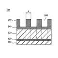
次に,ウエハWに対するプラズマ処理について図面を参照しながらより具体的に説明する。ここでは,例えば図2に示すような膜構造200を有するウエハWに対してエッチングを実行することで,図3に示すような被エッチング膜230にトレンチのパターンを形成する場合を例に挙げる。図2に示す膜構造200は,シリコン(Si)基材210上に酸化膜220,被エッチング膜230,反射防止膜240,レジストパターン250が積層して構成される。レジストパターン250にはトレンチを形成するための開口部260がパターニングされている。
(Wafer plasma treatment)
Next, the plasma processing for the wafer W will be described more specifically with reference to the drawings. Here, for example, a case where a trench pattern is formed in the
このようなウエハW上の被エッチング膜230をエッチングする場合には,先ず反射防止膜240をレジストパターン250をマスクとしてエッチングし,続いて被エッチング膜230をエッチングし,最後に残った反射防止膜240とレジストパターン250とを除去することにより,図3に示すようなトレンチを形成することができる。
When etching the
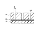
このとき,ウエハWの膜構造200に対してそのままエッチングを行うと,例えばレジストパターンの開口寸法が広がったり,被エッチング膜の凹部の側壁のエッチングが進みすぎてホールやトレンチの微小寸法(例えばホールの径やトレンチの線幅や溝幅)が目標値とずれてしまったりして,設計通りのデバイス特性が得られないという問題がある。図3は,トレンチの線幅d’が目標値dより小さくなってしまった例である。
At this time, if the
このため,本実施形態では,エッチングを行う前に,レジストパターン250に堆積物を堆積させる堆積ステップを行うことによってレジストパターン250の開口寸法を小さくしておき,その後にエッチングに移るようにする。この堆積ステップでは,例えば所定圧力にした処理室102内にCHF系ガスなどの処理ガスを供給してプラズマを発生させる。
For this reason, in the present embodiment, the opening size of the resist
ところで,このような堆積ステップにおいてレジストパターンに堆積物を良好に堆積させるためにはプリカーサであるラジカルの密度を高くすればよい。そのためには処理室102内の圧力を高くして処理ガスを供給することが望ましい。
By the way, in order to deposit deposits on the resist pattern in such a deposition step, the density of radicals as precursors may be increased. For that purpose, it is desirable to supply the processing gas by increasing the pressure in the
しかしながら,堆積ステップで処理室102内の圧力を高くするほど,エッチング後に形成されるトレンチの線幅又は溝幅の微小寸法(CD:Critical Dimension)にnmオーダー程度の僅かなばらつきが生じることがわかってきた。
However, it can be seen that as the pressure in the
そこで,発明者は様々な実験を行ってみたところ,処理ガスの流量を増大することで,ウエハ面内の堆積度合いのばらつきを大幅に抑制できることを見出した。これは,処理ガスの流量を増大することでウエハ径方向における処理ガスの解離度の差を抑制できるのでウエハ面内の堆積度合いのばらつきを抑制できると推察できる。 Therefore, the inventor conducted various experiments and found that by increasing the flow rate of the processing gas, variation in the degree of deposition within the wafer surface can be significantly suppressed. It can be inferred that, by increasing the flow rate of the processing gas, the difference in the degree of dissociation of the processing gas in the wafer radial direction can be suppressed, so that variations in the degree of deposition within the wafer surface can be suppressed.
すなわち,処理室102内の圧力が高いほど処理ガスの解離が進行しすぎてウエハの径方向の解離度に差が生じるため,ウエハ面内に堆積度合いのばらつきが生じやすい。これに対して,処理ガスの流量を増大することでウエハの径方向の解離度の差を抑制することでウエハ面内に生じる堆積度合いのばらつきを抑制できると考えられる。
That is, the higher the pressure in the
この点を処理ガスの流量と解離度との関係を用いてより具体的に説明する。一般にガス流量とガス解離度との関係は,横軸にガス流量の逆数をとり,縦軸に解離度の百分率をとると,図4に示すような曲線になる。図4において,黒丸はウエハ面内のセンタ部(中央部)での解離度であり,白四角はエッジ部(周縁部)の解離度である。 This point will be described more specifically using the relationship between the flow rate of the processing gas and the degree of dissociation. In general, the relationship between the gas flow rate and the gas dissociation degree is a curve as shown in FIG. 4 where the horizontal axis represents the reciprocal of the gas flow rate and the vertical axis represents the percentage of the dissociation degree. In FIG. 4, black circles indicate the degree of dissociation at the center (center) in the wafer surface, and white squares indicate the degree of dissociation at the edge (periphery).
図4に示す傾向を大局的に見れば,曲線の領域Bに示すように処理ガスの流量が少ないほどガス解離率も大きくなる傾向にある。ところが,その領域Bよりも処理ガスの流量をさらに増大すると,ガス解離率がほとんど変化しない領域Aがある。 If the tendency shown in FIG. 4 is seen broadly, the gas dissociation rate tends to increase as the flow rate of the processing gas decreases as shown in the region B of the curve. However, there is a region A in which the gas dissociation rate hardly changes when the flow rate of the processing gas is further increased than that of the region B.
ウエハWの面内位置(ここではセンタ部とエッジ部)によってはガスの解離の種類も若干変わるので図4に示す曲線上の位置も若干ずれることになる。このため,例えば従来のようにガス流量が200sccm程度の場合には領域Bになるので,この領域Bで堆積ステップを行うとウエハ面内のセンタ部(黒丸)とエッジ部(白四角)の解離度には差が生じる。 Depending on the in-plane position of the wafer W (here, the center portion and the edge portion), the type of gas dissociation slightly changes, so the position on the curve shown in FIG. For this reason, for example, when the gas flow rate is about 200 sccm as in the prior art, the region B is formed. Therefore, when the deposition step is performed in this region B, the center portion (black circle) and the edge portion (white square) in the wafer surface are dissociated. There is a difference in degrees.
これに対して,例えばガス流量を1000sccm以上に増大すると領域Aになるので,曲線上の位置がずれていても,ウエハ面内のセンタ部とエッジ部の解離度にはほとんど差が生じなくなる。このため,ガス流量を増大することで,ウエハ面内に堆積度合いのばらつきも抑制されると考えられる。なお,図4に示す領域Cでは,ガス解離率がほとんど変化しないものの,ガス流量が少なすぎて所望量の堆積物が堆積しないためこの領域は使えない。 On the other hand, for example, when the gas flow rate is increased to 1000 sccm or more, it becomes region A, so even if the position on the curve is shifted, there is almost no difference in the degree of dissociation between the center portion and the edge portion in the wafer surface. For this reason, it is considered that variation in the degree of deposition within the wafer surface can be suppressed by increasing the gas flow rate. In the region C shown in FIG. 4, although the gas dissociation rate hardly changes, this region cannot be used because the gas flow rate is too small to deposit a desired amount of deposits.
そこで,本実施形態では,処理ガスの流量を1000sccm以上に増大して堆積ステップを行った上でエッチングを行う。これによれば,ウエハ面内におけるレジストパターンの開口寸法のばらつきを抑制することができ,それによりエッチング後に形成されるトレンチの微小寸法(CD)のばらつきを抑制することができる。 Therefore, in this embodiment, the etching is performed after the deposition step is performed by increasing the flow rate of the processing gas to 1000 sccm or more. According to this, variation in the opening size of the resist pattern within the wafer surface can be suppressed, and thereby variation in the minute dimension (CD) of the trench formed after etching can be suppressed.
(ウエハ処理の具体例)
次に,このような本実施形態における堆積ステップを含むウエハ処理をプラズマ処理装置100により実行する場合の具体例について図面を参照しながら説明する。ここでは,図2に示すような膜構造200を有するウエハWに対して,先ず堆積ステップにてトレンチ形状の開口部260を有するレジストパターン250に堆積物270を堆積する堆積ステップを行った上でエッチングステップを行い,最後にアッシングステップを行うことによってトレンチを形成する。
(Specific example of wafer processing)
Next, a specific example in which the wafer processing including the deposition step in the present embodiment is executed by the
この場合の各ステップにおける膜構造の模式図を図5A〜図5Dに示す。図6は本実施形態の堆積ステップにおける処理の流れの概略を示す図である。なお,ここでのウエハ処理は,制御部160が所定のプログラムに基づいてプラズマ処理装置100の各部を制御することにより実行される。
Schematic diagrams of the film structure in each step in this case are shown in FIGS. 5A to 5D. FIG. 6 is a diagram showing an outline of the flow of processing in the deposition step of this embodiment. The wafer processing here is executed by the
(堆積ステップ)
先ず,処理室102内にウエハWを搬入して図6に示す堆積ステップを実行する。堆積ステップでは,ステップS110にて処理室102内を例えば100mTorr以上の高い圧力にする。次いでステップS120にて処理室102内に堆積ステップ用の処理ガス(例えばCHF3ガス)を1000sccm以上の大流量で供給し,下部電極110に第1高周波,第2高周波の各高周波電力を印加して処理ガスをプラズマ化する。こうして,堆積ステップが開始され,ウエハW上には例えばCとHとからなる堆積物が堆積し始める。
(Deposition step)
First, the wafer W is loaded into the
続いてステップS130にて堆積ステップの終了時間が経過したか否かを判断する。終了時間が経過したと判断した場合は,一連の堆積ステップを終了する。これにより,例えば図5Aに示すようにウエハW上に堆積物270が適切な膜厚で堆積する。堆積物270はレジストパターン250の上部とともに,開口部260の側壁に堆積する。これにより,レジストパターン250の開口部260を調整することによって,凹部の寸法D(又は図2に示す凸部の寸法d)を調整することができる。なお,堆積ステップの終了時間は,例えば記憶部164に処理レシピとして記憶されているものを読み出して用いることができる。
Subsequently, in step S130, it is determined whether or not the end time of the deposition step has elapsed. If it is determined that the end time has elapsed, the series of deposition steps is completed. Thereby, for example, as shown in FIG. 5A, the
(エッチングステップ)
次に,このように堆積物270が堆積した状態でエッチングステップを連続して行う。ここでのエッチングステップでは,先ず堆積物270をマスクとして反射防止膜240をエッチングし,その後に被エッチング膜230をエッチングする。反射防止膜240のエッチングでは,処理室102内の圧力を調整してエッチングガスとして例えばCHF3ガスとCF3lガスの混合ガスを供給し,下部電極110に第1高周波,第2高周波の各高周波電力を印加して処理ガスをプラズマ化する。このプラズマにより,反射防止膜240がエッチングされる。この反射防止膜240は,レジストパターン250と堆積物270と同様の有機系膜であるため,反射防止膜240のエッチングを行うと,レジストパターン250と堆積物270の露出部分もエッチングされて,例えば図5Bに示すように開口部260の底部に被エッチング膜230が露出する。
(Etching step)
Next, the etching step is continuously performed with the
なお,開口部260の底部に堆積物270が残留している場合には,それが無くなるまではCF3lガスの流量を減らすように流量比(CHF3ガス/CF3lガス)を制御して,堆積物のエッチングレートを低下させるようにしてもよい。これによれば開口部260の底部の堆積物が無くなるまで開口部260の側壁に堆積物を堆積させることができるので,より開口部260の径を小さくすることができる。
When the
続いて,被エッチング膜230のエッチングでは,被エッチング膜230が例えばSiN膜の場合には,エッチングガスとして例えばCHF3ガス,CF4ガス,及びArガスの混合ガスを供給し,下部電極110に第1高周波,第2高周波の各高周波電力を印加して処理ガスのプラズマを形成する。このプラズマにより,図5Cに示すように被エッチング膜230がエッチングされ,トレンチが形成される。
Subsequently, in the etching of the
なお,エッチングステップが終了すると,アッシングステップを行って,残りのレジストパターン250と反射防止膜240をすべて除去することにより,図5Dに示すように所望の溝幅微小寸法Dのトレンチが形成される。
When the etching step is completed, an ashing step is performed to remove all of the remaining resist
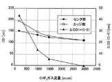
(ガス流量を変えた実験結果)
ここで,本実施形態にかかる堆積ステップをプラズマ処理装置100を用いて行った実験結果を図面を参照しながら説明する。ここでは,処理室102内の圧力を150mTorrに固定して,CHF3ガスを処理ガスとしてその流量を変えてそれぞれ堆積ステップを行った。CHF3ガスを1000sccm以上の大流量(ここでは1000sccm,1500sccm,3000sccm)供給した場合を200sccmの小流量供給した場合と比較する。
(Experimental results with different gas flow rates)
Here, an experimental result of performing the deposition step according to the present embodiment using the
図7はそれぞれの堆積ステップ後にウエハWの高さ方向のデポジションレートを測定してプロットしたものである。図7では,横軸にウエハ面内位置をとり,縦軸にデポジションレートをとっている。なお,その他の堆積ステップの処理条件は以下の通りである。 FIG. 7 shows the measured deposition rate in the height direction of the wafer W after each deposition step. In FIG. 7, the horizontal axis represents the position in the wafer plane, and the vertical axis represents the deposition rate. The processing conditions for the other deposition steps are as follows.
[堆積ステップの処理条件]
第1高周波電力:750W
第2高周波電力:300W
上部電極温度:60deg
側壁温度:60deg
下部電極温度:40deg
処理時間:60sec
[Processing conditions for deposition step]
First high frequency power: 750 W
Second high frequency power: 300W
Upper electrode temperature: 60 deg
Side wall temperature: 60deg
Lower electrode temperature: 40 deg
Processing time: 60 sec
図7によれば,CHF3ガスを1000sccm以上の大流量供給した場合は,200sccmの小流量供給した場合に比してデポジションレートの面内均一性が大幅に向上していることがわかる。 According to FIG. 7, it can be seen that when the CHF 3 gas is supplied at a large flow rate of 1000 sccm or more, the in-plane uniformity of the deposition rate is greatly improved as compared with the case where a low flow rate of 200 sccm is supplied.
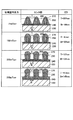
また,200sccm,1000sccm,1500sccm,3000sccmの各実験においてウエハWのセンタ部とエッジ部における開口部を比較したものをそれぞれ図8A〜図8Dに示す。図8A〜図8Dにおいて,センタ部の開口底部の溝幅微小寸法(溝幅CD)をC,エッジ部の開口底部の溝幅微小寸法(溝幅CD)をEとし,その寸法差をΔCD(=C−E)とすると,ΔCDは,200sccmの場合には18nmであるのに対して,1000sccm,1500sccm,3000sccmと流量を増大していくほど,6nm,4nm,0nmと大幅に減少していることがわかる。 8A to 8D show the comparison of the opening at the center portion and the edge portion of the wafer W in each experiment of 200 sccm, 1000 sccm, 1500 sccm, and 3000 sccm. 8A to 8D, C is the groove width minute dimension (groove width CD) at the opening bottom of the center part, E is the groove width minute dimension (groove width CD) of the opening bottom part of the edge part, and ΔD ( = C−E), ΔCD is 18 nm in the case of 200 sccm, but greatly decreases to 6 nm, 4 nm, and 0 nm as the flow rate is increased to 1000 sccm, 1500 sccm, and 3000 sccm. I understand that.
さらに,上記と同様の実験をレジストパターンを変えて行った場合の実験結果を図9A〜図9Dに示す。図9A,図9B,図9Cは密のレジストパターンの場合であり,図9Dは粗のレジストパターンの場合である。さらに図9A,図9B,図9Cはそれぞれ,線幅と溝幅の割合が1:1,1:2,1:3の場合である。図9A〜図9Dはそれぞれのレジストパターンが形成されたウエハに対して上記と同様の実験を行って,横軸にCHF3ガスの流量をとり,縦軸にセンタ部とエッジ部の溝幅CDとこれらの寸法差ΔCDをとってグラフにしたものである。 Furthermore, FIG. 9A to FIG. 9D show experimental results when the same experiment as described above is performed with the resist pattern changed. 9A, 9B, and 9C are cases of a dense resist pattern, and FIG. 9D is a case of a coarse resist pattern. Further, FIG. 9A, FIG. 9B, and FIG. 9C are cases where the ratio of the line width and the groove width is 1: 1, 1: 2, and 1: 3, respectively. 9A to 9D, the same experiment as described above was performed on the wafer on which each resist pattern was formed, the flow rate of CHF 3 gas was taken on the horizontal axis, and the groove width CD of the center portion and the edge portion on the vertical axis. These dimensional differences ΔCD are graphed.
図9A〜図9Dによれば,すべての場合においてCHF3ガスを1000sccm以上の大流量供給した場合は,200sccmの小流量供給した場合に比してセンタ部とエッジ部の寸法差ΔCDが大幅に減少している。さらに,CHF3ガスを1000sccm以上供給した場合は,3000sccmまでの範囲では流量が大きくなるほどセンタ部とエッジ部の寸法差ΔCDが減少する。しかも,寸法差ΔCDの減少する変化率はレジストパターンが密から粗になるに連れて大きくなる。 According to FIGS. 9A to 9D, in all cases, when the CHF 3 gas is supplied at a large flow rate of 1000 sccm or more, the dimensional difference ΔCD between the center portion and the edge portion is significantly larger than when the low flow rate of 200 sccm is supplied. is decreasing. Further, when CHF 3 gas is supplied at 1000 sccm or more, the dimensional difference ΔCD between the center portion and the edge portion decreases as the flow rate increases up to 3000 sccm. Moreover, the rate of change of the dimensional difference ΔCD increases as the resist pattern becomes denser and rougher.
このように,本実施形態では,堆積ステップにおいて処理室102内の圧力を例えば100mTorr以上の高い圧力にすることでラジカル密度を高めつつ,処理ガスを1000sccm以上の大流量で供給することでウエハ面内における堆積物270の堆積量のばらつきを抑えることができる。これにより,エッチング後に形成されるトレンチの微小寸法(CD)変化量のばらつきを抑えることができるので,ウエハ面内の全域にわたって設計通りのトレンチを形成できる。
As described above, in this embodiment, in the deposition step, the processing surface is supplied at a high flow rate of 1000 sccm or higher while the radical density is increased by setting the pressure in the
上記実験結果に鑑みれば,処理ガスがCHF3ガスの場合にはその流量が3000sccmまでの範囲では1000sccm以上にすることが好ましく,1500sccm以上にすることがより好ましい。 In view of the above experimental results, when the processing gas is CHF 3 gas, the flow rate is preferably 1000 sccm or more, more preferably 1500 sccm or more in the range up to 3000 sccm.
また,上記実験では処理室102内の圧力を150mTorrに固定したが,これに限られるものではなく150mTorrより高い圧力に設定してもよい。なお,処理室102内の圧力が高い方が開口部の側壁に満遍なく堆積物を堆積させることができる。
In the above experiment, the pressure in the
(処理室内圧力を変えた実験結果)
ここで,CHF3ガスの流量を固定して処理室102内の圧力を変えてそれぞれ堆積ステップを行った実験結果について図面を参照しながら説明する。ここでは,CHF3ガスの流量を少量の100sccmに固定して,処理室102内の圧力を150mTorr以上(ここでは,150mTorr,200mTorr,250mTorr)の場合を,75mTorrにした場合と比較する。
(Experimental result of changing the processing chamber pressure)
Here, the results of experiments in which the deposition step is performed by changing the pressure in the
図10はそれぞれの堆積ステップ後に開口部のトップ部とボトム部の溝幅CDを測定して比較したものである。図11はこれらの溝幅CDを縦軸にとって,横軸に処理室内圧力をとってグラフにしたものである。なお,その他の堆積ステップの処理条件は上述したものと同様である。 FIG. 10 compares the groove width CD of the top and bottom of the opening after each deposition step. FIG. 11 is a graph in which the groove width CD is taken as the vertical axis and the processing chamber pressure is taken along the horizontal axis. The processing conditions of the other deposition steps are the same as those described above.
図10,図11によれば,処理室102内の圧力が75mTorrのように低い場合には,開口部の側壁にトップ部からボトム部にかけて溝幅が小さくなるように傾斜して堆積物が堆積する。
According to FIGS. 10 and 11, when the pressure in the
これに対して,150mTorr以上の高い圧力の場合には,開口部の側壁にトップ部からボトム部にかけて溝幅がほぼ変わらず,ほぼ垂直に堆積物が堆積する。しかも,250mTorrまでの範囲では処理室102内の圧力が高くなるほど,トップ部とボトム部との寸法差が小さくなることがわかる。
On the other hand, in the case of a high pressure of 150 mTorr or more, the groove width is almost unchanged from the top portion to the bottom portion on the side wall of the opening, and deposits are deposited almost vertically. In addition, it can be seen that in the range up to 250 mTorr, the dimensional difference between the top portion and the bottom portion decreases as the pressure in the
このように図10,図11に示す実験結果によれば,開口部のトップ部からボトム部の寸法差を少なくするには,処理室102内の圧力は150mTorr以上がより好ましい。なお,図10,図11に示す実験のようにCHF3ガスが100sccm程度の少量の場合には,150mTorr以上では処理室102内の圧力を高くするほど開口部の底部への堆積量が増加する。
As described above, according to the experimental results shown in FIGS. 10 and 11, the pressure in the
この点,CHF3ガスの流量を1000sccm以上に増大させると,図8B〜図8Dに示すように,開口部の側壁に垂直に堆積物を堆積させることができるとともに,開口部の底部に堆積物が堆積することを抑制できる。 In this regard, when the flow rate of the CHF 3 gas is increased to 1000 sccm or more, as shown in FIGS. 8B to 8D, deposits can be deposited perpendicularly to the side walls of the openings, and deposits can be deposited at the bottom of the openings. Can be prevented from being deposited.
なお,本実施形態ではウエハW上にトレンチのパターンを形成した場合について説明したが,トレンチの代わりに,ホールを形成する場合に本発明を適用してもよい。また,上記実施形態にかかる堆積ステップでは,被エッチング膜上にレジストパターンを形成したウエハを用いた場合を例に挙げて説明したが,必ずしもこれに限定されるものではない。例えば被エッチング膜とレジストパターンとの間に有機膜からなる下層レジスト膜を形成したウエハを用いてもよい。具体的には図12に示すように被エッチング膜230の上に下層レジスト膜252,そのマスク254を形成した上に反射防止膜240,レジストパターン250を形成したウエハを用いてそのレジストパターン250に堆積物を堆積させてもよい。
In the present embodiment, the case where the trench pattern is formed on the wafer W has been described. However, the present invention may be applied to the case where a hole is formed instead of the trench. Moreover, although the case where the wafer which formed the resist pattern on the to-be-etched film was mentioned as an example and demonstrated in the deposition step concerning the said embodiment, it is not necessarily limited to this. For example, a wafer in which a lower resist film made of an organic film is formed between the film to be etched and the resist pattern may be used. Specifically, as shown in FIG. 12, the resist
また,本実施形態では被エッチング膜がSiN膜の場合を例に挙げて説明したが,これに限られるものではない。例えばレジストパターン250をマスクとしてエッチングする薄膜であればどのような被エッチング膜230に適用してもよい。被エッチング膜230としては例えばSiO2などの酸化膜,SiNなどの窒化膜,Si膜の他,TEOS膜,Ti膜,TiN膜などのメタル膜が挙げられる。
In this embodiment, the case where the film to be etched is a SiN film has been described as an example. However, the present invention is not limited to this. For example, any
また,堆積ステップにおいて処理ガスのレジデンスタイムは,開口部の底部よりも側壁に堆積物を堆積させ易くする観点から,例えば0.1秒以下にすることが好ましい。 Further, in the deposition step, the residence time of the processing gas is preferably set to 0.1 seconds or less, for example, from the viewpoint of facilitating deposition of deposits on the side wall rather than the bottom of the opening.
ここで,レジデンスタイムとは,処理ガスの処理室102内の処理に寄与する部分における滞留時間を意味し,下部電極面積(図1では,ウエハWの面積とフォーカスリング15の面積の合計)に上下の電極間距離を乗算して求めた処理室内の有効体積,すなわち処理ガスがプラズマ化する空間の体積をV[m3],排気速度をS[m3/秒],処理室102内の圧力をp[Pa],処理ガスの総流量をQ(Pa・m3/秒)とすれば,レジデンスタイムτ[秒]は,下記(1)式に基づいて求めることができる。
Here, the residence time means the residence time of the portion of the processing gas that contributes to the processing in the
τ=V/S=pV/Q ・・・(1) τ = V / S = pV / Q (1)
また,上述した実施形態の機能を実現するソフトウエアのプログラムを記憶した記憶媒体等の媒体をシステムあるいは装置に供給し,そのシステムあるいは装置のコンピュータ(又はCPUやMPU)が記憶媒体等の媒体に記憶されたプログラムを読み出して実行することによっても,本発明が達成され得る。 In addition, a medium such as a storage medium storing a software program for realizing the functions of the above-described embodiments is supplied to the system or apparatus, and the computer (or CPU or MPU) of the system or apparatus stores the medium in the storage medium or the like. The present invention can also be achieved by reading and executing a stored program.
この場合,記憶媒体等の媒体から読み出されたプログラム自体が上述した実施形態の機能を実現することになり,そのプログラムを記憶した記憶媒体等の媒体は本発明を構成することになる。プログラムを供給するための記憶媒体等の媒体としては,例えば,フロッピー(登録商標)ディスク,ハードディスク,光ディスク,光磁気ディスク,CD−ROM,CD−R,CD−RW,DVD−ROM,DVD−RAM,DVD−RW,DVD+RW,磁気テープ,不揮発性のメモリカード,ROMなどが挙げられる。また,媒体に対してプログラムを,ネットワークを介してダウンロードして提供することも可能である。 In this case, the program itself read from the medium such as a storage medium realizes the functions of the above-described embodiment, and the medium such as the storage medium storing the program constitutes the present invention. Examples of the medium such as a storage medium for supplying the program include a floppy (registered trademark) disk, a hard disk, an optical disk, a magneto-optical disk, a CD-ROM, a CD-R, a CD-RW, a DVD-ROM, and a DVD-RAM. DVD-RW, DVD + RW, magnetic tape, nonvolatile memory card, ROM, and the like. It is also possible to provide a program downloaded to a medium via a network.
なお,コンピュータが読み出したプログラムを実行することにより,上述した実施形態の機能が実現されるだけでなく,そのプログラムの指示に基づき,コンピュータ上で稼動しているOSなどが実際の処理の一部又は全部を行い,その処理によって上述した実施形態の機能が実現される場合も,本発明に含まれる。 Note that by executing the program read by the computer, not only the functions of the above-described embodiments are realized, but also an OS or the like running on the computer is part of the actual processing based on the instructions of the program. Alternatively, the case where the functions of the above-described embodiment are realized by performing all of the above processing is also included in the present invention.
さらに,記憶媒体等の媒体から読み出されたプログラムが,コンピュータに挿入された機能拡張ボードやコンピュータに接続された機能拡張ユニットに備わるメモリに書き込まれた後,そのプログラムの指示に基づき,その機能拡張ボードや機能拡張ユニットに備わるCPUなどが実際の処理の一部又は全部を行い,その処理によって上述した実施形態の機能が実現される場合も,本発明に含まれる。 Furthermore, after a program read from a medium such as a storage medium is written to a memory provided in a function expansion board inserted into the computer or a function expansion unit connected to the computer, the function is determined based on the instructions of the program. The present invention also includes the case where the CPU or the like provided in the expansion board or the function expansion unit performs part or all of the actual processing and the functions of the above-described embodiments are realized by the processing.
以上,添付図面を参照しながら本発明の好適な実施形態について説明したが,本発明は係る例に限定されないことは言うまでもない。当業者であれば,特許請求の範囲に記載された範疇内において,各種の変更例または修正例に想到し得ることは明らかであり,それらについても当然に本発明の技術的範囲に属するものと了解される。 As mentioned above, although preferred embodiment of this invention was described referring an accompanying drawing, it cannot be overemphasized that this invention is not limited to the example which concerns. It will be apparent to those skilled in the art that various changes and modifications can be made within the scope of the claims, and these are naturally within the technical scope of the present invention. Understood.
例えば上記実施形態では基板処理装置として,下部電極のみに2種類の高周波電力を重畳して印加してプラズマを生起させるタイプのプラズマ処理装置を例に挙げて説明したが,これに限定されるものではなく,別のタイプ例えば下部電極のみに1種類の高周波電力を印加するタイプや2種類の高周波電力を上部電極と下部電極にそれぞれ印加するタイプのプラズマ処理装置に適用してもよい。さらに,本発明を適用可能な基板処理装置としては,プラズマ処理装置に限定されることはなく,成膜処理を行う熱処理装置に適用してもよい。 For example, in the above embodiment, as the substrate processing apparatus, a plasma processing apparatus of a type that generates plasma by superimposing and applying two types of high-frequency power to only the lower electrode has been described, but the present invention is not limited thereto. Instead, the plasma processing apparatus may be applied to another type, for example, a type in which only one type of high-frequency power is applied only to the lower electrode or a type in which two types of high-frequency power are applied to the upper electrode and the lower electrode, respectively. Furthermore, the substrate processing apparatus to which the present invention can be applied is not limited to the plasma processing apparatus, and may be applied to a heat treatment apparatus that performs a film forming process.
本発明は,例えば半導体ウエハ,FPD基板などの基板上に薄膜を堆積させる堆積ステップを行う基板処理方法,基板処理装置,記憶媒体に適用可能である。 The present invention can be applied to a substrate processing method, a substrate processing apparatus, and a storage medium that perform a deposition step of depositing a thin film on a substrate such as a semiconductor wafer or an FPD substrate.
100 プラズマ処理装置
102 処理室
104 筒状部
106 筒状保持部
108 ゲートバルブ
110 下部電極
112 静電チャック
114 静電チャック電極
115 直流電源
116 冷媒室
118 伝熱ガス供給ライン
119 フォーカスリング
120 上部電極
122 処理ガス供給部
123 配管
124 電極板
125 ガス通気孔
126 電極支持体
127 バッファ室
128 ガス導入口
130 排気路
132 バッフル板
134 排気口
136 排気部
140 電力供給装置
142 第1高周波電力供給機構
144 第1フィルタ
146 第1整合器
148 第1電源
152 第2高周波電力供給機構
154 第2フィルタ
156 第2整合器
158 第2電源
160 制御部
162 操作部
164 記憶部
170 磁場形成部
172 上部マグネットリング
174 下部マグネットリング
200 膜構造
210 シリコン基材
220 酸化膜
230 被エッチング膜
240 反射防止膜
250 レジストパターン
252 下層レジスト膜
254 マスク
260 開口部
270 堆積物
W ウエハ
DESCRIPTION OF
Claims (13)
被エッチング膜上に形成された反射防止膜上に,複数の開口部を有するレジストパターンが形成された前記基板に対して,前記被エッチング膜をエッチングする前に前記レジストパターンの各開口部の側壁に堆積物を堆積させるステップを有し,
前記堆積ステップ後に前記エッチングを連続して行い,
前記堆積ステップは,前記処理室内の圧力を100mTorr以上にし,CHF系ガスを1000sccm以上導入してプラズマを生起することを特徴とする基板処理方法。 The chamber is placed on the lower electrode by generating a plasma of a predetermined gas by applying a high-frequency power between the electrodes in a processing chamber configured to be able to be depressurized and arranged with the upper electrode and the lower electrode facing each other. A substrate processing method for performing predetermined processing on a substrate,
Side walls of the openings of the resist pattern before etching the etched film on the substrate on which the resist pattern having a plurality of openings is formed on the antireflection film formed on the etched film. Depositing deposits on the
Performing the etching continuously after the deposition step;
In the deposition step, plasma is generated by setting the pressure in the processing chamber to 100 mTorr or more and introducing a CHF-based gas at 1000 sccm or more.
前記下部電極に所定の高周波電力を印加する電力供給装置と,
前記処理室内に所定のガスを供給するガス供給部と,
前記処理室内を排気して所定の圧力に減圧する排気部と,
被エッチング膜上に形成された反射防止膜上に,複数の開口部を有するレジストパターンが形成された前記基板に対して,前記被エッチング膜をエッチングする前に前記レジストパターンの各開口部の側壁に堆積物を堆積させるステップを実行する制御部を,備え,
前記制御部は,前記堆積ステップ後に前記エッチングを連続して行い,前記堆積ステップにおいて前記処理室内の圧力を100mTorr以上にし,CHF系ガスを1000sccm以上導入してプラズマを生起することを特徴とすることを特徴とする基板処理装置。 The chamber is placed on the lower electrode by generating a plasma of a predetermined gas by applying a high-frequency power between the electrodes in a processing chamber configured to be able to be depressurized and arranged with the upper electrode and the lower electrode facing each other. A substrate processing apparatus for performing predetermined processing on a substrate,
A power supply device for applying a predetermined high-frequency power to the lower electrode;
A gas supply unit for supplying a predetermined gas into the processing chamber;
An exhaust section for exhausting the processing chamber and reducing the pressure to a predetermined pressure;
Side walls of the openings of the resist pattern before etching the etched film on the substrate on which the resist pattern having a plurality of openings is formed on the antireflection film formed on the etched film. A controller for performing the step of depositing the deposit on
The control unit continuously performs the etching after the deposition step, and in the deposition step, a pressure in the processing chamber is set to 100 mTorr or more, and a CHF-based gas is introduced to 1000 sccm or more to generate plasma. A substrate processing apparatus.
A computer-readable recording medium in which a program for executing the deposition step according to claim 1 is recorded.
Priority Applications (2)
| Application Number | Priority Date | Filing Date | Title |
|---|---|---|---|
| JP2009261018A JP5357710B2 (en) | 2009-11-16 | 2009-11-16 | Substrate processing method, substrate processing apparatus, and recording medium recording program |
| US12/943,967 US8524331B2 (en) | 2009-11-16 | 2010-11-11 | Substrate processing method |
Applications Claiming Priority (1)
| Application Number | Priority Date | Filing Date | Title |
|---|---|---|---|
| JP2009261018A JP5357710B2 (en) | 2009-11-16 | 2009-11-16 | Substrate processing method, substrate processing apparatus, and recording medium recording program |
Publications (3)
| Publication Number | Publication Date |
|---|---|
| JP2011108782A JP2011108782A (en) | 2011-06-02 |
| JP2011108782A5 JP2011108782A5 (en) | 2012-12-27 |
| JP5357710B2 true JP5357710B2 (en) | 2013-12-04 |
Family
ID=44011469
Family Applications (1)
| Application Number | Title | Priority Date | Filing Date |
|---|---|---|---|
| JP2009261018A Expired - Fee Related JP5357710B2 (en) | 2009-11-16 | 2009-11-16 | Substrate processing method, substrate processing apparatus, and recording medium recording program |
Country Status (2)
| Country | Link |
|---|---|
| US (1) | US8524331B2 (en) |
| JP (1) | JP5357710B2 (en) |
Families Citing this family (20)
| Publication number | Priority date | Publication date | Assignee | Title |
|---|---|---|---|---|
| EP2251671B1 (en) | 2009-05-13 | 2017-04-26 | SiO2 Medical Products, Inc. | Outgassing method for inspecting a coated surface |
| US9458536B2 (en) | 2009-07-02 | 2016-10-04 | Sio2 Medical Products, Inc. | PECVD coating methods for capped syringes, cartridges and other articles |
| US11624115B2 (en) | 2010-05-12 | 2023-04-11 | Sio2 Medical Products, Inc. | Syringe with PECVD lubrication |
| US9878101B2 (en) | 2010-11-12 | 2018-01-30 | Sio2 Medical Products, Inc. | Cyclic olefin polymer vessels and vessel coating methods |
| US9272095B2 (en) | 2011-04-01 | 2016-03-01 | Sio2 Medical Products, Inc. | Vessels, contact surfaces, and coating and inspection apparatus and methods |
| KR20130004830A (en) * | 2011-07-04 | 2013-01-14 | 삼성디스플레이 주식회사 | Apparatus for thin layer deposition and method for manufacturing of organic light emitting display apparatus using the same |
| US11116695B2 (en) | 2011-11-11 | 2021-09-14 | Sio2 Medical Products, Inc. | Blood sample collection tube |
| CN103930595A (en) | 2011-11-11 | 2014-07-16 | Sio2医药产品公司 | Passivation, ph protective or lubricity coating for pharmaceutical package, coating process and apparatus |
| CA2887352A1 (en) | 2012-05-09 | 2013-11-14 | Sio2 Medical Products, Inc. | Saccharide protective coating for pharmaceutical package |
| CN104854257B (en) | 2012-11-01 | 2018-04-13 | Sio2医药产品公司 | coating inspection method |
| WO2014078666A1 (en) | 2012-11-16 | 2014-05-22 | Sio2 Medical Products, Inc. | Method and apparatus for detecting rapid barrier coating integrity characteristics |
| CN103832965B (en) * | 2012-11-23 | 2017-02-08 | 北京北方微电子基地设备工艺研究中心有限责任公司 | Substrate etching method |
| EP2925903B1 (en) | 2012-11-30 | 2022-04-13 | Si02 Medical Products, Inc. | Controlling the uniformity of pecvd deposition on medical syringes, cartridges, and the like |
| US9764093B2 (en) | 2012-11-30 | 2017-09-19 | Sio2 Medical Products, Inc. | Controlling the uniformity of PECVD deposition |
| EP2961858B1 (en) | 2013-03-01 | 2022-09-07 | Si02 Medical Products, Inc. | Coated syringe. |
| US9937099B2 (en) | 2013-03-11 | 2018-04-10 | Sio2 Medical Products, Inc. | Trilayer coated pharmaceutical packaging with low oxygen transmission rate |
| KR102167557B1 (en) | 2013-03-11 | 2020-10-20 | 에스아이오2 메디컬 프로덕츠, 인크. | Coated Packaging |
| US20160017490A1 (en) | 2013-03-15 | 2016-01-21 | Sio2 Medical Products, Inc. | Coating method |
| US11066745B2 (en) | 2014-03-28 | 2021-07-20 | Sio2 Medical Products, Inc. | Antistatic coatings for plastic vessels |
| CA3204930A1 (en) | 2015-08-18 | 2017-02-23 | Sio2 Medical Products, Inc. | Pharmaceutical and other packaging with low oxygen transmission rate |
Family Cites Families (18)
| Publication number | Priority date | Publication date | Assignee | Title |
|---|---|---|---|---|
| US5290383A (en) * | 1991-03-24 | 1994-03-01 | Tokyo Electron Limited | Plasma-process system with improved end-point detecting scheme |
| JP2001267310A (en) * | 2000-03-17 | 2001-09-28 | Tokyo Electron Ltd | Method and device for film forming plasma |
| KR100361585B1 (en) * | 2000-11-11 | 2002-11-22 | 한국과학기술연구원 | Preparation of Hexafluoropropylene(HFP) by the pyrolysis of trifluoromethane(R23) and tetrafluoroethylene(TFE) |
| US7169695B2 (en) | 2002-10-11 | 2007-01-30 | Lam Research Corporation | Method for forming a dual damascene structure |
| JP2004152977A (en) * | 2002-10-30 | 2004-05-27 | Renesas Technology Corp | Semiconductor storage device |
| JP2004311706A (en) * | 2003-04-07 | 2004-11-04 | Toshiba Corp | Semiconductor device and its manufacturing method |
| JP4422624B2 (en) * | 2004-03-03 | 2010-02-24 | 日本航空電子工業株式会社 | Micro movable device and manufacturing method thereof |
| JP2006156591A (en) * | 2004-11-26 | 2006-06-15 | Matsushita Electric Ind Co Ltd | Method for manufacturing semiconductor device |
| US7271107B2 (en) * | 2005-02-03 | 2007-09-18 | Lam Research Corporation | Reduction of feature critical dimensions using multiple masks |
| JP2007194284A (en) * | 2006-01-17 | 2007-08-02 | Tokyo Electron Ltd | Plasma treatment method, plasma treatment device, and storage medium |
| JP4946138B2 (en) * | 2006-03-31 | 2012-06-06 | 東京エレクトロン株式会社 | Etching method |
| US7309646B1 (en) * | 2006-10-10 | 2007-12-18 | Lam Research Corporation | De-fluoridation process |
| JP5161503B2 (en) * | 2007-07-09 | 2013-03-13 | ルネサスエレクトロニクス株式会社 | Manufacturing method of semiconductor device |
| JP5276926B2 (en) * | 2008-08-25 | 2013-08-28 | ラピスセミコンダクタ株式会社 | Contact hole side wall resistance measurement method |
| JP5128421B2 (en) * | 2008-09-04 | 2013-01-23 | 東京エレクトロン株式会社 | Plasma processing method and resist pattern modification method |
| JP5191857B2 (en) * | 2008-10-08 | 2013-05-08 | 東京エレクトロン株式会社 | Substrate processing method, substrate processing apparatus, storage medium |
| JP5180121B2 (en) * | 2009-02-20 | 2013-04-10 | 東京エレクトロン株式会社 | Substrate processing method |
| US8197915B2 (en) * | 2009-04-01 | 2012-06-12 | Asm Japan K.K. | Method of depositing silicon oxide film by plasma enhanced atomic layer deposition at low temperature |
-
2009
- 2009-11-16 JP JP2009261018A patent/JP5357710B2/en not_active Expired - Fee Related
-
2010
- 2010-11-11 US US12/943,967 patent/US8524331B2/en not_active Expired - Fee Related
Also Published As
| Publication number | Publication date |
|---|---|
| US20110117288A1 (en) | 2011-05-19 |
| JP2011108782A (en) | 2011-06-02 |
| US8524331B2 (en) | 2013-09-03 |
Similar Documents
| Publication | Publication Date | Title |
|---|---|---|
| JP5357710B2 (en) | Substrate processing method, substrate processing apparatus, and recording medium recording program | |
| JP5530088B2 (en) | Plasma etching method and plasma etching apparatus | |
| US9324569B2 (en) | Plasma etching method and plasma etching apparatus | |
| TWI525694B (en) | Chamber cleaning method | |
| US8679358B2 (en) | Plasma etching method and computer-readable storage medium | |
| JP5642001B2 (en) | Plasma etching method | |
| JP5442403B2 (en) | Substrate processing apparatus, cleaning method therefor, and recording medium recording program | |
| JP2008078515A (en) | Plasma treatment method | |
| KR101858324B1 (en) | Plasma etching method | |
| US20130029493A1 (en) | Plasma etching method, control program and computer storage medium | |
| KR101068014B1 (en) | Plasma etching method, plasma etching apparatus and computer-readable storage medium | |
| US20200035503A1 (en) | Plasma processing method and plasma processing apparatus | |
| US10651077B2 (en) | Etching method | |
| TWI540633B (en) | Surface planarization method | |
| US11557485B2 (en) | Plasma processing method and plasma processing apparatus | |
| US7655572B2 (en) | Semiconductor device manufacturing method, semiconductor device manufacturing apparatus, control program and computer storage medium | |
| JP2019145540A (en) | Cleaning method and plasma processing apparatus | |
| JP5804978B2 (en) | Plasma etching method and computer recording medium | |
| US20240006168A1 (en) | Substrate processing method, component processing method, and substrate processing apparatus | |
| US20070218691A1 (en) | Plasma etching method, plasma etching apparatus and computer-readable storage medium | |
| JP2007251044A (en) | Plasma etching method, plasma etching equipment and computer storage medium | |
| JP2015201583A (en) | Plasma etching method and apparatus | |
| JP2015106587A (en) | Method for coating electrostatic chuck and plasma processing apparatus |
Legal Events
| Date | Code | Title | Description |
|---|---|---|---|
| A521 | Request for written amendment filed |
Free format text: JAPANESE INTERMEDIATE CODE: A523 Effective date: 20121114 |
|
| A621 | Written request for application examination |
Free format text: JAPANESE INTERMEDIATE CODE: A621 Effective date: 20121114 |
|
| A977 | Report on retrieval |
Free format text: JAPANESE INTERMEDIATE CODE: A971007 Effective date: 20130709 |
|
| A131 | Notification of reasons for refusal |
Free format text: JAPANESE INTERMEDIATE CODE: A131 Effective date: 20130716 |
|
| A521 | Request for written amendment filed |
Free format text: JAPANESE INTERMEDIATE CODE: A523 Effective date: 20130807 |
|
| TRDD | Decision of grant or rejection written | ||
| A01 | Written decision to grant a patent or to grant a registration (utility model) |
Free format text: JAPANESE INTERMEDIATE CODE: A01 Effective date: 20130822 |
|
| A61 | First payment of annual fees (during grant procedure) |
Free format text: JAPANESE INTERMEDIATE CODE: A61 Effective date: 20130830 |
|
| R150 | Certificate of patent or registration of utility model |
Ref document number: 5357710 Country of ref document: JP Free format text: JAPANESE INTERMEDIATE CODE: R150 Free format text: JAPANESE INTERMEDIATE CODE: R150 |
|
| R250 | Receipt of annual fees |
Free format text: JAPANESE INTERMEDIATE CODE: R250 |
|
| LAPS | Cancellation because of no payment of annual fees |