EP2077602A1 - Wireless ic device - Google Patents
Wireless ic device Download PDFInfo
- Publication number
- EP2077602A1 EP2077602A1 EP08790581A EP08790581A EP2077602A1 EP 2077602 A1 EP2077602 A1 EP 2077602A1 EP 08790581 A EP08790581 A EP 08790581A EP 08790581 A EP08790581 A EP 08790581A EP 2077602 A1 EP2077602 A1 EP 2077602A1
- Authority
- EP
- European Patent Office
- Prior art keywords
- coupler
- wireless
- feeder circuit
- mount
- chip
- Prior art date
- Legal status (The legal status is an assumption and is not a legal conclusion. Google has not performed a legal analysis and makes no representation as to the accuracy of the status listed.)
- Granted
Links
Images




Classifications
-
- H—ELECTRICITY
- H01—ELECTRIC ELEMENTS
- H01Q—ANTENNAS, i.e. RADIO AERIALS
- H01Q9/00—Electrically-short antennas having dimensions not more than twice the operating wavelength and consisting of conductive active radiating elements
- H01Q9/04—Resonant antennas
- H01Q9/16—Resonant antennas with feed intermediate between the extremities of the antenna, e.g. centre-fed dipole
-
- G—PHYSICS
- G06—COMPUTING OR CALCULATING; COUNTING
- G06K—GRAPHICAL DATA READING; PRESENTATION OF DATA; RECORD CARRIERS; HANDLING RECORD CARRIERS
- G06K19/00—Record carriers for use with machines and with at least a part designed to carry digital markings
- G06K19/06—Record carriers for use with machines and with at least a part designed to carry digital markings characterised by the kind of the digital marking, e.g. shape, nature, code
- G06K19/067—Record carriers with conductive marks, printed circuits or semiconductor circuit elements, e.g. credit or identity cards also with resonating or responding marks without active components
- G06K19/07—Record carriers with conductive marks, printed circuits or semiconductor circuit elements, e.g. credit or identity cards also with resonating or responding marks without active components with integrated circuit chips
- G06K19/077—Constructional details, e.g. mounting of circuits in the carrier
- G06K19/07749—Constructional details, e.g. mounting of circuits in the carrier the record carrier being capable of non-contact communication, e.g. constructional details of the antenna of a non-contact smart card
-
- G—PHYSICS
- G06—COMPUTING OR CALCULATING; COUNTING
- G06K—GRAPHICAL DATA READING; PRESENTATION OF DATA; RECORD CARRIERS; HANDLING RECORD CARRIERS
- G06K19/00—Record carriers for use with machines and with at least a part designed to carry digital markings
- G06K19/06—Record carriers for use with machines and with at least a part designed to carry digital markings characterised by the kind of the digital marking, e.g. shape, nature, code
- G06K19/067—Record carriers with conductive marks, printed circuits or semiconductor circuit elements, e.g. credit or identity cards also with resonating or responding marks without active components
- G06K19/07—Record carriers with conductive marks, printed circuits or semiconductor circuit elements, e.g. credit or identity cards also with resonating or responding marks without active components with integrated circuit chips
- G06K19/077—Constructional details, e.g. mounting of circuits in the carrier
-
- G—PHYSICS
- G06—COMPUTING OR CALCULATING; COUNTING
- G06K—GRAPHICAL DATA READING; PRESENTATION OF DATA; RECORD CARRIERS; HANDLING RECORD CARRIERS
- G06K19/00—Record carriers for use with machines and with at least a part designed to carry digital markings
- G06K19/06—Record carriers for use with machines and with at least a part designed to carry digital markings characterised by the kind of the digital marking, e.g. shape, nature, code
- G06K19/067—Record carriers with conductive marks, printed circuits or semiconductor circuit elements, e.g. credit or identity cards also with resonating or responding marks without active components
- G06K19/07—Record carriers with conductive marks, printed circuits or semiconductor circuit elements, e.g. credit or identity cards also with resonating or responding marks without active components with integrated circuit chips
- G06K19/077—Constructional details, e.g. mounting of circuits in the carrier
- G06K19/07749—Constructional details, e.g. mounting of circuits in the carrier the record carrier being capable of non-contact communication, e.g. constructional details of the antenna of a non-contact smart card
- G06K19/0775—Constructional details, e.g. mounting of circuits in the carrier the record carrier being capable of non-contact communication, e.g. constructional details of the antenna of a non-contact smart card arrangements for connecting the integrated circuit to the antenna
- G06K19/07756—Constructional details, e.g. mounting of circuits in the carrier the record carrier being capable of non-contact communication, e.g. constructional details of the antenna of a non-contact smart card arrangements for connecting the integrated circuit to the antenna the connection being non-galvanic, e.g. capacitive
-
- H—ELECTRICITY
- H01—ELECTRIC ELEMENTS
- H01Q—ANTENNAS, i.e. RADIO AERIALS
- H01Q1/00—Details of, or arrangements associated with, antennas
- H01Q1/12—Supports; Mounting means
- H01Q1/22—Supports; Mounting means by structural association with other equipment or articles
- H01Q1/2208—Supports; Mounting means by structural association with other equipment or articles associated with components used in interrogation type services, i.e. in systems for information exchange between an interrogator/reader and a tag/transponder, e.g. in Radio Frequency Identification [RFID] systems
- H01Q1/2225—Supports; Mounting means by structural association with other equipment or articles associated with components used in interrogation type services, i.e. in systems for information exchange between an interrogator/reader and a tag/transponder, e.g. in Radio Frequency Identification [RFID] systems used in active tags, i.e. provided with its own power source or in passive tags, i.e. deriving power from RF signal
-
- H—ELECTRICITY
- H01—ELECTRIC ELEMENTS
- H01Q—ANTENNAS, i.e. RADIO AERIALS
- H01Q1/00—Details of, or arrangements associated with, antennas
- H01Q1/12—Supports; Mounting means
- H01Q1/22—Supports; Mounting means by structural association with other equipment or articles
- H01Q1/24—Supports; Mounting means by structural association with other equipment or articles with receiving set
-
- H—ELECTRICITY
- H01—ELECTRIC ELEMENTS
- H01Q—ANTENNAS, i.e. RADIO AERIALS
- H01Q1/00—Details of, or arrangements associated with, antennas
- H01Q1/36—Structural form of radiating elements, e.g. cone, spiral, umbrella; Particular materials used therewith
- H01Q1/38—Structural form of radiating elements, e.g. cone, spiral, umbrella; Particular materials used therewith formed by a conductive layer on an insulating support
-
- H—ELECTRICITY
- H01—ELECTRIC ELEMENTS
- H01Q—ANTENNAS, i.e. RADIO AERIALS
- H01Q7/00—Loop antennas with a substantially uniform current distribution around the loop and having a directional radiation pattern in a plane perpendicular to the plane of the loop
-
- H—ELECTRICITY
- H01—ELECTRIC ELEMENTS
- H01Q—ANTENNAS, i.e. RADIO AERIALS
- H01Q9/00—Electrically-short antennas having dimensions not more than twice the operating wavelength and consisting of conductive active radiating elements
- H01Q9/04—Resonant antennas
- H01Q9/16—Resonant antennas with feed intermediate between the extremities of the antenna, e.g. centre-fed dipole
- H01Q9/28—Conical, cylindrical, cage, strip, gauze, or like elements having an extended radiating surface; Elements comprising two conical surfaces having collinear axes and adjacent apices and fed by two-conductor transmission lines
Definitions
- the present invention relates to wireless IC devices and, in particular, to a wireless IC device containing a wireless IC chip for use in an RFID (Radio Frequency Identification) system.
- RFID Radio Frequency Identification
- RFID systems for transmitting information have recently been developed as a management system of goods.
- a reader/writer generating an induction electromagnetic field communicates in a contactless fashion with an IC chip (also referred to as an IC tag or a wireless IC chip) storing predetermined information attached to goods or a container.
- an IC chip also referred to as an IC tag or a wireless IC chip
- a wireless tag known as a wireless IC device includes an IC chip mounted thereon.
- the wireless tag includes a dipole antenna (including a pair of main antenna elements and a matching unit) on a piezoelectric substrate and a tag IC electrically connected to ends of the dipole antenna.
- the matching unit arranged between the tag IC and the main antenna elements, has a function of matching impedances between the tag IC and the main antenna elements.
- the wireless tag has a problem discussed below.
- a connection terminal of a small tag IC needs to be accurately positioned with respect to the dipole antenna and then mounted.
- a high precision mounting apparatus is thus required to avoid connection failures.
- Matching units each occupying a large area, need to be arranged for the pair of main antenna elements in a manner such that the matching units do not overlap the antennas.
- the wireless tag may become larger in size.
- a wireless IC device as one embodiment of the present invention includes a wireless IC chip, having input and output terminals, for processing transmission and reception signals, a feeder circuit board including a feeder circuit, the feeder circuit including a resonator circuit and/or a matching circuit, the feeder circuit including a first coupler and a second coupler, each coupler including an inductance element, and a first radiation plate including a first mount having the feeder circuit board mounted thereon, and a second radiation plate including a second mount having the feeder circuit board mounted thereon, each radiation plate made of a metal.
- An electromagnetic coupler module having the feeder circuit board and the wireless IC chip mounted on the feeder circuit board is arranged with the input and output terminals of the wireless IC chip electrically connected to the feeder circuit.
- the first coupler is electromagnetically coupled with the first mount and the second coupler is electromagnetically mounted with the second mount.
- the wireless IC chip is operated by the first and second couplers in response to a signal received by the first and second radiation plates, and a response signal from the wireless IC chip is radiated to the outside from the first and second radiation plates via the first and second couplers.
- the first and second radiation plates include the first and second mounts for mounting the feeder circuit board thereon.
- the feeder circuit composed of the first and second couplers electromagnetically coupled with the first and second mounts performs impedance matching between the wireless IC chip and the first and second radiation plate and/or sets a resonance frequency of a signal.
- the wireless IC chip is not connected to the large radiation plate, but electrically connected to and mounted on the small feeder circuit board. The mounting of the wireless IC chip is thus easy.
- the feeder circuit is not directly electrically connected to the first and second radiation plates, and the first and second couplers are electromagnetically coupled with the first and second mounts. Accuracy level required when the feeder circuit board is mounted on the radiation plate is eased. Since a single feeder circuit is used, the feeder circuit board can be miniaturized. Since the feeder circuit is not directly connected to the radiation plate, the wireless IC chip is prevented from being broken down even if an electrostatic charge enters via the radiation plate.
- An operating frequency of the wireless IC chip is determined by the feeder circuit (resonator circuit) arranged on the feeder circuit board, and does not depend on the length and size of the first and second mounts where the first and second radiation plates are coupled with the feeder circuit (resonator circuit). Operation error does not occur even if the mounting position of the feeder circuit board with respect to the first and second radiation plates are deviated to some degree on the feeder circuit board. The mounting accuracy is thus eased.
- the wireless IC chip may have an information rewritable function in addition to the function of storing a variety of information related to the goods to which the wireless IC device is attached, and further may have a information processing function other than the function of the RFID system.
- the electromagnetic coupler module is constructed by arranging the feeder circuit, composed of the first coupler and the second coupler, on the feeder circuit board, and mounting the wireless IC chip on the feeder circuit board.
- the first and second couplers are thus electromagnetically coupled with the first and second mounts on the first and second radiation plates. This arrangement eliminates the need for mounting the wireless IC chip and the feeder circuit board with high accuracy, and the wireless IC device can be miniaturized.
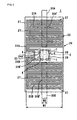
- the wireless IC device includes a wireless IC chip 5 processing transmission and reception signals at predetermined frequencies, a feeder circuit board 20 having a feeder circuit 22 composed of a first coupler 23A and a second coupler 23B, including inductance elements including line electrodes 24A and 24B, and a first radiation plate 30A and a second radiation plate 30B, functioning as an antenna and arranged on a board 31 as an PET film.
- the wireless IC chip 5 is mounted on the feeder circuit board 20 and both the wireless IC chip 5 and the feeder circuit board 20 form an electromagnetic coupler module 1.
- the first and second radiation plates 30A and 30B are metal strips linearly arranged on the flexible film board 31, and function as a dipole antenna. Ends of each of the first and second radiation plates 30A and 30B are provided with first and second mounts 30A' and 30B' which respectively support a feeder circuit board 20.
- the feeder circuit board 20 is glued on the first and second mounts 30A' and 30B' using an adhesive agent unillustrated, and the first and second mounts 30A' and 30B' are electromagnetically coupled with first and second couplers 23A and 23B as described below.
- the feeder circuit board 20 includes line electrodes 24A and 24B meandering on the board 21 made of a PET film. Ends of the line electrodes 24A and 24B respectively serve as connection electrodes 24A' and 24B', and the other ends thereof are shortcircuited to each other via an electrode 25. Furthermore, electrodes 26 and 26 electrically floating are formed on the flexible film board 21.
- the line electrodes 24A and 24B and the radiation plates 30A and 30B are produced by gluing on boards 21 and 31 a metal thin film, made of an electrically conductive material, such as aluminum foil or copper foil, or by forming a metal plate of Al, Cu, Ag, or the like or a an electrically conductive paste on the boards 21 and 31.
- the wireless IC chip 5 includes a clock circuit, a logic circuit, a memory circuit, and the like, and stores necessary information. As illustrated in Fig. 3 , input and output terminal electrodes 6 and 6 and mounting terminal electrodes 7 and 7 are arranged on the bottom surface of the wireless IC chip 5. In the wireless IC chip 5, the input and output terminal electrodes 6 and 6 are electrically connected to the connection electrodes 24A' and 24B' of the line electrodes 24A and 24B via metal bumps of solder or Au. The mounting terminal electrodes 7 and 7 are electrically connected to electrodes 26 and 26 via metal bumps.
- the wireless IC device thus constructed is glued on a container of goods as a handling target of the RFID system.
- the wireless IC chip 5 communicates with a reader/writer via the feeder circuit 22 and the first and second radiation plates 30A and 30B using a high frequency signal on the UHF frequency band. More specifically, the wireless IC chip 5 is operated by the feeder circuit 22 in response to the high frequency signal received by the first and second radiation plates 30A and 30B. A response signal from the wireless IC chip 5 is then emitted via the feeder circuit 22 from the radiation plates 30A and 30B.
- the first mount 30A' of the first radiation plate 30A is electromagnetically coupled with the first coupler 23A and the second mount 30B' of the second radiation plate 30B is electromagnetically coupled with the second coupler 23B.
- Each of the line electrodes 24A and 24B forms a resonator circuit with the inductance thereof and a capacitance formed the lines thereof.
- the resonator circuit is electromagnetically coupled with each of the first mount 30A' and the second mount 30B'.
- the resonator circuit performs impedance matching and determines a resonance frequency of a signal between the wireless IC chip 5 and each of the radiation plates 30A and 30B.
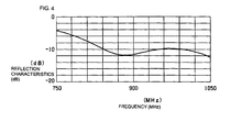
- Fig. 4 illustrates reflection characteristics of the wireless IC device. Excellent reflection characteristics equal to or higher than 10 dB are obtained in 900 MHz band.
- the infinitesimal wireless IC chip 5 is electrically connected to and mounted on the small feeder circuit board 20.
- the mounting of the wireless IC chip 5 is easy.
- the feeder electrode 22 is not directly electrically connected to the first and second radiation plates 30A and 30B, and the first and second couplers 23A and 23B are electromagnetically coupled with the first and second mounts 30A' and 30B'.
- the mounting accuracy with which the feeder circuit board 20 is mounted on (glued on with an adhesive agent) the first and second radiation plates 30A and 30B is eased.
- the feeder electrode 22 can also be miniaturized.
- the operating frequency of the wireless IC device is determined by the resonator circuit contained in the feeder circuit 22 and thus does not depend on the length of the radiation plates 30A and 30B. Even if the feeder circuit board 20 is mounted on the first and second mounts 30A' and 30B' in some degree of deviation, no operational malfunction takes place. In this sense, as well, the mounting accuracy is eased.
- the feeder circuit 22 is not directly conductively connected to the first and second radiation plates 30A and 30B, the wireless IC chip 5 is prevented from being damaged by an electrostatic charge as an energy wave equal to or lower than 200 MHz entering via the radiation plates 30A and 30B.
- a width W1 of the first coupler 23A and the second coupler 23B is set to be larger than a width W2 of the first mount 30A' and the second mount 30B'.
- the first and second mounts 30A' and 30B' are easily aligned in position with the couplers 23A and 23B.
- the mounting accuracy of the feeder circuit board 20 with respect to the radiation plates 30A and 30B is further eased. This is also true of each of the following embodiments as illustrated.
- the wireless IC device is further miniaturized. Furthermore, the first coupler 23A and the first mount 30A' orthogonally cross each other and the second coupler 23B and the second mount 30B' orthogonally cross each other. Magnetic fields generated at the couplers 23A and 23B and at the mounts 30A' and 30B' are perpendicular to each other. With this arrangement, the magnetic fields are easily coupled with each other. A power transfer efficiency between the feeder circuit 22 and each of the radiation plates 30A and 30B is increased.
- the first coupler 23A and the second coupler 23B include the line electrodes 24A and 24B that are formed to be axisymmetrical with each other with respect to an axis C centered on the wireless IC chip 5.
- the first and second mounts 30A' and 30B' are coupled with the feeder circuit 22 at the same constant, and the first radiation plate 30A and the second radiation plate 30B can have the same radiation characteristics and the same directivity characteristics. The same is true of the embodiments as illustrated below.
- the feeder circuit 22 can be produced in a compact form.
- the feeder circuit board 20 is also miniaturized.
- Fig. 5 illustrates a wireless IC device of a second embodiment of the present invention.
- the wireless IC device includes the meandering line electrodes 24A and 24B formed as the first coupler 23A and the second coupler 23B of the feeder circuit 22 arranged on the feeder circuit board 20.
- the line electrodes 24A and 24B are partially branched (branch points are denoted by reference numerals 27).
- the rest of the structure of the second embodiment is identical to the structure of the first embodiment.
- the line electrodes 24A and 24B are branched, and the branched portions are different in length.
- the first coupler 23A and the second coupler 23B thus provide a plurality of different frequencies. Frequencies of peak gains of the first and second radiation plates 30A and 30B functioning as the antennas are varied. Wide-band gain characteristics thus result.
- the rest of the operation and advantages is identical to the operation and advantages of the first embodiment.
- Fig. 6 illustrates a wireless IC device of a third embodiment of the present invention.
- the wireless IC device includes the meandering line electrodes 24A and 24B formed as the first coupler 23A and the second coupler 23B of the feeder circuit 22 arranged on the feeder circuit board 20.
- the line electrodes 24A and 24B here are bent to extend and meander within a rectangular shape along the longitudinal direction of the board 21.
- the first mount 30A' of the first radiation plate 30A and the second mount 30B' of the second radiation plate 30B have the letter T shape, and respectively orthogonally cross the first coupler 23A and the second coupler 23B in plan view.
- Fig. 7 illustrates a wireless IC device of a fourth embodiment of the present invention.
- the wireless IC device includes the spiraling line electrodes 24A and 24B formed as the first coupler 23A and the second coupler 23B of the feeder circuit 22 arranged on the feeder circuit board 20.
- the first mount 30A' of the first radiation plate 30A and the second mount 30B' of the second radiation plate 30B have the letter T shape.
- the rest of the structure of the fourth embodiment is identical to the structure of the first embodiment.
- the operation and advantages of the fourth embodiment are also identical to the operation and advantages of the first embodiment.
- the use of the first and second spiraling couplers 23A and 23B allows the feeder circuit 22 to be designed in a compact form and the feeder circuit board 20 to be miniaturized. Since areas where the first and second couplers 23A and 23B orthogonally cross the first and second mounts 30A' and 30B' are increased, the degree of coupling between the magnetic fields generated by the couplers 23A and 23B and the mounts 30A' and 30B' is increased.
- Fig. 8 illustrates a wireless IC device of a fifth embodiment of the present invention.
- the wireless IC device includes the line electrodes 24A and 24B that are formed by doubly spiraling the feeder circuit 22 arranged on the feeder circuit board 20.
- the line electrodes 24A and 24B are folded back at electrodes 28A and 28B with the ends thereof shortcircuited to each other.
- the rest of the structure of the fifth embodiment is identical to the structure of the first embodiment, and the operation and advantages of the fifth embodiment are also identical to the operation and advantages of the first embodiment.
- the line lengths of the line electrodes 24A and 24B are made different by doubling spiraling the line electrodes 24A and 24B or by branching the line electrodes 24A and 24B at predetermined positions as discussed with reference to the second embodiment.
- the resonance frequencies thereof can be made different by introducing a difference in a line width or an inter-electrode capacitance.
- the inductance of each electrode can be varied by changing the width of the electrode. More specifically, the larger the electrode width, the greater the inductance of the electrode.
- the inter-electrode capacitance can be varied by changing the spacing between the electrodes. More specifically, the greater the electrode spacing, the smaller the capacitance becomes.
- the resonance frequency can be fine-adjusted by changing the line width and/or the electrode spacing.
- Figs. 9 and 10 illustrate a wireless IC device of a sixth embodiment of the present invention.
- the wireless IC device includes the electromagnetic coupler module 1 composed of the wireless IC chip 5 and the feeder circuit board 20.
- the first mount 30A' of the first radiation plate 30A is electromagnetically coupled with the first coupler 23A of the feeder circuit 22 and the second mount 30B' of the second radiation plate 30B is electromagnetically coupled with the second coupler 23B.
- the feeder electrode 22 formed on the feeder circuit board 20 is identical to the counterpart in the first embodiment.
- the first and second radiation plates 30A and 30B are constructed of meandering metal strips on the flexible board 31.
- the first mount 30A' and the second mount 30B' formed on ends of the first and second radiation plates 30A and 30B overlap and cross the first coupler 23A and the second coupler 23B forming the line electrodes 24A and 24B for electromagnetic coupling, and the other ends of each the first and second radiation plates 30A and 30B are terminated with closed loops.
- the rest of the structure of the sixth embodiment is identical to the structure of the first embodiment.
- the operation and advantages of the sixth embodiment are identical to the operation and advantages of the first embodiment.
- the use of the first and second meandering radiation plates 30A and 30B allows the radiation plates 30A and 30B to be in a compact form.
- Figs. 11 and 12 illustrates a wireless IC device of a seventh embodiment of the present invention.
- the wireless IC device includes the electromagnetic coupler module 1 composed of the wireless IC chip 5 and the feeder circuit board 20.
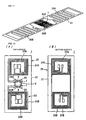
- the feeder electrode 22 is formed on the top surface and the bottom surface of the board 21 and the first and second mounts 30A' and 30B' formed at ends of the first and second meandering radiation plates 30A and 30B are meshed.
- the first and second couplers 23A and 23B including the spiraling line electrodes 24A and 24B are formed on the top surface of the board 21, and also the first and second couplers 23A and 23B including the spiraling line electrodes 24A and 24B are formed on the bottom surface of the board 21.
- the first and second couplers 23A and 23B formed on the top surface and the bottom surface of the board 21 are respectively electromagnetically coupled.
- the bottom surface of the flexible film board 21 is glued on the first and second mounts 30A' and 30B' of the first and second radiation plates 30A and 30B with an unillustrated adhesive agent.
- the first coupler 23A is electromagnetically coupled with the first mount 30A'
- the second coupler 23B is electromagnetically coupled with the second mount 30B'.
- the operation and advantages of the seventh embodiment are identical to the operation and advantages of the first embodiment. Since in particular the first and second couplers 23A and 23B are formed on both the top surface and the bottom surface, design flexibility of the line electrodes 24A and 24B (inductance elements) forming the feeder circuit 22 is increased, and the feeder circuit 22 is thus miniaturized. Since the first and second mounts 30A' and 30B' of the first and second radiation plates 30A and 30B are meshed, the magnetic flux generated by the feeder circuit 22 passes through apertures of the mounts. A change (reduction) in the magnetic flux is reduced. Since more magnetic flux passes through the mounts 30A' and 30B', transfer efficiency of signal energy is increased.
- the line electrodes 24A and 24B of the first and second couplers 23A and 23B are formed on the top and bottom surfaces of the flexible film board 21.
- One of the first and second couplers 23A and 23B may be formed on both the top and bottom surfaces of the board 21.
- one of the first and second mounts 30A' and 30B' may be meshed.
- the width of the first coupler and the second coupler is preferably larger than the width of the first mount and the second mount. This arrangement facilitates the position alignment between the mount and the coupler. The mounting accuracy of the feeder circuit board with respect to the mount is eased.
- the first coupler and the first mount may partially overlap each other in plan view and the second coupler and the second mount may partially overlap each other in plan view.
- the wireless IC device can be further miniaturized. If the two elements cross each other, the magnetic fields of the two elements are easily coupled and the transfer efficiency of power between the feeder circuit and the radiation plate is increased.
- At least one of the first mount and the second mount may be meshed. Since the magnetic flux generated by the feeder circuit passes through the apertures, a change (reduction) in the magnetic flux is reduced. Since more magnetic flux passes through the mounts, transfer efficiency of signal energy is increased.
- At least one of the first coupler and the second coupler may be formed on both the top and bottom surfaces of the feeder circuit board. With the coupler formed on both the top and bottom surfaces of the feeder circuit board, the design flexibility of the inductance element forming the feeder circuit is increased. The feeder circuit is thus miniaturized.
- first coupler and the second coupler may be axisymmetrical to each other with respect to the center of the wireless IC chip.
- the first and second radiation plates are coupled with the feeder circuit with the same constant.
- the first and second radiation plates can have the same radiation characteristics and the same directivity characteristics.
- Each of the first coupler and the second coupler may be constructed of a continuous line electrode, or a line electrode meandering or spiraling.
- the line electrode may be branched at a predetermined position.
- the meandering structure or the spiraling structure allows the feeder circuit to be produced in a compact form, thereby contributing to a miniaturization of the feeder circuit board. If the lengths of the line electrodes are varied, a plurality of resonance frequencies are provided. The frequencies of the peak gains of the first and second radiation plates functioning the antenna are varied, and wide-band gain characteristics are obtained.
- the resonance frequency of the line electrode is determined by the line length thereof. Even if the line lengths of the line electrodes are different, the resonance frequencies of the line electrodes can be made different by making different the inter-electrode capacitances or the like. More specifically, the inductance of the electrode is varied by changing the line width of the line electrode. The capacitance of the inter-electrode is varied by changing the electrode spacing.
- the feeder circuit board may be a flexible board. Since the flexible board is typically thin, the wireless IC device may be produced in a low-profile structure.
- the wireless IC device of the present invention is not limited to the above-described embodiments, and a variety of modification may be implemented in the invention without departing from the scope of the invention.
- the materials of the line electrodes 24A and 24B, the radiation plates 30A and 30B, and the boards 21 and 31 are described for exemplary purposes only. Any material can be used as long as the material has the required characteristics.
- the wireless IC chip 5 may be connected to the feeder circuit 22 through another process different from the one using the metal bump.
- the present invention is useful for the wireless IC device, and is particularly advantageous in that miniaturization is achieved without the need for high-precision mounting.
Landscapes
- Engineering & Computer Science (AREA)
- Microelectronics & Electronic Packaging (AREA)
- Computer Hardware Design (AREA)
- Physics & Mathematics (AREA)
- General Physics & Mathematics (AREA)
- Theoretical Computer Science (AREA)
- Details Of Aerials (AREA)
- Variable-Direction Aerials And Aerial Arrays (AREA)
- Junction Field-Effect Transistors (AREA)
- Devices For Checking Fares Or Tickets At Control Points (AREA)
- Credit Cards Or The Like (AREA)
Abstract
Description
- The present invention relates to wireless IC devices and, in particular, to a wireless IC device containing a wireless IC chip for use in an RFID (Radio Frequency Identification) system.
- RFID systems for transmitting information have recently been developed as a management system of goods. In such an RFID system, a reader/writer generating an induction electromagnetic field communicates in a contactless fashion with an IC chip (also referred to as an IC tag or a wireless IC chip) storing predetermined information attached to goods or a container.
- As disclosed in
Patent Document 1, a wireless tag known as a wireless IC device includes an IC chip mounted thereon. The wireless tag includes a dipole antenna (including a pair of main antenna elements and a matching unit) on a piezoelectric substrate and a tag IC electrically connected to ends of the dipole antenna. The matching unit, arranged between the tag IC and the main antenna elements, has a function of matching impedances between the tag IC and the main antenna elements. - The wireless tag has a problem discussed below. When the tag IC is electrically connected to the dipole antenna, a connection terminal of a small tag IC needs to be accurately positioned with respect to the dipole antenna and then mounted. A high precision mounting apparatus is thus required to avoid connection failures. Matching units, each occupying a large area, need to be arranged for the pair of main antenna elements in a manner such that the matching units do not overlap the antennas. The wireless tag may become larger in size.
- Patent Document 1: Japanese Unexamined Patent Application Publication (Translation of PCT Application) No.
2005-244778 - It is thus an object of the present invention to provide a wireless IC device miniaturized without the need for high precision mounting and appropriate for use in an RFID system.
- To achieve the above object, a wireless IC device as one embodiment of the present invention includes a wireless IC chip, having input and output terminals, for processing transmission and reception signals, a feeder circuit board including a feeder circuit, the feeder circuit including a resonator circuit and/or a matching circuit, the feeder circuit including a first coupler and a second coupler, each coupler including an inductance element, and a first radiation plate including a first mount having the feeder circuit board mounted thereon, and a second radiation plate including a second mount having the feeder circuit board mounted thereon, each radiation plate made of a metal. An electromagnetic coupler module having the feeder circuit board and the wireless IC chip mounted on the feeder circuit board is arranged with the input and output terminals of the wireless IC chip electrically connected to the feeder circuit. The first coupler is electromagnetically coupled with the first mount and the second coupler is electromagnetically mounted with the second mount. The wireless IC chip is operated by the first and second couplers in response to a signal received by the first and second radiation plates, and a response signal from the wireless IC chip is radiated to the outside from the first and second radiation plates via the first and second couplers.
- In the wireless IC device, the first and second radiation plates include the first and second mounts for mounting the feeder circuit board thereon. The feeder circuit composed of the first and second couplers electromagnetically coupled with the first and second mounts performs impedance matching between the wireless IC chip and the first and second radiation plate and/or sets a resonance frequency of a signal. The wireless IC chip is not connected to the large radiation plate, but electrically connected to and mounted on the small feeder circuit board. The mounting of the wireless IC chip is thus easy. The feeder circuit is not directly electrically connected to the first and second radiation plates, and the first and second couplers are electromagnetically coupled with the first and second mounts. Accuracy level required when the feeder circuit board is mounted on the radiation plate is eased. Since a single feeder circuit is used, the feeder circuit board can be miniaturized. Since the feeder circuit is not directly connected to the radiation plate, the wireless IC chip is prevented from being broken down even if an electrostatic charge enters via the radiation plate.
- An operating frequency of the wireless IC chip is determined by the feeder circuit (resonator circuit) arranged on the feeder circuit board, and does not depend on the length and size of the first and second mounts where the first and second radiation plates are coupled with the feeder circuit (resonator circuit). Operation error does not occur even if the mounting position of the feeder circuit board with respect to the first and second radiation plates are deviated to some degree on the feeder circuit board. The mounting accuracy is thus eased.
- Moreover, the wireless IC chip may have an information rewritable function in addition to the function of storing a variety of information related to the goods to which the wireless IC device is attached, and further may have a information processing function other than the function of the RFID system.
- In accordance with the present invention, the electromagnetic coupler module is constructed by arranging the feeder circuit, composed of the first coupler and the second coupler, on the feeder circuit board, and mounting the wireless IC chip on the feeder circuit board. The first and second couplers are thus electromagnetically coupled with the first and second mounts on the first and second radiation plates. This arrangement eliminates the need for mounting the wireless IC chip and the feeder circuit board with high accuracy, and the wireless IC device can be miniaturized.
-
- [
Fig. 1] Fig. 1 is a perspective view illustrating a wireless IC device in accordance with a first embodiment of the present invention. - [
Fig. 2] Fig. 2 is a plan view illustrating an electromagnetic coupler module in accordance with the first embodiment. - [
Fig. 3] Fig. 3 is a perspective view illustrating a wireless IC chip. - [
Fig. 4] Fig. 4 is a graph representing reflection characteristics of the first embodiment. - [
Fig. 5] Fig. 5 is a plan view illustrating the electromagnetic coupler module in a wireless IC device in accordance with a second embodiment of the present invention. - [
Fig. 6] Fig. 6 is a plan view illustrating the electromagnetic coupler module in a wireless IC device in accordance with a third embodiment of the present invention. - [
Fig. 7] Fig. 7 is a plan view illustrating the electromagnetic coupler module in a wireless IC device in accordance with a fourth embodiment of the present invention. [Fig. 8] Fig. 8 is a plan view illustrating the electromagnetic coupler module in a wireless IC device in accordance with a fifth embodiment of the present invention. - [
Fig. 9] Fig. 9 is a plan view illustrating a wireless IC device in accordance with a sixth embodiment of the present invention. - [
Fig. 10] Fig. 10 is a plan view illustrating the electromagnetic coupler module of the sixth embodiment. [Fig. 11] Fig. 11 is a perspective view illustrating a wireless IC device in accordance with a seventh embodiment of the present invention. - [
Fig. 12] Fig. 12 illustrates the electromagnetic coupler module of the seventh embodiment whereinFig. 12(A) is a plan view of the module andFig. 12(B) is a bottom view of the module. -
- 1
- Electromagnetic coupler module
- 5
- Wireless IC chip
- 6
- Input-output terminal electrodes
- 20
- Feeder circuit board
- 21
- Film board
- 22
- Feeder circuit
- 23A
- First coupler
- 23B
- Second coupler
- 24A and 24B
- ine electrodes
- 30A
- First radiation plate
- 30B
- Second radiation plate
- 30A'
- First mount
- 30B'
- Second mount
- The embodiments of a wireless IC device of the present invention are described with reference to the accompanying drawings. In the drawings, like elements are designed with like reference numerals and the discussion thereof is not duplicated.
-
Figs. 1 ,2 and 3 illustrate a first embodiment of the wireless IC device. The wireless IC device includes awireless IC chip 5 processing transmission and reception signals at predetermined frequencies, afeeder circuit board 20 having afeeder circuit 22 composed of afirst coupler 23A and asecond coupler 23B, including inductance elements includingline electrodes first radiation plate 30A and asecond radiation plate 30B, functioning as an antenna and arranged on aboard 31 as an PET film. Thewireless IC chip 5 is mounted on thefeeder circuit board 20 and both thewireless IC chip 5 and thefeeder circuit board 20 form anelectromagnetic coupler module 1. - The first and
second radiation plates flexible film board 31, and function as a dipole antenna. Ends of each of the first andsecond radiation plates second mounts 30A' and 30B' which respectively support afeeder circuit board 20. Thefeeder circuit board 20 is glued on the first andsecond mounts 30A' and 30B' using an adhesive agent unillustrated, and the first andsecond mounts 30A' and 30B' are electromagnetically coupled with first andsecond couplers - The
feeder circuit board 20 includesline electrodes board 21 made of a PET film. Ends of theline electrodes connection electrodes 24A' and 24B', and the other ends thereof are shortcircuited to each other via anelectrode 25. Furthermore,electrodes flexible film board 21. - The
line electrodes radiation plates boards 21 and 31 a metal thin film, made of an electrically conductive material, such as aluminum foil or copper foil, or by forming a metal plate of Al, Cu, Ag, or the like or a an electrically conductive paste on theboards - The
wireless IC chip 5 includes a clock circuit, a logic circuit, a memory circuit, and the like, and stores necessary information. As illustrated inFig. 3 , input andoutput terminal electrodes terminal electrodes wireless IC chip 5. In thewireless IC chip 5, the input andoutput terminal electrodes connection electrodes 24A' and 24B' of theline electrodes terminal electrodes electrodes - The wireless IC device thus constructed is glued on a container of goods as a handling target of the RFID system. The
wireless IC chip 5 communicates with a reader/writer via thefeeder circuit 22 and the first andsecond radiation plates wireless IC chip 5 is operated by thefeeder circuit 22 in response to the high frequency signal received by the first andsecond radiation plates wireless IC chip 5 is then emitted via thefeeder circuit 22 from theradiation plates - More in detail, the
first mount 30A' of thefirst radiation plate 30A is electromagnetically coupled with thefirst coupler 23A and thesecond mount 30B' of thesecond radiation plate 30B is electromagnetically coupled with thesecond coupler 23B. Each of theline electrodes first mount 30A' and thesecond mount 30B'. The resonator circuit performs impedance matching and determines a resonance frequency of a signal between thewireless IC chip 5 and each of theradiation plates -
Fig. 4 illustrates reflection characteristics of the wireless IC device. Excellent reflection characteristics equal to or higher than 10 dB are obtained in 900 MHz band. - In the wireless IC device, the infinitesimal
wireless IC chip 5 is electrically connected to and mounted on the smallfeeder circuit board 20. The mounting of thewireless IC chip 5 is easy. Thefeeder electrode 22 is not directly electrically connected to the first andsecond radiation plates second couplers second mounts 30A' and 30B'. The mounting accuracy with which thefeeder circuit board 20 is mounted on (glued on with an adhesive agent) the first andsecond radiation plates feeder electrode 22 can also be miniaturized. - The operating frequency of the wireless IC device is determined by the resonator circuit contained in the
feeder circuit 22 and thus does not depend on the length of theradiation plates feeder circuit board 20 is mounted on the first andsecond mounts 30A' and 30B' in some degree of deviation, no operational malfunction takes place. In this sense, as well, the mounting accuracy is eased. - Furthermore, since the
feeder circuit 22 is not directly conductively connected to the first andsecond radiation plates wireless IC chip 5 is prevented from being damaged by an electrostatic charge as an energy wave equal to or lower than 200 MHz entering via theradiation plates - In accordance with the first embodiment, a width W1 of the
first coupler 23A and thesecond coupler 23B is set to be larger than a width W2 of thefirst mount 30A' and thesecond mount 30B'. In this way, the first andsecond mounts 30A' and 30B' are easily aligned in position with thecouplers feeder circuit board 20 with respect to theradiation plates - Since the
first coupler 23A and thefirst mount 30A' overlap each other in plan view and thesecond coupler 23B and thesecond mount 30B' overlap each other in plan view, the wireless IC device is further miniaturized. Furthermore, thefirst coupler 23A and thefirst mount 30A' orthogonally cross each other and thesecond coupler 23B and thesecond mount 30B' orthogonally cross each other. Magnetic fields generated at thecouplers mounts 30A' and 30B' are perpendicular to each other. With this arrangement, the magnetic fields are easily coupled with each other. A power transfer efficiency between thefeeder circuit 22 and each of theradiation plates - The
first coupler 23A and thesecond coupler 23B include theline electrodes wireless IC chip 5. In this way, the first andsecond mounts 30A' and 30B' are coupled with thefeeder circuit 22 at the same constant, and thefirst radiation plate 30A and thesecond radiation plate 30B can have the same radiation characteristics and the same directivity characteristics. The same is true of the embodiments as illustrated below. - Since the
first coupler 23A and thesecond coupler 23B are themeandering line electrodes feeder circuit 22 can be produced in a compact form. Thefeeder circuit board 20 is also miniaturized. -
Fig. 5 illustrates a wireless IC device of a second embodiment of the present invention. The wireless IC device includes themeandering line electrodes first coupler 23A and thesecond coupler 23B of thefeeder circuit 22 arranged on thefeeder circuit board 20. Theline electrodes - The operation and advantages of the second embodiment remain identical to those of the first embodiment. In particular, the
line electrodes first coupler 23A and thesecond coupler 23B thus provide a plurality of different frequencies. Frequencies of peak gains of the first andsecond radiation plates -
Fig. 6 illustrates a wireless IC device of a third embodiment of the present invention. The wireless IC device includes themeandering line electrodes first coupler 23A and thesecond coupler 23B of thefeeder circuit 22 arranged on thefeeder circuit board 20. Theline electrodes board 21. Thefirst mount 30A' of thefirst radiation plate 30A and thesecond mount 30B' of thesecond radiation plate 30B have the letter T shape, and respectively orthogonally cross thefirst coupler 23A and thesecond coupler 23B in plan view. - The rest of the structure of the third embodiment remains identical to that of first embodiment, and the operation and advantages of the third embodiment are identical to the operation and advantage of the first embodiment.
-
Fig. 7 illustrates a wireless IC device of a fourth embodiment of the present invention. The wireless IC device includes the spiralingline electrodes first coupler 23A and thesecond coupler 23B of thefeeder circuit 22 arranged on thefeeder circuit board 20. As in the third embodiment, thefirst mount 30A' of thefirst radiation plate 30A and thesecond mount 30B' of thesecond radiation plate 30B have the letter T shape. - The rest of the structure of the fourth embodiment is identical to the structure of the first embodiment. The operation and advantages of the fourth embodiment are also identical to the operation and advantages of the first embodiment. In particular, the use of the first and
second spiraling couplers feeder circuit 22 to be designed in a compact form and thefeeder circuit board 20 to be miniaturized. Since areas where the first andsecond couplers second mounts 30A' and 30B' are increased, the degree of coupling between the magnetic fields generated by thecouplers mounts 30A' and 30B' is increased. -
Fig. 8 illustrates a wireless IC device of a fifth embodiment of the present invention. The wireless IC device includes theline electrodes feeder circuit 22 arranged on thefeeder circuit board 20. Theline electrodes electrodes - It is noted that the line lengths of the
line electrodes line electrodes line electrodes feeder circuit 22 corresponds to the line length of theline electrodes - Even if the lengths of the
line electrodes -
Figs. 9 and10 illustrate a wireless IC device of a sixth embodiment of the present invention. As in the first through fifth embodiments, the wireless IC device includes theelectromagnetic coupler module 1 composed of thewireless IC chip 5 and thefeeder circuit board 20. Thefirst mount 30A' of thefirst radiation plate 30A is electromagnetically coupled with thefirst coupler 23A of thefeeder circuit 22 and thesecond mount 30B' of thesecond radiation plate 30B is electromagnetically coupled with thesecond coupler 23B. - The
feeder electrode 22 formed on thefeeder circuit board 20 is identical to the counterpart in the first embodiment. The first andsecond radiation plates flexible board 31. Thefirst mount 30A' and thesecond mount 30B' formed on ends of the first andsecond radiation plates first coupler 23A and thesecond coupler 23B forming theline electrodes second radiation plates - The rest of the structure of the sixth embodiment is identical to the structure of the first embodiment. The operation and advantages of the sixth embodiment are identical to the operation and advantages of the first embodiment. In particular, the use of the first and second meandering
radiation plates radiation plates -
Figs. 11 and 12 illustrates a wireless IC device of a seventh embodiment of the present invention. As in the first through sixth embodiments, the wireless IC device includes theelectromagnetic coupler module 1 composed of thewireless IC chip 5 and thefeeder circuit board 20. Thefeeder electrode 22 is formed on the top surface and the bottom surface of theboard 21 and the first andsecond mounts 30A' and 30B' formed at ends of the first and second meanderingradiation plates - More in detail, as illustrated in
Figs. 12(A) and 12(B) , the first andsecond couplers line electrodes board 21, and also the first andsecond couplers line electrodes board 21. The first andsecond couplers board 21 are respectively electromagnetically coupled. The bottom surface of theflexible film board 21 is glued on the first andsecond mounts 30A' and 30B' of the first andsecond radiation plates first coupler 23A is electromagnetically coupled with thefirst mount 30A', and thesecond coupler 23B is electromagnetically coupled with thesecond mount 30B'. - The operation and advantages of the seventh embodiment are identical to the operation and advantages of the first embodiment. Since in particular the first and
second couplers line electrodes feeder circuit 22 is increased, and thefeeder circuit 22 is thus miniaturized. Since the first andsecond mounts 30A' and 30B' of the first andsecond radiation plates feeder circuit 22 passes through apertures of the mounts. A change (reduction) in the magnetic flux is reduced. Since more magnetic flux passes through themounts 30A' and 30B', transfer efficiency of signal energy is increased. - In the seventh embodiment, the
line electrodes second couplers flexible film board 21. One of the first andsecond couplers board 21. Furthermore, one of the first andsecond mounts 30A' and 30B' may be meshed. - In the wireless IC device, the width of the first coupler and the second coupler is preferably larger than the width of the first mount and the second mount. This arrangement facilitates the position alignment between the mount and the coupler. The mounting accuracy of the feeder circuit board with respect to the mount is eased.
- The first coupler and the first mount may partially overlap each other in plan view and the second coupler and the second mount may partially overlap each other in plan view. With the two elements overlapping each other in plan view, the wireless IC device can be further miniaturized. If the two elements cross each other, the magnetic fields of the two elements are easily coupled and the transfer efficiency of power between the feeder circuit and the radiation plate is increased.
- At least one of the first mount and the second mount may be meshed. Since the magnetic flux generated by the feeder circuit passes through the apertures, a change (reduction) in the magnetic flux is reduced. Since more magnetic flux passes through the mounts, transfer efficiency of signal energy is increased.
- At least one of the first coupler and the second coupler may be formed on both the top and bottom surfaces of the feeder circuit board. With the coupler formed on both the top and bottom surfaces of the feeder circuit board, the design flexibility of the inductance element forming the feeder circuit is increased. The feeder circuit is thus miniaturized.
- Furthermore, the first coupler and the second coupler may be axisymmetrical to each other with respect to the center of the wireless IC chip. The first and second radiation plates are coupled with the feeder circuit with the same constant. The first and second radiation plates can have the same radiation characteristics and the same directivity characteristics.
- Each of the first coupler and the second coupler may be constructed of a continuous line electrode, or a line electrode meandering or spiraling. The line electrode may be branched at a predetermined position. The meandering structure or the spiraling structure allows the feeder circuit to be produced in a compact form, thereby contributing to a miniaturization of the feeder circuit board. If the lengths of the line electrodes are varied, a plurality of resonance frequencies are provided. The frequencies of the peak gains of the first and second radiation plates functioning the antenna are varied, and wide-band gain characteristics are obtained.
- The resonance frequency of the line electrode is determined by the line length thereof. Even if the line lengths of the line electrodes are different, the resonance frequencies of the line electrodes can be made different by making different the inter-electrode capacitances or the like. More specifically, the inductance of the electrode is varied by changing the line width of the line electrode. The capacitance of the inter-electrode is varied by changing the electrode spacing.
- The feeder circuit board may be a flexible board. Since the flexible board is typically thin, the wireless IC device may be produced in a low-profile structure.
- The wireless IC device of the present invention is not limited to the above-described embodiments, and a variety of modification may be implemented in the invention without departing from the scope of the invention.
- The materials of the
line electrodes radiation plates boards wireless IC chip 5 may be connected to thefeeder circuit 22 through another process different from the one using the metal bump. - As described above, the present invention is useful for the wireless IC device, and is particularly advantageous in that miniaturization is achieved without the need for high-precision mounting.
Claims (12)
- A wireless IC device, comprising:a wireless IC chip, having input and output terminals, for processing transmission and reception signals,a feeder circuit board including a feeder circuit, the feeder circuit including a resonator circuit and/or a matching circuit, the feeder circuit including a first coupler and a second coupler, each coupler including an inductance element, anda first radiation plate including a first mount having the feeder circuit board mounted thereon, and a second radiation plate including a second mount having the feeder circuit board mounted thereon, each radiation plate made of a metal,wherein an electromagnetic coupler module having the feeder circuit board and the wireless IC chip mounted on the feeder circuit board is arranged with the input and output terminals of the wireless IC chip electrically connected to the feeder circuit,
wherein the first coupler is electromagnetically coupled with the first mount and the second coupler is electromagnetically mounted with the second mount, and
wherein the wireless IC chip is operated by the first and second couplers in response to a signal received by the first and second radiation plates, and a response signal from the wireless IC chip is radiated to the outside from the first and second radiation plates via the first and second couplers. - The wireless IC device according to claim 1, wherein a width of the first coupler and the second coupler is larger than a width of the first mount and the second mount.
- The wireless IC device according to one of claims 1 and 2, wherein the first coupler and the first mount partially overlap each other in plan view and the second coupler and the second mount partially overlap each other in plan view.
- The wireless IC device according to one of claims 1 through 3, wherein the first coupler and the first mount orthogonally cross each other in plan view and the second coupler and the second mount orthogonally cross each other in plan view.
- The wireless IC device according to one of claims 1 through 4, wherein at least one of the first mount and the second mount is meshed.
- The wireless IC device according to one of claims 1 through 5, wherein at least one of the first coupler and the second coupler is formed on the top surface and the bottom surface of the feeder circuit board.
- The wireless IC device according to one of claims 1 through 6, wherein the first coupler and the second coupler are formed of line electrodes axisymmetrical to each other with respect to the wireless IC chip.
- The wireless IC device according to one of claims 1 through 7, wherein each of the first coupler and the second coupler is a continuous line electrode.
- The wireless IC device according to one of claims 1 through 8, wherein each of the first coupler and the second coupler is a meandering line electrode.
- The wireless IC device according to one of claims 1 through 8, wherein each of the first coupler and the second coupler is a spiraling line electrode.
- The wireless IC device according to one of claims 1 through 10, wherein each of the first coupler and the second coupler is a line electrode, the line electrode branching at a predetermined position.
- The wireless IC device according to one of claims 1 through 11, wherein the feeder circuit board is a flexible board.
Applications Claiming Priority (3)
| Application Number | Priority Date | Filing Date | Title |
|---|---|---|---|
| JP2007168625 | 2007-06-27 | ||
| JP2007232844 | 2007-09-07 | ||
| PCT/JP2008/061442 WO2009001814A1 (en) | 2007-06-27 | 2008-06-24 | Wireless ic device |
Publications (3)
| Publication Number | Publication Date |
|---|---|
| EP2077602A1 true EP2077602A1 (en) | 2009-07-08 |
| EP2077602A4 EP2077602A4 (en) | 2010-08-18 |
| EP2077602B1 EP2077602B1 (en) | 2012-02-08 |
Family
ID=40185628
Family Applications (1)
| Application Number | Title | Priority Date | Filing Date |
|---|---|---|---|
| EP08790581A Active EP2077602B1 (en) | 2007-06-27 | 2008-06-24 | Wireless ic device |
Country Status (7)
| Country | Link |
|---|---|
| US (1) | US8264357B2 (en) |
| EP (1) | EP2077602B1 (en) |
| JP (1) | JP4396785B2 (en) |
| KR (1) | KR101062124B1 (en) |
| CN (1) | CN101558530B (en) |
| AT (1) | ATE545174T1 (en) |
| WO (1) | WO2009001814A1 (en) |
Cited By (1)
| Publication number | Priority date | Publication date | Assignee | Title |
|---|---|---|---|---|
| WO2016139394A1 (en) * | 2015-03-04 | 2016-09-09 | Smart Packaging Solutions (S.P.S.) | Microelectronic component for a contactless smart card |
Families Citing this family (13)
| Publication number | Priority date | Publication date | Assignee | Title |
|---|---|---|---|---|
| CN102498617B (en) * | 2009-09-09 | 2015-04-01 | 株式会社村田制作所 | Antenna, manufacturing method thereof, and wireless IC device |
| JP2011182392A (en) * | 2010-02-08 | 2011-09-15 | Sinfonia Technology Co Ltd | Dipole-type ic tag antenna, antenna roll and method of using ic tag |
| CN102403570B (en) * | 2010-09-10 | 2013-09-25 | 航天信息股份有限公司 | Tag antenna and electronic tag |
| US9299021B2 (en) * | 2010-11-11 | 2016-03-29 | Avery Dennison Corporation | RFID devices and methods for manufacturing |
| CN105048058B (en) * | 2011-01-05 | 2017-10-27 | 株式会社村田制作所 | Wireless communication devices |
| JP5418737B2 (en) * | 2011-09-09 | 2014-02-19 | 株式会社村田製作所 | Antenna apparatus and wireless device |
| CN103606002A (en) * | 2013-11-30 | 2014-02-26 | 陈其晖 | RFID electronic tag and antenna thereof |
| WO2016053951A1 (en) * | 2014-10-01 | 2016-04-07 | Ohio State Innovation Foundation | Stretchable broad impedance bandwidth rfid devices |
| KR102175750B1 (en) | 2014-10-29 | 2020-11-06 | 삼성전자주식회사 | Antenna device for electronic device with the same |
| CN104485508A (en) * | 2014-12-19 | 2015-04-01 | 夏景 | Complex impedance RFID (radio frequency identification) bow-tie-shaped printing antenna |
| US9887464B2 (en) * | 2015-10-22 | 2018-02-06 | Ajou University Industry-Academic Cooperation Foundation | Compact dipole antenna for RFID tag |
| WO2019017022A1 (en) * | 2017-07-21 | 2019-01-24 | 株式会社村田製作所 | Wireless communication device |
| CN109728403B (en) * | 2018-12-28 | 2023-09-01 | 浙江中烟工业有限责任公司 | Single-port feed dual-polarized far-field/near-field antenna for forklift reader |
Family Cites Families (210)
| Publication number | Priority date | Publication date | Assignee | Title |
|---|---|---|---|---|
| US3364564A (en) | 1965-06-28 | 1968-01-23 | Gregory Ind Inc | Method of producing welding studs dischargeable in end-to-end relationship |
| JPS5754964B2 (en) | 1974-05-08 | 1982-11-20 | ||
| JPS6193701A (en) | 1984-10-13 | 1986-05-12 | Toyota Motor Corp | Antenna system for automobile |
| JPS62127140U (en) | 1986-02-03 | 1987-08-12 | ||
| US5253969A (en) | 1989-03-10 | 1993-10-19 | Sms Schloemann-Siemag Aktiengesellschaft | Feeding system for strip material, particularly in treatment plants for metal strips |
| JP2662742B2 (en) | 1990-03-13 | 1997-10-15 | 株式会社村田製作所 | Bandpass filter |
| JP2763664B2 (en) | 1990-07-25 | 1998-06-11 | 日本碍子株式会社 | Wiring board for distributed constant circuit |
| JPH04150011A (en) | 1990-10-12 | 1992-05-22 | Tdk Corp | Composite electronic component |
| NL9100176A (en) | 1991-02-01 | 1992-03-02 | Nedap Nv | Antenna configuration for contactless identification label - forms part of tuned circuit of ID or credit card interrogated via inductive coupling |
| NL9100347A (en) | 1991-02-26 | 1992-03-02 | Nedap Nv | Integrated transformer circuit for ID or credit card - is interrogated via contactless inductive coupling using capacitor to form tuned circuit |
| JPH04321190A (en) | 1991-04-22 | 1992-11-11 | Mitsubishi Electric Corp | Antenna circuit and its production for non-contact type portable storage |
| DE69215283T2 (en) | 1991-07-08 | 1997-03-20 | Nippon Telegraph & Telephone | Extendable antenna system |
| JPH05327331A (en) | 1992-05-15 | 1993-12-10 | Matsushita Electric Works Ltd | Printed antenna |
| JP3186235B2 (en) | 1992-07-30 | 2001-07-11 | 株式会社村田製作所 | Resonator antenna |
| JPH0677729A (en) | 1992-08-25 | 1994-03-18 | Mitsubishi Electric Corp | Microwave circuit with integrated antenna |
| JPH06177635A (en) | 1992-12-07 | 1994-06-24 | Mitsubishi Electric Corp | Cross dipole antenna system |
| JPH07183836A (en) | 1993-12-22 | 1995-07-21 | San'eisha Mfg Co Ltd | Coupling filter device for distribution line carrier communication |
| US5491483A (en) | 1994-01-05 | 1996-02-13 | Texas Instruments Incorporated | Single loop transponder system and method |
| JP3427527B2 (en) | 1994-12-26 | 2003-07-22 | 凸版印刷株式会社 | Biodegradable laminate and biodegradable card |
| US6096431A (en) | 1994-07-25 | 2000-08-01 | Toppan Printing Co., Ltd. | Biodegradable cards |
| JP3141692B2 (en) | 1994-08-11 | 2001-03-05 | 松下電器産業株式会社 | Millimeter wave detector |
| JPH0887580A (en) | 1994-09-14 | 1996-04-02 | Omron Corp | Data carriers and ball games |
| JPH08279027A (en) | 1995-04-04 | 1996-10-22 | Toshiba Corp | Wireless communication card |
| US5955723A (en) | 1995-05-03 | 1999-09-21 | Siemens Aktiengesellschaft | Contactless chip card |
| JPH08307126A (en) | 1995-05-09 | 1996-11-22 | Kyocera Corp | Antenna storage structure |
| US5629241A (en) | 1995-07-07 | 1997-05-13 | Hughes Aircraft Company | Microwave/millimeter wave circuit structure with discrete flip-chip mounted elements, and method of fabricating the same |
| GB2305075A (en) | 1995-09-05 | 1997-03-26 | Ibm | Radio Frequency Tag for Electronic Apparatus |
| US6104611A (en) * | 1995-10-05 | 2000-08-15 | Nortel Networks Corporation | Packaging system for thermally controlling the temperature of electronic equipment |
| AUPO055296A0 (en) | 1996-06-19 | 1996-07-11 | Integrated Silicon Design Pty Ltd | Enhanced range transponder system |
| US6104311A (en) | 1996-08-26 | 2000-08-15 | Addison Technologies | Information storage and identification tag |
| ATE210864T1 (en) | 1996-10-09 | 2001-12-15 | Pav Card Gmbh | METHOD AND CONNECTION ARRANGEMENT FOR PRODUCING A CHIP CARD |
| DE19703029A1 (en) | 1997-01-28 | 1998-07-30 | Amatech Gmbh & Co Kg | Transmission module for a transponder device and transponder device and method for operating a transponder device |
| US6181287B1 (en) * | 1997-03-10 | 2001-01-30 | Precision Dynamics Corporation | Reactively coupled elements in circuits on flexible substrates |
| WO1999026195A1 (en) | 1997-11-14 | 1999-05-27 | Toppan Printing Co., Ltd. | Composite ic module and composite ic card |
| JP3800765B2 (en) | 1997-11-14 | 2006-07-26 | 凸版印刷株式会社 | Compound IC card |
| JPH11220319A (en) | 1998-01-30 | 1999-08-10 | Sharp Corp | Antenna device |
| JPH11261325A (en) | 1998-03-10 | 1999-09-24 | Shiro Sugimura | Coil element and manufacturing method thereof |
| EP0987789A4 (en) | 1998-03-31 | 2004-09-22 | Matsushita Electric Industrial Co Ltd | ANTENNA AND DIGITAL TELEVISION |
| US5936150A (en) | 1998-04-13 | 1999-08-10 | Rockwell Science Center, Llc | Thin film resonant chemical sensor with resonant acoustic isolator |
| CN1267267A (en) | 1998-04-14 | 2000-09-20 | 德克萨斯黎伯迪纸板箱公司 | Container for compressors and other goods |
| US6107920A (en) | 1998-06-09 | 2000-08-22 | Motorola, Inc. | Radio frequency identification tag having an article integrated antenna |
| JP2000021639A (en) | 1998-07-02 | 2000-01-21 | Sharp Corp | Inductor, resonance circuit, matching circuit, antenna circuit and oscillation circuit using the same |
| JP2000022421A (en) | 1998-07-03 | 2000-01-21 | Murata Mfg Co Ltd | Chip antenna and radio device mounted with it |
| JP2000311226A (en) | 1998-07-28 | 2000-11-07 | Toshiba Corp | Wireless IC card, manufacturing method thereof, and wireless IC card read / write system |
| EP0977145A3 (en) | 1998-07-28 | 2002-11-06 | Kabushiki Kaisha Toshiba | Radio IC card |
| JP2000059260A (en) | 1998-08-04 | 2000-02-25 | Sony Corp | Storage device |
| CN100492388C (en) | 1998-08-14 | 2009-05-27 | 3M创新有限公司 | Radio frequency identification system applications |
| DE69909301T2 (en) | 1998-08-14 | 2004-04-22 | 3M Innovative Properties Co., St. Paul | USE FOR A HIGH FREQUENCY IDENTIFICATION SYSTEM |
| JP4411670B2 (en) | 1998-09-08 | 2010-02-10 | 凸版印刷株式会社 | Non-contact IC card manufacturing method |
| JP4508301B2 (en) | 1998-09-16 | 2010-07-21 | 大日本印刷株式会社 | Non-contact IC card |
| JP3632466B2 (en) | 1998-10-23 | 2005-03-23 | 凸版印刷株式会社 | Inspection device and inspection method for non-contact IC card |
| JP3924962B2 (en) | 1998-10-30 | 2007-06-06 | 株式会社デンソー | ID tag for dishes |
| JP2000148948A (en) | 1998-11-05 | 2000-05-30 | Sony Corp | Non-contact type IC label and manufacturing method thereof |
| JP2000172812A (en) | 1998-12-08 | 2000-06-23 | Hitachi Maxell Ltd | Noncontact information medium |
| JP2000228602A (en) | 1999-02-08 | 2000-08-15 | Alps Electric Co Ltd | Resonance line |
| JP4349597B2 (en) | 1999-03-26 | 2009-10-21 | 大日本印刷株式会社 | IC chip manufacturing method and memory medium manufacturing method incorporating the same |
| JP2000286634A (en) | 1999-03-30 | 2000-10-13 | Ngk Insulators Ltd | Antenna system and its manufacture |
| US6542050B1 (en) | 1999-03-30 | 2003-04-01 | Ngk Insulators, Ltd. | Transmitter-receiver |
| JP3067764B1 (en) | 1999-03-31 | 2000-07-24 | 株式会社豊田自動織機製作所 | Mobile communication coupler, mobile body, and mobile communication method |
| JP2000321984A (en) | 1999-05-12 | 2000-11-24 | Hitachi Ltd | Label with RF-ID tag |
| JP3557130B2 (en) | 1999-07-14 | 2004-08-25 | 新光電気工業株式会社 | Method for manufacturing semiconductor device |
| JP2001043340A (en) | 1999-07-29 | 2001-02-16 | Toppan Printing Co Ltd | Composite IC card |
| US6259369B1 (en) | 1999-09-30 | 2001-07-10 | Moore North America, Inc. | Low cost long distance RFID reading |
| JP3451373B2 (en) | 1999-11-24 | 2003-09-29 | オムロン株式会社 | Manufacturing method of data carrier capable of reading electromagnetic wave |
| JP4186149B2 (en) | 1999-12-06 | 2008-11-26 | 株式会社エフ・イー・シー | Auxiliary antenna for IC card |
| JP2001240046A (en) | 2000-02-25 | 2001-09-04 | Toppan Forms Co Ltd | Container and manufacturing method thereof |
| JP2001256457A (en) | 2000-03-13 | 2001-09-21 | Toshiba Corp | Semiconductor device, manufacturing method thereof, and IC card communication system |
| JP4624537B2 (en) | 2000-04-04 | 2011-02-02 | 大日本印刷株式会社 | Non-contact data carrier device, storage |
| JP2001319380A (en) | 2000-05-11 | 2001-11-16 | Mitsubishi Materials Corp | Optical disk with RFID |
| JP2001331976A (en) | 2000-05-17 | 2001-11-30 | Casio Comput Co Ltd | Optical recording type recording medium |
| JP4223174B2 (en) | 2000-05-19 | 2009-02-12 | Dxアンテナ株式会社 | Film antenna |
| JP2001344574A (en) | 2000-05-30 | 2001-12-14 | Mitsubishi Materials Corp | Interrogator antenna device |
| JP2001352176A (en) | 2000-06-05 | 2001-12-21 | Fuji Xerox Co Ltd | Multilayer printed wiring board and manufacturing method of multilayer printed wiring board |
| JP2002024776A (en) | 2000-07-07 | 2002-01-25 | Nippon Signal Co Ltd:The | Ic card reader/writer |
| JP2002042076A (en) | 2000-07-21 | 2002-02-08 | Dainippon Printing Co Ltd | Non-contact data carrier and booklet having non-contact data carrier |
| JP3075400U (en) | 2000-08-03 | 2001-02-16 | 昌栄印刷株式会社 | Non-contact IC card |
| JP2002063557A (en) | 2000-08-21 | 2002-02-28 | Mitsubishi Materials Corp | Tag for rfid |
| JP2002076750A (en) | 2000-08-24 | 2002-03-15 | Murata Mfg Co Ltd | Antenna device and radio equipment equipped with it |
| JP4615695B2 (en) | 2000-10-19 | 2011-01-19 | 三星エスディーエス株式会社 | IC module for IC card and IC card using it |
| US6634564B2 (en) | 2000-10-24 | 2003-10-21 | Dai Nippon Printing Co., Ltd. | Contact/noncontact type data carrier module |
| JP4628611B2 (en) | 2000-10-27 | 2011-02-09 | 三菱マテリアル株式会社 | antenna |
| JP2002185358A (en) | 2000-11-24 | 2002-06-28 | Supersensor Pty Ltd | Method for fitting rf transponder to container |
| JP4641096B2 (en) | 2000-12-07 | 2011-03-02 | 大日本印刷株式会社 | Non-contact data carrier device and wiring member for booster antenna |
| JP2002183690A (en) | 2000-12-11 | 2002-06-28 | Hitachi Maxell Ltd | Non-contact IC tag device |
| US20060071084A1 (en) | 2000-12-15 | 2006-04-06 | Electrox Corporation | Process for manufacture of novel, inexpensive radio frequency identification devices |
| JP3788325B2 (en) | 2000-12-19 | 2006-06-21 | 株式会社村田製作所 | Multilayer coil component and manufacturing method thereof |
| TW531976B (en) | 2001-01-11 | 2003-05-11 | Hanex Co Ltd | Communication apparatus and installing structure, manufacturing method and communication method |
| JP3621655B2 (en) | 2001-04-23 | 2005-02-16 | 株式会社ハネックス中央研究所 | RFID tag structure and manufacturing method thereof |
| JP4662400B2 (en) | 2001-02-05 | 2011-03-30 | 大日本印刷株式会社 | Articles with coil-on-chip semiconductor modules |
| JP2002298109A (en) | 2001-03-30 | 2002-10-11 | Toppan Forms Co Ltd | Non-contact IC media and method of manufacturing the same |
| JP3570386B2 (en) | 2001-03-30 | 2004-09-29 | 松下電器産業株式会社 | Portable information terminal with built-in wireless function |
| EP1413004A4 (en) * | 2001-05-17 | 2004-07-21 | Cypress Semiconductor Corp | BALL MATRIX GRID ANTENNA |
| JP2005236339A (en) | 2001-07-19 | 2005-09-02 | Oji Paper Co Ltd | IC chip assembly |
| JP2002362613A (en) | 2001-06-07 | 2002-12-18 | Toppan Printing Co Ltd | Laminated packaging material in which non-contact IC is laminated, packaging container using the same, and method for detecting opening of packaging container |
| JP4710174B2 (en) | 2001-06-13 | 2011-06-29 | 株式会社村田製作所 | Balanced LC filter |
| JP4882167B2 (en) | 2001-06-18 | 2012-02-22 | 大日本印刷株式会社 | Card-integrated form with non-contact IC chip |
| JP2002373029A (en) | 2001-06-18 | 2002-12-26 | Hitachi Ltd | How to prevent unauthorized copying of software using IC tags |
| JP4759854B2 (en) | 2001-06-19 | 2011-08-31 | 株式会社寺岡精工 | Mounting method of IC tag to metal object and IC tag built-in marker |
| JP2003087008A (en) | 2001-07-02 | 2003-03-20 | Ngk Insulators Ltd | Multilayer dielectric filter |
| JP4058919B2 (en) | 2001-07-03 | 2008-03-12 | 日立化成工業株式会社 | Non-contact IC label, non-contact IC card, non-contact IC label or IC module for non-contact IC card |
| JP2003030612A (en) | 2001-07-19 | 2003-01-31 | Oji Paper Co Ltd | Ic chip mounting body |
| JP3629448B2 (en) | 2001-07-27 | 2005-03-16 | Tdk株式会社 | ANTENNA DEVICE AND ELECTRONIC DEVICE HAVING THE SAME |
| JP2003069335A (en) | 2001-08-28 | 2003-03-07 | Hitachi Kokusai Electric Inc | Auxiliary antenna |
| JP2003067711A (en) | 2001-08-29 | 2003-03-07 | Toppan Forms Co Ltd | Articles with IC chip mounting or antenna part |
| JP4514374B2 (en) | 2001-09-05 | 2010-07-28 | トッパン・フォームズ株式会社 | RF-ID inspection system |
| JP4747467B2 (en) | 2001-09-07 | 2011-08-17 | 大日本印刷株式会社 | Non-contact IC tag |
| JP2003085520A (en) | 2001-09-11 | 2003-03-20 | Oji Paper Co Ltd | IC card manufacturing method |
| JP4845306B2 (en) | 2001-09-25 | 2011-12-28 | トッパン・フォームズ株式会社 | RF-ID inspection system |
| JP4698096B2 (en) | 2001-09-25 | 2011-06-08 | トッパン・フォームズ株式会社 | RF-ID inspection system |
| JP2003110344A (en) | 2001-09-26 | 2003-04-11 | Hitachi Metals Ltd | Surface-mounting type antenna and antenna device mounting the same |
| JP2003132330A (en) | 2001-10-25 | 2003-05-09 | Sato Corp | RFID label printer |
| JP2003134007A (en) | 2001-10-30 | 2003-05-09 | Auto Network Gijutsu Kenkyusho:Kk | Signal transmission / reception system between vehicle-mounted devices and signal transmission / reception method between vehicle-mounted devices |
| JP3908514B2 (en) | 2001-11-20 | 2007-04-25 | 大日本印刷株式会社 | Package with IC tag and method of manufacturing package with IC tag |
| JP3984458B2 (en) | 2001-11-20 | 2007-10-03 | 大日本印刷株式会社 | Manufacturing method of package with IC tag |
| JP2003188338A (en) | 2001-12-13 | 2003-07-04 | Sony Corp | Circuit board device and method of manufacturing the same |
| JP3700777B2 (en) | 2001-12-17 | 2005-09-28 | 三菱マテリアル株式会社 | Electrode structure of RFID tag and method for adjusting resonance frequency using the electrode |
| JP4028224B2 (en) | 2001-12-20 | 2007-12-26 | 大日本印刷株式会社 | Paper IC card substrate having non-contact communication function |
| JP3895175B2 (en) | 2001-12-28 | 2007-03-22 | Ntn株式会社 | Dielectric resin integrated antenna |
| JP2003209421A (en) | 2002-01-17 | 2003-07-25 | Dainippon Printing Co Ltd | RFID tag having transparent antenna and method of manufacturing the same |
| JP3915092B2 (en) | 2002-01-21 | 2007-05-16 | 株式会社エフ・イー・シー | Booster antenna for IC card |
| JP2003216919A (en) | 2002-01-23 | 2003-07-31 | Toppan Forms Co Ltd | RF-ID media |
| JP2003233780A (en) | 2002-02-06 | 2003-08-22 | Mitsubishi Electric Corp | Data communication device |
| JP3998992B2 (en) | 2002-02-14 | 2007-10-31 | 大日本印刷株式会社 | Method for forming antenna pattern on IC chip mounted on web and package with IC tag |
| JP2003243918A (en) | 2002-02-18 | 2003-08-29 | Dainippon Printing Co Ltd | Non-contact IC tag antenna and non-contact IC tag |
| JP2003249813A (en) | 2002-02-25 | 2003-09-05 | Tecdia Kk | RFID tag with loop antenna |
| US7119693B1 (en) | 2002-03-13 | 2006-10-10 | Celis Semiconductor Corp. | Integrated circuit with enhanced coupling |
| JP2003288560A (en) | 2002-03-27 | 2003-10-10 | Toppan Forms Co Ltd | Interposer and inlet sheet having antistatic function |
| US7129834B2 (en) | 2002-03-28 | 2006-10-31 | Kabushiki Kaisha Toshiba | String wireless sensor and its manufacturing method |
| JP2003309418A (en) | 2002-04-17 | 2003-10-31 | Alps Electric Co Ltd | Dipole antenna |
| JP3879098B2 (en) | 2002-05-10 | 2007-02-07 | 株式会社エフ・イー・シー | Booster antenna for IC card |
| US6753814B2 (en) | 2002-06-27 | 2004-06-22 | Harris Corporation | Dipole arrangements using dielectric substrates of meta-materials |
| JP3863464B2 (en) | 2002-07-05 | 2006-12-27 | 株式会社ヨコオ | Filter built-in antenna |
| JP4107381B2 (en) | 2002-08-23 | 2008-06-25 | 横浜ゴム株式会社 | Pneumatic tire |
| JP2004096566A (en) | 2002-09-02 | 2004-03-25 | Toenec Corp | Inductive communication equipment |
| EP1594188B1 (en) | 2003-02-03 | 2010-04-14 | Panasonic Corporation | Antenna device and wireless communication device using same |
| EP1445821A1 (en) | 2003-02-06 | 2004-08-11 | Matsushita Electric Industrial Co., Ltd. | Portable radio communication apparatus provided with a boom portion |
| JP2004253858A (en) | 2003-02-18 | 2004-09-09 | Minerva:Kk | Booster antenna device for ic tag |
| JP4034676B2 (en) | 2003-03-20 | 2008-01-16 | 日立マクセル株式会社 | Non-contact communication type information carrier |
| JP2004297249A (en) | 2003-03-26 | 2004-10-21 | Matsushita Electric Ind Co Ltd | Coupler between different phases and its mounting method, and coupling method between different phases |
| JP2004297681A (en) | 2003-03-28 | 2004-10-21 | Toppan Forms Co Ltd | Non-contact information recording medium |
| JP2004326380A (en) | 2003-04-24 | 2004-11-18 | Dainippon Printing Co Ltd | RFID tag |
| JP2004334268A (en) | 2003-04-30 | 2004-11-25 | Dainippon Printing Co Ltd | Paper IC tags and books / magazines with paper IC tags, books with paper IC tags |
| JP2004336250A (en) | 2003-05-02 | 2004-11-25 | Taiyo Yuden Co Ltd | Antenna matching circuit, and mobile communication apparatus and dielectric antenna having the same |
| JP2004343000A (en) | 2003-05-19 | 2004-12-02 | Fujikura Ltd | Semiconductor module, non-contact IC tag having the same, and method of manufacturing semiconductor module |
| JP2004362190A (en) | 2003-06-04 | 2004-12-24 | Hitachi Ltd | Semiconductor device |
| JP4828088B2 (en) | 2003-06-05 | 2011-11-30 | 凸版印刷株式会社 | IC tag |
| JP3982476B2 (en) | 2003-10-01 | 2007-09-26 | ソニー株式会社 | Communications system |
| JP4062233B2 (en) | 2003-10-20 | 2008-03-19 | トヨタ自動車株式会社 | Loop antenna device |
| JP3570430B1 (en) | 2003-10-29 | 2004-09-29 | オムロン株式会社 | Loop coil antenna |
| CA2544736A1 (en) * | 2003-11-04 | 2005-05-19 | Avery Dennison Corporation | Rfid tag with enhanced readability |
| JP4343655B2 (en) | 2003-11-12 | 2009-10-14 | 株式会社日立製作所 | antenna |
| JP4451125B2 (en) | 2003-11-28 | 2010-04-14 | シャープ株式会社 | Small antenna |
| JP2005165839A (en) | 2003-12-04 | 2005-06-23 | Nippon Signal Co Ltd:The | Reader/writer, ic tag, article control device, and optical disk device |
| JP4326936B2 (en) | 2003-12-24 | 2009-09-09 | シャープ株式会社 | Wireless tag |
| EP1978595B1 (en) | 2003-12-25 | 2011-03-23 | Mitsubishi Materials Corporation | Antenna device and communication apparatus |
| JP4089680B2 (en) | 2003-12-25 | 2008-05-28 | 三菱マテリアル株式会社 | Antenna device |
| JP2005210676A (en) | 2003-12-25 | 2005-08-04 | Hitachi Ltd | Wireless IC tag, wireless IC tag manufacturing method, and wireless IC tag manufacturing apparatus |
| JP2005190417A (en) | 2003-12-26 | 2005-07-14 | Taketani Shoji:Kk | Fixed object management system and individual identifier for use therein |
| KR101107555B1 (en) | 2004-01-22 | 2012-01-31 | 미코 코포레이션 | A modular radio frequency identification tagging method |
| KR101270180B1 (en) | 2004-01-30 | 2013-05-31 | 가부시키가이샤 한도오따이 에네루기 켄큐쇼 | An inspection apparatus, inspenction method, and method for manufacturing a semiconductor device |
| JP4271591B2 (en) | 2004-01-30 | 2009-06-03 | 双信電機株式会社 | Antenna device |
| JP2005229474A (en) | 2004-02-16 | 2005-08-25 | Olympus Corp | Information terminal device |
| JP4393228B2 (en) | 2004-02-27 | 2010-01-06 | シャープ株式会社 | Small antenna and wireless tag provided with the same |
| JP2005275870A (en) | 2004-03-25 | 2005-10-06 | Matsushita Electric Ind Co Ltd | INSERTION TYPE WIRELESS COMMUNICATION MEDIUM DEVICE AND ELECTRONIC DEVICE |
| JP4067510B2 (en) | 2004-03-31 | 2008-03-26 | シャープ株式会社 | Television receiver |
| US8139759B2 (en) | 2004-04-16 | 2012-03-20 | Panasonic Corporation | Line state detecting apparatus and transmitting apparatus and receiving apparatus of balanced transmission system |
| JP2005311205A (en) | 2004-04-23 | 2005-11-04 | Nec Corp | Semiconductor device |
| JP2005321305A (en) | 2004-05-10 | 2005-11-17 | Murata Mfg Co Ltd | Electronic component measurement jig |
| JP4360276B2 (en) | 2004-06-02 | 2009-11-11 | 船井電機株式会社 | Optical disc having wireless IC tag and optical disc reproducing apparatus |
| JP4551122B2 (en) | 2004-05-26 | 2010-09-22 | 株式会社岩田レーベル | RFID label affixing device |
| US7317396B2 (en) | 2004-05-26 | 2008-01-08 | Funai Electric Co., Ltd. | Optical disc having RFID tag, optical disc apparatus, and system for preventing unauthorized copying |
| JP4348282B2 (en) | 2004-06-11 | 2009-10-21 | 株式会社日立製作所 | Wireless IC tag and method of manufacturing wireless IC tag |
| JP2005352858A (en) | 2004-06-11 | 2005-12-22 | Hitachi Maxell Ltd | Communication record carrier |
| JP4359198B2 (en) | 2004-06-30 | 2009-11-04 | 株式会社日立製作所 | IC tag mounting substrate manufacturing method |
| JP4328682B2 (en) | 2004-07-13 | 2009-09-09 | 富士通株式会社 | Radio tag antenna structure for optical recording medium and optical recording medium housing case with radio tag antenna |
| JP2004362602A (en) | 2004-07-26 | 2004-12-24 | Hitachi Ltd | RFID tag |
| JP2006059959A (en) * | 2004-08-19 | 2006-03-02 | Oki Electric Ind Co Ltd | Semiconductor device and manufacturing method of semiconductor device |
| US20060044769A1 (en) * | 2004-09-01 | 2006-03-02 | Forster Ian J | RFID device with magnetic coupling |
| US7158033B2 (en) * | 2004-09-01 | 2007-01-02 | Avery Dennison Corporation | RFID device with combined reactive coupler |
| JP4600742B2 (en) | 2004-09-30 | 2010-12-15 | ブラザー工業株式会社 | Print head and tag label producing apparatus |
| GB2419779A (en) | 2004-10-29 | 2006-05-03 | Hewlett Packard Development Co | Document having conductive tracks for coupling to a memory tag and a reader |
| US7452748B1 (en) * | 2004-11-08 | 2008-11-18 | Alien Technology Corporation | Strap assembly comprising functional block deposited therein and method of making same |
| US7551141B1 (en) * | 2004-11-08 | 2009-06-23 | Alien Technology Corporation | RFID strap capacitively coupled and method of making same |
| JP2006148518A (en) | 2004-11-19 | 2006-06-08 | Matsushita Electric Works Ltd | Adjuster and adjusting method of non-contact ic card |
| US7170415B2 (en) * | 2004-12-01 | 2007-01-30 | Avery Dennison Corporation | RFID tags with modifiable operating parameters |
| US7545328B2 (en) | 2004-12-08 | 2009-06-09 | Electronics And Telecommunications Research Institute | Antenna using inductively coupled feeding method, RFID tag using the same and antenna impedance matching method thereof |
| JP4281683B2 (en) | 2004-12-16 | 2009-06-17 | 株式会社デンソー | IC tag mounting structure |
| JP4942998B2 (en) | 2004-12-24 | 2012-05-30 | 株式会社半導体エネルギー研究所 | Semiconductor device and manufacturing method of semiconductor device |
| US8716834B2 (en) | 2004-12-24 | 2014-05-06 | Semiconductor Energy Laboratory Co., Ltd. | Semiconductor device including antenna |
| JP4541246B2 (en) | 2004-12-24 | 2010-09-08 | トッパン・フォームズ株式会社 | Non-contact IC module |
| JP4737505B2 (en) | 2005-01-14 | 2011-08-03 | 日立化成工業株式会社 | IC tag inlet and manufacturing method of IC tag inlet |
| JP4711692B2 (en) * | 2005-02-01 | 2011-06-29 | 富士通株式会社 | Meander line antenna |
| JP2006232292A (en) | 2005-02-22 | 2006-09-07 | Nippon Sheet Glass Co Ltd | Container with RFID tag and RFID system |
| US7964413B2 (en) | 2005-03-10 | 2011-06-21 | Gen-Probe Incorporated | Method for continuous mode processing of multiple reaction receptacles in a real-time amplification assay |
| JP4437965B2 (en) | 2005-03-22 | 2010-03-24 | Necトーキン株式会社 | Wireless tag |
| JP2006302219A (en) | 2005-04-25 | 2006-11-02 | Fujita Denki Seisakusho:Kk | RFID tag communication range setting device |
| JP4771115B2 (en) | 2005-04-27 | 2011-09-14 | 日立化成工業株式会社 | IC tag |
| US7688272B2 (en) | 2005-05-30 | 2010-03-30 | Semiconductor Energy Laboratory Co., Ltd. | Semiconductor device |
| JP4720348B2 (en) | 2005-08-04 | 2011-07-13 | パナソニック株式会社 | Antenna for RF-ID reader / writer device, RF-ID reader / writer device using the antenna, and RF-ID system |
| JP4801951B2 (en) | 2005-08-18 | 2011-10-26 | 富士通フロンテック株式会社 | RFID tag |
| DE102005042444B4 (en) | 2005-09-06 | 2007-10-11 | Ksw Microtec Ag | Arrangement for an RFID transponder antenna |
| JP4774273B2 (en) | 2005-10-31 | 2011-09-14 | 株式会社サトー | RFID label and RFID label attaching method |
| JP2007150868A (en) | 2005-11-29 | 2007-06-14 | Renesas Technology Corp | Electronic device and manufacturing method thereof |
| JP5148504B2 (en) * | 2005-12-09 | 2013-02-20 | テゴ,インコーポレイテッド | Multiple radio frequency network node RFID tag |
| KR101010834B1 (en) | 2006-01-19 | 2011-01-25 | 가부시키가이샤 무라타 세이사쿠쇼 | Wireless IC Devices and Components for Wireless IC Devices |
| US7519328B2 (en) | 2006-01-19 | 2009-04-14 | Murata Manufacturing Co., Ltd. | Wireless IC device and component for wireless IC device |
| WO2007122870A1 (en) | 2006-04-10 | 2007-11-01 | Murata Manufacturing Co., Ltd. | Wireless ic device |
| WO2007119304A1 (en) | 2006-04-14 | 2007-10-25 | Murata Manufacturing Co., Ltd. | Wireless ic device |
| US8237622B2 (en) | 2006-12-28 | 2012-08-07 | Philtech Inc. | Base sheet |
| JP2008197714A (en) | 2007-02-08 | 2008-08-28 | Dainippon Printing Co Ltd | Non-contact data carrier device and auxiliary antenna for non-contact data carrier |
-
2008
- 2008-06-24 WO PCT/JP2008/061442 patent/WO2009001814A1/en not_active Ceased
- 2008-06-24 EP EP08790581A patent/EP2077602B1/en active Active
- 2008-06-24 KR KR1020097009891A patent/KR101062124B1/en active Active
- 2008-06-24 AT AT08790581T patent/ATE545174T1/en active
- 2008-06-24 CN CN2008800011009A patent/CN101558530B/en active Active
- 2008-06-24 JP JP2009520589A patent/JP4396785B2/en active Active
-
2009
- 2009-04-24 US US12/429,346 patent/US8264357B2/en active Active
Cited By (2)
| Publication number | Priority date | Publication date | Assignee | Title |
|---|---|---|---|---|
| WO2016139394A1 (en) * | 2015-03-04 | 2016-09-09 | Smart Packaging Solutions (S.P.S.) | Microelectronic component for a contactless smart card |
| FR3033436A1 (en) * | 2015-03-04 | 2016-09-09 | Smart Packaging Solutions | MICROELECTRONIC COMPONENT FOR NON-CONTACT OPERATING CHIP CARD |
Also Published As
| Publication number | Publication date |
|---|---|
| KR20090080967A (en) | 2009-07-27 |
| JPWO2009001814A1 (en) | 2010-08-26 |
| US20090201156A1 (en) | 2009-08-13 |
| CN101558530A (en) | 2009-10-14 |
| WO2009001814A1 (en) | 2008-12-31 |
| EP2077602A4 (en) | 2010-08-18 |
| EP2077602B1 (en) | 2012-02-08 |
| ATE545174T1 (en) | 2012-02-15 |
| KR101062124B1 (en) | 2011-09-02 |
| JP4396785B2 (en) | 2010-01-13 |
| US8264357B2 (en) | 2012-09-11 |
| CN101558530B (en) | 2013-02-27 |
Similar Documents
| Publication | Publication Date | Title |
|---|---|---|
| EP2077602B1 (en) | Wireless ic device | |
| US8081125B2 (en) | Antenna and radio IC device | |
| US7630685B2 (en) | Wireless IC device and component for wireless IC device | |
| US8342416B2 (en) | Wireless IC device, wireless IC module and method of manufacturing wireless IC module | |
| US8179329B2 (en) | Composite antenna | |
| EP3244487A1 (en) | Wireless ic device | |
| US10396429B2 (en) | Wireless communication device | |
| EP2071495A1 (en) | Wireless ic device | |
| JP4605318B2 (en) | Antenna and wireless IC device | |
| US8360324B2 (en) | Wireless IC device | |
| JP2007527174A (en) | Antenna structure for RFID tag |
Legal Events
| Date | Code | Title | Description |
|---|---|---|---|
| PUAI | Public reference made under article 153(3) epc to a published international application that has entered the european phase |
Free format text: ORIGINAL CODE: 0009012 |
|
| 17P | Request for examination filed |
Effective date: 20090408 |
|
| AK | Designated contracting states |
Kind code of ref document: A1 Designated state(s): AT BE BG CH CY CZ DE DK EE ES FI FR GB GR HR HU IE IS IT LI LT LU LV MC MT NL NO PL PT RO SE SI SK TR |
|
| A4 | Supplementary search report drawn up and despatched |
Effective date: 20100720 |
|
| GRAP | Despatch of communication of intention to grant a patent |
Free format text: ORIGINAL CODE: EPIDOSNIGR1 |
|
| DAX | Request for extension of the european patent (deleted) | ||
| GRAS | Grant fee paid |
Free format text: ORIGINAL CODE: EPIDOSNIGR3 |
|
| GRAA | (expected) grant |
Free format text: ORIGINAL CODE: 0009210 |
|
| AK | Designated contracting states |
Kind code of ref document: B1 Designated state(s): AT BE BG CH CY CZ DE DK EE ES FI FR GB GR HR HU IE IS IT LI LT LU LV MC MT NL NO PL PT RO SE SI SK TR |
|
| REG | Reference to a national code |
Ref country code: GB Ref legal event code: FG4D |
|
| REG | Reference to a national code |
Ref country code: CH Ref legal event code: EP Ref country code: AT Ref legal event code: REF Ref document number: 545174 Country of ref document: AT Kind code of ref document: T Effective date: 20120215 |
|
| REG | Reference to a national code |
Ref country code: DE Ref legal event code: R096 Ref document number: 602008013318 Country of ref document: DE Effective date: 20120405 |
|
| REG | Reference to a national code |
Ref country code: NL Ref legal event code: VDEP Effective date: 20120208 |
|
| LTIE | Lt: invalidation of european patent or patent extension |
Effective date: 20120208 |
|
| PG25 | Lapsed in a contracting state [announced via postgrant information from national office to epo] |
Ref country code: NO Free format text: LAPSE BECAUSE OF FAILURE TO SUBMIT A TRANSLATION OF THE DESCRIPTION OR TO PAY THE FEE WITHIN THE PRESCRIBED TIME-LIMIT Effective date: 20120508 Ref country code: NL Free format text: LAPSE BECAUSE OF FAILURE TO SUBMIT A TRANSLATION OF THE DESCRIPTION OR TO PAY THE FEE WITHIN THE PRESCRIBED TIME-LIMIT Effective date: 20120208 Ref country code: HR Free format text: LAPSE BECAUSE OF FAILURE TO SUBMIT A TRANSLATION OF THE DESCRIPTION OR TO PAY THE FEE WITHIN THE PRESCRIBED TIME-LIMIT Effective date: 20120208 Ref country code: LT Free format text: LAPSE BECAUSE OF FAILURE TO SUBMIT A TRANSLATION OF THE DESCRIPTION OR TO PAY THE FEE WITHIN THE PRESCRIBED TIME-LIMIT Effective date: 20120208 Ref country code: IS Free format text: LAPSE BECAUSE OF FAILURE TO SUBMIT A TRANSLATION OF THE DESCRIPTION OR TO PAY THE FEE WITHIN THE PRESCRIBED TIME-LIMIT Effective date: 20120608 |
|
| PG25 | Lapsed in a contracting state [announced via postgrant information from national office to epo] |
Ref country code: BE Free format text: LAPSE BECAUSE OF FAILURE TO SUBMIT A TRANSLATION OF THE DESCRIPTION OR TO PAY THE FEE WITHIN THE PRESCRIBED TIME-LIMIT Effective date: 20120208 Ref country code: PL Free format text: LAPSE BECAUSE OF FAILURE TO SUBMIT A TRANSLATION OF THE DESCRIPTION OR TO PAY THE FEE WITHIN THE PRESCRIBED TIME-LIMIT Effective date: 20120208 Ref country code: PT Free format text: LAPSE BECAUSE OF FAILURE TO SUBMIT A TRANSLATION OF THE DESCRIPTION OR TO PAY THE FEE WITHIN THE PRESCRIBED TIME-LIMIT Effective date: 20120608 Ref country code: FI Free format text: LAPSE BECAUSE OF FAILURE TO SUBMIT A TRANSLATION OF THE DESCRIPTION OR TO PAY THE FEE WITHIN THE PRESCRIBED TIME-LIMIT Effective date: 20120208 Ref country code: LV Free format text: LAPSE BECAUSE OF FAILURE TO SUBMIT A TRANSLATION OF THE DESCRIPTION OR TO PAY THE FEE WITHIN THE PRESCRIBED TIME-LIMIT Effective date: 20120208 Ref country code: GR Free format text: LAPSE BECAUSE OF FAILURE TO SUBMIT A TRANSLATION OF THE DESCRIPTION OR TO PAY THE FEE WITHIN THE PRESCRIBED TIME-LIMIT Effective date: 20120509 |
|
| REG | Reference to a national code |
Ref country code: AT Ref legal event code: MK05 Ref document number: 545174 Country of ref document: AT Kind code of ref document: T Effective date: 20120208 |
|
| PG25 | Lapsed in a contracting state [announced via postgrant information from national office to epo] |
Ref country code: CY Free format text: LAPSE BECAUSE OF FAILURE TO SUBMIT A TRANSLATION OF THE DESCRIPTION OR TO PAY THE FEE WITHIN THE PRESCRIBED TIME-LIMIT Effective date: 20120208 |
|
| PG25 | Lapsed in a contracting state [announced via postgrant information from national office to epo] |
Ref country code: RO Free format text: LAPSE BECAUSE OF FAILURE TO SUBMIT A TRANSLATION OF THE DESCRIPTION OR TO PAY THE FEE WITHIN THE PRESCRIBED TIME-LIMIT Effective date: 20120208 Ref country code: DK Free format text: LAPSE BECAUSE OF FAILURE TO SUBMIT A TRANSLATION OF THE DESCRIPTION OR TO PAY THE FEE WITHIN THE PRESCRIBED TIME-LIMIT Effective date: 20120208 Ref country code: SI Free format text: LAPSE BECAUSE OF FAILURE TO SUBMIT A TRANSLATION OF THE DESCRIPTION OR TO PAY THE FEE WITHIN THE PRESCRIBED TIME-LIMIT Effective date: 20120208 Ref country code: CZ Free format text: LAPSE BECAUSE OF FAILURE TO SUBMIT A TRANSLATION OF THE DESCRIPTION OR TO PAY THE FEE WITHIN THE PRESCRIBED TIME-LIMIT Effective date: 20120208 Ref country code: SE Free format text: LAPSE BECAUSE OF FAILURE TO SUBMIT A TRANSLATION OF THE DESCRIPTION OR TO PAY THE FEE WITHIN THE PRESCRIBED TIME-LIMIT Effective date: 20120208 Ref country code: EE Free format text: LAPSE BECAUSE OF FAILURE TO SUBMIT A TRANSLATION OF THE DESCRIPTION OR TO PAY THE FEE WITHIN THE PRESCRIBED TIME-LIMIT Effective date: 20120208 |
|
| PG25 | Lapsed in a contracting state [announced via postgrant information from national office to epo] |
Ref country code: SK Free format text: LAPSE BECAUSE OF FAILURE TO SUBMIT A TRANSLATION OF THE DESCRIPTION OR TO PAY THE FEE WITHIN THE PRESCRIBED TIME-LIMIT Effective date: 20120208 Ref country code: IT Free format text: LAPSE BECAUSE OF FAILURE TO SUBMIT A TRANSLATION OF THE DESCRIPTION OR TO PAY THE FEE WITHIN THE PRESCRIBED TIME-LIMIT Effective date: 20120208 |
|
| PLBE | No opposition filed within time limit |
Free format text: ORIGINAL CODE: 0009261 |
|
| STAA | Information on the status of an ep patent application or granted ep patent |
Free format text: STATUS: NO OPPOSITION FILED WITHIN TIME LIMIT |
|
| 26N | No opposition filed |
Effective date: 20121109 |
|
| PG25 | Lapsed in a contracting state [announced via postgrant information from national office to epo] |
Ref country code: MC Free format text: LAPSE BECAUSE OF NON-PAYMENT OF DUE FEES Effective date: 20120630 Ref country code: AT Free format text: LAPSE BECAUSE OF FAILURE TO SUBMIT A TRANSLATION OF THE DESCRIPTION OR TO PAY THE FEE WITHIN THE PRESCRIBED TIME-LIMIT Effective date: 20120208 |
|
| REG | Reference to a national code |
Ref country code: CH Ref legal event code: PL |
|
| REG | Reference to a national code |
Ref country code: CH Ref legal event code: PL |
|
| GBPC | Gb: european patent ceased through non-payment of renewal fee |
Effective date: 20120624 |
|
| REG | Reference to a national code |
Ref country code: DE Ref legal event code: R097 Ref document number: 602008013318 Country of ref document: DE Effective date: 20121109 |
|
| REG | Reference to a national code |
Ref country code: IE Ref legal event code: MM4A |
|
| REG | Reference to a national code |
Ref country code: FR Ref legal event code: ST Effective date: 20130228 |
|
| PG25 | Lapsed in a contracting state [announced via postgrant information from national office to epo] |
Ref country code: ES Free format text: LAPSE BECAUSE OF FAILURE TO SUBMIT A TRANSLATION OF THE DESCRIPTION OR TO PAY THE FEE WITHIN THE PRESCRIBED TIME-LIMIT Effective date: 20120519 Ref country code: CH Free format text: LAPSE BECAUSE OF NON-PAYMENT OF DUE FEES Effective date: 20120630 Ref country code: GB Free format text: LAPSE BECAUSE OF NON-PAYMENT OF DUE FEES Effective date: 20120624 Ref country code: IE Free format text: LAPSE BECAUSE OF NON-PAYMENT OF DUE FEES Effective date: 20120624 Ref country code: FR Free format text: LAPSE BECAUSE OF NON-PAYMENT OF DUE FEES Effective date: 20120702 Ref country code: LI Free format text: LAPSE BECAUSE OF NON-PAYMENT OF DUE FEES Effective date: 20120630 |
|
| PG25 | Lapsed in a contracting state [announced via postgrant information from national office to epo] |
Ref country code: BG Free format text: LAPSE BECAUSE OF FAILURE TO SUBMIT A TRANSLATION OF THE DESCRIPTION OR TO PAY THE FEE WITHIN THE PRESCRIBED TIME-LIMIT Effective date: 20120508 Ref country code: MT Free format text: LAPSE BECAUSE OF FAILURE TO SUBMIT A TRANSLATION OF THE DESCRIPTION OR TO PAY THE FEE WITHIN THE PRESCRIBED TIME-LIMIT Effective date: 20120208 |
|
| PG25 | Lapsed in a contracting state [announced via postgrant information from national office to epo] |
Ref country code: TR Free format text: LAPSE BECAUSE OF FAILURE TO SUBMIT A TRANSLATION OF THE DESCRIPTION OR TO PAY THE FEE WITHIN THE PRESCRIBED TIME-LIMIT Effective date: 20120208 |
|
| PG25 | Lapsed in a contracting state [announced via postgrant information from national office to epo] |
Ref country code: LU Free format text: LAPSE BECAUSE OF NON-PAYMENT OF DUE FEES Effective date: 20120624 |
|
| PG25 | Lapsed in a contracting state [announced via postgrant information from national office to epo] |
Ref country code: HU Free format text: LAPSE BECAUSE OF FAILURE TO SUBMIT A TRANSLATION OF THE DESCRIPTION OR TO PAY THE FEE WITHIN THE PRESCRIBED TIME-LIMIT Effective date: 20080624 |
|
| PGFP | Annual fee paid to national office [announced via postgrant information from national office to epo] |
Ref country code: DE Payment date: 20250618 Year of fee payment: 18 |