EP1592068B1 - Capteur d'images de type MOS - Google Patents
Capteur d'images de type MOS Download PDFInfo
- Publication number
- EP1592068B1 EP1592068B1 EP05076623A EP05076623A EP1592068B1 EP 1592068 B1 EP1592068 B1 EP 1592068B1 EP 05076623 A EP05076623 A EP 05076623A EP 05076623 A EP05076623 A EP 05076623A EP 1592068 B1 EP1592068 B1 EP 1592068B1
- Authority
- EP
- European Patent Office
- Prior art keywords
- switch
- photoelectric conversion
- gate
- conversion device
- field effect
- Prior art date
- Legal status (The legal status is an assumption and is not a legal conclusion. Google has not performed a legal analysis and makes no representation as to the accuracy of the status listed.)
- Expired - Lifetime
Links
- 238000006243 chemical reaction Methods 0.000 claims description 91
- 230000005669 field effect Effects 0.000 claims description 19
- 239000012535 impurity Substances 0.000 claims description 16
- 239000000463 material Substances 0.000 claims description 2
- 239000002019 doping agent Substances 0.000 claims 1
- 238000000034 method Methods 0.000 description 24
- 238000010586 diagram Methods 0.000 description 15
- 239000004065 semiconductor Substances 0.000 description 15
- 230000002093 peripheral effect Effects 0.000 description 13
- 238000004519 manufacturing process Methods 0.000 description 12
- 239000000758 substrate Substances 0.000 description 12
- 230000000694 effects Effects 0.000 description 11
- 238000003860 storage Methods 0.000 description 9
- 230000008859 change Effects 0.000 description 7
- 230000008569 process Effects 0.000 description 7
- 239000003990 capacitor Substances 0.000 description 4
- 150000002500 ions Chemical class 0.000 description 4
- 238000009792 diffusion process Methods 0.000 description 3
- 230000004044 response Effects 0.000 description 3
- 230000035945 sensitivity Effects 0.000 description 3
- 230000007423 decrease Effects 0.000 description 2
- 238000005265 energy consumption Methods 0.000 description 2
- 238000005468 ion implantation Methods 0.000 description 2
- 101710116850 Molybdenum cofactor sulfurase 2 Proteins 0.000 description 1
- 229910052581 Si3N4 Inorganic materials 0.000 description 1
- VYPSYNLAJGMNEJ-UHFFFAOYSA-N Silicium dioxide Chemical compound O=[Si]=O VYPSYNLAJGMNEJ-UHFFFAOYSA-N 0.000 description 1
- 230000003321 amplification Effects 0.000 description 1
- 230000008878 coupling Effects 0.000 description 1
- 238000010168 coupling process Methods 0.000 description 1
- 238000005859 coupling reaction Methods 0.000 description 1
- 230000001419 dependent effect Effects 0.000 description 1
- 230000006866 deterioration Effects 0.000 description 1
- 230000005685 electric field effect Effects 0.000 description 1
- 230000006872 improvement Effects 0.000 description 1
- 229910044991 metal oxide Inorganic materials 0.000 description 1
- 150000004706 metal oxides Chemical class 0.000 description 1
- 238000003199 nucleic acid amplification method Methods 0.000 description 1
- 239000002245 particle Substances 0.000 description 1
- 229910021420 polycrystalline silicon Inorganic materials 0.000 description 1
- 229920005591 polysilicon Polymers 0.000 description 1
- 238000000926 separation method Methods 0.000 description 1
- HQVNEWCFYHHQES-UHFFFAOYSA-N silicon nitride Chemical compound N12[Si]34N5[Si]62N3[Si]51N64 HQVNEWCFYHHQES-UHFFFAOYSA-N 0.000 description 1
- 229910052814 silicon oxide Inorganic materials 0.000 description 1
- 238000005549 size reduction Methods 0.000 description 1
- 239000007787 solid Substances 0.000 description 1
- 230000000087 stabilizing effect Effects 0.000 description 1
Images


Classifications
-
- H—ELECTRICITY
- H01—ELECTRIC ELEMENTS
- H01L—SEMICONDUCTOR DEVICES NOT COVERED BY CLASS H10
- H01L27/00—Devices consisting of a plurality of semiconductor or other solid-state components formed in or on a common substrate
- H01L27/14—Devices consisting of a plurality of semiconductor or other solid-state components formed in or on a common substrate including semiconductor components sensitive to infrared radiation, light, electromagnetic radiation of shorter wavelength or corpuscular radiation and specially adapted either for the conversion of the energy of such radiation into electrical energy or for the control of electrical energy by such radiation
- H01L27/144—Devices controlled by radiation
- H01L27/146—Imager structures
- H01L27/14601—Structural or functional details thereof
- H01L27/14609—Pixel-elements with integrated switching, control, storage or amplification elements
-
- H—ELECTRICITY
- H01—ELECTRIC ELEMENTS
- H01L—SEMICONDUCTOR DEVICES NOT COVERED BY CLASS H10
- H01L27/00—Devices consisting of a plurality of semiconductor or other solid-state components formed in or on a common substrate
- H01L27/14—Devices consisting of a plurality of semiconductor or other solid-state components formed in or on a common substrate including semiconductor components sensitive to infrared radiation, light, electromagnetic radiation of shorter wavelength or corpuscular radiation and specially adapted either for the conversion of the energy of such radiation into electrical energy or for the control of electrical energy by such radiation
- H01L27/144—Devices controlled by radiation
- H01L27/146—Imager structures
- H01L27/14643—Photodiode arrays; MOS imagers
-
- H—ELECTRICITY
- H04—ELECTRIC COMMUNICATION TECHNIQUE
- H04N—PICTORIAL COMMUNICATION, e.g. TELEVISION
- H04N25/00—Circuitry of solid-state image sensors [SSIS]; Control thereof
- H04N25/50—Control of the SSIS exposure
- H04N25/57—Control of the dynamic range
- H04N25/59—Control of the dynamic range by controlling the amount of charge storable in the pixel, e.g. modification of the charge conversion ratio of the floating node capacitance
-
- H—ELECTRICITY
- H04—ELECTRIC COMMUNICATION TECHNIQUE
- H04N—PICTORIAL COMMUNICATION, e.g. TELEVISION
- H04N25/00—Circuitry of solid-state image sensors [SSIS]; Control thereof
- H04N25/60—Noise processing, e.g. detecting, correcting, reducing or removing noise
- H04N25/65—Noise processing, e.g. detecting, correcting, reducing or removing noise applied to reset noise, e.g. KTC noise related to CMOS structures by techniques other than CDS
-
- H—ELECTRICITY
- H04—ELECTRIC COMMUNICATION TECHNIQUE
- H04N—PICTORIAL COMMUNICATION, e.g. TELEVISION
- H04N25/00—Circuitry of solid-state image sensors [SSIS]; Control thereof
- H04N25/60—Noise processing, e.g. detecting, correcting, reducing or removing noise
- H04N25/67—Noise processing, e.g. detecting, correcting, reducing or removing noise applied to fixed-pattern noise, e.g. non-uniformity of response
-
- H—ELECTRICITY
- H04—ELECTRIC COMMUNICATION TECHNIQUE
- H04N—PICTORIAL COMMUNICATION, e.g. TELEVISION
- H04N25/00—Circuitry of solid-state image sensors [SSIS]; Control thereof
- H04N25/70—SSIS architectures; Circuits associated therewith
- H04N25/76—Addressed sensors, e.g. MOS or CMOS sensors
-
- H—ELECTRICITY
- H04—ELECTRIC COMMUNICATION TECHNIQUE
- H04N—PICTORIAL COMMUNICATION, e.g. TELEVISION
- H04N25/00—Circuitry of solid-state image sensors [SSIS]; Control thereof
- H04N25/70—SSIS architectures; Circuits associated therewith
- H04N25/76—Addressed sensors, e.g. MOS or CMOS sensors
- H04N25/766—Addressed sensors, e.g. MOS or CMOS sensors comprising control or output lines used for a plurality of functions, e.g. for pixel output, driving, reset or power
-
- H—ELECTRICITY
- H04—ELECTRIC COMMUNICATION TECHNIQUE
- H04N—PICTORIAL COMMUNICATION, e.g. TELEVISION
- H04N25/00—Circuitry of solid-state image sensors [SSIS]; Control thereof
- H04N25/70—SSIS architectures; Circuits associated therewith
- H04N25/76—Addressed sensors, e.g. MOS or CMOS sensors
- H04N25/77—Pixel circuitry, e.g. memories, A/D converters, pixel amplifiers, shared circuits or shared components
- H04N25/771—Pixel circuitry, e.g. memories, A/D converters, pixel amplifiers, shared circuits or shared components comprising storage means other than floating diffusion
Definitions
- the present invention relates to a photoelectric conversion device having a plurality of photoelectric conversion elements and, more particularly, to a photoelectric conversion device capable of improving linearity of the photoelectric conversion, further, widening a dynamic range by utilizing characteristics of transistors used for outputting signals corresponding to charges generated by photoelectric conversion elements and characteristics of metal-oxide semiconductor (MOS) transistor switches, thereby improving signal/noise (S/N) ratio.
- MOS metal-oxide semiconductor
- MOS type photoelectric conversion elements have been recently developed for commercial products. It has been said that a MOS type photoelectric conversion device provide an image of inferior quality compared to an image sensed by a CCD type photoelectric conversion device. However, if noise is reduced, there are advantages in the MOS type photoelectric conversion device in that it is possible to drive the MOS type photoelectric conversion device by the same power source with lower energy compared to the CCD type photoelectric conversion device, and photo-receiving unit and its peripheral circuits are manufactured in the same MOS manufacturing processes, thus it is easier to integrate the photo-receiving unit and the peripheral circuits.
- a MOS type a photoelectric conversion element and a MOS type photoelectric conversion device are simply referred to as a photoelectric conversion element and a photoelectric conversion device.
- Fig. 1 is a circuit diagram illustrating a brief configuration of a conventional photoelectric conversion device.
- photoelectric conversion elements 1 e.g., photodiodes
- each photoelectric conversion element is connected to the gate of a MOS transistor 2; the drain of the MOS transistor 2 is connected to the source of a MOS transistor 3 which configures a row selection switch, and the source of the MOS transistor 2 is connected to a constant current source 7 via a vertical output line 6; and the drain of each MOS transistor 3 is connected to a power supply terminal 5 via a power supply line 4.
- Reference 14 denotes a MOS transistor configuring a reset switch, and its source is connected to the gate of the MOS transistor 2 and its drain is connected to the power supply terminal 5 via the power supply line 4.
- each MOS transistor 3 is connected to a vertical scanning circuit 9 via a vertical gate line 8.
- the gate of each reset switch 14 is also connected to the vertical scanning circuit 9 via a reset gate line 15. Further, an output signal from the source follower is outputted via the vertical output line 6, a MOS transistor 10 which configures a switch for horizontal transference, a horizontal output line 11, and an output amplifier 12.
- the gate of each MOS transistor 10 is connected to a horizontal scanning circuit 13.
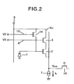
- FIG. 2 one photoelectric conversion element 1 and its peripheral circuit corresponding to a single pixel are shown in Fig. 2 .
- Fig. 2 the same elements as those shown in Fig. 1 are referred to by the same reference numerals.
- a MOS transistor forming the source follower
- V ds > V gs - V th
- V ds is the voltage difference between the drain and the source
- V gs is the voltage difference between the gate and the source
- V th is a threshold voltage.
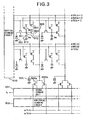
- Fig. 3 is a circuit diagram illustrating a brief configuration of a conventional CMOS area sensor.
- a two-dimensional area sensor having 2 ⁇ 2 pixels is shown, however, the number of pixels is not limited to this.
- a photodiode 901 as a transfer switch
- a MOS transistor 902 as a reset switch
- a MOS transistor 903 as an amplifier
- a MOS transistor 904 as a row selection switch
- the gate of the transfer switch 911 is connected to a line which is driven by a signal ⁇ TX(n, n+1) by a vertical scanning circuit 910
- the gate of the reset switch 902 is connected to a line which is driven by a signal ⁇ RES(n, n+1) by the vertical scanning circuit 910
- the gate of the row selection switch 904 is connected to a line which is driven by a signal ⁇ SEL(n, n+1) by the vertical scanning circuit 910.
- Photoelectric conversion is performed in each photodiode 901, and while generating the photo-charge, the transfer switch 911 is in the OFF state and the photo-charge is not transferred to the gate of the amplifier 903.
- the gate of the MOS transistor 903 is initialized to a predetermined voltage by turning on the reset switch 902 before the photo-charge is transferred.
- the predetermined voltage is a dark level.
- the row selection switch 904 is turned on, and the source follower, configured with a constant current source 905 and the amplifier (MOS transistor) 903, starts operating.
- the transfer switch 911 is turned on, thereby the charge generated by the photodiode 901 is transferred to the gate of the amplifier 903.
- outputs of the selected row are transferred to vertical output lines 906.
- the outputs are then stored in a signal storage unit 907 via MOS transistors 909a and 909b which work as transfer gates.
- the outputs, temporarily stored in the signal storage unit 907, are sequentially outputted as V 0 under control of a horizontal scanning circuit 908.
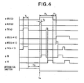
- Fig. 4 is a timing chart for operating the CMOS area sensor shown in Fig. 3 .
- signals ⁇ TX(n) and ⁇ TX(n+1) become active, and charges generated by the photodiodes 901 of all the pixels are transferred to the gates of the MOS transistors 903 via the transfer switches 911, thereby the photodiodes 901 are reset.
- a part of the charges in the cathodes of the photodiodes 901 are transferred to the gates of the MOS transistors 903 and the voltages of the cathodes and the gates become the same level.
- potential of the MOS transistor 903 becomes the same level as that of the cathode of the photodiode 901 when it is reset.
- a mechanical shutter (not shown) is open for letting in light from an object; therefore, right after the period T1 is over, a charging process starts in every pixel simultaneously.
- the mechanical shutter is kept open during a period T3, and this period is a charging period of the photodiodes 901.
- the mechanical shutter closes at time T4, thereby the charging process of the photodiodes 901 completes. In this state, photo-charges are stored in the photodiodes 901. Next, the stored photo-charges start being read by row.
- the signal ⁇ SEL(n) becomes active, thereby the row selection switches 904 in the n-th row are turned on.
- the source followers each of which includes the MOS transistor 903 of the pixel in the n-th row, become active.
- the signal ⁇ RES(n) becomes active in a period T2
- the reset switches 902 in the n-th row are turned on, thereby the gates of the MOS transistors 903 are initialized. Accordingly, signals of dark level are outputted to the vertical output lines 906.
- the signal ⁇ TN(n) becomes active, and the transfer gates 909b are turned on, and the signals of dark level are stored in the signal storage unit 907.
- the aforesaid operation is simultaneously performed for all the pixels in the n-th row.
- the signal ⁇ TX(n) becomes active, and the transfer switches 911 in the n-th row are turned on. Accordingly, the photo-charges stored in the photodiodes 901 in the n-th row are transferred to the gates of the MOS transistors 903.
- potential at the gate of each MOS transistor 903 changes from the dark level, or the reset level, by an amount of the transferred charge, and a signal of a level corresponding to the changed potential is outputted to the vertical output line 906.
- the signal ⁇ TS becomes active, the transfer gates 909a are turned on, and the signals on the vertical output lines 906 (the levels of these signals are referred to as "signal level” hereinafter) are stored in the signal storage unit 907.
- This operation is simultaneously performed for all the pixels in the n-th row.
- the signal storage unit 907 stores the dark levels and the signal levels of all the pixels in the n-th row, thus, by taking the difference between the dark level and the signal level of each pixel, fixed pattern noise caused by variation in threshold voltage Vth between the MOS transistors 903 and thermal noise (KTC noise) generated when resetting the MOS transistors 903 by the reset switches 902 are canceled. Accordingly, it is possible to obtain high S/N signals from which noise components are reduced.
- the difference signals, stored in the signal storage unit 907, between the dark levels and the signal levels are read out horizontally under control of the horizontal scanning circuit 908 during the period T7 time-serially.
- the output operation of the signals in the n-th row is completed.
- the solid state image sensing elements of the above configuration are formed in processes of forming CMOS transistors, therefore, it is possible to integrate the image sensing elements and the peripheral circuits on one chip. Accordingly, manufacturing cost is reduced and high performance is realized.
- V G (FD) max V G RES - V th RES
- V G (RES) the potential at the gate of the reset switch 902
- V th (RES) the threshold voltage of the reset switch 902.
- the maximum input level V G (FD) max is the difference between the signal level ⁇ RES(n), applied to the gate of the reset switch 902, and the threshold voltage between the gate and source of the reset switch 902.
- V G (FD) min V G TX - V th TX
- V G (TX) the potential at the gate of the transfer switch 911
- V th (TX) the threshold voltage of the transfer switch 911.
- V G (FD) min the difference between the signal level ⁇ TX(n), applied at the gate of the reset switch 911, and a threshold voltage between the gate and source of the transfer switch 911.
- the input dynamic range, Dy is, In equation (5) of the input dynamic range Dy, V th (TX) and V th (RES) of the MOS transistors differ, one from the other, since there are variations in the manufactured MOS transistors. This makes the input dynamic range Dy unstable.
- the photoelectric conversion device will be applied to devices which require a higher resolution (more pixels) and lower energy consumption (lower voltage), such as a digital still camera and a video camcorder, in the future.
- the conventional circuit can not meet the aforesaid demands of high resolution (more pixels), which causes an increase in driving load, and of low energy consumption (lower voltage), which causes deterioration of dynamic range.
- the present invention has been made in consideration of the above situation, and has as its object to provide a photoelectric conversion device having good input-output linearity as recited in claim 1.
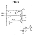
- the overall configuration of a photoelectric conversion device according to first to eighth background examples of the present invention is the same as shown in Fig. 1 .
- characteristics of the MOS transistors 3 and 14 of the present invention are different from those of conventional ones. Therefore, the MOS transistors, corresponding to the conventional MOS transistors 2, 3 and 14, are referred to by 102, 103 and 114, respectively, in the present background example.
- Fig. 6 is a circuit diagram showing one photoelectric conversion element 1 and its peripheral circuit corresponding to a single pixel according to the first background example.
- the MOS transistor 103 which acts as a row selection switch is a field effect transistor (FET).
- FET field effect transistor
- the gate voltage of the reset switch 114 when it is on be V2
- the gate voltage of the row selection switch 103 when it is on be V3
- the drain voltage of the MOS transistor 102 be V1
- a threshold voltage of the reset switch 114 be V th0
- a threshold voltage of the row selection switch 103 be Vth1
- a threshold voltage of the MOS transistor 102 be V th2 .
- the source follower is formed with the MOS transistors 102 and 103 and the constant current source 7.
- the photoelectric conversion device is designed so that a MOS transistor of the source follower always satisfies the equation (1).
- a condition of designing the source follower so as to satisfy the equation (1) is explained.
- V ds in the equation (1) V1
- V gs the gate voltage of the MOS transistor 102
- V th V th 2.
- V ⁇ 1 V c ⁇ 1 - R on ⁇ I a > V gs - V th ⁇ 2
- V out A ⁇ V in ⁇
- A a gain
- ⁇ a parameter value
- input-output linearity of the source follower is defined by how much the value of ⁇ deviates from 1.
- Fig. 16 is a graph showing improvement of the input-output linearity according to the present background example as described in the first to eighth background examples.
- the abscissa shows an ON-state impedance of the row selection switch 103, and the ordinate shows ⁇ value.
- the input-output linearity of the source follower is secured in the region where the equation (7) holds.
- V sig0 V ⁇ 2 - V th ⁇ 0
- V ⁇ 1 V ⁇ 3 - V th ⁇ 1 - I a / K 1 / 2
- the threshold voltage V th0 of the reset switch 114 and the threshold voltage V th1 of the row selection switch 103, when the reset voltage V sig0 is applied to the gate of the MOS transistor 102, are the same.
- the equation (12) is simplified to, I a / K 1 / 2 ⁇ V th ⁇ 2
- the maximum current which may flow though the source follower is limited by the threshold voltage V th2 of the MOS transistor 102, as seen from the equation (13).
- the configuration explained in the first background example can not meet the demand.
- V th0 + V th2 - V th1 is larger than V th2 of the equation (13), i.e., V th0 + V th2 - V th1 > V th2 . Therefore, it is possible to set the current I a expressed by the equation (18) to a larger value than that expressed by the equation (13).
- the threshold voltages of the MOS transistors 114, 103 and 102 may be arbitrarily determined in accordance with the utilization purpose.
- reference numeral 401 denotes a semiconductor substrate, and in Fig. 7 , it is a p type semiconductor.
- reference 402 denotes gate electrodes formed on the semiconductor substrate 401 separated by gate oxide 405, and made of, e.g., polysilicon, polycide, and a laminated film thereof.
- Reference numeral 403 denotes source electrodes and drain electrodes of the opposite conductive type to the semiconductor substrate 401, formed by, e.g., ion implantation in the semiconductor substrate 401.
- the foregoing components configure field effect transistors (FET).
- a doped layer 404 in the channel region of a desired transistor, it is possible to easily make a transistor having a threshold voltage different from other transistors. For instance, in Fig. 7 , by doping n type ion to form the doped layer 404, it is possible to decrease the threshold voltage comparing to the one which does not have a doped layer. In contrast, by doping p type ion, it is possible to increase the threshold voltage. A change in threshold voltage can be precisely determined by controlling impurity concentration and depth of the doped layer 404.
- doped layer is formed in one transistor.
- doped layers having different impurity concentrations, set to optimal conditions may be formed in more than one transistors.
- Fig. 8 As another method for changing a threshold voltage, there is a method of configuring a transistor as shown in Fig. 8 . Note, in Fig. 8 , the same portions as those shown in Fig. 7 are referred to by the same reference numerals, and explanation of them are omitted.
- reference numeral 501 denotes a well formed in a region where a desired transistor is formed.
- the impurity concentration of the p type well 501 is different from the impurity concentration of the semiconductor substrate 401 of the same p type.
- the well 501 having a different impurity concentration from that of the semiconductor substrate 401, it is possible to easily control the threshold voltage of the desired transistor. Note, in Fig.
- a case where a p type well is formed in a p type substrate however, the present invention is not limited to this, and it is possible to form a plurality of p type wells having different impurity concentrations, controlled so as to obtain desired threshold voltages, in an n type substrate.
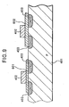
- Fig. 9 As another method for changing a threshold voltage, there is a method of configuring a transistor as shown in Fig. 9 . Note, in Fig. 9 , the same portions as those shown in Fig. 7 are referred to by the same reference numerals, and explanation of them are omitted.
- Reference numerals 601 and 602 denotes are dielectric films under gate electrodes of respective FETs.
- the dielectric films are called "gate dielectric film” hereinafter.
- the same effect is obtained by using different materials, having different dielectric constants, as the gate dielectric films in different transistors.
- silicon oxide may be used in one transistor and silicon nitride may be used in another transistor. In this way, it is possible to form a transistor having a different threshold voltage from that of the other transistor.
- Fig. 10 As another method for changing the threshold voltage, there is a method of configuring a transistor as shown in Fig. 10 . Note, in Fig. 10 , the same portions as those shown in Fig. 7 are referred to by the same reference numerals, and explanation of them are omitted.
- each FET is formed in each well 501 whose conductive type is opposite to that of the source and drain.
- the well 501 where a transistor whose threshold voltage is desired to be changed is formed, is separated at a distance from other wells for other transistors.
- the wells 501 in Fig. 10 are connected to different power supplies 701 and 702. In this configuration, by different voltages of the power supplies 701 and 702 from each other, it is possible to make the threshold voltage of a desired transistor differing from that of the other transistor due to so-called back-gate effect in a FET.
- Fig. 11 shows another method for changing the threshold voltage of a transistor. Note, in Fig. 11 , the same portions as those shown in Fig. 7 are referred to by the same reference numerals, and explanation of them are omitted.
- the lengths of gate electrodes 801 and 802 of transistors are varied.
- a phenomena that, when the gate length is less than 3 ⁇ 4 ⁇ m, the threshold voltage drops due to a fringe electric field effect at the source edge and the drain edge of a channel is known. This is called a short channel effect.
- the configuration shown in Fig. 11 utilizes the short channel effect, and by differing the gate length of a desired transistor from that of the other transistor, it is possible to realize different threshold voltages.
- transistors of single type are to be formed in a semiconductor manufacturing process; therefore, the transistors are manufactured at low cost. Further, it is unnecessary to provide extra power supply terminals as the configuration shown in Fig. 10 , a control circuit is simplified.
- Fig. 12 shows another method for changing the threshold voltage of a transistor. Note, in Fig. 12 , the same portions as those shown in Fig. 7 are referred to by the same reference numerals, and explanation of them are omitted.
- the widths of gate electrodes 803 and 804 of transistors are varied.
- a thick dielectric film is generally provided between adjacent elements for isolating each other, and the impurity concentration of the substrate under the elements is designed high so that inversion does not occur easily.
- the threshold voltage increases. This phenomenon is known as a narrow channel effect.
- the configuration shown in Fig. 12 utilizes this phenomenon, and, by differing the width of the gate electrode of a desired transistor from that of the other transistor, it is possible to realize different threshold voltages.
- transistors of single type are to be formed in a semiconductor manufacturing process; therefore, the transistors are manufactured at low cost. Further, as it is unnecessary to provide extra power supply terminals as the configuration shown in Fig. 10 , a control circuit is simplified.
- n type FET are explained as an example, however, p type FET may be used, instead of the n type FET, by controlling their threshold voltages in the similar manner.
- the third background example will be explained.
- the voltages V2 and V3, applied to the gates of the reset switch 114 and the row selection switch 103 are set to different values so as to satisfy the equation (12).
- the threshold voltage it is possible to change the threshold voltage by changing the voltage of a power supply after semiconductor manufacturing process; therefore, the threshold is controlled more precisely. Further, feed back is swiftly performed to make the threshold voltage in the optimal condition.
- the row selection switch 103 it is also possible to design the row selection switch 103 to have a different threshold voltage from the MOS transistor 102 and the reset switch 114, as described in the second background example.
- V ⁇ 1 V ⁇ 3 - V th ⁇ 1 - I a / K + V ⁇ 3 - V c ⁇ 1 - V th ⁇ 1 2 1 / 2 is obtained.
- Fig. 13 is a circuit diagram showing one photoelectric conversion element 1 and its peripheral circuit corresponding to a single pixel according to the fifth background example. Note, in Fig. 13 , the same elements as those shown in Fig. 6 are referred to by the same reference numerals, and explanation of them are omitted.
- reference numeral 1001 denotes a power supply line that is exclusively provided for the reset switch 114 and different from the power supply line for the source follower.
- a voltage V c2 is applied to the power supply line 1001.
- the reset switch 114 is designed to operate in the linear region (V c2 - V sig0 ⁇ V2 - V sig0 - V th0 ⁇ V c2 ⁇ V2 - V th0 ), and the row selection switch 103 is designed to operate in the saturation region.
- the reset voltage V sig0 is expressed by the following equation.
- V sig ⁇ 0 V c ⁇ 2
- the MOS transistor 103 it is also possible to design the MOS transistor 103 to have a different threshold voltage from those of the MOS transistors 102 and 114, as described in the second background example.
- Fig. 14 is a circuit diagram showing one photoelectric conversion element 1 and its peripheral circuit corresponding to a single pixel according to the seventh background example. Note, in Fig. 14 , the same elements as those shown in Fig. 6 are referred to by the same reference numerals, and explanation of them are omitted.
- reference numeral 1101 is a first capacitor formed between the gate of the reset switch 114 and the gate of the MOS transistor 102. As for the capacitor 1101, it may be intentionally formed, or parastic capacitance may be utilized. Reference numeral 1102 denotes a second capacitor formed between the gate of the MOS transistor 102 and ground.
- the gate voltage of the MOS transistor 102 is reset to a voltage determined on the basis of potentials of the source, gate, drain, and well of the reset switch 114.
- the reset switch 114 is turned off by changing the gate voltage of the switch 114.
- the gate voltage of the MOS transistor 102 changes by an amount which depends upon the ratio of the first capacitance 1101 to the second capacitance 1102 due to the capacitive coupling between the gate line 15 of the reset switch 114 and the gate of the MOS transistor 102.
- the reset switch 114 is an n-channel transistor, it is possible to change the potential at the gate of the MOS transistor 102 to a potential lower than the initial reset voltage.
- transistors of single type are to be formed in identical semiconductor process; therefore, the transistors are manufactured at low cost. Further, in addition to the same effect as that of the first background example, it becomes unnecessary to provide extra power supply terminals as described in a method of changing threshold voltage (4) in the second background example, by controlling substrate bias voltage.
- Fig. 15 is a circuit diagram showing one photoelectric conversion element 1 and its peripheral circuit corresponding to a single pixel according to the eighth background example of the present invention. Note, in Fig. 15 , the same elements as those shown in Fig. 6 are referred to by the same reference numerals, and explanation of them are omitted.
- reference numeral 1201 denotes a charge transfer switch for performing complete depletion transfer of signal charge from the photoelectric conversion element 1 to the gate of the MOS transistor 102.
- Reference numeral 702 denotes a transfer gate line for controlling the transfer switch 1201.
- the photoelectric conversion element 1 is designed to have large area to increase the amount of signal charge which can be stored.
- parastic capacitance on the gate of the MOS transistor 102 increases; accordingly, conversion efficiency of converting photo-charge into a voltage deteriorates, which prevents the sensitivity from improving efficiently.
- the transfer switch 1201 designing the capacitance of the gate of the MOS transistor 102 to be smaller than the capacitance of the photoelectric conversion element 1 (e.g., photodiode), and performing the complete depletion transfer, photo-charge generated by large-sized photoelectric conversion element 1 is converted to a voltage a large voltage variation inversely proportional to the capacitance of the gate of the MOS transistor 102, it is possible to improve the sensitivity.
- the transfer switch 1201 designing the capacitance of the gate of the MOS transistor 102 to be smaller than the capacitance of the photoelectric conversion element 1 (e.g., photodiode), and performing the complete depletion transfer, photo-charge generated by large-sized photoelectric conversion element 1 is converted to a voltage a large voltage variation inversely proportional to the capacitance of the gate of the MOS transistor 102, it is possible to improve the sensitivity.
- a photoelectric conversion device has a configuration shown in Fig. 3 , and explanation of it is omitted.
- the threshold voltage V th (RES) of the reset switch 902 should be set low.
- the threshold voltage V th (RES) of the reset switch 902 and the threshold voltage V th (TX) of the transfer switch 911 are set lower than the threshold voltages of the row selection switch 904 and the MOS transistor 903.
- thresholds of the transfer switches 911 of different pixels vary from each other as well as thresholds of the reset switches 902 of different pixels vary from each other due to manufacturing variation of transistors, in addition to intentionally formed difference between the threshold V th (TX) of the transfer switch 911 and the threshold V th (RES) of the reset switch 902.
- TX threshold V th
- RES threshold V th
- reference numerals 404 and 404' denote doped channel regions.
- doping is performed on a channel region of every transistor once to form the doped layer 404, and then, doping is further performed on a channel region of a desired transistor; thereby doped layers 404 and 404', having different impurity concentrations, are formed.
- doping n type ion to the doped layer 404 in the second doping process the threshold voltage is lowered compared to transistors to which second doping is not processed.
- doping p type ion it is possible to increase the threshold voltage.
- the amount of change in threshold voltage can be precisely determined by controlling the concentration of the doped layer 404' after the second doping is performed.
- the thresholds of the transfer switch 911 and the reset switch 902 are determined in a single process, an amount and direction of manufacturing variation of transistors become the same between the thresholds V th (TX) and V th (RES) of the transfer switch 911 and the reset switch 902, thus the value of the V th (TX) - V th (RES) in the equation (5) is stabilized; as a result, the input dynamic range is stabilized.
- the thresholds of the transfer switch 911 and the reset switch 902 become greater than those of the MOS transistor 903 and the row selection switch 904.
- the dynamic range is widened.
- Fig. 18 is a circuit diagram illustrating a configuration of a photoelectric conversion device according to the first embodiment. Note, in Fig. 18 , the same elements as those shown in Fig. 3 are referred to by the same reference numerals, and explanation of them are omitted.
- photo-charge stored in the photodiode 901 are provided to the gate of the MOS transistor 903 via the transfer switch 911, and as the selection pulse ⁇ SEL becomes high, the MOS transistor 903 is activated. Then, the charges are read out as the source follower is driven by the constant current source 905, and a signal corresponding to the gate voltage of the MOS transistor 903 appears on the vertical output line 906. Thereafter, when the signal ⁇ TS becomes high, charges consequently corresponding to the photo-charge generated by the photodiode 901 are stored in the signal storage unit 907.
- the gate of the MOS transistor 903 is reset to a high level by making the signal ⁇ RES high.
- the MOS transistor 903 is activated.
- a noise component is stored via the vertical output line 906 in the signal storage unit 907 by turning on the transfer gate 909b.
- V G (RES) - V th (RES) V G (SF)
- V G (RES) is the gate voltage of the reset switch 902
- V G (SF) is a reset potential at the gate of the MOS transistor 903
- V th (SF) of the MOS transistor 903 should not be set low for stabilizing its operation. Therefore, V th SF > V th RES should hold.
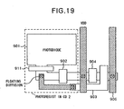
- Fig. 19 is a plan view of a single pixel of the photoelectric conversion device shown in Fig. 3 .
- the photoelectric conversion device shown in Fig. 19 includes a photodiode 901, a transfer switch 911 for transferring photo-charge generated by the photodiode 901, a MOS transistor 903 having a floating diffusion unit, a reset switch 902 for resetting the floating diffusion unit, a row selection switch 904 connected to the drain of the MOS transistor 903. Further, a power supply line VDD and a vertical output line 906 are provided.
- the transfer switch 911 and the reset switch 902 are covered with photoregist as shown by a dotted line labeled with "photoregist in CD2 (second channel doping)", then ion implantation is performed.
- the gate lengths of the transfer switch 911 and the reset switch 902 to be short and designing the gate lengths of the MOS transistor 903 and the row selection switch 904 to be long, and/or by designing the channel length of the row selection switch 904 to be longer than the channel lengths of the reset switch 902 and the MOS transistor 903, it is possible to increase the linear operation range of the photoelectric conversion device.
- Fig. 20 is a plan view showing an example of a specific arrangement of a pixel of the photoelectric conversion device shown in Fig. 19 .
- the channel length of the transfer switch 911 is 0.6 ⁇ m
- the channel length of the reset switch 902 for resetting the floating diffusion unit is 0.6 ⁇ m
- the channel length of the MOS transistor 903 is 1.0 ⁇ m
- the channel length of the selection switch 904 is 1.0 ⁇ m.
- the photoelectric conversion devices according to ninth background example and first and second embodiments can be manufactured together with shift resistors, which act as a scanning circuit, in a CMOS manufacturing process, although the devices use photodiodes; therefore, by improving the dynamic range and linearity of the photoelectric conversion devices, and reducing variation in dynamic range of the photoelectric conversion devices, it is possible to generally use the photoelectric conversion devices as so-called CMOS sensors.
Claims (12)
- Dispositif de conversion photoélectrique ayant de multiples cellules de pixels comprenant chacune un élément de conversion photoélectrique (901), un premier commutateur (911) destiné à transférer une charge générée par ledit élément de conversion photoélectrique, un transistor à effet de champ (903), ayant une zone de grille destinée à recevoir la charge transférée, destiné à délivrer en sortie un signal correspondant à la charge stockée dans la zone de grille, et un deuxième commutateur (902) destiné à remettre à l'état initial la zone de grille dudit transistor à effet de champ ;
caractérisé en ce que :la tension de seuil dudit transistor à effet de champ (903) est supérieure à la tension de seuil dudit premier commutateur (911) et est supérieure à la tension de seuil dudit second commutateur (902). - Dispositif de conversion photoélectrique selon la revendication 1, dans lequel chacune desdites cellules de pixels comprend en outre un troisième commutateur (904) connecté entre ledit transistor à effet de champ (903) et une alimentation en énergie destinée à fournir de l'énergie électrique audit transistor à effet de champ.
- Dispositif de conversion photoélectrique selon la revendication 2, dans lequel la tension de seuil dudit deuxième commutateur (902) est différente de la tension de seuil dudit troisième commutateur (904);
- Dispositif de conversion photoélectrique selon l'une quelconque des revendications 1 à 3, dans lequel ledit premier commutateur (911) et ledit deuxième commutateur (902) sont des transistors à effet de champ.
- Dispositif de conversion photoélectrique selon la revendication 4, dans lequel la concentration d'impuretés dans la région de canal dudit transistor à effet de champ, destiné à délivrer en sortie un signal, est différente de la concentration d'impuretés dans la région de canal de chacun dudit premier commutateur et dudit deuxième commutateur.
- Dispositif de conversion photoélectrique selon la revendication 5, dans lequel la tension de seuil dudit transistor à effet de champ (903) destiné à délivrer en sortie un signal, est rendue supérieure à la tension de seuil de chacun dudit premier commutateur (911) et dudit deuxième commutateur (902) en dopant d'abord toutes les régions de canal dudit transistor à effet de champ destiné à délivrer en sortie un signal, dudit premier commutateur et dudit deuxième commutateur avec un dopant d'une concentration d'impuretés prédéterminée, puis en dopant en outre une région de canal dudit transistor à effet de champ destiné à délivrer en sortie un signal.
- Dispositif de conversion photoélectrique selon la revendication 4, dans lequel la région de puits dudit transistor à effet de champ destiné à délivrer en sortie un signal, a une concentration d'impuretés différente de celle de la région de puits de chacun dudit premier commutateur et dudit deuxième commutateur.
- Dispositif de conversion photoélectrique selon la revendication 4, dans lequel le film diélectrique de grille dudit transistor à effet de champ destiné à délivrer en sortie un signal, a une épaisseur différente de l'épaisseur du film diélectrique de grille de chacun dudit premier commutateur et dudit deuxième commutateur.
- Dispositif de conversion photoélectrique selon la revendication 4, dans lequel le film diélectrique de grille dudit transistor à effet de champ destiné à délivrer en sortie un signal, est d'une matière ayant une constante diélectrique différente de la constante diélectrique du film diélectrique de grille de chacun dudit premier commutateur et dudit deuxième commutateur.
- Dispositif de conversion photoélectrique selon la revendication 4, dans lequel ledit transistor à effet de champ (903) destiné à délivrer en sortie un signal, ledit premier commutateur et ledit deuxième commutateur sont formés sur des régions de puits différentes qui sont isolées les unes des autres, ledit dispositif de conversion photoélectrique comprenant en outre un moyen à source de tension destiné à appliquer une tension, différente d'une tension appliquée aux régions de puits dudit premier commutateur et dudit deuxième commutateur, à la région de puits dudit transistor à effet de champ destiné à délivrer en sortie un signal.
- Dispositif de conversion photoélectrique selon la revendication 4, dans lequel la longueur de grille dudit transistor à effet de champ destiné à délivrer en sortie un signal, est différente de la longueur de grille de chacun dudit premier commutateur et dudit deuxième commutateur.
- Dispositif de conversion photoélectrique selon la revendication 4, dans lequel ledit transistor à effet de champ destiné à délivrer en sortie un signal a une largeur de grille différente de la largeur de grille de chacun dudit premier commutateur et dudit deuxième commutateur.
Applications Claiming Priority (5)
| Application Number | Priority Date | Filing Date | Title |
|---|---|---|---|
| JP26354597 | 1997-09-29 | ||
| JP26354597A JP3428875B2 (ja) | 1997-09-29 | 1997-09-29 | 光電変換装置 |
| JP36108997A JP3487575B2 (ja) | 1997-12-26 | 1997-12-26 | 光電変換装置 |
| JP36108997 | 1997-12-26 | ||
| EP98307838A EP0905788B1 (fr) | 1997-09-29 | 1998-09-28 | Capteur d'images de type MOS |
Related Parent Applications (1)
| Application Number | Title | Priority Date | Filing Date |
|---|---|---|---|
| EP98307838A Division EP0905788B1 (fr) | 1997-09-29 | 1998-09-28 | Capteur d'images de type MOS |
Publications (3)
| Publication Number | Publication Date |
|---|---|
| EP1592068A2 EP1592068A2 (fr) | 2005-11-02 |
| EP1592068A3 EP1592068A3 (fr) | 2006-12-27 |
| EP1592068B1 true EP1592068B1 (fr) | 2008-08-13 |
Family
ID=26546062
Family Applications (2)
| Application Number | Title | Priority Date | Filing Date |
|---|---|---|---|
| EP98307838A Expired - Lifetime EP0905788B1 (fr) | 1997-09-29 | 1998-09-28 | Capteur d'images de type MOS |
| EP05076623A Expired - Lifetime EP1592068B1 (fr) | 1997-09-29 | 1998-09-28 | Capteur d'images de type MOS |
Family Applications Before (1)
| Application Number | Title | Priority Date | Filing Date |
|---|---|---|---|
| EP98307838A Expired - Lifetime EP0905788B1 (fr) | 1997-09-29 | 1998-09-28 | Capteur d'images de type MOS |
Country Status (6)
| Country | Link |
|---|---|
| US (2) | US6670990B1 (fr) |
| EP (2) | EP0905788B1 (fr) |
| KR (1) | KR100283638B1 (fr) |
| CN (2) | CN1276514C (fr) |
| DE (2) | DE69839899D1 (fr) |
| TW (1) | TW421962B (fr) |
Families Citing this family (137)
| Publication number | Priority date | Publication date | Assignee | Title |
|---|---|---|---|---|
| JPH11103418A (ja) * | 1997-09-29 | 1999-04-13 | Canon Inc | 光電変換装置 |
| JP3466886B2 (ja) | 1997-10-06 | 2003-11-17 | キヤノン株式会社 | 固体撮像装置 |
| EP0928101A3 (fr) * | 1997-12-31 | 2001-05-02 | Texas Instruments Incorporated | Matrice de capteurs CMOS |
| JP4305970B2 (ja) * | 1998-06-05 | 2009-07-29 | ソニー株式会社 | 固体撮像素子の駆動方法 |
| JP4200545B2 (ja) * | 1998-06-08 | 2008-12-24 | ソニー株式会社 | 固体撮像素子およびその駆動方法、並びにカメラシステム |
| US6587142B1 (en) * | 1998-09-09 | 2003-07-01 | Pictos Technologies, Inc. | Low-noise active-pixel sensor for imaging arrays with high speed row reset |
| US6532040B1 (en) * | 1998-09-09 | 2003-03-11 | Pictos Technologies, Inc. | Low-noise active-pixel sensor for imaging arrays with high speed row reset |
| US6825878B1 (en) * | 1998-12-08 | 2004-11-30 | Micron Technology, Inc. | Twin P-well CMOS imager |
| US6781627B1 (en) * | 1999-06-24 | 2004-08-24 | Olympus Optical Co., Ltd. | Solid state imaging device and electric charge detecting apparatus used for the same |
| DE19933162B4 (de) * | 1999-07-20 | 2004-11-11 | Institut für Mikroelektronik Stuttgart Stiftung des öffentlichen Rechts | Bildzelle, Bildsensor und Herstellungsverfahren hierfür |
| EP1073267B1 (fr) * | 1999-07-30 | 2010-12-22 | Canon Kabushiki Kaisha | Capteur d'image de rayonnement |
| US7324144B1 (en) * | 1999-10-05 | 2008-01-29 | Canon Kabushiki Kaisha | Solid image pickup device, image pickup system and method of driving solid image pickup device |
| JP4164590B2 (ja) * | 1999-11-12 | 2008-10-15 | 本田技研工業株式会社 | 光センサ回路 |
| JP3467013B2 (ja) | 1999-12-06 | 2003-11-17 | キヤノン株式会社 | 固体撮像装置 |
| KR100429571B1 (ko) * | 1999-12-28 | 2004-05-03 | 주식회사 하이닉스반도체 | 저전력화 및 화질 개선을 위한 단위 화소 회로 및 판독 회로를 갖는 이미지센서 |
| US6965408B2 (en) * | 2000-02-28 | 2005-11-15 | Canon Kabushiki Kaisha | Solid-state image pickup device having a photoelectric conversion unit and a punch-through current suppression circuit |
| FR2807570B1 (fr) | 2000-04-07 | 2003-08-15 | Suisse Electronique Microtech | Cellule active avec memoire analogique pour un capteur photosensible realise en technologie cmos |
| SE518797C2 (sv) | 2000-07-19 | 2002-11-19 | Ericsson Telefon Ab L M | Effekt-LDMOS-transistor innefattande ett flertal parallellkopplade transistorsegment med olika tröskelspänningar |
| JP2002044523A (ja) * | 2000-07-21 | 2002-02-08 | Mitsubishi Electric Corp | 半導体撮像素子 |
| US7180798B2 (en) * | 2001-04-12 | 2007-02-20 | Fuji Electric Co., Ltd. | Semiconductor physical quantity sensing device |
| EP1301028A1 (fr) | 2001-10-05 | 2003-04-09 | STMicroelectronics Limited | Améliorations concernant les capteurs d'images CMOS |
| WO2003063247A2 (fr) * | 2002-01-24 | 2003-07-31 | Koninklijke Philips Electronics N.V. | Imageur |
| US7429764B2 (en) | 2002-02-27 | 2008-09-30 | Canon Kabushiki Kaisha | Signal processing device and image pickup apparatus using the same |
| JP3728260B2 (ja) | 2002-02-27 | 2005-12-21 | キヤノン株式会社 | 光電変換装置及び撮像装置 |
| GB0208021D0 (en) * | 2002-04-05 | 2002-05-15 | Suisse Electronique Microtech | CMOS digital image sensor |
| JP2004014911A (ja) * | 2002-06-10 | 2004-01-15 | Renesas Technology Corp | 半導体装置およびその製造方法 |
| TWI289905B (en) * | 2002-07-23 | 2007-11-11 | Fujitsu Ltd | Image sensor and image sensor module |
| US7405757B2 (en) * | 2002-07-23 | 2008-07-29 | Fujitsu Limited | Image sensor and image sensor module |
| US6744084B2 (en) * | 2002-08-29 | 2004-06-01 | Micro Technology, Inc. | Two-transistor pixel with buried reset channel and method of formation |
| KR100482370B1 (ko) * | 2002-09-27 | 2005-04-13 | 삼성전자주식회사 | 게이트 산화막의 두께가 다른 반도체장치 |
| JP4274533B2 (ja) * | 2003-07-16 | 2009-06-10 | キヤノン株式会社 | 固体撮像装置及びその駆動方法 |
| JP4514188B2 (ja) * | 2003-11-10 | 2010-07-28 | キヤノン株式会社 | 光電変換装置及び撮像装置 |
| JP4508619B2 (ja) * | 2003-12-03 | 2010-07-21 | キヤノン株式会社 | 固体撮像装置の製造方法 |
| JP3793202B2 (ja) * | 2004-02-02 | 2006-07-05 | キヤノン株式会社 | 固体撮像装置 |
| JP3890333B2 (ja) * | 2004-02-06 | 2007-03-07 | キヤノン株式会社 | 固体撮像装置 |
| JP4067054B2 (ja) * | 2004-02-13 | 2008-03-26 | キヤノン株式会社 | 固体撮像装置および撮像システム |
| US7423790B2 (en) * | 2004-03-18 | 2008-09-09 | Canon Kabushiki Kaisha | Photoelectric conversion apparatus and contact-type image sensor |
| DE602004017969D1 (de) * | 2004-06-05 | 2009-01-08 | St Microelectronics Res & Dev | Bildsensor mit geteilten Rücksetz-Signalen und Zeilenauswahl |
| US7667250B2 (en) * | 2004-07-16 | 2010-02-23 | Aptina Imaging Corporation | Vertical gate device for an image sensor and method of forming the same |
| US7087476B2 (en) * | 2004-07-28 | 2006-08-08 | Intel Corporation | Using different gate dielectrics with NMOS and PMOS transistors of a complementary metal oxide semiconductor integrated circuit |
| JP4756839B2 (ja) | 2004-09-01 | 2011-08-24 | キヤノン株式会社 | 固体撮像装置及びカメラ |
| JP4971586B2 (ja) * | 2004-09-01 | 2012-07-11 | キヤノン株式会社 | 固体撮像装置 |
| JP5089017B2 (ja) * | 2004-09-01 | 2012-12-05 | キヤノン株式会社 | 固体撮像装置及び固体撮像システム |
| JP4416668B2 (ja) | 2005-01-14 | 2010-02-17 | キヤノン株式会社 | 固体撮像装置、その制御方法及びカメラ |
| JP2006197392A (ja) * | 2005-01-14 | 2006-07-27 | Canon Inc | 固体撮像装置、カメラ、及び固体撮像装置の駆動方法 |
| JP4459064B2 (ja) * | 2005-01-14 | 2010-04-28 | キヤノン株式会社 | 固体撮像装置、その制御方法及びカメラ |
| JP4508891B2 (ja) * | 2005-01-28 | 2010-07-21 | キヤノン株式会社 | 光電変換装置、マルチチップ型イメージセンサ、密着型イメージセンサおよび画像読取装置 |
| JP4497366B2 (ja) * | 2005-02-04 | 2010-07-07 | 国立大学法人東北大学 | 光センサおよび固体撮像装置 |
| JP4452199B2 (ja) * | 2005-02-25 | 2010-04-21 | パナソニック株式会社 | 固体撮像装置およびその駆動方法 |
| JP4434991B2 (ja) * | 2005-03-01 | 2010-03-17 | キヤノン株式会社 | イメージセンサ |
| JP4459099B2 (ja) * | 2005-03-18 | 2010-04-28 | キヤノン株式会社 | 固体撮像装置及びカメラ |
| JP4677258B2 (ja) | 2005-03-18 | 2011-04-27 | キヤノン株式会社 | 固体撮像装置及びカメラ |
| JP4459098B2 (ja) * | 2005-03-18 | 2010-04-28 | キヤノン株式会社 | 固体撮像装置及びカメラ |
| JP4794877B2 (ja) * | 2005-03-18 | 2011-10-19 | キヤノン株式会社 | 固体撮像装置及びカメラ |
| KR100723485B1 (ko) * | 2005-04-11 | 2007-05-31 | 삼성전자주식회사 | 씨모스 이미지센서 및 그 제조 방법 |
| KR100871714B1 (ko) * | 2005-12-05 | 2008-12-05 | 한국전자통신연구원 | 트랜스퍼 트랜지스터 및 이를 구비한 저잡음 이미지 센서 |
| KR100673020B1 (ko) * | 2005-12-20 | 2007-01-24 | 삼성전자주식회사 | 전계효과 소오스/드레인 영역을 가지는 반도체 장치 |
| JP2007242697A (ja) * | 2006-03-06 | 2007-09-20 | Canon Inc | 撮像装置および撮像システム |
| KR101255334B1 (ko) * | 2006-05-08 | 2013-04-16 | 페어차일드코리아반도체 주식회사 | 저 열저항 파워 모듈 및 그 제조방법 |
| JP4804254B2 (ja) * | 2006-07-26 | 2011-11-02 | キヤノン株式会社 | 光電変換装置及び撮像装置 |
| JP4956084B2 (ja) * | 2006-08-01 | 2012-06-20 | キヤノン株式会社 | 光電変換装置及びそれを用いた撮像システム |
| JP4185949B2 (ja) | 2006-08-08 | 2008-11-26 | キヤノン株式会社 | 光電変換装置及び撮像装置 |
| JP5123601B2 (ja) * | 2006-08-31 | 2013-01-23 | キヤノン株式会社 | 光電変換装置 |
| JP5043388B2 (ja) * | 2006-09-07 | 2012-10-10 | キヤノン株式会社 | 固体撮像装置および撮像システム |
| JP4928199B2 (ja) * | 2006-09-07 | 2012-05-09 | キヤノン株式会社 | 信号検出装置、信号検出装置の信号読み出し方法及び信号検出装置を用いた撮像システム |
| JP5173171B2 (ja) | 2006-09-07 | 2013-03-27 | キヤノン株式会社 | 光電変換装置、撮像装置及び信号読出方法 |
| US7791010B2 (en) * | 2006-11-01 | 2010-09-07 | International Business Machines Corporation | CMOS image sensor having a third FET device with the gate terminal coupled to the diffusion region of a first FET device, the second terminal coupled to a column signal line, and the first terminal coupled to a row select signal |
| US7692130B2 (en) * | 2006-11-01 | 2010-04-06 | International Business Machines Corporation | CMOS imaging sensor having a third FET device with a gate terminal coupled to a second diffusion region of a first FET device and a first terminal coupled to a row select signal |
| JP4054839B1 (ja) | 2007-03-02 | 2008-03-05 | キヤノン株式会社 | 光電変換装置およびそれを用いた撮像システム |
| JP4101281B1 (ja) * | 2007-03-15 | 2008-06-18 | キヤノン株式会社 | 固体撮像装置及び固体撮像装置の駆動方法 |
| JP4110193B1 (ja) | 2007-05-02 | 2008-07-02 | キヤノン株式会社 | 固体撮像装置および撮像システム |
| EP2037667B1 (fr) * | 2007-09-14 | 2017-08-23 | Canon Kabushiki Kaisha | Appareil de détection d'images et système d'imagerie |
| US8063964B2 (en) * | 2007-11-20 | 2011-11-22 | Altasens, Inc. | Dual sensitivity image sensor |
| JP5004775B2 (ja) * | 2007-12-04 | 2012-08-22 | キヤノン株式会社 | 撮像装置及び撮像システム |
| JP5142696B2 (ja) | 2007-12-20 | 2013-02-13 | キヤノン株式会社 | 光電変換装置、及び光電変換装置を用いた撮像システム |
| JP5268389B2 (ja) * | 2008-02-28 | 2013-08-21 | キヤノン株式会社 | 固体撮像装置、その駆動方法及び撮像システム |
| JP5094498B2 (ja) | 2008-03-27 | 2012-12-12 | キヤノン株式会社 | 固体撮像装置及び撮像システム |
| JP5328207B2 (ja) * | 2008-04-01 | 2013-10-30 | キヤノン株式会社 | 固体撮像装置 |
| JP4500862B2 (ja) * | 2008-04-11 | 2010-07-14 | キヤノン株式会社 | 固体撮像装置の駆動方法 |
| US8026968B2 (en) * | 2008-04-11 | 2011-09-27 | Aptina Imaging Corporation | Method and apparatus providing dynamic boosted control signal for a pixel |
| FR2930841B1 (fr) * | 2008-04-30 | 2010-08-13 | E2V Semiconductors | Capteur d'image a coins coupes avec un multiplexeur entre deux lignes adjacentes de pixels. |
| JP2012090358A (ja) * | 2008-06-16 | 2012-05-10 | Norio Akamatsu | 電界効果発電装置 |
| JP5161676B2 (ja) * | 2008-07-07 | 2013-03-13 | キヤノン株式会社 | 撮像装置及び撮像システム |
| JP5283216B2 (ja) * | 2008-07-31 | 2013-09-04 | 国立大学法人静岡大学 | 高速電荷転送フォトダイオード、ロックインピクセル及び固体撮像装置 |
| JP5288955B2 (ja) * | 2008-09-09 | 2013-09-11 | キヤノン株式会社 | 固体撮像装置、撮像システム、および固体撮像装置の駆動方法 |
| JP5264379B2 (ja) * | 2008-09-12 | 2013-08-14 | キヤノン株式会社 | 撮像装置、撮像システム及び撮像装置の動作方法 |
| KR101024740B1 (ko) * | 2008-09-30 | 2011-03-24 | 주식회사 동부하이텍 | 이미지센서 및 그 제조방법 |
| JP4891308B2 (ja) * | 2008-12-17 | 2012-03-07 | キヤノン株式会社 | 固体撮像装置及び固体撮像装置を用いた撮像システム |
| JP5478905B2 (ja) * | 2009-01-30 | 2014-04-23 | キヤノン株式会社 | 固体撮像装置 |
| JP5529613B2 (ja) | 2009-04-17 | 2014-06-25 | キヤノン株式会社 | 光電変換装置及び撮像システム |
| JP5511220B2 (ja) | 2009-05-19 | 2014-06-04 | キヤノン株式会社 | 固体撮像装置 |
| US8390335B2 (en) * | 2009-06-24 | 2013-03-05 | Futurewei Technologies, Inc. | Signal buffer amplifier |
| KR101074795B1 (ko) * | 2009-07-03 | 2011-10-19 | 삼성모바일디스플레이주식회사 | 광 센싱 회로, 이를 포함하는 터치 패널, 및 광 센싱 회로의 구동 방법 |
| JP5274420B2 (ja) * | 2009-09-24 | 2013-08-28 | キヤノン株式会社 | 光電変換装置および撮像システム |
| JP5679653B2 (ja) | 2009-12-09 | 2015-03-04 | キヤノン株式会社 | 光電変換装置およびそれを用いた撮像システム |
| JP5780711B2 (ja) | 2010-04-06 | 2015-09-16 | キヤノン株式会社 | 固体撮像装置 |
| US20120002092A1 (en) * | 2010-06-30 | 2012-01-05 | Guidash Robert M | Low noise active pixel sensor |
| JP6045136B2 (ja) | 2011-01-31 | 2016-12-14 | キヤノン株式会社 | 光電変換装置 |
| KR101838894B1 (ko) * | 2011-07-08 | 2018-03-16 | 삼성전자주식회사 | 이미지 센서 및 이를 포함하는 이미지 처리 장치 |
| JP5762199B2 (ja) | 2011-07-28 | 2015-08-12 | キヤノン株式会社 | 固体撮像装置 |
| US8709883B2 (en) * | 2011-08-19 | 2014-04-29 | Freescale Semiconductor, Inc. | Implant for performance enhancement of selected transistors in an integrated circuit |
| JP5901186B2 (ja) | 2011-09-05 | 2016-04-06 | キヤノン株式会社 | 固体撮像装置及びその駆動方法 |
| JP5858695B2 (ja) | 2011-09-08 | 2016-02-10 | キヤノン株式会社 | 固体撮像装置及び固体撮像装置の駆動方法 |
| JP5801665B2 (ja) | 2011-09-15 | 2015-10-28 | キヤノン株式会社 | 固体撮像装置、a/d変換器およびその制御方法 |
| JP5806566B2 (ja) | 2011-09-15 | 2015-11-10 | キヤノン株式会社 | A/d変換器および固体撮像装置 |
| JP5907500B2 (ja) * | 2011-10-06 | 2016-04-26 | 国立研究開発法人産業技術総合研究所 | 光電変換装置、光電変換アレイおよび撮像装置 |
| JP5922905B2 (ja) | 2011-10-07 | 2016-05-24 | キヤノン株式会社 | 固体撮像装置の製造方法 |
| JP5901212B2 (ja) | 2011-10-07 | 2016-04-06 | キヤノン株式会社 | 光電変換システム |
| JP5484422B2 (ja) | 2011-10-07 | 2014-05-07 | キヤノン株式会社 | 固体撮像装置 |
| JP5930651B2 (ja) | 2011-10-07 | 2016-06-08 | キヤノン株式会社 | 固体撮像装置 |
| JP2013084744A (ja) * | 2011-10-07 | 2013-05-09 | Sony Corp | 固体撮像素子および電子機器 |
| US9093351B2 (en) * | 2012-03-21 | 2015-07-28 | Canon Kabushiki Kaisha | Solid-state imaging apparatus |
| JP6319946B2 (ja) | 2013-04-18 | 2018-05-09 | キヤノン株式会社 | 固体撮像装置及び撮像システム |
| JP6100074B2 (ja) | 2013-04-25 | 2017-03-22 | キヤノン株式会社 | 光電変換装置及び撮像システム |
| JP6274788B2 (ja) | 2013-08-28 | 2018-02-07 | キヤノン株式会社 | 撮像装置、撮像システム及び撮像装置の駆動方法 |
| JP5886806B2 (ja) | 2013-09-17 | 2016-03-16 | キヤノン株式会社 | 固体撮像装置 |
| JP6207351B2 (ja) | 2013-11-12 | 2017-10-04 | キヤノン株式会社 | 固体撮像装置および撮像システム |
| JP6239975B2 (ja) | 2013-12-27 | 2017-11-29 | キヤノン株式会社 | 固体撮像装置及びそれを用いた撮像システム |
| JP6541347B2 (ja) | 2014-03-27 | 2019-07-10 | キヤノン株式会社 | 固体撮像装置および撮像システム |
| JP6548391B2 (ja) | 2014-03-31 | 2019-07-24 | キヤノン株式会社 | 光電変換装置および撮像システム |
| JP6412328B2 (ja) | 2014-04-01 | 2018-10-24 | キヤノン株式会社 | 固体撮像装置およびカメラ |
| JP6351404B2 (ja) | 2014-07-02 | 2018-07-04 | キヤノン株式会社 | 撮像装置及び撮像システム |
| US9711558B2 (en) * | 2014-09-12 | 2017-07-18 | Panasonic Intellectual Property Management Co., Ltd. | Imaging device with photoelectric converter |
| US9979916B2 (en) | 2014-11-21 | 2018-05-22 | Canon Kabushiki Kaisha | Imaging apparatus and imaging system |
| EP3292567A4 (fr) * | 2015-05-04 | 2019-02-27 | Thin Film Electronics ASA | Circuits à base moscap pour dispositifs de communication électroniques et procédés de fabrication et d'utilisation associés |
| US9900539B2 (en) | 2015-09-10 | 2018-02-20 | Canon Kabushiki Kaisha | Solid-state image pickup element, and image pickup system |
| US9716155B2 (en) | 2015-12-09 | 2017-07-25 | International Business Machines Corporation | Vertical field-effect-transistors having multiple threshold voltages |
| KR101679598B1 (ko) * | 2016-01-04 | 2016-11-25 | 주식회사 동부하이텍 | 이미지 센서 |
| JP6740067B2 (ja) | 2016-09-16 | 2020-08-12 | キヤノン株式会社 | 固体撮像装置及びその駆動方法 |
| JP6750876B2 (ja) | 2016-10-07 | 2020-09-02 | キヤノン株式会社 | 固体撮像装置及びその駆動方法 |
| JP2018082261A (ja) | 2016-11-15 | 2018-05-24 | キヤノン株式会社 | 撮像素子 |
| JP6806553B2 (ja) | 2016-12-15 | 2021-01-06 | キヤノン株式会社 | 撮像装置、撮像装置の駆動方法及び撮像システム |
| JP6871797B2 (ja) | 2017-04-24 | 2021-05-12 | キヤノン株式会社 | 光電変換装置 |
| JP7299680B2 (ja) | 2018-08-23 | 2023-06-28 | キヤノン株式会社 | 撮像装置及び撮像システム |
| US11425365B2 (en) | 2018-12-14 | 2022-08-23 | Canon Kabushiki Kaisha | Photoelectric conversion device, method of manufacturing photoelectric conversion device, and method of manufacturing semiconductor device |
| CN112580399A (zh) * | 2019-09-29 | 2021-03-30 | 京东方科技集团股份有限公司 | 一种指纹识别电路及其驱动方法、显示面板、显示装置 |
| WO2022126395A1 (fr) * | 2020-12-15 | 2022-06-23 | 深圳市大疆创新科技有限公司 | Capteur d'image et son procédé de commande, processeur d'image et dispositif d'imagerie |
Family Cites Families (22)
| Publication number | Priority date | Publication date | Assignee | Title |
|---|---|---|---|---|
| JPH0760888B2 (ja) | 1985-06-12 | 1995-06-28 | キヤノン株式会社 | 光電変換装置 |
| JPH0654957B2 (ja) | 1985-11-13 | 1994-07-20 | キヤノン株式会社 | 光電変換装置 |
| JPH0644619B2 (ja) | 1986-07-17 | 1994-06-08 | キヤノン株式会社 | 光電変換装置 |
| JPS63100879A (ja) * | 1986-10-17 | 1988-05-02 | Hitachi Ltd | 固体撮像装置 |
| US4866293A (en) | 1986-12-09 | 1989-09-12 | Canon Kabushiki Kaisha | Photoelectric converting apparatus to prevent the outflow of excess carriers |
| DE3856165T2 (de) | 1987-01-29 | 1998-08-27 | Canon Kk | Photovoltaischer Wandler |
| JPH01292856A (ja) | 1988-05-20 | 1989-11-27 | Hitachi Ltd | 固体撮像装置 |
| US6127692A (en) | 1989-08-04 | 2000-10-03 | Canon Kabushiki Kaisha | Photoelectric conversion apparatus |
| CA2056087C (fr) | 1990-11-27 | 1998-01-27 | Masakazu Morishita | Dispositif de conversion photo-electrique et appareil de traitement d'informations utilisant ce dispositif |
| JP2913876B2 (ja) * | 1991-03-08 | 1999-06-28 | ソニー株式会社 | 固体撮像装置 |
| US5453611A (en) | 1993-01-01 | 1995-09-26 | Canon Kabushiki Kaisha | Solid-state image pickup device with a plurality of photoelectric conversion elements on a common semiconductor chip |
| JPH06334920A (ja) | 1993-03-23 | 1994-12-02 | Nippon Hoso Kyokai <Nhk> | 固体撮像素子とその駆動方法 |
| JPH09511361A (ja) * | 1994-02-11 | 1997-11-11 | リットン システムズ カナダ リミテッド | デュアルゲート薄膜トランジスタを用いた電磁放射線画像装置 |
| JPH08186241A (ja) | 1995-01-06 | 1996-07-16 | Canon Inc | 撮像素子と固体撮像装置 |
| US5654537A (en) * | 1995-06-30 | 1997-08-05 | Symbios Logic Inc. | Image sensor array with picture element sensor testability |
| WO1997007630A1 (fr) * | 1995-08-11 | 1997-02-27 | Kabushiki Kaisha Toshiba | Dispositif mos de prise d'image |
| JP3559640B2 (ja) * | 1996-02-27 | 2004-09-02 | キヤノン株式会社 | 光電変換装置 |
| US5869857A (en) * | 1997-04-07 | 1999-02-09 | Chen; Pao-Jung | CMOS photodetectors with wide range operating region |
| US6043525A (en) * | 1997-04-07 | 2000-03-28 | Chen; Pao-Jung | High speed CMOS photodetectors with wide range operating region |
| JP3673620B2 (ja) * | 1997-07-18 | 2005-07-20 | キヤノン株式会社 | 光電変換装置 |
| EP0928101A3 (fr) | 1997-12-31 | 2001-05-02 | Texas Instruments Incorporated | Matrice de capteurs CMOS |
| US6414292B1 (en) * | 1999-10-29 | 2002-07-02 | Intel Corporation | Image sensor with increased pixel density |
-
1998
- 1998-09-21 TW TW087115716A patent/TW421962B/zh active
- 1998-09-28 DE DE69839899T patent/DE69839899D1/de not_active Expired - Lifetime
- 1998-09-28 DE DE69836608T patent/DE69836608T2/de not_active Expired - Lifetime
- 1998-09-28 EP EP98307838A patent/EP0905788B1/fr not_active Expired - Lifetime
- 1998-09-28 EP EP05076623A patent/EP1592068B1/fr not_active Expired - Lifetime
- 1998-09-28 US US09/161,402 patent/US6670990B1/en not_active Expired - Lifetime
- 1998-09-29 KR KR1019980040647A patent/KR100283638B1/ko not_active IP Right Cessation
- 1998-09-29 CN CNB2003101186230A patent/CN1276514C/zh not_active Expired - Fee Related
- 1998-09-29 CN CNB98120788XA patent/CN1155207C/zh not_active Expired - Fee Related
-
2003
- 2003-10-08 US US10/680,181 patent/US6946637B2/en not_active Expired - Fee Related
Also Published As
| Publication number | Publication date |
|---|---|
| CN1155207C (zh) | 2004-06-23 |
| EP1592068A3 (fr) | 2006-12-27 |
| KR19990030274A (ko) | 1999-04-26 |
| CN1527392A (zh) | 2004-09-08 |
| TW421962B (en) | 2001-02-11 |
| US20040065808A1 (en) | 2004-04-08 |
| DE69836608D1 (de) | 2007-01-25 |
| EP0905788B1 (fr) | 2006-12-13 |
| KR100283638B1 (ko) | 2001-04-02 |
| US6670990B1 (en) | 2003-12-30 |
| CN1213931A (zh) | 1999-04-14 |
| DE69839899D1 (de) | 2008-09-25 |
| EP0905788A3 (fr) | 2000-06-28 |
| CN1276514C (zh) | 2006-09-20 |
| US6946637B2 (en) | 2005-09-20 |
| EP1592068A2 (fr) | 2005-11-02 |
| DE69836608T2 (de) | 2007-09-27 |
| EP0905788A2 (fr) | 1999-03-31 |
Similar Documents
| Publication | Publication Date | Title |
|---|---|---|
| EP1592068B1 (fr) | Capteur d'images de type MOS | |
| US6512544B1 (en) | Storage pixel sensor and array with compression | |
| US6975356B1 (en) | Solid-state imaging device with the elimination of thermal noise | |
| US7110030B1 (en) | Solid state image pickup apparatus | |
| US9602750B2 (en) | Image sensor pixels having built-in variable gain feedback amplifier circuitry | |
| US7446807B2 (en) | Imager pixel with capacitance for boosting reset voltage | |
| US5856686A (en) | Amplifying type solid-state imaging apparatus and method for driving the same | |
| US9654713B2 (en) | Image sensors, methods, and pixels with tri-level biased transfer gates | |
| US9083901B2 (en) | Solid-state image pickup device and method of resetting the same | |
| US7692702B2 (en) | Solid-state imaging device with amplifiers corresponding to signal lines and alternating control voltage | |
| KR100760903B1 (ko) | 증폭형 고체 촬상 장치 | |
| US6697114B1 (en) | Triple slope pixel sensor and arry | |
| KR101031982B1 (ko) | 고상 촬상 디바이스 및 그 구동 방법 | |
| US20120056080A1 (en) | High Dynamic Range CMOS Pixel and Method of Operating Same | |
| US20050167707A1 (en) | Solid state image sensing device and manufacturing and driving methods thereof | |
| WO1992021151A2 (fr) | IMAGEUR A CCDs PERISTALTIQUES A GRANDE VITESSE, AVEC SORTIE DE TRANSISTOR A EFFET DE CHAMP GaAs | |
| US20040206991A1 (en) | Solid-state imaging device | |
| EP1223746B1 (fr) | Capteur d'images à pixel actif présentant une linéarité améliorée | |
| JP3833027B2 (ja) | 固体撮像装置及び画像入力装置 | |
| JP3624042B2 (ja) | 光電変換装置 | |
| JP3597176B2 (ja) | Ccd型固体撮像素子 | |
| JPH11196331A (ja) | 光電変換装置 | |
| US20230215885A1 (en) | Adjustable well capacity pixel for semiconductor imaging sensors | |
| JP3585898B2 (ja) | Ccd型固体撮像素子を用いたカメラ | |
| KR20020027021A (ko) | 씨모스 이미지 센서 |
Legal Events
| Date | Code | Title | Description |
|---|---|---|---|
| PUAI | Public reference made under article 153(3) epc to a published international application that has entered the european phase |
Free format text: ORIGINAL CODE: 0009012 |
|
| AC | Divisional application: reference to earlier application |
Ref document number: 0905788 Country of ref document: EP Kind code of ref document: P |
|
| AK | Designated contracting states |
Kind code of ref document: A2 Designated state(s): DE FR GB IT NL |
|
| PUAL | Search report despatched |
Free format text: ORIGINAL CODE: 0009013 |
|
| AK | Designated contracting states |
Kind code of ref document: A3 Designated state(s): DE FR GB IT NL |
|
| 17P | Request for examination filed |
Effective date: 20070627 |
|
| AKX | Designation fees paid |
Designated state(s): DE FR GB IT NL |
|
| GRAP | Despatch of communication of intention to grant a patent |
Free format text: ORIGINAL CODE: EPIDOSNIGR1 |
|
| GRAS | Grant fee paid |
Free format text: ORIGINAL CODE: EPIDOSNIGR3 |
|
| GRAA | (expected) grant |
Free format text: ORIGINAL CODE: 0009210 |
|
| AC | Divisional application: reference to earlier application |
Ref document number: 0905788 Country of ref document: EP Kind code of ref document: P |
|
| AK | Designated contracting states |
Kind code of ref document: B1 Designated state(s): DE FR GB IT NL |
|
| REG | Reference to a national code |
Ref country code: GB Ref legal event code: FG4D |
|
| REF | Corresponds to: |
Ref document number: 69839899 Country of ref document: DE Date of ref document: 20080925 Kind code of ref document: P |
|
| PG25 | Lapsed in a contracting state [announced via postgrant information from national office to epo] |
Ref country code: NL Free format text: LAPSE BECAUSE OF FAILURE TO SUBMIT A TRANSLATION OF THE DESCRIPTION OR TO PAY THE FEE WITHIN THE PRESCRIBED TIME-LIMIT Effective date: 20080813 |
|
| PLBE | No opposition filed within time limit |
Free format text: ORIGINAL CODE: 0009261 |
|
| STAA | Information on the status of an ep patent application or granted ep patent |
Free format text: STATUS: NO OPPOSITION FILED WITHIN TIME LIMIT |
|
| 26N | No opposition filed |
Effective date: 20090514 |
|
| PG25 | Lapsed in a contracting state [announced via postgrant information from national office to epo] |
Ref country code: IT Free format text: LAPSE BECAUSE OF FAILURE TO SUBMIT A TRANSLATION OF THE DESCRIPTION OR TO PAY THE FEE WITHIN THE PRESCRIBED TIME-LIMIT Effective date: 20080813 |
|
| PGFP | Annual fee paid to national office [announced via postgrant information from national office to epo] |
Ref country code: GB Payment date: 20090923 Year of fee payment: 12 |
|
| PGFP | Annual fee paid to national office [announced via postgrant information from national office to epo] |
Ref country code: DE Payment date: 20090930 Year of fee payment: 12 |
|
| GBPC | Gb: european patent ceased through non-payment of renewal fee |
Effective date: 20100928 |
|
| REG | Reference to a national code |
Ref country code: FR Ref legal event code: ST Effective date: 20110531 |
|
| REG | Reference to a national code |
Ref country code: DE Ref legal event code: R119 Ref document number: 69839899 Country of ref document: DE Effective date: 20110401 |
|
| PG25 | Lapsed in a contracting state [announced via postgrant information from national office to epo] |
Ref country code: FR Free format text: LAPSE BECAUSE OF NON-PAYMENT OF DUE FEES Effective date: 20100930 Ref country code: DE Free format text: LAPSE BECAUSE OF NON-PAYMENT OF DUE FEES Effective date: 20110401 |
|
| PG25 | Lapsed in a contracting state [announced via postgrant information from national office to epo] |
Ref country code: GB Free format text: LAPSE BECAUSE OF NON-PAYMENT OF DUE FEES Effective date: 20100928 |
|
| PGFP | Annual fee paid to national office [announced via postgrant information from national office to epo] |
Ref country code: FR Payment date: 20091006 Year of fee payment: 12 |