JP5922905B2 - 固体撮像装置の製造方法 - Google Patents
固体撮像装置の製造方法 Download PDFInfo
- Publication number
- JP5922905B2 JP5922905B2 JP2011223457A JP2011223457A JP5922905B2 JP 5922905 B2 JP5922905 B2 JP 5922905B2 JP 2011223457 A JP2011223457 A JP 2011223457A JP 2011223457 A JP2011223457 A JP 2011223457A JP 5922905 B2 JP5922905 B2 JP 5922905B2
- Authority
- JP
- Japan
- Prior art keywords
- region
- semiconductor substrate
- ions
- imaging device
- solid
- Prior art date
- Legal status (The legal status is an assumption and is not a legal conclusion. Google has not performed a legal analysis and makes no representation as to the accuracy of the status listed.)
- Active
Links
- 238000003384 imaging method Methods 0.000 title claims description 49
- 238000004519 manufacturing process Methods 0.000 title claims description 33
- 238000000034 method Methods 0.000 title claims description 26
- 150000002500 ions Chemical class 0.000 claims description 100
- 239000004065 semiconductor Substances 0.000 claims description 93
- 239000000758 substrate Substances 0.000 claims description 78
- 238000009825 accumulation Methods 0.000 claims description 27
- 238000006243 chemical reaction Methods 0.000 claims description 26
- 238000003860 storage Methods 0.000 claims description 22
- 238000009792 diffusion process Methods 0.000 claims description 21
- 239000012535 impurity Substances 0.000 claims description 19
- 238000002955 isolation Methods 0.000 claims description 13
- 238000000926 separation method Methods 0.000 claims description 11
- 230000001678 irradiating effect Effects 0.000 claims description 3
- 238000002347 injection Methods 0.000 claims 4
- 239000007924 injection Substances 0.000 claims 4
- 239000007787 solid Substances 0.000 claims 1
- 238000005468 ion implantation Methods 0.000 description 18
- 230000008569 process Effects 0.000 description 9
- 238000002513 implantation Methods 0.000 description 5
- 230000004048 modification Effects 0.000 description 4
- 238000012986 modification Methods 0.000 description 4
- 230000006870 function Effects 0.000 description 3
- ZOXJGFHDIHLPTG-UHFFFAOYSA-N Boron Chemical compound [B] ZOXJGFHDIHLPTG-UHFFFAOYSA-N 0.000 description 2
- 229910052796 boron Inorganic materials 0.000 description 2
- 230000008859 change Effects 0.000 description 2
- 238000010586 diagram Methods 0.000 description 2
- OAICVXFJPJFONN-UHFFFAOYSA-N Phosphorus Chemical compound [P] OAICVXFJPJFONN-UHFFFAOYSA-N 0.000 description 1
- XUIMIQQOPSSXEZ-UHFFFAOYSA-N Silicon Chemical compound [Si] XUIMIQQOPSSXEZ-UHFFFAOYSA-N 0.000 description 1
- 230000001133 acceleration Effects 0.000 description 1
- 229910052785 arsenic Inorganic materials 0.000 description 1
- RQNWIZPPADIBDY-UHFFFAOYSA-N arsenic atom Chemical compound [As] RQNWIZPPADIBDY-UHFFFAOYSA-N 0.000 description 1
- -1 boron are implanted Chemical class 0.000 description 1
- 239000002019 doping agent Substances 0.000 description 1
- 238000010438 heat treatment Methods 0.000 description 1
- 239000007943 implant Substances 0.000 description 1
- 229910052738 indium Inorganic materials 0.000 description 1
- APFVFJFRJDLVQX-UHFFFAOYSA-N indium atom Chemical compound [In] APFVFJFRJDLVQX-UHFFFAOYSA-N 0.000 description 1
- 230000007246 mechanism Effects 0.000 description 1
- 229910052698 phosphorus Inorganic materials 0.000 description 1
- 239000011574 phosphorus Substances 0.000 description 1
- 238000000206 photolithography Methods 0.000 description 1
- 238000005036 potential barrier Methods 0.000 description 1
- 229910052710 silicon Inorganic materials 0.000 description 1
- 239000010703 silicon Substances 0.000 description 1
Images


Classifications
-
- H—ELECTRICITY
- H01—ELECTRIC ELEMENTS
- H01L—SEMICONDUCTOR DEVICES NOT COVERED BY CLASS H10
- H01L27/00—Devices consisting of a plurality of semiconductor or other solid-state components formed in or on a common substrate
- H01L27/14—Devices consisting of a plurality of semiconductor or other solid-state components formed in or on a common substrate including semiconductor components sensitive to infrared radiation, light, electromagnetic radiation of shorter wavelength or corpuscular radiation and specially adapted either for the conversion of the energy of such radiation into electrical energy or for the control of electrical energy by such radiation
- H01L27/144—Devices controlled by radiation
- H01L27/146—Imager structures
- H01L27/14683—Processes or apparatus peculiar to the manufacture or treatment of these devices or parts thereof
- H01L27/14689—MOS based technologies
-
- H—ELECTRICITY
- H01—ELECTRIC ELEMENTS
- H01L—SEMICONDUCTOR DEVICES NOT COVERED BY CLASS H10
- H01L27/00—Devices consisting of a plurality of semiconductor or other solid-state components formed in or on a common substrate
- H01L27/14—Devices consisting of a plurality of semiconductor or other solid-state components formed in or on a common substrate including semiconductor components sensitive to infrared radiation, light, electromagnetic radiation of shorter wavelength or corpuscular radiation and specially adapted either for the conversion of the energy of such radiation into electrical energy or for the control of electrical energy by such radiation
- H01L27/144—Devices controlled by radiation
- H01L27/146—Imager structures
- H01L27/14643—Photodiode arrays; MOS imagers
Description
本発明の半導体装置の製造方法によれば、少なくとも2つの領域を露出させる開口を有するレジストパターンを用い、異なる方向に沿って少なくとも2回のイオンを注入する工程を実施することで、2つの領域の半導体領域を作り分けることができる。
Claims (9)
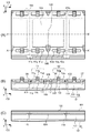
- 電荷を蓄積する蓄積領域をそれぞれが含む複数の光電変換素子と、1つ以上のMOSトランジスタとが半導体基板に形成され、前記半導体基板のうち互いに隣接する前記蓄積領域の間に分離領域を有する固体撮像装置の製造方法であって、
開口と遮蔽部とを有するレジストパターンを前記半導体基板の上に形成する形成工程と、
前記レジストパターンの前記開口を通じて前記半導体基板にイオンを注入する注入工程と
を有し、
前記形成工程で形成される前記レジストパターンは、
前記半導体基板を第1方向から見た場合に、前記分離領域を前記開口から露出し、
前記半導体基板を前記第1方向とは異なる方向から見た場合に、前記1つ以上のMOSトランジスタが形成される領域を前記開口から露出するとともに、前記分離領域を前記遮蔽部により遮り、
前記注入工程では、
前記第1方向に沿って照射されたイオンが前記分離領域に注入され、
前記異なる方向に沿って照射されたイオンが前記1つ以上のMOSトランジスタが形成される領域に注入され、
前記分離領域に注入されたイオンが、前記1つ以上のMOSトランジスタが形成される領域に注入されたイオンよりも、前記半導体基板の表面からの位置が深くなるようにイオンを照射する
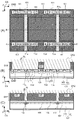
ことを特徴とする固体撮像装置の製造方法。 - 前記第1方向に沿って照射されたイオンによって、前記分離領域に不純物拡散層が形成され、前記異なる方向に沿って照射されたイオンによって、前記1つ以上のMOSトランジスタのチャネル領域にイオン導入層が形成されることを特徴とする請求項1に記載の固体撮像装置の製造方法。
- 前記異なる方向は前記第1方向よりも前記半導体基板の表面の法線に対する角度が大きいことを特徴とする請求項1又は2に記載の固体撮像装置の製造方法。
- 前記蓄積領域は第1導電型であり、前記第1方向に沿って照射されたイオンは、第2導電型の半導体領域を形成するためのイオンであることを特徴とする請求項1乃至3の何れか1項に記載の固体撮像装置の製造方法。
- 前記蓄積領域は第1導電型であり、前記異なる方向に沿って照射されたイオンは、第1導電型の半導体領域を形成するためのイオンであることを特徴とする請求項1乃至4の何れか1項に記載の固体撮像装置の製造方法。
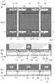
- 前記1つ以上のMOSトランジスタは第1MOSトランジスタと第2MOSトランジスタとを含み、
前記異なる方向は互いに異なる第2方向及び第3方向を含み、
前記形成工程で形成される前記レジストパターンは、
前記半導体基板を前記第2方向から見た場合に、前記第1MOSトランジスタが形成される領域を前記開口から露出し、
前記半導体基板を前記第3方向から見た場合に、前記第2MOSトランジスタが形成される領域を前記開口から露出するとともに、前記第1MOSトランジスタが形成される領域を前記遮蔽部により遮り、
前記注入工程では、
前記第2方向に沿って照射されたイオンが前記第1MOSトランジスタが形成される領域に注入され
前記第3方向に沿って照射されたイオンが前記第2MOSトランジスタが形成される領域に注入される
ことを特徴とする請求項1乃至5の何れか1項に記載の固体撮像装置の製造方法。 - 前記形成工程で形成される前記レジストパターンは、前記半導体基板を前記第2方向から見た場合に、前記第2MOSトランジスタが形成される領域を前記遮蔽部により遮ることを特徴とする請求項6に記載の固体撮像装置の製造方法。
- 前記形成工程で形成される前記レジストパターンは、
前記半導体基板を前記第1方向から見た場合に、前記蓄積領域が形成される領域の中央部分を前記開口から露出し、
前記半導体基板を前記異なる方向から見た場合に、前記中央部分を前記遮蔽部により遮り、
前記注入工程では、
前記第1方向に沿って照射されたイオンが前記中央部分に注入される
ことを特徴とする請求項1乃至7の何れか1項に記載の固体撮像装置の製造方法。 - 電荷を蓄積する蓄積領域をそれぞれが含む複数の光電変換素子と、MOSトランジスタとが半導体基板に形成された固体撮像装置の製造方法であって、
前記MOSトランジスタが形成される領域を含む第1領域と、前記第1領域と異なる領域で、隣接する前記蓄積領域の間に位置する分離領域を含む第2領域と、を露出させる開口を有するレジストパターンを前記半導体基板の上に形成する形成工程と、
前記レジストパターンの前記開口を通じて前記半導体基板にイオンを注入する注入工程と、を有し、
前記注入工程は、
第1の角度で、少なくとも前記第2領域にイオンを注入する工程と、
前記第1の角度とは異なる第2の角度で、前記第1領域のみにイオンを注入する工程と、
を有し、
前記第1の角度で前記第2領域に注入されたイオンが、前記第2の角度で前記第1領域に注入されたイオンよりも、前記半導体基板の表面からの位置が深くなるようにイオンを照射する
ことを特徴とする固体撮像装置の製造方法。
Priority Applications (2)
| Application Number | Priority Date | Filing Date | Title |
|---|---|---|---|
| JP2011223457A JP5922905B2 (ja) | 2011-10-07 | 2011-10-07 | 固体撮像装置の製造方法 |
| US13/607,107 US8835269B2 (en) | 2011-10-07 | 2012-09-07 | Method of manufacturing solid-state image sensor |
Applications Claiming Priority (1)
| Application Number | Priority Date | Filing Date | Title |
|---|---|---|---|
| JP2011223457A JP5922905B2 (ja) | 2011-10-07 | 2011-10-07 | 固体撮像装置の製造方法 |
Publications (3)
| Publication Number | Publication Date |
|---|---|
| JP2013084754A JP2013084754A (ja) | 2013-05-09 |
| JP2013084754A5 JP2013084754A5 (ja) | 2014-11-20 |
| JP5922905B2 true JP5922905B2 (ja) | 2016-05-24 |
Family
ID=48042336
Family Applications (1)
| Application Number | Title | Priority Date | Filing Date |
|---|---|---|---|
| JP2011223457A Active JP5922905B2 (ja) | 2011-10-07 | 2011-10-07 | 固体撮像装置の製造方法 |
Country Status (2)
| Country | Link |
|---|---|
| US (1) | US8835269B2 (ja) |
| JP (1) | JP5922905B2 (ja) |
Families Citing this family (2)
| Publication number | Priority date | Publication date | Assignee | Title |
|---|---|---|---|---|
| US9000500B2 (en) * | 2009-12-30 | 2015-04-07 | Omnivision Technologies, Inc. | Image sensor with doped transfer gate |
| JP2016058635A (ja) * | 2014-09-11 | 2016-04-21 | ルネサスエレクトロニクス株式会社 | 半導体装置の製造方法 |
Family Cites Families (8)
| Publication number | Priority date | Publication date | Assignee | Title |
|---|---|---|---|---|
| TW421962B (en) | 1997-09-29 | 2001-02-11 | Canon Kk | Image sensing device using mos type image sensing elements |
| JP3487575B2 (ja) | 1997-12-26 | 2004-01-19 | キヤノン株式会社 | 光電変換装置 |
| JP2000021995A (ja) * | 1998-06-26 | 2000-01-21 | Hitachi Ltd | 半導体集積回路装置の製造方法 |
| US6743652B2 (en) * | 2002-02-01 | 2004-06-01 | Stmicroelectronics, Inc. | Method for making an integrated circuit device including photodiodes |
| JP2004079813A (ja) * | 2002-08-19 | 2004-03-11 | Matsushita Electric Ind Co Ltd | 半導体装置の製造方法 |
| JP2005093866A (ja) * | 2003-09-19 | 2005-04-07 | Fuji Film Microdevices Co Ltd | 固体撮像素子の製造方法 |
| JP2007299938A (ja) | 2006-04-28 | 2007-11-15 | Sharp Corp | 固体撮像装置およびその製造方法、電子情報機器 |
| JP2008060380A (ja) | 2006-08-31 | 2008-03-13 | Matsushita Electric Ind Co Ltd | 固体撮像素子及びその製造方法 |
-
2011
- 2011-10-07 JP JP2011223457A patent/JP5922905B2/ja active Active
-
2012
- 2012-09-07 US US13/607,107 patent/US8835269B2/en active Active
Also Published As
| Publication number | Publication date |
|---|---|
| US8835269B2 (en) | 2014-09-16 |
| JP2013084754A (ja) | 2013-05-09 |
| US20130089945A1 (en) | 2013-04-11 |
Similar Documents
| Publication | Publication Date | Title |
|---|---|---|
| JP5539104B2 (ja) | 光電変換装置およびそれを用いた撮像システム | |
| US7592579B2 (en) | Photoelectric conversion device manufacturing method, semiconductor device manufacturing method, photoelectric conversion device, and image sensing system | |
| US9768213B2 (en) | Solid-state image sensor and camera | |
| JP5539029B2 (ja) | 固体撮像装置の製造方法 | |
| US9711558B2 (en) | Imaging device with photoelectric converter | |
| US10121816B2 (en) | Imaging device and method of manufacturing imaging device | |
| KR101390518B1 (ko) | 고체 촬상 장치 | |
| JP2009158932A (ja) | イメージセンサ及びその製造方法 | |
| JP2007110162A (ja) | ピン止め光ダイオードと集積されたアクティブ画素センサー | |
| JP6246076B2 (ja) | 半導体装置の製造方法および半導体装置 | |
| JP5539373B2 (ja) | 固体撮像装置及びその製造方法 | |
| US7755150B2 (en) | MOS solid-state image pickup device and manufacturing method thereof | |
| US8383497B2 (en) | Method for manufacturing solid-state image sensor | |
| WO2006130545A2 (en) | Cmos active pixel sensor shared amplifier pixel | |
| JP5922905B2 (ja) | 固体撮像装置の製造方法 | |
| KR101442358B1 (ko) | 고체 촬상 장치 및 그 제조 방법 | |
| JP2017054966A (ja) | 半導体装置の製造方法および半導体装置 | |
| US10483302B2 (en) | Solid-state imaging device | |
| US9231021B2 (en) | Image pickup apparatus, image pickup system, and image pickup apparatus manufacturing method | |
| JP2016058635A (ja) | 半導体装置の製造方法 | |
| JP2016225597A (ja) | 固体撮像装置及びカメラ | |
| JP2020057689A (ja) | 固体撮像装置及びその製造方法 | |
| JP2005109439A (ja) | 固体撮像装置及びその製造方法 | |
| JP2021190614A (ja) | 光電変換装置及びその製造方法 | |
| JP2014146804A (ja) | 光電変換装置及び撮像システム |
Legal Events
| Date | Code | Title | Description |
|---|---|---|---|
| A521 | Written amendment |
Free format text: JAPANESE INTERMEDIATE CODE: A523 Effective date: 20141007 |
|
| A621 | Written request for application examination |
Free format text: JAPANESE INTERMEDIATE CODE: A621 Effective date: 20141007 |
|
| A977 | Report on retrieval |
Free format text: JAPANESE INTERMEDIATE CODE: A971007 Effective date: 20150618 |
|
| A131 | Notification of reasons for refusal |
Free format text: JAPANESE INTERMEDIATE CODE: A131 Effective date: 20150703 |
|
| A521 | Written amendment |
Free format text: JAPANESE INTERMEDIATE CODE: A523 Effective date: 20150806 |
|
| TRDD | Decision of grant or rejection written | ||
| A01 | Written decision to grant a patent or to grant a registration (utility model) |
Free format text: JAPANESE INTERMEDIATE CODE: A01 Effective date: 20160318 |
|
| A61 | First payment of annual fees (during grant procedure) |
Free format text: JAPANESE INTERMEDIATE CODE: A61 Effective date: 20160415 |
|
| R151 | Written notification of patent or utility model registration |
Ref document number: 5922905 Country of ref document: JP Free format text: JAPANESE INTERMEDIATE CODE: R151 |