JP5922905B2 - Method for manufacturing solid-state imaging device - Google Patents
Method for manufacturing solid-state imaging device Download PDFInfo
- Publication number
- JP5922905B2 JP5922905B2 JP2011223457A JP2011223457A JP5922905B2 JP 5922905 B2 JP5922905 B2 JP 5922905B2 JP 2011223457 A JP2011223457 A JP 2011223457A JP 2011223457 A JP2011223457 A JP 2011223457A JP 5922905 B2 JP5922905 B2 JP 5922905B2
- Authority
- JP
- Japan
- Prior art keywords
- region
- semiconductor substrate
- ions
- imaging device
- solid
- Prior art date
- Legal status (The legal status is an assumption and is not a legal conclusion. Google has not performed a legal analysis and makes no representation as to the accuracy of the status listed.)
- Active
Links
- 238000003384 imaging method Methods 0.000 title claims description 49
- 238000004519 manufacturing process Methods 0.000 title claims description 33
- 238000000034 method Methods 0.000 title claims description 26
- 150000002500 ions Chemical class 0.000 claims description 100
- 239000004065 semiconductor Substances 0.000 claims description 93
- 239000000758 substrate Substances 0.000 claims description 78
- 238000009825 accumulation Methods 0.000 claims description 27
- 238000006243 chemical reaction Methods 0.000 claims description 26
- 238000003860 storage Methods 0.000 claims description 22
- 238000009792 diffusion process Methods 0.000 claims description 21
- 239000012535 impurity Substances 0.000 claims description 19
- 238000002955 isolation Methods 0.000 claims description 13
- 238000000926 separation method Methods 0.000 claims description 11
- 230000001678 irradiating effect Effects 0.000 claims description 3
- 238000002347 injection Methods 0.000 claims 4
- 239000007924 injection Substances 0.000 claims 4
- 239000007787 solid Substances 0.000 claims 1
- 238000005468 ion implantation Methods 0.000 description 18
- 230000008569 process Effects 0.000 description 9
- 238000002513 implantation Methods 0.000 description 5
- 230000004048 modification Effects 0.000 description 4
- 238000012986 modification Methods 0.000 description 4
- 230000006870 function Effects 0.000 description 3
- ZOXJGFHDIHLPTG-UHFFFAOYSA-N Boron Chemical compound [B] ZOXJGFHDIHLPTG-UHFFFAOYSA-N 0.000 description 2
- 229910052796 boron Inorganic materials 0.000 description 2
- 230000008859 change Effects 0.000 description 2
- 238000010586 diagram Methods 0.000 description 2
- OAICVXFJPJFONN-UHFFFAOYSA-N Phosphorus Chemical compound [P] OAICVXFJPJFONN-UHFFFAOYSA-N 0.000 description 1
- XUIMIQQOPSSXEZ-UHFFFAOYSA-N Silicon Chemical compound [Si] XUIMIQQOPSSXEZ-UHFFFAOYSA-N 0.000 description 1
- 230000001133 acceleration Effects 0.000 description 1
- 229910052785 arsenic Inorganic materials 0.000 description 1
- RQNWIZPPADIBDY-UHFFFAOYSA-N arsenic atom Chemical compound [As] RQNWIZPPADIBDY-UHFFFAOYSA-N 0.000 description 1
- -1 boron are implanted Chemical class 0.000 description 1
- 239000002019 doping agent Substances 0.000 description 1
- 238000010438 heat treatment Methods 0.000 description 1
- 239000007943 implant Substances 0.000 description 1
- 229910052738 indium Inorganic materials 0.000 description 1
- APFVFJFRJDLVQX-UHFFFAOYSA-N indium atom Chemical compound [In] APFVFJFRJDLVQX-UHFFFAOYSA-N 0.000 description 1
- 230000007246 mechanism Effects 0.000 description 1
- 229910052698 phosphorus Inorganic materials 0.000 description 1
- 239000011574 phosphorus Substances 0.000 description 1
- 238000000206 photolithography Methods 0.000 description 1
- 238000005036 potential barrier Methods 0.000 description 1
- 229910052710 silicon Inorganic materials 0.000 description 1
- 239000010703 silicon Substances 0.000 description 1
Images


Classifications
-
- H—ELECTRICITY
- H01—ELECTRIC ELEMENTS
- H01L—SEMICONDUCTOR DEVICES NOT COVERED BY CLASS H10
- H01L27/00—Devices consisting of a plurality of semiconductor or other solid-state components formed in or on a common substrate
- H01L27/14—Devices consisting of a plurality of semiconductor or other solid-state components formed in or on a common substrate including semiconductor components sensitive to infrared radiation, light, electromagnetic radiation of shorter wavelength or corpuscular radiation and specially adapted either for the conversion of the energy of such radiation into electrical energy or for the control of electrical energy by such radiation
- H01L27/144—Devices controlled by radiation
- H01L27/146—Imager structures
- H01L27/14683—Processes or apparatus peculiar to the manufacture or treatment of these devices or parts thereof
- H01L27/14689—MOS based technologies
-
- H—ELECTRICITY
- H01—ELECTRIC ELEMENTS
- H01L—SEMICONDUCTOR DEVICES NOT COVERED BY CLASS H10
- H01L27/00—Devices consisting of a plurality of semiconductor or other solid-state components formed in or on a common substrate
- H01L27/14—Devices consisting of a plurality of semiconductor or other solid-state components formed in or on a common substrate including semiconductor components sensitive to infrared radiation, light, electromagnetic radiation of shorter wavelength or corpuscular radiation and specially adapted either for the conversion of the energy of such radiation into electrical energy or for the control of electrical energy by such radiation
- H01L27/144—Devices controlled by radiation
- H01L27/146—Imager structures
- H01L27/14643—Photodiode arrays; MOS imagers
Description
本発明は固体撮像装置の製造方法に関する。 The present invention relates to a method for manufacturing a solid-state imaging device.
固体撮像装置の一種であるCMOS型の固体撮像装置は光電変換素子に蓄積された電荷を処理するために、リセット用トランジスタ、増幅用トランジスタ、転送用トランジスタなどの複数のMOSトランジスタを有する。これらのMOSトランジスタの閾値電圧は、チャネル領域にドーパントイオンまたはアクセプタイオンを注入することによって制御される。特許文献1では、MOSトランジスタごとに閾値電圧を異ならせるために、対象のMOSトランジスタのチャネル領域を開口するレジストパターンを形成する工程と、該開口からチャネル領域にイオンを注入する工程とをMOSトランジスタごとに実施する。
A CMOS solid-state imaging device, which is a kind of solid-state imaging device, has a plurality of MOS transistors such as a reset transistor, an amplifying transistor, and a transfer transistor in order to process charges accumulated in a photoelectric conversion element. The threshold voltages of these MOS transistors are controlled by implanting dopant ions or acceptor ions into the channel region. In
特許文献1のように、半導体基板の複数の異なる領域に異なる条件でイオンを注入するためには、その条件ごとにレジストパターン形成工程とイオン注入工程とを繰り返す必要がある。それにより、製造工数が増加し、それに応じて製造コスト・製造時間も増大する。そこで、本発明は半導体基板の複数の異なる領域に異なる条件でイオンを注入するために必要な工程を低減する技術を提供することを目的とする。
As in
上記課題に鑑みて、本発明の1つの側面は、電荷を蓄積する蓄積領域をそれぞれが含む複数の光電変換素子と、1つ以上のMOSトランジスタとが半導体基板に形成され、前記半導体基板のうち互いに隣接する前記蓄積領域の間に分離領域を有する固体撮像装置の製造方法であって、開口と遮蔽部とを有するレジストパターンを前記半導体基板の上に形成する形成工程と、前記レジストパターンの前記開口を通じて前記半導体基板にイオンを注入する注入工程とを有し、前記形成工程で形成される前記レジストパターンは、前記半導体基板を第1方向から見た場合に、前記分離領域を前記開口から露出し、前記半導体基板を前記第1方向とは異なる方向から見た場合に、前記1つ以上のMOSトランジスタが形成される領域を前記開口から露出するとともに、前記分離領域を前記遮蔽部により遮り、前記注入工程では、前記第1方向に沿って照射されたイオンが前記分離領域に注入され、前記異なる方向に沿って照射されたイオンが前記1つ以上のMOSトランジスタが形成される領域に注入され、前記分離領域に注入されたイオンが、前記1つ以上のMOSトランジスタが形成される領域に注入されたイオンよりも、前記半導体基板の表面からの位置が深くなるようにイオンを照射することを特徴とする固体撮像装置の製造方法を提供する。本発明の別の側面は、電荷を蓄積する蓄積領域をそれぞれが含む複数の光電変換素子と、MOSトランジスタとが半導体基板に形成された固体撮像装置の製造方法であって、前記MOSトランジスタが形成される領域を含む第1領域と、前記第1領域と異なる領域で、隣接する前記蓄積領域の間に位置する分離領域を含む第2領域と、を露出させる開口を有するレジストパターンを前記半導体基板の上に形成する形成工程と、前記レジストパターンの前記開口を通じて前記半導体基板にイオンを注入する注入工程と、を有し、前記注入工程は、第1の角度で、少なくとも前記第2領域にイオンを注入する工程と、前記第1の角度とは異なる第2の角度で、前記第1領域のみにイオンを注入する工程と、を有し、前記第1の角度で前記第2領域に注入されたイオンが、前記第2の角度で前記第1領域に注入されたイオンよりも、前記半導体基板の表面からの位置が深くなるようにイオンを照射することを特徴とする固体撮像装置の製造方法を提供する。 In view of the above problems, according to one aspect of the present invention, a plurality of photoelectric conversion elements each including an accumulation region for accumulating charges and one or more MOS transistors are formed on a semiconductor substrate. A method of manufacturing a solid-state imaging device having a separation region between the storage regions adjacent to each other, the forming step of forming a resist pattern having an opening and a shielding portion on the semiconductor substrate, and the resist pattern And implanting ions into the semiconductor substrate through the opening, and the resist pattern formed in the forming step exposes the isolation region from the opening when the semiconductor substrate is viewed from the first direction. When the semiconductor substrate is viewed from a direction different from the first direction, a region where the one or more MOS transistors are formed is exposed from the opening. In addition, the separation region is shielded by the shielding part, and in the implantation step, ions irradiated along the first direction are implanted into the separation region, and ions irradiated along the different direction are The ions implanted into the region where one or more MOS transistors are formed and the ions implanted into the isolation region are closer to the surface of the semiconductor substrate than the ions implanted into the region where the one or more MOS transistors are formed. A solid-state imaging device manufacturing method is provided in which ions are irradiated so that the position of the solid-state imaging device becomes deep . Another aspect of the present invention is a method of manufacturing a solid-state imaging device in which a plurality of photoelectric conversion elements each including an accumulation region for accumulating charges and a MOS transistor are formed on a semiconductor substrate, the MOS transistor being formed A resist pattern having an opening exposing a first region including a region to be formed and a second region including a separation region located between adjacent storage regions in a region different from the first region And a step of implanting ions into the semiconductor substrate through the openings of the resist pattern, the implanting step comprising ions at least in the second region at a first angle. implanting, said at a second angle different from the first angle, said a step of only the first region implanting ions, have a, the second region at the first angle Implanted ions than said ions implanted into the first region at a second angle, the solid-state imaging device, characterized in that the position of the surface of the semiconductor substrate is irradiated with ions to be deeper A manufacturing method is provided.
上記手段により、半導体基板の複数の異なる領域に異なる条件でイオンを注入するために必要な工程を低減する技術が提供される。 The above means provides a technique for reducing the steps necessary for implanting ions under different conditions into a plurality of different regions of a semiconductor substrate.
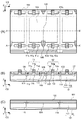
添付の図面を参照しつつ本発明の実施形態について以下に説明する。様々な実施形態を通じて同様の要素には同一の参照符号を付して重複する説明を省略する。本発明は一般にMOSトランジスタと、素子間を分離する不純物拡散層とを有する半導体装置に対して適用可能であり、以下ではこのような半導体装置の一例としてCMOS型の固体撮像装置を扱う。図1は本発明の様々な実施形態に係る製造方法によって製造される固体撮像装置100の構成の一例を説明するレイアウト図である。図1(a)は固体撮像装置100の平面図を示し、図1(b)および図1(c)はそれぞれ図1(a)のA−A’線およびB−B’線における断面図を示す。図2から図8においても同様に(a)が平面図を示し、(b)および(c)がそれぞれ各平面図におけるA−A’線およびB−B’線における断面図を示す。
Embodiments of the present invention will be described below with reference to the accompanying drawings. Throughout various embodiments, the same elements are denoted by the same reference numerals, and redundant description is omitted. The present invention is generally applicable to a semiconductor device having a MOS transistor and an impurity diffusion layer that separates elements, and hereinafter, a CMOS type solid-state imaging device is treated as an example of such a semiconductor device. FIG. 1 is a layout diagram illustrating an example of the configuration of a solid-
固体撮像装置100は、複数の画素が二次元状(アレイ状)に配置された画素アレイ、該画素アレイにおける行を選択する行選択回路、該画素アレイにおける列を選択する列選択回路、列信号線を介して該画素アレイから信号を読み出す読み出し回路を含みうる。画素アレイ、行選択回路、列選択回路および読み出し回路は、半導体基板101に形成される。典型的には、読み出し回路は、該画素アレイにおける該行選択回路によって選択された行の画素の信号を読み出し、該列選択回路は、該読み出し回路によって読み出された1行分の画素の信号の中から外部に出力すべき信号を選択する。
The solid-
固体撮像装置100の各画素は同様の構成を有しうるので、図1では1つの画素PXLとその周辺の画素の一部分とを示し、画素PXLについて説明する。図1では説明のために画素の境界を点線で示す。場合によっては、この点線が直線でない場合も有り得る。半導体基板101は、例えば半導体領域102とその上に配置されたウェル領域103(不純物半導体領域ともいう)とを含みうる。半導体領域102は、第1導電型のシリコン基板でありうる。ウェル領域103は、第1導電型でありうる。ウェル領域103の中には、第1導電型の蓄積領域104が形成されうる。半導体基板101の表面(ウェル領域103の表面)には酸化膜等の絶縁膜107が形成され、該絶縁膜107の上には転送ゲート106が形成されている。ここで、第1導電型がN型であり第2導電型がP型である場合は蓄積領域104には電子が蓄積され、第1導電型がP型であり第2導電型がN型である場合は蓄積領域104には正孔が蓄積される。以下では説明のために第1導電型がN型であり、第2導電型がP型である場合を扱うが、その逆でも本発明は成り立つ。
Since each pixel of the solid-
画素PXLは蓄積領域104、電荷電圧変換部105(フローティングディフュージョン)および転送ゲート106を有する。光電変換素子は少なくとも蓄積領域104とウェル領域103とによって形成され、固体撮像装置100への入射光によって光電変換素子で発生した電荷は、当該光電変換素子の蓄積領域104に蓄積される。転送ゲート106は、MOSトランジスタのゲートとして機能する。行選択回路から転送ゲート106にアクティブレベルの電圧が供給されることによって転送ゲート106の下にMOSトランジスタのチャネルが形成され、蓄積領域104に蓄積された電荷がこのチャネルを通して電荷電圧変換部105に転送される。このチャネルが出来る領域を含み、ゲートの下にあり、ソースとドレインとの間にある領域をチャネル領域と称する。
The pixel PXL includes a
画素PXLは電荷電圧変換部105の電圧をリセットするリセットスイッチや、電荷電圧変換部105の電圧に応じた信号を列信号線に出力する増幅部や、画素を選択するための選択スイッチ等として機能する1つ以上のMOSトランジスタを含みうる。その他のMOSトランジスタとして、光電変換素子の電荷と隣接する光電変換素子の電荷とを加算するためのスイッチ等も挙げられる。これらのMOSトランジスタのうちの1つをMOSトランジスタT1(第1MOSトランジスタ)とよび、別のものをMOSトランジスタT2(第2MOSトランジスタ)とよぶ。MOSトランジスタT1、T2は何れの機能を有するトランジスタであってもよい。本実施形態では、MOSトランジスタT1、T2のいずれもN型である場合を扱うが、少なくとも一方がP型であってもよい。MOSトランジスタT1は、半導体基板101内のウェル領域103のアクティブ領域に形成されたソースT1s、ドレインT1dと、ソースT1sおよびドレインT1dの間のチャネル領域に形成されたイオン導入層(注入層)T1iとを有しうる。MOSトランジスタT1はさらにチャネル領域を覆うように半導体基板101の絶縁膜107の上に形成されたゲートT1gを有しうる。MOSトランジスタT2もMOSトランジスタT1と同様に、ソースT2s、ドレインT2d、イオン導入層(注入層)T2iおよびゲートT2gを有しうる。固体撮像装置100はさらに、トランジスタT1、T2の下にP型の不純物拡散層112を有しうる。
The pixel PXL functions as a reset switch that resets the voltage of the charge-
固体撮像装置100では各画素が電荷電圧変換部105とMOSトランジスタT1、T2とを有しているが、複数の画素が電荷電圧変換部105とMOSトランジスタT1、T2とを共有してもよい。また、固体撮像装置100は電荷電圧変換部105やMOSトランジスタT1、T2に接続される配線層を有しうるが、配線層は周知の構成と同じであってもよいため、説明および図示を省略する。
In the solid-
固体撮像装置100はまた、半導体基板101の表面に形成された絶縁膜107と蓄積領域104との間に形成されたP型の拡散層108を有する。固体撮像装置100はさらに、MOSトランジスタT1、T2を他の素子から分離するための酸化膜等の絶縁膜109、および絶縁膜109の直下に配置されたチャネルストップとして機能するP型の半導体層111を有しうる。固体撮像装置100はさらに、隣接する画素の光電変換素子を分離するP型の不純物拡散層110を有しうる。不純物拡散層110は隣接する画素の光電変換素子の間に配置され、特にこれらの画素の蓄積領域104の間に配置されうる。
The solid-
説明のために、各図に示すような座標系CSを設定する。この座標系CSでは、XY平面が半導体基板101の表面に平行であり、Z軸が半導体基板101の表面の法線に平行である。本実施形態では、X方向に隣接した2つの画素の蓄積領域104の間に電荷電圧変換部105やMOSトランジスタT1、T2が形成され、Y方向に隣接した2つの画素の蓄積領域104の間には他の素子が形成されずに不純物拡散層110が形成される。以下の説明において、半導体領域の形成される範囲を図面に示しているが、あくまで模式的なものである。
For explanation, a coordinate system CS as shown in each figure is set. In this coordinate system CS, the XY plane is parallel to the surface of the
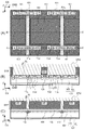
続いて、図2から図4を用いて図1に示した固体撮像装置100の製造方法の第1実施形態を説明する。まず、図2に示される半導体基板101を準備する。この半導体基板101には、ウェル領域103、電荷電圧変換部105、絶縁膜107、109、半導体層111、拡散層108、ソースT1s、T2s、ドレインT1d、T2dが形成されている。また、半導体基板101の上に転送ゲート106およびゲートT1g、T2gが形成されている。以下の各実施形態における製造方法では、説明を簡単にするため、転送ゲート106およびゲートT1g、T2gは不図示である。このような半導体基板101を形成する方法は周知の技術を用いればよいため、その説明を省略する。次に、半導体基板101の上にフォトリソグラフィー工程によってレジストパターンRPを形成する。レジストパターンRPは図2に示すような開口OPと遮蔽部SDとを有する。本実施形態では、レジストパターンRPは、Z軸方向から半導体基板101を見た場合に、遮蔽部SDによって蓄積領域104と電荷電圧変換部105とを覆う。また、レジストパターンRPは、Z軸方向から半導体基板101を見た場合に、MOSトランジスタT1、T2のチャネル領域(ソースとドレインとの間の領域)と、隣接する蓄積領域104の間の領域(以下、蓄積領域分離領域とよぶ)とを開口OPから露出する。
Next, a first embodiment of a method for manufacturing the solid-
続いて、図3に示すように、Z軸に平行な方向DR1(第1方向)、すなわち半導体基板101の表面に直交する方向DR1に沿ってイオンを照射(注入)する工程を行う。つまり、イオン照射方向(注入方向)が方向DR1である。ここで、方向DR1は半導体基板の表面の法線に対して0度である。本明細書において、方向は座標系CSにおける空間ベクトルによって規定される。レジストパターンRPは、方向DR1から半導体基板101を見た場合に、蓄積領域104および電荷電圧変換部105を遮蔽部SDによって遮り、蓄積領域分離領域およびMOSトランジスタT1、T2が形成される領域を開口OPから露出する。そのため、レジストパターンRPの開口OPを通過したイオンは、半導体基板101の表面のうち、図3(a)の斜線部301で示す部分に到達し、半導体基板101内に注入される。ここで注入されるイオンは例えばホウ素やインジウムなどのP型半導体領域を形成するためのイオンである。蓄積領域分離領域に注入されたイオンは半導体基板101内にP型の不純物拡散層110を形成する。また、MOSトランジスタT1、T2が形成される領域に注入されたイオンはこれらのトランジスタのソースT1s、T2sおよびドレインT1d、T2dの下にP型の不純物拡散層112を形成する。
Subsequently, as shown in FIG. 3, a step of irradiating (implanting) ions along a direction DR1 (first direction) parallel to the Z-axis, that is, a direction DR1 orthogonal to the surface of the
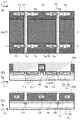
続いて、図4に示すように、YZ平面に平行で、Z軸から傾いた方向DR2(第2方向)に沿ってイオンを照射(注入)する工程を行う。つまり、イオン照射方向(注入方向)が方向DR2である。ここで、方向DR2は半導体基板の表面の法線NLに対して角度θを有する。これにより、レジストパターンRPの開口OPを通過したイオンが、半導体基板101の表面のうち、図4(a)の斜線部401で示す部分に到達し、半導体基板101内に注入される。MOSトランジスタT1、T2の閾値電圧を上昇したい場合にはボロンなどのドナーイオンを注入し、この閾値電圧を低下したい場合には砒素や燐などのアクセプタイオンを注入する。レジストパターンRPは、方向DR2から半導体基板101を見た場合に、蓄積領域104、電荷電圧変換部105および蓄積領域分離領域を遮蔽部SDによって遮り、MOSトランジスタT1、T2が形成される領域を開口OPから露出する。そのため、MOSトランジスタT1、T2が形成される領域に注入されたイオンはこれらのトランジスタのチャネル領域にイオン導入層T1i、T2iを形成する。一方で、蓄積領域分離領域へ向けて照射されたイオンはレジストパターンRPの遮蔽部SDに遮蔽されて、半導体基板101に到達しない。レジストパターンRPは半導体基板に垂直な側面を有しているので、この遮蔽される領域の一辺をDSDとすると、レジストパターンRPの厚さDRPとイオン注入方向の角度θから、DSD=tanθ×DRPの関係がある。ここで、所望のDSDを有するために、レジストパターンの厚さDRPやイオン注入方向の角度θを設定できる。
Subsequently, as shown in FIG. 4, a step of irradiating (implanting) ions along a direction DR2 (second direction) parallel to the YZ plane and inclined from the Z axis is performed. That is, the ion irradiation direction (implantation direction) is the direction DR2. Here, the direction DR2 has an angle θ with respect to the normal NL of the surface of the semiconductor substrate. Thereby, ions that have passed through the opening OP of the resist pattern RP reach the portion indicated by the hatched
このように、方向DR2から半導体基板101を見た場合に、隣接する蓄積領域104を分離する領域はレジストパターンRPの遮蔽部SDの陰になるため、この領域にはMOSトランジスタT1、T2の閾値電圧を調整するためのイオンが導入されない。そのため、このイオンによる蓄積領域104を分離する不純物拡散層110の分離特性がこのイオンにより低下すること、または蓄積領域104の特性がこのイオンにより低下することを防止できる。また、MOSトランジスタT1、T2の下には不純物拡散層112が形成されるが、不純物拡散層112はイオン導入層T1i、T2iよりも深くに位置し、ウェル領域103よりも高濃度である。この不純物拡散層112は、N型のウェル領域103に配置されるN型のMOSトランジスタT1、T2を動作させるためのポテンシャルバリアとして機能可能である。なお、転送ゲート106は、これらイオン注入工程(照射工程)が終了した後に形成することも可能である。以上の工程を経て、図1の固体撮像装置100が製造される。
As described above, when the
本実施形態のCMOS型の固体撮像装置においては、増幅部のMOSトランジスタの閾値は信号のダイナミックレンジやノイズに大きな影響を与えるため、増幅部のMOSトランジスタにイオン導入層を形成することが好ましい。本実施形態では、MOSトランジスタT1を増幅部のMOSトランジスタとし、N型の半導体領域を形成するためのイオンを注入してN型のイオン導入層T1iを形成する。増幅部のMOSトランジスタT1をノイズが低減可能な埋め込みチャネル型のMOSトランジスタとして形成するためである。また、MOSトランジスタT2をリセットスイッチとし、N型の半導体領域を形成するためのイオンをN型のイオン導入層T2iを形成する。ここでは、リセットスイッチの閾値の設定に合わせて、N型あるいはP型のイオン導入層T2iを形成できる。 In the CMOS type solid-state imaging device of the present embodiment, since the threshold value of the MOS transistor in the amplifying unit greatly affects the signal dynamic range and noise, it is preferable to form an iontophoretic layer in the MOS transistor in the amplifying unit. In the present embodiment, the MOS transistor T1 is used as an amplifying portion MOS transistor, and ions for forming an N-type semiconductor region are implanted to form an N-type ion introduction layer T1i. This is because the MOS transistor T1 in the amplifying part is formed as a buried channel type MOS transistor capable of reducing noise. Further, the MOS transistor T2 is used as a reset switch, and ions for forming an N-type semiconductor region are formed in an N-type ion introduction layer T2i. Here, the N-type or P-type ion introduction layer T2i can be formed in accordance with the threshold setting of the reset switch.
上記の実施形態では、2つのイオン注入工程で共通のレジストパターンRPを使用することにより、レジストパターンの形成工程および剥離工程を低減でき、固体撮像装置100を安価かつ短時間で製造できる。上記の例では方向DR2が方向DR1よりも半導体基板101の表面の法線に対する角度が大きい場合を扱った。しかし、イオンを照射する方向を調整することによって、これらの角度を等しくしてもよいし、大小関係を逆にしてもよい。例えば、図3で説明した不純物拡散層110を形成するためのイオンを、XZ平面に平行で、Z軸から傾いた方向に沿って注入してもよい。この方向から半導体基板101を見た場合に、レジストパターンRPは、蓄積領域104、電荷電圧変換部105およびMOSトランジスタT1、T2が形成される領域を遮蔽部SDによって遮る。また、この方向から半導体基板101を見た場合に、レジストパターンRPは、蓄積領域分離領域を開口OPから露出する。そのため、不純物拡散層110は形成されるが、MOSトランジスタT1、T2の下にある不純物拡散層112は形成されない。
In the above embodiment, by using the common resist pattern RP in the two ion implantation steps, the resist pattern forming step and the peeling step can be reduced, and the solid-
続いて、図5を用いて図1に示した固体撮像装置100の製造方法の第2実施形態を説明する。第2実施形態では、図4を用いて説明したイオン注入工程までは第1実施形態と同様であり、その後にYZ平面に平行で、Z軸から傾いた方向DR3(第3方向)からイオンを注入する工程をさらに行う。方向DR2と方向DR3とは互いに異なる。本実施例では、半導体基板101の表面の法線と方向DR3との成す角は、半導体基板101の表面の法線と方向DR2との成す角よりも大きい。ここで表面の法線と方向が成す角とは、当該法線と、方向に沿った直線とがなす角度(90度以下)をいう。第1実施形態におけるイオン注入方向の角度θを用いると、第3方向の角度θ3は第2方向の角度θと、θ<θ3となる。そのため、レジストパターンRPは、方向DR3から半導体基板101を見た場合に、蓄積領域104、電荷電圧変換部105、蓄積領域分離領域およびMOSトランジスタT1が形成される領域を遮蔽部SDによって遮る。また、レジストパターンRPは、方向DR3から半導体基板101を見た場合に、MOSトランジスタT2が形成される領域を開口OPから露出する。これにより、レジストパターンRPの開口OPを通過したイオンが、半導体基板101の表面のうち、図5(a)の斜線部501で示す部分に到達し、半導体基板101内に導入される。このイオンにより、MOSトランジスタT1のイオン導入層T1iの濃度は更に高くなる。しかし、MOSトランジスタT2のイオン導入層T2iには方向DR3から注入されたイオンは到達しないので、イオン導入層T2iの濃度は変わらない。また、蓄積領域分離領域に向けて照射されたイオンはレジストパターンRPの遮蔽部SDに遮蔽されて、半導体基板101に到達しない。
Next, a second embodiment of the method for manufacturing the solid-
MOSトランジスタT1にはイオン導入層T1iを形成する必要があるが、MOSトランジスタT2にはイオン導入層T2iを形成する必要がない場合には、図5に示すイオン注入工程を行い、図4に示すイオン注入工程を省略すればよい。 If it is necessary to form the ion introduction layer T1i in the MOS transistor T1, but it is not necessary to form the ion introduction layer T2i in the MOS transistor T2, the ion implantation step shown in FIG. What is necessary is just to omit an ion implantation process.
第2実施形態では、複数のMOSトランジスタの閾値電圧が異なるようにできるため、第1実施形態の利点に加えて、固体撮像装置100の性能を向上できる。
In the second embodiment, the threshold voltages of the plurality of MOS transistors can be made different. Therefore, in addition to the advantages of the first embodiment, the performance of the solid-
続いて、図6および図7を用いて図1に示した固体撮像装置100の製造方法の第3実施形態を説明する。第3実施形態では、図3を用いて説明したイオン注入工程までは第1実施形態と同様である。その後に図6に示されるようなYZ平面に平行で、Z軸から傾いた方向DR4に沿ってイオンを注入する工程と、図7に示されるようなZ軸から傾いた方向DR5に沿ってイオンを注入する工程とをさらに行う。本実施例では、方向DR4(第2方向)と方向DR5(第3方向)とは半導体基板101との成す角が同じであり、XZ平面に関して面対称である。
Next, a third embodiment of the method for manufacturing the solid-
図6に示すように、レジストパターンRPは、方向DR4から半導体基板101を見た場合に、蓄積領域104、電荷電圧変換部105、蓄積領域分離領域およびMOSトランジスタT1が形成される領域を遮蔽部SDによって遮る。また、レジストパターンRPは、方向DR4から半導体基板101を見た場合に、MOSトランジスタT2が形成される領域を開口OPから露出する。そのため、方向DR4から照射され、レジストパターンRPの開口OPを通過したイオンは、半導体基板101の表面のうち、図6(a)の斜線部601で示す部分に到達し、半導体基板101内に注入される。このイオンにより、MOSトランジスタT1のチャネル領域にイオン導入層T1iが形成される。しかし、MOSトランジスタT2のチャネル領域には方向DR4から注入されたイオンは到達しないので、この工程ではイオン導入層T2iは形成されない。
As shown in FIG. 6, when the
図7に示すように、レジストパターンRPは、方向DR4から半導体基板101を見た場合に、蓄積領域104、電荷電圧変換部105、蓄積領域分離領域およびMOSトランジスタT2が形成される領域を遮蔽部SDによって遮る。また、レジストパターンRPは、方向DR4から半導体基板101を見た場合に、MOSトランジスタT1が形成される領域を開口OPから露出する。そのため、方向DR5から照射され、レジストパターンRPの開口OPを通過したイオンは、半導体基板101の表面のうち、図7(a)の斜線部701で示す部分に到達し、半導体基板101内に注入される。このイオンにより、MOSトランジスタT2のチャネル領域にイオン導入層T2iが形成される。しかし、MOSトランジスタT1のチャネル領域には方向DR4から注入されたイオンは到達しないので、この工程ではイオン導入層T1iの濃度は変わらない。
As shown in FIG. 7, when the
また、図6および図7のイオン注入工程の両方において、隣接する画素の蓄積領域104の間を露出する開口OPから注入されたイオンはレジストパターンRPの遮蔽部SDに遮蔽されて、半導体基板101に到達しない。
6 and 7, ions implanted from the opening OP that exposes between the
また、MOSトランジスタT1、T2のうちの一方のみにイオン導入層を形成する場合には、図6のイオン注入工程と図7のイオン注入工程のどちらか一方を実施すればよい。 Further, in the case where the ion introduction layer is formed only in one of the MOS transistors T1 and T2, one of the ion implantation process of FIG. 6 and the ion implantation process of FIG.
第3実施形態では、複数のMOSトランジスタの閾値電圧を独立して制御できるため、第1実施形態および第2実施形態の利点に加えて、MOSトランジスタの閾値電圧の調整の自由度が高まる。例えば、それぞれのMOSトランジスタの閾値電圧を調整するために異なるイオン種を用いることもできる。 In the third embodiment, since the threshold voltages of a plurality of MOS transistors can be controlled independently, the degree of freedom in adjusting the threshold voltages of the MOS transistors is increased in addition to the advantages of the first and second embodiments. For example, different ion species can be used to adjust the threshold voltage of each MOS transistor.
続いて、図8を参照して上述の実施形態の変形例を説明する。第1実施形態に対して変形例を適用した場合を説明するが、第2実施形態や第3実施形態にも適用できる。この変形例では、レジストパターンRPの開口OPは蓄積領域104の中央部分をさらに露出する。これにより、図3のイオン注入工程において、蓄積領域104の中央部分にもP型の不純物拡散層110が形成される。これにより、N型の蓄積領域104に蓄積された電荷を電荷電圧変換部105に転送する転送効率が向上しうる。この内側の領域を開口する部分の開口OPの大きさは、図4のイオン注入工程においてイオンが到達しない程度に形成しうる。このため、蓄積領域104の内側に形成された不純物拡散層110はMOSトランジスタの閾値電圧を調整するためのイオンの影響を受けない。
Subsequently, a modification of the above-described embodiment will be described with reference to FIG. Although the case where a modification is applied with respect to 1st Embodiment is demonstrated, it is applicable also to 2nd Embodiment and 3rd Embodiment. In this modification, the opening OP of the resist pattern RP further exposes the central portion of the
上述の実施形態では、画素の構成に限って説明してきたが、読み出し回路等の回路のトランジスタにも適用可能である。また、上述の実施形態では2つのMOSトランジスタの閾値電圧を調整する方法を説明してきたが、レジストパターンの厚さや開口の位置・大きさ、イオンを導入する方向を調整することによって、3つ以上のMOSトランジスタの閾値電圧を調整することもできる。各実施形態は組み合わせ可能である。また、上記ではCOMS型固体撮像装置を例として説明したが、他の形態の固体撮像装置に適用可能である。また、例えばMOSトランジスタを有するメモリセルの信号保持部を分離する不純物拡散層と、該MOSトランジスタの閾値電圧を調整するイオン導入層とを有する記憶装置などの半導体装置にも適用可能である。また、各実施形態における複数のイオン注入工程は上述した順番後は異なる順番で実施されてもよいし、同時に実施されてもよい。同時に実施するためには、例えば、イオンを発生するイオン源、イオンを輸送するビームライン、イオンを加速する加速管を含むイオン注入機構を2系統有するイオン注入装置を準備すればよい。イオン注入工程は、熱処理工程を伴っていてもよい。
本発明の半導体装置の製造方法によれば、少なくとも2つの領域を露出させる開口を有するレジストパターンを用い、異なる方向に沿って少なくとも2回のイオンを注入する工程を実施することで、2つの領域の半導体領域を作り分けることができる。
In the above-described embodiment, the description is limited to the pixel configuration, but the present invention can also be applied to a transistor of a circuit such as a readout circuit. In the above-described embodiment, the method for adjusting the threshold voltage of the two MOS transistors has been described. However, by adjusting the thickness of the resist pattern, the position / size of the opening, and the direction in which ions are introduced, three or more are adjusted. The threshold voltage of the MOS transistor can be adjusted. Each embodiment can be combined. In the above description, the COMS solid-state imaging device has been described as an example. However, the present invention is applicable to other forms of solid-state imaging devices. Further, the present invention can also be applied to a semiconductor device such as a memory device having an impurity diffusion layer for separating a signal holding portion of a memory cell having a MOS transistor and an iontophoretic layer for adjusting a threshold voltage of the MOS transistor. In addition, the plurality of ion implantation steps in each embodiment may be performed in a different order after the order described above, or may be performed simultaneously. In order to carry out simultaneously, for example, an ion implantation apparatus having two systems of ion implantation mechanisms including an ion source for generating ions, a beam line for transporting ions, and an acceleration tube for accelerating ions may be prepared. The ion implantation process may be accompanied by a heat treatment process.
According to the method of manufacturing a semiconductor device of the present invention, two regions are formed by performing a step of implanting ions at least twice along different directions using a resist pattern having an opening exposing at least two regions. It is possible to make different semiconductor regions.
Claims (9)
開口と遮蔽部とを有するレジストパターンを前記半導体基板の上に形成する形成工程と、
前記レジストパターンの前記開口を通じて前記半導体基板にイオンを注入する注入工程と
を有し、
前記形成工程で形成される前記レジストパターンは、
前記半導体基板を第1方向から見た場合に、前記分離領域を前記開口から露出し、
前記半導体基板を前記第1方向とは異なる方向から見た場合に、前記1つ以上のMOSトランジスタが形成される領域を前記開口から露出するとともに、前記分離領域を前記遮蔽部により遮り、
前記注入工程では、
前記第1方向に沿って照射されたイオンが前記分離領域に注入され、
前記異なる方向に沿って照射されたイオンが前記1つ以上のMOSトランジスタが形成される領域に注入され、
前記分離領域に注入されたイオンが、前記1つ以上のMOSトランジスタが形成される領域に注入されたイオンよりも、前記半導体基板の表面からの位置が深くなるようにイオンを照射する
ことを特徴とする固体撮像装置の製造方法。 A solid state in which a plurality of photoelectric conversion elements each including an accumulation region for accumulating charges and one or more MOS transistors are formed on a semiconductor substrate, and a separation region is provided between the adjacent accumulation regions of the semiconductor substrate. A method for manufacturing an imaging device, comprising:
Forming a resist pattern having an opening and a shielding portion on the semiconductor substrate;
And implanting ions into the semiconductor substrate through the openings of the resist pattern,
The resist pattern formed in the forming step is
When the semiconductor substrate is viewed from the first direction, the isolation region is exposed from the opening;
When the semiconductor substrate is viewed from a direction different from the first direction, a region where the one or more MOS transistors are formed is exposed from the opening, and the isolation region is shielded by the shielding part,
In the injection step,
Ions irradiated along the first direction are implanted into the separation region,
Ions irradiated along the different directions are implanted into regions where the one or more MOS transistors are formed ,
Ions are irradiated so that ions implanted in the isolation region are deeper from the surface of the semiconductor substrate than ions implanted in the region where the one or more MOS transistors are formed. > A method for manufacturing a solid-state imaging device.
前記異なる方向は互いに異なる第2方向及び第3方向を含み、
前記形成工程で形成される前記レジストパターンは、
前記半導体基板を前記第2方向から見た場合に、前記第1MOSトランジスタが形成される領域を前記開口から露出し、
前記半導体基板を前記第3方向から見た場合に、前記第2MOSトランジスタが形成される領域を前記開口から露出するとともに、前記第1MOSトランジスタが形成される領域を前記遮蔽部により遮り、
前記注入工程では、
前記第2方向に沿って照射されたイオンが前記第1MOSトランジスタが形成される領域に注入され
前記第3方向に沿って照射されたイオンが前記第2MOSトランジスタが形成される領域に注入される
ことを特徴とする請求項1乃至5の何れか1項に記載の固体撮像装置の製造方法。 The one or more MOS transistors include a first MOS transistor and a second MOS transistor;
The different directions include different second and third directions;
The resist pattern formed in the forming step is
When the semiconductor substrate is viewed from the second direction, a region where the first MOS transistor is formed is exposed from the opening,
When the semiconductor substrate is viewed from the third direction, a region where the second MOS transistor is formed is exposed from the opening, and a region where the first MOS transistor is formed is shielded by the shielding part,
In the injection step,
Ions irradiated along the second direction are implanted into a region where the first MOS transistor is formed, and ions irradiated along the third direction are implanted into a region where the second MOS transistor is formed. The method for manufacturing a solid-state imaging device according to claim 1, wherein:
前記半導体基板を前記第1方向から見た場合に、前記蓄積領域が形成される領域の中央部分を前記開口から露出し、
前記半導体基板を前記異なる方向から見た場合に、前記中央部分を前記遮蔽部により遮り、
前記注入工程では、
前記第1方向に沿って照射されたイオンが前記中央部分に注入される
ことを特徴とする請求項1乃至7の何れか1項に記載の固体撮像装置の製造方法。 The resist pattern formed in the forming step is
When the semiconductor substrate is viewed from the first direction, a central portion of a region where the accumulation region is formed is exposed from the opening,
When the semiconductor substrate is viewed from the different direction, the central portion is blocked by the shielding portion,
In the injection step,
The method for manufacturing a solid-state imaging device according to claim 1, wherein ions irradiated along the first direction are implanted into the central portion.
前記MOSトランジスタが形成される領域を含む第1領域と、前記第1領域と異なる領域で、隣接する前記蓄積領域の間に位置する分離領域を含む第2領域と、を露出させる開口を有するレジストパターンを前記半導体基板の上に形成する形成工程と、
前記レジストパターンの前記開口を通じて前記半導体基板にイオンを注入する注入工程と、を有し、
前記注入工程は、
第1の角度で、少なくとも前記第2領域にイオンを注入する工程と、
前記第1の角度とは異なる第2の角度で、前記第1領域のみにイオンを注入する工程と、
を有し、
前記第1の角度で前記第2領域に注入されたイオンが、前記第2の角度で前記第1領域に注入されたイオンよりも、前記半導体基板の表面からの位置が深くなるようにイオンを照射する
ことを特徴とする固体撮像装置の製造方法。 A method of manufacturing a solid-state imaging device in which a plurality of photoelectric conversion elements each including an accumulation region for accumulating charges and a MOS transistor are formed on a semiconductor substrate,
A resist having an opening exposing a first region including a region where the MOS transistor is formed and a second region including a separation region located between the adjacent storage regions in a region different from the first region. Forming a pattern on the semiconductor substrate;
And implanting ions into the semiconductor substrate through the openings of the resist pattern,
The injection step includes
Implanting ions at least in the second region at a first angle;
Implanting ions only in the first region at a second angle different from the first angle;
I have a,
The ions implanted in the second region at the first angle are deeper than the ions implanted in the first region at the second angle so that the position from the surface of the semiconductor substrate is deeper. Irradiating a method for manufacturing a solid-state imaging device.
Priority Applications (2)
| Application Number | Priority Date | Filing Date | Title |
|---|---|---|---|
| JP2011223457A JP5922905B2 (en) | 2011-10-07 | 2011-10-07 | Method for manufacturing solid-state imaging device |
| US13/607,107 US8835269B2 (en) | 2011-10-07 | 2012-09-07 | Method of manufacturing solid-state image sensor |
Applications Claiming Priority (1)
| Application Number | Priority Date | Filing Date | Title |
|---|---|---|---|
| JP2011223457A JP5922905B2 (en) | 2011-10-07 | 2011-10-07 | Method for manufacturing solid-state imaging device |
Publications (3)
| Publication Number | Publication Date |
|---|---|
| JP2013084754A JP2013084754A (en) | 2013-05-09 |
| JP2013084754A5 JP2013084754A5 (en) | 2014-11-20 |
| JP5922905B2 true JP5922905B2 (en) | 2016-05-24 |
Family
ID=48042336
Family Applications (1)
| Application Number | Title | Priority Date | Filing Date |
|---|---|---|---|
| JP2011223457A Active JP5922905B2 (en) | 2011-10-07 | 2011-10-07 | Method for manufacturing solid-state imaging device |
Country Status (2)
| Country | Link |
|---|---|
| US (1) | US8835269B2 (en) |
| JP (1) | JP5922905B2 (en) |
Families Citing this family (2)
| Publication number | Priority date | Publication date | Assignee | Title |
|---|---|---|---|---|
| US9000500B2 (en) * | 2009-12-30 | 2015-04-07 | Omnivision Technologies, Inc. | Image sensor with doped transfer gate |
| JP2016058635A (en) * | 2014-09-11 | 2016-04-21 | ルネサスエレクトロニクス株式会社 | Semiconductor device manufacturing method |
Family Cites Families (8)
| Publication number | Priority date | Publication date | Assignee | Title |
|---|---|---|---|---|
| TW421962B (en) | 1997-09-29 | 2001-02-11 | Canon Kk | Image sensing device using mos type image sensing elements |
| JP3487575B2 (en) | 1997-12-26 | 2004-01-19 | キヤノン株式会社 | Photoelectric conversion device |
| JP2000021995A (en) * | 1998-06-26 | 2000-01-21 | Hitachi Ltd | Manufacture of semiconductor integrated circuit device |
| US6743652B2 (en) * | 2002-02-01 | 2004-06-01 | Stmicroelectronics, Inc. | Method for making an integrated circuit device including photodiodes |
| JP2004079813A (en) * | 2002-08-19 | 2004-03-11 | Matsushita Electric Ind Co Ltd | Semiconductor device fabricating process |
| JP2005093866A (en) * | 2003-09-19 | 2005-04-07 | Fuji Film Microdevices Co Ltd | Manufacturing method of solid-state imaging device |
| JP2007299938A (en) | 2006-04-28 | 2007-11-15 | Sharp Corp | Solid state imaging apparatus, its manufacturing method, and electronic information instrument |
| JP2008060380A (en) | 2006-08-31 | 2008-03-13 | Matsushita Electric Ind Co Ltd | Solid-state imaging device and its manufacturing method |
-
2011
- 2011-10-07 JP JP2011223457A patent/JP5922905B2/en active Active
-
2012
- 2012-09-07 US US13/607,107 patent/US8835269B2/en active Active
Also Published As
| Publication number | Publication date |
|---|---|
| US8835269B2 (en) | 2014-09-16 |
| JP2013084754A (en) | 2013-05-09 |
| US20130089945A1 (en) | 2013-04-11 |
Similar Documents
| Publication | Publication Date | Title |
|---|---|---|
| JP5539104B2 (en) | Photoelectric conversion device and imaging system using the same | |
| US7592579B2 (en) | Photoelectric conversion device manufacturing method, semiconductor device manufacturing method, photoelectric conversion device, and image sensing system | |
| US9768213B2 (en) | Solid-state image sensor and camera | |
| JP5539029B2 (en) | Method for manufacturing solid-state imaging device | |
| US9711558B2 (en) | Imaging device with photoelectric converter | |
| US10121816B2 (en) | Imaging device and method of manufacturing imaging device | |
| KR101390518B1 (en) | Solid-state image pickup device | |
| JP2009158932A (en) | Image sensor, and manufacturing method therefor | |
| JP6246076B2 (en) | Semiconductor device manufacturing method and semiconductor device | |
| JP5539373B2 (en) | Solid-state imaging device and manufacturing method thereof | |
| US7755150B2 (en) | MOS solid-state image pickup device and manufacturing method thereof | |
| US8383497B2 (en) | Method for manufacturing solid-state image sensor | |
| WO2006130545A2 (en) | Cmos active pixel sensor shared amplifier pixel | |
| JP5922905B2 (en) | Method for manufacturing solid-state imaging device | |
| KR101442358B1 (en) | Solid-state image pickup device and method for manufacturing the same | |
| JP2017054966A (en) | Method of manufacturing semiconductor device and semiconductor device | |
| US10483302B2 (en) | Solid-state imaging device | |
| US9231021B2 (en) | Image pickup apparatus, image pickup system, and image pickup apparatus manufacturing method | |
| JP2016058635A (en) | Semiconductor device manufacturing method | |
| JP2016225597A (en) | Solid-state image sensor and camera | |
| JP2020057689A (en) | Solid-state imaging device and manufacturing method thereof | |
| JP2005109439A (en) | Solid-state image pickup device and manufacturing method of the same | |
| JP2021190614A (en) | Photoelectric conversion device and manufacturing method for the same | |
| JP2014146804A (en) | Photoelectric conversion device and image pickup system |
Legal Events
| Date | Code | Title | Description |
|---|---|---|---|
| A521 | Written amendment |
Free format text: JAPANESE INTERMEDIATE CODE: A523 Effective date: 20141007 |
|
| A621 | Written request for application examination |
Free format text: JAPANESE INTERMEDIATE CODE: A621 Effective date: 20141007 |
|
| A977 | Report on retrieval |
Free format text: JAPANESE INTERMEDIATE CODE: A971007 Effective date: 20150618 |
|
| A131 | Notification of reasons for refusal |
Free format text: JAPANESE INTERMEDIATE CODE: A131 Effective date: 20150703 |
|
| A521 | Written amendment |
Free format text: JAPANESE INTERMEDIATE CODE: A523 Effective date: 20150806 |
|
| TRDD | Decision of grant or rejection written | ||
| A01 | Written decision to grant a patent or to grant a registration (utility model) |
Free format text: JAPANESE INTERMEDIATE CODE: A01 Effective date: 20160318 |
|
| A61 | First payment of annual fees (during grant procedure) |
Free format text: JAPANESE INTERMEDIATE CODE: A61 Effective date: 20160415 |
|
| R151 | Written notification of patent or utility model registration |
Ref document number: 5922905 Country of ref document: JP Free format text: JAPANESE INTERMEDIATE CODE: R151 |