JP5539104B2 - 光電変換装置およびそれを用いた撮像システム - Google Patents
光電変換装置およびそれを用いた撮像システム Download PDFInfo
- Publication number
- JP5539104B2 JP5539104B2 JP2010185289A JP2010185289A JP5539104B2 JP 5539104 B2 JP5539104 B2 JP 5539104B2 JP 2010185289 A JP2010185289 A JP 2010185289A JP 2010185289 A JP2010185289 A JP 2010185289A JP 5539104 B2 JP5539104 B2 JP 5539104B2
- Authority
- JP
- Japan
- Prior art keywords
- photoelectric conversion
- semiconductor region
- region
- transistor
- conversion element
- Prior art date
- Legal status (The legal status is an assumption and is not a legal conclusion. Google has not performed a legal analysis and makes no representation as to the accuracy of the status listed.)
- Active
Links
- 238000006243 chemical reaction Methods 0.000 title claims description 124
- 238000003384 imaging method Methods 0.000 title description 21
- 239000004065 semiconductor Substances 0.000 claims description 153
- 239000000758 substrate Substances 0.000 claims description 28
- 238000009825 accumulation Methods 0.000 claims description 13
- 230000003321 amplification Effects 0.000 claims description 13
- 238000003199 nucleic acid amplification method Methods 0.000 claims description 13
- 238000005468 ion implantation Methods 0.000 claims description 8
- 238000003860 storage Methods 0.000 claims description 8
- 238000000034 method Methods 0.000 claims description 3
- 238000002955 isolation Methods 0.000 description 11
- 238000009792 diffusion process Methods 0.000 description 10
- 230000004888 barrier function Effects 0.000 description 7
- 230000035945 sensitivity Effects 0.000 description 6
- 230000006866 deterioration Effects 0.000 description 5
- 238000000926 separation method Methods 0.000 description 5
- 238000010586 diagram Methods 0.000 description 4
- 230000006870 function Effects 0.000 description 4
- 150000002500 ions Chemical class 0.000 description 4
- 229920002120 photoresistant polymer Polymers 0.000 description 3
- 238000012937 correction Methods 0.000 description 2
- 238000002513 implantation Methods 0.000 description 2
- 239000012535 impurity Substances 0.000 description 1
- 238000010884 ion-beam technique Methods 0.000 description 1
- 238000004519 manufacturing process Methods 0.000 description 1
- 239000011159 matrix material Substances 0.000 description 1
- 230000003287 optical effect Effects 0.000 description 1
- 230000003647 oxidation Effects 0.000 description 1
- 238000007254 oxidation reaction Methods 0.000 description 1
- 230000003071 parasitic effect Effects 0.000 description 1
Images


Classifications
-
- H—ELECTRICITY
- H01—ELECTRIC ELEMENTS
- H01L—SEMICONDUCTOR DEVICES NOT COVERED BY CLASS H10
- H01L27/00—Devices consisting of a plurality of semiconductor or other solid-state components formed in or on a common substrate
- H01L27/14—Devices consisting of a plurality of semiconductor or other solid-state components formed in or on a common substrate including semiconductor components sensitive to infrared radiation, light, electromagnetic radiation of shorter wavelength or corpuscular radiation and specially adapted either for the conversion of the energy of such radiation into electrical energy or for the control of electrical energy by such radiation
- H01L27/144—Devices controlled by radiation
- H01L27/146—Imager structures
- H01L27/148—Charge coupled imagers
- H01L27/14831—Area CCD imagers
-
- H—ELECTRICITY
- H01—ELECTRIC ELEMENTS
- H01L—SEMICONDUCTOR DEVICES NOT COVERED BY CLASS H10
- H01L27/00—Devices consisting of a plurality of semiconductor or other solid-state components formed in or on a common substrate
- H01L27/14—Devices consisting of a plurality of semiconductor or other solid-state components formed in or on a common substrate including semiconductor components sensitive to infrared radiation, light, electromagnetic radiation of shorter wavelength or corpuscular radiation and specially adapted either for the conversion of the energy of such radiation into electrical energy or for the control of electrical energy by such radiation
- H01L27/144—Devices controlled by radiation
- H01L27/146—Imager structures
- H01L27/14601—Structural or functional details thereof
- H01L27/14603—Special geometry or disposition of pixel-elements, address-lines or gate-electrodes
Description
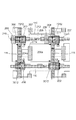
まず、本発明が適用されうる画素回路の一例について説明する。図2(A)は本発明が適用されうる画素回路の一例を示した回路図であり、図2(B)はその画素回路の1画素分の平面レイアウトを示す平面図である。以下、信号電荷が電子の場合を説明する。
本実施形態の光電変換装置について、図1及び図3を用いて説明する。まず、図1(A)は図2(B)の平面図に対応した平面図である。
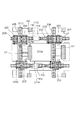
本実施形態の光電変換装置について図4を用いて説明する。図4は図3(B)に対応する断面模式図であり、図3(B)と同様の構成には、同一の符号を付し、説明を省略する。
本実施形態の光電変換装置について図5を用いて説明する。図5は図1に対応する断面模式図であり、図1と同様の構成には、同一の符号を付し、説明を省略する。
本実施形態の光電変換装置について図6を用いて説明する。図6において、図1と同一の構成には同一の符号を付し、説明を省略する。
本発明の光電変換装置を撮像装置として撮像システムに適用した場合の一実施例について詳述する。撮像システムとして、デジタルスチルカメラやデジタルカムコーダーや監視カメラなどがあげられる。図7に、撮像システムの例としてデジタルスチルカメラに光電変換装置を適用した場合のブロック図を示す。
201a 転送MOSトランジスタのゲート電極
204a 浮遊拡散部
110 第1導電型の第1の半導体領域
111 第1導電型の第3の半導体領域
1012 第1導電型の第2の半導体領域
Claims (9)
- 第1導電型の第1の電荷蓄積領域を含む第1の光電変換素子と、
前記第1の光電変換素子に対して第1方向に沿って配置され、前記第1導電型の第2の電荷蓄積領域を含む第2の光電変換素子と、
前記第1の光電変換素子に対して前記第1方向と交わる第2方向に沿って配置され、前記第1導電型の第3の電荷蓄積領域を含む第3の光電変換素子と、
前記第1の光電変換素子にて生じた信号電荷を読み出すためのトランジスタと、が配置された前記第1導電型と反対導電型の第2導電型の半導体領域を含む半導体基板を有する光電変換装置において、
前記第1の電荷蓄積領域と前記第2の電荷蓄積領域との間の前記第2導電型の半導体領域にイオン注入によって形成され、前記半導体基板の深さ方向において前記トランジスタのチャネル部となる部分よりも深くに位置し、前記第2の方向に沿って配され、第1の幅を有する前記第2導電型の第1の半導体領域と、
前記第1の電荷蓄積領域と前記第2の電荷蓄積領域との間の前記第2導電型の半導体領域にイオン注入によって形成され、前記半導体基板の表面へ投影した時に、前記第2導電型の半導体領域の前記トランジスタが配された領域に配置され、前記半導体領域基板の深さ方向において前記トランジスタのチャネル部となる部分の下部に位置し、前記第1の幅よりも広く、前記トランジスタのチャネル部となる部分の幅よりも広い第2の幅を有する前記第2導電型の第2の半導体領域と、
前記第1の電荷蓄積領域と前記第3の電荷蓄積領域との間の前記第2導電型の半導体領域にイオン注入によって形成され、前記半導体基板の深さ方向において前記トランジスタのチャネル部となる部分よりも深くに位置し、前記第1の方向に沿って配され、前記第2の幅よりも狭い第3の幅を有する前記第2導電型の第3の半導体領域と、を有し、
前記半導体基板の表面へ投影した時に、前記第1の半導体領域と前記第3の半導体領域は、格子状に配置し、
前記半導体基板の表面へ投影した時に、前記第2の半導体領域は、前記第1の半導体領域が構成する前記格子の辺の一部である光電変換装置。 - 前記第2の半導体領域は、前記トランジスタのチャネル部となる部分の長さよりも長い長さを有する請求項1に記載の光電変換装置。
- 前記第1の光電変換素子と、前記第2の光電変換素子は、前記トランジスタを共有化していることを特徴とする請求項1または2に記載の光電変換装置。
- 前記第1方向と前記第2方向は直交する請求項1乃至3のいずれか1項に記載の光電変換装置。
- 前記第2の半導体領域は、前記第1の半導体領域と接し、前記第3の半導体領域と接する請求項1乃至4のいずれか1項に記載の光電変換装置。
- 前記半導体基板の表面に投影した時に、
前記第1の半導体領域は、前記第2方向に長辺を有し、
前記第3の半導体領域は、前記第1方向に長辺を有し、
前記第2の半導体領域は、前記格子の交差部に設けられている請求項1乃至5のいずれか1項に記載の光電変換装置。 - 前記第1の電荷蓄積領域と前記第2の電荷蓄積領域との間において、前記第1の半導体領域が配されていない領域を有する請求項1乃至6のいずれか1項に記載の光電変換装置。
- 前記トランジスタは、リセットトランジスタおよび増幅トランジスタの少なくとも一方のトランジスタであって、
前記第2の半導体領域は、前記トランジスタのチャネル部となる部分の長さよりも長い長さを有する請求項1乃至7のいずれか1項に記載の光電変換装置。 - 請求項1乃至8のいずれか1項に記載の光電変換装置と、
前記光電変換装置から出力される信号を処理する信号処理回路と、を有する撮像システム。
Priority Applications (5)
| Application Number | Priority Date | Filing Date | Title |
|---|---|---|---|
| JP2010185289A JP5539104B2 (ja) | 2009-09-24 | 2010-08-20 | 光電変換装置およびそれを用いた撮像システム |
| US12/885,683 US8466401B2 (en) | 2009-09-24 | 2010-09-20 | Photoelectric conversion apparatus and imaging system using the photoelectric conversion apparatus |
| CN201310059322.9A CN103151363B (zh) | 2009-09-24 | 2010-09-21 | 光电转换装置和使用光电转换装置的成像系统 |
| CN2010102884333A CN102034838B (zh) | 2009-09-24 | 2010-09-21 | 光电转换装置和使用光电转换装置的成像系统 |
| US13/895,045 US8796609B2 (en) | 2009-09-24 | 2013-05-15 | Photoelectric conversion apparatus and imaging system using the photoelectric conversion apparatus |
Applications Claiming Priority (3)
| Application Number | Priority Date | Filing Date | Title |
|---|---|---|---|
| JP2009219218 | 2009-09-24 | ||
| JP2009219218 | 2009-09-24 | ||
| JP2010185289A JP5539104B2 (ja) | 2009-09-24 | 2010-08-20 | 光電変換装置およびそれを用いた撮像システム |
Publications (3)
| Publication Number | Publication Date |
|---|---|
| JP2011091367A JP2011091367A (ja) | 2011-05-06 |
| JP2011091367A5 JP2011091367A5 (ja) | 2014-01-16 |
| JP5539104B2 true JP5539104B2 (ja) | 2014-07-02 |
Family
ID=43755800
Family Applications (1)
| Application Number | Title | Priority Date | Filing Date |
|---|---|---|---|
| JP2010185289A Active JP5539104B2 (ja) | 2009-09-24 | 2010-08-20 | 光電変換装置およびそれを用いた撮像システム |
Country Status (3)
| Country | Link |
|---|---|
| US (2) | US8466401B2 (ja) |
| JP (1) | JP5539104B2 (ja) |
| CN (2) | CN103151363B (ja) |
Families Citing this family (18)
| Publication number | Priority date | Publication date | Assignee | Title |
|---|---|---|---|---|
| JP5558857B2 (ja) * | 2009-03-09 | 2014-07-23 | キヤノン株式会社 | 光電変換装置およびそれを用いた撮像システム |
| JP5539105B2 (ja) | 2009-09-24 | 2014-07-02 | キヤノン株式会社 | 光電変換装置およびそれを用いた撮像システム |
| JP5679653B2 (ja) | 2009-12-09 | 2015-03-04 | キヤノン株式会社 | 光電変換装置およびそれを用いた撮像システム |
| JP5656484B2 (ja) | 2010-07-07 | 2015-01-21 | キヤノン株式会社 | 固体撮像装置および撮像システム |
| JP5643555B2 (ja) | 2010-07-07 | 2014-12-17 | キヤノン株式会社 | 固体撮像装置及び撮像システム |
| JP5645513B2 (ja) | 2010-07-07 | 2014-12-24 | キヤノン株式会社 | 固体撮像装置及び撮像システム |
| JP5751766B2 (ja) | 2010-07-07 | 2015-07-22 | キヤノン株式会社 | 固体撮像装置および撮像システム |
| JP5885401B2 (ja) | 2010-07-07 | 2016-03-15 | キヤノン株式会社 | 固体撮像装置および撮像システム |
| JP5697371B2 (ja) | 2010-07-07 | 2015-04-08 | キヤノン株式会社 | 固体撮像装置および撮像システム |
| JP6274788B2 (ja) | 2013-08-28 | 2018-02-07 | キヤノン株式会社 | 撮像装置、撮像システム及び撮像装置の駆動方法 |
| JP2016058635A (ja) * | 2014-09-11 | 2016-04-21 | ルネサスエレクトロニクス株式会社 | 半導体装置の製造方法 |
| JP6562675B2 (ja) * | 2015-03-26 | 2019-08-21 | キヤノン株式会社 | 光電変換装置、撮像システム、光電変換装置の駆動方法 |
| JP6491519B2 (ja) * | 2015-04-02 | 2019-03-27 | キヤノン株式会社 | 撮像素子及び撮像装置 |
| JP6688165B2 (ja) | 2016-06-10 | 2020-04-28 | キヤノン株式会社 | 撮像装置及び撮像システム |
| JP7013119B2 (ja) | 2016-07-21 | 2022-01-31 | キヤノン株式会社 | 固体撮像素子、固体撮像素子の製造方法、及び撮像システム |
| CN108288439B (zh) * | 2017-01-10 | 2020-06-30 | 陈扬证 | 显示装置 |
| JP6904772B2 (ja) | 2017-04-26 | 2021-07-21 | キヤノン株式会社 | 固体撮像装置及びその駆動方法 |
| JP7245014B2 (ja) | 2018-09-10 | 2023-03-23 | キヤノン株式会社 | 固体撮像装置、撮像システム、および固体撮像装置の駆動方法 |
Family Cites Families (26)
| Publication number | Priority date | Publication date | Assignee | Title |
|---|---|---|---|---|
| JP3530159B2 (ja) | 2001-08-22 | 2004-05-24 | 松下電器産業株式会社 | 固体撮像装置およびその製造方法 |
| JP3702854B2 (ja) | 2002-03-06 | 2005-10-05 | ソニー株式会社 | 固体撮像素子 |
| JP2005268814A (ja) * | 2002-06-27 | 2005-09-29 | Canon Inc | 固体撮像装置及び固体撮像装置を用いたカメラシステム |
| JP4208559B2 (ja) | 2002-12-03 | 2009-01-14 | キヤノン株式会社 | 光電変換装置 |
| JP4514188B2 (ja) | 2003-11-10 | 2010-07-28 | キヤノン株式会社 | 光電変換装置及び撮像装置 |
| JP4508619B2 (ja) | 2003-12-03 | 2010-07-21 | キヤノン株式会社 | 固体撮像装置の製造方法 |
| JP3793202B2 (ja) | 2004-02-02 | 2006-07-05 | キヤノン株式会社 | 固体撮像装置 |
| JP3890333B2 (ja) | 2004-02-06 | 2007-03-07 | キヤノン株式会社 | 固体撮像装置 |
| JP4067054B2 (ja) | 2004-02-13 | 2008-03-26 | キヤノン株式会社 | 固体撮像装置および撮像システム |
| JP4230406B2 (ja) * | 2004-04-27 | 2009-02-25 | 富士通マイクロエレクトロニクス株式会社 | 固体撮像装置 |
| JP5230058B2 (ja) | 2004-06-07 | 2013-07-10 | キヤノン株式会社 | 固体撮像装置およびカメラ |
| US7605415B2 (en) | 2004-06-07 | 2009-10-20 | Canon Kabushiki Kaisha | Image pickup device comprising photoelectric conversation unit, floating diffusion region and guard ring |
| JP4459064B2 (ja) * | 2005-01-14 | 2010-04-28 | キヤノン株式会社 | 固体撮像装置、その制御方法及びカメラ |
| JP2006319003A (ja) * | 2005-05-10 | 2006-11-24 | Canon Inc | 撮像装置 |
| TWI310987B (en) * | 2005-07-09 | 2009-06-11 | Samsung Electronics Co Ltd | Image sensors including active pixel sensor arrays |
| US7423302B2 (en) | 2005-11-21 | 2008-09-09 | Digital Imaging Systems Gmbh | Pinned photodiode (PPD) pixel with high shutter rejection ratio for snapshot operating CMOS sensor |
| JP4275150B2 (ja) * | 2006-04-28 | 2009-06-10 | ヒロセ電機株式会社 | モジュラージャックを有する装置 |
| JP4928199B2 (ja) | 2006-09-07 | 2012-05-09 | キヤノン株式会社 | 信号検出装置、信号検出装置の信号読み出し方法及び信号検出装置を用いた撮像システム |
| JP2008078302A (ja) * | 2006-09-20 | 2008-04-03 | Canon Inc | 撮像装置および撮像システム |
| JP2008084962A (ja) | 2006-09-26 | 2008-04-10 | Toshiba Corp | 固体撮像装置及びその製造方法 |
| JP5142696B2 (ja) | 2007-12-20 | 2013-02-13 | キヤノン株式会社 | 光電変換装置、及び光電変換装置を用いた撮像システム |
| JP5173493B2 (ja) | 2008-02-29 | 2013-04-03 | キヤノン株式会社 | 撮像装置及び撮像システム |
| JP5178266B2 (ja) | 2008-03-19 | 2013-04-10 | キヤノン株式会社 | 固体撮像装置 |
| JP5274166B2 (ja) | 2008-09-10 | 2013-08-28 | キヤノン株式会社 | 光電変換装置及び撮像システム |
| JP5539105B2 (ja) | 2009-09-24 | 2014-07-02 | キヤノン株式会社 | 光電変換装置およびそれを用いた撮像システム |
| JP5679653B2 (ja) | 2009-12-09 | 2015-03-04 | キヤノン株式会社 | 光電変換装置およびそれを用いた撮像システム |
-
2010
- 2010-08-20 JP JP2010185289A patent/JP5539104B2/ja active Active
- 2010-09-20 US US12/885,683 patent/US8466401B2/en active Active
- 2010-09-21 CN CN201310059322.9A patent/CN103151363B/zh active Active
- 2010-09-21 CN CN2010102884333A patent/CN102034838B/zh active Active
-
2013
- 2013-05-15 US US13/895,045 patent/US8796609B2/en active Active
Also Published As
| Publication number | Publication date |
|---|---|
| US20110068253A1 (en) | 2011-03-24 |
| JP2011091367A (ja) | 2011-05-06 |
| CN103151363B (zh) | 2015-10-21 |
| US20130248940A1 (en) | 2013-09-26 |
| CN102034838A (zh) | 2011-04-27 |
| US8796609B2 (en) | 2014-08-05 |
| CN102034838B (zh) | 2013-03-27 |
| US8466401B2 (en) | 2013-06-18 |
| CN103151363A (zh) | 2013-06-12 |
Similar Documents
| Publication | Publication Date | Title |
|---|---|---|
| JP5539104B2 (ja) | 光電変換装置およびそれを用いた撮像システム | |
| US10103190B2 (en) | Imaging sensor having floating region of imaging device on one substrate electrically coupled to another floating region formed on a second substrate | |
| US9048155B2 (en) | Photoelectric conversion apparatus and imaging system using the same | |
| JP5335271B2 (ja) | 光電変換装置及びそれを用いた撮像システム | |
| JP5679653B2 (ja) | 光電変換装置およびそれを用いた撮像システム | |
| US8658956B2 (en) | Trench transfer gate for increased pixel fill factor | |
| US8803062B2 (en) | Photoelectric conversion device having a light-shielding film | |
| JP5723094B2 (ja) | 固体撮像装置およびカメラ | |
| US10121816B2 (en) | Imaging device and method of manufacturing imaging device | |
| JP5539105B2 (ja) | 光電変換装置およびそれを用いた撮像システム | |
| JP2008270299A (ja) | 光電変換装置及び撮像装置 | |
| US11417691B2 (en) | Image sensor including dummy patterns positioned between adjacent transfer gates | |
| JP5036709B2 (ja) | Cmos能動画素センサの増幅器を共有した画素 | |
| JP6254048B2 (ja) | 半導体装置 | |
| JP6029698B2 (ja) | 光電変換装置及びそれを用いた撮像システム | |
| JP6420450B2 (ja) | 半導体装置 | |
| JP5701344B2 (ja) | 光電変換装置及びそれを用いた撮像システム | |
| TWI833304B (zh) | 圖像感測器及其製造方法 |
Legal Events
| Date | Code | Title | Description |
|---|---|---|---|
| A521 | Request for written amendment filed |
Free format text: JAPANESE INTERMEDIATE CODE: A523 Effective date: 20130808 |
|
| A621 | Written request for application examination |
Free format text: JAPANESE INTERMEDIATE CODE: A621 Effective date: 20130808 |
|
| A521 | Request for written amendment filed |
Free format text: JAPANESE INTERMEDIATE CODE: A523 Effective date: 20131122 |
|
| A131 | Notification of reasons for refusal |
Free format text: JAPANESE INTERMEDIATE CODE: A131 Effective date: 20140107 |
|
| A521 | Request for written amendment filed |
Free format text: JAPANESE INTERMEDIATE CODE: A523 Effective date: 20140310 |
|
| TRDD | Decision of grant or rejection written | ||
| A01 | Written decision to grant a patent or to grant a registration (utility model) |
Free format text: JAPANESE INTERMEDIATE CODE: A01 Effective date: 20140401 |
|
| R151 | Written notification of patent or utility model registration |
Ref document number: 5539104 Country of ref document: JP Free format text: JAPANESE INTERMEDIATE CODE: R151 |
|
| A61 | First payment of annual fees (during grant procedure) |
Free format text: JAPANESE INTERMEDIATE CODE: A61 Effective date: 20140430 |