JP5173493B2 - 撮像装置及び撮像システム - Google Patents
撮像装置及び撮像システム Download PDFInfo
- Publication number
- JP5173493B2 JP5173493B2 JP2008051120A JP2008051120A JP5173493B2 JP 5173493 B2 JP5173493 B2 JP 5173493B2 JP 2008051120 A JP2008051120 A JP 2008051120A JP 2008051120 A JP2008051120 A JP 2008051120A JP 5173493 B2 JP5173493 B2 JP 5173493B2
- Authority
- JP
- Japan
- Prior art keywords
- pixel
- pixels
- image
- imaging
- color
- Prior art date
- Legal status (The legal status is an assumption and is not a legal conclusion. Google has not performed a legal analysis and makes no representation as to the accuracy of the status listed.)
- Expired - Fee Related
Links
- 238000003384 imaging method Methods 0.000 title claims description 81
- 238000012545 processing Methods 0.000 claims description 42
- 230000003287 optical effect Effects 0.000 claims description 17
- 238000000034 method Methods 0.000 claims description 4
- 239000000203 mixture Substances 0.000 description 20
- 238000010586 diagram Methods 0.000 description 13
- 238000006243 chemical reaction Methods 0.000 description 11
- 230000000694 effects Effects 0.000 description 7
- 230000006866 deterioration Effects 0.000 description 6
- 239000003086 colorant Substances 0.000 description 5
- 239000000758 substrate Substances 0.000 description 5
- 230000003321 amplification Effects 0.000 description 4
- 238000009792 diffusion process Methods 0.000 description 4
- 238000003199 nucleic acid amplification method Methods 0.000 description 4
- 239000004065 semiconductor Substances 0.000 description 4
- 238000013461 design Methods 0.000 description 3
- 238000011161 development Methods 0.000 description 3
- 230000018109 developmental process Effects 0.000 description 3
- 230000003595 spectral effect Effects 0.000 description 3
- XUIMIQQOPSSXEZ-UHFFFAOYSA-N Silicon Chemical compound [Si] XUIMIQQOPSSXEZ-UHFFFAOYSA-N 0.000 description 2
- 238000004519 manufacturing process Methods 0.000 description 2
- 230000035945 sensitivity Effects 0.000 description 2
- 229910052710 silicon Inorganic materials 0.000 description 2
- 239000010703 silicon Substances 0.000 description 2
- 238000012546 transfer Methods 0.000 description 2
- 238000010521 absorption reaction Methods 0.000 description 1
- 238000013459 approach Methods 0.000 description 1
- 230000015556 catabolic process Effects 0.000 description 1
- 238000004040 coloring Methods 0.000 description 1
- 238000012937 correction Methods 0.000 description 1
- 238000006731 degradation reaction Methods 0.000 description 1
- 230000012447 hatching Effects 0.000 description 1
- 238000002955 isolation Methods 0.000 description 1
- 230000004044 response Effects 0.000 description 1
- 238000000926 separation method Methods 0.000 description 1
- 238000001228 spectrum Methods 0.000 description 1
- 230000000007 visual effect Effects 0.000 description 1
Images


Classifications
-
- H—ELECTRICITY
- H01—ELECTRIC ELEMENTS
- H01L—SEMICONDUCTOR DEVICES NOT COVERED BY CLASS H10
- H01L27/00—Devices consisting of a plurality of semiconductor or other solid-state components formed in or on a common substrate
- H01L27/14—Devices consisting of a plurality of semiconductor or other solid-state components formed in or on a common substrate including semiconductor components sensitive to infrared radiation, light, electromagnetic radiation of shorter wavelength or corpuscular radiation and specially adapted either for the conversion of the energy of such radiation into electrical energy or for the control of electrical energy by such radiation
- H01L27/144—Devices controlled by radiation
- H01L27/146—Imager structures
- H01L27/14601—Structural or functional details thereof
- H01L27/14625—Optical elements or arrangements associated with the device
-
- H—ELECTRICITY
- H01—ELECTRIC ELEMENTS
- H01L—SEMICONDUCTOR DEVICES NOT COVERED BY CLASS H10
- H01L27/00—Devices consisting of a plurality of semiconductor or other solid-state components formed in or on a common substrate
- H01L27/14—Devices consisting of a plurality of semiconductor or other solid-state components formed in or on a common substrate including semiconductor components sensitive to infrared radiation, light, electromagnetic radiation of shorter wavelength or corpuscular radiation and specially adapted either for the conversion of the energy of such radiation into electrical energy or for the control of electrical energy by such radiation
- H01L27/144—Devices controlled by radiation
- H01L27/146—Imager structures
- H01L27/14601—Structural or functional details thereof
- H01L27/1462—Coatings
- H01L27/14623—Optical shielding
-
- H—ELECTRICITY
- H01—ELECTRIC ELEMENTS
- H01L—SEMICONDUCTOR DEVICES NOT COVERED BY CLASS H10
- H01L27/00—Devices consisting of a plurality of semiconductor or other solid-state components formed in or on a common substrate
- H01L27/14—Devices consisting of a plurality of semiconductor or other solid-state components formed in or on a common substrate including semiconductor components sensitive to infrared radiation, light, electromagnetic radiation of shorter wavelength or corpuscular radiation and specially adapted either for the conversion of the energy of such radiation into electrical energy or for the control of electrical energy by such radiation
- H01L27/144—Devices controlled by radiation
- H01L27/146—Imager structures
- H01L27/14601—Structural or functional details thereof
- H01L27/14603—Special geometry or disposition of pixel-elements, address-lines or gate-electrodes
- H01L27/14605—Structural or functional details relating to the position of the pixel elements, e.g. smaller pixel elements in the center of the imager compared to pixel elements at the periphery
-
- H—ELECTRICITY
- H01—ELECTRIC ELEMENTS
- H01L—SEMICONDUCTOR DEVICES NOT COVERED BY CLASS H10
- H01L27/00—Devices consisting of a plurality of semiconductor or other solid-state components formed in or on a common substrate
- H01L27/14—Devices consisting of a plurality of semiconductor or other solid-state components formed in or on a common substrate including semiconductor components sensitive to infrared radiation, light, electromagnetic radiation of shorter wavelength or corpuscular radiation and specially adapted either for the conversion of the energy of such radiation into electrical energy or for the control of electrical energy by such radiation
- H01L27/144—Devices controlled by radiation
- H01L27/146—Imager structures
- H01L27/14601—Structural or functional details thereof
- H01L27/1462—Coatings
- H01L27/14621—Colour filter arrangements
Description
(第1実施例)
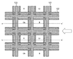
次に、第1の波長が第2の波長より短い例として第1実施例を挙げる。本発明の第1実施例に係る撮像装置について、図3を用いて説明する。図3は、本発明の第1実施例に係る撮像装置のレイアウト構成を示す図である。
R・gr=B・gb・・・数式1
となる。
(R+Gr・ar)・gr>(B+Gb・ab)・gb・・・数式2
となる。G画素の出力が一定として、Gr=Gbと考えると、明らかにRとBとは最終段で光学混色の強度に想定外の差が現れてしまう。
(第2実施例)
次に、本発明の第2実施例について説明する。
(第3実施例)
次に、本発明の第3実施例について、図6を用いて説明する。図6は、本発明の第3実施例に係る撮像装置のレイアウト構成を示す図である。
(第4実施例)
次に、本発明の第4実施例について、図7を用いて説明する。図7は、本発明の第4実施例に係る撮像装置のレイアウト構成を示す図である。
(第5実施例)
次に、本発明の第5実施例について、図8を用いて説明する。図8は、本発明の第5実施例に係る撮像装置の断面構成を示す図である。図8は、図7のa−a’の断面図に相当する。
(第6実施例)
次に、本発明の第6実施例について、図9及び図10を用いて説明する。図9は、本発明の第6実施例に係る撮像装置の設計途中におけるレイアウト構成を示す図である。図10は、本発明の第6実施例に係る撮像装置のレイアウト構成を示す図である。
100 撮像装置
Claims (2)
- ベイヤー配列に従うカラーフィルタ配列と、前記カラーフィルタ配列によって定められる青色画素、緑色画素および赤色画素が配列された画素配列と、前記カラーフィルタ配列と前記画素配列との間に設けられ、青色画素、緑色画素および赤色画素のそれぞれの開口領域を規定する配線層と、を備えた撮像装置であって、
前記画素配列は、所定方向に沿って青色画素と緑色画素とが交互に配された第1画素群と、前記所定方向に沿って赤色画素と緑色画素とが交互に配された第2画素群と、を有し、
前記第1画素群における青色画素および緑色画素のための開口領域が、前記第2画素群における赤色画素および緑色画素のための開口領域よりも大きい、
ことを特徴とする撮像装置。 - 請求項1に記載の撮像装置と、
前記撮像装置の撮像面へ像を形成する光学系と、
前記撮像装置から出力された信号を処理して画像データを生成する信号処理部と、を備え、
前記撮像装置は、被写体を撮影する前に、基準白色物体を撮像し、
前記信号処理部は、表示用又は記録用の画像における前記基準白色物体の適正な白レベルが得られるように、青色画素から出力された信号に対するゲインを赤色画素から出力された信号に対するゲインより小さな値に決定することを特徴とする撮像システム。
Priority Applications (4)
| Application Number | Priority Date | Filing Date | Title |
|---|---|---|---|
| JP2008051120A JP5173493B2 (ja) | 2008-02-29 | 2008-02-29 | 撮像装置及び撮像システム |
| US12/372,099 US8106343B2 (en) | 2008-02-29 | 2009-02-17 | Image sensing system interposing light shielding portion between color filter and pixel arrays |
| US13/350,273 US20120105670A1 (en) | 2008-02-29 | 2012-01-13 | Image sensing apparatus and imaging system |
| US14/150,425 US20140117211A1 (en) | 2008-02-29 | 2014-01-08 | Image sensing apparatus and imaging system |
Applications Claiming Priority (1)
| Application Number | Priority Date | Filing Date | Title |
|---|---|---|---|
| JP2008051120A JP5173493B2 (ja) | 2008-02-29 | 2008-02-29 | 撮像装置及び撮像システム |
Publications (3)
| Publication Number | Publication Date |
|---|---|
| JP2009212154A JP2009212154A (ja) | 2009-09-17 |
| JP2009212154A5 JP2009212154A5 (ja) | 2011-04-14 |
| JP5173493B2 true JP5173493B2 (ja) | 2013-04-03 |
Family
ID=41012447
Family Applications (1)
| Application Number | Title | Priority Date | Filing Date |
|---|---|---|---|
| JP2008051120A Expired - Fee Related JP5173493B2 (ja) | 2008-02-29 | 2008-02-29 | 撮像装置及び撮像システム |
Country Status (2)
| Country | Link |
|---|---|
| US (3) | US8106343B2 (ja) |
| JP (1) | JP5173493B2 (ja) |
Families Citing this family (36)
| Publication number | Priority date | Publication date | Assignee | Title |
|---|---|---|---|---|
| JP5173493B2 (ja) * | 2008-02-29 | 2013-04-03 | キヤノン株式会社 | 撮像装置及び撮像システム |
| JP5274166B2 (ja) * | 2008-09-10 | 2013-08-28 | キヤノン株式会社 | 光電変換装置及び撮像システム |
| JP4978614B2 (ja) * | 2008-11-25 | 2012-07-18 | ソニー株式会社 | 固体撮像装置 |
| JP5529613B2 (ja) * | 2009-04-17 | 2014-06-25 | キヤノン株式会社 | 光電変換装置及び撮像システム |
| JP5539104B2 (ja) * | 2009-09-24 | 2014-07-02 | キヤノン株式会社 | 光電変換装置およびそれを用いた撮像システム |
| JP5539105B2 (ja) * | 2009-09-24 | 2014-07-02 | キヤノン株式会社 | 光電変換装置およびそれを用いた撮像システム |
| JP5679653B2 (ja) * | 2009-12-09 | 2015-03-04 | キヤノン株式会社 | 光電変換装置およびそれを用いた撮像システム |
| JP5814613B2 (ja) | 2010-05-21 | 2015-11-17 | キヤノン株式会社 | 固体撮像装置 |
| JP5643555B2 (ja) | 2010-07-07 | 2014-12-17 | キヤノン株式会社 | 固体撮像装置及び撮像システム |
| JP5645513B2 (ja) | 2010-07-07 | 2014-12-24 | キヤノン株式会社 | 固体撮像装置及び撮像システム |
| JP5697371B2 (ja) | 2010-07-07 | 2015-04-08 | キヤノン株式会社 | 固体撮像装置および撮像システム |
| JP5751766B2 (ja) | 2010-07-07 | 2015-07-22 | キヤノン株式会社 | 固体撮像装置および撮像システム |
| JP5885401B2 (ja) | 2010-07-07 | 2016-03-15 | キヤノン株式会社 | 固体撮像装置および撮像システム |
| JP5656484B2 (ja) | 2010-07-07 | 2015-01-21 | キヤノン株式会社 | 固体撮像装置および撮像システム |
| JP5763474B2 (ja) * | 2010-08-27 | 2015-08-12 | 株式会社半導体エネルギー研究所 | 光センサ |
| JP6053505B2 (ja) | 2012-01-18 | 2016-12-27 | キヤノン株式会社 | 固体撮像装置 |
| US9093351B2 (en) | 2012-03-21 | 2015-07-28 | Canon Kabushiki Kaisha | Solid-state imaging apparatus |
| JP5778873B2 (ja) * | 2012-12-07 | 2015-09-16 | 富士フイルム株式会社 | 画像処理装置、画像処理方法及びプログラム、並びに記録媒体 |
| JP2014165270A (ja) * | 2013-02-22 | 2014-09-08 | Sony Corp | イメージセンサおよび電子機器 |
| JP6209890B2 (ja) * | 2013-07-29 | 2017-10-11 | ソニー株式会社 | 裏面照射型イメージセンサ、撮像装置、および電子機器 |
| JP6274788B2 (ja) | 2013-08-28 | 2018-02-07 | キヤノン株式会社 | 撮像装置、撮像システム及び撮像装置の駆動方法 |
| JP2015146304A (ja) * | 2014-02-04 | 2015-08-13 | ソニー株式会社 | 表示装置、および電子機器 |
| JP2015192234A (ja) * | 2014-03-27 | 2015-11-02 | Hoya株式会社 | 撮像素子、測定装置、測定方法、及び撮像装置 |
| JP6482186B2 (ja) | 2014-05-23 | 2019-03-13 | キヤノン株式会社 | 撮像装置及びその駆動方法 |
| JP6351404B2 (ja) | 2014-07-02 | 2018-07-04 | キヤノン株式会社 | 撮像装置及び撮像システム |
| CN107004683B (zh) * | 2014-12-04 | 2020-10-16 | Jsr株式会社 | 固体摄像装置 |
| JP6480768B2 (ja) | 2015-03-17 | 2019-03-13 | キヤノン株式会社 | 固体撮像装置及びその駆動方法 |
| JP6558998B2 (ja) * | 2015-07-28 | 2019-08-14 | キヤノン株式会社 | 撮像装置 |
| JP6454447B2 (ja) | 2015-12-02 | 2019-01-16 | アーベーベー・シュバイツ・アーゲー | 半導体装置の製造方法 |
| US10319765B2 (en) | 2016-07-01 | 2019-06-11 | Canon Kabushiki Kaisha | Imaging device having an effective pixel region, an optical black region and a dummy region each with pixels including a photoelectric converter |
| JP6904772B2 (ja) | 2017-04-26 | 2021-07-21 | キヤノン株式会社 | 固体撮像装置及びその駆動方法 |
| KR102375989B1 (ko) * | 2017-08-10 | 2022-03-18 | 삼성전자주식회사 | 화소 사이의 신호 차이를 보상하는 이미지 센서 |
| JP7102161B2 (ja) | 2018-02-15 | 2022-07-19 | キヤノン株式会社 | 撮像装置、撮像システム、及び、移動体 |
| JP7245014B2 (ja) | 2018-09-10 | 2023-03-23 | キヤノン株式会社 | 固体撮像装置、撮像システム、および固体撮像装置の駆動方法 |
| JP7353752B2 (ja) | 2018-12-06 | 2023-10-02 | キヤノン株式会社 | 光電変換装置及び撮像システム |
| JP2023023220A (ja) | 2021-08-04 | 2023-02-16 | キヤノン株式会社 | 光電変換装置 |
Family Cites Families (32)
| Publication number | Priority date | Publication date | Assignee | Title |
|---|---|---|---|---|
| DE3501138A1 (de) * | 1984-01-18 | 1985-07-18 | Canon K.K., Tokio/Tokyo | Bildaufnahmevorrichtung |
| US4663669A (en) * | 1984-02-01 | 1987-05-05 | Canon Kabushiki Kaisha | Image sensing apparatus |
| US4985760A (en) * | 1987-10-09 | 1991-01-15 | Canon Kabushiki Kaisha | Color imager having varying filter aperture sizes to compensate for luminance differences between colors |
| JPH0310460A (ja) * | 1989-06-07 | 1991-01-18 | Fuji Xerox Co Ltd | 画像読取装置の位置調整方法および装置 |
| JPH09116127A (ja) * | 1995-10-24 | 1997-05-02 | Sony Corp | 固体撮像装置 |
| US6674470B1 (en) * | 1996-09-19 | 2004-01-06 | Kabushiki Kaisha Toshiba | MOS-type solid state imaging device with high sensitivity |
| US6956605B1 (en) * | 1998-08-05 | 2005-10-18 | Canon Kabushiki Kaisha | Image pickup apparatus |
| EP1458028B1 (en) * | 1999-12-02 | 2011-05-11 | Nikon Corporation | Solid-state image sensor and production method of the same |
| US6646246B1 (en) * | 2000-11-21 | 2003-11-11 | Eastman Kodak Company | Method and system of noise removal for a sparsely sampled extended dynamic range image sensing device |
| US7742088B2 (en) * | 2002-11-19 | 2010-06-22 | Fujifilm Corporation | Image sensor and digital camera |
| JP4514188B2 (ja) * | 2003-11-10 | 2010-07-28 | キヤノン株式会社 | 光電変換装置及び撮像装置 |
| JP4508619B2 (ja) * | 2003-12-03 | 2010-07-21 | キヤノン株式会社 | 固体撮像装置の製造方法 |
| JP3793202B2 (ja) * | 2004-02-02 | 2006-07-05 | キヤノン株式会社 | 固体撮像装置 |
| JP3890333B2 (ja) * | 2004-02-06 | 2007-03-07 | キヤノン株式会社 | 固体撮像装置 |
| JP4067054B2 (ja) * | 2004-02-13 | 2008-03-26 | キヤノン株式会社 | 固体撮像装置および撮像システム |
| WO2005081020A1 (ja) * | 2004-02-19 | 2005-09-01 | Canon Kabushiki Kaisha | 光学機器およびビームスプリッター |
| JP4449565B2 (ja) * | 2004-05-12 | 2010-04-14 | ソニー株式会社 | 物理量分布検知の半導体装置 |
| US7605415B2 (en) * | 2004-06-07 | 2009-10-20 | Canon Kabushiki Kaisha | Image pickup device comprising photoelectric conversation unit, floating diffusion region and guard ring |
| JP4455435B2 (ja) * | 2004-08-04 | 2010-04-21 | キヤノン株式会社 | 固体撮像装置及び同固体撮像装置を用いたカメラ |
| JP5089017B2 (ja) * | 2004-09-01 | 2012-12-05 | キヤノン株式会社 | 固体撮像装置及び固体撮像システム |
| JP4916101B2 (ja) | 2004-09-01 | 2012-04-11 | キヤノン株式会社 | 光電変換装置、固体撮像装置及び固体撮像システム |
| JP4971586B2 (ja) * | 2004-09-01 | 2012-07-11 | キヤノン株式会社 | 固体撮像装置 |
| JP2006073736A (ja) | 2004-09-01 | 2006-03-16 | Canon Inc | 光電変換装置、固体撮像装置及び固体撮像システム |
| JP4434991B2 (ja) * | 2005-03-01 | 2010-03-17 | キヤノン株式会社 | イメージセンサ |
| JP5005179B2 (ja) * | 2005-03-23 | 2012-08-22 | ソニー株式会社 | 固体撮像装置 |
| US7791158B2 (en) * | 2005-04-13 | 2010-09-07 | Samsung Electronics Co., Ltd. | CMOS image sensor including an interlayer insulating layer and method of manufacturing the same |
| JP2007005629A (ja) | 2005-06-24 | 2007-01-11 | Matsushita Electric Ind Co Ltd | 固体撮像装置 |
| US7683407B2 (en) * | 2005-08-01 | 2010-03-23 | Aptina Imaging Corporation | Structure and method for building a light tunnel for use with imaging devices |
| JP5123601B2 (ja) * | 2006-08-31 | 2013-01-23 | キヤノン株式会社 | 光電変換装置 |
| JP4928199B2 (ja) * | 2006-09-07 | 2012-05-09 | キヤノン株式会社 | 信号検出装置、信号検出装置の信号読み出し方法及び信号検出装置を用いた撮像システム |
| JP5142696B2 (ja) * | 2007-12-20 | 2013-02-13 | キヤノン株式会社 | 光電変換装置、及び光電変換装置を用いた撮像システム |
| JP5173493B2 (ja) * | 2008-02-29 | 2013-04-03 | キヤノン株式会社 | 撮像装置及び撮像システム |
-
2008
- 2008-02-29 JP JP2008051120A patent/JP5173493B2/ja not_active Expired - Fee Related
-
2009
- 2009-02-17 US US12/372,099 patent/US8106343B2/en not_active Expired - Fee Related
-
2012
- 2012-01-13 US US13/350,273 patent/US20120105670A1/en not_active Abandoned
-
2014
- 2014-01-08 US US14/150,425 patent/US20140117211A1/en not_active Abandoned
Also Published As
| Publication number | Publication date |
|---|---|
| US20140117211A1 (en) | 2014-05-01 |
| US20120105670A1 (en) | 2012-05-03 |
| US8106343B2 (en) | 2012-01-31 |
| US20090218479A1 (en) | 2009-09-03 |
| JP2009212154A (ja) | 2009-09-17 |
Similar Documents
| Publication | Publication Date | Title |
|---|---|---|
| JP5173493B2 (ja) | 撮像装置及び撮像システム | |
| JP7264187B2 (ja) | 固体撮像装置およびその駆動方法、並びに電子機器 | |
| JP5089017B2 (ja) | 固体撮像装置及び固体撮像システム | |
| US9560325B2 (en) | Imaging device camera system and driving method of the same | |
| US7750278B2 (en) | Solid-state imaging device, method for driving solid-state imaging device and camera | |
| KR100818987B1 (ko) | 이미지 촬상 장치 및 상기 이미지 촬상 장치의 동작 방법 | |
| US9918027B2 (en) | Solid-state imaging device and electronic apparatus | |
| JP2011205348A (ja) | 固体撮像装置および画像記録装置 | |
| WO2021159944A1 (zh) | 图像传感器、摄像头组件及移动终端 | |
| US20220336508A1 (en) | Image sensor, camera assembly and mobile terminal | |
| JP2011166477A (ja) | 固体撮像素子及び画像入力装置 | |
| TWI416749B (zh) | 固態攝影裝置 | |
| JP2007235418A (ja) | 固体撮像装置 | |
| US9716867B2 (en) | Color filter array and image sensor having the same | |
| WO2021062661A1 (zh) | 图像传感器、摄像头组件及移动终端 | |
| JP2007066962A (ja) | カラー固体撮像装置及びデジタルカメラ | |
| JP2016019232A (ja) | 撮像素子及び撮像装置 | |
| CN114008781A (zh) | 图像传感器、摄像头组件及移动终端 | |
| JP2009049524A (ja) | 撮像装置及び信号処理方法 | |
| JP5619093B2 (ja) | 固体撮像装置及び固体撮像システム | |
| TWI795796B (zh) | 固體攝像裝置、固體攝像裝置的信號處理方法、以及電子機器 | |
| WO2021046690A1 (zh) | 图像传感器、摄像头模组、移动终端及图像采集方法 | |
| JP2024001490A (ja) | 固体撮像装置、固体撮像装置の製造方法、および電子機器 |
Legal Events
| Date | Code | Title | Description |
|---|---|---|---|
| A521 | Request for written amendment filed |
Free format text: JAPANESE INTERMEDIATE CODE: A523 Effective date: 20110228 |
|
| A621 | Written request for application examination |
Free format text: JAPANESE INTERMEDIATE CODE: A621 Effective date: 20110228 |
|
| A131 | Notification of reasons for refusal |
Free format text: JAPANESE INTERMEDIATE CODE: A131 Effective date: 20120910 |
|
| A521 | Request for written amendment filed |
Free format text: JAPANESE INTERMEDIATE CODE: A523 Effective date: 20121109 |
|
| TRDD | Decision of grant or rejection written | ||
| A01 | Written decision to grant a patent or to grant a registration (utility model) |
Free format text: JAPANESE INTERMEDIATE CODE: A01 Effective date: 20121207 |
|
| A61 | First payment of annual fees (during grant procedure) |
Free format text: JAPANESE INTERMEDIATE CODE: A61 Effective date: 20121227 |
|
| R151 | Written notification of patent or utility model registration |
Ref document number: 5173493 Country of ref document: JP Free format text: JAPANESE INTERMEDIATE CODE: R151 |
|
| FPAY | Renewal fee payment (event date is renewal date of database) |
Free format text: PAYMENT UNTIL: 20160111 Year of fee payment: 3 |
|
| LAPS | Cancellation because of no payment of annual fees |