EP1480270B1 - Dispositif d'emballage et boîtier semi-conducteur - Google Patents
Dispositif d'emballage et boîtier semi-conducteur Download PDFInfo
- Publication number
- EP1480270B1 EP1480270B1 EP04010184.2A EP04010184A EP1480270B1 EP 1480270 B1 EP1480270 B1 EP 1480270B1 EP 04010184 A EP04010184 A EP 04010184A EP 1480270 B1 EP1480270 B1 EP 1480270B1
- Authority
- EP
- European Patent Office
- Prior art keywords
- plated layer
- layer
- packaging component
- rough
- lead frame
- Prior art date
- Legal status (The legal status is an assumption and is not a legal conclusion. Google has not performed a legal analysis and makes no representation as to the accuracy of the status listed.)
- Expired - Lifetime
Links
- 239000004065 semiconductor Substances 0.000 title claims description 139
- 238000004806 packaging method and process Methods 0.000 title claims description 90
- 239000010410 layer Substances 0.000 claims description 282
- 239000011347 resin Substances 0.000 claims description 81
- 229920005989 resin Polymers 0.000 claims description 81
- PXHVJJICTQNCMI-UHFFFAOYSA-N Nickel Chemical compound [Ni] PXHVJJICTQNCMI-UHFFFAOYSA-N 0.000 claims description 72
- 238000007747 plating Methods 0.000 claims description 66
- 239000000758 substrate Substances 0.000 claims description 41
- 229910052802 copper Inorganic materials 0.000 claims description 39
- 239000010949 copper Substances 0.000 claims description 39
- RYGMFSIKBFXOCR-UHFFFAOYSA-N Copper Chemical compound [Cu] RYGMFSIKBFXOCR-UHFFFAOYSA-N 0.000 claims description 38
- 239000004020 conductor Substances 0.000 claims description 34
- 229910052751 metal Inorganic materials 0.000 claims description 30
- 239000002184 metal Substances 0.000 claims description 30
- 229910052759 nickel Inorganic materials 0.000 claims description 29
- KDLHZDBZIXYQEI-UHFFFAOYSA-N Palladium Chemical compound [Pd] KDLHZDBZIXYQEI-UHFFFAOYSA-N 0.000 claims description 24
- 229910045601 alloy Inorganic materials 0.000 claims description 20
- 239000000956 alloy Substances 0.000 claims description 20
- 239000010931 gold Substances 0.000 claims description 19
- 239000012790 adhesive layer Substances 0.000 claims description 17
- PCHJSUWPFVWCPO-UHFFFAOYSA-N gold Chemical compound [Au] PCHJSUWPFVWCPO-UHFFFAOYSA-N 0.000 claims description 12
- 229910052737 gold Inorganic materials 0.000 claims description 12
- 229910052763 palladium Inorganic materials 0.000 claims description 11
- BQCADISMDOOEFD-UHFFFAOYSA-N Silver Chemical compound [Ag] BQCADISMDOOEFD-UHFFFAOYSA-N 0.000 claims description 9
- 229910052709 silver Inorganic materials 0.000 claims description 9
- 239000004332 silver Substances 0.000 claims description 9
- ATJFFYVFTNAWJD-UHFFFAOYSA-N Tin Chemical compound [Sn] ATJFFYVFTNAWJD-UHFFFAOYSA-N 0.000 claims description 7
- 229910052718 tin Inorganic materials 0.000 claims description 7
- 239000011135 tin Substances 0.000 claims description 7
- VYZAMTAEIAYCRO-UHFFFAOYSA-N Chromium Chemical compound [Cr] VYZAMTAEIAYCRO-UHFFFAOYSA-N 0.000 claims description 6
- 229910052782 aluminium Inorganic materials 0.000 claims description 6
- XAGFODPZIPBFFR-UHFFFAOYSA-N aluminium Chemical compound [Al] XAGFODPZIPBFFR-UHFFFAOYSA-N 0.000 claims description 6
- 229910052804 chromium Inorganic materials 0.000 claims description 6
- 239000011651 chromium Substances 0.000 claims description 6
- 230000001590 oxidative effect Effects 0.000 claims description 6
- 150000001875 compounds Chemical class 0.000 claims description 5
- UGKDIUIOSMUOAW-UHFFFAOYSA-N iron nickel Chemical compound [Fe].[Ni] UGKDIUIOSMUOAW-UHFFFAOYSA-N 0.000 claims description 3
- 150000002739 metals Chemical class 0.000 claims description 3
- 238000000034 method Methods 0.000 description 49
- 238000007789 sealing Methods 0.000 description 47
- 239000010408 film Substances 0.000 description 20
- 238000001878 scanning electron micrograph Methods 0.000 description 16
- 231100000241 scar Toxicity 0.000 description 15
- 229910000881 Cu alloy Inorganic materials 0.000 description 11
- 239000002344 surface layer Substances 0.000 description 11
- 230000000694 effects Effects 0.000 description 10
- 238000009713 electroplating Methods 0.000 description 10
- 208000032544 Cicatrix Diseases 0.000 description 9
- 238000005259 measurement Methods 0.000 description 9
- 230000037387 scars Effects 0.000 description 9
- 230000015572 biosynthetic process Effects 0.000 description 8
- 238000010586 diagram Methods 0.000 description 8
- BASFCYQUMIYNBI-UHFFFAOYSA-N platinum Chemical compound [Pt] BASFCYQUMIYNBI-UHFFFAOYSA-N 0.000 description 8
- 238000005211 surface analysis Methods 0.000 description 8
- 230000003746 surface roughness Effects 0.000 description 8
- 229910021586 Nickel(II) chloride Inorganic materials 0.000 description 6
- HEMHJVSKTPXQMS-UHFFFAOYSA-M Sodium hydroxide Chemical compound [OH-].[Na+] HEMHJVSKTPXQMS-UHFFFAOYSA-M 0.000 description 6
- 239000000463 material Substances 0.000 description 6
- 239000000203 mixture Substances 0.000 description 6
- QMMRZOWCJAIUJA-UHFFFAOYSA-L nickel dichloride Chemical compound Cl[Ni]Cl QMMRZOWCJAIUJA-UHFFFAOYSA-L 0.000 description 6
- QPLDLSVMHZLSFG-UHFFFAOYSA-N Copper oxide Chemical compound [Cu]=O QPLDLSVMHZLSFG-UHFFFAOYSA-N 0.000 description 5
- 230000007547 defect Effects 0.000 description 5
- 230000002542 deteriorative effect Effects 0.000 description 5
- 238000004519 manufacturing process Methods 0.000 description 5
- KERTUBUCQCSNJU-UHFFFAOYSA-L nickel(2+);disulfamate Chemical compound [Ni+2].NS([O-])(=O)=O.NS([O-])(=O)=O KERTUBUCQCSNJU-UHFFFAOYSA-L 0.000 description 5
- NLXLAEXVIDQMFP-UHFFFAOYSA-N Ammonia chloride Chemical compound [NH4+].[Cl-] NLXLAEXVIDQMFP-UHFFFAOYSA-N 0.000 description 4
- XEEYBQQBJWHFJM-UHFFFAOYSA-N Iron Chemical compound [Fe] XEEYBQQBJWHFJM-UHFFFAOYSA-N 0.000 description 4
- 229910000990 Ni alloy Inorganic materials 0.000 description 4
- 238000005299 abrasion Methods 0.000 description 4
- 239000000853 adhesive Substances 0.000 description 4
- 230000032683 aging Effects 0.000 description 4
- 238000004873 anchoring Methods 0.000 description 4
- 230000006866 deterioration Effects 0.000 description 4
- 238000001000 micrograph Methods 0.000 description 4
- 229910052697 platinum Inorganic materials 0.000 description 4
- 238000010008 shearing Methods 0.000 description 4
- 239000002356 single layer Substances 0.000 description 4
- 229910000679 solder Inorganic materials 0.000 description 4
- 229910021585 Nickel(II) bromide Inorganic materials 0.000 description 3
- 230000001070 adhesive effect Effects 0.000 description 3
- 230000008859 change Effects 0.000 description 3
- IPLJNQFXJUCRNH-UHFFFAOYSA-L nickel(2+);dibromide Chemical compound [Ni+2].[Br-].[Br-] IPLJNQFXJUCRNH-UHFFFAOYSA-L 0.000 description 3
- 229910001030 Iron–nickel alloy Inorganic materials 0.000 description 2
- 229910001252 Pd alloy Inorganic materials 0.000 description 2
- 239000002390 adhesive tape Substances 0.000 description 2
- 235000019270 ammonium chloride Nutrition 0.000 description 2
- KGBXLFKZBHKPEV-UHFFFAOYSA-N boric acid Chemical compound OB(O)O KGBXLFKZBHKPEV-UHFFFAOYSA-N 0.000 description 2
- 239000004327 boric acid Substances 0.000 description 2
- 238000004364 calculation method Methods 0.000 description 2
- 239000013078 crystal Substances 0.000 description 2
- 229960004643 cupric oxide Drugs 0.000 description 2
- 239000006185 dispersion Substances 0.000 description 2
- 238000005469 granulation Methods 0.000 description 2
- 230000003179 granulation Effects 0.000 description 2
- 230000004048 modification Effects 0.000 description 2
- 238000012986 modification Methods 0.000 description 2
- 238000000465 moulding Methods 0.000 description 2
- 230000003647 oxidation Effects 0.000 description 2
- 238000007254 oxidation reaction Methods 0.000 description 2
- 229920001721 polyimide Polymers 0.000 description 2
- 238000002360 preparation method Methods 0.000 description 2
- 230000008569 process Effects 0.000 description 2
- UKLNMMHNWFDKNT-UHFFFAOYSA-M sodium chlorite Chemical compound [Na+].[O-]Cl=O UKLNMMHNWFDKNT-UHFFFAOYSA-M 0.000 description 2
- VGTPCRGMBIAPIM-UHFFFAOYSA-M sodium thiocyanate Chemical compound [Na+].[S-]C#N VGTPCRGMBIAPIM-UHFFFAOYSA-M 0.000 description 2
- 239000007858 starting material Substances 0.000 description 2
- RYFMWSXOAZQYPI-UHFFFAOYSA-K trisodium phosphate Chemical compound [Na+].[Na+].[Na+].[O-]P([O-])([O-])=O RYFMWSXOAZQYPI-UHFFFAOYSA-K 0.000 description 2
- 229910000406 trisodium phosphate Inorganic materials 0.000 description 2
- 235000019801 trisodium phosphate Nutrition 0.000 description 2
- 229910001316 Ag alloy Inorganic materials 0.000 description 1
- 229910001020 Au alloy Inorganic materials 0.000 description 1
- 239000005751 Copper oxide Substances 0.000 description 1
- 229910000640 Fe alloy Inorganic materials 0.000 description 1
- 229910003271 Ni-Fe Inorganic materials 0.000 description 1
- VEQPNABPJHWNSG-UHFFFAOYSA-N Nickel(2+) Chemical compound [Ni+2] VEQPNABPJHWNSG-UHFFFAOYSA-N 0.000 description 1
- 239000004642 Polyimide Substances 0.000 description 1
- BZHJMEDXRYGGRV-UHFFFAOYSA-N Vinyl chloride Chemical compound ClC=C BZHJMEDXRYGGRV-UHFFFAOYSA-N 0.000 description 1
- HCHKCACWOHOZIP-UHFFFAOYSA-N Zinc Chemical compound [Zn] HCHKCACWOHOZIP-UHFFFAOYSA-N 0.000 description 1
- UVTGXFAWNQTDBG-UHFFFAOYSA-N [Fe].[Pb] Chemical compound [Fe].[Pb] UVTGXFAWNQTDBG-UHFFFAOYSA-N 0.000 description 1
- 230000009471 action Effects 0.000 description 1
- 239000003513 alkali Substances 0.000 description 1
- 238000007743 anodising Methods 0.000 description 1
- 238000001311 chemical methods and process Methods 0.000 description 1
- 238000006243 chemical reaction Methods 0.000 description 1
- 238000010276 construction Methods 0.000 description 1
- 238000007796 conventional method Methods 0.000 description 1
- 229910000431 copper oxide Inorganic materials 0.000 description 1
- 230000007797 corrosion Effects 0.000 description 1
- 238000005260 corrosion Methods 0.000 description 1
- 238000005520 cutting process Methods 0.000 description 1
- 230000003247 decreasing effect Effects 0.000 description 1
- 230000032798 delamination Effects 0.000 description 1
- 238000000635 electron micrograph Methods 0.000 description 1
- 238000005516 engineering process Methods 0.000 description 1
- 239000003822 epoxy resin Substances 0.000 description 1
- 238000005530 etching Methods 0.000 description 1
- 210000003746 feather Anatomy 0.000 description 1
- 239000011521 glass Substances 0.000 description 1
- 239000003353 gold alloy Substances 0.000 description 1
- 238000010438 heat treatment Methods 0.000 description 1
- 239000011796 hollow space material Substances 0.000 description 1
- 238000010330 laser marking Methods 0.000 description 1
- 238000003754 machining Methods 0.000 description 1
- 239000007769 metal material Substances 0.000 description 1
- 229910001453 nickel ion Inorganic materials 0.000 description 1
- 229910000510 noble metal Inorganic materials 0.000 description 1
- 239000007800 oxidant agent Substances 0.000 description 1
- 239000002245 particle Substances 0.000 description 1
- 239000005011 phenolic resin Substances 0.000 description 1
- 229920000647 polyepoxide Polymers 0.000 description 1
- 239000009719 polyimide resin Substances 0.000 description 1
- 239000002243 precursor Substances 0.000 description 1
- 230000002265 prevention Effects 0.000 description 1
- 230000005855 radiation Effects 0.000 description 1
- 238000007788 roughening Methods 0.000 description 1
- 238000006748 scratching Methods 0.000 description 1
- 230000002393 scratching effect Effects 0.000 description 1
- 230000035939 shock Effects 0.000 description 1
- 229960002218 sodium chlorite Drugs 0.000 description 1
- 239000001488 sodium phosphate Substances 0.000 description 1
- 238000004544 sputter deposition Methods 0.000 description 1
- 230000035882 stress Effects 0.000 description 1
- 239000000126 substance Substances 0.000 description 1
- 238000004381 surface treatment Methods 0.000 description 1
- 239000000057 synthetic resin Substances 0.000 description 1
- 229920003002 synthetic resin Polymers 0.000 description 1
- 238000012360 testing method Methods 0.000 description 1
- 239000010409 thin film Substances 0.000 description 1
- 238000007738 vacuum evaporation Methods 0.000 description 1
- 239000002023 wood Substances 0.000 description 1
- 229910052725 zinc Inorganic materials 0.000 description 1
- 239000011701 zinc Substances 0.000 description 1
Images


Classifications
-
- H—ELECTRICITY
- H01—ELECTRIC ELEMENTS
- H01L—SEMICONDUCTOR DEVICES NOT COVERED BY CLASS H10
- H01L23/00—Details of semiconductor or other solid state devices
- H01L23/48—Arrangements for conducting electric current to or from the solid state body in operation, e.g. leads, terminal arrangements ; Selection of materials therefor
- H01L23/488—Arrangements for conducting electric current to or from the solid state body in operation, e.g. leads, terminal arrangements ; Selection of materials therefor consisting of soldered or bonded constructions
- H01L23/495—Lead-frames or other flat leads
- H01L23/49579—Lead-frames or other flat leads characterised by the materials of the lead frames or layers thereon
- H01L23/49582—Metallic layers on lead frames
-
- A—HUMAN NECESSITIES
- A47—FURNITURE; DOMESTIC ARTICLES OR APPLIANCES; COFFEE MILLS; SPICE MILLS; SUCTION CLEANERS IN GENERAL
- A47J—KITCHEN EQUIPMENT; COFFEE MILLS; SPICE MILLS; APPARATUS FOR MAKING BEVERAGES
- A47J27/00—Cooking-vessels
- A47J27/12—Multiple-unit cooking vessels
- A47J27/13—Tier cooking-vessels
-
- C—CHEMISTRY; METALLURGY
- C25—ELECTROLYTIC OR ELECTROPHORETIC PROCESSES; APPARATUS THEREFOR
- C25D—PROCESSES FOR THE ELECTROLYTIC OR ELECTROPHORETIC PRODUCTION OF COATINGS; ELECTROFORMING; APPARATUS THEREFOR
- C25D5/00—Electroplating characterised by the process; Pretreatment or after-treatment of workpieces
- C25D5/02—Electroplating of selected surface areas
-
- C—CHEMISTRY; METALLURGY
- C25—ELECTROLYTIC OR ELECTROPHORETIC PROCESSES; APPARATUS THEREFOR
- C25D—PROCESSES FOR THE ELECTROLYTIC OR ELECTROPHORETIC PRODUCTION OF COATINGS; ELECTROFORMING; APPARATUS THEREFOR
- C25D5/00—Electroplating characterised by the process; Pretreatment or after-treatment of workpieces
- C25D5/10—Electroplating with more than one layer of the same or of different metals
- C25D5/12—Electroplating with more than one layer of the same or of different metals at least one layer being of nickel or chromium
-
- C—CHEMISTRY; METALLURGY
- C25—ELECTROLYTIC OR ELECTROPHORETIC PROCESSES; APPARATUS THEREFOR
- C25D—PROCESSES FOR THE ELECTROLYTIC OR ELECTROPHORETIC PRODUCTION OF COATINGS; ELECTROFORMING; APPARATUS THEREFOR
- C25D5/00—Electroplating characterised by the process; Pretreatment or after-treatment of workpieces
- C25D5/60—Electroplating characterised by the structure or texture of the layers
- C25D5/605—Surface topography of the layers, e.g. rough, dendritic or nodular layers
- C25D5/611—Smooth layers
-
- C—CHEMISTRY; METALLURGY
- C25—ELECTROLYTIC OR ELECTROPHORETIC PROCESSES; APPARATUS THEREFOR
- C25D—PROCESSES FOR THE ELECTROLYTIC OR ELECTROPHORETIC PRODUCTION OF COATINGS; ELECTROFORMING; APPARATUS THEREFOR
- C25D5/00—Electroplating characterised by the process; Pretreatment or after-treatment of workpieces
- C25D5/60—Electroplating characterised by the structure or texture of the layers
- C25D5/615—Microstructure of the layers, e.g. mixed structure
- C25D5/617—Crystalline layers
-
- C—CHEMISTRY; METALLURGY
- C25—ELECTROLYTIC OR ELECTROPHORETIC PROCESSES; APPARATUS THEREFOR
- C25D—PROCESSES FOR THE ELECTROLYTIC OR ELECTROPHORETIC PRODUCTION OF COATINGS; ELECTROFORMING; APPARATUS THEREFOR
- C25D5/00—Electroplating characterised by the process; Pretreatment or after-treatment of workpieces
- C25D5/627—Electroplating characterised by the visual appearance of the layers, e.g. colour, brightness or mat appearance
-
- H—ELECTRICITY
- H01—ELECTRIC ELEMENTS
- H01L—SEMICONDUCTOR DEVICES NOT COVERED BY CLASS H10
- H01L24/00—Arrangements for connecting or disconnecting semiconductor or solid-state bodies; Methods or apparatus related thereto
- H01L24/01—Means for bonding being attached to, or being formed on, the surface to be connected, e.g. chip-to-package, die-attach, "first-level" interconnects; Manufacturing methods related thereto
- H01L24/42—Wire connectors; Manufacturing methods related thereto
- H01L24/47—Structure, shape, material or disposition of the wire connectors after the connecting process
- H01L24/48—Structure, shape, material or disposition of the wire connectors after the connecting process of an individual wire connector
-
- H—ELECTRICITY
- H05—ELECTRIC TECHNIQUES NOT OTHERWISE PROVIDED FOR
- H05B—ELECTRIC HEATING; ELECTRIC LIGHT SOURCES NOT OTHERWISE PROVIDED FOR; CIRCUIT ARRANGEMENTS FOR ELECTRIC LIGHT SOURCES, IN GENERAL
- H05B6/00—Heating by electric, magnetic or electromagnetic fields
- H05B6/64—Heating using microwaves
- H05B6/6408—Supports or covers specially adapted for use in microwave heating apparatus
-
- H—ELECTRICITY
- H01—ELECTRIC ELEMENTS
- H01L—SEMICONDUCTOR DEVICES NOT COVERED BY CLASS H10
- H01L2224/00—Indexing scheme for arrangements for connecting or disconnecting semiconductor or solid-state bodies and methods related thereto as covered by H01L24/00
- H01L2224/01—Means for bonding being attached to, or being formed on, the surface to be connected, e.g. chip-to-package, die-attach, "first-level" interconnects; Manufacturing methods related thereto
- H01L2224/10—Bump connectors; Manufacturing methods related thereto
- H01L2224/15—Structure, shape, material or disposition of the bump connectors after the connecting process
- H01L2224/16—Structure, shape, material or disposition of the bump connectors after the connecting process of an individual bump connector
-
- H—ELECTRICITY
- H01—ELECTRIC ELEMENTS
- H01L—SEMICONDUCTOR DEVICES NOT COVERED BY CLASS H10
- H01L2224/00—Indexing scheme for arrangements for connecting or disconnecting semiconductor or solid-state bodies and methods related thereto as covered by H01L24/00
- H01L2224/01—Means for bonding being attached to, or being formed on, the surface to be connected, e.g. chip-to-package, die-attach, "first-level" interconnects; Manufacturing methods related thereto
- H01L2224/42—Wire connectors; Manufacturing methods related thereto
- H01L2224/44—Structure, shape, material or disposition of the wire connectors prior to the connecting process
- H01L2224/45—Structure, shape, material or disposition of the wire connectors prior to the connecting process of an individual wire connector
- H01L2224/45001—Core members of the connector
- H01L2224/45099—Material
- H01L2224/451—Material with a principal constituent of the material being a metal or a metalloid, e.g. boron (B), silicon (Si), germanium (Ge), arsenic (As), antimony (Sb), tellurium (Te) and polonium (Po), and alloys thereof
- H01L2224/45138—Material with a principal constituent of the material being a metal or a metalloid, e.g. boron (B), silicon (Si), germanium (Ge), arsenic (As), antimony (Sb), tellurium (Te) and polonium (Po), and alloys thereof the principal constituent melting at a temperature of greater than or equal to 950°C and less than 1550°C
- H01L2224/45144—Gold (Au) as principal constituent
-
- H—ELECTRICITY
- H01—ELECTRIC ELEMENTS
- H01L—SEMICONDUCTOR DEVICES NOT COVERED BY CLASS H10
- H01L2224/00—Indexing scheme for arrangements for connecting or disconnecting semiconductor or solid-state bodies and methods related thereto as covered by H01L24/00
- H01L2224/01—Means for bonding being attached to, or being formed on, the surface to be connected, e.g. chip-to-package, die-attach, "first-level" interconnects; Manufacturing methods related thereto
- H01L2224/42—Wire connectors; Manufacturing methods related thereto
- H01L2224/47—Structure, shape, material or disposition of the wire connectors after the connecting process
- H01L2224/48—Structure, shape, material or disposition of the wire connectors after the connecting process of an individual wire connector
- H01L2224/4805—Shape
- H01L2224/4809—Loop shape
- H01L2224/48091—Arched
-
- H—ELECTRICITY
- H01—ELECTRIC ELEMENTS
- H01L—SEMICONDUCTOR DEVICES NOT COVERED BY CLASS H10
- H01L2224/00—Indexing scheme for arrangements for connecting or disconnecting semiconductor or solid-state bodies and methods related thereto as covered by H01L24/00
- H01L2224/01—Means for bonding being attached to, or being formed on, the surface to be connected, e.g. chip-to-package, die-attach, "first-level" interconnects; Manufacturing methods related thereto
- H01L2224/42—Wire connectors; Manufacturing methods related thereto
- H01L2224/47—Structure, shape, material or disposition of the wire connectors after the connecting process
- H01L2224/48—Structure, shape, material or disposition of the wire connectors after the connecting process of an individual wire connector
- H01L2224/481—Disposition
- H01L2224/48151—Connecting between a semiconductor or solid-state body and an item not being a semiconductor or solid-state body, e.g. chip-to-substrate, chip-to-passive
- H01L2224/48221—Connecting between a semiconductor or solid-state body and an item not being a semiconductor or solid-state body, e.g. chip-to-substrate, chip-to-passive the body and the item being stacked
- H01L2224/48245—Connecting between a semiconductor or solid-state body and an item not being a semiconductor or solid-state body, e.g. chip-to-substrate, chip-to-passive the body and the item being stacked the item being metallic
- H01L2224/48247—Connecting between a semiconductor or solid-state body and an item not being a semiconductor or solid-state body, e.g. chip-to-substrate, chip-to-passive the body and the item being stacked the item being metallic connecting the wire to a bond pad of the item
-
- H—ELECTRICITY
- H01—ELECTRIC ELEMENTS
- H01L—SEMICONDUCTOR DEVICES NOT COVERED BY CLASS H10
- H01L2224/00—Indexing scheme for arrangements for connecting or disconnecting semiconductor or solid-state bodies and methods related thereto as covered by H01L24/00
- H01L2224/01—Means for bonding being attached to, or being formed on, the surface to be connected, e.g. chip-to-package, die-attach, "first-level" interconnects; Manufacturing methods related thereto
- H01L2224/42—Wire connectors; Manufacturing methods related thereto
- H01L2224/47—Structure, shape, material or disposition of the wire connectors after the connecting process
- H01L2224/48—Structure, shape, material or disposition of the wire connectors after the connecting process of an individual wire connector
- H01L2224/484—Connecting portions
-
- H—ELECTRICITY
- H01—ELECTRIC ELEMENTS
- H01L—SEMICONDUCTOR DEVICES NOT COVERED BY CLASS H10
- H01L2224/00—Indexing scheme for arrangements for connecting or disconnecting semiconductor or solid-state bodies and methods related thereto as covered by H01L24/00
- H01L2224/01—Means for bonding being attached to, or being formed on, the surface to be connected, e.g. chip-to-package, die-attach, "first-level" interconnects; Manufacturing methods related thereto
- H01L2224/42—Wire connectors; Manufacturing methods related thereto
- H01L2224/47—Structure, shape, material or disposition of the wire connectors after the connecting process
- H01L2224/48—Structure, shape, material or disposition of the wire connectors after the connecting process of an individual wire connector
- H01L2224/485—Material
- H01L2224/48505—Material at the bonding interface
- H01L2224/48599—Principal constituent of the connecting portion of the wire connector being Gold (Au)
- H01L2224/486—Principal constituent of the connecting portion of the wire connector being Gold (Au) with a principal constituent of the bonding area being a metal or a metalloid, e.g. boron (B), silicon (Si), germanium (Ge), arsenic (As), antimony (Sb), tellurium (Te) and polonium (Po), and alloys thereof
- H01L2224/48638—Principal constituent of the connecting portion of the wire connector being Gold (Au) with a principal constituent of the bonding area being a metal or a metalloid, e.g. boron (B), silicon (Si), germanium (Ge), arsenic (As), antimony (Sb), tellurium (Te) and polonium (Po), and alloys thereof the principal constituent melting at a temperature of greater than or equal to 950°C and less than 1550°C
- H01L2224/48639—Silver (Ag) as principal constituent
-
- H—ELECTRICITY
- H01—ELECTRIC ELEMENTS
- H01L—SEMICONDUCTOR DEVICES NOT COVERED BY CLASS H10
- H01L2224/00—Indexing scheme for arrangements for connecting or disconnecting semiconductor or solid-state bodies and methods related thereto as covered by H01L24/00
- H01L2224/01—Means for bonding being attached to, or being formed on, the surface to be connected, e.g. chip-to-package, die-attach, "first-level" interconnects; Manufacturing methods related thereto
- H01L2224/42—Wire connectors; Manufacturing methods related thereto
- H01L2224/47—Structure, shape, material or disposition of the wire connectors after the connecting process
- H01L2224/48—Structure, shape, material or disposition of the wire connectors after the connecting process of an individual wire connector
- H01L2224/485—Material
- H01L2224/48505—Material at the bonding interface
- H01L2224/48599—Principal constituent of the connecting portion of the wire connector being Gold (Au)
- H01L2224/486—Principal constituent of the connecting portion of the wire connector being Gold (Au) with a principal constituent of the bonding area being a metal or a metalloid, e.g. boron (B), silicon (Si), germanium (Ge), arsenic (As), antimony (Sb), tellurium (Te) and polonium (Po), and alloys thereof
- H01L2224/48663—Principal constituent of the connecting portion of the wire connector being Gold (Au) with a principal constituent of the bonding area being a metal or a metalloid, e.g. boron (B), silicon (Si), germanium (Ge), arsenic (As), antimony (Sb), tellurium (Te) and polonium (Po), and alloys thereof the principal constituent melting at a temperature of greater than 1550°C
- H01L2224/48664—Palladium (Pd) as principal constituent
-
- H—ELECTRICITY
- H01—ELECTRIC ELEMENTS
- H01L—SEMICONDUCTOR DEVICES NOT COVERED BY CLASS H10
- H01L2224/00—Indexing scheme for arrangements for connecting or disconnecting semiconductor or solid-state bodies and methods related thereto as covered by H01L24/00
- H01L2224/73—Means for bonding being of different types provided for in two or more of groups H01L2224/10, H01L2224/18, H01L2224/26, H01L2224/34, H01L2224/42, H01L2224/50, H01L2224/63, H01L2224/71
- H01L2224/732—Location after the connecting process
- H01L2224/73201—Location after the connecting process on the same surface
- H01L2224/73203—Bump and layer connectors
- H01L2224/73204—Bump and layer connectors the bump connector being embedded into the layer connector
-
- H—ELECTRICITY
- H01—ELECTRIC ELEMENTS
- H01L—SEMICONDUCTOR DEVICES NOT COVERED BY CLASS H10
- H01L2224/00—Indexing scheme for arrangements for connecting or disconnecting semiconductor or solid-state bodies and methods related thereto as covered by H01L24/00
- H01L2224/73—Means for bonding being of different types provided for in two or more of groups H01L2224/10, H01L2224/18, H01L2224/26, H01L2224/34, H01L2224/42, H01L2224/50, H01L2224/63, H01L2224/71
- H01L2224/732—Location after the connecting process
- H01L2224/73251—Location after the connecting process on different surfaces
- H01L2224/73253—Bump and layer connectors
-
- H—ELECTRICITY
- H01—ELECTRIC ELEMENTS
- H01L—SEMICONDUCTOR DEVICES NOT COVERED BY CLASS H10
- H01L2224/00—Indexing scheme for arrangements for connecting or disconnecting semiconductor or solid-state bodies and methods related thereto as covered by H01L24/00
- H01L2224/80—Methods for connecting semiconductor or other solid state bodies using means for bonding being attached to, or being formed on, the surface to be connected
- H01L2224/85—Methods for connecting semiconductor or other solid state bodies using means for bonding being attached to, or being formed on, the surface to be connected using a wire connector
- H01L2224/8538—Bonding interfaces outside the semiconductor or solid-state body
- H01L2224/85399—Material
- H01L2224/854—Material with a principal constituent of the material being a metal or a metalloid, e.g. boron (B), silicon (Si), germanium (Ge), arsenic (As), antimony (Sb), tellurium (Te) and polonium (Po), and alloys thereof
- H01L2224/85438—Material with a principal constituent of the material being a metal or a metalloid, e.g. boron (B), silicon (Si), germanium (Ge), arsenic (As), antimony (Sb), tellurium (Te) and polonium (Po), and alloys thereof the principal constituent melting at a temperature of greater than or equal to 950°C and less than 1550°C
- H01L2224/85439—Silver (Ag) as principal constituent
-
- H—ELECTRICITY
- H01—ELECTRIC ELEMENTS
- H01L—SEMICONDUCTOR DEVICES NOT COVERED BY CLASS H10
- H01L2224/00—Indexing scheme for arrangements for connecting or disconnecting semiconductor or solid-state bodies and methods related thereto as covered by H01L24/00
- H01L2224/80—Methods for connecting semiconductor or other solid state bodies using means for bonding being attached to, or being formed on, the surface to be connected
- H01L2224/85—Methods for connecting semiconductor or other solid state bodies using means for bonding being attached to, or being formed on, the surface to be connected using a wire connector
- H01L2224/8538—Bonding interfaces outside the semiconductor or solid-state body
- H01L2224/85399—Material
- H01L2224/854—Material with a principal constituent of the material being a metal or a metalloid, e.g. boron (B), silicon (Si), germanium (Ge), arsenic (As), antimony (Sb), tellurium (Te) and polonium (Po), and alloys thereof
- H01L2224/85463—Material with a principal constituent of the material being a metal or a metalloid, e.g. boron (B), silicon (Si), germanium (Ge), arsenic (As), antimony (Sb), tellurium (Te) and polonium (Po), and alloys thereof the principal constituent melting at a temperature of greater than 1550°C
- H01L2224/85464—Palladium (Pd) as principal constituent
-
- H—ELECTRICITY
- H01—ELECTRIC ELEMENTS
- H01L—SEMICONDUCTOR DEVICES NOT COVERED BY CLASS H10
- H01L23/00—Details of semiconductor or other solid state devices
- H01L23/34—Arrangements for cooling, heating, ventilating or temperature compensation ; Temperature sensing arrangements
- H01L23/42—Fillings or auxiliary members in containers or encapsulations selected or arranged to facilitate heating or cooling
- H01L23/433—Auxiliary members in containers characterised by their shape, e.g. pistons
- H01L23/4334—Auxiliary members in encapsulations
-
- H—ELECTRICITY
- H01—ELECTRIC ELEMENTS
- H01L—SEMICONDUCTOR DEVICES NOT COVERED BY CLASS H10
- H01L24/00—Arrangements for connecting or disconnecting semiconductor or solid-state bodies; Methods or apparatus related thereto
- H01L24/01—Means for bonding being attached to, or being formed on, the surface to be connected, e.g. chip-to-package, die-attach, "first-level" interconnects; Manufacturing methods related thereto
- H01L24/42—Wire connectors; Manufacturing methods related thereto
- H01L24/44—Structure, shape, material or disposition of the wire connectors prior to the connecting process
- H01L24/45—Structure, shape, material or disposition of the wire connectors prior to the connecting process of an individual wire connector
-
- H—ELECTRICITY
- H01—ELECTRIC ELEMENTS
- H01L—SEMICONDUCTOR DEVICES NOT COVERED BY CLASS H10
- H01L2924/00—Indexing scheme for arrangements or methods for connecting or disconnecting semiconductor or solid-state bodies as covered by H01L24/00
- H01L2924/0001—Technical content checked by a classifier
- H01L2924/00014—Technical content checked by a classifier the subject-matter covered by the group, the symbol of which is combined with the symbol of this group, being disclosed without further technical details
-
- H—ELECTRICITY
- H01—ELECTRIC ELEMENTS
- H01L—SEMICONDUCTOR DEVICES NOT COVERED BY CLASS H10
- H01L2924/00—Indexing scheme for arrangements or methods for connecting or disconnecting semiconductor or solid-state bodies as covered by H01L24/00
- H01L2924/01—Chemical elements
- H01L2924/01004—Beryllium [Be]
-
- H—ELECTRICITY
- H01—ELECTRIC ELEMENTS
- H01L—SEMICONDUCTOR DEVICES NOT COVERED BY CLASS H10
- H01L2924/00—Indexing scheme for arrangements or methods for connecting or disconnecting semiconductor or solid-state bodies as covered by H01L24/00
- H01L2924/01—Chemical elements
- H01L2924/01005—Boron [B]
-
- H—ELECTRICITY
- H01—ELECTRIC ELEMENTS
- H01L—SEMICONDUCTOR DEVICES NOT COVERED BY CLASS H10
- H01L2924/00—Indexing scheme for arrangements or methods for connecting or disconnecting semiconductor or solid-state bodies as covered by H01L24/00
- H01L2924/01—Chemical elements
- H01L2924/01006—Carbon [C]
-
- H—ELECTRICITY
- H01—ELECTRIC ELEMENTS
- H01L—SEMICONDUCTOR DEVICES NOT COVERED BY CLASS H10
- H01L2924/00—Indexing scheme for arrangements or methods for connecting or disconnecting semiconductor or solid-state bodies as covered by H01L24/00
- H01L2924/01—Chemical elements
- H01L2924/01011—Sodium [Na]
-
- H—ELECTRICITY
- H01—ELECTRIC ELEMENTS
- H01L—SEMICONDUCTOR DEVICES NOT COVERED BY CLASS H10
- H01L2924/00—Indexing scheme for arrangements or methods for connecting or disconnecting semiconductor or solid-state bodies as covered by H01L24/00
- H01L2924/01—Chemical elements
- H01L2924/01013—Aluminum [Al]
-
- H—ELECTRICITY
- H01—ELECTRIC ELEMENTS
- H01L—SEMICONDUCTOR DEVICES NOT COVERED BY CLASS H10
- H01L2924/00—Indexing scheme for arrangements or methods for connecting or disconnecting semiconductor or solid-state bodies as covered by H01L24/00
- H01L2924/01—Chemical elements
- H01L2924/01015—Phosphorus [P]
-
- H—ELECTRICITY
- H01—ELECTRIC ELEMENTS
- H01L—SEMICONDUCTOR DEVICES NOT COVERED BY CLASS H10
- H01L2924/00—Indexing scheme for arrangements or methods for connecting or disconnecting semiconductor or solid-state bodies as covered by H01L24/00
- H01L2924/01—Chemical elements
- H01L2924/01023—Vanadium [V]
-
- H—ELECTRICITY
- H01—ELECTRIC ELEMENTS
- H01L—SEMICONDUCTOR DEVICES NOT COVERED BY CLASS H10
- H01L2924/00—Indexing scheme for arrangements or methods for connecting or disconnecting semiconductor or solid-state bodies as covered by H01L24/00
- H01L2924/01—Chemical elements
- H01L2924/01024—Chromium [Cr]
-
- H—ELECTRICITY
- H01—ELECTRIC ELEMENTS
- H01L—SEMICONDUCTOR DEVICES NOT COVERED BY CLASS H10
- H01L2924/00—Indexing scheme for arrangements or methods for connecting or disconnecting semiconductor or solid-state bodies as covered by H01L24/00
- H01L2924/01—Chemical elements
- H01L2924/01028—Nickel [Ni]
-
- H—ELECTRICITY
- H01—ELECTRIC ELEMENTS
- H01L—SEMICONDUCTOR DEVICES NOT COVERED BY CLASS H10
- H01L2924/00—Indexing scheme for arrangements or methods for connecting or disconnecting semiconductor or solid-state bodies as covered by H01L24/00
- H01L2924/01—Chemical elements
- H01L2924/01029—Copper [Cu]
-
- H—ELECTRICITY
- H01—ELECTRIC ELEMENTS
- H01L—SEMICONDUCTOR DEVICES NOT COVERED BY CLASS H10
- H01L2924/00—Indexing scheme for arrangements or methods for connecting or disconnecting semiconductor or solid-state bodies as covered by H01L24/00
- H01L2924/01—Chemical elements
- H01L2924/01047—Silver [Ag]
-
- H—ELECTRICITY
- H01—ELECTRIC ELEMENTS
- H01L—SEMICONDUCTOR DEVICES NOT COVERED BY CLASS H10
- H01L2924/00—Indexing scheme for arrangements or methods for connecting or disconnecting semiconductor or solid-state bodies as covered by H01L24/00
- H01L2924/01—Chemical elements
- H01L2924/0105—Tin [Sn]
-
- H—ELECTRICITY
- H01—ELECTRIC ELEMENTS
- H01L—SEMICONDUCTOR DEVICES NOT COVERED BY CLASS H10
- H01L2924/00—Indexing scheme for arrangements or methods for connecting or disconnecting semiconductor or solid-state bodies as covered by H01L24/00
- H01L2924/01—Chemical elements
- H01L2924/01078—Platinum [Pt]
-
- H—ELECTRICITY
- H01—ELECTRIC ELEMENTS
- H01L—SEMICONDUCTOR DEVICES NOT COVERED BY CLASS H10
- H01L2924/00—Indexing scheme for arrangements or methods for connecting or disconnecting semiconductor or solid-state bodies as covered by H01L24/00
- H01L2924/01—Chemical elements
- H01L2924/01079—Gold [Au]
-
- H—ELECTRICITY
- H01—ELECTRIC ELEMENTS
- H01L—SEMICONDUCTOR DEVICES NOT COVERED BY CLASS H10
- H01L2924/00—Indexing scheme for arrangements or methods for connecting or disconnecting semiconductor or solid-state bodies as covered by H01L24/00
- H01L2924/01—Chemical elements
- H01L2924/01084—Polonium [Po]
-
- H—ELECTRICITY
- H01—ELECTRIC ELEMENTS
- H01L—SEMICONDUCTOR DEVICES NOT COVERED BY CLASS H10
- H01L2924/00—Indexing scheme for arrangements or methods for connecting or disconnecting semiconductor or solid-state bodies as covered by H01L24/00
- H01L2924/01—Chemical elements
- H01L2924/01088—Radium [Ra]
-
- H—ELECTRICITY
- H01—ELECTRIC ELEMENTS
- H01L—SEMICONDUCTOR DEVICES NOT COVERED BY CLASS H10
- H01L2924/00—Indexing scheme for arrangements or methods for connecting or disconnecting semiconductor or solid-state bodies as covered by H01L24/00
- H01L2924/013—Alloys
- H01L2924/014—Solder alloys
-
- H—ELECTRICITY
- H01—ELECTRIC ELEMENTS
- H01L—SEMICONDUCTOR DEVICES NOT COVERED BY CLASS H10
- H01L2924/00—Indexing scheme for arrangements or methods for connecting or disconnecting semiconductor or solid-state bodies as covered by H01L24/00
- H01L2924/10—Details of semiconductor or other solid state devices to be connected
- H01L2924/11—Device type
- H01L2924/12—Passive devices, e.g. 2 terminal devices
- H01L2924/1204—Optical Diode
- H01L2924/12042—LASER
-
- H—ELECTRICITY
- H01—ELECTRIC ELEMENTS
- H01L—SEMICONDUCTOR DEVICES NOT COVERED BY CLASS H10
- H01L2924/00—Indexing scheme for arrangements or methods for connecting or disconnecting semiconductor or solid-state bodies as covered by H01L24/00
- H01L2924/10—Details of semiconductor or other solid state devices to be connected
- H01L2924/11—Device type
- H01L2924/14—Integrated circuits
-
- H—ELECTRICITY
- H01—ELECTRIC ELEMENTS
- H01L—SEMICONDUCTOR DEVICES NOT COVERED BY CLASS H10
- H01L2924/00—Indexing scheme for arrangements or methods for connecting or disconnecting semiconductor or solid-state bodies as covered by H01L24/00
- H01L2924/15—Details of package parts other than the semiconductor or other solid state devices to be connected
- H01L2924/151—Die mounting substrate
- H01L2924/153—Connection portion
- H01L2924/1531—Connection portion the connection portion being formed only on the surface of the substrate opposite to the die mounting surface
- H01L2924/15311—Connection portion the connection portion being formed only on the surface of the substrate opposite to the die mounting surface being a ball array, e.g. BGA
-
- H—ELECTRICITY
- H01—ELECTRIC ELEMENTS
- H01L—SEMICONDUCTOR DEVICES NOT COVERED BY CLASS H10
- H01L2924/00—Indexing scheme for arrangements or methods for connecting or disconnecting semiconductor or solid-state bodies as covered by H01L24/00
- H01L2924/15—Details of package parts other than the semiconductor or other solid state devices to be connected
- H01L2924/151—Die mounting substrate
- H01L2924/156—Material
- H01L2924/157—Material with a principal constituent of the material being a metal or a metalloid, e.g. boron [B], silicon [Si], germanium [Ge], arsenic [As], antimony [Sb], tellurium [Te] and polonium [Po], and alloys thereof
- H01L2924/15738—Material with a principal constituent of the material being a metal or a metalloid, e.g. boron [B], silicon [Si], germanium [Ge], arsenic [As], antimony [Sb], tellurium [Te] and polonium [Po], and alloys thereof the principal constituent melting at a temperature of greater than or equal to 950 C and less than 1550 C
- H01L2924/15747—Copper [Cu] as principal constituent
-
- H—ELECTRICITY
- H01—ELECTRIC ELEMENTS
- H01L—SEMICONDUCTOR DEVICES NOT COVERED BY CLASS H10
- H01L2924/00—Indexing scheme for arrangements or methods for connecting or disconnecting semiconductor or solid-state bodies as covered by H01L24/00
- H01L2924/15—Details of package parts other than the semiconductor or other solid state devices to be connected
- H01L2924/161—Cap
- H01L2924/1615—Shape
- H01L2924/16152—Cap comprising a cavity for hosting the device, e.g. U-shaped cap
-
- H—ELECTRICITY
- H01—ELECTRIC ELEMENTS
- H01L—SEMICONDUCTOR DEVICES NOT COVERED BY CLASS H10
- H01L2924/00—Indexing scheme for arrangements or methods for connecting or disconnecting semiconductor or solid-state bodies as covered by H01L24/00
- H01L2924/15—Details of package parts other than the semiconductor or other solid state devices to be connected
- H01L2924/181—Encapsulation
- H01L2924/183—Connection portion, e.g. seal
- H01L2924/18301—Connection portion, e.g. seal being an anchoring portion, i.e. mechanical interlocking between the encapsulation resin and another package part
-
- H—ELECTRICITY
- H01—ELECTRIC ELEMENTS
- H01L—SEMICONDUCTOR DEVICES NOT COVERED BY CLASS H10
- H01L2924/00—Indexing scheme for arrangements or methods for connecting or disconnecting semiconductor or solid-state bodies as covered by H01L24/00
- H01L2924/30—Technical effects
- H01L2924/301—Electrical effects
- H01L2924/3025—Electromagnetic shielding
Definitions
- the present invention relates to a packaging component and, more particularly, to a part and other elements for use in packaging.
- the packaging component is useful for the formation of packages having a structure obtained by mounting a semiconductor element or other elements on the packaging component and sealing the element-mounting portion with an insulating resin, and packages in which an adhesive layer is used as a bonding means.
- the packaging component includes, for example, a lead frame and a heat-radiating or -dissipating plate used in the production of an electronic device.
- the invention further relates to a semiconductor package equipped with the packaging component of the present invention and other packages.
- semiconductor packages mounting a semiconductor element such as an IC chip or an LSI chip on a substrate such as a lead frame, and one of them includes a resin-sealed semiconductor package in which a semiconductor element is mounted and a portion mounting the semiconductor element is sealed with an insulating resin.
- the semiconductor packages as produced are usually stored, and are offered to end users, as required. The end users mount the semiconductor packages on substrates such as wiring boards by reflowing a solder to complete the final electronic devices.
- the lead frame is usually made of copper or an alloy thereof and its surface is plated with nickel (Ni) to improve its corrosion resistance and heat resistance.
- Ni nickel
- An Ni-plated layer usually, has a dense and smooth crystalline structure.
- the Ni-plated layer has a low shearing strength at the interface, good adhesion cannot be maintained between the Ni-plated layer and the sealing resin.
- the adhesion between the Ni-plated layer and the sealing resin tends to deteriorate with time.
- the sealing resin can absorb the moisture in the air.
- the sealing resin can expand developing defects such as cracks and causing the semiconductor elements to be peeled.
- the moisture absorbed by the sealing resin is rapidly vaporized and expanded due to the heat in the solder reflowing step (a temperature of as high as about 180 to 260° C is used in this step) at the time of mounting the semiconductor package, producing a large stress in the sealing resin itself.
- the sealing resin peels off the lead frame.
- Such defects deteriorate the reliability of the semiconductor package. It has therefore been desired to provide a lead frame or any other packaging component that features excellent adhesion without any deterioration in adhesion.
- the above deterioration in adhesion is not limited to the sealing resins only.
- the adhesive layer is, in many cases, used for bonding the semiconductor element and the packaging component, or between the packaging components. Therefore, the interposed adhesive layer can cause the same problem as in use of the sealing resin.
- a metallic insert member such as lead frame which is at least partly embedded in a resin, and in which the surface portion of the insert member embedded in the resin has a rough surface originated from a number of semispherical particles formed by plating (see, Japanese Unexamined Patent Publication (Kokai) No. 6-29439 ).
- the insert part is, desirably, a copper lead frame, and the plating, desirably, comprises a copper plating having a rough surface and an Ni plating or an Ni alloy plating formed thereon.
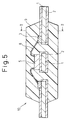
- the lead frame 101 that is illustrated is a press-molded article of copper or a copper alloy, and includes a chip-mounting portion 102, an internal lead portion 103, an external lead portion 104, and a wire-bonding portion 105. Silver layers 102a and 105a are plated on the upper surfaces of the chip-mounting portion 102 and the wire-bonding portion 105. Further, a circuit chip 106 is mounted on the chip-mounting portion 102.
- the circuit chip 106 and the wire-bonding portion 105 are connected together through a wire 107. Further, the lead frame 101, as a whole, is sealed with a sealing resin 108. In order to reinforce the adhesion between the lead frame 101 and the sealing resin 108 relying upon the anchoring effect, a black oxide film (cupric oxide CuO layer) 109 is formed on the limited portions where the silver layers 102a and 105a have not been plated. The black oxide film 109 is formed by anodizing the lead frame 101 in an organic alkali solution.
- a semiconductor package which has not been entirely covered with the sealing resin causes a new problem.
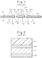
- One of the semiconductor packages of this kind is a semiconductor package called QFN (quad flat non-leaded) package.
- the leads of the lead frame and the die pads are exposed from the surface of the sealing resin. That is, as schematically illustrated in Fig. 2 partly on an enlarged scale, the lead frame includes a conductor substrate 111 of copper and Ni-plated layers 112a and 112b plated on both surfaces thereof, and only the side mounting a semiconductor element (not shown) is covered with the sealing resin 119. Therefore, the Ni-plated layer 112a positioned on the outer side of the semiconductor package is exposed to the outside.
- the semiconductor package equipped with an externally exposed heat-radiating plate too, is included in this type of semiconductor package.
- portions of the packaging component exposed to the outside are causing a new problem. That is, the exposed portions tend to be scarred or stained while the semiconductor package is being handled, deteriorating the appearance and quality of the product, making the restoration difficult and, further, impairing the laser marking operation.
- most of the scars are caused by abrasion, scratching and holding, and stains are caused by chemicals and by fingerprints (skin fat), and none of them can be neglected.
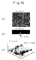
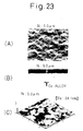
- the occurrence of scars on the packaging components is described below with reference to Figs. 3 and 4 .
- the reel-like copper lead frame was plated with a rough-surface Ni layer, cut into a sheet size for shipping, and a fixing tape was applied to secure the leads for suppressing dispersion of the leads.
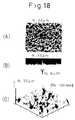
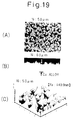
- the surface state of the Ni-plated layer of the resulting lead frame was observed through a microscope (x50) to confirm a line, considered to be a scar due to abrasion, as illustrated in Fig. 3(A) .
- the scar due to abrasion was further observed on an enlarged scale by using an electron microscope (x2,000) to confirm that the crystals had been crushed on the portion abraded by the metal mold as illustrated in Fig. 3(B) .
- the same lead frame was further observed for its surface state of the Ni-plated layer of another portion using the microscope (x50) to confirm a scar presumably due to holding as illustrated in Fig. 4(A) .
- the pattern of the scar was further observed on an enlarged scale using the electron microscope (x2,000) to confirm that the crystals had been crushed at a portion held by the metal mold as illustrated in Fig. 4(B) .
- the Ni-plated layer 112b has a smooth surface without solving the problem of insufficient adhesion between the sealing resin 119 and the Ni-plated layer 112b.
- JP 09 331009 discloses a lead frame, which is made of a copper alloy and comprises a die pad for mounting a semiconductor element and which is subjected to partial plating with a noble metal for wire bonding or die bonding. Aiming to prevent delamination due to formation of a copper oxide on the surface of the lead frame, the die pad is subjected, at least on a rear side where the semiconductor element is not mounted, to electroless copper plating at a surface roughness Ra (JIS B0601) in the range of 0.05 to 0.1 ⁇ m.
- Ra surface roughness
- JP 10 173 117 discloses a lead frame, which comprises a chip mounted therein, a resin bank formed like a frame surrounding the chip on one surface of the lead frame, a substrate formed on the other surfaces of the lead frame to surround the lead frame, and a cap bonded to the bank to form a hollow space to seal the chip.
- the surface of the lead frame is divided into first regions, which are in contact with the substrate and the bank, and second regions other than the first regions.
- a Ni plating having a high adhesion to the resin is applied to said first regions.
- An Au plating having a low adhesion to the resin but a high conductivity and bonding power is applied to said second regions.
- JP 63 160 367 discloses an iron lead frame composed of an iron/nickel alloy and having a part to be sealed formed by a film composed mainly of at least one out of metals such as copper, zinc, tin, nickel and/or its compound whose adhesion performance in relation to a sealing resin is good.
- the surface roughness of the coated film is made to be at least more than 1 ⁇ m, and in addition, its surface is treated by various chemical processes, in order to enhance the affinity between this coated film and a sealing resin.
- a lead frame comprises a metal substrate made of copper or a copper alloy or an iron-nickel alloy, a nickel thin intermediate layer and an outermost protection layer made of either palladium or a palladium alloy.
- the protection layer cannot be formed to a uniform thickness because of a nonuniform nuclear growth within the plating solution using a DC current method.
- a lead frame comprises a metal substrate made of copper or a copper alloy or an iron-nickel family alloy, a thin intermediate layer formed of nickel or nickel alloy by a plating method using a modulated current and a protection layer made of at least one metal selected from the group comprising palladium, palladium alloy, gold, gold alloy and silver alloy, formed to a thickness of 0,01 to 1,5 microinches by a plating method using a modulated current and accordingly having a relatively fine and smooth roughness.
- EP 0 579 464 corresponding to JP 06 029 439 discloses a metal insert for at least partially embedding in a molded resin mass.
- the metal insert comprises metal insert blank formed from a thin plate of Cu, Cu alloy, Ni-Fe alloy and having a pair of side frame portions and lateral frame portions, a rectangular central stage on which an integrated circuit (IC) is securely mounted by using a silver or gold paste. Then, the central stage with the IC chip is enclosed by dam-bar elements to define a closed molding cavity. A curable synthetic resin is introduced into the molding cavity so that the IC chip is sealed in the molded resin mass. - The surface of the metal insert or lead frame is subject to a surface treatment for roughening surfaces.
- the treatment comprises a first electrolytic plating process for producing a substantial quantity of copper nuclei of the size in the order of sub-microns (size of granulation at most 1.0 ⁇ m) over the surfaces of the lead frame to an average thickness of plating of less than about 1.0 ⁇ m, and a second electrolytic plating process for growing up the copper nuclei with nickel or nickel alloy to thereby produce a substantial amount of granulations over the surfaces of the lead frame such that an average thickness of plating is about 0.5 to 1.5 ⁇ m.
- a packaging component used for constituting a package mounting a semiconductor element or any other packages, having, on at least a portion of the surface thereof, a covered surface which is sealed with an insulating resin or on which an adhesive layer is applied,
- a semiconductor package comprising at least one semiconductor element in combination with a packaging component described above.
- the present invention is concerned with a packaging component used for constituting a package mounting a semiconductor element thereon, i.e., semiconductor package or any other packages.
- a packaging component used for constituting a package mounting a semiconductor element thereon, i.e., semiconductor package or any other packages.
- the semiconductor element includes a semiconductor chip such as IC chip or LSI chip.
- the semiconductor element may be mounted alone or, alternatively, as required, there may be mounted two or more semiconductor elements in any combination. Further, there may be mounted any active element or passive element instead of the semiconductor element or in combination with the semiconductor element.
- the packaging component of the present invention can be also advantageously applied to packages other than the semiconductor packages.
- Other packages suitable in the practice of the present invention include glass terminals, i.e., glass-to-metal seals.
- the packaging component is sealed by the insulating resin or has at least a covered surface to which an adhesive layer is applied.
- the packaging component of the present invention is characterized in that the adhesion is improved relative to the insulating resin or to the adhesive layer due to the presence of a rough-surface plated layer, as will be described below in detail.
- a suitable packaging component includes those widely used for the production of semiconductor packages and other packages, typically, a lead frame, a heat-radiating or -dissipating plate, etc.
- the packaging component may be used alone or in a combination of two or more components. For example, a semiconductor chip is mounted on the lead frame, and the heat-radiating plate is further attached, onto the semiconductor chip, while adhering the plate to the chip.
- the packaging component according to the invention comprises a conductor substrate and an electrically conducting layer covering the surfaces thereof.
- the electrically conducting layer may cover a whole surface of the conductor substrate or may partly cover only the required portions of the surface.
- the conductor substrate may be formed from various materials depending upon the constitution of the packaging component or the required characteristics. Suitable materials for forming the conductor substrate may include, for example, copper or an alloy or a compound thereof, as well as an alloy or compound of a metal other than copper (a non-copper metal), though the material of the conductor substrate is in no way limited thereto. Examples of the non-copper metal include aluminum, iron-nickel alloy, etc.
- the packaging component is a lead frame, for example, copper or an alloy thereof can be advantageously used as the conductor substrate, because they have excellent electric conduction and can be easily worked.
- the packaging component is a heat-radiating plate, it is desired that the conductor substrate exhibits excellent heat conduction and heat radiation. Therefore, copper, aluminum or an alloy thereof can be advantageously used as the conductor substrate.
- the electrically conducting layer may be formed from the same material as the conductor substrate or may be formed from any other materials.
- the electrically conducting layer is usually formed as a single layer. As required, however, it may be formed as a multi-layer structure having two or more layers. Desirably, the electrically conducting layer is formed as a plated layer by using a plating method. As required, however, it may be formed by a thin-film forming technology other than the plating method, such as vacuum evaporation or sputtering.
- the electrically conducting layer covering the conductor substrate must at least partly have a rough-surface plated layer having a roughened surface profile as defined in claim 1.
- the rough-surface plated layer usually has a lusterless surface.
- the portion of the packaging component is formed.
- the above portion is, typically, a portion to where the sealing resin is applied or a portion to where an adhesive layer is applied by applying an adhesive or by sticking an adhesive tape for bonding the packaging components or for the element bonding. In the present invention, these portions are particularly referred to as "covered surfaces".
- the portion where the sealing resin or the adhesive layer needs not be applied is referred to as an "uncovered surface”. That is, the portion where the packaging component of the semiconductor package or of any other package is exposed to the outer side is referred to as an "uncovered surface” so as to be distinguished from the covered surface of the packaging component.
- the rough-surface plated layer of the electrically conducting layer may be formed by a method other than the plating method, as required, but is advantageously formed by the plating method from the standpoint of ease and cost.
- an electroplating method can be advantageously used.
- preferred metals to be plated includes nickel, copper, palladium, gold, silver, tin, chromium or an alloy thereof.
- a plating bath used for forming the rough-surface plated layer may be arbitrarily modified depending upon the kind of the layer to be plated.
- the rough-surface plated layer is to be formed by using nickel
- a nickel chloride plating bath there can be advantageously used a nickel chloride plating bath.
- the nickel chloride plating bath suited in the practice of the invention may have the following composition. Nickel chloride 75 g/L Sodium thiocyanate 15 g/L Ammonium chloride 30 g/L pH 4.5 to 5.5
- the above nickel chloride plating bath can be used under, for example, the following conditions. Bath temperature normal temp. (about 25° C) Treatment time about 15 sec. to about 30 min. Cathode current density about 1 to 3 A/cm 2
- the rough-surface plated layer may be formed at different thicknesses.
- the thickness of the rough-surface plated layer varies depending upon the constitution (single layer or multiple layers) of the plated layer and the properties required for the plated layer, but is, usually, in the range of about 0.2 to 50 ⁇ m and, preferably, in the range of about 0.3 to 10 ⁇ m. In the practice of the invention, there is no particular limitation on the thickness of the rough-surface plated layer.
- the rough-surface plated layer formed as the electrically conducting layer can be formed on various portions of the packaging component as described above.
- a packaging component is preferably and typically a lead frame used for the production of a semiconductor package.
- a semiconductor package for example, one or more semiconductor elements can be mounted on a predetermined position of the lead frame, and the lead frame can substantially be entirely sealed with the insulating resin.
- the externally exposed heat-radiating plate that is partly exposed to the outer side may also be used along with the lead frame.
- the packaging component may have, on the surface thereof, both a covered surface and an uncovered surface.
- the uncovered surface is a particular surface of the surface of the packaging component that is exposed to the outer side in the absence of the insulating resin and/or the adhesive layer.
- how to use the covered surface and the uncovered surface on the surface of the packaging component can be arbitrarily varied depending upon the kind and the object of use of the packaging component. When a plurality of packaging components are used, the selection is further diversified.
- a semiconductor package is to be produced by sealing the lead frame as a packaging component with the resin, a portion of the lead frame is exposed to the outer side, and this exposed surface of the lead frame becomes the "uncovered surface” which is specifically referred to in the present invention.
- the surface of the lead frame on the side of mounting the element is in a state of being sealed with the insulating resin, and becomes the "covered surface” which is also specifically referred to in the present invention.
- the surface of the heat-radiating plate is at least partly exposed to the outer side, and this exposed portion becomes the uncovered portion.
- the bonding surface of the heat-radiating plate becomes the covered surface and the surface of the heat-radiating plate exposed to the outer side becomes the uncovered surface.
- the uncovered surface may have a rough-surface plated layer which is the same as, or similar to, the covered surface as required but, preferably, has, as the electrically conducting layer, a smooth-surface plated layer having a smooth surface profile.
- the smooth-surface plated layer is, usually, lustrous or matte, i.e., semi-lustrous.
- the smooth-surface plated layer in the uncovered surface can be formed by plating a metal which is the same as, or different from, that of the rough-surface plated layer in the covered surface.
- a preferred metal to be plated is, for example, nickel, copper, palladium, gold, silver, tin, chromium or an alloy thereof.
- the smooth-surface plated layer may be formed by a method other than the plating method as required, but is advantageously formed by the plating method from the standpoint of ease and cost.
- an electroplating method can be advantageously used.
- the plating bath used herein can be arbitrarily modified depending upon the kind of the plated layer.
- a nickel sulfamate plating bath there can be advantageously used a nickel sulfamate plating bath, a Watts nickel plating bath, a nickel bromide plating bath or a Wood's nickel plating bath.
- the nickel sulfamate plating bath suited for the practice of the invention may have the following composition. Nickel sulfamate 320 g/L Boric acid 30 g/L Nickel bromide 10 g/L pH 3.0 to 4.0
- the above nickel plating bath can be used under, for example, the following conditions.
- Bath temperature about 30 to 50° C
- Treatment time about 15 sec. to about 30 min.
- Cathode current density about 3 to 30 A/cm 2
- the smooth-surface plated layer in the uncovered surface may be formed at any desired thickness as in the formation of the rough-surface plated layer in the covered surface.
- the thickness of the smooth-surface plated layer varies depending upon the constitution (single layer or multiple layers) of the plated layer and the properties required for the plated layer, but is, usually, in the range of about 0.2 to 50 ⁇ m and, preferably, about 0.3 to 10 ⁇ m. In the practice of the invention, there is no particular limitation on the thickness of the smooth-surface plated layer.
- the rough-surface plated layer in the uncovered surface of the conductor substrate may have various roughened states as a surface profile.
- the preferred roughened state is a needle-like crystalline structure of the plating metal.
- the needle-like projections may have any shape, and typically the shape is a triangular cone, an aventurine or a feather. It is, generally, desired that the needle-like projections are distributed on the whole surface of the covered surface.
- the needle-like projections may be to simply occupy a substantial portion (e.g., about 80% or more) of the covered surface. Further, the projections need not all be of a needle shape. Depending upon the cases, some of the projections may have rounded ends without being sharpened provided the desired effect is obtained. This is because, owing to its shape, the needle-like crystalline structure of the plated metal offers an anchoring effect in addition to increasing the bonding area.
- the rough-surface plated layer disclosed herein may have a single-layer structure having the above-mentioned plated layer only or may have a multi-layer structure having two or more plated layers.
- Examples of the rough-surface plated layer having a multi-layer structure include:
- the rough-surface layer may be referred to as "surface plated layer”.
- the underlying plated layer may or may not exist, but when it exists, it may utilize the smooth-surface plated layer formed in the uncovered layer from the standpoint of decreasing the number of process steps and cost.
- the surface plated layer is to be used in combination with other layer or layers such as in claim 1, it is desired that the surface plated layer is used so as to reproduce the roughened surface profile specific to the rough-surface plated layer.
- the surface plated layer should not be formed in such a thickness that it completely covers the surface (rough surface) of the electrically conducting layer, thereby forming a flat or smooth surface.
- the surface plated layer is usually formed by plating a metal selected from the group consisting of gold, silver, copper, palladium, nickel, tin, chromium or an alloy thereof. If comparable functions and effects are obtained, however, the surface plated layer may be formed by any method other than plating. It is recommended to form a rough-surface plated layer by oxidizing the underlying plated layer.
- the surface plated layer may be formed in the form of an oxidized plated layer (oxide film) by oxidizing the underlying rough-surface plated layer.
- the oxide film is formed by thermally oxidizing, or chemically and/or electrochemically oxidizing the surface of the rough-surface plated layer.
- the surface can be roughened by oxidizing the underlying plated layer through blackening or black oxide treatment and the like.
- the blackening treatment is a conversion treatment for chemically forming an oxide film on a surface of copper or an alloy thereof.
- the invention is further concerned with a semiconductor package or any other packages equipped with the packaging component of the invention.
- the invention is particularly concerned with a semiconductor package having at least one semiconductor element in combination with the packaging component of the invention.
- the semiconductor element includes a semiconductor chip such as IC chip or LSI chip, as well as any other element.
- the packaging component is preferably a lead frame.
- a semiconductor element is mounted on a predetermined position of the lead frame and that the element mounting portion is further sealed with an insulating resin.
- the semiconductor package is the resin-sealed type semiconductor package in which the lead frame is substantially entirely sealed with the insulating resin.
- the resin-sealed type package may further has an externally exposed heat-radiating plate of which the surface is partly exposed to the outer side.
- the packaging component is a lead frame
- a package in which part of the lead frame is exposed to the outer side is a QFN (guad flat non-leaded) package.
- the semiconductor package includes a semiconductor package of which the packaging component is a heat-radiating or -dissipating plate. As in the above cases, it is also essential that the surface of the heat-radiating plate is partly exposed to the outer side from the insulating resin.
- This semiconductor package is a semiconductor package in which the semiconductor element is mounted on a wiring board, and the heat-radiating plate is bonded to the wiring board via an adhesive layer.
- the packaging component and the semiconductor package of the present invention can be advantageously carried out in a variety of embodiments.
- the invention will now be specifically described with reference to the accompanying drawings. The invention, however, is not limited to the following embodiments only.
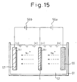
- Fig. 5 is a sectional view of a semiconductor package using a lead frame (conductor substrate) as a packaging component.
- the lead frame 1 may be substantially made of copper or an alloy thereof, or may be made of substantially a non-copper metal, and the outermost layer thereof may be made of copper or an alloy thereof.
- the non-copper alloy may be, for example, an iron-nickel (FeNi) alloy, and in such a case, the outermost layer may be formed by a plating method or by any other film-forming method by using copper or an alloy thereof.
- the lead frame is usually produced by purchasing a conductor substrate in the form of a thin plate, and machining it into the shape of a lead frame by press working or etching.
- the lead frame 1 has an electrically conducting layer (an Ni-plated layer is used herein) 2 formed on the surface thereof. As shown, the electrically conducting layer 2 is formed so as to substantially cover the outer periphery of the lead frame 1.
- the lead frame 1 has a silver-plated layer 3 for wire bonding.
- a heat spreader may be arranged in combination with the lead frame 1 to obtain higher heat-radiating performance, and in such a case, to enhance the adhesion at the time of sealing the heat spreader with an insulating resin 9, the rough-surface plated layer of the invention is advantageously applied to the surface of the heat spreader.
- a semiconductor element 5 is mounted on a predetermined position of the lead frame 1. Though not illustrated, the lead frame 1 and the semiconductor element 5 are bonded together, usually, by using a bonding medium such as an adhesive sheet, die-bonding material, etc.
- the semiconductor element 5 is, for example, an IC chip or an LSI chip. In the illustrated embodiment, only one semiconductor element 5 is mounted. However, two or more semiconductor elements may be mounted, if desired. Further, any active element or passive element may be mounted in place of the semiconductor element or in combination with the semiconductor element. That is, in this embodiment, there is no particular limitation on the kinds of the semiconductor element and others.
- the bonding wire 8 is a fine wire of, for example, gold (Au) or aluminum (Al). As required, further, the electric connection may be accomplished by using a flip chip (FC) bonding method in place of the illustrated wire bonding method.
- FC flip chip
- the whole lead frame 1 substantially constitutes the "(resin)covered surface” that is referred to in the present invention.
- the sealing resin 9 works to protect the semiconductor package 10 from the external moisture or shocks, and includes any insulating resin so far as it does not impair the functions and effects of the invention.
- suitable examples of the sealing resin include epoxy resin, polyimide resin, phenol resin and vinyl chloride resin.
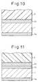
- the electrically conducting layer (Ni-plated layer) 2 of the lead frame 1 has a roughed surface profile on the side of the sealing resin 9.
- the lead frame 1 and the upper electrically conducting layer (rough-surface plated layer; Ni-plated layer) 2b has needle-like projections 12 with sharp ends in a random fashion. It is desired that the needle-like projections 12 are distributed without interruption on the surface of the rough-surface plated layer 2b.
- the needle-like projections 12 are not distributed extremely randomly. It is desired that the needle-like projections 12 formed in a triangular shape in cross section, usually, have a nearly constant height which is in a range of about 0.2 to 3 ⁇ m though it may vary depending upon the constitution of the rough-surface plated layer 2b or the plating conditions. It is further desired that the surface roughness Ra representing the height of the needle-like projections 12 is not smaller than about 50 nm.
- the electrically conducting layer (rough-surface plated layer) 2 is formed directly on the surface of the lead frame 1. As required, however, any underlying layer such as a plated layer may be interposed between the lead frame 1 and the electrically conducting layer 2.
- the rough-surface plated layer 2 formed as the electrically conducting layer in the covered surface of the lead frame 1 further has an additional layer formed thereon.
- the layer is a surface layer illustrated in Fig. 8 , which is a surface plated layer 6b. Though only one surface layer is illustrated, if formed, the surface plated layer is usually formed on both the front and back surfaces (as well as on the side surfaces) of the lead frame 1, as can be understood from Fig. 6 .
- the thickness of the surface plated layer may be varied over a wide range depending upon the desired effect but is usually in the range of about 0.005 to 1 ⁇ m and, preferably, in the range of about 0.01 to 0.05 ⁇ m.
- the surface plated layer exactly reproduces the profile of needle-like projections 12 of the underlying rough-surface plated layer 2b, and is desirably formed by a plating method suited for reproducing the projections and at a plating thickness necessary therefor.
- the surface plated layer can be advantageously formed by, for example, the plating method using gold, silver, copper, palladium, nickel, tin, chromium or an alloy thereof.
- the plating method can be carried out in accordance with the conventional methods.
- the rough-surface plated layer may be thermally, chemically and/or electrochemically oxidized to form the desired surface plated layer.
- the oxidation method for forming the surface plated layer includes a blackening or black oxide treatment method using a blackening treatment solution.
- the blackening treatment solution contains a strong alkaline compound and an oxidizing agent as its main components, and may have, for example, the following composition.
- Sodium chlorite (NaClO2) 5 to 100 g/L
- Sodium hydroxide (NaOH) 5 to 60 g/L
- Trisodium phosphate (Na3PO4) 0 to 200 g/L
- the blackening treatment solution can be used under, for example, the following treatment conditions.
- Bath temperature about 50 to 100° C Treating time about 5 sec. to 5 min.
- Current density about 0 to 10 A/dm 2
- the semiconductor package according to the present invention includes semiconductor packages other than the semiconductor package 10 described above with reference to Fig. 5 .
- the semiconductor package of the present invention may have various embodiments within the scope of the invention, and typical examples will now be described with reference to Figs. 9 , 12 and 13 .
- Fig. 9 is a sectional view illustrating an embodiment of a semiconductor package.
- the illustrated semiconductor package 10 is called a QFN (quad flat non-leaded) package, and has the external lead 1a of the lead frame 1 and the back surface of the die pad 1b exposed from the surface of the sealing resin 9. That is, the lead frame 1 possesses both the uncovered surface exposed to the outer side as well as the covered surface in contact with the sealing resin 9.
- the semiconductor element 5 mounted on the die pad 1b has the external connection terminal (not shown) connected to the silver-plated layer (not shown) of the external lead 1a through a bonding wire (Au wire) 8.
- the lead frame 1 has a constitution that is schematically illustrated in Fig. 10 .
- the lead frame 1 is a conductor substrate of copper and has a rough-surface plated layer (Ni-plated layer here) 2b, described above, at a predetermined thickness on the surface of the side of the sealing resin 9. Further, a smooth-surface plated layer (Ni-plated layer is formed herein) 7a is formed at a predetermined thickness on the surface of the lead frame 1 at a position on the outer side of the QFN package 10.
- the illustrated lead frame 1 has the smooth-surface plated layer 7b which is the same as the smooth-surface plated layer 7a on the side of the sealing resin 9, too. That is, in the case of the QFN package 10, the smooth-surface plated layers 7a and 7b are formed on both surfaces of the lead frame 1, and the rough-surface plated layer (Ni-plated layer) 2b can be selectively formed on only one surface thereof.
- Fig. 12 is a sectional view illustrating another embodiment of the semiconductor package.
- a heat-radiating aluminum plate (also called heat sink) 4 is bonded to the lead frame 1 through an adhesive tape 13, and the semiconductor element 5 is mounted on the heat-radiating plate 4.
- the heat-radiating plate 4 can be made of copper or any other highly heat conducting metallic material, in addition to aluminum.
- the semiconductor element 5 mounted on the heat-radiating plate 4 has an external connection terminal (not shown) that is connected to the silver-plated layer (not shown) of the lead frame 1 via the bonding wire (Au wire) 8.
- the present invention can be applied not only to the lead frame 1 but also to the heat-radiating plate 4. This is because the lead frame 1 has the covered surface which is in contact with the sealing resin 9 and the heat-radiating plate 4 has the uncovered surface exposed to the outer side as well as the covered surface in contact with the sealing resin 9.
- the rough-surface layer is plated in the covered surfaces of the lead frame 1 and of the heat-radiating plate 4, and the smooth-surface layer is plated in the uncovered surface of the heat-radiating plate 4.
- Fig. 13 is a sectional view illustrating another embodiment of the semiconductor package.
- the semiconductor element 5 is bonded through flip chips (FC) onto a circuit board 15 via gold (Au) bumps 17, and is sealed with the sealing resin 9. Further, solder balls 18 are mounted as external connection terminals on the circuit board 15.
- a heat-radiating plate (also called a heat slug) 14 made of copper or a copper alloy is bonded to the back surfaces of the circuit board 15 and of the semiconductor element 5.
- the heat-radiating plate 14 has a recessed portion for accommodating the semiconductor element 5.
- the heat-radiating plate 14 and the circuit board 15 are bonded together through an adhesive layer (polyimide tape) 16, and the present invention can be applied to this bonding portion.
- the bonding surfaces of the heat-radiating plate 14 and of the circuit board 15 are the covered surfaces on where a rough-surface layer is plated invention. Further, the outer surface of the heat-radiating plate 14 is the uncovered surface where a smooth-surface layer is plated.
- the electrically conducting layer of the packaging component can be advantageously formed by the plating method as described above and, more preferably, by the electroplating method.
- the conventional plating method and plating apparatus can be arbitrarily used.
- the rough-surface plated layer and the smooth-surface plated layer each consisting of nickel can be advantageously formed by using a plating treatment apparatus schematically illustrated in Fig. 14 or 15 .
- a plating treatment apparatus 50 includes a treatment vessel 51 and a treatment solution (nickel-plating bath) 52.
- the treatment solution 52 can have an optimum composition for a layer that is to be plated.
- a conductor substrate (precursor of packaging component) 1 such as a lead frame immersed in the treatment vessel 51 can be conveyed in a direction of an arrow by accessory guide rollers (not shown).
- the treatment solution 52 is maintained at normal temperatures when it is, for example, a nickel chloride-plating bath, and the residence time of the conductor substrate 1 is about 15 seconds to about 30 minutes.
- the treatment vessel 51 includes two pieces of platinum electrode plates (+) 54 and 55 connected to a rectifier 56 for electroplating. It is also allowable to use nickel chips instead of the platinum electrode plates.
- the conductor substrate 1, too, is served with power from the rectifier 56.
- the plating treatment apparatus 50 of Fig. 14 is useful for separately forming the rough-surface plated layer and the smooth-surface plated layer.
- the plating treatment apparatus 50 of Fig. 14 can be used after modification thereof.
- a method of shielding the non-plating surface with a mechanical mask or a resist film, or an electrolytic shielding method can be selectively precipitated on only the exposed surface of the conductor substrate by conducting the electrolytic plating in a state where the non-plating surface is shielded.
- Fig. 15 illustrates a modification of the plating treatment apparatus 50 of Fig. 14 for effecting the electrolytic shielding method.
- two rectifiers 56a and 56b are provided for one treatment vessel 51 to form two electric circuits in the treatment vessel 51.
- One electric circuit connected to the rectifier 56a includes a platinum electrode plate (which may be a nickel chip) 55
- another electric circuit connected to the rectifier 56b includes a dummy electrode plate 57 instead of the platinum electrode plate 54 in Fig. 14 .
- the dummy electrode plate 57 is arranged to prevent nickel being precipitated on the shielding surface of the conductor substrate 1.
- Ni + nickel ions that have passed through the back surface of the conductor substrate 1 can be selectively precipitated on the surface of the dummy electrode plate 57. This method makes it easy to form the rough-surface plated layer on only one surface of the conductor substrate 1.
- a copper alloy (trade name: CDA194) containing a trace amount of iron (Fe) was used as a starting material, and the surface on one side thereof was electroplated with nickel to form rough-surface Ni-plated layers at different thicknesses, thereby preparing the following four samples.
- Sample A layer thickness of 0.5 ⁇ m
- Sample B layer thickness of 1.0 ⁇ m
- Sample C layer thickness of 3.0 ⁇ m
- Sample D layer thickness of 5.0 ⁇ m
- the composition of the electroplating bath and the plating conditions used in this example were as follows: Nickel chloride plating bath: Nickel chloride 75 g/L Sodium thiocyanate 15 g/L Ammonium chloride 30 g/L pH: about 4.5 to 5.5 Bath temperature: normal temperature (about 25° C) Cathode current density: about 1 to 3 A/cm 2
- Nickel chloride plating bath Nickel chloride 75 g/L Sodium thiocyanate 15 g/L Ammonium chloride 30 g/L pH: about 4.5 to 5.5
- Bath temperature normal temperature (about 25° C)
- Cathode current density about 1 to 3 A/cm 2
- the samples A to D having lusterless surface each was:
- a copper alloy (trade name: CDA194) containing a trace amount of iron (Fe) was used as a starting material, and the surface on one side thereof was electroplated with nickel to form smooth-surface Ni-plated layers at different thicknesses, thereby preparing the following four samples.
- Sample I layer thickness of 0.5 ⁇ m
- Sample II layer thickness of 1.0 ⁇ m
- Sample III layer thickness of 3.0 ⁇ m
- Sample IV layer thickness of 5.0 ⁇ m
- the composition of the electroplating bath and the plating conditions used in this example were as follows: Nickel sulfamate plating bath: Nickel sulfamate 320 g/L Boric acid 30 g/L Nickel bromide 10 g/L pH: about 3.0 to 4.0 Bath temperature: about 30 to 50° C Cathode current density: about 3 to 30 A/cm 2
- Nickel sulfamate plating bath Nickel sulfamate 320 g/L Boric acid 30 g/L Nickel bromide 10 g/L pH: about 3.0 to 4.0
- Bath temperature about 30 to 50°
- Cathode current density about 3 to 30 A/cm 2
- the samples I to IV having matte surface each was:
- the reel-like copper lead frame was plated with smooth-surface Ni layer according to the method described above, cut into a sheet size for shipping, and a fixing tape was stuck to secure the leads for suppressing dispersion of the leads.
- the surface state of the Ni-plated layer of the resulting lead frame was observed through a microscope (x50). As shown in Fig. 24(A) , however, there was recognized no scar due to abrasion that was observed in Fig. 3(A) . Even the observation on an enlarged scale by using the electron microscope (x2,000) showed no change in the crystalline state of the Ni-plated layer as shown in Fig. 24(B) .
- the same lead frames were observed for their surface states of the Ni-plated layer at different positions by using the microscope (x50). As shown in Fig.
- cups 21 in the shape of a circular truncated cone having a height h of 3 mm, a bottom diameter d 1 of 3.568 mm, an upper diameter d 2 of 3 mm and a surface area of 10.2 mm 2 as illustrated in Fig. 26A were molded by using the following two types of sealing resins:
- the cup 21 was placed on a sample (lead frame) 1 as illustrated in Fig. 26(B) and was heated (post-cured) at 175° C for 6 hours.
- a gauge (not shown) was pushed onto the cup 21 and was moved in the direction of an arrow shown in Fig 26(B) to measure the shear strength.
- the shearing test was conducted at a gauge height of 50 ⁇ m, at a speed of 200 ⁇ m /sec and at a shearing temperature of room temperature (about 25° C).
- Fig. 27 is a graph plotting the cup shear strengths measured for each of the samples by using the sealing resin A
- Fig. 28 is a graph plotting the cup shear strengths measured for each of the samples by using the sealing resin B.
- the adhesion of the resin to the rough-surface Ni-plated layer and to the smooth-surface Ni-plated layer each having a three-layer structure was evaluated in terms of a cup shear strength.
- Rough-surface nickel layers having different thicknesses were electroplated on the surface on one side of the copper alloy (trade name: DCA194) according to the method described in Example 1 above. Then, as illustrated in Fig. 29(B) , a palladium (Pd) layer having a thickness of 0.05 ⁇ m and a gold (Au) layer having a thickness of 0.005 ⁇ m were successively plated on the rough-surface Ni-plated layer. The surface of the Au-plated layer was reproducing the rough surface of the underlying Ni-plated layer.
- the samples I-1 to I-7 and the samples A-1 to A7 prepared as described above were subjected to measurement of cup shear strengths by the same method as that of Example 3.
- cups in the shape of a circular truncated cone were molded by using the sealing resin B of the BNL type.
- Fig. 30 is a graph plotting the cup shear strengths measured for each of the samples.
- the samples I-1 to I-7 were aged in air on a hot plate heated at 300° C for 10 seconds to measured for their cup shear strengths according to the procedure specified under SEMI Standard G69-0996 to evaluate the adhesion of the resin to the smooth-surface Ni-plated layer.
- the aging treatment was conducted simulating a high-temperature treatment in the solder reflowing step included in the practical production of the semiconductor package.
- Fig. 31 is a graph plotting the cup shear strengths measured for each of the samples.
- Fig. 32 is a graph plotting the cup shear strengths measured for each of the samples.
- Fig. 33 is a graph plotting the cup shear strengths measured for each of the samples.
- the adhesion of the resin to the plated layer is very larger in the case of the rough-surface plated layer than that of the resin to the smooth-surface plated layer, and the adhesion does not greatly decrease due to the aging.
- a packaging component such as a lead frame or a heat-radiating plate which, when used for the production of semiconductor packages or the like, exhibits excellent adhesion of the sealing resin or the adhesive to the packaging component without permitting the adhesion to be deteriorated.
- the packaging component of the present invention exhibits excellent adhesion, does not permit the adhesion to be deteriorated, does not cause defects such as scars or stains while the semiconductor packages or the like is being produced or is handled, and contributes greatly to improving the productivity, and appearance and quality.
- packaging component of the invention makes it possible to produce various types of products inclusive of the semiconductor packages as well as the packages having excellent appearance easily with a good yield.
- an electrically conducting layer can be applied in combination with a rough-surface plated layeras defined in claim 1 to the packaging component, it becomes possible to satisfy the diversifying requirements for the semiconductor packages, such as improving the adhesion and preventing scars and stains during the handling.
Landscapes
- Chemical & Material Sciences (AREA)
- Engineering & Computer Science (AREA)
- Materials Engineering (AREA)
- Organic Chemistry (AREA)
- Metallurgy (AREA)
- Chemical Kinetics & Catalysis (AREA)
- Electrochemistry (AREA)
- Crystallography & Structural Chemistry (AREA)
- Computer Hardware Design (AREA)
- Microelectronics & Electronic Packaging (AREA)
- Power Engineering (AREA)
- Physics & Mathematics (AREA)
- Condensed Matter Physics & Semiconductors (AREA)
- General Physics & Mathematics (AREA)
- Electromagnetism (AREA)
- Food Science & Technology (AREA)
- Lead Frames For Integrated Circuits (AREA)
- Structures Or Materials For Encapsulating Or Coating Semiconductor Devices Or Solid State Devices (AREA)
- Cooling Or The Like Of Semiconductors Or Solid State Devices (AREA)
- Electroplating Methods And Accessories (AREA)
Claims (20)
- Élément de conditionnement utilisé pour constituer un boîtier (10) supportant un élément semi-conducteur (5) ou tout autre boîtier, comportant, sur au moins une partie de sa surface, une surface recouverte qui est scellée au moyen d'une résine isolante (9) ou sur laquelle est appliquée une couche adhésive (13, 16),
ledit élément de conditionnement comprenant un substrat conducteur (1) et une couche conductrice d'électricité (2) recouvrant, totalement ou en partie, sa surface,
ladite couche conductrice d'électricité (2) sur ladite surface recouverte présentant une structure multicouche de deux couches ou plus,
caractérisé en ce que la couche conductrice d'électricité (2) comprend une couche plaquée à surface rugueuse (2a, 2b) ayant une structure cristalline aciculaire d'un métal de placage et une couche plaquée de surface (6b) formées, dans cet ordre, sur le substrat conducteur (1), la couche plaquée de surface (6b) reproduisant les protubérances aciculaires (12) de la couche plaquée à surface rugueuse (2b). - Élément de conditionnement selon la revendication 1, dans lequel la totalité de la surface dudit élément de conditionnement est occupée par ladite surface recouverte.
- Élément de conditionnement selon la revendication 1, dans lequel la surface dudit élément de conditionnement comprend une surface non recouverte, exposée sur le côté extérieur en l'absence de ladite résine isolante (9) et/ou ladite couche adhésive (13, 16), en plus de ladite surface recouverte, et, dans ladite surface non recouverte, ledit film conducteur d'électricité (2) comprend une couche plaquée à surface lisse (7a), qui est une couche plaquée ayant un profil de surface lisse relativement au profil de surface de la couche plaquée à surface rugueuse.
- Élément de conditionnement selon la revendication 3, dans lequel ladite couche plaquée à surface rugueuse (2a, 2b) dans ladite surface recouverte et ladite couche plaquée à surface lisse (7a) dans ladite surface non recouverte sont formées à partir de métaux de plaquage identiques ou différents.
- Élément de conditionnement selon la revendication 3 ou 4, dans lequel ladite couche plaquée à surface rugueuse (2a, 2b) dans ladite surface recouverte et ladite couche plaquée à surface lisse (7a) dans ladite surface non recouverte ont des épaisseurs de couche identiques ou différentes.
- Élément de conditionnement selon la revendication 4 ou 5, dans lequel ledit métal de plaquage est du nickel, du cuivre, du palladium, de l'or, de l'argent, de l'étain, du chrome ou un alliage de ceux-ci.
- Élément de conditionnement selon la revendication 1, dans lequel ledit métal de plaquage est du nickel, du cuivre, du palladium ou un alliage de ceux-ci.
- Élément de conditionnement selon la revendication 1, dans lequel ladite couche conductrice d'électricité (2) comprend une couche plaquée à surface lisse (7b), une couche plaquée à surface rugueuse (2b) et une couche plaquée de surface (6b) formées, dans cet ordre, sur le substrat conducteur (1).
- Élément de conditionnement selon l'une quelconque des revendications 1 à 8, dans lequel ladite couche plaquée de surface (6b) comprend un métal sélectionné dans le groupe consistant en or, argent, cuivre, palladium, nickel, étain, chrome et un alliage de ceux-ci.
- Élément de conditionnement selon l'une quelconque des revendications 1 à 9, dans lequel ladite couche plaquée de surface (6b) est une couche ayant la surface rendue rugueuse par oxydation de la couche plaquée à surface rugueuse (2b) sous-jacente.
- Élément de conditionnement selon l'une quelconque des revendications 1 à 10, dans lequel ledit substrat conducteur (1) comprend un alliage ou un composé de cuivre ou un métal non cuivre.
- Élément de conditionnement selon la revendication 11, dans lequel ledit métal non cuivre est de l'aluminium ou du nickel-fer.
- Élément de conditionnement selon l'une quelconque des revendications 1 à 12, qui est une grille de connexion (1), une plaque de rayonnement thermique (4, 14) ou une combinaison de celles-ci.
- Boîtier de semi-conducteur comprenant au moins un élément semi-conducteur (5) en combinaison avec un élément de conditionnement décrit selon l'une quelconque des revendications 1 à 13.
- Boîtier de semi-conducteur selon la revendication 14, dans lequel ledit élément de conditionnement est une grille de connexion (1), ledit élément semi-conducteur (5) est monté en une position prédéterminée sur ladite grille de connexion (1) et est scellé au moyen d'une résine isolante (9).
- Boîtier de semi-conducteur selon la revendication 15, dans lequel la surface totale de ladite grille de connexion (1) est scellée au moyen de la résine isolante (9).
- Boîtier de semi-conducteur selon la revendication 16, comprenant, en outre, une plaque de rayonnement thermique (4, 14) exposée extérieurement dont la surface est partiellement exposée sur le côté extérieur.
- Boîtier de semi-conducteur selon la revendication 15, dans lequel ladite grille de connexion (1) est en partie exposée sur le côté extérieur.
- Boîtier de semi-conducteur selon la revendication 14, dans lequel ledit élément de conditionnement est une plaque de rayonnement thermique (4, 14) dont la surface est partiellement exposée sur le côté extérieur.
- Boîtier de semi-conducteur selon la revendication 19, dans lequel ledit élément semi-conducteur (5) est monté sur un tableau de câblage (15), et ladite plaque de rayonnement thermique (14) est liée audit tableau de câblage (15) par le biais d'une couche adhésive (16).
Applications Claiming Priority (2)
| Application Number | Priority Date | Filing Date | Title |
|---|---|---|---|
| JP2003145216 | 2003-05-22 | ||
| JP2003145216A JP3841768B2 (ja) | 2003-05-22 | 2003-05-22 | パッケージ部品及び半導体パッケージ |
Publications (3)
| Publication Number | Publication Date |
|---|---|
| EP1480270A2 EP1480270A2 (fr) | 2004-11-24 |
| EP1480270A3 EP1480270A3 (fr) | 2005-07-13 |
| EP1480270B1 true EP1480270B1 (fr) | 2016-07-20 |
Family
ID=33095467
Family Applications (1)
| Application Number | Title | Priority Date | Filing Date |
|---|---|---|---|
| EP04010184.2A Expired - Lifetime EP1480270B1 (fr) | 2003-05-22 | 2004-04-29 | Dispositif d'emballage et boîtier semi-conducteur |
Country Status (7)
| Country | Link |
|---|---|
| US (1) | US7190057B2 (fr) |
| EP (1) | EP1480270B1 (fr) |
| JP (1) | JP3841768B2 (fr) |
| KR (1) | KR101069198B1 (fr) |
| CN (1) | CN100433300C (fr) |
| MY (1) | MY141960A (fr) |
| TW (1) | TWI351078B (fr) |
Families Citing this family (94)
| Publication number | Priority date | Publication date | Assignee | Title |
|---|---|---|---|---|
| US7630492B2 (en) * | 2002-10-03 | 2009-12-08 | Daniel Lecomte | Secure audio stream scramble system |
| DE102004047522B3 (de) * | 2004-09-28 | 2006-04-06 | Infineon Technologies Ag | Halbleiterchip mit einer Metallbeschichtungsstruktur und Verfahren zur Herstellung desselben |
| JP4543943B2 (ja) * | 2005-01-26 | 2010-09-15 | パナソニック株式会社 | 半導体装置用リードフレームの製造方法 |
| US7192809B2 (en) * | 2005-02-18 | 2007-03-20 | Texas Instruments Incorporated | Low cost method to produce high volume lead frames |
| KR100819800B1 (ko) * | 2005-04-15 | 2008-04-07 | 삼성테크윈 주식회사 | 반도체 패키지용 리드 프레임 |
| JP2006303215A (ja) * | 2005-04-21 | 2006-11-02 | Denso Corp | 樹脂封止型半導体装置 |
| JP4857594B2 (ja) | 2005-04-26 | 2012-01-18 | 大日本印刷株式会社 | 回路部材、及び回路部材の製造方法 |
| KR100702968B1 (ko) * | 2005-11-24 | 2007-04-03 | 삼성전자주식회사 | 플로팅된 히트 싱크를 갖는 반도체 패키지와, 그를 이용한적층 패키지 및 그의 제조 방법 |
| US20090146280A1 (en) * | 2005-11-28 | 2009-06-11 | Dai Nippon Printing Co., Ltd. | Circuit member, manufacturing method of the circuit member, and semiconductor device including the circuit member |
| DE102006001602A1 (de) * | 2006-01-11 | 2007-05-24 | Infineon Technologies Ag | Halbleiterbauteil und Verfahren zu seiner Herstellung |
| CN100435323C (zh) * | 2006-01-23 | 2008-11-19 | 旭宏科技有限公司 | 用于晶片封装的散热片及其制造方法 |
| JP4591362B2 (ja) * | 2006-01-25 | 2010-12-01 | 株式会社デンソー | 電子装置の製造方法 |
| JP2007258205A (ja) * | 2006-03-20 | 2007-10-04 | Denso Corp | 電子装置およびその製造方法 |
| DE102006018765A1 (de) * | 2006-04-20 | 2007-10-25 | Infineon Technologies Ag | Leistungshalbleiterbauelement, Leistungshalbleiterbauteil sowie Verfahren zu deren Herstellung |
| WO2007129132A1 (fr) * | 2006-05-10 | 2007-11-15 | Infineon Technologies Ag | Ensemble semi-conducteur et méthode d'assemblage d'un ensemble semi-conducteur |
| KR101058986B1 (ko) * | 2006-06-22 | 2011-08-23 | 다이니폰 인사츠 가부시키가이샤 | 수지 밀봉형 반도체 장치와 그 제조 방법, 반도체 장치용 기재 및 적층형 수지 밀봉형 반도체 장치 |
| JP5153316B2 (ja) * | 2007-12-21 | 2013-02-27 | 新光電気工業株式会社 | 半導体パッケージ用放熱板およびそのめっき方法 |
| JP4931835B2 (ja) * | 2008-01-16 | 2012-05-16 | 株式会社デンソー | 半導体装置 |
| JP5243975B2 (ja) * | 2008-02-04 | 2013-07-24 | 新光電気工業株式会社 | 熱伝導部材を有する半導体パッケージ放熱用部品及びその製造方法 |
| TWI407542B (zh) * | 2008-06-19 | 2013-09-01 | Unimicron Technology Corp | 嵌埋半導體元件之電路板及其製法 |
| US20090315159A1 (en) * | 2008-06-20 | 2009-12-24 | Donald Charles Abbott | Leadframes having both enhanced-adhesion and smooth surfaces and methods to form the same |
| KR101241735B1 (ko) * | 2008-09-05 | 2013-03-08 | 엘지이노텍 주식회사 | 리드 프레임 및 그 제조방법 |
| JP4853508B2 (ja) * | 2008-11-05 | 2012-01-11 | 住友金属鉱山株式会社 | リードフレームの製造方法 |
| JP2010171200A (ja) * | 2009-01-22 | 2010-08-05 | Shinko Electric Ind Co Ltd | 半導体パッケージ放熱用部品 |
| KR20100103015A (ko) * | 2009-03-12 | 2010-09-27 | 엘지이노텍 주식회사 | 리드 프레임 및 그 제조방법 |
| JP2010245417A (ja) * | 2009-04-09 | 2010-10-28 | Renesas Electronics Corp | 半導体装置およびその製造方法 |
| JP2011003565A (ja) * | 2009-06-16 | 2011-01-06 | Hitachi Automotive Systems Ltd | 電子ユニット |
| KR101113891B1 (ko) * | 2009-10-01 | 2012-02-29 | 삼성테크윈 주식회사 | 리드 프레임 및 리드 프레임 제조 방법 |
| WO2012036281A1 (fr) * | 2010-09-17 | 2012-03-22 | ローム株式会社 | Dispositif d'émission de lumière à semi-conducteurs, procédé pour sa production et dispositif d'affichage |
| KR101802850B1 (ko) * | 2011-01-11 | 2017-11-29 | 해성디에스 주식회사 | 반도체 패키지 |
| JP2012174696A (ja) * | 2011-02-17 | 2012-09-10 | Fujikura Ltd | 接合面を備えた放熱装置およびその表面処理方法 |
| US8966747B2 (en) | 2011-05-11 | 2015-03-03 | Vlt, Inc. | Method of forming an electrical contact |
| JP5408457B2 (ja) * | 2011-09-02 | 2014-02-05 | 住友金属鉱山株式会社 | リードフレームの製造方法 |
| JP6089341B2 (ja) * | 2011-12-22 | 2017-03-08 | オーエム産業株式会社 | めっき品及びその製造方法 |
| JP5083472B1 (ja) * | 2012-01-25 | 2012-11-28 | パナソニック株式会社 | Ledパッケージの製造方法 |
| JP6038598B2 (ja) * | 2012-11-08 | 2016-12-07 | パナソニック デバイスSunx竜野株式会社 | Ledパッケージ、led発光素子及びそれらの製造方法 |
| WO2013111253A1 (fr) * | 2012-01-25 | 2013-08-01 | パナソニック株式会社 | Boîtier de diode électroluminescente, élément électroluminescent à diode électroluminescente, et procédé de fabrication correspondant |
| CN102543910A (zh) * | 2012-02-06 | 2012-07-04 | 三星半导体(中国)研究开发有限公司 | 芯片封装件及其制造方法 |
| CN102817056B (zh) * | 2012-08-15 | 2015-03-25 | 中山品高电子材料有限公司 | 一种引线框架钯镍合金镀层的电镀工艺 |
| CN102892279B (zh) * | 2012-09-06 | 2015-09-02 | 刘伟德 | 一种电磁屏蔽材料、应用及其制造方法 |
| JP2013048280A (ja) * | 2012-10-30 | 2013-03-07 | Renesas Electronics Corp | 半導体装置の製造方法 |
| JP5678980B2 (ja) * | 2013-03-18 | 2015-03-04 | 大日本印刷株式会社 | 回路部材の製造方法 |
| JP2014192222A (ja) * | 2013-03-26 | 2014-10-06 | Shinko Electric Ind Co Ltd | リードフレーム及び半導体装置 |
| CN105264659B (zh) | 2013-07-05 | 2018-05-18 | 瑞萨电子株式会社 | 半导体装置 |
| JP6278297B2 (ja) * | 2013-07-24 | 2018-02-14 | 株式会社日立製作所 | 接合構造およびそれを用いた半導体装置 |
| DE102013215246A1 (de) * | 2013-08-02 | 2015-02-05 | Robert Bosch Gmbh | Elektronikmodul mit Leiterplatten und anspritzbarem Kunststoff-Dichtring, insbesondere für ein Kfz-Getriebesteuergerät, und Verfahren zum Fertigen desselben |
| KR101538543B1 (ko) | 2013-08-13 | 2015-07-22 | 앰코 테크놀로지 코리아 주식회사 | 반도체 디바이스 및 그 제조 방법 |
| JP2015056540A (ja) * | 2013-09-12 | 2015-03-23 | 株式会社東芝 | 半導体装置及びその製造方法 |
| JP6366032B2 (ja) * | 2013-11-29 | 2018-08-01 | 大口マテリアル株式会社 | リードフレームおよびその製造方法 |
| CN104332563A (zh) * | 2014-09-01 | 2015-02-04 | 京东方科技集团股份有限公司 | 一种封装方法、显示面板及其制作方法、显示装置 |
| CN104113979B (zh) * | 2014-02-13 | 2017-06-30 | 美的集团股份有限公司 | 铝基线路板及其制备方法和全封装电子元件 |
| JP2014146827A (ja) * | 2014-03-27 | 2014-08-14 | Dainippon Printing Co Ltd | 回路部材の表面積層構造 |
| WO2015198724A1 (fr) | 2014-06-23 | 2015-12-30 | 富士電機株式会社 | Module semi-conducteur intégré à dispositif de refroidissement |
| JP6555927B2 (ja) * | 2015-05-18 | 2019-08-07 | 大口マテリアル株式会社 | 半導体素子搭載用リードフレーム及び半導体装置の製造方法 |
| US10264664B1 (en) | 2015-06-04 | 2019-04-16 | Vlt, Inc. | Method of electrically interconnecting circuit assemblies |
| JP6191664B2 (ja) * | 2015-08-21 | 2017-09-06 | 大日本印刷株式会社 | 半導体装置の多面付け体および半導体装置 |
| US10400347B2 (en) | 2015-09-28 | 2019-09-03 | Nippon Light Metal Company, Ltd. | Conductive member, and production method therefor |
| JP6650723B2 (ja) | 2015-10-16 | 2020-02-19 | 新光電気工業株式会社 | リードフレーム及びその製造方法、半導体装置 |
| JP6386514B2 (ja) * | 2015-11-06 | 2018-09-05 | 株式会社ワールドメタル | 接合部材と半田の接合方法 |
| JP6905031B2 (ja) * | 2016-02-17 | 2021-07-21 | 株式会社三井ハイテック | リードフレーム及び半導体パッケージ |
| JP6621681B2 (ja) * | 2016-02-17 | 2019-12-18 | 株式会社三井ハイテック | リードフレーム及びその製造方法、並びに半導体パッケージ |
| JP6605382B2 (ja) * | 2016-03-30 | 2019-11-13 | 新光電気工業株式会社 | 半導体装置及び半導体装置の製造方法 |
| JP6623108B2 (ja) * | 2016-03-31 | 2019-12-18 | 古河電気工業株式会社 | リードフレーム材料およびその製造方法 |
| US11336167B1 (en) | 2016-04-05 | 2022-05-17 | Vicor Corporation | Delivering power to semiconductor loads |
| US10785871B1 (en) | 2018-12-12 | 2020-09-22 | Vlt, Inc. | Panel molded electronic assemblies with integral terminals |
| WO2017179447A1 (fr) * | 2016-04-12 | 2017-10-19 | 古河電気工業株式会社 | Matériau de grille de connexion et son procédé de production |
| JP2016165005A (ja) * | 2016-04-19 | 2016-09-08 | 大日本印刷株式会社 | 半導体装置およびその製造方法、ならびに半導体装置用基板およびその製造方法 |
| US9679832B1 (en) * | 2016-07-20 | 2017-06-13 | Stmicroelectronics Sdn Bhd | Rough leadframe with a nanolayer of silver |
| IT201600086321A1 (it) * | 2016-08-19 | 2018-02-19 | St Microelectronics Srl | Procedimento per realizzare dispositivi a semiconduttore e dispositivo corrispondente |
| DE102016117841A1 (de) | 2016-09-21 | 2018-03-22 | HYUNDAI Motor Company 231 | Packung mit aufgerauter verkapselter Oberfläche zur Förderung einer Haftung |
| CN109891575B (zh) | 2016-10-18 | 2023-07-14 | 株式会社电装 | 电子装置及其制造方法 |
| TWI613768B (zh) * | 2017-03-20 | 2018-02-01 | 矽品精密工業股份有限公司 | 電子封裝件及其製法 |
| JP6269887B2 (ja) * | 2017-06-29 | 2018-01-31 | 大日本印刷株式会社 | 半導体装置の製造方法、およびリードフレームの製造方法 |
| JP6920585B2 (ja) * | 2017-07-10 | 2021-08-18 | パナソニックIpマネジメント株式会社 | 電子機器モジュール |
| KR102069659B1 (ko) | 2017-08-31 | 2020-01-23 | 해성디에스 주식회사 | 반도체 패키지 기판 제조방법 및 이를 이용하여 제조된 반도체 패키지 기판 |
| JP6654609B2 (ja) * | 2017-10-10 | 2020-02-26 | 本田技研工業株式会社 | 電力変換装置 |
| JP7016677B2 (ja) | 2017-11-21 | 2022-02-07 | 新光電気工業株式会社 | リードフレーム、半導体装置、リードフレームの製造方法 |
| CN110265376A (zh) | 2018-03-12 | 2019-09-20 | 意法半导体股份有限公司 | 引线框架表面精整 |
| JP7170498B2 (ja) * | 2018-10-24 | 2022-11-14 | 株式会社三井ハイテック | リードフレーム、及びリードフレームパッケージ |
| US11545418B2 (en) * | 2018-10-24 | 2023-01-03 | Texas Instruments Incorporated | Thermal capacity control for relative temperature-based thermal shutdown |
| JP7304145B2 (ja) | 2018-11-07 | 2023-07-06 | 新光電気工業株式会社 | リードフレーム、半導体装置及びリードフレームの製造方法 |
| CN111211059B (zh) * | 2018-11-22 | 2023-07-04 | 矽品精密工业股份有限公司 | 电子封装件及其制法与散热件 |
| SG10201811582WA (en) * | 2018-12-24 | 2020-07-29 | Delta Electronics Int’L Singapore Pte Ltd | Package structure and manufacturing method thereof |
| US11735512B2 (en) * | 2018-12-31 | 2023-08-22 | Stmicroelectronics International N.V. | Leadframe with a metal oxide coating and method of forming the same |
| JP7156641B2 (ja) * | 2019-02-14 | 2022-10-19 | 住友電工デバイス・イノベーション株式会社 | 半導体装置用のパッケージおよび半導体装置 |
| US11049817B2 (en) * | 2019-02-25 | 2021-06-29 | Nxp B.V. | Semiconductor device with integral EMI shield |
| JP6736717B1 (ja) * | 2019-03-25 | 2020-08-05 | 大口マテリアル株式会社 | 半導体素子搭載用基板 |
| JP6736716B1 (ja) * | 2019-03-22 | 2020-08-05 | 大口マテリアル株式会社 | リードフレーム |
| JP6741356B1 (ja) * | 2019-03-22 | 2020-08-19 | 大口マテリアル株式会社 | リードフレーム |
| JP6736719B1 (ja) * | 2019-03-28 | 2020-08-05 | 大口マテリアル株式会社 | 半導体素子搭載用部品、リードフレーム及び半導体素子搭載用基板 |
| JP2022113952A (ja) * | 2021-01-26 | 2022-08-05 | エイブリック株式会社 | 半導体装置およびその製造方法 |
| KR102623540B1 (ko) * | 2022-05-11 | 2024-01-11 | 해성디에스 주식회사 | 반도체 패키지 기판, 이를 포함하는 반도체 패키지, 및 반도체 패키지 기판의 제조방법 |
| US20240124999A1 (en) | 2022-09-26 | 2024-04-18 | Rohm And Haas Electronic Materials Llc | Nickel electroplating compositions for rough nickel |
| US20240117516A1 (en) | 2022-09-26 | 2024-04-11 | Rohm And Haas Electronic Materials Llc | Nickel electroplating compositions for rough nickel |
Family Cites Families (26)
| Publication number | Priority date | Publication date | Assignee | Title |
|---|---|---|---|---|
| JPH0629439B2 (ja) | 1983-09-21 | 1994-04-20 | 住友金属工業株式会社 | 石炭系重質油の精製方法 |
| JPS63160367A (ja) * | 1986-12-24 | 1988-07-04 | Hitachi Ltd | 樹脂封止型半導体装置 |
| US4888449A (en) * | 1988-01-04 | 1989-12-19 | Olin Corporation | Semiconductor package |
| JPH02209759A (ja) * | 1989-02-09 | 1990-08-21 | Shinko Electric Ind Co Ltd | リードフレーム |
| JPH03222465A (ja) * | 1990-01-29 | 1991-10-01 | Mitsubishi Electric Corp | リードフレームおよびその製造方法 |
| JPH03295262A (ja) * | 1990-04-13 | 1991-12-26 | Mitsubishi Electric Corp | リードフレームおよびその製造方法 |
| JPH04225553A (ja) * | 1990-12-27 | 1992-08-14 | Mitsubishi Electric Corp | 電子部品およびその製造方法 |
| JPH05129473A (ja) * | 1991-11-06 | 1993-05-25 | Sony Corp | 樹脂封止表面実装型半導体装置 |
| JPH05315511A (ja) * | 1991-12-25 | 1993-11-26 | Nikko Kinzoku Kk | リードフレーム材およびその製造方法 |
| JP3572628B2 (ja) * | 1992-06-03 | 2004-10-06 | セイコーエプソン株式会社 | 半導体装置及びその製造方法 |
| JP3228789B2 (ja) | 1992-07-11 | 2001-11-12 | 新光電気工業株式会社 | 樹脂用インサート部材の製造方法 |
| US5367196A (en) * | 1992-09-17 | 1994-11-22 | Olin Corporation | Molded plastic semiconductor package including an aluminum alloy heat spreader |
| JP3403221B2 (ja) * | 1993-07-05 | 2003-05-06 | 新光電気工業株式会社 | 配線基板付リードフレーム |
| US5701034A (en) * | 1994-05-03 | 1997-12-23 | Amkor Electronics, Inc. | Packaged semiconductor die including heat sink with locking feature |
| US5554569A (en) * | 1994-06-06 | 1996-09-10 | Motorola, Inc. | Method and apparatus for improving interfacial adhesion between a polymer and a metal |
| JPH09148509A (ja) | 1995-11-22 | 1997-06-06 | Goto Seisakusho:Kk | 半導体装置用リードフレーム及びその表面処理方法 |
| JPH09148508A (ja) * | 1995-11-29 | 1997-06-06 | Nippon Denkai Kk | 半導体装置用リードフレーム及びこれを用いた樹脂封止型半導体装置 |
| JPH09331009A (ja) | 1996-06-10 | 1997-12-22 | Dainippon Printing Co Ltd | リードフレームとリードフレーム部材、およびこれらを用いた樹脂封止型半導体装置 |
| JP2933038B2 (ja) * | 1996-12-09 | 1999-08-09 | 日本電気株式会社 | 中空パッケージおよびその製造方法 |
| JPH10313081A (ja) * | 1997-05-12 | 1998-11-24 | Mitsui High Tec Inc | 半導体装置およびその製造方法 |
| KR100275381B1 (ko) * | 1998-04-18 | 2000-12-15 | 이중구 | 반도체 패키지용 리드프레임 및 리드프레임도금방법 |
| JP2000031366A (ja) * | 1998-07-14 | 2000-01-28 | Dainippon Printing Co Ltd | 樹脂封止型半導体装置とそれに用いられる回路部材およびそれらの製造方法 |
| JP2000068303A (ja) * | 1998-08-24 | 2000-03-03 | Sony Corp | 半導体装置の製造方法 |
| JP2001127229A (ja) * | 1999-11-01 | 2001-05-11 | Nec Corp | リードフレーム及びそのリードフレームを用いた樹脂封止型半導体装置 |
| JP2002299538A (ja) * | 2001-03-30 | 2002-10-11 | Dainippon Printing Co Ltd | リードフレーム及びそれを用いた半導体パッケージ |
| US7049683B1 (en) * | 2003-07-19 | 2006-05-23 | Ns Electronics Bangkok (1993) Ltd. | Semiconductor package including organo-metallic coating formed on surface of leadframe roughened using chemical etchant to prevent separation between leadframe and molding compound |
-
2003
- 2003-05-22 JP JP2003145216A patent/JP3841768B2/ja not_active Expired - Lifetime
-
2004
- 2004-04-29 EP EP04010184.2A patent/EP1480270B1/fr not_active Expired - Lifetime
- 2004-04-30 US US10/835,007 patent/US7190057B2/en not_active Expired - Lifetime
- 2004-04-30 TW TW093112236A patent/TWI351078B/zh not_active IP Right Cessation
- 2004-05-07 MY MYPI20041695A patent/MY141960A/en unknown
- 2004-05-20 CN CNB2004100423680A patent/CN100433300C/zh not_active Expired - Lifetime
- 2004-05-20 KR KR1020040036130A patent/KR101069198B1/ko active IP Right Grant
Also Published As
| Publication number | Publication date |
|---|---|
| US20040232534A1 (en) | 2004-11-25 |
| CN1574300A (zh) | 2005-02-02 |
| EP1480270A3 (fr) | 2005-07-13 |
| EP1480270A2 (fr) | 2004-11-24 |
| JP2004349497A (ja) | 2004-12-09 |
| CN100433300C (zh) | 2008-11-12 |
| TWI351078B (en) | 2011-10-21 |
| JP3841768B2 (ja) | 2006-11-01 |
| TW200503192A (en) | 2005-01-16 |
| KR20040101038A (ko) | 2004-12-02 |
| MY141960A (en) | 2010-07-30 |
| KR101069198B1 (ko) | 2011-09-30 |
| US7190057B2 (en) | 2007-03-13 |
Similar Documents
| Publication | Publication Date | Title |
|---|---|---|
| EP1480270B1 (fr) | Dispositif d'emballage et boîtier semi-conducteur | |
| US7524702B2 (en) | Conductor substrate, semiconductor device and production method thereof | |
| EP0977251B1 (fr) | Dispositif a semiconducteur scelle par resine et procede de fabrication | |
| JP4698708B2 (ja) | パッケージ部品及び半導体パッケージ | |
| JP2009526381A (ja) | 半導体qfn/sonデバイス用のアルミニウム・リードフレーム | |
| JP2001110971A (ja) | 半導体パッケージ用リードフレーム及びその製造方法 | |
| JP5264939B2 (ja) | パッケージ部品及び半導体パッケージ | |
| JP2011077519A (ja) | リードフレーム及びその製造方法 | |
| CN110265377B (zh) | 引线框架表面精整 | |
| US6995042B2 (en) | Method for fabricating preplated nickel/palladium and tin leadframes | |
| US7125750B2 (en) | Leadframe with enhanced encapsulation adhesion | |
| US4767049A (en) | Special surfaces for wire bonding | |
| JP4628263B2 (ja) | パッケージ部品及びその製造方法ならびに半導体パッケージ | |
| JP3758610B2 (ja) | 電子部品実装用フィルムキャリアテープ | |
| JP2000068303A (ja) | 半導体装置の製造方法 | |
| KR101663695B1 (ko) | 리드프레임, 이를 이용한 반도체 패키지 및 그 제조방법 | |
| KR100544274B1 (ko) | 스터드 범프용 기판의 금속 적층구조 | |
| JPH09331009A (ja) | リードフレームとリードフレーム部材、およびこれらを用いた樹脂封止型半導体装置 | |
| KR100209264B1 (ko) | 반도체 리드 프레임 | |
| JP2004282103A (ja) | リードフレームの部分貴金属めっき方法 | |
| JPH09181469A (ja) | 電子部品搭載用基板の製造方法 |
Legal Events
| Date | Code | Title | Description |
|---|---|---|---|
| PUAI | Public reference made under article 153(3) epc to a published international application that has entered the european phase |
Free format text: ORIGINAL CODE: 0009012 |
|
| AK | Designated contracting states |
Kind code of ref document: A2 Designated state(s): AT BE BG CH CY CZ DE DK EE ES FI FR GB GR HU IE IT LI LU MC NL PL PT RO SE SI SK TR |
|
| AX | Request for extension of the european patent |
Extension state: AL HR LT LV MK |
|
| PUAL | Search report despatched |
Free format text: ORIGINAL CODE: 0009013 |
|
| AK | Designated contracting states |
Kind code of ref document: A3 Designated state(s): AT BE BG CH CY CZ DE DK EE ES FI FR GB GR HU IE IT LI LU MC NL PL PT RO SE SI SK TR |
|
| AX | Request for extension of the european patent |
Extension state: AL HR LT LV MK |
|
| 17P | Request for examination filed |
Effective date: 20050919 |
|
| AKX | Designation fees paid |
Designated state(s): DE FR IT NL |
|
| 17Q | First examination report despatched |
Effective date: 20090519 |
|
| GRAP | Despatch of communication of intention to grant a patent |
Free format text: ORIGINAL CODE: EPIDOSNIGR1 |
|
| INTG | Intention to grant announced |
Effective date: 20160211 |
|
| GRAS | Grant fee paid |
Free format text: ORIGINAL CODE: EPIDOSNIGR3 |
|
| GRAA | (expected) grant |
Free format text: ORIGINAL CODE: 0009210 |
|
| AK | Designated contracting states |
Kind code of ref document: B1 Designated state(s): DE FR IT NL |
|
| REG | Reference to a national code |
Ref country code: NL Ref legal event code: FP |
|
| REG | Reference to a national code |
Ref country code: DE Ref legal event code: R096 Ref document number: 602004049603 Country of ref document: DE |
|
| REG | Reference to a national code |
Ref country code: FR Ref legal event code: PLFP Year of fee payment: 14 |
|
| REG | Reference to a national code |
Ref country code: DE Ref legal event code: R097 Ref document number: 602004049603 Country of ref document: DE |
|
| PLBE | No opposition filed within time limit |
Free format text: ORIGINAL CODE: 0009261 |
|
| STAA | Information on the status of an ep patent application or granted ep patent |
Free format text: STATUS: NO OPPOSITION FILED WITHIN TIME LIMIT |
|
| 26N | No opposition filed |
Effective date: 20170421 |
|
| REG | Reference to a national code |
Ref country code: FR Ref legal event code: PLFP Year of fee payment: 15 |
|
| PGFP | Annual fee paid to national office [announced via postgrant information from national office to epo] |
Ref country code: FR Payment date: 20230309 Year of fee payment: 20 |
|
| PGFP | Annual fee paid to national office [announced via postgrant information from national office to epo] |
Ref country code: IT Payment date: 20230310 Year of fee payment: 20 |
|
| PGFP | Annual fee paid to national office [announced via postgrant information from national office to epo] |
Ref country code: NL Payment date: 20230314 Year of fee payment: 20 |
|
| PGFP | Annual fee paid to national office [announced via postgrant information from national office to epo] |
Ref country code: DE Payment date: 20230307 Year of fee payment: 20 |
|
| REG | Reference to a national code |
Ref country code: DE Ref legal event code: R071 Ref document number: 602004049603 Country of ref document: DE |
|
| REG | Reference to a national code |
Ref country code: NL Ref legal event code: MK Effective date: 20240428 |